JP6665183B2 - Plasma processing apparatus and plasma processing method - Google Patents
Plasma processing apparatus and plasma processing method Download PDFInfo
- Publication number
- JP6665183B2 JP6665183B2 JP2017529893A JP2017529893A JP6665183B2 JP 6665183 B2 JP6665183 B2 JP 6665183B2 JP 2017529893 A JP2017529893 A JP 2017529893A JP 2017529893 A JP2017529893 A JP 2017529893A JP 6665183 B2 JP6665183 B2 JP 6665183B2
- Authority
- JP
- Japan
- Prior art keywords
- group
- carrier
- frequency
- spectrum
- plasma
- Prior art date
- Legal status (The legal status is an assumption and is not a legal conclusion. Google has not performed a legal analysis and makes no representation as to the accuracy of the status listed.)
- Active
Links
- 238000012545 processing Methods 0.000 title claims description 133
- 238000003672 processing method Methods 0.000 title claims description 10
- 238000001228 spectrum Methods 0.000 claims description 95
- 238000010521 absorption reaction Methods 0.000 claims description 54
- 239000000969 carrier Substances 0.000 claims description 23
- 230000002159 abnormal effect Effects 0.000 claims description 18
- 238000001514 detection method Methods 0.000 claims description 4
- 238000010586 diagram Methods 0.000 description 25
- 238000000034 method Methods 0.000 description 20
- 239000004020 conductor Substances 0.000 description 9
- 238000001816 cooling Methods 0.000 description 6
- 238000012423 maintenance Methods 0.000 description 6
- 239000003507 refrigerant Substances 0.000 description 5
- 230000000694 effects Effects 0.000 description 4
- 230000005284 excitation Effects 0.000 description 4
- 230000008878 coupling Effects 0.000 description 3
- 238000010168 coupling process Methods 0.000 description 3
- 238000005859 coupling reaction Methods 0.000 description 3
- 238000005516 engineering process Methods 0.000 description 3
- 239000000284 extract Substances 0.000 description 3
- 230000005540 biological transmission Effects 0.000 description 2
- 238000006243 chemical reaction Methods 0.000 description 2
- VYPSYNLAJGMNEJ-UHFFFAOYSA-N silicon dioxide Inorganic materials O=[Si]=O VYPSYNLAJGMNEJ-UHFFFAOYSA-N 0.000 description 2
- 230000002123 temporal effect Effects 0.000 description 2
- 230000000903 blocking effect Effects 0.000 description 1
- 239000003990 capacitor Substances 0.000 description 1
- 239000002826 coolant Substances 0.000 description 1
- 239000000498 cooling water Substances 0.000 description 1
- 238000002474 experimental method Methods 0.000 description 1
- 239000011810 insulating material Substances 0.000 description 1
- 150000002500 ions Chemical class 0.000 description 1
- 238000005259 measurement Methods 0.000 description 1
- 239000002184 metal Substances 0.000 description 1
- 238000012986 modification Methods 0.000 description 1
- 230000004048 modification Effects 0.000 description 1
- 230000000644 propagated effect Effects 0.000 description 1
- 239000010453 quartz Substances 0.000 description 1
- 239000004065 semiconductor Substances 0.000 description 1
- 230000001360 synchronised effect Effects 0.000 description 1
- 238000012546 transfer Methods 0.000 description 1
Images


Classifications
-
- H—ELECTRICITY
- H01—ELECTRIC ELEMENTS
- H01J—ELECTRIC DISCHARGE TUBES OR DISCHARGE LAMPS
- H01J37/00—Discharge tubes with provision for introducing objects or material to be exposed to the discharge, e.g. for the purpose of examination or processing thereof
- H01J37/32—Gas-filled discharge tubes
- H01J37/32917—Plasma diagnostics
- H01J37/3299—Feedback systems
-
- H—ELECTRICITY
- H01—ELECTRIC ELEMENTS
- H01J—ELECTRIC DISCHARGE TUBES OR DISCHARGE LAMPS
- H01J37/00—Discharge tubes with provision for introducing objects or material to be exposed to the discharge, e.g. for the purpose of examination or processing thereof
- H01J37/32—Gas-filled discharge tubes
- H01J37/32009—Arrangements for generation of plasma specially adapted for examination or treatment of objects, e.g. plasma sources
- H01J37/32192—Microwave generated discharge
- H01J37/32266—Means for controlling power transmitted to the plasma
- H01J37/32275—Microwave reflectors
-
- H—ELECTRICITY
- H01—ELECTRIC ELEMENTS
- H01J—ELECTRIC DISCHARGE TUBES OR DISCHARGE LAMPS
- H01J37/00—Discharge tubes with provision for introducing objects or material to be exposed to the discharge, e.g. for the purpose of examination or processing thereof
- H01J37/32—Gas-filled discharge tubes
- H01J37/32009—Arrangements for generation of plasma specially adapted for examination or treatment of objects, e.g. plasma sources
- H01J37/32192—Microwave generated discharge
- H01J37/32266—Means for controlling power transmitted to the plasma
- H01J37/32284—Means for controlling or selecting resonance mode
-
- H—ELECTRICITY
- H01—ELECTRIC ELEMENTS
- H01J—ELECTRIC DISCHARGE TUBES OR DISCHARGE LAMPS
- H01J37/00—Discharge tubes with provision for introducing objects or material to be exposed to the discharge, e.g. for the purpose of examination or processing thereof
- H01J37/32—Gas-filled discharge tubes
- H01J37/32009—Arrangements for generation of plasma specially adapted for examination or treatment of objects, e.g. plasma sources
- H01J37/32192—Microwave generated discharge
- H01J37/32302—Plural frequencies
-
- H—ELECTRICITY
- H01—ELECTRIC ELEMENTS
- H01J—ELECTRIC DISCHARGE TUBES OR DISCHARGE LAMPS
- H01J37/00—Discharge tubes with provision for introducing objects or material to be exposed to the discharge, e.g. for the purpose of examination or processing thereof
- H01J37/32—Gas-filled discharge tubes
- H01J37/32009—Arrangements for generation of plasma specially adapted for examination or treatment of objects, e.g. plasma sources
- H01J37/32192—Microwave generated discharge
- H01J37/32311—Circuits specially adapted for controlling the microwave discharge
-
- H—ELECTRICITY
- H01—ELECTRIC ELEMENTS
- H01J—ELECTRIC DISCHARGE TUBES OR DISCHARGE LAMPS
- H01J2237/00—Discharge tubes exposing object to beam, e.g. for analysis treatment, etching, imaging
- H01J2237/245—Detection characterised by the variable being measured
- H01J2237/24564—Measurements of electric or magnetic variables, e.g. voltage, current, frequency
Description
本発明の種々の側面及び実施形態は、プラズマ処理装置及びプラズマ処理方法に関するものである。 Various aspects and embodiments of the present invention relate to a plasma processing apparatus and a plasma processing method.
マイクロ波によるプロセスガスの励起を利用したプラズマ処理装置がある。このプラズマ処理装置は、例えば、マイクロ波発振器によって単一の周波数を有するマイクロ波を生成し、マイクロ波を処理容器内に放射し、処理容器内のプロセスガスを電離してプラズマを生成する。 There is a plasma processing apparatus that utilizes the excitation of a process gas by microwaves. In this plasma processing apparatus, for example, a microwave having a single frequency is generated by a microwave oscillator, the microwave is radiated into a processing container, and a process gas in the processing container is ionized to generate plasma.
ところで、マイクロ波によるプロセスガスの励起を利用したプラズマ処理装置では、使用条件によって、マイクロ波の反射波が発生し、この反射波に起因してマイクロ波からプラズマへ吸収されるパワーが減少する場合がある。 By the way, in a plasma processing apparatus utilizing the excitation of a process gas by a microwave, a reflected wave of the microwave is generated depending on use conditions, and the power absorbed from the microwave to the plasma is reduced due to the reflected wave. There is.
これに対して、例えば、マイクロ波発振器と処理容器との間にインピーダンス整合用のチューナを設け、マイクロ波の反射波のパワーを検出し、マイクロ波の反射波のパワーが最小となるように、チューナ内の可動板の位置を調整する技術が知られている。 On the other hand, for example, a tuner for impedance matching is provided between the microwave oscillator and the processing container, the power of the reflected wave of the microwave is detected, and the power of the reflected wave of the microwave is minimized. A technique for adjusting the position of a movable plate in a tuner is known.
しかしながら、上述した従来技術では、単一の周波数を有するマイクロ波に代えて、互いに異なる周波数をそれぞれ有する複数の搬送波から成る搬送波群を用いてプラズマを生成する場合に、搬送波群のパワーをプラズマへ高効率に吸収させることが困難である。 However, in the above-described conventional technology, when plasma is generated using a carrier group consisting of a plurality of carriers each having a different frequency, instead of the microwave having a single frequency, the power of the carrier group is supplied to the plasma. It is difficult to absorb with high efficiency.
開示するプラズマ処理装置は、1つの実施態様において、処理容器と、所定の中心周波数を中心とする所定の周波数帯域に属する周波数であって、互いに異なる周波数をそれぞれ有する複数の搬送波から成る搬送波群を生成する搬送波群生成部と、前記搬送波群を用いて、前記処理容器内にプラズマを生成するプラズマ生成部と、前記搬送波群の進行波の周波数スペクトルである進行波スペクトルと、前記搬送波群の反射波の周波数スペクトルである反射波スペクトルとを検出するスペクトル検出部と、前記進行波スペクトル及び前記反射波スペクトルを用いて、前記プラズマに吸収される前記搬送波群のパワーである吸収パワーを算出し、前記吸収パワーが閾値以上となるように、前記反射波スペクトルの極小値及び当該極小値に対応する周波数を変動させるパラメータを調整する制御部とを有する。 In one embodiment, a plasma processing apparatus to be disclosed includes, in one embodiment, a processing container and a carrier group including a plurality of carriers each having a frequency different from each other and belonging to a predetermined frequency band centered on a predetermined center frequency. A carrier group generating unit that generates, a plasma generating unit that generates plasma in the processing chamber using the carrier group, a traveling wave spectrum that is a frequency spectrum of a traveling wave of the carrier group, and a reflection of the carrier group. A spectrum detection unit that detects a reflected wave spectrum that is a frequency spectrum of a wave, and calculates the absorption power that is the power of the carrier wave group absorbed by the plasma using the traveling wave spectrum and the reflected wave spectrum, The minimum value of the reflected wave spectrum and the minimum value correspond to the minimum value so that the absorption power is equal to or greater than a threshold value. And a control unit for adjusting the parameters for varying the wavenumber.
開示するプラズマ処理装置の1つの態様によれば、搬送波群のパワーをプラズマへ高効率に吸収させることができるという効果を奏する。 According to one aspect of the disclosed plasma processing apparatus, there is an effect that the power of the carrier wave group can be efficiently absorbed by the plasma.
以下、図面を参照して本願の開示するプラズマ処理装置の実施形態について詳細に説明する。なお、各図面において同一又は相当の部分に対しては同一の符号を付すこととする。 Hereinafter, embodiments of the plasma processing apparatus disclosed in the present application will be described in detail with reference to the drawings. In the drawings, the same or corresponding parts are denoted by the same reference numerals.
(第1の実施形態)
図1は、第1の実施形態に係るプラズマ処理装置の概略を示す図である。図1に示すプラズマ処理装置1は、処理容器12、ステージ14、搬送波群生成部16、アンテナ18、誘電体窓20及び制御部100を備えている。(First embodiment)
FIG. 1 is a view schematically showing a plasma processing apparatus according to the first embodiment. The
処理容器12は、プラズマ処理を行うための処理空間Sを画成している。処理容器12は、側壁12a、及び、底部12bを有する。側壁12aは、略筒形状に形成されている。以下、側壁12aの筒形状の中心において筒形状の延在する軸線Xを仮想的に設定し、軸線Xの延在方向を軸線X方向という。底部12bは、側壁12aの下端側に設けられ、側壁12aの底側開口を覆う。底部12bには、排気用の排気孔12hが設けられている。側壁12aの上端部は開口している。
The
側壁12aの上端部開口は、誘電体窓20によって閉じられている。誘電体窓20と側壁12aの上端部との間にはOリング19が介在している。誘電体窓20は、Oリング19を介して側壁12aの上端部に設けられる。Oリング19により、処理容器12の密閉がより確実なものとなる。ステージ14は、処理空間S内に収容され、被処理体Wが載置される。誘電体窓20は、処理空間Sに対向する対向面20aを有する。
The upper end opening of the
搬送波群生成部16は、所定の中心周波数を中心とする所定の周波数帯域に属する周波数であって、互いに異なる周波数をそれぞれ有する複数の搬送波から成る搬送波群を生成する。例えば、搬送波群生成部16は、基準周波数と位相を同期させたマイクロ波を発振することが可能なPLL(Phase Locked Loop)発振器と、PLL発振器に接続されたIQディジタル変調器とを有する。そして、搬送波群生成部16は、PLL発振器から発振されるマイクロ波の周波数を中心周波数に設定する。そして、搬送波群生成部16は、中心周波数であるマイクロ波の周波数を中心とする所定の周波数帯域に属する周波数であって、互いに異なる周波数をそれぞれ有する複数の搬送波をIQディジタル変調器を用いて生成することによって、搬送波群を生成する。例えば、N個の複素データシンボルを逆離散フーリエ変換し、連続信号にすれば、本発明の搬送波群を生成することが可能である。この信号の生成方法は、ディジタルテレビ放送等で用いられるOFDMA(Orthogonal Frequency-Division Multiple Access)変調方式と同様の方法で、生成可能である(例えば特許5320260号参照)。なお、搬送波群生成部16によって生成される搬送波群における中心周波数及び周波数帯域は、後述する制御部100によって制御される。
The carrier
図2は、搬送波群の生成方法の一例を説明するための図である。波形データは、予めディジタル化された符号の列で表されている。この波形データを量子化し、かつ、逆フーリエ変換することで、IデータとQデータとが分離される。そして、Iデータ及びQデータの各々が、D/A(Digital/Analog)変換され、低周波成分のみを通過させるLPF(ローパスフィルター)へ入力される。一方、PLL発振器から発振される中心周波数(fo)の搬送波(例えば、マイクロ波)から、互いに90°位相が異なる搬送波が生成される。そして、LPFから出力されるIデータ及びQデータを用いて、互いに90°位相が異なる搬送波を変調することによって、搬送波群が生成される。本実施形態における搬送波群は、中心周波数2450MHzのマイクロ波を用いて、10kHzピッチで40MHz帯域幅に搬送波を多重化したものである。隣り合う搬送波の位相を直交の関係(90°位相の異なる状態)にすることで、最も近接した、多くの搬送波を配列することができる。 FIG. 2 is a diagram illustrating an example of a method of generating a carrier wave group. The waveform data is represented by a string of codes digitized in advance. By quantizing this waveform data and performing an inverse Fourier transform, the I data and the Q data are separated. Then, each of the I data and the Q data is subjected to D / A (Digital / Analog) conversion and input to an LPF (low-pass filter) that passes only low-frequency components. On the other hand, carrier waves having a 90 ° phase difference from each other are generated from carrier waves (for example, microwaves) having a center frequency (fo) oscillated from the PLL oscillator. Then, the I and Q data output from the LPF are used to modulate the carriers that are 90 degrees out of phase from each other, thereby generating a carrier group. The carrier group in the present embodiment is obtained by multiplexing carrier waves in a 40 MHz bandwidth at a pitch of 10 kHz using a microwave having a center frequency of 2450 MHz. By setting the phases of adjacent carriers to be in an orthogonal relationship (a state in which the phases are different by 90 °), it is possible to arrange a number of carriers closest to each other.
ここで、搬送波群生成部16によって生成される搬送波群の波形を説明する。図3A〜3Dは、搬送波群の波形の一例を示す図である。図3Aは、時間軸、周波数軸及び振幅軸により構成される3次元座標空間における搬送波群の波形を示している。図3Bは、周波数軸及び振幅軸により構成される2次元座標空間における搬送波群の波形を示している。図3Cは、時間軸及び周波数軸により構成される2次元座標空間における搬送波群の波形を示している。図3Dは、時間軸及び振幅軸により構成される2次元座標空間における搬送波群の波形を示している。
Here, the waveform of the carrier wave group generated by the carrier wave
図3A〜図3Dに示すように、搬送波群は、所定の中心周波数(例えば、2.45GHz)を中心とする所定の周波数帯域(例えば、40MHz)に属する周波数であって、互いに異なる周波数をそれぞれ有する複数の搬送波(搬送波f1〜f12)から成る。各搬送波の周波数は、時間の経過に関わらず一定である。また、複数の搬送波の振幅は、同一である。各搬送波の振幅は、時間の経過に関わらず一定である。また、複数の搬送波のうち、所定の周波数帯域において周波数が隣り合う少なくとも2つの搬送波は、90°位相が異なる。例えば、周波数が隣り合う搬送波f1及び搬送波f2は、90°位相が異なる。また、所定の周波数帯域において、複数の搬送波の周波数は、一定の間隔(例えば、10kHz)を空けて配列される。 As shown in FIGS. 3A to 3D, the carrier wave group is a frequency belonging to a predetermined frequency band (for example, 40 MHz) centered on a predetermined center frequency (for example, 2.45 GHz), and different frequencies from each other. And a plurality of carrier waves (carrier waves f1 to f12). The frequency of each carrier is constant over time. Further, the amplitudes of the plurality of carriers are the same. The amplitude of each carrier is constant over time. In addition, among a plurality of carriers, at least two carriers whose frequencies are adjacent in a predetermined frequency band have a phase difference of 90 °. For example, the carrier f1 and the carrier f2 whose frequencies are adjacent have a phase difference of 90 °. Further, in a predetermined frequency band, the frequencies of a plurality of carrier waves are arranged at a constant interval (for example, 10 kHz).
図1の説明に戻る。プラズマ処理装置1は、増幅器21、導波管22、ダミーロード23、進行波スペクトル検出器24、反射波スペクトル検出器25、チューナ26、モード変換器27、及び同軸導波管28を更に備えている。
Returning to the description of FIG. The
搬送波群生成部16は、増幅器21を介して導波管22に接続されている。増幅器21は、搬送波群生成部16によって生成される搬送波群を増幅し、増幅した搬送波群を導波管22へ出力する。導波管22は、例えば、矩形導波管である。導波管22は、モード変換器27に接続されており、モード変換器27は、同軸導波管28の上端に接続されている。
The
ダミーロード23は、サーキュレーター23aを介して導波管22に接続されている。サーキュレーター23aは、処理容器12側から反射される搬送波群の反射波を抽出し、抽出した搬送波群の反射波をダミーロード23へ出力する。ダミーロード23は、サーキュレーター23aから入力される搬送波群の反射波を負荷等により熱に変換する。
The
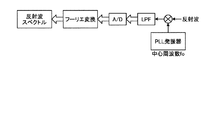
進行波スペクトル検出器24は、方向性結合器24aを介して導波管22に接続されている。方向性結合器24aは、処理容器12側へ向かう搬送波群の進行波を抽出し、抽出した搬送波群の進行波を進行波スペクトル検出器24へ出力する。方向性結合器24aの結合度は、例えば60dBmであり、方向性結合器24aの方向性は、例えば35dBmである。進行波スペクトル検出器24は、方向性結合器24aから入力される搬送波群の進行波の周波数スペクトル(以下「進行波スペクトル」と呼ぶ)を検出し、検出した進行波スペクトルを制御部100へ出力する。なお、進行波スペクトルは、搬送波群の進行波の周波数に対する、搬送波群の進行波のパワーの分布であり、例えば、搬送波群の進行波に対してフーリエ変換が施されることによって検出される。
The traveling
図4は、進行波スペクトルの検出方法の一例を説明するための図である。図4に示す例において、搬送波群生成部16によって生成された搬送波群の中心周波数がfoであり、該搬送波群の帯域幅が40MHzであるものとする。図4に示すように、方向性結合器24aから進行波スペクトル検出器24へ入力される搬送波群の進行波(以下適宜「進行波」と呼ぶ)と、PLL発振器から発振される中心周波数foの正弦波信号とが乗算されることによって、進行波が復調されて復調信号が得られる。この場合、復調信号の帯域幅は40MHzとなる。得られた復調信号は、透過帯域が約100MHzであるLPFを透過し、A/D(Analog/Digital)変換器においてA/D変換される。なお、A/D変換器のクロック周波数は、例えば、搬送波群の帯域幅の2倍以上である。ここでは、A/D変換器のクロック周波数は、80MHzであるものとする。そして、A/D変換された復調信号に対してフーリエ変換が施され、進行波に含まれる複数の周波数成分が抽出される。これらの複数の周波数成分を用いて、搬送波群の進行波の周波数に対する、搬送波群の進行波のパワーの分布、すなわち、進行波スペクトルが検出される。
FIG. 4 is a diagram for explaining an example of a method for detecting a traveling wave spectrum. In the example shown in FIG. 4, it is assumed that the center frequency of the carrier group generated by the
反射波スペクトル検出器25は、方向性結合器25aを介して導波管22に接続されている。方向性結合器25aは、処理容器12側から反射される搬送波群の反射波を抽出し、抽出した搬送波群の反射波を反射波スペクトル検出器25へ出力する。方向性結合器25aの結合度は、例えば60dBmであり、方向性結合器25aの方向性は、例えば35dBmである。反射波スペクトル検出器25は、方向性結合器25aから入力される搬送波群の反射波の周波数スペクトル(以下「反射波スペクトル」と呼ぶ)を検出し、検出した反射波スペクトルを制御部100へ出力する。なお、反射波スペクトルは、搬送波群の反射波の周波数に対する、搬送波群の反射波のパワーの分布であり、例えば、搬送波群の反射波に対してフーリエ変換が施されることによって検出される。進行波スペクトル検出器24及び反射波スペクトル検出器25は、スペクトル検出部の一例である。
The reflected
図5は、反射波スペクトルの検出方法の一例を説明するための図である。図5に示す例において、搬送波群生成部16によって生成された搬送波群の中心周波数がfoであり、該搬送波群の帯域幅が40MHzであるものとする。図5に示すように、方向性結合器25aから反射波スペクトル検出器25へ入力される搬送波群の反射波(以下適宜「反射波」と呼ぶ)と、PLL発振器から発振される中心周波数foの正弦波信号とが乗算されることによって、反射波が復調されて復調信号が得られる。この場合、復調信号の帯域幅は40MHzとなる。得られた復調信号は、透過帯域が約100MHzであるLPFを透過し、A/D変換器においてA/D変換される。なお、A/D変換器のクロック周波数は、例えば、搬送波群の帯域幅の2倍以上である。ここでは、A/D変換器のクロック周波数は、80MHzであるものとする。そして、A/D変換された復調信号に対してフーリエ変換が施され、反射波に含まれる複数の周波数成分が抽出される。これらの複数の周波数成分を用いて、搬送波群の反射波の周波数に対する、搬送波群の反射波のパワーの分布、すなわち、反射波スペクトルが検出される。
FIG. 5 is a diagram for explaining an example of a method of detecting a reflected wave spectrum. In the example shown in FIG. 5, it is assumed that the center frequency of the carrier group generated by the
チューナ26は、導波管22に設けられ、搬送波群生成部16と、処理容器12との間のインピーダンスを整合する機能を有する。チューナ26は、導波管22の内部空間に突出自在に設けられた可動板26a,26bを有する。チューナ26は、基準位置に対する可動板26a,26bの突出位置に応じて、搬送波群生成部16と、処理容器12との間のインピーダンスを整合する。可動板26a,26bは、可動部材の一例である。
The
同軸導波管28は、軸線Xに沿って延びている。この同軸導波管28は、外側導体28a及び内側導体28bを含んでいる。外側導体28aは、軸線X方向に延びる略円筒形状を有している。内側導体28bは、外側導体28aの内部に設けられている。この内側導体28bは、軸線Xに沿って延びる略円筒形状を有している。
The
搬送波群生成部16によって生成された搬送波群は、チューナ26及び導波管22を介してモード変換器27に導波される。モード変換器27は、搬送波群のモードを変換して、モード変換後の搬送波群を同軸導波管28に供給する。同軸導波管28からの搬送波群は、アンテナ18に供給される。
The group of carriers generated by the group of
アンテナ18は、搬送波群生成部16によって生成される搬送波群に基づいて、プラズマ励起用の搬送波群を放射する。アンテナ18は、スロット板30、誘電体板32、及び冷却ジャケット34を有する。アンテナ18は、誘電体窓20の対向面20aの反対側の面20b上に設けられ、搬送波群生成部16によって生成される搬送波群に基づいて、誘電体窓20を介してプラズマ励起用の搬送波群を処理空間Sへ放射する。
The
スロット板30は、軸線Xに板面が直交する略円板状に形成される。スロット板30は、誘電体窓20の対向面20aの反対側の面20b上に、誘電体窓20と互いに板面を合わせて配置される。スロット板30には、軸線Xを中心にして周方向に複数のスロット30aが配列される。スロット板30は、ラジアルラインスロットアンテナを構成するスロット板である。スロット板30は、導電性を有する金属製の円板状に形成される。スロット板30には、複数のスロット30aが形成される。また、スロット板30の中央部には、後述する導管36が貫通可能な貫通孔30dが形成される。
The
誘電体板32は、板面が軸線Xに直交する略円板状に形成される。誘電体板32は、スロット板30と冷却ジャケット34の下側表面との間に設けられている。誘電体板32は、例えば石英製であり、略円板形状を有している。
The
冷却ジャケット34の表面は、導電性を有する。冷却ジャケット34は、内部に冷媒が通流可能な流路34aが形成されており、冷媒の通流により誘電体板32及びスロット板30を冷却する。冷却ジャケット34の上部表面には、外側導体28aの下端が電気的に接続されている。また、内側導体28bの下端は、冷却ジャケット34及び誘電体板32の中央部分に形成された孔を通って、スロット板30に電気的に接続されている。
The surface of the cooling
同軸導波管28からの搬送波群は、誘電体板32に伝播され、スロット板30のスロット30aから誘電体窓20を介して、処理空間S内に導入される。第1の実施形態においては、同軸導波管28の内側導体28bの内孔には、導管36が通っている。スロット板30の中央部には、導管36が貫通可能な貫通孔30dが形成されている。導管36は、軸線Xに沿って延在しており、ガス供給系38に接続される。
The group of carriers from the
ガス供給系38は、導管36に被処理体Wを処理するための処理ガスを供給する。ガス供給系38は、ガス源38a、弁38b、及び流量制御器38cを含み得る。ガス源38aは、処理ガスのガス源である。弁38bは、ガス源38aからの処理ガスの供給及び供給停止を切り替える。流量制御器38cは、例えば、マスフローコントローラであり、ガス源38aからの処理ガスの流量を調整する。
The
第1の実施形態においては、プラズマ処理装置1は、インジェクタ41を更に備え得る。インジェクタ41は、導管36からのガスを誘電体窓20に形成された貫通孔20hに供給する。誘電体窓20の貫通孔20hに供給されたガスは、処理空間Sに供給される。以下の説明では、導管36、インジェクタ41、及び、貫通孔20hによって構成されるガス供給経路を、「中央ガス導入部」ということがある。
In the first embodiment, the
ステージ14は、軸線X方向において誘電体窓20と対面するように設けられている。このステージ14は、誘電体窓20と当該ステージ14との間に処理空間Sを挟むように設けられている。ステージ14上には、被処理体Wが載置される。第1の実施形態においては、ステージ14は、台14a、フォーカスリング14b、及び、静電チャック14cを含む。
The
台14aは、筒状支持部48によって支持されている。筒状支持部48は、絶縁性の材料で構成されており、底部12bから垂直上方に延びている。また、筒状支持部48の外周には、導電性の筒状支持部50が設けられている。筒状支持部50は、筒状支持部48の外周に沿って処理容器12の底部12bから垂直上方に延びている。この筒状支持部50と側壁12aとの間には、環状の排気路51が形成されている。
The table 14a is supported by the
排気路51の上部には、複数の貫通孔が設けられた環状のバッフル板52が取り付けられている。排気孔12hの下部には排気管54を介して排気装置56が接続されている。排気装置56は、自動圧力制御弁(APC:Automatic Pressure Control valve)と、ターボ分子ポンプなどの真空ポンプとを有している。排気装置56により、処理容器12内の処理空間Sを所望の真空度まで減圧することができる。
An
台14aは、高周波電極を兼ねている。台14aには、給電棒62及びマッチングユニット60を介して、RFバイアス用の高周波電源58が電気的に接続されている。高周波電源58は、被処理体Wに引き込むイオンのエネルギーを制御するのに適した一定の周波数、例えば、13.65MHzの高周波電力(以下適宜「バイアス電力」という)を所定のパワーで出力する。マッチングユニット60は、高周波電源58側のインピーダンスと、主に電極、プラズマ、処理容器12といった負荷側のインピーダンスとの間で整合をとるための整合器を収容している。この整合器の中に自己バイアス生成用のブロッキングコンデンサが含まれている。
The table 14a also serves as a high-frequency electrode. A high
台14aの上面には、静電チャック14cが設けられている。静電チャック14cは、被処理体Wを静電吸着力で保持する。静電チャック14cの径方向外側には、被処理体Wの周囲を環状に囲むフォーカスリング14bが設けられている。静電チャック14cは、電極14d、絶縁膜14e、及び、絶縁膜14fを含んでいる。電極14dは、導電膜によって構成されており、絶縁膜14eと絶縁膜14fの間に設けられている。電極14dには、高圧の直流電源64がスイッチ66および被覆線68を介して電気的に接続されている。静電チャック14cは、直流電源64より印加される直流電圧により発生するクーロン力によって、被処理体Wを吸着保持することができる。
An
台14aの内部には、周方向に延びる環状の冷媒室14gが設けられている。この冷媒室14gには、チラーユニット(図示せず)より配管70,72を介して所定の温度の冷媒、例えば、冷却水が循環供給される。冷媒の温度によって静電チャック14cの上面温度が制御される。伝熱ガス、例えば、Heガスがガス供給管74を介して静電チャック14cの上面と被処理体Wの裏面との間に供給されており、この静電チャック14cの上面温度により被処理体Wの温度が制御される。
An annular
このように構成されたプラズマ処理装置1では、導管36及びインジェクタ41を介して、誘電体窓20の貫通孔20hから処理空間S内に軸線Xに沿ってガスが供給される。また、アンテナ18から誘電体窓20を介して処理空間S及び/又は貫通孔20h内に搬送波群が導入される。これにより、処理空間S及び/又は貫通孔20hにおいてプラズマが発生する。なお、アンテナ18及び誘電体窓20は、搬送波群を用いて、処理容器12内にプラズマを生成するプラズマ生成部の一例である。
In the
制御部100は、プラズマ処理装置1を構成する各部に接続され、各部を統括制御する。制御部100は、CPU(Central Processing Unit)を備えたコントローラ101と、ユーザインタフェース102と、記憶部103とを備える。
The
コントローラ101は、記憶部103に記憶されたプログラム及び処理レシピを実行することにより、搬送波群生成部16、ステージ14、ガス供給系38、排気装置56等の各部を統括制御する。
The
ユーザインタフェース102は、工程管理者がプラズマ処理装置1を管理するためにコマンドの入力操作等を行うキーボードやタッチパネル、プラズマ処理装置1の稼働状況等を可視化して表示するディスプレイ等を有している。
The
記憶部103には、プラズマ処理装置1で実行される各種処理をコントローラ101の制御によって実現するための制御プログラム(ソフトウエア)や、処理条件データ等が記録された、プロセスを実行するためのプロセスレシピ等が保存されている。コントローラ101は、ユーザインタフェース102からの指示等、必要に応じて、各種の制御プログラムを記憶部103から呼び出してコントローラ101に実行させることで、コントローラ101の制御下で、プラズマ処理装置1での所望の処理が行われる。また、制御プログラムや処理条件データ等のレシピは、コンピュータで読み取り可能なコンピュータ記録媒体(例えば、ハードディスク、CD、フレキシブルディスク、半導体メモリ等)などに格納された状態のものを利用したり、或いは、他の装置から、例えば専用回線を介して随時伝送させてオンラインで利用したりすることも可能である。
The
例えば、制御部100は、後述するプラズマ処理方法を行うようにプラズマ処理装置1の各部を制御することができる。詳細な一例を挙げると、制御部100は、進行波スペクトル検出器24及び反射波スペクトル検出器25から受け取った進行波スペクトル及び反射波スペクトルを用いて、プラズマに吸収される搬送波群のパワーである吸収パワーを算出する。そして、制御部100は、算出した吸収パワーが閾値以上となるように、反射波スペクトルの極小値及び反射波スペクトルの極小値に対応する周波数(以下「極小反射周波数」と呼ぶ)を変動させる「パラメータ」を調整する。本実施形態では、制御部100は、搬送波群生成部16を制御して、上記の「パラメータ」として搬送波群の中心周波数を掃引することによって、吸収パワーが閾値以上となる搬送波群の中心周波数を探索する。
For example, the
次に、第1の実施形態に係るプラズマ処理装置1を用いたプラズマ処理方法について説明する。図6は、第1の実施形態に係るプラズマ処理方法の流れの一例を示すフローチャートである。
Next, a plasma processing method using the
図6に示すように、プラズマ処理装置1の搬送波群生成部16は、所定の中心周波数を中心とする所定の周波数帯域に属する周波数であって、互いに異なる周波数をそれぞれ有する複数の搬送波から成る搬送波群を生成する(ステップS101)。なお、搬送波群生成部16によって生成される搬送波群における中心周波数及び周波数帯域の初期値は、制御部100によって制御される。
As shown in FIG. 6, the carrier
アンテナ18及び誘電体窓20は、搬送波群を用いて、処理容器12内にプラズマを生成する(ステップS102)。
The
制御部100は、搬送波群生成部16を制御して、搬送波群の中心周波数を予め定められた周波数範囲の下限値に設定する(ステップS103)。
The
制御部100は、進行波スペクトル検出器24及び反射波スペクトル検出器25から、それぞれ、進行波スペクトル及び反射波スペクトルを受け取る(ステップS104)。
The
制御部100は、進行波スペクトル及び反射波スペクトルを用いて、吸収パワーを算出する(ステップS105)。より詳細には、制御部100は、進行波スペクトルと反射波スペクトルとの差分を周波数で積分することによって、吸収パワーを算出する。
The
制御部100は、現在の搬送波群の中心周波数に対応付けて吸収パワーを記憶部103に記録する(ステップS106)。これにより、記憶部103には、互いに異なる複数の中心周波数に関して、中心周波数毎の吸収パワーが順次記録される。
The
制御部100は、搬送波群生成部16を制御して、予め定められた周波数範囲の上限値へ向けて、搬送波群の中心周波数を所定幅だけずらす(ステップS107)。すなわち、制御部100は、搬送波群生成部16を制御して、予め定められた周波数範囲において、上記の「パラメータ」として搬送波群の中心周波数を掃引(変更)する。これにより、反射波スペクトルの極小値及び極小反射周波数が変動し、結果として、吸収パワーが変化する。
The
図7は、搬送波群の中心周波数の変化に応じた吸収パワーの変化の説明に供する図である。図7において、横軸は、周波数[GHz]であり、縦軸は、パワー[dBm]である。なお、本測定における方向性結合器は、結合度60dBmであるので、実際のパワーは縦軸の数値に60dBmを加えた数値になる。また、図7において、グラフ501は、搬送波群の中心周波数が2.450GHzである場合の進行波スペクトルを示しており、グラフ502は、搬送波群の中心周波数が2.450GHzである場合の反射波スペクトルを示している。また、図7において、グラフ503は、搬送波群の中心周波数が2.464GHzである場合の進行波スペクトルを示しており、グラフ504は、搬送波群の中心周波数が2.464GHzである場合の反射波スペクトルを示している。また、図7において、搬送波群の中心周波数が2.450GHzである場合の吸収パワーは、グラフ501とグラフ502とで挟まれる領域の面積A1に相当する。また、図7において、搬送波群の中心周波数が2.464GHzである場合の吸収パワーは、グラフ503とグラフ504とで挟まれる領域の面積A2に相当する。また、図7では、面積A1と面積A2との大小関係が、矢印の大小関係で示されているものとする。なお、図7の例では、処理条件として、処理ガス及び流量:Cl2/Ar=100/300sccm、圧力:140mTorr、搬送波群の周波数帯域:40MHzが用いられたものとする。
FIG. 7 is a diagram for explaining a change in absorption power according to a change in the center frequency of the carrier group. In FIG. 7, the horizontal axis is frequency [GHz], and the vertical axis is power [dBm]. Since the directional coupler in this measurement has a coupling degree of 60 dBm, the actual power is a numerical value obtained by adding 60 dBm to the numerical value on the vertical axis. 7, a
図7に示すように、搬送波群の中心周波数が2.450GHzから2.464GHzへ変更されると、反射波スペクトルの極小値及び極小反射周波数が変動する。その結果、図7の面積A1,A2で示されるように、吸収パワーが増大することが分かる。 As shown in FIG. 7, when the center frequency of the carrier group is changed from 2.450 GHz to 2.464 GHz, the minimum value and the minimum reflection frequency of the reflected wave spectrum change. As a result, as can be seen from the areas A1 and A2 in FIG. 7, the absorption power increases.
図6の説明に戻り、制御部100は、搬送波群の中心周波数が予め定められた周波数範囲の上限値を超えたか否かを判定する(ステップS108)。制御部100は、搬送波群の中心周波数が予め定められた周波数範囲の上限値を超えていない場合(ステップS108否定)、処理をステップS104へ戻す。
Returning to the description of FIG. 6,
一方、制御部100は、搬送波群の中心周波数が予め定められた周波数範囲の上限値を超えた場合(ステップS108肯定)、記憶部103を参照して、吸収パワーが閾値以上となる搬送波群の中心周波数を特定する(ステップS109)。特定された搬送波群の中心周波数は、制御部100によって、搬送波群生成部16に設定される。
On the other hand, when the center frequency of the carrier group exceeds the upper limit value of the predetermined frequency range (Yes at Step S108), the
以上のように、第1の実施形態のプラズマ処理装置1は、搬送波群を用いて処理容器12内にプラズマを生成する場合に、進行波スペクトル及び反射波スペクトルを用いて、吸収パワーを算出し、吸収パワーが閾値以上となるように、搬送波群の中心周波数を調整する。これにより、搬送波群の中心周波数の調整に追従して反射波スペクトルの極小値及び極小反射周波数を自在に変動させることができるので、吸収パワーを可能な限り増大させることができる。結果として、搬送波群のパワーをプラズマへ高効率に吸収させることができる。
As described above, when plasma is generated in the
(第2の実施形態)
第2の実施形態は、上記の「パラメータ」として、搬送波群の中心周波数に代えて、チューナの可動板の突出位置を調整する点が第1の実施形態と異なる。なお、第2の実施形態のプラズマ処理装置の基本構成は、第1の実施形態のプラズマ処理装置1と同様であるので、図1を参照して説明する。(Second embodiment)
The second embodiment is different from the first embodiment in that, as the “parameter”, the projecting position of the movable plate of the tuner is adjusted instead of the center frequency of the carrier wave group. Note that the basic configuration of the plasma processing apparatus according to the second embodiment is the same as that of the
第2の実施形態のプラズマ処理装置1において、制御部100は、吸収パワーが閾値以上となるように、上記の「パラメータ」として、チューナ26の可動板26a,26bの突出位置を調整する。具体的には、制御部100は、チューナ26を制御して、上記の「パラメータ」として可動板26a,26bの突出位置を掃引することによって、吸収パワーが閾値以上となる可動板26a,26bの突出位置を探索する。
In the
次に、第2の実施形態に係るプラズマ処理装置1を用いたプラズマ処理方法について説明する。図8は、第2の実施形態に係るプラズマ処理方法の流れの一例を示すフローチャートである。
Next, a plasma processing method using the
図8に示すように、プラズマ処理装置1の搬送波群生成部16は、所定の中心周波数を中心とする所定の周波数帯域に属する周波数であって、互いに異なる周波数をそれぞれ有する複数の搬送波から成る搬送波群を生成する(ステップS201)。なお、搬送波群生成部16によって生成される搬送波群における中心周波数及び周波数帯域の初期値は、制御部100によって制御される。
As illustrated in FIG. 8, the carrier
アンテナ18及び誘電体窓20は、搬送波群を用いて、処理容器12内にプラズマを生成する(ステップS202)。
The
制御部100は、チューナ26を制御して、可動板26a,26bの突出位置を予め定められた可動範囲の下限値に設定する(ステップS203)。
The
制御部100は、進行波スペクトル検出器24及び反射波スペクトル検出器25から、それぞれ、進行波スペクトル及び反射波スペクトルを受け取る(ステップS204)。
The
制御部100は、進行波スペクトル及び反射波スペクトルを用いて、吸収パワーを算出する(ステップS205)。より詳細には、制御部100は、進行波スペクトルと反射波スペクトルとの差分を周波数で積分することによって、吸収パワーを算出する。
The
制御部100は、現在の可動板26a,26bの突出位置に対応付けて吸収パワーを記憶部103に記録する(ステップS206)。これにより、記憶部103には、互いに異なる複数の可動板26a,26bの突出位置に関して、可動板26a,26bの突出位置毎の吸収パワーが順次記録される。
The
制御部100は、チューナ26を制御して、予め定められた可動範囲の上限値に向けて、可動板26a,26bの突出位置を所定幅だけずらす(ステップS207)。すなわち、制御部100は、チューナ26を制御して、予め定められた可動範囲において、上記の「パラメータ」として可動板26a,26bの突出位置を掃引する。これにより、反射波スペクトルの極小値及び極小反射周波数が変動し、結果として、吸収パワーが変化する。
The
図9は、チューナの可動板の突出位置に応じた吸収パワーの変化の説明に供する図である。図9において、横軸は、周波数[GHz]であり、縦軸は、パワー[dBm]である。また、図9において、グラフ601は、可動板26a,26bの突出位置が掃引(変更)された場合の進行波スペクトルを示しており、グラフ群602は、可動板26a,26bの突出位置が掃引(変更)された場合の反射波スペクトルを示している。また、図9において、(X,Y)は、可動板26a,26bの突出位置の組合せであり、Xは、可動板26aの突出位置(mm)を示し、Yは、可動板26bの突出位置(mm)を示す。また、図9において、吸収パワーは、グラフ601とグラフ群602の各グラフとで挟まれる領域の面積に相当する。なお、図9の例では、処理条件として、処理ガス及び流量:HBr/Ar=800/700sccm、圧力:100mTorr、搬送波群の周波数帯域:40MHzが用いられたものとする。
FIG. 9 is a diagram for explaining a change in absorption power according to a projecting position of a movable plate of a tuner. In FIG. 9, the horizontal axis is frequency [GHz] and the vertical axis is power [dBm]. In FIG. 9, a
図9に示すように、可動板26a,26bの突出位置が掃引されると、反射波スペクトルの極小値及び極小反射周波数が変動する。図9の例では、可動板26aの突出位置が3mmであり、かつ、可動板26bの突出位置が−12mmである場合に、反射波スペクトルの極小値が最小となり、結果として、吸収パワーが最大となることが分かる。
As shown in FIG. 9, when the projecting positions of the
図8の説明に戻り、制御部100は、可動板26a,26bの突出位置が予め定められた可動範囲の上限値を超えたか否かを判定する(ステップS208)。制御部100は、可動板26a,26bの突出位置が予め定められた可動範囲の上限値を超えていない場合(ステップS208否定)、処理をステップS204へ戻す。
Returning to the description of FIG. 8, the
一方、制御部100は、可動板26a,26bの突出位置が予め定められた可動範囲の上限値を超えた場合(ステップS208肯定)、記憶部103を参照して、吸収パワーが閾値以上となる可動板26a,26bの突出位置を特定する(ステップS209)。特定された可動板26a,26bの突出位置は、制御部100によって、チューナ26に設定される。
On the other hand, when the projecting positions of the
以上のように、第2の実施形態のプラズマ処理装置1は、搬送波群を用いて処理容器12内にプラズマを生成する場合に、進行波スペクトル及び反射波スペクトルを用いて、吸収パワーを算出し、吸収パワーが閾値以上となるように、チューナ26の可動板26a,26bの突出位置を調整する。これにより、チューナ26の可動板26a,26bの突出位置の調整に追従して反射波スペクトルの極小値及び極小反射周波数を自在に変動させることができるので、吸収パワーを可能な限り増大させることができる。結果として、搬送波群のパワーをプラズマへ高効率に吸収させることができる。
As described above, when plasma is generated in the
(第3の実施形態)
第3の実施形態は、上記の「パラメータ」の調整手法のバリエーションに関する。なお、第3の実施形態のプラズマ処理装置の基本構成は、第1の実施形態と同様である。(Third embodiment)
The third embodiment relates to a variation of the above “parameter” adjustment method. The basic configuration of the plasma processing apparatus according to the third embodiment is the same as that of the first embodiment.
第3の実施形態に係るプラズマ処理装置1において、制御部100は、吸収パワーが閾値以上となり、かつ、極小反射周波数が処理容器12内に異常放電を発生させない周波数の範囲に属するように、上記の「パラメータ」を調整する。
In the
図10は、第3の実施形態に係る制御部の動作の一例を説明するための図である。図10において、横軸は、極小反射周波数を示し、縦軸は、進行波スペクトルと反射波スペクトルとの差分を示している。また、図10において、正常放電範囲Aは、処理容器12内に異常放電を発生させない周波数の範囲を示し、異常放電範囲Bは、処理容器12内に異常放電を発生させる周波数の範囲を示している。なお、異常放電とは、処理容器12内の予め許容された位置以外の位置で発生する放電を指す。正常放電範囲A及び異常放電範囲Bは、実験等を用いて予め選定される。
FIG. 10 is a diagram for explaining an example of the operation of the control unit according to the third embodiment. In FIG. 10, the horizontal axis indicates the minimum reflection frequency, and the vertical axis indicates the difference between the traveling wave spectrum and the reflected wave spectrum. In FIG. 10, a normal discharge range A indicates a frequency range in which abnormal discharge does not occur in the
制御部100は、搬送波群生成部16を制御して、上記の「パラメータ」として搬送波群の中心周波数を掃引する。そして、制御部100は、掃引により得られる複数の搬送波群の中心周波数のうち、極小反射周波数が図10に示す正常放電範囲Aに属する場合の搬送波群の中心周波数のみを選択することによって、吸収パワーが閾値以上となる搬送波群の中心周波数を探索する。
The
以上のように、第3の実施形態のプラズマ処理装置1は、吸収パワーが閾値以上となり、かつ、極小反射周波数が処理容器12内に異常放電を発生させない周波数の範囲に属するように、上記の「パラメータ」として搬送波群の中心周波数を調整する。結果として、異常放電の発生を抑制しつつ、搬送波群のパワーをプラズマへ高効率に吸収させることができる。
As described above, the
(第4の実施形態)
第4の実施形態では、極小反射周波数が処理容器12内に異常放電を発生させない周波数の範囲を逸脱する場合に、警告を発する点が、第3の実施形態と異なる。なお、第4の実施形態のプラズマ処理装置の基本構成は、第3の実施形態と同様である。(Fourth embodiment)
The fourth embodiment is different from the third embodiment in that a warning is issued when the minimum reflection frequency deviates from a frequency range in which abnormal discharge does not occur in the
極小反射周波数は、処理容器12の消耗又は処理容器12内の部材の消耗に伴って、経時的に変化することが知られている。そこで、第4の実施形態では、極小反射周波数を用いて、処理容器12又は処理容器12内の部材のメンテナンス時期を報知するための警告を発する。
It is known that the minimum reflection frequency changes over time as the
すなわち、第4の実施形態に係るプラズマ処理装置1において、制御部100は、極小反射周波数が処理容器12内に異常放電を発生させない周波数の範囲を逸脱する場合に、警告を発する。例えば、制御部100は、極小反射周波数が処理容器12内に異常放電を発生させない周波数の範囲を逸脱する場合に、処理容器12又は処理容器12内の部材のメンテナンスを促すメッセージを図示しないディスプレイに表示することによって、警告を発する。
That is, in the
図11は、第4の実施形態に係る制御部の動作の一例を説明するための図である。図11において、横軸は、時間を示し、縦軸は、極小反射周波数を示している。また、図11において、「下限値」は、処理容器12内に異常放電を発生させない周波数の範囲の下限値を示している。
FIG. 11 is a diagram for explaining an example of the operation of the control unit according to the fourth embodiment. In FIG. 11, the horizontal axis represents time, and the vertical axis represents the minimum reflection frequency. Further, in FIG. 11, “lower limit value” indicates a lower limit value of a frequency range that does not cause abnormal discharge in the
図11に示すように、極小反射周波数は、処理容器12の消耗又は処理容器12内の部材の消耗に伴って、経時的に変化する。この経時的な変化に起因して、極小反射周波数が、時刻t1において、処理容器12内に異常放電を発生させない周波数の範囲の下限値を下回るものとする。この場合、制御部100は、時刻t1において、処理容器12又は処理容器12内の部材のメンテナンスを促すメッセージを図示しないディスプレイに表示することによって、警告を発する。これにより、警告を受け取ったプラズマ処理装置1の使用者は、処理容器12又は処理容器12内の部材のメンテナンスを行う。すると、極小反射周波数は、処理容器12内に異常放電を発生させない周波数の範囲に収まる。その後、極小反射周波数は、再び、処理容器12の消耗又は処理容器12内の部材の消耗に伴って、経時的に変化する。この経時的な変化に起因して、極小反射周波数が、時刻t2において、処理容器12内に異常放電を発生させない周波数の範囲の下限値を下回るものとする。この場合、制御部100は、時刻t2において、処理容器12又は処理容器12内の部材のメンテナンスを促すメッセージを図示しないディスプレイに表示することによって、警告を発する。その後、このような処理が繰り返される。
As shown in FIG. 11, the minimum reflection frequency changes over time as the
以上のように、第4の実施形態のプラズマ処理装置1は、極小反射周波数が処理容器12内に異常放電を発生させない周波数の範囲を逸脱する場合に、警告を発する。結果として、極小反射周波数を用いて、処理容器12又は処理容器12内の部材のメンテナンス時期を報知することができる。
As described above, the
なお、開示の技術は、上記した実施形態に限定されるものではなく、その要旨の範囲内で数々の変形が可能である。 Note that the disclosed technology is not limited to the above-described embodiment, and various modifications can be made within the scope of the gist.
例えば、上記した各実施形態において、制御部100は、吸収パワーが閾値以上となるように、上記の「パラメータ」を調整したが、開示の技術はこれに限られない。例えば、制御部100は、吸収パワーが最大値となるように、上記の「パラメータ」を調整してもよい。これにより、搬送波群のパワーをプラズマへより効率的に吸収させることができる。
For example, in each of the above-described embodiments, the
また、上記した各実施形態において、制御部100は、上記の「パラメータ」を調整した後に、搬送波群生成部16を制御して、吸収パワーが閾値以上の一定値となるように、搬送波群の進行波のパワーを調整してもよい。
Further, in each of the above-described embodiments, after adjusting the above “parameter”, the
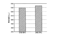
図12A及び図12Bは、搬送波群の進行波のパワーの調整を説明するための図である。図12A及び図12Bにおいて、横軸は、搬送波群の中心周波数を示し、縦軸は、搬送波群の進行波のパワー[W]を示している。なお、搬送波群の進行波のパワーは、吸収パワーと、搬送波群の反射波のパワーとの和に相当する。図12Aは、制御部100が、搬送波群生成部16を制御して、吸収パワーが閾値である2550W以上となるように、上記の「パラメータ」として、搬送波群の中心周波数を2438MHz又は2462MHzに調整した状態を示している。また、図12Bは、搬送波群の中心周波数を2438MHz又は2462MHzに調整した後に、搬送波群生成部16を制御して、吸収パワーが閾値以上の一定値である2750Wとなるように、搬送波群の進行波のパワーを調整した状態を示している。
12A and 12B are diagrams for explaining adjustment of the power of the traveling wave of the carrier wave group. 12A and 12B, the horizontal axis indicates the center frequency of the carrier group, and the vertical axis indicates the power [W] of the traveling wave of the carrier group. The power of the traveling wave of the carrier wave group is equivalent to the sum of the absorption power and the power of the reflected wave of the carrier wave group. FIG. 12A shows that the
図13A及び図13Bは、搬送波群の進行波のパワーの調整による効果を説明するための図である。図13A及び図13Bにおいて、横軸は、搬送波群の中心周波数を示し、縦軸は、搬送波群を用いて処理容器12内に生成されたプラズマの発光強度[a.u.]を示している。図13Aは、搬送波群の中心周波数が2438MHzに調整された場合のプラズマの発光強度と、搬送波群の中心周波数が2462MHzに調整された場合のプラズマの発光強度とを示している。また、図13Bは、搬送波群の中心周波数が2438MHzに調整された後に、吸収パワーが閾値以上の一定値である2750Wとなるように、搬送波群の進行波のパワーを調整した場合のプラズマの発光強度と、搬送波群の中心周波数が2462MHzに調整された後に、吸収パワーが閾値以上の一定値である2750Wとなるように、搬送波群の進行波のパワーを調整した場合のプラズマの発光強度とを示している。
FIGS. 13A and 13B are diagrams for explaining the effect of adjusting the power of the traveling wave of the carrier wave group. 13A and 13B, the horizontal axis represents the center frequency of the carrier wave group, and the vertical axis represents the emission intensity of the plasma generated in the
図13Aに示すように、搬送波群の進行波のパワーが調整されていない場合、中心周波数が2438MHzに調整された搬送波群に応じたプラズマの発光強度と、中心周波数が2462MHzに調整された搬送波群に応じたプラズマの発光強度との差が比較的に大きい。 As shown in FIG. 13A, when the power of the traveling wave of the carrier group is not adjusted, the emission intensity of the plasma corresponding to the carrier group whose center frequency is adjusted to 2438 MHz and the carrier group whose center frequency is adjusted to 2462 MHz The difference from the emission intensity of the plasma according to is relatively large.
これに対して、図13Bに示すように、搬送波群の進行波のパワーが調整された場合、中心周波数が2438MHzに調整された搬送波群に応じたプラズマの発光強度と、中心周波数が2462MHzに調整された搬送波群に応じたプラズマの発光強度との差が小さくなった。すなわち、吸収パワーが閾値以上の一定値である2750Wとなるように、搬送波群の進行波のパワーが調整されることによって、プラズマの発光強度の変動、言い換えると、プラズマ密度の変動が抑制されることが分かった。 On the other hand, as shown in FIG. 13B, when the power of the traveling wave of the carrier group is adjusted, the emission intensity of the plasma corresponding to the carrier group whose center frequency is adjusted to 2438 MHz, and the center frequency is adjusted to 2462 MHz. The difference with the emission intensity of plasma according to the set carrier wave group became small. That is, by adjusting the power of the traveling wave of the carrier wave group so that the absorption power becomes 2750 W which is a constant value equal to or greater than the threshold value, the fluctuation of the emission intensity of the plasma, in other words, the fluctuation of the plasma density is suppressed. I understood that.
1 プラズマ処理装置
12 処理容器
14 ステージ
16 搬送波群生成部
18 アンテナ
20 誘電体窓
30 スロット板
38 ガス供給系
100 制御部
101 コントローラ
102 ユーザインタフェース
103 記憶部DESCRIPTION OF
Claims (8)
所定の中心周波数を中心とする所定の周波数帯域に属する周波数であって、互いに異なる周波数をそれぞれ有する複数の搬送波から成る搬送波群を生成する搬送波群生成部と、
前記搬送波群を用いて、前記処理容器内にプラズマを生成するプラズマ生成部と、
前記搬送波群の進行波の周波数スペクトルである進行波スペクトルと、前記搬送波群の反射波の周波数スペクトルである反射波スペクトルとを検出するスペクトル検出部と、
前記進行波スペクトル及び前記反射波スペクトルを用いて、前記プラズマに吸収される前記搬送波群のパワーである吸収パワーを算出し、前記吸収パワーが閾値以上となるように、前記反射波スペクトルの極小値及び当該極小値に対応する周波数を変動させるパラメータを調整する制御部と
を有することを特徴とするプラズマ処理装置。A processing container,
A carrier belonging to a predetermined frequency band centered on a predetermined center frequency, a carrier group generation unit that generates a carrier group consisting of a plurality of carriers each having a different frequency,
Using the carrier wave group, a plasma generation unit that generates plasma in the processing container,
A traveling wave spectrum that is a frequency spectrum of a traveling wave of the carrier wave group, and a spectrum detection unit that detects a reflected wave spectrum that is a frequency spectrum of a reflected wave of the carrier wave group,
Using the traveling wave spectrum and the reflected wave spectrum, calculate the absorption power that is the power of the carrier wave group absorbed by the plasma, and calculate the minimum value of the reflected wave spectrum so that the absorption power is equal to or higher than a threshold value. And a control unit for adjusting a parameter for changing a frequency corresponding to the minimum value.
前記制御部は、前記チューナを制御して、前記パラメータとして前記可動部材の位置を掃引することによって、前記吸収パワーが前記閾値以上となる前記可動部材の位置を探索することを特徴とする請求項1又は2に記載のプラズマ処理装置。Including a movable movable member, according to the position of the movable member with respect to a reference position, further comprising a tuner to match the impedance between the carrier group generator and the processing container,
The control unit controls the tuner to sweep the position of the movable member as the parameter, thereby searching for a position of the movable member at which the absorbed power is equal to or greater than the threshold. 3. The plasma processing apparatus according to 1 or 2.
前記制御部は、前記反射波スペクトルの極小値に対応する周波数が前記処理容器内に異常放電を発生させない周波数の範囲を逸脱する場合に、警告を発することを特徴とする請求項4に記載のプラズマ処理装置。The frequency corresponding to the minimum value of the reflected wave spectrum, with the consumption of the processing container or the consumption of members in the processing container, changes with time,
The controller according to claim 4, wherein the control unit issues a warning when a frequency corresponding to a minimum value of the reflected wave spectrum deviates from a frequency range that does not cause abnormal discharge in the processing container. Plasma processing equipment.
所定の中心周波数を中心とする所定の周波数帯域に属する周波数であって、互いに異なる周波数をそれぞれ有する複数の搬送波から成る搬送波群を生成する搬送波群生成部と、
前記搬送波群を用いて、前記処理容器内にプラズマを生成するプラズマ生成部と、
前記搬送波群の進行波の周波数スペクトルである進行波スペクトルと、前記搬送波群の反射波の周波数スペクトルである反射波スペクトルとを検出するスペクトル検出部と
を有するプラズマ処理装置におけるプラズマ処理方法であって、
前記進行波スペクトルと前記反射波スペクトルとを用いて、前記プラズマに吸収される前記搬送波群のパワーである吸収パワーを算出し、
前記吸収パワーが閾値以上となるように、前記反射波スペクトルの極小値及び当該極小値に対応する周波数を変動させるパラメータを調整する
ことを特徴とするプラズマ処理方法。A processing container,
A carrier belonging to a predetermined frequency band centered on a predetermined center frequency, a carrier group generation unit that generates a carrier group consisting of a plurality of carriers each having a different frequency,
Using the carrier wave group, a plasma generation unit that generates plasma in the processing container,
A traveling wave spectrum that is a frequency spectrum of a traveling wave of the carrier wave group, and a spectrum detection unit that detects a reflected wave spectrum that is a frequency spectrum of a reflected wave of the carrier wave group. ,
Using the traveling wave spectrum and the reflected wave spectrum, calculate the absorption power that is the power of the carrier group absorbed by the plasma,
A plasma processing method, comprising: adjusting a minimum value of the reflected wave spectrum and a parameter for changing a frequency corresponding to the minimum value so that the absorption power is equal to or more than a threshold value.
Applications Claiming Priority (3)
| Application Number | Priority Date | Filing Date | Title |
|---|---|---|---|
| JP2015144345 | 2015-07-21 | ||
| JP2015144345 | 2015-07-21 | ||
| PCT/JP2016/071101 WO2017014210A1 (en) | 2015-07-21 | 2016-07-19 | Plasma processing device and plasma processing method |
Publications (2)
| Publication Number | Publication Date |
|---|---|
| JPWO2017014210A1 JPWO2017014210A1 (en) | 2018-05-10 |
| JP6665183B2 true JP6665183B2 (en) | 2020-03-13 |
Family
ID=57835183
Family Applications (1)
| Application Number | Title | Priority Date | Filing Date |
|---|---|---|---|
| JP2017529893A Active JP6665183B2 (en) | 2015-07-21 | 2016-07-19 | Plasma processing apparatus and plasma processing method |
Country Status (5)
| Country | Link |
|---|---|
| US (1) | US10622197B2 (en) |
| JP (1) | JP6665183B2 (en) |
| KR (1) | KR102553462B1 (en) |
| TW (1) | TWI685016B (en) |
| WO (1) | WO2017014210A1 (en) |
Families Citing this family (6)
| Publication number | Priority date | Publication date | Assignee | Title |
|---|---|---|---|---|
| CN110504149B (en) * | 2018-05-17 | 2022-04-22 | 北京北方华创微电子装备有限公司 | Pulse modulation system and method of radio frequency power supply |
| JP6846387B2 (en) * | 2018-06-22 | 2021-03-24 | 東京エレクトロン株式会社 | Plasma processing method and plasma processing equipment |
| US11901159B2 (en) | 2018-09-13 | 2024-02-13 | Hitachi Kokusai Electric Inc. | RF generator device and substrate processing apparatus |
| WO2020126175A1 (en) * | 2018-12-19 | 2020-06-25 | Evatec Ag | Vacuum system and method to deposit a compound layer |
| JP7122268B2 (en) * | 2019-02-05 | 2022-08-19 | 東京エレクトロン株式会社 | Plasma processing equipment |
| CN112992636B (en) * | 2019-12-17 | 2023-09-29 | 中微半导体设备(上海)股份有限公司 | RF power source device for plasma processing apparatus and RF power distribution method |
Family Cites Families (25)
| Publication number | Priority date | Publication date | Assignee | Title |
|---|---|---|---|---|
| JP3001658B2 (en) | 1991-03-28 | 2000-01-24 | 日本原子力研究所 | High frequency heating equipment |
| JP3544136B2 (en) | 1998-02-26 | 2004-07-21 | キヤノン株式会社 | Plasma processing apparatus and plasma processing method |
| JP5138131B2 (en) * | 2001-03-28 | 2013-02-06 | 忠弘 大見 | Microwave plasma process apparatus and plasma process control method |
| JP4024053B2 (en) * | 2002-02-08 | 2007-12-19 | キヤノンアネルバ株式会社 | High frequency plasma processing method and high frequency plasma processing apparatus |
| US7328126B2 (en) * | 2003-09-12 | 2008-02-05 | Tokyo Electron Limited | Method and system of diagnosing a processing system using adaptive multivariate analysis |
| US7127358B2 (en) * | 2004-03-30 | 2006-10-24 | Tokyo Electron Limited | Method and system for run-to-run control |
| JP4739793B2 (en) * | 2005-03-31 | 2011-08-03 | 株式会社ダイヘン | High frequency power supply |
| US7286948B1 (en) * | 2006-06-16 | 2007-10-23 | Applied Materials, Inc. | Method for determining plasma characteristics |
| JP5026916B2 (en) * | 2007-10-19 | 2012-09-19 | 株式会社日立ハイテクノロジーズ | Plasma processing equipment |
| US9196463B2 (en) * | 2011-04-07 | 2015-11-24 | Varian Semiconductor Equipment Associates, Inc. | System and method for plasma monitoring using microwaves |
| JP5847496B2 (en) * | 2011-09-01 | 2016-01-20 | 株式会社日立国際電気 | Plasma generation power supply apparatus and plasma generation parameter setting method |
| JP5935116B2 (en) * | 2011-12-16 | 2016-06-15 | 東京エレクトロン株式会社 | Plasma processing equipment |
| JP5943067B2 (en) * | 2012-03-26 | 2016-06-29 | 東京エレクトロン株式会社 | Plasma processing apparatus and high frequency generator |
| JP2014049362A (en) * | 2012-09-03 | 2014-03-17 | Tokyo Electron Ltd | Plasma generation device and substrate processing device |
| TW201438333A (en) * | 2013-03-20 | 2014-10-01 | Banner Technology Corp | Impedance matching method for plasma system |
| JP6374647B2 (en) * | 2013-11-05 | 2018-08-15 | 東京エレクトロン株式会社 | Plasma processing equipment |
| JP6353223B2 (en) * | 2013-12-20 | 2018-07-04 | 東京エレクトロン株式会社 | Plasma processing method and plasma processing apparatus |
| JP5819448B2 (en) * | 2014-01-06 | 2015-11-24 | 東京エレクトロン株式会社 | Plasma processing apparatus, abnormality determination method, and microwave generator |
| US10115567B2 (en) * | 2014-09-17 | 2018-10-30 | Tokyo Electron Limited | Plasma processing apparatus |
| US9977070B2 (en) * | 2014-10-21 | 2018-05-22 | Tokyo Electron Limited | Method for inspecting magnetron |
| TWI690972B (en) * | 2015-05-12 | 2020-04-11 | 日商東京威力科創股份有限公司 | Plasma processing device and plasma processing method |
| JP6643034B2 (en) * | 2015-10-09 | 2020-02-12 | 東京エレクトロン株式会社 | Plasma processing equipment |
| JP6754665B2 (en) * | 2016-10-18 | 2020-09-16 | 東京エレクトロン株式会社 | Microwave output device and plasma processing device |
| KR102520779B1 (en) * | 2016-11-18 | 2023-04-11 | 도쿄엘렉트론가부시키가이샤 | Compositional Emission Spectroscopy for Particle-Induced Arc Detection in Manufacturing Processes |
| JP6793019B2 (en) * | 2016-11-28 | 2020-12-02 | 東京エレクトロン株式会社 | Plasma processing equipment |
-
2016
- 2016-07-19 US US15/746,154 patent/US10622197B2/en active Active
- 2016-07-19 KR KR1020187001428A patent/KR102553462B1/en active IP Right Grant
- 2016-07-19 JP JP2017529893A patent/JP6665183B2/en active Active
- 2016-07-19 WO PCT/JP2016/071101 patent/WO2017014210A1/en active Application Filing
- 2016-07-20 TW TW105122943A patent/TWI685016B/en active
Also Published As
| Publication number | Publication date |
|---|---|
| TW201711082A (en) | 2017-03-16 |
| WO2017014210A1 (en) | 2017-01-26 |
| US10622197B2 (en) | 2020-04-14 |
| KR20180031680A (en) | 2018-03-28 |
| KR102553462B1 (en) | 2023-07-10 |
| JPWO2017014210A1 (en) | 2018-05-10 |
| TWI685016B (en) | 2020-02-11 |
| US20180211818A1 (en) | 2018-07-26 |
Similar Documents
| Publication | Publication Date | Title |
|---|---|---|
| JP6665183B2 (en) | Plasma processing apparatus and plasma processing method | |
| US9564296B2 (en) | Radial waveguide systems and methods for post-match control of microwaves | |
| JP6785936B2 (en) | Plasma processing equipment and plasma processing method | |
| JP6698033B2 (en) | Plasma processing apparatus and plasma processing method | |
| US9159536B2 (en) | Plasma processing apparatus, abnormal oscillation determination method and high-frequency generator | |
| WO2016002590A1 (en) | Plasma processing apparatus and plasma processing method | |
| JP5819448B2 (en) | Plasma processing apparatus, abnormality determination method, and microwave generator | |
| US10879045B2 (en) | Plasma processing apparatus | |
| JP2017204467A (en) | Plasma processing apparatus and plasma processing method | |
| US9659752B2 (en) | Method for presetting tuner of plasma processing apparatus and plasma processing apparatus | |
| JP6486207B2 (en) | Plasma processing equipment | |
| JP2016100312A (en) | Plasma processing device and plasma processing method |
Legal Events
| Date | Code | Title | Description |
|---|---|---|---|
| A621 | Written request for application examination |
Free format text: JAPANESE INTERMEDIATE CODE: A621 Effective date: 20190115 |
|
| TRDD | Decision of grant or rejection written | ||
| A01 | Written decision to grant a patent or to grant a registration (utility model) |
Free format text: JAPANESE INTERMEDIATE CODE: A01 Effective date: 20200121 |
|
| A61 | First payment of annual fees (during grant procedure) |
Free format text: JAPANESE INTERMEDIATE CODE: A61 Effective date: 20200219 |
|
| R150 | Certificate of patent or registration of utility model |
Ref document number: 6665183 Country of ref document: JP Free format text: JAPANESE INTERMEDIATE CODE: R150 |
|
| R250 | Receipt of annual fees |
Free format text: JAPANESE INTERMEDIATE CODE: R250 |
|
| R250 | Receipt of annual fees |
Free format text: JAPANESE INTERMEDIATE CODE: R250 |