JP6651908B2 - Liquid ejecting apparatus and method of manufacturing liquid ejecting apparatus - Google Patents
Liquid ejecting apparatus and method of manufacturing liquid ejecting apparatus Download PDFInfo
- Publication number
- JP6651908B2 JP6651908B2 JP2016041408A JP2016041408A JP6651908B2 JP 6651908 B2 JP6651908 B2 JP 6651908B2 JP 2016041408 A JP2016041408 A JP 2016041408A JP 2016041408 A JP2016041408 A JP 2016041408A JP 6651908 B2 JP6651908 B2 JP 6651908B2
- Authority
- JP
- Japan
- Prior art keywords
- wiring
- contact
- constant potential
- flow path
- metal
- Prior art date
- Legal status (The legal status is an assumption and is not a legal conclusion. Google has not performed a legal analysis and makes no representation as to the accuracy of the status listed.)
- Active
Links
- 239000007788 liquid Substances 0.000 title claims description 30
- 238000004519 manufacturing process Methods 0.000 title claims description 6
- 239000000758 substrate Substances 0.000 claims description 88
- 239000002184 metal Substances 0.000 claims description 41
- 239000000463 material Substances 0.000 claims description 29
- 238000005304 joining Methods 0.000 claims description 12
- 238000005520 cutting process Methods 0.000 claims description 7
- 238000007599 discharging Methods 0.000 claims description 4
- 238000000034 method Methods 0.000 claims description 4
- 239000000976 ink Substances 0.000 description 23
- 238000005530 etching Methods 0.000 description 13
- 230000008602 contraction Effects 0.000 description 7
- 238000001723 curing Methods 0.000 description 7
- 230000015572 biosynthetic process Effects 0.000 description 4
- 230000005684 electric field Effects 0.000 description 4
- 239000000853 adhesive Substances 0.000 description 3
- 230000001070 adhesive effect Effects 0.000 description 3
- 238000004891 communication Methods 0.000 description 3
- 230000007423 decrease Effects 0.000 description 3
- 230000005611 electricity Effects 0.000 description 3
- 239000003086 colorant Substances 0.000 description 2
- 239000004020 conductor Substances 0.000 description 2
- 230000000694 effects Effects 0.000 description 2
- 238000012986 modification Methods 0.000 description 2
- 230000004048 modification Effects 0.000 description 2
- 230000000149 penetrating effect Effects 0.000 description 2
- 230000002093 peripheral effect Effects 0.000 description 2
- 230000010287 polarization Effects 0.000 description 2
- 229910001220 stainless steel Inorganic materials 0.000 description 2
- 239000010935 stainless steel Substances 0.000 description 2
- 230000003068 static effect Effects 0.000 description 2
- 239000004642 Polyimide Substances 0.000 description 1
- 238000003491 array Methods 0.000 description 1
- 238000005452 bending Methods 0.000 description 1
- 230000015556 catabolic process Effects 0.000 description 1
- 239000013078 crystal Substances 0.000 description 1
- 238000010586 diagram Methods 0.000 description 1
- NKZSPGSOXYXWQA-UHFFFAOYSA-N dioxido(oxo)titanium;lead(2+) Chemical compound [Pb+2].[O-][Ti]([O-])=O NKZSPGSOXYXWQA-UHFFFAOYSA-N 0.000 description 1
- 230000014509 gene expression Effects 0.000 description 1
- 238000013007 heat curing Methods 0.000 description 1
- 238000002347 injection Methods 0.000 description 1
- 239000007924 injection Substances 0.000 description 1
- 238000010030 laminating Methods 0.000 description 1
- HFGPZNIAWCZYJU-UHFFFAOYSA-N lead zirconate titanate Chemical compound [O-2].[O-2].[O-2].[O-2].[O-2].[Ti+4].[Zr+4].[Pb+2] HFGPZNIAWCZYJU-UHFFFAOYSA-N 0.000 description 1
- 229910052451 lead zirconate titanate Inorganic materials 0.000 description 1
- 239000007769 metal material Substances 0.000 description 1
- 238000013508 migration Methods 0.000 description 1
- 230000005012 migration Effects 0.000 description 1
- 229920001721 polyimide Polymers 0.000 description 1
- 238000012545 processing Methods 0.000 description 1
- 229910000679 solder Inorganic materials 0.000 description 1
- 229920003002 synthetic resin Polymers 0.000 description 1
- 239000000057 synthetic resin Substances 0.000 description 1
- 238000005491 wire drawing Methods 0.000 description 1
Images


Landscapes
- Particle Formation And Scattering Control In Inkjet Printers (AREA)
Description
本発明は、液体吐出装置、及び、液体吐出装置の製造方法に関する。 The present invention relates to a liquid ejection device and a method for manufacturing a liquid ejection device.
特許文献1には、液体吐出装置として、インクを吐出するインクジェットヘッドが開示されている。このヘッドは、金属製の流路部材と、流路部材に配置された圧電アクチュエータと、圧電アクチュエータを覆うように配置され、且つ、圧電アクチュエータと電気的に接続された配線部材(FPC)とを有する。配線部材にはドライバICが設けられており、ドライバICから配線部材に形成された配線を介して、圧電アクチュエータへ駆動信号が出力される。 Patent Literature 1 discloses an ink jet head that discharges ink as a liquid discharge device. The head includes a metal flow path member, a piezoelectric actuator disposed in the flow path member, and a wiring member (FPC) disposed to cover the piezoelectric actuator and electrically connected to the piezoelectric actuator. Have. The wiring member is provided with a driver IC, and a driving signal is output from the driver IC to the piezoelectric actuator via wiring formed on the wiring member.
また、上記文献には、金属製の流路部材の電位をグランドに維持するための構成が開示されている。まず、配線部材には接地配線が形成されている。また、配線部材のフレキシブル基板には突出部が設けられ、この突出部には、接地配線と接続された延出部が形成されている。 Further, the above document discloses a configuration for maintaining the potential of a metal flow path member at the ground. First, a ground wiring is formed on the wiring member. Further, a protruding portion is provided on the flexible substrate of the wiring member, and the protruding portion has an extending portion connected to the ground wiring.
フレキシブル基板の突出部は流路部材の表面まで延びている。そして、突出部に形成された延出部と流路部材とが接触した状態で、突出部が流路部材に接着剤で固定されている。これにより、配線部材の接地配線と流路部材とが延出部を介して導通し、流路部材の電位がグランドに維持される。 The protrusion of the flexible substrate extends to the surface of the flow path member. The protruding portion is fixed to the flow channel member with an adhesive in a state where the extension formed on the protruding portion and the flow channel member are in contact with each other. Thereby, the ground wiring of the wiring member and the flow path member conduct through the extension portion, and the potential of the flow path member is maintained at the ground.
上記文献において、配線部材の突出部と流路部材とを硬化性接着剤で接合したときに、加熱硬化時の接着剤の収縮によって、配線部材に引っ張り力が作用する。これにより、配線部材と圧電アクチュエータとの電気接続部に、配線部材を引き剥がす方向の力がかかり、接続不良が生じる虞がある。しかし、この点に対する工夫については、上記文献には何も開示されていない。 In the above document, when the projecting portion of the wiring member and the flow path member are joined with a curable adhesive, a tensile force acts on the wiring member due to shrinkage of the adhesive during heat curing. As a result, a force in a direction in which the wiring member is peeled off is applied to the electrical connection between the wiring member and the piezoelectric actuator, and a connection failure may occur. However, the above document does not disclose anything about a device for this point.
本発明の目的は、流路部材と配線部材の定電位配線とを導通状態で接合する際に、接合材料の硬化収縮に起因する接続不良の発生を抑えることにある。 SUMMARY OF THE INVENTION An object of the present invention is to suppress the occurrence of a connection failure due to curing shrinkage of a bonding material when a flow path member and a constant potential wiring of a wiring member are connected in a conductive state.
本発明の液体吐出装置は、少なくとも一部が金属で形成された流路部材と、前記流路部材に配置されたエネルギー付与部とを有するヘッドユニットと、前記エネルギー付与部に対して前記流路部材と反対側に配置され、フレキシブル基板と、第1方向に配列されて前記エネルギー付与部と電気的に接続される複数の第1接点と、前記複数の第1接点から前記第1方向の一方側にそれぞれ引き出された複数の第1駆動配線と、前記第1方向と直交する第2方向において前記第1接点及び前記第1駆動配線よりも前記フレキシブル基板の縁側に配置され、且つ、一定電位が印加される第1定電位配線と、前記第2方向において一部の前記第1接点と前記第1定電位配線との間に配置され、前記第1接点とは接続されないダミー導電部と、を有する配線部材、を備え、前記第1定電位配線の前記第2方向において前記ダミー導電部に隣接する部分と、前記流路部材の金属部分、又は、前記流路部材の前記金属部分に設けられた前記金属製部材とを導通状態で接合する、硬化性接合材料からなる接合部を有することを特徴とするものである。 The liquid ejecting apparatus according to the present invention is a liquid ejection device, comprising: a head unit having a flow path member at least partially formed of metal; an energy applying unit disposed in the flow path member; A flexible substrate, a plurality of first contacts arranged in a first direction and electrically connected to the energy applying unit, and one of the plurality of first contacts in the first direction arranged on the opposite side to the member; A plurality of first drive wirings respectively drawn out to the side, and are arranged on the edge side of the flexible substrate with respect to the first contact and the first drive wirings in a second direction orthogonal to the first direction, and have a constant potential. A first constant potential wiring to which is applied, a dummy conductive portion disposed between some of the first contacts and the first constant potential wiring in the second direction, and not connected to the first contact; Having A line member, the first constant potential wiring being provided in a portion adjacent to the dummy conductive portion in the second direction in the second direction, a metal portion of the flow path member, or a metal portion of the flow path member. It has a joint made of a curable joining material for joining the metal member in a conductive state.
配線部材においては、第1方向に配列された複数の第1接点から、第1方向一方側に複数の第1駆動配線がそれぞれ引き出されている。このように、複数の接点から全て同じ方向に配線が引き出されている構成では、配線の引出側と反対側の接点近傍においては、駆動配線の数が少なくなる。ここで、フレキシブル基板に、配線密度が高い領域と低い領域とが存在すると、下記の問題が生じる虞がある。即ち、フレキシブル基板に形成した導電膜をエッチングして配線を形成する際に、配線密度が異なる2つの領域間では、エッチングの進行に大きな差が出る。具体的には、エッチング液の流速差が大きくなる。これにより、配線密度が高い領域の一部におけるエッチングが、配線密度が低い領域のエッチングの影響を受けて、エッチング精度が低下する。そこで、本発明では、フレキシブル基板上での配線密度の不均一を抑えるため、末端側に位置する第1接点の近くには、第1接点とは接続されないダミー導電部が形成されている。 In the wiring member, a plurality of first drive wires are respectively drawn out to one side in the first direction from a plurality of first contacts arranged in the first direction. As described above, in the configuration in which the wires are all drawn out from the plurality of contacts in the same direction, the number of drive wires is reduced in the vicinity of the contact opposite to the wire drawing side. Here, if the flexible substrate includes a region having a high wiring density and a region having a low wiring density, the following problem may occur. That is, when wiring is formed by etching a conductive film formed on a flexible substrate, there is a large difference in the progress of etching between two regions having different wiring densities. Specifically, the difference in the flow velocity of the etching liquid increases. As a result, etching in a part of the region where the wiring density is high is affected by etching in the region where the wiring density is low, and the etching accuracy is reduced. Therefore, in the present invention, a dummy conductive portion that is not connected to the first contact is formed near the first contact located on the terminal side in order to suppress uneven wiring density on the flexible substrate.
一方で、本発明では、流路部材の電位を一定電位に維持するため、フレキシブル基板に形成された第1定電位配線と、流路部材の金属部分、又は、流路部材の金属部分に設けられた金属製部が導通している。即ち、フレキシブル基板の縁側に配置された第1定電位配線と、前記金属部分又は前記金属製部材とが、硬化性接合材料によって導通状態で接合されている。その接合の際に、接合材料の硬化収縮によって、配線部材に引っ張り力が作用する。その引っ張り力は、フレキシブル基板自身の伸縮によってある程度は吸収できるのであるが、硬化性接合材料の接合部と第1接点との間に、多くの第1駆動配線が配置されていると、この部分の基板剛性が高くなり、基板による引っ張り力の吸収効果は低くなる。 On the other hand, in the present invention, in order to maintain the potential of the flow path member at a constant potential, the first constant potential wiring formed on the flexible substrate and the metal part of the flow path member or the metal part of the flow path member are provided. The metal part is conducting. That is, the first constant potential wiring arranged on the edge side of the flexible substrate and the metal portion or the metal member are joined in a conductive state by the curable joining material. At the time of the joining, a tensile force acts on the wiring member due to the curing shrinkage of the joining material. The tensile force can be absorbed to some extent by the expansion and contraction of the flexible substrate itself. However, if many first drive wirings are arranged between the joint of the curable joining material and the first contact, this portion is The rigidity of the substrate increases, and the effect of absorbing the tensile force by the substrate decreases.
この点、本発明では、フレキシブル基板の縁側に位置する第1定電位配線は、ダミー導電部と隣接する部分において、流路部材の金属部分と接合されている。つまり、硬化性接合材料の接合部と第1接点との間にダミー導電部が存在する。ダミー導電部は、第1駆動配線とは違って、第1接点とは接続されない導電パターンである。そのため、接合部と第1接点の間において、接合部から作用する引っ張り力が緩和されるように、ダミー導電部のパターンを任意に調整することが可能である。 In this regard, in the present invention, the first constant potential wiring located on the edge side of the flexible substrate is joined to the metal portion of the flow path member at a portion adjacent to the dummy conductive portion. That is, the dummy conductive portion exists between the bonding portion of the curable bonding material and the first contact. The dummy conductive portion is a conductive pattern that is not connected to the first contact unlike the first drive wiring. Therefore, it is possible to arbitrarily adjust the pattern of the dummy conductive portion so that the tensile force acting from the joint is reduced between the joint and the first contact.
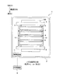
次に、本発明の実施の形態について説明する。図1は、本実施形態に係るプリンタの概略的な平面図である。尚、図1に示す前後左右の各方向をプリンタの「前」「後」「左」「右」と定義する。また、図1の紙面手前側を「上」、紙面向こう側を「下」とそれぞれ定義する。以下では、前後左右上下の各方向語を適宜使用して説明する。 Next, an embodiment of the present invention will be described. FIG. 1 is a schematic plan view of the printer according to the present embodiment. Note that the front, rear, left, and right directions shown in FIG. 1 are defined as “front”, “rear”, “left”, and “right” of the printer. 1 is defined as “upper”, and the other side of the paper is defined as “down”. In the following, description will be made by using the front, rear, left, right, upper, and lower direction words as appropriate.
<プリンタの概略構成>
図1に示すように、プリンタ1は、筐体2内に収容されたプラテン3、4つのインクジェットヘッド4、2つの搬送ローラ5,6、及び、制御装置7等を備えている。
<Schematic configuration of printer>
As shown in FIG. 1, the printer 1 includes a
プラテン3の上面には、記録媒体100が載置される。4つのインクジェットヘッド4は、プラテン3の上方において、搬送方向に並べて配置されている。各インクジェットヘッド4には、図示しないインクタンクからインクが供給される。尚、4つのインクジェットヘッド4には、異なる色のインクが供給される。つまり、4つのインクジェットヘッド4は、互いに異なる色のインクを吐出するものである。
The
4つのインクジェットヘッド4は同一の構造を有するため、そのうちの1つについて説明する。図2は、1つのインクジェットヘッド4の平面図である。図2に示すように、各インクジェットヘッド4は、左右に長い矩形板状のホルダ10と、このホルダ10に取り付けられた複数のヘッドユニット11を備えている。
Since the four
複数のヘッドユニット11は、搬送方向において前側と後側に交互に分かれて配置されている。また、前側に配置されたヘッドユニット11と後側に配置されたヘッドユニット11との間で、左右方向の位置がずれている。即ち、複数のヘッドユニット11は、左右方向に沿って、前後に千鳥状に分かれて配置されている。各ヘッドユニット11は、左右方向に並ぶ複数のノズル25を有する。また、複数のノズル25が配列されたプリンタ1の左右方向を、「ノズル配列方向」と呼ぶ。ヘッドユニット11の構成の詳細については後述する。
The plurality of
図1に示すように、2つの搬送ローラ5,6は、プラテン3に対して後側と前側にそれぞれ配置されている。2つの搬送ローラ5,6は、図示しないモータによってそれぞれ駆動され、プラテン3上の記録媒体100を前方へ搬送する。以下では、記録媒体100が搬送されるプリンタ1の前後方向を、「搬送方向」と呼ぶ。
As shown in FIG. 1, the two
制御装置7は、CPU(Central Processing Unit)、ROM(Read Only Memory)、RAM(Random Access Memory)、EEPROM(Electrically Erasable Programmable Read-Only Memory)などの不揮発性メモリ、及び、各種制御回路を含むASIC(Application Specific Integrated Circuit)を備える。また、制御装置7は、PC等の外部装置9とデータ通信可能に接続されており、外部装置9から送られた印刷データに基づいて、プリンタ1の各部を制御する。
The
より具体的には、制御装置7は、搬送ローラ5,6を駆動するモータを制御して、2つの搬送ローラ5,6に記録媒体100を搬送方向に搬送させる。また、これとともに、制御装置7は、4つのインクジェットヘッド4を制御して記録媒体100に向けてインクを吐出させる。これにより、記録媒体100に画像が印刷される。
More specifically, the
<ヘッドユニットの詳細構成>
次に、ヘッドユニット11及びその周辺の構成について詳細に説明する。図3はヘッドユニット11の斜視図、図4はヘッドユニット11の平面図、図5は図4のA部拡大図である。図6は図5のVI-VI線断面図、図7は図5のVII-VII線断面図である。
<Detailed configuration of head unit>
Next, the configuration of the
図3〜図7に示すように、ヘッドユニット11は、流路ユニット20と、圧電アクチュエータ21と、フレーム部材29とを備えている。また、圧電アクチュエータ21の上面には、COF(Chip On Film)60が接続されている。さらに、COF60は、FPC(Flexible Printed Circuit)75を介して、プリンタ1の制御装置7と接続されている。
As shown in FIGS. 3 to 7, the
尚、図4〜図7では、ヘッドユニット11の流路ユニット20と圧電アクチュエータ21の構成がわかりやすくなるように、フレーム部材29及びCOF60については、図示を省略、あるいは、二点鎖線で簡易的に示している。尚、図7では、図6においては示されている、圧力室26よりも下側の流路構造は省略されている。
In FIGS. 4 to 7, the
(流路ユニット)
図6に示すように、流路ユニット20は、それぞれ流路形成孔が形成された7枚の金属プレート31〜37が互いに積層されることによって形成されている。金属プレート31〜37は、例えば、ステンレス鋼のプレートである。7枚の金属プレート31〜37が積層されたときにそれぞれの流路形成孔が連通することによって、流路ユニット20には、以下のインク流路が形成されている。
(Channel unit)
As shown in FIG. 6, the
図4に示すように、流路ユニット20の上面には、搬送方向に並ぶ4つのインク供給孔23が形成されている。4つのインク供給孔23は1つのインクタンク(図示省略)と接続される。即ち、4つのインク供給孔23には同色のインクが供給される。流路ユニット20の内部には、4つのインク供給孔23にそれぞれ接続された4本のマニホールド24が形成されている。4本のマニホールド24は、それぞれ搬送方向に延在している。
As shown in FIG. 4, four ink supply holes 23 arranged in the transport direction are formed on the upper surface of the
また、流路ユニット20は、最下層のプレート37に形成された複数のノズル25と、最上層のプレート31に形成された複数の圧力室26を有する。図4に示すように、複数のノズル25は左右方向に沿って配列され、4本のマニホールド24にそれぞれ対応した4つのノズル列を構成している。尚、4つのノズル列の間では、ノズル25の位置は互いにずれている。より詳細には、各ノズル列におけるノズル配列ピッチをPとしたときに、4つのノズル列の間で、ノズル配列方向におけるノズル25の位置がP/4ずつずれている。
The
複数の圧力室26は、流路ユニット20の上面に沿って平面的に配置され、また、後述する圧電アクチュエータ21によって上方から覆われている。複数の圧力室26は、複数のノズル25の配列に従って配列され、搬送方向に並ぶ4つの圧力室列を構成している。各圧力室26は、対応するマニホールド24と、絞り流路27を介して連通している。一方で、各圧力室26は、対応するノズル25と、連通流路28を介して連通している。以上より、図6に示すように、流路ユニット20には、マニホールド24から分岐して、絞り流路27、圧力室26、及び、連通流路28を経てノズル25に至る、個別インク流路が複数形成されている。
The plurality of
尚、図6に示すように、最下層の金属プレート37の下面の外周領域には、ノズル25の形成領域を取り囲むように、金属で形成された枠状の接地部材38が固定されている。この接地部材38を介して、流路ユニット20は、プリンタ1のグランドと接続されている。
As shown in FIG. 6, a frame-shaped
(圧電アクチュエータ)
圧電アクチュエータ21は、流路ユニット20の上面に、複数の圧力室26を覆うように接合されている。圧電アクチュエータ21は、3枚の圧電層41〜43からなる圧電体40と、複数の個別電極44と、2種類の共通電極45,46を備えている。
(Piezoelectric actuator)
The
圧電体40を構成する3枚の圧電層41〜43は、それぞれ、チタン酸鉛とジルコン酸鉛との混晶であるチタン酸ジルコン酸鉛を主成分とする圧電材料からなる。圧電層41〜43は、互いに積層された状態で、複数の圧力室26を覆うように流路ユニット20の上面に平面的に配置されている。
Each of the three
図4〜図7に示すように、複数の個別電極44は、最上層の圧電層41の上面に、複数の圧力室26に対応して配置されている。高電位共通電極45は、最上層の圧電層41と中間層の圧電層42との間に配置されている。グランド共通電極46は、中間層の圧電層42と最下層の圧電層43との間に配置されている。後で説明するが、3種類の電極44,45,46には、COF60に実装されたドライバIC62(図3参照)によって所定の電位が印加される。
As shown in FIGS. 4 to 7, the plurality of
図4、図5に示すように、複数の個別電極44は、圧力室26の配列に従って配列され、搬送方向に並ぶ4つの個別電極列を構成している。各個別電極44は、圧電体40を挟んで、対応する圧力室26のほぼ全域と対向している。また、各個別電極44の搬送方向における一端部から接点49が引き出されている。複数の接点49は、個別電極44の配列に応じて配列されている。より詳細には、前側2つの個別電極44の列に対応した接点群と、後側2つの個別電極44の列に対応した接点群の、2つの接点群に分かれて配置されている。
As shown in FIGS. 4 and 5, the plurality of
図6に示すように、各接点49は、導電性のバンプ48によってCOF60の信号出力接点69(図8〜図10参照)と電気的に接続される。これにより、個別電極44がCOF60のドライバIC62と接続され、ドライバIC62によって、個別電極44の電位が所定の駆動電位とグランド電位との間で切り換えられる。尚、図3に示すように、COF60には左右2つのドライバIC62が実装されている。そして、圧電アクチュエータ21の複数の接点49のうち、左側に配置されている接点49aは左側のドライバIC62aと接続され、右側に配置されている接点49bは右側のドライバIC62bと接続される。
As shown in FIG. 6, each
高電位共通電極45は、圧電層41,42の間において、複数の圧力室26に跨って配置されている。図7に示すように、高電位共通電極45の1つの圧力室26に対応する部分は、圧力室26のノズル配列方向における中央部と対向している。
The high-potential
この高電位共通電極45に関し、図4に示すように、圧電層41の上面に2つの接続電極部51が形成されている。圧電層41の上面の左側領域においては後側の縁部に接続電極部51が配置され、圧電層41の上面の右側領域においては前側の縁部に接続電極部51が配置されている。これら2つの接続電極部51は、圧電層41を貫通する導通部53により、高電位共通電極45と導通している。また、2つの接続電極部51は、導電性のバンプ55によってCOF60の高電位配線71(図8参照)と電気的に接続される。これにより、高電位共通電極45には、常時、駆動電位が印加される。即ち、高電位共通電極45は、常に駆動電位に維持される定電位電極である。
Regarding the high-potential
グランド共通電極46は、圧電層42,43の間において、複数の圧力室26に跨って配置されている。図7に示すように、グランド共通電極46の1つの圧力室26に対応する部分は、圧力室26のノズル配列方向における両端部と対向している。
The ground
上記の高電位共通電極45と同様、グランド共通電極46についても、図4、図5に示すように、圧電層41の上面に2つの接続電極部52が形成されている。圧電層41の上面の左側領域においては前側の縁部に接続電極部52が配置され、圧電層41の上面の右側領域においては後側の縁部に接続電極部52が配置されている。これにより、圧電層41の前側縁部と後側縁部において、高電位共通電極45用の接続電極部51と、グランド共通電極46用の接続電極部52とが、ノズル配列方向において並んでいる。
Like the high-potential
2つの接続電極部52は、圧電層41を貫通する導通部54によって、グランド共通電極46と導通している。また、2つの接続電極部52は、導電性のバンプ56によって、COF60のグランド配線72(図8〜図10参照)と電気的に接続される。これにより、グランド共通電極46はCOF60のグランド配線72と接続される。即ち、グランド共通電極46は、常にグランドに維持される定電位電極である。
The two
図7に示すように、圧力室26のほぼ全域を覆う個別電極44は、ノズル配列方向における中央部において、高電位共通電極45と対向する。つまり、最上層の圧電層41の、圧力室26の中央部と対向する部分が、個別電極44と高電位共通電極45に挟まれている。圧電層41の、個別電極44と高電位共通電極45に挟まれた上記部分を第1活性部R1と呼ぶ。第1活性部R1は、圧電体40の厚み方向に分極されている。
As shown in FIG. 7, the
また、個別電極44は、ノズル配列方向における両端部において、グランド共通電極46と対向する。つまり、上側2枚の圧電層41,42の、圧力室26の両端部と対向する部分が、個別電極44とグランド共通電極46に挟まれている。以下、圧電層41,42の、個別電極44とグランド共通電極46に挟まれた上記部分を第2活性部R2と呼ぶ。第2活性部R2も、第1活性部R1と同様、圧電体40の厚み方向に分極されている。
The
次に、ドライバIC62によって個別電極44の電位が切り換えられたときの、圧電アクチュエータ21の動作について、図7を参照して説明する。
Next, the operation of the
個別電極44の電位がグランド電位である状態では、個別電極44と高電位共通電極45との間に電位差が生じて、第1活性部R1に、高電位共通電極45から個別電極44に向かう、厚み方向の電界が作用する。このとき、第1活性部R1に作用する電界の方向と分極方向とが平行となることから、第1活性部R1が厚み方向に延びて面方向に収縮する。圧力室26の中央部と対向する第1活性部R1の収縮により、圧電体40が圧力室26側に凸となるように撓んだ状態となる。尚、このとき、個別電極44とグランド共通電極46のグランド共通電極46の間には電位差が生じないことから、第2活性部R2には面方向の収縮は生じていない。
In a state where the potential of the
この状態から、個別電極44の電位が駆動電位に切り換えられると、個別電極44と高電位共通電極45との間に電位差がなくなり、第1活性部R1の収縮が解消される。これにより、圧電体40がほぼ平坦な状態となり、上記の個別電極44に駆動電位が印加されている場合と比べて圧力室26の容積が増加する。尚、個別電極44とグランド共通電極46との間においては逆に電位差が発生し、第2活性部R2には、個別電極44からグランド共通電極46に向かう電界が作用する。この電界の方向は第2活性部R2の分極方向と平行となることから、第2活性部R2は面方向に収縮することになる。
When the potential of the
このように、個別電極44の電位が駆動電位とグランド電位との間で切り換えられることで、圧力室26と対向する領域において圧電体40が上下に変位し、圧力室26の容積が変化する。この容積変化によって、圧力室26内のインクに圧力が付与され、圧力室26に連通するノズル25からインクが吐出される。
As described above, when the potential of the
(フレーム部材)
図3、図6に示すように、フレーム部材29は、矩形枠状の部材であり、流路ユニット20の上面の、圧電アクチュエータ21の周囲領域に接合される。このフレーム部材29により、流路ユニット20が補強される。フレーム部材29は、例えば、ステンレス鋼などの金属材料で形成され、流路ユニット20を構成する金属プレート31〜37よりも厚く、強度が高い。
(Frame member)
As shown in FIGS. 3 and 6, the
(COF)
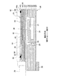
COF60は、左右方向に長い配線部材であり、図3、図4、図6に示すように、圧電アクチュエータ21の上方に配置されている。図8は、COF60の平面図である。図9は、図8のB部拡大図である。図10は、図9のCOF60とその下のヘッドユニット11のX-X線断面図である。尚、以下のCOF60の説明においては、左右方向を「基板長手方向」、前後方向を「基板短手方向」と定義し、適宜これらの表現を使用して説明を行う。
(COF)
The
図8に示すように、COF60は、フレキシブル基板61と、フレキシブル基板61に設けられた2つのドライバIC62と、フレキシブル基板61に形成された接点65,66,67,69及び配線68,70,71,72を有する。
As shown in FIG. 8, the
フレキシブル基板61は、ポリイミドなどの合成樹脂材料で形成された絶縁性のフィルムである。図3に示すように、フレキシブル基板61の、圧電アクチュエータ21から左右にはみ出した2つの部分63は、それぞれ上方へ折り返されている。上記2つの折り返し部分63には、2つのドライバIC62(62a,62b)がそれぞれ設けられ、2つのドライバIC62は、圧電アクチュエータ21の真上に配置されている。
The
フレキシブル基板61上の接点及び配線は、エッチングで形成される。即ち、フレキシブル基板61に全面的に導電膜を形成した後、この導電膜をエッチング液で部分的に除去することによって、各種の接点や配線を形成する。
The contacts and wiring on the
フレキシブル基板61の、基板長手方向における2つの端部の各々には、複数の信号入力接点65と、高電位入力接点66と、グランド入力接点67が、フレキシブル基板61の縁に沿って配置されている。信号入力接点65は、入力配線68によってドライバIC62と接続されている。高電位入力接点66とグランド入力接点67は、複数の信号入力接点65の前後両側に配置されている。尚、フレキシブル基板61の左端部においては、高電位入力接点66が後、グランド入力接点67が前に配置され、フレキシブル基板61の右端部においては、上とは逆で、高電位入力接点66が前、グランド入力接点67が後に配置されている。
At each of two ends of the
フレキシブル基板61の、2つのドライバIC62よりも基板長手方向の中央側には、複数の信号出力接点69が配置されている。複数の信号出力接点69は、圧電アクチュエータ21の複数の接点49の配列に対応して左右方向に配列され、前後2つの接点群に分かれて配置されている。
A plurality of
フレキシブル基板61の、基板長手方向における中心線Cよりも左側部分においては、複数の信号出力接点69aから複数の駆動配線70がそれぞれ左方へ引き出され、左側のドライバIC62aと接続されている。また、フレキシブル基板61の、中心線Cよりも右側部分においては、複数の信号出力接点69bから複数の駆動配線70がそれぞれ右方へ引き出され、右側のドライバIC62bと接続されている。
In a portion of the
フレキシブル基板61の、基板短手方向において、複数の信号出力接点69及び複数の駆動配線70よりも縁側の領域には、高電位配線71とグランド配線72が配置されている。フレキシブル基板61の左側部分においては、後側の縁に沿って、高電位入力接点66からフレキシブル基板61の中央部まで、高電位配線71が延びている。また、前側の縁に沿って、グランド入力接点67からフレキシブル基板61の中央部まで、グランド配線72が延びている。一方、フレキシブル基板61の右側部分では、上記とは配線71,72の前後配置が逆になっている。即ち、前側の縁に沿って高電位配線71が延び、後側の縁に沿ってグランド配線72が延びている。
A high-
言い換えれば、フレキシブル基板61の前側の縁部においては、左側のグランド配線72と右側の高電位配線71が、基板長手方向に並んでいる。また、後側の縁部においては、左側の高電位配線71と右側のグランド配線72とが、基板長手方向に並んでいる。高電位配線71の先端側部分は、導電性のバンプ55により、圧電アクチュエータ21の、高電位共通電極45の接続電極部51と接続される。同じく、グランド配線72の先端側部分は、導電性のバンプ56により、グランド共通電極46の接続電極部52と接続される。また、高電位配線71とグランド配線72は、それぞれ、ドライバIC62にも接続されている。
In other words, at the front edge of the
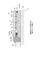
ところで、上述したように、フレキシブル基板61の左側部分では、全ての信号出力接点69aから駆動配線70が左方へ引き出され、右側部分では、全ての信号出力接点69bから駆動配線70が右方へ引き出されている。このように、多くの信号出力接点69から同じ方向に駆動配線70が引き出されている構成では、配線引出側と反対側、即ち、フレキシブル基板61の中心線C付近においては、駆動配線70の数が少なくなる。
By the way, as described above, in the left part of the
ここで、上述したように、フレキシブル基板61上の配線や接点は、基板61に全面的に形成した導電膜をエッチングすることによって形成する。その際に、フレキシブル基板61上で配線密度が高い領域と低い領域とが存在すると、下記の問題が生じる虞がある。即ち、フレキシブル基板61上の導電膜をエッチングして配線を形成する際に、配線密度が異なる2つの領域間では、エッチングの進行状況が大きな差が出る。具体的には、エッチング液の流速差が大きくなる。これにより、配線密度が高い領域の一部におけるエッチングが、配線密度が低い領域のエッチングの影響を受けてエッチング精度が低下し、狭ピッチの高精細な配線形成に支障が生じる。
Here, as described above, the wirings and contacts on the
そこで、本実施形態では、フレキシブル基板61上での配線密度の不均一を抑えるため、フレキシブル基板61の中央部、即ち、配線引出側と反対側の信号出力接点69の近くに、複数のダミー導電部73が形成されている。各ダミー導電部73は、信号出力接点69、高電位配線71、あるいは、グランド配線72とは接続されない、孤立した配線パターンである。また、駆動配線70が、信号出力接点69の近傍で、基板長手方向に対して傾斜した方向に延びているのに対して、各ダミー導電部73は、基板長手方向と平行に延びている。
Therefore, in the present embodiment, in order to suppress uneven wiring density on the
また、ダミー導電部73の配置領域においては、駆動配線70の配置領域と比べて、単位面積当たりの導電膜面積が小さくなっている。つまり、駆動配線70の配置領域の方が、基板上にある導電材料の量が多い。具体的には、ダミー導電部73の基板短手方向における配置間隔が、駆動配線70の配置間隔よりも大きくなっている。このような構成が採用されている理由については、後で説明する。
Further, in the arrangement region of the dummy
尚、図8では図示が省略されているが、配線68,70とダミー導電部73は、これらを保護するための絶縁膜74(例えば、ソルダーレジスト)で覆われている。但し、圧電アクチュエータ21あるいはFPC75と電気的接続が行われる、接点65,66,67,69、高電位配線71、及び、グランド配線72は、絶縁膜74から露出している。
Although not shown in FIG. 8, the
図3に示すように、圧電アクチュエータ21の上方に折り返された、COF60の左右2つの折り返し部分63には、FPC(Flexible Printed Circuit)75が接合されている。これにより、2つの折り返し部分63の端部に形成された複数の入力接点65,66,67と、FPC75とが電気的に接続されている。FPC75は、COF60の2つの折り返し部分63の上面から後方に延び、さらに、上方へ折り曲げられて、プリンタ1の制御装置7(図1参照)に接続されている。
As shown in FIG. 3, an FPC (Flexible Printed Circuit) 75 is joined to two left and right folded
(COFのグランド配線と流路ユニットとの導通)
ところで、プリンタ1の動作中に、静電気等によって金属で形成されている流路ユニット20に電荷が溜まると、インクの一部が帯電する。インクの帯電は、圧電アクチュエータ21においてマイグレーションの発生要因となり、絶縁破壊を引き起こす虞がある。また、ノズル25から吐出される液滴が帯電することにより、吐出曲がりの原因ともなる。
(Conduction between ground wiring of COF and flow path unit)
By the way, during the operation of the printer 1, when electric charges accumulate in the
そこで、図5に示すように、本実施形態の流路ユニット20は、接地部材38を介してプリンタ1のグランドと接続されている。しかしながら、多数の印刷媒体100への印刷を、高速且つ連続で行うプリンタにおいては、静電気による流路ユニット20の帯電の頻度が高く、上記構成だけでは帯電防止対策は十分とは言えない。そこで、本実施形態では、流路ユニット20のグランドの維持をより確実なものとするため、流路ユニット20の上面が、COF60のグランド配線72とも導通した構成となっている。
Therefore, as shown in FIG. 5, the
図8に示すように、基板長手方向に配列された複数の信号出力接点69のうち、中心線C側に位置する一部の信号出力接点69と、グランド配線72との間に、ダミー導電部73が配置されている。そして、フレキシブル基板61の前側の縁部に形成されたグランド配線72の、上記ダミー導電部73と隣接する部分に、基板短手方向外側に突出する突出部72aが形成されている。
As shown in FIG. 8, of the plurality of
図9に示すように、上記の突出部72aは、グランド配線72の、高電位配線71側の端から左側に所定距離L(例えば、5mm程度)離れた部分に形成されている。また、この突出部72aの先端は、フレキシブル基板61の、基板短手方向の端面において露出している。
As shown in FIG. 9, the protruding
上記の突出部72aを有するCOF60は次のようにして形成する。図11は、COF60の基板切断工程を説明する図である。COF60は、フレキシブル基板61となるリールテープ77に配線70,71,73等のパターンを形成したのち、このテープ77を所定サイズに切断することにより製造する。ここで、図11に示すように、配線形成工程では、グランド配線72のダミー導電部73と隣接する部分に、少し長めに突出した部分78を形成する。そして、次の切断工程で、上記の突出した部分78を分断するようにテープ77を切断する。これにより、図9に示すように、グランド配線72の突出部72aを、フレキシブル基板61の端面において露出させる。
The
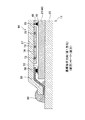
上記のCOF60をヘッドユニット11に接合する際には、まず、COF60の信号出力接点69、高電位配線71、及び、グランド配線72を、圧電アクチュエータ21の接点49、接続電極部51、及び、接続電極部52と、導電性のバンプ48,55,56を介して接合する。次に、図3、図10に示すように、COF60のフレキシブル基板61の前側の縁部と、流路ユニット20の上面との間に、導電性を有する液状の硬化性接合材料を注入した後、加熱して硬化させる。これにより、フレキシブル基板61の縁部に配置されたグランド配線72の突出部72aと、流路ユニット20の上面とが、導電性の硬化性接合材料からなる接合部79によって導通状態で接合される。この導通により、金属の流路ユニット20の電位が、確実に、グランド電位に維持される。
When joining the
図10に示すように、流路ユニット20の外周部にはフレーム部材29が接合されており、硬化性接合材料は、フレーム部材29と圧電アクチュエータ21との間の凹みに注入される。そのため、硬化前の液状の接合材料が、流路ユニット20の表面から垂れ落ちにくい。
As shown in FIG. 10, a
尚、COF60の前後2つの縁部のグランド配線72のうちの、何れのグランド配線72を流路ユニット20に接合してもよい。また、2つのグランド配線72の両方が流路ユニット20に接合されてもよい。但し、本実施形態では、図3に示すように、COF60の折り返し部分63の上面に接合されたFPC75が、後方へ引き出されている。そのため、FPC75をCOF60に接合した後に、グランド配線72と流路ユニット20との導通を行う場合は、前側のグランド配線72を流路ユニット20と導通させる方が、硬化性接合材料の注入等の作業を行いやすい。
In addition, any of the ground wirings 72 at the two front and rear edges of the
ところで、COF60のグランド配線72と流路ユニット20とを、硬化性接合材料で接合したときに、接合材料の硬化収縮によって、図10に矢印で示すように、COF60に引っ張り力が作用する。その引っ張り力は、フレキシブル基板61自身の伸縮によってある程度は吸収できる。しかし、接合部79と信号出力接点69との間に、多くの駆動配線70が配置されていると、この部分の基板剛性が高くなり、フレキシブル基板61自身による引っ張り力の吸収効果は低くなる。
By the way, when the
この点、本実施形態では、フレキシブル基板61の縁側に位置するグランド配線72は、ダミー導電部73と隣接する突出部72aにおいて、金属の流路ユニット20と接合されている。つまり、硬化性接合材料の接合部79と信号出力接点69との間にダミー導電部73が存在する。ここで、ダミー導電部73は、駆動配線70とは違って、信号出力接点69とは接続されない導電パターンである。そのため、接合部79と信号出力接点69の間において、接合部79から作用する引っ張り力が緩和されるように、ダミー導電部73のパターンを任意に調整することが可能である。
In this regard, in the present embodiment, the
また、フレキシブル基板61上の導電膜面積が少ないほど、フレキシブル基板61が伸縮しやすくなる。そこで、本実施形態では、ダミー導電部73の形成領域の導電膜面積が、駆動配線70の形成領域よりも小さくなっている。より具体的には、ダミー導電部73の配置間隔が、駆動配線70の配置間隔よりも大きくなっている。これにより、硬化時の接合部79の収縮によって生じる引っ張り力を、ダミー導電部73の形成領域で吸収しやすくなる。
In addition, the smaller the conductive film area on the
また、接合部79の硬化収縮による引っ張り力は、図10に示すように基板短手方向に作用する。この点、本実施形態では、各々のダミー導電部73は、基板長手方向に延びているため、ダミー導電部73によって、基板61の伸縮が阻害されにくい。
Further, the tensile force due to the curing shrinkage of the
グランド配線72の突出部72aが、フレキシブル基板61の端面において露出しているため、導電性の接合材料によって、COF60のグランド配線72と流路ユニット20とを導通させやすくなる。
Since the protruding
本実施形態では、フレキシブル基板61の左側部分では、信号出力接点69から駆動配線70が左方に引き出され、右側部分では信号出力接点69から駆動配線70が右方へ引き出されている。この構成では、左側部分と右側部分の境界付近、即ち、フレキシブル基板61の中心線C付近で、駆動配線70の数が少なくなり、逆に、ダミー導電部73の形成領域は増える。そのため、接合部79の硬化収縮による引っ張り力を、ダミー導電部73の形成領域で吸収するという観点では、フレキシブル基板61の中心線C付近に、接合部79が設けられるのがよい。
In the present embodiment, at the left side of the
しかし、本実施形態では、基板長手方向においてグランド配線72と隣接する位置まで、高い電位が印加される高電位配線71が配置されている。そのため、グランド配線72の、フレキシブル基板61の中心線Cに近い端部で流路ユニット20との導通を行うと、導電性の接合材料が流れ出して、グランド配線72と高電位配線71とがショートする虞がある。そこで、図9に示すように、グランド配線72の、高電位配線71側の端から所定距離Lだけ離れた部分において、接合部79による導通がなされている。
However, in the present embodiment, the high-
以上説明した実施形態において、インクジェットヘッド4が、本発明の「液体吐出装置」に相当する。COF60が、本発明の「配線部材」に相当する。流路ユニット20が、本発明の「流路部材」に相当する。圧電アクチュエータ21が、本発明の「エネルギー付与部」に相当する。基板長手方向が、本発明の「第1方向」に相当し、基板短手方向が、本発明の「第2方向」に相当する。フレキシブル基板61の左側に配置された信号出力接点69aが、本発明の「第1接点」に相当し、この信号出力接点69aに接続された駆動配線70が、本発明の「第1駆動配線70」に相当する。フレキシブル基板61の右側に配置された信号出力接点69bが、本発明の「第2接点」に相当し、この信号出力接点69bに接続された駆動配線70が、本発明の「第2駆動配線70」に相当する。グランド配線72が、本発明の「第1定電位配線」に相当し、高電位配線71が、本発明の「第2定電位配線」に相当する。
In the embodiment described above, the
次に、前記実施形態に種々の変更を加えた変更形態について説明する。但し、前記実施形態と同様の構成を有するものについては、同じ符号を付して適宜その説明を省略する。 Next, modified embodiments in which various changes are made to the above-described embodiment will be described. However, the components having the same configuration as the above embodiment are denoted by the same reference numerals, and the description thereof will be appropriately omitted.
1]ダミー導電部のパターンは、前記実施形態の図8で示したようなパターンには限られない。例えば、ダミー導電部の厚みが、駆動配線の厚みよりも薄くてもよい。また、1本のダミー導電部の幅が、駆動配線の幅よりも細くてもよい。あるいは、ダミー導電部が基板短手方向に延びていてもよい。 1] The pattern of the dummy conductive portion is not limited to the pattern as shown in FIG. For example, the thickness of the dummy conductive portion may be smaller than the thickness of the drive wiring. Further, the width of one dummy conductive portion may be smaller than the width of the drive wiring. Alternatively, the dummy conductive portion may extend in the lateral direction of the substrate.
2]硬化性接合材料を用いて、COF60のグランド配線72と流路ユニット20とを接合する際に、多量の接合材料が、COF60と流路ユニット20との間に流れ込むと、接合材料が硬化したときにフレキシブル基板61に作用する引っ張り力が大きくなる。そこで、図12、図13に示すように、グランド配線72に、硬化性接合材料が内側に流れ込むのを防ぐ、凸部80が形成されてもよい。図12、図13では、駆動配線70を覆う絶縁膜74の一部が、フレキシブル基板61の基板短手方向における縁部にも形成されている。この絶縁膜74の一部が、グランド配線72の突出部72aの、バンプ56よりも外側の領域を横切るように配置されることで、突出部72aの上に、基板長手方向に延びる帯状の凸部80が形成されている。
2] When a large amount of bonding material flows between the
3]前記実施形態の圧電アクチュエータ21は、複数の個別電極44と、駆動電位が印加される高電位共通電極45と、グランド電位が印加されるグランド共通電極46の2つの共通電極を有するものである。これに対して、複数の個別電極と、グランド電位が印加される共通電極のみを有する圧電アクチュエータも一般的に存在する。このような圧電アクチュエータに接続されるCOFにおいては、高電位配線が不要となる。
3] The
図14に示すCOF90は、左右2つのドライバIC62を有する点で、前記実施形態の図8と同じである。但し、高電位配線は存在せず、フレキシブル基板61の縁部においては、左端から右端までグランド配線92が延びている。即ち、このCOF90では、グランド配線92は、左側のドライバIC62aに接続される左側の信号出力接点69と隣接する領域から、右側のドライバIC62bに接続される右側の信号出力接点69と隣接する領域まで、基板長手方向に延びている。
The
図14の構成では、前記実施形態とは異なり、左側の信号出力接点69と右側の信号出力接点69の境界部、即ち、フレキシブル基板61の中心線C付近で、グランド配線92が高電位配線と近接しているわけではない。そのため、図14では、グランド配線92の、左右の接点69の境界部と隣接する部分、即ち、フレキシブル基板61の中心線Cの近傍部分に突出部92aが設けられ、突出部92aが、接合部79により流路ユニット20と接合されている。上記中心線C付近は、ダミー導電部73が最も多く配置される領域であることから、接合材料の硬化収縮による引っ張り力を効果的に吸収できる。
In the configuration of FIG. 14, unlike the above-described embodiment, the
4]フレキシブル基板に実装されるドライバICの数は2つには限られない。例えば、図15のCOF93では、フレキシブル基板94に、1つのドライバIC62が設けられている。尚、この形態では、信号出力接点69からの駆動配線70の引出とは反対側の、図中右側の縁部において、グランド配線95と流路ユニット20とが接合部79で接合されている。
4) The number of driver ICs mounted on the flexible substrate is not limited to two. For example, in the
5]接合部となる硬化性接合材料は、導電性のものには限られず、絶縁性の接合材料であってもよい。図16のCOF96では、フレキシブル基板97の縁部が流路ユニット20の上面まで垂れており、グランド配線98の一部が流路ユニット20の上面に直接接触して導通している。この状態で、グランド配線98の接触箇所の周囲に絶縁性の硬化性接合材料が注入されて硬化した接合部99により、グランド配線98と流路ユニット20の上面とが接合されている。
5] The curable bonding material to be the bonding portion is not limited to a conductive material, and may be an insulating bonding material. In the
6]前記実施形態では、流路ユニット20を構成するプレート31〜37が全て金属製のプレートであったが、流路ユニットの全体が金属で形成されている必要はない。即ち、流路ユニットのうちの、少なくとも、COFのグランド配線と接合部によって接合される部分が金属で形成されていればよい。
6] In the above embodiment, the
また、COFのグランド配線が、流路ユニットと直接接合されることも必須ではない。例えば、図10において、流路ユニット20と、この上面に固定されている金属製のフレーム部材29とが導通している場合に、COF60のグランド配線72が、流路ユニット20の代わりに、フレーム部材29と導通状態で接合されていてもよい。この場合、金属製のフレーム部材29が、本発明の「金属製部材」に相当する。
Further, it is not essential that the ground wiring of the COF is directly joined to the channel unit. For example, in FIG. 10, when the
以上説明した実施形態は、本発明を、記録用紙にインクを吐出して画像等を印刷するインクジェットヘッドに適用したものであるが、画像等の印刷以外の様々な用途で使用される液体吐出装置においても本発明は適用されうる。例えば、基板に導電性の液体を吐出して、基板表面に導電パターンを形成する液体吐出装置にも、本発明を適用することは可能である。 In the embodiments described above, the present invention is applied to an ink jet head that prints an image or the like by discharging ink on a recording sheet, but a liquid discharge device used in various applications other than printing of an image or the like. The present invention can also be applied to For example, the present invention can be applied to a liquid discharge device that discharges a conductive liquid to a substrate and forms a conductive pattern on the substrate surface.
4 インクジェットヘッド
11 ヘッドユニット
20 流路ユニット
21 圧電アクチュエータ
60 COF
61 フレキシブル基板
69 信号出力接点
70 駆動配線
71 高電位配線
72 グランド配線
72a 突出部
73 ダミー導電部
77 リールテープ
79 接合部
80 凸部(絶縁膜)
92 グランド配線
92a 突出部
94 フレキシブル基板
95 グランド配線
97 フレキシブル基板
98 グランド配線
99 接合部
4
61
92
Claims (10)
前記エネルギー付与部に対して前記流路部材と反対側に配置され、フレキシブル基板と、第1方向に配列されて前記エネルギー付与部と電気的に接続される複数の第1接点と、前記複数の第1接点から前記第1方向の一方側にそれぞれ引き出された複数の第1駆動配線と、前記第1方向と直交する第2方向において前記第1接点及び前記第1駆動配線よりも前記フレキシブル基板の縁側に配置され、且つ、一定電位が印加される第1定電位配線と、前記第2方向において一部の前記第1接点と前記第1定電位配線との間に配置され、前記第1接点とは接続されないダミー導電部と、を有する配線部材、を備え、
前記第1定電位配線の前記第2方向において前記ダミー導電部に隣接する部分と、前記流路部材の金属部分、又は、前記流路部材の前記金属部分に設けられた金属製部材とを導通状態で接合する、硬化性接合材料からなる接合部を有することを特徴とする液体吐出装置。 A flow path member at least partially formed of metal, and a head unit having an energy applying unit disposed in the flow path member,
A plurality of first contacts arranged on a side opposite to the flow path member with respect to the energy applying unit, arranged in a first direction, and electrically connected to the energy applying unit; A plurality of first drive wirings respectively drawn out from a first contact to one side in the first direction; and the flexible substrate more than the first contact and the first drive wiring in a second direction orthogonal to the first direction. And a first constant potential wiring to which a constant potential is applied, and a first constant potential wiring disposed between a part of the first contact and the first constant potential wiring in the second direction. A wiring member having a dummy conductive portion that is not connected to the contact,
Conducting a portion of the first constant potential wiring adjacent to the dummy conductive portion in the second direction and a metal part of the flow path member or a metal member provided on the metal part of the flow path member. A liquid ejecting apparatus having a joint made of a curable joining material, which is joined in a state.
前記第1接点よりも前記第1方向の他方側に配置された第2接点と、
前記第2接点から前記第1方向の前記他方側に引き出された第2駆動配線と、
前記第1定電位配線と前記第1方向に並び、且つ、前記第2接点とも前記第2方向に並び、前記第1定電位配線よりも高い電位が印加された第2定電位配線と、を有し、
前記第1定電位配線の、前記第2定電位配線側の端から前記第1方向の前記一方側に所定距離離れた部分が、前記接合部によって、前記流路部材の前記金属部分、又は、前記金属製部材と接合されていることを特徴とする請求項4又は5に記載の液体吐出装置。 The wiring member,
A second contact arranged on the other side of the first direction with respect to the first contact;
A second drive wiring extending from the second contact to the other side in the first direction;
A second constant potential line arranged in the first direction with the first constant potential line, and the second contact is also arranged in the second direction, and a higher potential than the first constant potential line is applied; Have
A portion of the first constant potential wiring, which is separated from the end on the second constant potential wiring side to the one side in the first direction by a predetermined distance, is formed by the joining portion, the metal portion of the flow path member, or The liquid ejection device according to claim 4, wherein the liquid ejection device is joined to the metal member.
前記第1接点よりも前記第1方向の他方側に配置された第2接点と、
前記第2接点から前記第1方向の前記他方側に引き出された第2駆動配線を有し、
前記第1定電位配線は、前記第2方向において前記第1接点と隣接する領域から、前記第2接点と隣接する領域まで、前記第1方向に延びており、
前記第1定電位配線の、前記第2方向において、前記第1接点と前記第2接点との境界部と隣接する部分が、前記接合部によって、前記流路部材の前記金属部分、又は、前記金属製部材と接合されていることを特徴とする請求項4又は5に記載の液体吐出装置。 The wiring member,
A second contact arranged on the other side of the first direction with respect to the first contact;
A second drive wiring extending from the second contact to the other side in the first direction;
The first constant potential wiring extends in the first direction from a region adjacent to the first contact in the second direction to a region adjacent to the second contact,
A portion of the first constant potential wiring, which is adjacent to a boundary portion between the first contact and the second contact in the second direction, is connected to the metal portion of the flow path member by the joining portion, or The liquid discharging device according to claim 4, wherein the liquid discharging device is joined to a metal member.
前記第1定電位配線の前記ダミー導電部に隣接する部分の少なくとも一部が、前記絶縁膜に覆われていることを特徴とする請求項1〜7の何れかに記載の液体吐出装置。 The wiring member has an insulating film covering the first drive wiring,
The liquid discharge device according to claim 1, wherein at least a part of a portion of the first constant potential wiring adjacent to the dummy conductive portion is covered with the insulating film.
前記エネルギー付与部に対して前記流路部材と反対側に配置され、フレキシブル基板と、第1方向に配列された複数の第1接点と、前記複数の第1接点から前記第1方向の一方側にそれぞれ引き出された複数の第1駆動配線と、前記第1方向と直交する第2方向において前記第1接点及び前記第1駆動配線よりも前記フレキシブル基板の縁側に配置され、且つ、一定電位が印加される第1定電位配線と、前記第2方向において一部の前記第1接点と前記第1駆動配線との間に配置され、前記第1接点とは接続されないダミー導電部を有する配線部材と、を備えた液体吐出装置の製造方法であって、
前記配線部材の前記第1接点を前記エネルギー付与部と電気的に接続する、接点接続工程と、
前記接点接続工程の後で、前記第2方向において前記第1定電位配線の前記ダミー導電部に隣接する部分と、前記流路部材の金属部分、又は、前記流路部材の前記金属部分に設けられた金属製部材との間に液状の硬化性接合材料を注入してから硬化させ、前記第1定電位配線と前記金属部分又は前記金属製部材とを導通させる、導通工程と、
を備えていることを特徴とする液体吐出装置の製造方法。 A flow path member at least partially formed of metal, and a head unit having an energy applying unit disposed in the flow path member,
The flexible substrate, a plurality of first contacts arranged in a first direction, and one side of the plurality of first contacts in the first direction with respect to the energy applying unit. And a plurality of first drive wirings respectively drawn out from the first contact and the first drive wiring in a second direction orthogonal to the first direction, which are arranged closer to the edge of the flexible substrate than the first drive wiring, and have a constant potential. A wiring member having a first constant potential wiring to be applied and a dummy conductive portion disposed between some of the first contacts and the first drive wiring in the second direction and not connected to the first contact; And a method for manufacturing a liquid ejection device comprising:
A contact connecting step of electrically connecting the first contact of the wiring member to the energy applying unit;
After the contact connection step, the first constant potential wiring is provided on the portion adjacent to the dummy conductive portion in the second direction, on the metal portion of the flow path member, or on the metal portion of the flow path member. Injecting a liquid curable bonding material between the metal member and the cured, and hardening, to conduct the first constant potential wiring and the metal portion or the metal member, a conduction step,
A method for manufacturing a liquid ejecting apparatus, comprising:
前記フレキシブル基板に、前記第1駆動配線、前記第1定電位配線、及び、前記ダミー導電部を形成する配線形成工程と、
前記フレキシブル基板を切断する切断工程と、を備え、
前記切断工程では、前記第2方向において前記第1定電位配線の前記ダミー導電部に隣接する部分を分断するように前記フレキシブル基板を切断し、前記フレキシブル基板の端面において前記第1定電位配線を露出させることを特徴とする請求項9に記載の液体吐出装置の製造方法。 The manufacturing process of the wiring member,
A wiring forming step of forming the first drive wiring, the first constant potential wiring, and the dummy conductive portion on the flexible substrate;
And a cutting step of cutting the flexible substrate,
In the cutting step, the flexible substrate is cut so as to divide a portion of the first constant potential wiring adjacent to the dummy conductive portion in the second direction, and the first constant potential wiring is cut at an end surface of the flexible substrate. The method for manufacturing a liquid ejection device according to claim 9, wherein the liquid ejection device is exposed.
Priority Applications (1)
| Application Number | Priority Date | Filing Date | Title |
|---|---|---|---|
| JP2016041408A JP6651908B2 (en) | 2016-03-03 | 2016-03-03 | Liquid ejecting apparatus and method of manufacturing liquid ejecting apparatus |
Applications Claiming Priority (1)
| Application Number | Priority Date | Filing Date | Title |
|---|---|---|---|
| JP2016041408A JP6651908B2 (en) | 2016-03-03 | 2016-03-03 | Liquid ejecting apparatus and method of manufacturing liquid ejecting apparatus |
Publications (2)
| Publication Number | Publication Date |
|---|---|
| JP2017154440A JP2017154440A (en) | 2017-09-07 |
| JP6651908B2 true JP6651908B2 (en) | 2020-02-19 |
Family
ID=59807799
Family Applications (1)
| Application Number | Title | Priority Date | Filing Date |
|---|---|---|---|
| JP2016041408A Active JP6651908B2 (en) | 2016-03-03 | 2016-03-03 | Liquid ejecting apparatus and method of manufacturing liquid ejecting apparatus |
Country Status (1)
| Country | Link |
|---|---|
| JP (1) | JP6651908B2 (en) |
Families Citing this family (2)
| Publication number | Priority date | Publication date | Assignee | Title |
|---|---|---|---|---|
| JP7000772B2 (en) * | 2017-09-27 | 2022-01-19 | ブラザー工業株式会社 | Liquid discharge device |
| JP7103063B2 (en) * | 2018-08-28 | 2022-07-20 | セイコーエプソン株式会社 | Liquid injection head and liquid injection device |
Family Cites Families (8)
| Publication number | Priority date | Publication date | Assignee | Title |
|---|---|---|---|---|
| JPH1170646A (en) * | 1997-06-27 | 1999-03-16 | Seiko Epson Corp | Ink jet recording head |
| JP2000208881A (en) * | 1999-01-12 | 2000-07-28 | Nitto Denko Corp | Method for forming conductor pattern of printed wiring board and printed wiring board |
| US6959980B2 (en) * | 2003-08-27 | 2005-11-01 | Hewlett-Packard Development Company, L.P. | ESD shielding of ink-jet printer |
| JP3879721B2 (en) * | 2003-09-24 | 2007-02-14 | 富士フイルムホールディングス株式会社 | Method for manufacturing wiring board of inkjet head and polarization method for piezoelectric element |
| JP2006035584A (en) * | 2004-07-26 | 2006-02-09 | Brother Ind Ltd | Inkjet head |
| JP2007234826A (en) * | 2006-02-28 | 2007-09-13 | Fujikura Ltd | Flexible printed wiring board |
| JP2012245770A (en) * | 2011-05-31 | 2012-12-13 | Brother Industries Ltd | Drive device for actuator, liquid discharge device, and method of manufacturing the same |
| JP6659088B2 (en) * | 2014-05-13 | 2020-03-04 | キヤノン株式会社 | Liquid ejection head |
-
2016
- 2016-03-03 JP JP2016041408A patent/JP6651908B2/en active Active
Also Published As
| Publication number | Publication date |
|---|---|
| JP2017154440A (en) | 2017-09-07 |
Similar Documents
| Publication | Publication Date | Title |
|---|---|---|
| JP5051106B2 (en) | Droplet ejector | |
| JP6492756B2 (en) | Liquid ejection device | |
| JP5382010B2 (en) | WIRING BOARD AND WIRING BOARD MANUFACTURING METHOD | |
| JP2017144672A (en) | Liquid discharge device and wiring member | |
| JP6604117B2 (en) | Liquid ejection device | |
| JP4788764B2 (en) | Piezoelectric actuator and liquid transfer device | |
| JP4582009B2 (en) | Inkjet head | |
| US8567922B2 (en) | Piezoelectric actuator unit and method for testing piezoelectric actuator unit | |
| JP6375992B2 (en) | Liquid ejecting apparatus and method for manufacturing piezoelectric actuator | |
| JP6455167B2 (en) | Liquid ejection device | |
| EP2769846B1 (en) | Liquid ejection apparatus and connection method for flexible wiring board | |
| JP4569151B2 (en) | Inkjet printer head unit, inkjet printer, and signal transmission board used therefor | |
| JP6661892B2 (en) | Liquid ejection device | |
| JP6651908B2 (en) | Liquid ejecting apparatus and method of manufacturing liquid ejecting apparatus | |
| US8708460B2 (en) | Piezoelectric actuator device and printer | |
| JP6604035B2 (en) | Liquid ejection device and method of manufacturing liquid ejection device | |
| JP5392187B2 (en) | Piezoelectric actuator and liquid ejecting apparatus | |
| JP6676981B2 (en) | Liquid ejection device | |
| JP7201116B2 (en) | Actuator device and liquid ejection device | |
| JP2011177930A (en) | Actuator device and recording head | |
| JP6011169B2 (en) | Droplet discharge device | |
| JP2010284822A (en) | Recording head and manufacturing method thereof | |
| JP6375973B2 (en) | Liquid ejection device and method of manufacturing liquid ejection device | |
| US10166773B2 (en) | Actuator device, connection structure of wire member, liquid ejector, and method of manufacturing the actuator device | |
| JP6476884B2 (en) | Liquid discharge device |
Legal Events
| Date | Code | Title | Description |
|---|---|---|---|
| A621 | Written request for application examination |
Free format text: JAPANESE INTERMEDIATE CODE: A621 Effective date: 20190301 |
|
| TRDD | Decision of grant or rejection written | ||
| A977 | Report on retrieval |
Free format text: JAPANESE INTERMEDIATE CODE: A971007 Effective date: 20191218 |
|
| A01 | Written decision to grant a patent or to grant a registration (utility model) |
Free format text: JAPANESE INTERMEDIATE CODE: A01 Effective date: 20191224 |
|
| A61 | First payment of annual fees (during grant procedure) |
Free format text: JAPANESE INTERMEDIATE CODE: A61 Effective date: 20200106 |
|
| R150 | Certificate of patent or registration of utility model |
Ref document number: 6651908 Country of ref document: JP Free format text: JAPANESE INTERMEDIATE CODE: R150 |