JP6643919B2 - Signal processing apparatus and method, and imaging apparatus - Google Patents
Signal processing apparatus and method, and imaging apparatus Download PDFInfo
- Publication number
- JP6643919B2 JP6643919B2 JP2016040441A JP2016040441A JP6643919B2 JP 6643919 B2 JP6643919 B2 JP 6643919B2 JP 2016040441 A JP2016040441 A JP 2016040441A JP 2016040441 A JP2016040441 A JP 2016040441A JP 6643919 B2 JP6643919 B2 JP 6643919B2
- Authority
- JP
- Japan
- Prior art keywords
- signal
- analog
- level
- conversion
- digital
- Prior art date
- Legal status (The legal status is an assumption and is not a legal conclusion. Google has not performed a legal analysis and makes no representation as to the accuracy of the status listed.)
- Active
Links
- 238000012545 processing Methods 0.000 title claims description 34
- 238000003384 imaging method Methods 0.000 title claims description 18
- 238000000034 method Methods 0.000 title description 37
- 238000006243 chemical reaction Methods 0.000 claims description 105
- 230000003321 amplification Effects 0.000 claims 1
- 238000003199 nucleic acid amplification method Methods 0.000 claims 1
- 238000012937 correction Methods 0.000 description 37
- 238000010586 diagram Methods 0.000 description 9
- ATCJTYORYKLVIA-SRXJVYAUSA-N vamp regimen Chemical compound O=C1C=C[C@]2(C)[C@H]3[C@@H](O)C[C@](C)([C@@](CC4)(O)C(=O)CO)[C@@H]4[C@@H]3CCC2=C1.C=1N=C2N=C(N)N=C(N)C2=NC=1CN(C)C1=CC=C(C(=O)N[C@@H](CCC(O)=O)C(O)=O)C=C1.O([C@H]1C[C@@](O)(CC=2C(O)=C3C(=O)C=4C=CC=C(C=4C(=O)C3=C(O)C=21)OC)C(=O)CO)[C@H]1C[C@H](N)[C@H](O)[C@H](C)O1.C([C@H](C[C@]1(C(=O)OC)C=2C(=CC3=C(C45[C@H]([C@@]([C@H](OC(C)=O)[C@]6(CC)C=CCN([C@H]56)CC4)(O)C(=O)OC)N3C=O)C=2)OC)C[C@@](C2)(O)CC)N2CCC2=C1NC1=CC=CC=C21 ATCJTYORYKLVIA-SRXJVYAUSA-N 0.000 description 4
- 238000004891 communication Methods 0.000 description 3
- 238000012546 transfer Methods 0.000 description 3
- 239000003086 colorant Substances 0.000 description 1
- 238000011161 development Methods 0.000 description 1
- 230000003287 optical effect Effects 0.000 description 1
- 230000000737 periodic effect Effects 0.000 description 1
Images


Classifications
-
- H—ELECTRICITY
- H04—ELECTRIC COMMUNICATION TECHNIQUE
- H04N—PICTORIAL COMMUNICATION, e.g. TELEVISION
- H04N25/00—Circuitry of solid-state image sensors [SSIS]; Control thereof
- H04N25/70—SSIS architectures; Circuits associated therewith
- H04N25/71—Charge-coupled device [CCD] sensors; Charge-transfer registers specially adapted for CCD sensors
- H04N25/75—Circuitry for providing, modifying or processing image signals from the pixel array
-
- H—ELECTRICITY
- H04—ELECTRIC COMMUNICATION TECHNIQUE
- H04N—PICTORIAL COMMUNICATION, e.g. TELEVISION
- H04N23/00—Cameras or camera modules comprising electronic image sensors; Control thereof
- H04N23/60—Control of cameras or camera modules
- H04N23/667—Camera operation mode switching, e.g. between still and video, sport and normal or high- and low-resolution modes
-
- H—ELECTRICITY
- H03—ELECTRONIC CIRCUITRY
- H03M—CODING; DECODING; CODE CONVERSION IN GENERAL
- H03M1/00—Analogue/digital conversion; Digital/analogue conversion
- H03M1/10—Calibration or testing
- H03M1/1009—Calibration
-
- H—ELECTRICITY
- H03—ELECTRONIC CIRCUITRY
- H03M—CODING; DECODING; CODE CONVERSION IN GENERAL
- H03M1/00—Analogue/digital conversion; Digital/analogue conversion
- H03M1/12—Analogue/digital converters
-
- H—ELECTRICITY
- H04—ELECTRIC COMMUNICATION TECHNIQUE
- H04N—PICTORIAL COMMUNICATION, e.g. TELEVISION
- H04N25/00—Circuitry of solid-state image sensors [SSIS]; Control thereof
- H04N25/50—Control of the SSIS exposure
- H04N25/57—Control of the dynamic range
-
- H—ELECTRICITY
- H04—ELECTRIC COMMUNICATION TECHNIQUE
- H04N—PICTORIAL COMMUNICATION, e.g. TELEVISION
- H04N25/00—Circuitry of solid-state image sensors [SSIS]; Control thereof
- H04N25/60—Noise processing, e.g. detecting, correcting, reducing or removing noise
-
- H—ELECTRICITY
- H04—ELECTRIC COMMUNICATION TECHNIQUE
- H04N—PICTORIAL COMMUNICATION, e.g. TELEVISION
- H04N25/00—Circuitry of solid-state image sensors [SSIS]; Control thereof
- H04N25/70—SSIS architectures; Circuits associated therewith
- H04N25/71—Charge-coupled device [CCD] sensors; Charge-transfer registers specially adapted for CCD sensors
- H04N25/745—Circuitry for generating timing or clock signals
-
- H—ELECTRICITY
- H04—ELECTRIC COMMUNICATION TECHNIQUE
- H04N—PICTORIAL COMMUNICATION, e.g. TELEVISION
- H04N25/00—Circuitry of solid-state image sensors [SSIS]; Control thereof
- H04N25/70—SSIS architectures; Circuits associated therewith
- H04N25/76—Addressed sensors, e.g. MOS or CMOS sensors
- H04N25/7795—Circuitry for generating timing or clock signals
-
- H—ELECTRICITY
- H04—ELECTRIC COMMUNICATION TECHNIQUE
- H04N—PICTORIAL COMMUNICATION, e.g. TELEVISION
- H04N25/00—Circuitry of solid-state image sensors [SSIS]; Control thereof
- H04N25/70—SSIS architectures; Circuits associated therewith
- H04N25/76—Addressed sensors, e.g. MOS or CMOS sensors
- H04N25/78—Readout circuits for addressed sensors, e.g. output amplifiers or A/D converters
-
- H—ELECTRICITY
- H03—ELECTRONIC CIRCUITRY
- H03M—CODING; DECODING; CODE CONVERSION IN GENERAL
- H03M1/00—Analogue/digital conversion; Digital/analogue conversion
- H03M1/12—Analogue/digital converters
- H03M1/50—Analogue/digital converters with intermediate conversion to time interval
-
- H—ELECTRICITY
- H03—ELECTRONIC CIRCUITRY
- H03M—CODING; DECODING; CODE CONVERSION IN GENERAL
- H03M1/00—Analogue/digital conversion; Digital/analogue conversion
- H03M1/12—Analogue/digital converters
- H03M1/50—Analogue/digital converters with intermediate conversion to time interval
- H03M1/52—Input signal integrated with linear return to datum
-
- H—ELECTRICITY
- H04—ELECTRIC COMMUNICATION TECHNIQUE
- H04N—PICTORIAL COMMUNICATION, e.g. TELEVISION
- H04N5/00—Details of television systems
Landscapes
- Engineering & Computer Science (AREA)
- Multimedia (AREA)
- Signal Processing (AREA)
- Theoretical Computer Science (AREA)
- Transforming Light Signals Into Electric Signals (AREA)
- Analogue/Digital Conversion (AREA)
Description
本発明は、信号処理装置及び方法、及び撮像装置に関し、特に、アナログデジタル変換を行う信号処理装置及び方法、及び撮像装置に関する。 The present invention relates to a signal processing device and method, and an imaging device, and more particularly, to a signal processing device and method for performing analog-to-digital conversion, and an imaging device.
近年、テレビジョンの規格は、フルハイビジョンと呼ばれる水平1920画素、垂直1080画素(以下、「1920×1080画素」のように記す。)の画素数から、4k2kと呼ばれる3840×2160画素のHDの4倍の画素数に変わってきている。また、4k2kよりもさらに次の世代として、8k4k、もしくはスーパーハイビジョンと呼ばれる規格もあり、この規格では、7680×4320画素となっている。また、画素数と合わせて、フレームレートも増加の一途を辿っている。 In recent years, television standards are based on the number of horizontal 1920 pixels and vertical 1080 pixels (hereinafter, referred to as “1920 × 1080 pixels”) referred to as full high-definition (HD), and 4840 × 2160 HD (4k2k). It is changing to twice the number of pixels. In addition, there is a standard called 8k4k or Super Hi-Vision as a generation next to 4k2k, and this standard has 7680 × 4320 pixels. In addition, the frame rate keeps increasing along with the number of pixels.
このようなテレビジョン規格の変化に伴い、テレビジョン映像を撮影する撮像装置においても、記録できる映像の高画素化及び高フレームレート化が要求されている。こういった要求を満足するためには、光を電気信号に変換する撮像素子においても、映像の読み出し時間を高速化することは重要な課題の一つであり、特に撮像素子が有するAD変換器の高速化が求められている。 With such a change in the television standard, an imaging device that shoots a television image is also required to have a higher pixel count and a higher frame rate of a recordable image. In order to satisfy these demands, it is one of the important issues to speed up the image reading time even in an image sensor that converts light into an electric signal, and in particular, an AD converter included in the image sensor. There is a demand for higher speed.
一方、より高画質な映像を記録するために、映像信号の高ビット化も求められている。しかし、高ビットでAD変換を行うためには、AD変換にかかる時間が増加してしまう。特許文献1には、レベルの小さい信号のみ、ゲインをかけた状態でAD変換し、レベルの大きい信号に対しては通常のAD変換を行い、AD変換後にゲイン差分のレベルを補正する手法が開示されている。これにより、AD変換の時間を増加させることなく、高ビット化を実現するという手法がある。
On the other hand, in order to record a higher-quality video, a higher bit rate of a video signal is also required. However, in order to perform AD conversion at a high bit, the time required for AD conversion increases.
しかしながら、上記従来例では、ランプ信号などを用いて異なるゲインでAD変換された信号に対し、その後補正を行う場合に、補正誤差が問題となる場合があった。例えば、AD変換回路にノイズや非線形特性が生じた場合に、より補正誤差が顕著になってしまっていた。また、ゲインの切替点が複数あった場合に、切替点によっては、補正誤差が大きくなる場合があった。 However, in the above-described conventional example, when a signal that has been AD-converted with a different gain using a ramp signal or the like is subsequently corrected, a correction error may be a problem. For example, when noise or non-linear characteristics occur in the AD conversion circuit, the correction error becomes more remarkable. In addition, when there are a plurality of gain switching points, the correction error may increase depending on the switching points.
本発明は上記問題点を鑑みてなされたものであり、傾きの異なる複数のランプ信号を切り替えてAD変換する場合に、AD変換値を補正するためのより適切な補正値を得ることを目的とする。 The present invention has been made in view of the above problems, and has as its object to obtain a more appropriate correction value for correcting an AD conversion value when performing AD conversion by switching a plurality of ramp signals having different slopes. I do.
上記目的を達成するために、本発明の信号処理装置は、互いに異なる傾きを有する複数の参照信号を用いてアナログ信号をデジタル信号に変換するアナログデジタル変換手段と、予め決められた複数の異なる出力レベルのアナログ信号を前記アナログデジタル変換手段に供給する電圧供給手段と、前記複数の異なる出力レベルのアナログ信号を前記複数の参照信号によりそれぞれ変換して得られた複数のデジタル信号に基づいて、撮像素子の画素部から出力されるアナログ信号を前記アナログデジタル変換手段により変換して得られるデジタル信号を補正するための、前記複数の異なる傾きの比とオフセット量とを算出する算出手段と、を有し、前記電圧供給手段は、より傾きの大きい参照信号により変換を行う場合に、より傾きの小さい参照信号により変換を行う場合よりも出力レベルが高い少なくとも1つの高レベルのアナログ信号を、前記アナログデジタル変換手段に更に供給し、前記算出手段は、前記傾きの比を算出するときに、前記高レベルのアナログ信号を変換して得られたデジタル信号を更に用いる。 In order to achieve the above object, a signal processing apparatus according to the present invention includes an analog-to-digital conversion unit that converts an analog signal into a digital signal using a plurality of reference signals having different slopes, and a plurality of predetermined different output signals. Voltage supply means for supplying an analog signal of a level to the analog-to-digital conversion means, and imaging based on a plurality of digital signals obtained by converting the plurality of analog signals of different output levels by the plurality of reference signals, respectively. Calculating means for calculating a ratio of the plurality of different slopes and an offset amount for correcting a digital signal obtained by converting an analog signal output from a pixel portion of the element by the analog-to-digital conversion means. However, the voltage supply means, when performing the conversion using the reference signal having a larger gradient, the reference having a smaller gradient. At least one high-level analog signal having an output level higher than that in the case of performing conversion by a signal, is further supplied to the analog-to-digital conversion means, and the calculation means calculates the high-level signal when calculating the slope ratio. The digital signal obtained by converting the analog signal is further used.
本発明によれば、傾きの異なる複数のランプ信号を切り替えてAD変換する場合に、AD変換値を補正するためのより適切な補正値を得ることができる。 According to the present invention, a more appropriate correction value for correcting an AD conversion value can be obtained when performing AD conversion by switching a plurality of ramp signals having different inclinations.
以下、添付図面を参照して本発明を実施するための形態を詳細に説明する。 Hereinafter, embodiments for carrying out the present invention will be described in detail with reference to the accompanying drawings.
<第1の実施形態>
図1は、本発明の第1の実施形態における撮像装置で用いられる撮像素子1の構成を示すブロック図であり、撮像素子1と、撮像素子1により得られた画像データの出力先である画像処理部2とを示している。第1の実施形態における撮像素子1は、並列型AD変換器を実装したCMOSイメージセンサである。画像処理部2は、撮像素子1が出力する画像データに対し、ホワイトバランス処理や、ガンマ処理などの現像処理を行い、最終的に記録媒体に記録する。また、画像処理部2はCPUを内蔵しており、このCPUにより、撮像装置の動作モードに応じて撮像素子1と通信(例えばシリアル通信)し、制御を行う。
<First embodiment>
FIG. 1 is a block diagram illustrating a configuration of an
撮像素子1において、タイミング制御部100は撮像素子1の各ブロックに対して動作クロック信号及びタイミング信号を供給し、動作を制御する。
In the
画素部110は、2次元に配置された複数の画素を含み、各画素の光電変換素子において入射光量に応じて光電変換して得られた電荷を、電圧に変換して出力する。各々の画素には、カラーフィルタとマイクロレンズが実装されている。なお、カラーフィルタとして、R(赤)、G(緑)、B(青)の3色の、いわゆるRGB原色カラーフィルタによるベイヤー配列の周期構造をとっているのが一般的であるが、必ずしもこの限りではない。
The
垂直走査回路120は、画素部110の各画素により得られた画素信号を1フレーム期間内に順次読み出すためのタイミング制御を行う。一般的に読み出しは、1フレーム中の上部の行から下部の行にかけて、行単位で順次行われる。
The
列アンプ群130は、各列にそれぞれ設けられた複数の列アンプから成り、画素部110から読みだされた画素信号を電気的に増幅するために用いられる。列アンプ群130で画素信号を増幅することにより、後段のランプ回路140や列アナログデジタル変換器群(列ADC群)150が出すノイズとのS/N比を改善させる。ただし、画素部110の出すノイズに対し、ランプ回路140や列ADC群150が出すノイズが十分小さい回路構造においては、列アンプ群130は必ずしも必須ではない。
The
定電圧回路400は、画素部110と列アンプ群130とを繋ぐ信号線に、固定の電圧を供給する電圧供給手段として動作する。なお、第1の実施形態では定電圧回路400を用いるが、ある一定の電圧で信号をクリップするようなクリップ回路などに応用できる回路を用いても良い。
The
ランプ回路140は、時間方向に一定のスロープ(傾き)を持つランプ形状の電圧信号(ランプ信号)を発生する信号発生器である。列ADC群150は、列毎に比較部151とカウンタ・ラッチ回路152とからなる列ADCを有する。比較部151は、列アンプ群130により増幅された画素信号(アナログ信号)と、ランプ回路140からのランプ信号とを比較して、信号の大小関係を示す信号を出力する。そしてカウンタ・ラッチ回路152が、比較部151からの信号に応じてカウンタ値をラッチすることで、アナログ−デジタル変換が行われる。なお、比較部151とカウンタ・ラッチ回路152の詳細な動作は後述する。カウンタ・ラッチ回路152に保持された1行分のデジタル画像データ(デジタル信号)は、水平転送回路160により端の行から順に読みだされる。
The
水平転送回路160により読み出された画像データは信号処理回路170に入力される。信号処理回路170はデジタル的に信号処理を行う回路であり、デジタル処理で一定量のオフセット値を加える他に、シフト演算や乗算を行うことで、簡易にゲイン演算を行うことができる。また、画素部110に、遮光した画素領域(OB画素部)を形成し、OB画素部の画素から得られる信号を利用したデジタルの黒レベルクランプ動作を行っても良い。更に、入力された画像データに基づいて、後述するように、ランプ回路140から出力されるランプ信号を、タイミング制御部100を介して制御する。
The image data read by the
信号処理回路170により処理された画像データは、外部出力回路180に渡される。外部出力回路180は、シリアライザー機能を有し、信号処理回路170からの多ビットの入力パラレル信号をシリアル信号に変換する。また、このシリアル信号を、例えばLVDS信号等に変換し、画像処理部2に出力する。
The image data processed by the
コントローラ回路300は、画像処理部2とのI/F部であり、シリアル通信回路などを用いて、画像処理部2のCPUから撮像素子1への制御を受ける。
The
次に、撮像素子1の列ADC群150を用いた基本的なAD変換の原理について、図2を用いて説明する。列ADC群150は、上述したように、列毎に比較部151とカウンタ・ラッチ回路152を有している。また、図2(a)に示すように、比較部151は、列アンプ群130から出力される画素信号VAMPと、ランプ回路140から出力されるランプ信号VRAMPとを比較し、その結果を出力する。
Next, the principle of basic AD conversion using the
図2(b)に示すように、画素部110からの画素信号VAMPの読み出し開始に先立って比較部151の動作を開始する(時刻t1)。列アンプ群130の各列アンプの動作が安定すると、時刻t2において、カウンタ・ラッチ回路152のカウント値をリセットする。このカウンタ・ラッチ回路152のカウントリセットタイミングと同期して、ランプ回路140から出力されるランプ信号VRAMPの信号レベルは、時刻t2から時間の経過とともに増加する。比較部151の出力は、列アンプ群130から出力される画素信号VAMPの信号レベルをランプ回路140から出力されるランプ信号VRAMPの信号レベルが超えた時に反転する(時刻t3)。カウンタ・ラッチ回路152は、カウント値をリセットしてから、比較部151の出力が反転するまでの期間(時刻t2〜時刻t3)、カウント動作を行う。この動作により、列アンプ群130により増幅された画素信号の出力レベルに比例したカウント値が得られるため、こうして得られたカウント値がAD変換結果となる。なお、ここで説明した画素信号とランプ信号の比較方法、カウンタ・ラッチ回路によるカウント方法などはあくまで一例であり、カウント値をリセットしてから比較部151の出力が反転するまでの期間を検出できれば、他の方法で実施しても構わない。
As shown in FIG. 2B, the operation of the comparing
図3は、第1の実施形態におけるランプ回路140及び列ADC群150の動作を説明する図である。図3において、横軸は時間、グラフ上部の縦軸は出力レベル、グラフ下部は、比較部151の出力を示している。図3を参照して、列アンプ群130の出力信号VAMPの信号レベルに応じて、ランプ回路140から出力されるランプ信号VRAMPのスロープを変える例について説明する。
FIG. 3 is a diagram illustrating the operation of the
一般的に、単位画素からの信号の読み出し処理においては、まずN信号(ノイズレベル)の読み出し及びAD変換を行い、その後にS信号(ノイズレベル+信号レベル)の読み出し及びAD変換を行う。そして、信号処理回路170で変換されたS信号とN信号との差分をとることでノイズ成分を打ち消すことで、S/Nの良い信号を得る。
In general, in the process of reading a signal from a unit pixel, first, an N signal (noise level) is read and A / D converted, and then an S signal (noise level + signal level) is read and A / D converted. Then, by obtaining the difference between the S signal and the N signal converted by the
まず、N信号のAD変換を行うために、時刻t11で比較部151の動作を開始し、時刻t12でカウンタ・ラッチ回路152のカウントをリセットすると共に、ランプ回路140から出力されるランプ信号VRAMPの信号レベルを変化させる。ここで、ノイズレベルであるN信号の信号レベルは小さいため、N信号のAD変換には、傾きが小さい第一のランプ信号VRAMP(小)(第一の参照信号)を用いる。そして、カウンタ・ラッチ回路152のカウントをリセットしてから、比較部151の出力が反転するまでの期間(時刻t12〜時刻t13)、カウント動作を行うことで、N信号をAD変換する。
First, in order to perform the AD conversion of the N signal, the operation of the
次に、画素部110に蓄積された電荷に応じた信号を読み出して列アンプ群130により増幅された出力信号であるS信号に対し、レベル判定期間に、ランプ回路140はある一定の判定レベルVsを最大レベルとする判定用ランプ信号を比較部151に出力する。そして、S信号との比較を行う。ここでは、時刻t14においてカウンタ・ラッチ回路152のカウント値をリセットすると共に、ランプ回路140は所定の判定レベルVsを最大レベルに持つ判定用ランプ信号の出力を開始する。S信号の信号レベルが判定レベルVs以上(閾値以上)であれば(S≧Vs)、比較部151の出力は反転しないため、時刻t16でレベル判定期間が終了するまでカウント値が増え続ける。これに対し、S信号の信号レベルが判定レベルVsより小さければ(閾値未満)(S<Vs)、例えば時刻t15で比較部151の出力が反転するため、カウント値の増加が終了する。このように、カウンタ・ラッチ回路152のカウント値により、信号処理回路170では、S信号の信号レベルが判定レベルVs以上か未満かを判断することができる。なお、カウンタ・ラッチ回路152のカウント値をリセットするタイミングを、ランプ回路140の出力が判定レベルVsに安定した時点とし、S信号の信号レベルが判定レベルVsより小さい(S<Vs)場合に、カウント値が0となるように制御してもよい。
Next, during the level determination period, the
S信号の信号レベルが判定レベルVsよりも小さい場合は、時刻t17から、N信号と同じ第一のランプ信号VRAMP(小)を用いてS信号のAD変換を行う。これにより、図3に示す例では、時刻t17から時刻t18の間のカウント値が得られる。一方、S信号の信号レベルが判定レベルVs以上である場合は、第一のランプ信号VRAMP(小)よりもスロープがα倍の第二のランプ信号VRAMP(大)(第二の参照信号)を用いて、S信号のAD変換を行う。これにより、図3に示す例では、時刻t17から時刻t19の間のカウント値が得られる。 When the signal level of the S signal is lower than the determination level Vs, the AD conversion of the S signal is performed from time t17 using the same first ramp signal VRAMP (small) as the N signal. Thereby, in the example shown in FIG. 3, a count value between time t17 and time t18 is obtained. On the other hand, when the signal level of the S signal is equal to or higher than the determination level Vs, the second ramp signal VRAMP (large) (second reference signal) having a slope α times that of the first ramp signal VRAMP (small) is used. The A / D conversion of the S signal is performed by using this. Thus, in the example shown in FIG. 3, a count value between time t17 and time t19 is obtained.
図4は、出力レベルに応じて傾きの異なるランプ信号を用いる場合の、出力信号の信号レベルとAD変換結果との関係を示す図である。図4の横軸は列アンプ群130の出力信号レベルを示し、縦軸はS信号のAD変換後のデジタル値を示している。実線は、比較部151及びカウンタ・ラッチ回路152でAD変換され、水平転送回路160を経て、信号処理回路170に入力されるデジタル値(AD変換値)を表している。上述したように、判定レベルVsより信号レベルが小さいS信号は第一のランプ信号VRAMP(小)を用いて、また、判定レベルVs以上の信号レベルを持つS信号は第二のランプ信号VRAMP(大)を用いてAD変換される。そのため、図4に示すように、判定レベルVsの前後で、AD変換後のS信号の整合が取れていないことになる。
FIG. 4 is a diagram illustrating the relationship between the signal level of the output signal and the AD conversion result when a ramp signal having a different slope according to the output level is used. The horizontal axis in FIG. 4 indicates the output signal level of the
そのため、信号レベルが判定レベルVs以上のS信号のAD変換値に対しては、まず、信号処理回路170にて、第一のランプ信号VRAMP(小)と第二のランプ信号VRAMP(大)の傾きの比αを乗算する。更に、判定レベルVsで段差が無くなるようにオフセット量βを加算することで(式(1))、入射光量に応じた画素信号の信号レベルとAD変換値が一次的な関係になるように補正を行う。
Therefore, for the A / D converted value of the S signal whose signal level is equal to or higher than the determination level Vs, the
(第一のランプ信号相当のAD変換値)
=α×(第二のランプ信号で得られたAD変換値)+β …(1)
上述した補正を行わない状態で、有効画素の映像を出力すると、ある輝度で段差が残ったような違和感のある映像となってしまう。この補正に用いる補正値は、撮像素子の温度、撮像素子の駆動タイミング(列アンプ群130のゲインや動作状態等)、駆動設定(電源設定等)によって変化が生じるため、画像取得直前か、または定期的な補正値の取得が必要である。
(AD conversion value equivalent to the first ramp signal)
= Α × (AD conversion value obtained by the second ramp signal) + β (1)
If an image of an effective pixel is output without performing the above-described correction, an image having a sense of incongruity, such as a level difference at a certain luminance, will result. The correction value used for this correction varies depending on the temperature of the image sensor, the drive timing of the image sensor (gain and operation state of the
次に、第一のランプ信号VRAMP(小)と第二のランプ信号VRAMP(大)の傾きの比αと、オフセット量βを算出する処理の一例について説明する。 Next, an example of a process of calculating the ratio α of the gradient of the first ramp signal VRAMP (small) and the gradient of the second ramp signal VRAMP (large) and the offset amount β will be described.
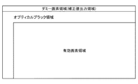
図5は、画素部110の構成例を示している。画素構成として、最も上部にフォトダイオードを持たないダミー画素領域を配置し、順に、遮光されたオプティカルブラック(OB)画素領域、光電変換して得られた信号を出力する有効画素領域を配している。第1の実施形態では、ダミー画素の画素信号を、傾きの比αとオフセット量βを算出するために使用する。ここでは、ダミー画素の画素信号読み出し期間に、定電圧回路400から固定電圧を入力し、列アンプ群130から比較部151に入力される電圧がある固定電圧になるように制御する。なお、第1の実施形態においては、固定電圧として、電圧V1、V2、V3を用いる。
FIG. 5 illustrates a configuration example of the
ダミー画素の読み出し期間におけるAD変換処理について、図6を参照して説明する。まず、図6Aに示すように、固定電圧V1をAD変換する。なお、図3で説明した処理とは異なり、N信号をAD変換するための期間は設ける必要がない。図6Aに示すように、レベル判定期間のランプ回路140から出力されるランプ信号VRAMPを最小値VRAMP(MIN)とすることで、傾きが大きい第二のランプ信号VRAMP(大)で固定電圧V1をAD変換する。AD変換した結果をT1とする。
The AD conversion process in the dummy pixel readout period will be described with reference to FIG. First, as shown in FIG. 6A, the fixed voltage V1 is AD-converted. Unlike the process described with reference to FIG. 3, it is not necessary to provide a period for AD-converting the N signal. As shown in FIG. 6A, by setting the ramp signal VRAMP output from the
続いて、図6Bに示すように、固定電圧V1よりも大きい固定電圧V2をAD変換する。ここで、固定電圧V2は判定レベルVsと同じ電圧とするとよい。図6Bにおいても、レベル判定期間のランプ信号VRAMPを最小値VRAMP(MIN)とすることで、傾きが大きい第二のランプ信号VRAMP(大)で固定電圧V2をAD変換する。AD変換した結果をT2とする。 Subsequently, as shown in FIG. 6B, the fixed voltage V2 larger than the fixed voltage V1 is AD-converted. Here, the fixed voltage V2 may be the same voltage as the determination level Vs. In FIG. 6B as well, by setting the ramp signal VRAMP in the level determination period to the minimum value VRAMP (MIN), the fixed voltage V2 is AD-converted with the second ramp signal VRAMP (large) having a large slope. The result of the AD conversion is defined as T2.
同様に、図6Cに示すように、固定電圧V2よりも大きい固定電圧V3(高レベルのアナログ信号)をAD変換する。図6Cにおいても、レベル判定期間のランプ信号VRAMPを最小値VRAMP(MIN)とすることで、傾きが大きい第二のランプ信号VRAMP(大)で固定電圧V3をAD変換する。AD変換した結果をT3とする。 Similarly, as shown in FIG. 6C, the fixed voltage V3 (high-level analog signal) larger than the fixed voltage V2 is AD-converted. Also in FIG. 6C, by setting the ramp signal VRAMP in the level determination period to the minimum value VRAMP (MIN), the fixed voltage V3 is AD-converted with the second ramp signal VRAMP (large) having a large slope. The result of the AD conversion is defined as T3.
続いて、図6Dに示すように、固定電圧V1をAD変換する。図6Dでは、レベル判定期間のランプ信号VRAMPを最大値VRAMP(MAX)まで上げることで、傾きが小さい第一のランプ信号VRAMP(小)で固定電圧V1のAD変換を行う。AD変換した結果をT4とする。 Subsequently, as shown in FIG. 6D, the fixed voltage V1 is AD-converted. In FIG. 6D, the ramp signal VRAMP in the level determination period is raised to the maximum value VRAMP (MAX), so that the AD conversion of the fixed voltage V1 is performed with the first ramp signal VRAMP (small) having a small slope. The result of the AD conversion is defined as T4.
最後に図6Eに示すように、固定電圧V2をAD変換する。図6Eにおいても、レベル判定期間のランプ信号VRAMPを最大値VRAMP(MAX)まで上げることで、傾きが小さい第一のランプ信号VRAMP(小)で固定電圧V2のAD変換を行う。AD変換した結果をT5とする。 Finally, as shown in FIG. 6E, the fixed voltage V2 is AD-converted. Also in FIG. 6E, by increasing the ramp signal VRAMP during the level determination period to the maximum value VRAMP (MAX), the AD conversion of the fixed voltage V2 is performed with the first ramp signal VRAMP (small) having a small slope. The result of the AD conversion is defined as T5.
これらは、横軸に入力電圧として固定電圧V1、V2、V3、縦軸にAD変換値をとると、図7のように表される。第二のランプ信号VRAMP(大)を用いて固定電圧V1、V2、V3に対するAD変換値を取得し、第一のランプ信号VRAMP(小)を用いて固定電圧V1、V2に対するAD変換値を取得する。 These are represented as shown in FIG. 7 when the horizontal axes represent the fixed voltages V1, V2, and V3 as the input voltages, and the vertical axis represents the AD conversion values. The AD conversion value for the fixed voltages V1, V2, and V3 is obtained using the second ramp signal VRAMP (large), and the AD conversion value for the fixed voltages V1 and V2 is obtained using the first ramp signal VRAMP (small). I do.
上述したようにして求めたT1〜T4の5点の座標から、傾きの比αと、オフセット量βを以下のようにして求める。 From the coordinates of the five points T1 to T4 obtained as described above, the inclination ratio α and the offset amount β are obtained as follows.
まず、傾きの比αは、第二のランプ信号VRAMP(大)の幅の広い2点(図7のP1、P3)と、第一のランプ信号VRAMP(小)の幅の広い2点(図7のP4、P5)との比から計算する。例えば、次の式(2)で求める。 First, the slope ratio α is determined by two points (P1 and P3 in FIG. 7) where the second ramp signal VRAMP (large) is wide and two points where the first ramp signal VRAMP (small) is wide (see FIG. 7). 7 and P4, P5). For example, it is obtained by the following equation (2).

次に、オフセット量βは、判定レベルVsである固定電圧V2を参照電圧として用いる2点(図7のP2、P5)を基準に算出する。例えば、次の式(3)で求められる。 Next, the offset amount β is calculated based on two points (P2 and P5 in FIG. 7) using the fixed voltage V2, which is the determination level Vs, as a reference voltage. For example, it is obtained by the following equation (3).
上記補正値α、βの算出は、撮像素子1の内部で行っても良いし、画像処理部2で行っても良い。
The calculation of the correction values α and β may be performed inside the
式(2)については、傾きの比αを算出する際に、第二のランプ信号VRAMP(大)で変換した固定電圧V1とV3のAD変換値であるT1、T3を用いているため、例えば固定電圧V1とV2などを用いる場合よりも補正精度が良くなる。固定電圧V1とV2を用いて傾きを算出した場合、固定電圧V2のAD変換時にΔVの誤差があった場合、算出した傾きの誤差はΔV/(V2−V1)である。一方、固定電圧V1とV3を用いて傾きを算出した場合、固定電圧V3のAD変換時にΔVの誤差があった場合、算出した傾きの誤差はΔV/(V3−V1)となる。V3はV2よりも大きいため、ΔV/(V2−V1)よりも、ΔV/(V3−V1)の方が小さくなる。ここでいう誤差とは、AD変換時のノイズや、非線形性で生じる誤差である。補正誤差を低減することで、補正後の出力データのレベルのばらつきを抑えることができる。 For the equation (2), when calculating the slope ratio α, T1 and T3, which are the AD conversion values of the fixed voltages V1 and V3 converted by the second ramp signal VRAMP (large), are used. The correction accuracy is higher than when the fixed voltages V1 and V2 are used. When the gradient is calculated using the fixed voltages V1 and V2, and when there is an error of ΔV at the time of AD conversion of the fixed voltage V2, the error of the calculated gradient is ΔV / (V2−V1). On the other hand, when the slope is calculated using the fixed voltages V1 and V3, and when there is an error of ΔV at the time of AD conversion of the fixed voltage V3, the error of the calculated slope is ΔV / (V3−V1). Since V3 is larger than V2, ΔV / (V3-V1) is smaller than ΔV / (V2-V1). The error here is an error generated due to noise at the time of AD conversion or non-linearity. By reducing the correction error, it is possible to suppress variations in the level of the output data after correction.
また、式(3)については、オフセット量βを求める際に、P2、P5の2点を基にしている。そのため、他の点を基に計算した場合よりも、入力電圧が判定レベルVs前後で、第一のランプ信号VRAMP(小)のAD変換値と、第二のランプ信号VRAMP(大)のAD変換値に補正値をかけたものとの差が、小さくなる。つまり、入射光量が変化し、ランプ信号が切り替わった際のAD変換値のずれが小さくなる。 Equation (3) is based on two points P2 and P5 when calculating the offset amount β. Therefore, when the input voltage is around the judgment level Vs, the A / D conversion value of the first ramp signal VRAMP (small) and the A / D conversion of the second ramp signal VRAMP (large) are greater than when the calculation is performed based on other points. The difference from the value multiplied by the correction value becomes smaller. That is, the shift of the AD conversion value when the incident light amount changes and the lamp signal is switched becomes small.
また、本実施形態では、入力した画素信号の信号レベルに応じて異なる傾きを有するランプ信号を切り替えて用いるため、1種類のランプ信号を用いてAD変換した場合よりも、適正なダイナミックレンジを確保できる。例えば、1種類のランプ信号を用いてAD変換した場合、得られた画像全体のAD変換値が想定よりも小さくなり、AD変換後のダイナミックレンジが狭くなってしまう、といったことを防ぐことができる。逆に、画像が明るく、AD変換値が想定よりも大きくなり、AD変換値がダイナミックレンジをオーバーしてしまう、といったことを防ぐことができる。 In the present embodiment, a ramp signal having a different slope is switched and used according to the signal level of the input pixel signal. Therefore, a more appropriate dynamic range is secured than when AD conversion is performed using one type of ramp signal. it can. For example, when AD conversion is performed using one type of ramp signal, it is possible to prevent the AD conversion value of the entire obtained image from becoming smaller than expected and the dynamic range after AD conversion from being narrowed. . Conversely, it is possible to prevent the image from being bright, the AD conversion value being larger than expected, and the AD conversion value exceeding the dynamic range.
上記の通り本第1の実施形態によれば、傾きの異なる複数のランプ信号を切り替えてAD変換する場合に、AD変換値を補正するための補正値の傾きの誤差を低減するとともに、判定レベルVs前後でのAD変換値のずれを小さくすることができる。 As described above, according to the first embodiment, when a plurality of ramp signals having different inclinations are switched and subjected to the AD conversion, the error of the inclination of the correction value for correcting the AD conversion value is reduced, and the determination level is determined. The deviation of the AD conversion value before and after Vs can be reduced.
<第2の実施形態>
次に、本発明の第2の実施形態について説明する。第2の実施形態では、第一の補正値生成方法と、第二の補正値生成方法の2つの補正値生成方法を用いる例について説明する。第一の補正値生成方法は、第1の実施形態において説明した式(2)、式(3)を用いた方法であるので、ここでは説明を省略する。
<Second embodiment>
Next, a second embodiment of the present invention will be described. In the second embodiment, an example using two correction value generation methods, a first correction value generation method and a second correction value generation method, will be described. The first correction value generation method uses the equations (2) and (3) described in the first embodiment, and a description thereof will be omitted.
以下、第二の補正値生成方法について、図7を用いて説明する。まず傾きの比αを、判定レベルVsと同じレベルの固定電圧V2をAD変換して取得した2点(P2、P5)と、固定電圧V2よりも小さい固定電圧V1を用いて取得した2点(P1、P4)を使って求める。例えば、次の式(4)で求める。 Hereinafter, the second correction value generation method will be described with reference to FIG. First, two points (P2, P5) obtained by AD-converting the fixed voltage V2 having the same level as the determination level Vs and two points obtained using the fixed voltage V1 smaller than the fixed voltage V2 ( P1 and P4). For example, it is obtained by the following equation (4).
次に、オフセット量βも、上記傾きの比αと同様の4点(P1、P2、P4、P5)を使って算出する。例えば、次の式(5)で求める。 Next, the offset amount β is also calculated using the same four points (P1, P2, P4, P5) as the inclination ratio α. For example, it is obtained by the following equation (5).
図8は、第2の実施形態における補正値生成方法の切り替え処理のフローチャートを示す。S1では、第一の撮影モードであるか否かを判断する。第一の撮影モードは、列アンプ群130により増幅された画素信号が判定レベルVs以上の場合に第二のランプ信号VRAMP(大)を使用し、画素信号が判定レベルVs未満の場合に第一のランプ信号VRAMP(小)を使用するモードである。第二の撮影モードは、画素信号が判定レベルVs以上の場合に第二のランプ信号VRAMP(大)を使用し、画素信号が判定レベルVs未満の場合に第一のランプ信号VRAMP(小)と第二のランプ信号VRAMP(大)とを切り替えて使用するモードである。
FIG. 8 is a flowchart illustrating a switching process of the correction value generation method according to the second embodiment. In S1, it is determined whether or not the current mode is the first shooting mode. The first shooting mode uses the second ramp signal VRAMP (large) when the pixel signal amplified by the
第一の撮影モードと、第二の撮影モードは、例えば、不図示の表示部に表示されたメニュー画面から、ユーザが選択することにより設定される。なお、本発明はこれらの例に限られるものではなく、任意の条件に応じて、自動的に設定されるようにしても良い。また、第二の撮影モードでは、適切な補正値が算出できた場合(例えば、算出した補正値の信頼性が所定の信頼性よりも高い場合)に、第一のランプ信号VRAMP(小)を用いてAD変換を行う。そして、適切な補正値が算出できない場合(例えば、算出した補正値の信頼性が所定の信頼性以下の場合)に、第二のランプ信号VRAMP(大)を用いてAD変換を行う。 The first shooting mode and the second shooting mode are set, for example, by the user selecting from a menu screen displayed on a display unit (not shown). It should be noted that the present invention is not limited to these examples, and may be set automatically according to arbitrary conditions. In the second shooting mode, when an appropriate correction value can be calculated (for example, when the reliability of the calculated correction value is higher than a predetermined reliability), the first ramp signal VRAMP (small) is output. A / D conversion is performed using the above. Then, when an appropriate correction value cannot be calculated (for example, when the reliability of the calculated correction value is equal to or less than a predetermined reliability), AD conversion is performed using the second ramp signal VRAMP (large).
ここで、適切な補正値が算出できない場合の一例として、列アンプ群130のゲインが変更されてから予め決められた期間が考えられる。ゲインが変更されてからしばらくの間は、同じ入射光量に対する画素信号のAD変換値が、変更前から変化してしまい、適切な補正値を算出することができない。そのような場合に、列アンプ群130の出力信号が判定レベルVs未満の場合にも第二のランプ信号VRAMP(大)を用いてAD変換を行う。この場合、列アンプ群130の出力信号の大きさに関わらず、第二のランプ信号VRAMP(大)を用いてAD変換を行うことになるため、AD変換値を補正する必要が無くなる。
Here, as an example of a case where an appropriate correction value cannot be calculated, a predetermined period after the gain of the
S1で、第一の撮影モードであると判断された場合は、S2に進む。S2では、第一の補正値生成方法を用いて、AD変換時の補正値を生成する。 If it is determined in S1 that the current mode is the first shooting mode, the process proceeds to S2. In S2, a correction value for AD conversion is generated using the first correction value generation method.
一方、S1で第二の撮影モードであると判断された場合は、S3に進む。S3では、第二の補正値生成方法を用いてAD変換時の補正値を生成する。 On the other hand, if it is determined in S1 that the current mode is the second shooting mode, the process proceeds to S3. In S3, a correction value at the time of AD conversion is generated using the second correction value generation method.
例えばS2においては、第一の撮影モードであるため、第一のランプ信号VRAMP(小)と第二のランプ信号VRAMP(大)とを切り替えるのは画素信号が判定レベルVsをまたぐ場合のみである。このとき、第一の補正値生成方法により、判定レベルVs付近でAD変換値が一致するように補正されるため(図9(b))、ランプ信号の切り替え時に生じるレベル差は最小限に抑えられる。またランプ信号の傾きの比を、幅広い入射光量を元に算出しているため、ノイズや非線形性の影響を最小限に抑えられる。 For example, in S2, since the mode is the first shooting mode, switching between the first ramp signal VRAMP (small) and the second ramp signal VRAMP (large) is performed only when the pixel signal crosses the determination level Vs. . At this time, since the A / D conversion value is corrected so as to match near the determination level Vs by the first correction value generation method (FIG. 9B ), the level difference generated when the lamp signal is switched is minimized. Can be Further, since the ratio of the slope of the ramp signal is calculated based on a wide range of incident light amount, the influence of noise and nonlinearity can be minimized.
一方、S3においては、画素信号が判定レベルVs未満の場合は、どの信号レベルであっても、第一のランプ信号VRAMP(小)と第二のランプ信号VRAMP(大)を切り替えられる可能性がある。そのとき、第二の補正値生成方法により、判定レベルVs未満の画素信号に対して、信号レベルが小さい場合と大きい場合の2点で、AD変換値が一致するように補正される(図9(a))。そのため、画素信号が判定レベルVs未満のどこでランプ信号の切替が発生しても、そのときに生じるレベル差を最小限に抑えることができる。 On the other hand, in S3, when the pixel signal is lower than the determination level Vs, there is a possibility that the first ramp signal VRAMP (small) and the second ramp signal VRAMP (large) can be switched at any signal level. is there. At this time, the second correction value generation method corrects the pixel signal having the determination level Vs so that the AD conversion values match at two points when the signal level is low and when the signal level is high (FIG. 9). (a)). Therefore, even if the switching of the ramp signal occurs where the pixel signal is lower than the determination level Vs, the level difference generated at that time can be minimized.
上記の通り第2の実施形態においては、2つの補正値生成方法を状況によって使い分けることで、好適な撮影を実現することが可能となる。 As described above, in the second embodiment, by appropriately using the two correction value generation methods depending on the situation, it is possible to realize a suitable shooting.
なお、上述した第1及び第2の実施形態では、1つの判定レベルVsに応じて、第一のランプ信号VRAMP(小)または第二のランプ信号VRAMP(大)のいずれかを選択するものとして説明した。しかしながら、本発明はこれに限るものではなく、複数の判定レベルを設定して、3種類以上のランプ信号から選択できるようにしてもよい。 In the first and second embodiments described above, one of the first ramp signal VRAMP (small) and the second ramp signal VRAMP (large) is selected according to one determination level Vs. explained. However, the present invention is not limited to this, and a plurality of determination levels may be set so that three or more types of lamp signals can be selected.
以上、本発明をその好適な実施形態に基づいて詳述してきたが、本発明はこれら特定の実施形態に限られるものではなく、この発明の要旨を逸脱しない範囲の様々な形態も本発明に含まれる。上述の実施形態の一部を適宜組み合わせてもよい。 As described above, the present invention has been described in detail based on the preferred embodiments. However, the present invention is not limited to these specific embodiments, and various forms that do not depart from the gist of the present invention are also included in the present invention. included. A part of the above-described embodiments may be appropriately combined.
1:撮像素子、2:画像処理部、140:ランプ回路、150:列アナログデジタル変換器群、151:比較部、152:カウンタ・ラッチ回路、170:信号処理回路、300:コントローラ回路、400:定電圧回路 1: imaging device, 2: image processing unit, 140: lamp circuit, 150: column analog-to-digital converter group, 151: comparison unit, 152: counter / latch circuit, 170: signal processing circuit, 300: controller circuit, 400: Constant voltage circuit
Claims (11)
予め決められた複数の異なる出力レベルのアナログ信号を前記アナログデジタル変換手段に供給する電圧供給手段と、
前記複数の異なる出力レベルのアナログ信号を前記複数の参照信号によりそれぞれ変換して得られた複数のデジタル信号に基づいて、撮像素子の画素部から出力されるアナログ信号を前記アナログデジタル変換手段により変換して得られるデジタル信号を補正するための、前記複数の異なる傾きの比とオフセット量とを算出する算出手段と、を有し、
前記電圧供給手段は、より傾きの大きい参照信号により変換を行う場合に、より傾きの小さい参照信号により変換を行う場合よりも出力レベルが高い少なくとも1つの高レベルのアナログ信号を、前記アナログデジタル変換手段に更に供給し、
前記算出手段は、前記傾きの比を算出するときに、前記高レベルのアナログ信号を変換して得られたデジタル信号を更に用いることを特徴とする信号処理装置。 Analog-to-digital conversion means for converting an analog signal into a digital signal using a plurality of reference signals having different slopes,
Voltage supply means for supplying analog signals of a plurality of predetermined different output levels to the analog-to-digital conversion means,
An analog signal output from a pixel unit of an image sensor is converted by the analog-to-digital conversion unit based on a plurality of digital signals obtained by converting the plurality of analog signals having different output levels using the plurality of reference signals. Calculating means for calculating a ratio and an offset amount of the plurality of different slopes for correcting a digital signal obtained by
The voltage supply means converts at least one high-level analog signal having a higher output level when performing conversion with a reference signal having a larger slope than when converting with a reference signal having a smaller slope. Supply further to the means,
The signal processing apparatus according to claim 1, wherein said calculating means further uses a digital signal obtained by converting said high-level analog signal when calculating said inclination ratio.
前記電圧供給手段は、前記第二の参照信号により変換を行う場合に、前記高レベルのアナログ信号を前記アナログデジタル変換手段に更に供給し、
前記算出手段は、前記第一の参照信号と前記第二の参照信号の前記傾きの比を算出するときに、前記高レベルのアナログ信号を変換して得られたデジタル信号を更に用いることを特徴とする請求項1に記載の信号処理装置。 The plurality of reference signals include a first reference signal and a second reference signal having a greater slope than the first reference signal,
The voltage supply means, when performing the conversion by the second reference signal, further supplies the high-level analog signal to the analog-digital conversion means,
The calculating means may further use a digital signal obtained by converting the high-level analog signal when calculating the ratio of the gradient between the first reference signal and the second reference signal. The signal processing device according to claim 1.
前記撮像素子の画素部から出力されるアナログ信号の信号レベルが予め決められた閾値未満の場合に、前記第一の参照信号を用いて当該アナログ信号の変換を行い、前記信号レベルが前記閾値以上の場合に、前記第二の参照信号を用いて当該アナログ信号の変換を行う第一の撮影モードと、
前記撮像素子の画素部から出力されるアナログ信号の信号レベルが前記閾値未満の場合に、予め決められた条件に基づいて、前記第一の参照信号または前記第二の参照信号のいずれかを用いて当該アナログ信号の変換を行い、前記信号レベルが前記閾値以上の場合に、前記第二の参照信号を用いて当該アナログ信号の変換を行う第二の撮影モードと、
のいずれかにより変換を行うことを特徴とする請求項2に記載の信号処理装置。 The analog-to-digital conversion means,
When the signal level of the analog signal output from the pixel unit of the imaging device is less than a predetermined threshold, the analog signal is converted using the first reference signal, and the signal level is equal to or greater than the threshold. In the case of, the first shooting mode performing the conversion of the analog signal using the second reference signal,
When the signal level of the analog signal output from the pixel unit of the image sensor is less than the threshold, based on a predetermined condition, using either the first reference signal or the second reference signal Performing the conversion of the analog signal, when the signal level is equal to or more than the threshold, a second shooting mode in which the conversion of the analog signal using the second reference signal,
The signal processing device according to claim 2, wherein the conversion is performed by any one of the following.
前記アナログデジタル変換手段は、前記第二の撮影モードにおいて、前記信号レベルが前記予め決められた閾値未満であって、且つ、前記信頼性が前記予め決められた信頼性より高い場合に、前記第一の参照信号を用い、前記信号レベルが前記予め決められた閾値未満であって、且つ、前記信頼性が前記予め決められた信頼性以下の場合に、前記第二の参照信号を用いて変換を行うことを特徴とする請求項4に記載の信号処理装置。 The predetermined condition includes whether the reliability of the ratio of the slope and the offset amount calculated by the calculation unit is higher than a predetermined reliability,
The analog-to-digital conversion means, in the second shooting mode, when the signal level is less than the predetermined threshold, and the reliability is higher than the predetermined reliability, Using one reference signal, if the signal level is less than the predetermined threshold, and if the reliability is less than or equal to the predetermined reliability, converting using the second reference signal The signal processing device according to claim 4, wherein the signal processing is performed.
前記増幅手段のゲインが変更された場合に、前記信頼性が前記予め決められた信頼性よりも高くないと判断することを特徴とする請求項5に記載の信号処理装置。 The analog-to-digital conversion means includes amplification means for applying a gain to the input analog signal,
6. The signal processing device according to claim 5, wherein when the gain of the amplifying unit is changed, the reliability is determined to be not higher than the predetermined reliability.
請求項1乃至9のいずれか1項に記載の信号処理装置と
を有することを特徴とする撮像装置。 The imaging device;
An imaging device comprising: the signal processing device according to claim 1.
前記アナログデジタル変換手段が、前記複数の異なる出力レベルのアナログ信号を、互いに異なる傾きを有する複数の参照信号を用いてデジタル信号に変換するアナログデジタル変換工程と、
算出手段が、前記複数のデジタル信号に基づいて、撮像素子の画素部から出力されるアナログ信号を前記アナログデジタル変換手段により変換して得られるデジタル信号を補正するための、前記複数の異なる傾きの比とオフセット量とを算出する算出工程と、を有し、
前記電圧供給工程では、より傾きの大きい参照信号により変換を行う場合に、より傾きの小さい参照信号により変換を行う場合よりも出力レベルが高い少なくとも1つの高レベルのアナログ信号を、前記アナログデジタル変換手段に供給し、
前記算出工程では、前記傾きの比を算出するときに、前記高レベルのアナログ信号を変換して得られたデジタル信号を用いることを特徴とする信号処理方法。 A voltage supply step of supplying a plurality of predetermined analog signals having different output levels to the analog-to-digital conversion means,
The analog-to-digital conversion means, an analog-to-digital conversion step of converting the plurality of different output level analog signals to digital signals using a plurality of reference signals having mutually different slopes,
Calculating means for correcting, based on the plurality of digital signals, a digital signal obtained by converting an analog signal output from a pixel unit of an image sensor by the analog-to-digital conversion means; A calculating step of calculating the ratio and the offset amount,
In the voltage supply step, when performing conversion using a reference signal having a larger slope, at least one high-level analog signal having a higher output level than when performing conversion using a reference signal having a smaller slope is subjected to the analog-to-digital conversion. Supply to the means,
In the calculating step, a digital signal obtained by converting the high-level analog signal is used when calculating the inclination ratio.
Priority Applications (3)
| Application Number | Priority Date | Filing Date | Title |
|---|---|---|---|
| JP2016040441A JP6643919B2 (en) | 2016-03-02 | 2016-03-02 | Signal processing apparatus and method, and imaging apparatus |
| US15/446,833 US9918033B2 (en) | 2016-03-02 | 2017-03-01 | Signal processing apparatus and signal processing method, and image capturing apparatus |
| CN201710120500.2A CN107154803B (en) | 2016-03-02 | 2017-03-02 | Signal processing apparatus, signal processing method, and image pickup apparatus |
Applications Claiming Priority (1)
| Application Number | Priority Date | Filing Date | Title |
|---|---|---|---|
| JP2016040441A JP6643919B2 (en) | 2016-03-02 | 2016-03-02 | Signal processing apparatus and method, and imaging apparatus |
Publications (3)
| Publication Number | Publication Date |
|---|---|
| JP2017158062A JP2017158062A (en) | 2017-09-07 |
| JP2017158062A5 JP2017158062A5 (en) | 2019-04-11 |
| JP6643919B2 true JP6643919B2 (en) | 2020-02-12 |
Family
ID=59723836
Family Applications (1)
| Application Number | Title | Priority Date | Filing Date |
|---|---|---|---|
| JP2016040441A Active JP6643919B2 (en) | 2016-03-02 | 2016-03-02 | Signal processing apparatus and method, and imaging apparatus |
Country Status (3)
| Country | Link |
|---|---|
| US (1) | US9918033B2 (en) |
| JP (1) | JP6643919B2 (en) |
| CN (1) | CN107154803B (en) |
Families Citing this family (5)
| Publication number | Priority date | Publication date | Assignee | Title |
|---|---|---|---|---|
| JP6556001B2 (en) * | 2015-09-24 | 2019-08-07 | キヤノン株式会社 | Image reading device |
| KR20190044261A (en) * | 2017-10-20 | 2019-04-30 | 에스케이하이닉스 주식회사 | Single-slope comparator with low-noise, and analog to digital converting apparatus and cmos image sensor thereof |
| CN109714057B (en) * | 2018-12-26 | 2020-04-07 | 北京华大九天软件有限公司 | Dynamic digital-to-analog signal conversion model and modeling method |
| CN114143481A (en) * | 2020-09-04 | 2022-03-04 | 格科微电子(上海)有限公司 | Method for optimizing performance of image sensor based on self-adaptive programmable analog-to-digital conversion |
| CN114910152B (en) * | 2022-05-30 | 2024-03-12 | 江西众加利高科技股份有限公司 | Precision correction method for weighing metering instrument |
Family Cites Families (18)
| Publication number | Priority date | Publication date | Assignee | Title |
|---|---|---|---|---|
| JP4682750B2 (en) * | 2005-08-22 | 2011-05-11 | ソニー株式会社 | DA converter |
| JP4882652B2 (en) * | 2006-10-06 | 2012-02-22 | ソニー株式会社 | Solid-state imaging device, driving method of solid-state imaging device, and imaging device |
| GB0902822D0 (en) * | 2009-02-19 | 2009-04-08 | Cmosis Nv | Analog-to-digital conversation in pixel arrays |
| JP2010251957A (en) * | 2009-04-14 | 2010-11-04 | Sony Corp | A/d converter, solid-state image sensing device, and camera system |
| KR101566003B1 (en) * | 2009-04-20 | 2015-11-16 | 삼성전자주식회사 | - - Analog-digital converting method Analog-digital converter and Image sensor having the same |
| JP5531797B2 (en) * | 2010-06-15 | 2014-06-25 | ソニー株式会社 | Solid-state imaging device and camera system |
| US8519875B2 (en) * | 2011-04-12 | 2013-08-27 | Maxim Integrated Products, Inc. | System and method for background calibration of time interleaved analog to digital converters |
| US8730081B2 (en) * | 2012-03-19 | 2014-05-20 | Omnivision Technologies, Inc. | Calibration in multiple slope column parallel analog-to-digital conversion for image sensors |
| JP5865272B2 (en) * | 2012-03-30 | 2016-02-17 | キヤノン株式会社 | Photoelectric conversion device and imaging system |
| JP5847737B2 (en) * | 2012-03-30 | 2016-01-27 | キヤノン株式会社 | Photoelectric conversion device and imaging system |
| JP5893550B2 (en) | 2012-04-12 | 2016-03-23 | キヤノン株式会社 | Imaging apparatus and imaging system |
| WO2013179615A1 (en) * | 2012-05-29 | 2013-12-05 | パナソニック株式会社 | Ramp generator circuit and solid-state imaging device |
| US8854244B2 (en) * | 2012-09-19 | 2014-10-07 | Aptina Imaging Corporation | Imagers with improved analog-to-digital converters |
| KR20140067408A (en) * | 2012-11-26 | 2014-06-05 | 삼성전자주식회사 | Solid state pick-up device and control method therefore |
| GB201300999D0 (en) * | 2013-01-21 | 2013-03-06 | Cmosis Nv | Analog-to-digital conversation in pixel arrays |
| JP6478467B2 (en) * | 2013-03-28 | 2019-03-06 | キヤノン株式会社 | Imaging device, driving method of imaging device, and imaging system |
| JP2015162751A (en) * | 2014-02-26 | 2015-09-07 | キヤノン株式会社 | Photoelectric conversion device and imaging system |
| KR102195409B1 (en) * | 2014-05-29 | 2020-12-30 | 삼성전자주식회사 | Device and method for lamp signal calibration and image sensor using the same |
-
2016
- 2016-03-02 JP JP2016040441A patent/JP6643919B2/en active Active
-
2017
- 2017-03-01 US US15/446,833 patent/US9918033B2/en active Active
- 2017-03-02 CN CN201710120500.2A patent/CN107154803B/en active Active
Also Published As
| Publication number | Publication date |
|---|---|
| CN107154803A (en) | 2017-09-12 |
| JP2017158062A (en) | 2017-09-07 |
| US20170257592A1 (en) | 2017-09-07 |
| US9918033B2 (en) | 2018-03-13 |
| CN107154803B (en) | 2020-12-22 |
Similar Documents
| Publication | Publication Date | Title |
|---|---|---|
| US9736406B2 (en) | Image capturing apparatus and control method thereof | |
| JP6643919B2 (en) | Signal processing apparatus and method, and imaging apparatus | |
| JP5034610B2 (en) | Solid-state imaging device, signal processing method for solid-state imaging device, and imaging device | |
| TWI404411B (en) | Solid-state imaging device, control method therefor, and camera system | |
| US9848150B2 (en) | Image pickup apparatus comprising A/D converter with offset and gain correction based on amplitude of input signal | |
| US10027919B2 (en) | Signal processing apparatus, image capturing apparatus, control apparatus, signal processing method, and control method | |
| JP6164867B2 (en) | Solid-state imaging device, control method thereof, and control program | |
| US20160212365A1 (en) | Signal processing device and method, imaging device, and imaging apparatus | |
| US7876371B2 (en) | Systems and methods to perform digital correlated double sampling using successive approximation analog to digital conversion techniques | |
| JP6494301B2 (en) | Imaging apparatus and control method thereof | |
| US10313617B2 (en) | Image capturing apparatus, control method for the same, and storage medium | |
| JP6808564B2 (en) | Signal processing devices and methods, image sensors, and image pickup devices | |
| JP6525602B2 (en) | Image pickup apparatus and control method thereof | |
| JP6223267B2 (en) | Solid-state imaging device and imaging apparatus | |
| JP6433276B2 (en) | Imaging apparatus, control method therefor, program, and storage medium | |
| JP2018050234A (en) | Imaging apparatus and method of processing imaging apparatus | |
| US11284017B2 (en) | Image pickup device and storage medium | |
| JP5588729B2 (en) | Image signal processing device | |
| JP2017152838A (en) | Imaging apparatus and control method for imaging apparatus | |
| JP2021153291A (en) | Imaging apparatus, computer program, and storage medium | |
| JP2017152853A (en) | Imaging apparatus and control method for imaging apparatus | |
| JP6824687B2 (en) | Solid-state image sensor, image sensor, control method of solid-state image sensor, program, and storage medium | |
| JP2020036256A (en) | Imaging device and control method thereof |
Legal Events
| Date | Code | Title | Description |
|---|---|---|---|
| A521 | Request for written amendment filed |
Free format text: JAPANESE INTERMEDIATE CODE: A523 Effective date: 20190301 |
|
| A621 | Written request for application examination |
Free format text: JAPANESE INTERMEDIATE CODE: A621 Effective date: 20190301 |
|
| A977 | Report on retrieval |
Free format text: JAPANESE INTERMEDIATE CODE: A971007 Effective date: 20191127 |
|
| TRDD | Decision of grant or rejection written | ||
| A01 | Written decision to grant a patent or to grant a registration (utility model) |
Free format text: JAPANESE INTERMEDIATE CODE: A01 Effective date: 20191209 |
|
| A61 | First payment of annual fees (during grant procedure) |
Free format text: JAPANESE INTERMEDIATE CODE: A61 Effective date: 20200107 |
|
| R151 | Written notification of patent or utility model registration |
Ref document number: 6643919 Country of ref document: JP Free format text: JAPANESE INTERMEDIATE CODE: R151 |