JP6525602B2 - Image pickup apparatus and control method thereof - Google Patents
Image pickup apparatus and control method thereof Download PDFInfo
- Publication number
- JP6525602B2 JP6525602B2 JP2015010676A JP2015010676A JP6525602B2 JP 6525602 B2 JP6525602 B2 JP 6525602B2 JP 2015010676 A JP2015010676 A JP 2015010676A JP 2015010676 A JP2015010676 A JP 2015010676A JP 6525602 B2 JP6525602 B2 JP 6525602B2
- Authority
- JP
- Japan
- Prior art keywords
- value
- correction value
- signal
- analog
- offset correction
- Prior art date
- Legal status (The legal status is an assumption and is not a legal conclusion. Google has not performed a legal analysis and makes no representation as to the accuracy of the status listed.)
- Active
Links
- 238000000034 method Methods 0.000 title claims description 98
- 238000012937 correction Methods 0.000 claims description 192
- 125000004122 cyclic group Chemical group 0.000 claims description 118
- 238000003384 imaging method Methods 0.000 claims description 68
- 238000001914 filtration Methods 0.000 claims description 65
- 230000008859 change Effects 0.000 claims description 63
- 238000012545 processing Methods 0.000 claims description 52
- 230000008569 process Effects 0.000 claims description 51
- 238000006243 chemical reaction Methods 0.000 claims description 49
- 238000004364 calculation method Methods 0.000 claims description 8
- 238000001514 detection method Methods 0.000 claims description 6
- 230000003321 amplification Effects 0.000 claims description 4
- 238000003199 nucleic acid amplification method Methods 0.000 claims description 4
- 235000019557 luminance Nutrition 0.000 description 12
- 238000010586 diagram Methods 0.000 description 10
- 230000006641 stabilisation Effects 0.000 description 6
- 238000011105 stabilization Methods 0.000 description 6
- ATCJTYORYKLVIA-SRXJVYAUSA-N vamp regimen Chemical compound O=C1C=C[C@]2(C)[C@H]3[C@@H](O)C[C@](C)([C@@](CC4)(O)C(=O)CO)[C@@H]4[C@@H]3CCC2=C1.C=1N=C2N=C(N)N=C(N)C2=NC=1CN(C)C1=CC=C(C(=O)N[C@@H](CCC(O)=O)C(O)=O)C=C1.O([C@H]1C[C@@](O)(CC=2C(O)=C3C(=O)C=4C=CC=C(C=4C(=O)C3=C(O)C=21)OC)C(=O)CO)[C@H]1C[C@H](N)[C@H](O)[C@H](C)O1.C([C@H](C[C@]1(C(=O)OC)C=2C(=CC3=C(C45[C@H]([C@@]([C@H](OC(C)=O)[C@]6(CC)C=CCN([C@H]56)CC4)(O)C(=O)OC)N3C=O)C=2)OC)C[C@@](C2)(O)CC)N2CCC2=C1NC1=CC=CC=C21 ATCJTYORYKLVIA-SRXJVYAUSA-N 0.000 description 6
- 230000000694 effects Effects 0.000 description 5
- 230000006872 improvement Effects 0.000 description 4
- 230000010354 integration Effects 0.000 description 4
- 230000009467 reduction Effects 0.000 description 4
- 238000012546 transfer Methods 0.000 description 4
- 230000004913 activation Effects 0.000 description 3
- 238000004891 communication Methods 0.000 description 3
- 238000005457 optimization Methods 0.000 description 3
- 230000007704 transition Effects 0.000 description 3
- 238000001816 cooling Methods 0.000 description 2
- 230000007423 decrease Effects 0.000 description 2
- 230000006866 deterioration Effects 0.000 description 2
- 230000000737 periodic effect Effects 0.000 description 2
- 230000000007 visual effect Effects 0.000 description 2
- 239000003086 colorant Substances 0.000 description 1
- 230000003247 decreasing effect Effects 0.000 description 1
- 230000001934 delay Effects 0.000 description 1
- 230000003111 delayed effect Effects 0.000 description 1
- 238000011161 development Methods 0.000 description 1
- 238000005516 engineering process Methods 0.000 description 1
- 238000005286 illumination Methods 0.000 description 1
- 230000005389 magnetism Effects 0.000 description 1
- 230000003287 optical effect Effects 0.000 description 1
- 238000003672 processing method Methods 0.000 description 1
- 230000035945 sensitivity Effects 0.000 description 1
- 230000003595 spectral effect Effects 0.000 description 1
Images


Landscapes
- Transforming Light Signals Into Electric Signals (AREA)
- Studio Devices (AREA)
Description
本発明は、撮像装置及びその制御方法に関し、特に、撮像素子から読み出したアナログ信号をデジタル信号に変換する撮像装置及びその制御方法に関する。 The present invention relates to an imaging apparatus and its control method, and more particularly to an imaging apparatus that converts an analog signal read out from an imaging device into a digital signal and its control method.
従来、テレビジョンの規格として、水平1920画素、垂直1080画素のフルハイビジョンと呼ばれる規格が一般的によく用いられていた。しかし近年では、水平3840画素、垂直2160画素の4K2Kと呼ばれるテレビジョン規格への移行が進んできている。さらに今後、水平7680画素、垂直4320画素の8K4K(スーパーハイビジョン)と呼ばれる、次世代テレビジョン規格への移行が予定されている。また、多画素化と共に、フレームレートにおいても高速化の一途を辿っている。 Conventionally, a standard called full high-definition television with 1920 horizontal pixels and 1080 vertical pixels has been commonly used as a television standard. However, in recent years, the transition to a television standard called 4K2K called horizontal 3840 pixels and vertical 2160 pixels has been advanced. In the future, a transition to the next-generation television standard, called 8K4K (Super Hi-Vision) with 7680 pixels horizontally and 4320 pixels vertically, is planned. In addition to the increase in the number of pixels, the frame rate has also been steadily increased.
このようなテレビジョン規格の移行に伴い、テレビジョン映像を撮影する撮像装置に対して多画素化・高フレームレート化が要求されており、これを満足するために、撮像素子が映像を読み出す速度を高速化していくことが一つの課題となっている。読み出し速度を高速化するためには、撮像素子が有するAD変換器の処理速度を高速化することが必要不可欠であり、AD変換器の高速化に関する様々な技術が提案されている。 With the transition of such television standards, an increase in the number of pixels and a increase in frame rate are required for imaging devices that capture television images, and in order to satisfy this, the speed at which the imaging device reads the images One of the issues is to speed up In order to speed up the reading speed, it is essential to speed up the processing speed of the AD converter that the imaging device has, and various techniques for speeding up the AD converter have been proposed.
また、読み出し速度の高速化に加え、S/N比の改善とダイナミックレンジの拡大を目的とした、階調精度の向上に対する要求も高い。そのため、回路規模が増大したり、処理時間が延びるようなこと無く階調精度を向上させることが、今後の画像性能を向上させる上で、重要な課題となっている。 Further, in addition to the speeding up of the reading speed, there is also a high demand for the improvement of the gradation accuracy for the purpose of the improvement of the S / N ratio and the expansion of the dynamic range. Therefore, to improve the gradation accuracy without increasing the circuit scale or extending the processing time has become an important issue in order to improve the image performance in the future.
このような課題に対し、特許文献1では、次のような構成を有する撮像装置を開示している。すなわち、撮像素子内にある列アンプ回路を用いて、画素信号を第1のゲインで増幅した第1の画素信号と、第1のゲインより大きい第2のゲインで増幅した第2の画素信号とを、それぞれ異なるADコンバータ回路を用いてアナログデジタル(AD)変換する。そして、画素信号のレベルに応じて、AD変換後の第1の画素信号と第2の画素信号のうち、いずれか一方を選択的に出力させる。このような構成にすることで、ダイナミックレンジの拡大と、S/N比の改善を実現することが可能となる。
With respect to such a problem,
更に、特許文献1では、選択的に読み出した第1の画素信号と第2の画素信号を同じゲインレベルにレベルシフトした後に、ゲイン誤差もしくはオフセット誤差を検出し、この検出値に基づいて画素信号を補正する技術についても提案している。このような処理を行うことで、選択的に読み出した第1の画素信号と第2の画素信号とから1枚の画像を合成した際に生じる、信号レベルの段差を低減させることができる。
Furthermore, according to
しかしながら、特許文献1では、検出値を用いて算出された補正値のばらつき(変動)については考慮されていない。補正値が変動する主な要因としては、急激な温度変化、撮像素子の駆動方法の切替え、列アンプに供給している電源のノイズ、配線ノイズ、外乱ノイズ(例えば、モーター駆動等で発生する磁気ノイズの飛び込み)などがある。このような要因により補正値が変動した状態で、特許文献1に開示されているように第1の画素信号及び第2の画素信号とから1枚の画像を合成した場合、信号レベルの段差が見えてしまう。
However, in
例えば、フレーム毎に補正値を算出し、更新していくような補正方法を用いた場合、信号レベルの段差が発生するフレームと、信号レベルの段差が発生しないフレームが存在すると、見た目上違和感のある映像となってしまう。 For example, in the case of using a correction method in which a correction value is calculated and updated for each frame, there is a frame in which a level difference in signal level occurs and a frame in which a level difference in signal level does not occur. It becomes a certain picture.
また、1フレーム分の画像を分割した領域毎に別々の補正値を算出し、補正する方法を用いた場合、領域毎に段差が発生する領域と発生しない領域が存在するため、見た目上違和感のある画像となってしまう。特に、被写体のコントラストが低く、徐々に輝度レベルが変化するような映像では、顕著に目立つ。 In addition, when using a method of calculating and correcting different correction values for each area obtained by dividing an image for one frame, there is an area in which a step is generated and an area in which no level difference is generated for each area. It becomes an image. In particular, in an image in which the contrast of the subject is low and the luminance level changes gradually, the image is noticeable.
本発明は上記問題点を鑑みてなされたものであり、フレーム間、もしくは画面内の領域間で、信号レベルの段差が発生したり、段差のレベルが変化するような不自然な映像となることを防ぐことを目的とする。 The present invention has been made in view of the above problems, and it is an unnatural image in which a level difference of signal level occurs or a level difference of level changes between frames or in an area in a screen. The purpose is to prevent
上記目的を達成するために、本発明の撮像装置は、複数の画素が2次元に配置された画素部と、互いに異なる傾きを有する複数の参照信号を用いてアナログ信号をデジタル信号に変換するアナログデジタル変換手段と、予め決められた複数の異なる出力レベルのアナログ信号を前記アナログデジタル変換手段に供給する電圧供給手段と、前記電圧供給手段により供給される前記複数の異なる出力レベルのアナログ信号を前記アナログデジタル変換手段により前記複数の参照信号を用いてそれぞれ変換して得られた複数のデジタル信号に基づいて、前記複数の参照信号を用いて前記画素部から出力されるアナログ信号を前記アナログデジタル変換手段により変換して得られるデジタル信号の傾き及びオフセットを補正するための補正値を算出する算出手段と、を有し、前記算出手段は、前記オフセットを補正するためのオフセット補正値を巡回係数により重み付け加算するフィルタリング処理を行い、新たに取得したフィルタリング処理前のオフセット補正値と、前のフレームにおけるフィルタリング処理後のオフセット補正値との差分が閾値よりも大きい場合に、前記巡回係数を0に設定する。 In order to achieve the above object, an imaging device according to the present invention is an analog that converts an analog signal into a digital signal using a pixel unit in which a plurality of pixels are two-dimensionally arranged and a plurality of reference signals having different inclinations. digital conversion means, and voltage supply means for supplying a plurality of different output level analog signals of a previously determined in the analog-digital conversion means, the analog signals of the plurality of different power levels supplied by the voltage supply means the The analog-to-digital conversion of an analog signal output from the pixel unit using the plurality of reference signals based on a plurality of digital signals obtained by converting each of the plurality of reference signals by the analog-to-digital conversion means to calculate the correction value for correcting the slope and offset of the digital signal obtained by converting by means A calculation means, wherein the calculating means performs a filtering process of weighted addition by cyclic coefficient offset correction value for correcting the offset, before newly acquired filtering and offset correction value, before When the difference between the frame and the offset correction value after the filtering process is larger than a threshold, the cyclic coefficient is set to zero .
本発明によれば、フレーム間、もしくは画面内の領域間で、信号レベルの段差が発生したり、段差のレベルが変化するような不自然な映像となることを防ぐことができる。 According to the present invention, it is possible to prevent an unnatural image in which a level difference in signal level occurs or a level level changes between frames or in an area in a screen.
以下、添付図面を参照して本発明を実施するための形態を詳細に説明する。 Hereinafter, embodiments of the present invention will be described in detail with reference to the attached drawings.
<第1の実施形態>
図1は、本発明の第1の実施形態における撮像装置で用いられる撮像素子1の構成を示すブロック図であり、撮像素子1と、撮像素子1により得られた画像データの出力先である画像処理部2とを示している。第1の実施形態における撮像素子1は、並列型AD変換器を実装したCMOSイメージセンサである。画像処理部2は、撮像素子1が出力する画像データに対し、ホワイトバランス処理や、ガンマ処理などの現像処理を行い、最終的に記録媒体に記録する。また、画像処理部2はCPUを内蔵しており、このCPUにより、撮像装置の動作モードに応じて撮像素子1と通信(例えばシリアル通信)し、制御を行う。
First Embodiment
FIG. 1 is a block diagram showing a configuration of an
撮像素子1において、タイミング制御部100は撮像素子1の各ブロックに対して動作クロック信号及びタイミング信号を供給し、動作を制御する。
In the
画素部110は、2次元に配置された複数の画素を含み、各画素の光電変換素子において入射光量に応じて光電変換して得られた電荷を、電圧に変換して出力する。各々の画素には、カラーフィルタとマイクロレンズが実装されている。なお、カラーフィルタとして、R(赤)、G(緑)、B(青)の3色の、いわゆるRGB原色カラーフィルタによるベイヤー配列の周期構造をとっているのが一般的であるが、必ずしもこの限りではない。
The
垂直走査回路120は、画素部110の各画素により得られた画素信号を1フレーム期間内に順次読み出すためのタイミング制御を行う。一般的に読み出しは、1フレーム中の上部の行から下部の行にかけて、行単位で順次行われる。
The
列アンプ群130は、各列にそれぞれ設けられた複数の列アンプから成り、画素部110から読みだされた画素信号を電気的に増幅するために用いられる。列アンプ群130で画素信号を増幅することにより、後段のランプ回路140や列アナログデジタル変換器群(列ADC群)150が出すノイズとのS/N比を改善させる。ただし、画素部110の出すノイズに対し、ランプ回路140や列ADC群150が出すノイズが十分小さい回路構造においては、列アンプ群130は必ずしも必須ではない。
The
定電圧回路400は、画素部110と列アンプ群130とを繋ぐ信号線に、固定の電圧を供給する電圧供給手段として動作する。なお、第1の実施形態では定電圧回路400を用いるが、ある一定の電圧で信号をクリップするようなクリップ回路などに応用できる回路を用いても良い。
The
ランプ回路140は、時間方向に一定のスロープ(傾き)を持つランプ形状の電圧信号(ランプ信号)を発生する信号発生器である。列ADC群150は、列毎に比較部151とカウンタ・ラッチ回路152とからなる列ADCを有する。比較部151は、列アンプ群130により増幅された画素信号(アナログ信号)と、ランプ回路140からのランプ信号とを比較して、信号の大小関係を示す信号を出力する。そしてカウンタ・ラッチ回路152が、比較部151からの信号に応じてカウンタ値をラッチすることで、アナログ−デジタル変換が行われる。なお、比較部151とカウンタ・ラッチ回路152の詳細な動作は後述する。カウンタ・ラッチ回路152に保持された1行分のデジタル画像データは、水平転送回路160により端の行から順に読みだされる。
The
水平転送回路160により読み出された画像データは信号処理回路170に入力される。信号処理回路170はデジタル的に信号処理を行う回路であり、デジタル処理で一定量のオフセット値を加える他に、シフト演算や乗算を行うことで、簡易にゲイン演算を行うことができる。また、画素部110に、遮光した画素領域(OB画素部)を形成し、OB画素部の画素から得られる信号を利用したデジタルの黒レベルクランプ動作を行っても良い。更に、入力された画像データに基づいて、後述するように、ランプ回路140から出力されるランプ信号を、タイミング制御部100を介して制御する。
The image data read by the
信号処理回路170により処理された画像データは、外部出力回路180に渡される。外部出力回路180は、シリアライザー機能を有し、信号処理回路170からの多ビットの入力パラレル信号をシリアル信号に変換する。また、このシリアル信号を、例えばLVDS信号等に変換し、画像処理部2に出力する。
The image data processed by the
コントローラ回路300は、画像処理部2とのI/F部であり、シリアル通信回路などを用いて、画像処理部2のCPUから撮像素子1への制御を受ける。
The
次に、撮像素子1の列ADC群150を用いた基本的なAD変換の原理について、図2を用いて説明する。列ADC群150は、上述したように、列毎に比較部151とカウンタ・ラッチ回路152を有している。また、図2(a)に示すように、比較部151は、列アンプ群130から出力される画素信号VAMPと、ランプ回路140から出力されるランプ信号VRAMPとを比較し、その結果を出力する。
Next, the principle of basic AD conversion using the
図2(b)に示すように、画素部110からの画素信号VAMPの読み出し開始に先立って比較部151の動作を開始する(時刻t1)。列アンプ群130の各列アンプの動作が安定すると、時刻t2において、カウンタ・ラッチ回路152のカウント値をリセットする。このカウンタ・ラッチ回路152のカウントリセットタイミングと同期して、ランプ回路140から出力されるランプ信号VRAMPの信号レベルは、時刻t2から時間の経過とともに増加する。比較部151の出力は、列アンプ群130から出力される画素信号VAMPの信号レベルをランプ回路140から出力されるランプ信号VRAMPの信号レベルが超えた時に反転する(時刻t3)。カウンタ・ラッチ回路152は、カウント値をリセットしてから、比較部151の出力が反転するまでの期間(時刻t2〜時刻t3)、カウント動作を行う。この動作により、列アンプ群130により増幅された画素信号の出力レベルに比例したカウント値が得られるため、こうして得られたカウント値がAD変換結果となる。なお、ここで説明した画素信号とランプ信号の比較方法、カウンタ・ラッチ回路によるカウント方法などはあくまで一例であり、カウント値をリセットしてから比較部151の出力が反転するまでの期間を検出できれば、他の方法で実施してもかまわない。
As shown in FIG. 2B, the operation of the
図3は、第1の実施形態におけるランプ回路140及び列ADC群150の動作を説明する図である。図3において、横軸は時間、グラフ上部の縦軸は出力レベル、グラフ下部は、比較部151の出力を示している。図3を参照して、列アンプ群130の出力信号VAMPの信号レベルに応じて、ランプ回路140から出力されるランプ信号VRAMPのスロープを変える例について説明する。
FIG. 3 is a diagram for explaining the operation of the
一般的に、単位画素からの信号の読み出し処理においては、まずN信号(ノイズレベル)の読み出し及びAD変換を行い、その後にS信号(ノイズレベル+信号レベル)の読み出し及びAD変換を行う。そして、信号処理回路170で変換されたS信号とN信号との差分をとることでノイズ成分を打ち消すことで、S/Nの良い信号を得る。
Generally, in the process of reading out a signal from a unit pixel, reading out and AD conversion of an N signal (noise level) is first performed, and thereafter reading out and AD conversion of an S signal (noise level + signal level). Then, the difference between the S signal and the N signal converted by the
まず、N信号のAD変換を行うために、時刻t11で比較部151の動作を開始し、時刻t12でカウンタ・ラッチ回路152のカウントをリセットすると共に、ランプ回路140から出力されるランプ信号VRAMPの信号レベルを変化させる。ここで、ノイズレベルであるN信号の信号レベルは小さいため、N信号のAD変換には、傾きが小さい第一のランプ信号VRAMP(小)(第一の参照信号)を用いる。そして、カウンタ・ラッチ回路152のカウントをリセットしてから、比較部151の出力が反転するまでの期間(時刻t12〜時刻t13)、カウント動作を行うことで、N信号をAD変換する。
First, in order to perform AD conversion of the N signal, the operation of the
次に、画素部110に蓄積された電荷に応じた信号を読み出して列アンプ群130により増幅された出力信号であるS信号に対し、レベル判定期間に、ランプ回路140はある一定の判定レベルVsを最大レベルとする判定用ランプ信号を比較部151に出力する。そして、S信号との比較を行う。ここでは、時刻t14においてカウンタ・ラッチ回路152のカウント値をリセットすると共に、ランプ回路140は所定の判定レベルVsを最大レベルに持つ判定用ランプ信号の出力を開始する。S信号の信号レベルが判定レベルVs以上であれば(S≧Vs)、比較部151の出力は反転しないため、時刻t16でレベル判定期間が終了するまでカウント値が増え続ける。これに対し、S信号の信号レベルが判定レベルVsより小さければ(S<Vs)、例えば時刻t15で比較部151の出力が反転するため、カウント値の増加が終了する。このように、カウンタ・ラッチ回路152のカウント値により、信号処理回路170では、S信号の信号レベルが判定レベルVsよりも大きいか小さいかを判断することができる。なお、カウンタ・ラッチ回路152のカウント値をリセットするタイミングを、ランプ回路140の出力が判定レベルVsに安定した時点とし、S信号の信号レベルが判定レベルVsより小さい(S<Vs)場合に、カウント値が0となるように制御してもよい。
Next, the signal corresponding to the charge stored in the
S信号の信号レベルが判定レベルVsよりも小さい場合は、時刻t17から、N信号と同じ第一のランプ信号VRAMP(小)を用いてS信号のAD変換を行う。これにより、図3に示す例では、時刻t17から時刻t18の間のカウント値が得られる。一方、S信号の信号レベルが判定レベルVs以上である場合は、第一のランプ信号VRAMP(小)よりもスロープがα倍の第二のランプ信号VRAMP(大)(第二の参照信号)を用いて、S信号のAD変換を行う。これにより、図3に示す例では、時刻t17から時刻t19の間のカウント値が得られる。 If the signal level of the S signal is smaller than the determination level Vs, AD conversion of the S signal is performed from time t17 using the same first ramp signal VRAMP (small) as the N signal. Thereby, in the example shown in FIG. 3, the count value between time t17 and time t18 is obtained. On the other hand, when the signal level of the S signal is equal to or higher than the determination level Vs, the second ramp signal VRAMP (large) (second reference signal) whose slope is α times that of the first ramp signal VRAMP (small) is selected. The AD conversion of the S signal is performed using this. Thereby, in the example shown in FIG. 3, the count value between time t17 and time t19 is obtained.
図4は、出力レベルに応じて傾きの異なるランプ信号を用いる場合の、出力信号の信号レベルとAD変換結果との関係を示す図である。図4の横軸は列アンプ群130の出力信号レベルを示し、縦軸はS信号のAD変換後のデジタル値を示している。実線は、比較部151及びカウンタ・ラッチ回路152でAD変換され、水平転送回路160を経て、信号処理回路170に入力されるデジタル値(AD変換値)を表している。上述したように、判定レベルVsより信号レベルが小さいS信号は第一のランプ信号VRAMP(小)を用いて、また、判定レベルVs以上の信号レベルを持つS信号は第二のランプ信号VRAMP(大)を用いてAD変換される。そのため、図4(a)に示すように、判定レベルVsの前後で、AD変換後のS信号の整合が取れていないことになる。
FIG. 4 is a diagram showing the relationship between the signal level of the output signal and the AD conversion result when using ramp signals having different slopes according to the output level. The horizontal axis of FIG. 4 indicates the output signal level of the
そのため、判定レベルVsよりも信号レベルが大きいS信号のAD変換値に対しては、まず、信号処理回路170にて、第一のランプ信号VRAMP(小)と第二のランプ信号VRAMP(大)の傾きの比αを乗算する。更に、判定レベルVsで段差が無くなるようにオフセット量βを加算することで、入射光量に応じた画素信号の信号レベルとAD変換値が一次的な関係になるように補正を行う。
Therefore, with respect to the AD conversion value of the S signal whose signal level is larger than the determination level Vs, the
上述した補正を行わない状態で、有効画素の映像を出力すると、ある輝度で段差が残ったような違和感のある映像となってしまう。この補正に用いる補正値は、撮像素子の温度、撮像素子の駆動タイミング(列アンプ群130のゲインや動作状態等)、駆動設定(電源設定等)によって理想的な補正目標値が変わるため、これらの条件に変化が起きた際には、補正値の再取得が必要である。 If the image of the effective pixel is output without performing the above-described correction, the image will have an uncomfortable feeling as if a step remains at a certain luminance. The correction value used for this correction changes the ideal correction target value depending on the temperature of the image sensor, the drive timing of the image sensor (such as the gain and operating state of the column amplifier group 130), and the drive setting (such as power setting). When a change occurs in the condition of (1), it is necessary to reacquire the correction value.
また、電源起動時、及び撮像素子1の駆動方法の切替え直後に生じる補正値の急激な変化や、列アンプ群130に供給している電源のノイズ、配線ノイズ、外乱ノイズによって生じる、一時的な補正値の変動を、可能な限り低減させる必要がある。外乱ノイズは、例えば、モーター駆動等で発生する磁気ノイズの飛び込み等を含む。なお、補正値の変動の低減方法の詳細については、後述する。
In addition, a temporary change caused by a sudden change of the correction value occurring at the time of power activation and immediately after the switching of the driving method of the
次に、第一のランプ信号VRAMP(小)と第二のランプ信号VRAMP(大)の傾きの比αと、オフセット量βを算出する処理の一例について説明する。 Next, an example of processing for calculating the ratio α of the slopes of the first ramp signal VRAMP (small) and the second ramp signal VRAMP (large) and the offset amount β will be described.
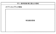
図5は、画素部110の構成例を示している。画素構成として、最も上部にフォトダイオードを持たないダミー画素領域を配置し、順に、遮光されたオプティカルブラック(OB)画素領域、光電変換して得られた信号を出力する有効画素領域を配している。第1の実施形態では、ダミー画素を傾きの比αとオフセット量βを算出するために使用する。ここでは、ダミー画素の画素信号読み出し期間に、定電圧回路400から固定電圧を入力し、列アンプ群130から比較部151に入力される電圧がある固定電圧になるように制御する。なお、第1の実施形態においては、固定電圧として、判定レベルVsより小さい電圧V1及びV2を用いる。
FIG. 5 shows a configuration example of the
ダミー画素の読み出し期間におけるAD変換処理について、図6を参照して説明する。図6Aでは、固定電圧V1をAD変換する。なお、図3で説明した処理とは異なり、N信号をAD変換するための期間は設ける必要がない。図6Aに示すように、レベル判定期間のランプ回路140から出力されるランプ信号VRAMPを最大値VRAMP(MAX)まで上げることで、傾きが小さい第一のランプ信号VAMP(小)で固定電圧V1のAD変換を行う。AD変換した結果をV1Lとする。
The AD conversion process in the reading period of the dummy pixel will be described with reference to FIG. In FIG. 6A, the fixed voltage V1 is AD converted. Unlike the process described with reference to FIG. 3, there is no need to provide a period for AD converting the N signal. As shown in FIG. 6A, by raising the ramp signal VRAMP output from the
続いて図6Bに示すように、レベル判定期間のランプ回路140から出力されるランプ信号VRAMPを最小値VRAMP(MIN)とすることで、傾きが大きい第二のランプ信号VAMP(大)で固定電圧V1をAD変換する。AD変換した結果をV1Hとする。
Subsequently, as shown in FIG. 6B, by setting the ramp signal VRAMP output from the
その後、図6C及び図6Dに示すように、固定電圧を電圧V1よりも大きい電圧V2に変え、図6A及び図6Bと同様にAD変換を行う。この結果をそれぞれV2L、V2Hとする。 Thereafter, as shown in FIGS. 6C and 6D, the fixed voltage is changed to a voltage V2 larger than the voltage V1, and AD conversion is performed as in FIGS. 6A and 6B. The results are V2L and V2H, respectively.
これらは、横軸を出力レベル、縦軸をAD変換値とすると、図4(b)のように表される。図4(b)は、図4(a)の出力信号レベルが判定レベルVsよりも小さい部分を拡大したものである。これら4点の座標から、傾きの比αとオフセット量βは、それぞれ式(1)及び式(2)で求めることができる。
α=(V2L−V1L)/(V2H−V1H) …(1)
β=(V2L−V1L)/(V2−V1)×Vs
−α(V2H―V1H)/(V2−V1)×Vs …(2)
上記補正値α、βの算出は、撮像素子1の内部で行っても良いし、画像処理部2で行っても良い。なお、V1L、V1H、V2L、V2Hは、ダミー画素領域からダミー画素の画素信号を読み出す際にそれぞれ複数得られるため、式(1)及び式(2)により傾きの比αとオフセット量βを求める際には、それぞれの平均値を用いる。
These are represented as shown in FIG. 4B, where the horizontal axis is an output level and the vertical axis is an AD conversion value. FIG. 4B is an enlarged view of a portion where the output signal level of FIG. 4A is smaller than the determination level Vs. From the coordinates of these four points, the ratio α of the slope and the offset amount β can be determined by Equation (1) and Equation (2), respectively.
α = (V2L−V1L) / (V2H−V1H) (1)
β = (V2L−V1L) / (V2−V1) × Vs
-Α (V2H-V1H) / (V2-V1) x Vs (2)
The calculation of the correction values α and β may be performed inside the
ここで、式(2)により算出されたオフセット量βに着目する。オフセット量βは、式(2)により、2本の直線が判定レベルVsで交わるように算出されたものであるが、前述したように、電源起動時、及び撮像素子1の駆動方法を切替えた直後、または外乱ノイズの発生時などに、大きく変動することがある。この変動により、判定レベルVs付近の信号レベルにおいてレベルの段差が生じ、不自然な映像となってしまう。しかしながら、S/N比の改善とダイナミックレンジの拡大を目的として階調精度を向上させつつ、信号レベルの段差による画質劣化を抑えるためには、オフセット量βの変動をレベル段差が画像として見えないレベルまで低減させなければならない。
Here, attention is paid to the offset amount β calculated by the equation (2). The offset amount β is calculated by the equation (2) so that two straight lines intersect at the determination level Vs, but as described above, the driving method of the
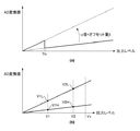
図7は、オフセット量(オフセット補正値)βの変動要因となるノイズが発生している条件下において、フレーム毎にオフセット補正値βを取得したときの、オフセット補正値βの変動を示すグラフである。同図において、横軸はフレーム数(時間に対応する)、縦軸はオフセット補正値βを示しており、オフセット補正値βのフレーム毎の変化をグラフAで示している。また、ノイズによる影響が無い状態の理想的な補正値(理想値)を、グラフCで示している。理想値は、不定期に発生するノイズ成分等による変動は発生しないが、撮像素子の駆動設定や、撮像素子の温度変化により変化する。第1の実施形態においては、撮像素子の駆動設定は同じままで、かつ温度も十分に安定した状態を想定している。 FIG. 7 is a graph showing the fluctuation of the offset correction value β when the offset correction value β is obtained for each frame under the condition where noise causing the fluctuation of the offset amount (offset correction value) β is generated. is there. In the figure, the horizontal axis indicates the number of frames (corresponding to time), and the vertical axis indicates the offset correction value β, and the change of the offset correction value β for each frame is indicated by the graph A. Further, a graph C shows an ideal correction value (ideal value) in a state where there is no influence by noise. The ideal value does not change due to noise components and the like that occur irregularly, but changes due to the drive setting of the imaging device and the temperature change of the imaging device. In the first embodiment, it is assumed that the drive setting of the imaging element remains the same and the temperature is sufficiently stable.
第1の実施形態においては、説明の便宜上、グラフCに示すように、オフセット補正値βの値が1〜100フレームまでの間、常に−5LSBとなるのが理想的であるものとする。また、グラフAの値が、理想値であるグラフCの値に対して±5LSBを超えた場合(−10LSB以下、もしくは0LSB以上)、画像上に信号レベルの段差が見え始めるものとする。 In the first embodiment, for convenience of explanation, as shown in the graph C, it is ideal that the value of the offset correction value β is always −5 LSB during 1 to 100 frames. In addition, when the value of the graph A exceeds ± 5 LSB (−10 LSB or less or 0 LSB or more) with respect to the value of the graph C which is the ideal value, it is assumed that the level difference of the signal level starts to be visible on the image.
図7に示す例では、グラフAの値が、理想値であるグラフCの値に対して、±5LSBを超えるフレームが多く存在する。つまり、あるフレームにおいては段差が見え、次のフレームでは段差が見えなくなるような映像が、何度も繰り返されていることになる。ここで、オフセット補正値βの変動を低減させる方法について具体的に説明する。 In the example shown in FIG. 7, there are many frames in which the value of graph A exceeds ± 5 LSB with respect to the value of graph C, which is an ideal value. In other words, an image in which a level difference can be seen in a certain frame and a level difference can not be seen in the next frame is repeated many times. Here, a method of reducing the fluctuation of the offset correction value β will be specifically described.
オフセット補正値βの変動を低減させる一つの方法として、下記の式(3)を用いてフィルタリング処理を行う方法がある。
βf(n)=β(n)×p+βf(n−1)×(1−p)
(0≦p≦1) …(3)
式(3)において、βf(n)は、nフレーム目におけるフィルタリング処理後のオフセット補正値である。また、nフレーム目に取得した画像を用いて、上記式(2)に基づいて算出された、新たなオフセット補正値をβ(n)、n−1フレーム目におけるフィルタリング処理後のオフセット補正値をβf(n−1)、巡回係数をp(0≦p≦1)と定義している。nの取り得る範囲は、n≧0であり、かつ、n=0の場合、前のフレームのオフセット補正値βf(−1)が存在しないため、p=1.0に設定した状態で、かつ、β(n−1)=0となるように設定する。
As one method of reducing the fluctuation of the offset correction value β, there is a method of performing a filtering process using the following equation (3).
βf (n) = β (n) × p + βf (n−1) × (1−p)
(0 ≦ p ≦ 1) (3)
In equation (3), β f (n) is an offset correction value after filtering processing in the nth frame. Also, using the image acquired at the nth frame, a new offset correction value calculated based on the above equation (2) is β (n), and the offset correction value after filtering processing at the n−1th frame is calculated. β f (n−1) and the cyclic coefficient are defined as p (0 ≦ p ≦ 1). The possible range of n is
上記式(3)において巡回係数p=0.1としたときのフィルタリング処理後のオフセット補正値βfの値の変化を、図7のグラフBで示している。同グラフから分かるように、グラフAに対してフィルタリング処理を行うことで、オフセット補正値βfの値が、画像上に信号レベルの段差が見え始める限界値である、グラフCから±5LSBの範囲内に収まっている。 The change of the value of the offset correction value βf after the filtering process when the cyclic coefficient p = 0.1 in the above equation (3) is shown by the graph B in FIG. As can be seen from the graph, by performing the filtering process on graph A, the value of offset correction value βf is within the range of ± 5 LSB from graph C, which is the limit value at which the level difference of the signal level begins to appear on the image. It is contained in
なお、図7に示す例では、巡回係数p=0.1としたが、必ずしも0.1である必要は無く、ノイズによる補正値の変動の大きさに合わせて、巡回係数を決定すれば良い。また、フィルタリング処理を行うための手段として、プログラムを用いて処理を行っても良いし、撮像素子1の内部もしくは画像処理部2にフィルタリング処理用の回路を追加で設けても良い。
In the example shown in FIG. 7, although the cyclic coefficient p is set to 0.1, it does not necessarily have to be 0.1, and the cyclic coefficient may be determined according to the magnitude of fluctuation of the correction value due to noise. . In addition, as means for performing filtering processing, processing may be performed using a program, or a circuit for filtering processing may be additionally provided inside the
上述したようにして得られた傾きの比α及びオフセット補正値βfを補正係数として用いて、以下の式(4)により、第二のランプ信号VRAMP(大)によりAD変換された第nフレームのS信号のデジタル信号SD(n)を補正し、補正後のデジタル信号S’D(n)を得る。
S’D(n)=SD(n)×α+βf …(4)
The slope ratio α obtained as described above and the offset correction value βf are used as a correction coefficient, and the following equation (4) is used to perform AD conversion of the second ramp signal VRAMP (large): The digital signal S D (n) of the S signal is corrected to obtain a corrected digital signal S ′ D (n).
S ′ D (n) = S D (n) × α + β f (4)
以上説明したように、ダミー画素の読み出し期間に固定電圧を読み出して得られる信号を用いて算出されたオフセット補正値βに対してフィルタリング処理を行う。これにより、オフセット補正値βの変動を、画像上に信号レベルの段差が見え始める限界値以下まで低減させることが可能となる。これにより、信号レベルの段差による画質劣化を低減することができる。 As described above, the filtering process is performed on the offset correction value β calculated using the signal obtained by reading out the fixed voltage during the readout period of the dummy pixel. As a result, it is possible to reduce the fluctuation of the offset correction value β below the limit value at which the step of the signal level starts to appear on the image. Thereby, it is possible to reduce the image quality deterioration due to the level difference of the signal level.
以下、好適なフィルタリング処理方法について、いくつかの例を挙げて説明する。 Hereinafter, preferred filtering methods will be described with some examples.
(1)オフセット補正値βが、瞬間的に大きく変動する場合
前述したように、列アンプ群130に供給している電源のノイズ、配線ノイズ、外乱ノイズにより補正値が変動した場合、巡回係数を小さくしてフィルタリング処理を行うことで、補正値の安定化を実現することができる。しかし、巡回係数pの値を小さくし過ぎると、急激な温度変化や、撮像素子の駆動方法の切替えにより理想値(補正目標値)が急激に変化した場合、オフセット補正値βf(n)の値が理想値付近まで収束するのに時間を要してしまう。また、巡回係数を大きくすると、フィルタリング処理による補正値の変動の低減効果が薄れてしまい、信号レベルの段差が見えるフレームが存在してしまう。
(1) When the offset correction value β fluctuates momentarily by a large amount As described above, when the correction value fluctuates due to noise of the power supply supplied to the
そこで、新たに取得したオフセット補正値β(n)が前のフレームにおけるフィルタリング処理後のオフセット補正値βf(n−1)に対して、明らかに大きく変動している場合は、巡回係数p=0に設定する。これにより、巡回係数pは、理想値の変動に対して十分に追従できる設定値となり、かつ外乱ノイズ等による補正値βの急激な変化も抑えることができ、ノイズによる影響を低減させることができる。特に外乱ノイズは、瞬間的に非常に大きなレベルの変動が発生することがあるため、フィルタリング処理後のオフセット補正値βf(n)が理想値付近まで収束する時間の最適化と、外乱ノイズ等に対するオフセット補正値の安定化が両立しない場合が出てくる。 Therefore, if the newly obtained offset correction value β (n) significantly fluctuates with respect to the offset correction value βf (n−1) after the filtering process in the previous frame, the cyclic coefficient p = 0 Set to As a result, the cyclic coefficient p is a set value that can sufficiently follow the variation of the ideal value, and also the rapid change of the correction value β due to disturbance noise etc. can be suppressed, and the influence of noise can be reduced. . In particular, disturbance noise may cause a very large level of fluctuation instantaneously, so optimization of the time for the offset correction value βf (n) after filtering to converge to near the ideal value, disturbance noise, etc. In some cases, stabilization of the offset correction value may not be compatible.
図8(a)は、外乱ノイズが発生した場合における、オフセット補正値βの変動を示すグラフである。同図に示す例では、図7に示す例に対して外乱ノイズが3フレーム分発生している場合を示しているが、それ以外は図7と同じであるため、図の詳細説明については省略する。 FIG. 8A is a graph showing the fluctuation of the offset correction value β when disturbance noise occurs. The example shown in the figure shows the case where disturbance noise is generated for three frames as compared with the example shown in FIG. 7, but the other parts are the same as FIG. 7 and thus detailed description of the figure is omitted. Do.
図8(a)は、グラフAの値が、理想値であるグラフCの値に対して、約60LSB程度高くなるフレームが3フレーム(13、43、73フレーム目)存在する。そのため、グラフBに示すように、フィルタリング処理を行ったにも関わらず、処理後の結果が、限界値であるグラフCから±5LSBを超えるフレームが発生する。つまり、100フレームの中で、段差が見えるフレームが数フレーム間だけ発生し、その後、段差が見えなくなるような映像が定期的に繰り返されることになる。 In FIG. 8A, there are three frames (13, 43, 73 frames) in which the value of the graph A becomes about 60 LSB higher than the value of the graph C which is the ideal value. Therefore, as shown in the graph B, although the filtering process is performed, a frame after ± 5 LSB is generated from the graph C which is the limit value after the process. That is, in 100 frames, a frame in which a level difference can be seen occurs only for a few frames, and thereafter, an image in which the level difference can not be seen is periodically repeated.
そこで、第1の実施形態では、上記式(3)を用いてフィルタリング処理を行う前に、新たに取得したオフセット補正値β(n)と、前フレームまでの補正値のフィルタリング処理結果βf(n−1)との差分を求める。そして、その差分が閾値を超えたかどうかを判定し、閾値を超えていた場合には、巡回係数p=0に設定する制御を行う。第1の実施形態においては、閾値を±30LSBに設定するが、外乱ノイズが発生しない時のノイズレベル(電源電圧やパターン配線起因のランダムな変動)と、巡回係数の設定値に応じて閾値を決定すると良い。理想的には、外乱ノイズが発生した場合でも、フィルタリング処理後のオフセット補正値βf(n)が、画像上に信号レベルの段差が見え始める限界値を超えないような閾値にするのが好ましい。 Therefore, in the first embodiment, before performing the filtering process using the above equation (3), the newly obtained offset correction value β (n) and the filtering process result βf (n of the correction values up to the previous frame) Calculate the difference from -1). Then, it is determined whether the difference exceeds the threshold, and if it exceeds the threshold, control is performed to set the cyclic coefficient p = 0. In the first embodiment, the threshold is set to ± 30 LSB, but the threshold is set according to the noise level (random fluctuation due to the power supply voltage and pattern wiring) when disturbance noise is not generated and the set value of the cyclic coefficient. You should decide. Ideally, even if disturbance noise occurs, it is preferable to set the threshold value so that the offset correction value βf (n) after the filtering process does not exceed the limit value at which the step of the signal level starts to be visible on the image.
図8(b)のグラフBに、閾値判定を追加した場合における、フィルタリング処理結果を示している。同図では、閾値を±30LSBとしており、外乱ノイズが発生した3フレームについては、巡回係数p=0となり、前フレームにおけるフィルタリング処理後の補正値βf(nー1)が引き継がれる。本処理を追加することにより、フィルタリング処理後のオフセット補正値βf(n)が全て画像上に信号レベルの段差が見え始める限界値以下の範囲に収まる。 The graph B in FIG. 8B shows the result of the filtering process when the threshold determination is added. In the figure, the threshold value is ± 30 LSB, and the cyclic coefficient p = 0 for three frames in which disturbance noise is generated, and the correction value βf (n−1) after the filtering process in the previous frame is taken over. By adding this process, all the offset correction values βf (n) after the filtering process fall within the range below the limit value at which the step of the signal level starts to be visible on the image.
以上説明したように、フィルタリング処理を行う前に、前フレームにおけるフィルタリング処理後のオフセット補正値βf(n−1)と、新たに取得したオフセット補正値β(n)との差分を求める。そして、その差分値が閾値を超えたかどうかを判定し、閾値を超えていた場合には巡回係数p=0にする。これにより、外乱ノイズ等により瞬間的に大きな変動が生じた場合に、フィルタリング処理後のオフセット補正値βf(n)が影響を受けるのを抑えることができる。更に、フィルタリング処理後のオフセット補正値βf(n)が理想値付近まで収束するまでの時間の最適化と、外乱ノイズ等に対する補正値の安定化を両立させることができる。 As described above, before performing the filtering process, the difference between the offset correction value βf (n−1) after the filtering process in the previous frame and the newly acquired offset correction value β (n) is obtained. Then, it is determined whether the difference value exceeds the threshold, and if it exceeds the threshold, the cyclic coefficient p is set to 0. This makes it possible to suppress the influence of the offset correction value βf (n) after the filtering process when a large change occurs instantaneously due to disturbance noise or the like. Furthermore, it is possible to achieve both optimization of the time until the offset correction value βf (n) after the filtering process converges to near the ideal value and stabilization of the correction value for disturbance noise and the like.
また、本実施形態においては外乱ノイズを扱ったが、同様のノイズを発生させるもの全てについて適用可能である。 Further, although disturbance noise is dealt with in the present embodiment, the present invention is applicable to all noise generating similar noises.
(2)電源起動時、及び撮像素子の駆動方法を切替えた場合
電源起動時は、映像信号の出力が安定していないことや、起動時における各種処理を行うために撮像素子1の駆動方法の切替えが発生することがあるため、理想値が大きく変化する可能性がある。また、電源起動後においても撮像素子の駆動方法が切替えられた場合、切替え直後に理想値が瞬間的に大きく変わる。上記要因により、フィルタリング処理後のオフセット補正値βf(n)と理想値との差が瞬間的に大きくなってしまう。
(2) When the power source is turned on and when the driving method of the imaging element is switched When the power is turned on, the output of the video signal is not stable and the driving method of the
フィルタリング処理を行わなければ、理想値付近に収束するまでの時間を最短にすることが可能である。しかしながら、フィルタリング処理を行わなければ、オフセット補正値βf(n)が理想値付近に収束した後、電源ノイズなどによる補正値β(n)の変動を低減することができなくなる。 If the filtering process is not performed, it is possible to minimize the time until convergence to the vicinity of the ideal value. However, if the filtering process is not performed, after the offset correction value βf (n) converges near the ideal value, it is not possible to reduce the fluctuation of the correction value β (n) due to power supply noise or the like.
そこで、本実施形態においては、フィルタリング処理を行う前に、新たに取得した補正値β(n)と、前フレームにおけるフィルタリング処理後のオフセット補正値βf(n−1)との差分を求め、その差分値の大きさに応じて巡回係数を変更する。具体的には、差分値が大きい場合は巡回係数を高めに設定し、差分値が小さい場合は巡回係数を低めに設定する。差分値に対する巡回係数の決め方として、理想値の変化の大きさや、電源ノイズ等による補正値の変動の大きさに応じて決定すれば良い。 Therefore, in the present embodiment, before performing the filtering process, the difference between the newly acquired correction value β (n) and the offset correction value βf (n−1) after the filtering process in the previous frame is obtained, and The cyclic coefficient is changed according to the magnitude of the difference value. Specifically, if the difference value is large, the cyclic coefficient is set higher, and if the difference value is small, the cyclic coefficient is set lower. As a method of determining the cyclic coefficient with respect to the difference value, it may be determined according to the magnitude of the change of the ideal value and the magnitude of the fluctuation of the correction value due to the power supply noise and the like.
本実施形態においては、図9(a)に示すテーブルデータを予め設け、これを参照して、新たに取得したオフセット補正値β(n)と、前フレームにおけるフィルタリング処理後のオフセット補正値βf(n−1)との差分値に対応する巡回係数pを決定する。図9(a)のテーブルデータに示した差分値は、理想的(電源ノイズ等による補正値の変化が無い場合)には、オフセット補正値が1フレーム以内に画像上に信号レベルの段差が見え始める限界値以下に収束するような設定値にしている。また、図9(a)においては説明の便宜上、正の差分値のみをテーブルデータとして設けたが、負の差分値も同様であり、厳密には絶対値|β(n)−βf(n−1)|となる。 In the present embodiment, the table data shown in FIG. 9A is provided in advance, and with reference to this, the newly obtained offset correction value β (n) and the offset correction value βf after the filtering process in the previous frame A cyclic coefficient p corresponding to the difference value with n−1) is determined. The difference value shown in the table data of FIG. 9A is ideally (when there is no change in the correction value due to power supply noise etc.), the offset correction value shows a step of the signal level on the image within one frame. The set value is to converge below the limit value to be started. Further, in FIG. 9A, for convenience of explanation, only positive difference values are provided as table data, but negative difference values are also the same. Strictly speaking, absolute value | β (n) −βf (n− 1) |
図9(b)は、撮像素子1の駆動方法を切替える前後における、図9(a)のテーブルデータに基づいた巡回係数の設定値と、オフセット補正差分値β(n)−βf(n−1)の変化について表した図である。同図において、オフセット補正差分値に応じて、巡回係数の設定値を変更した場合のグラフを実線、巡回係数の設定値を変更しない場合のグラフを破線で示している。また、画像上に信号レベルの段差が見え始める限界値である10LSBについても参考として記載している。
FIG. 9B shows the setting value of the cyclic coefficient based on the table data of FIG. 9A and the offset correction difference value β (n) −βf (n−1 before and after switching the driving method of the
同図において、撮像素子1の駆動方法を切替える前は、オフセット補正差分値がほぼ0LSBに近い状態(厳密には、電源ノイズ等に起因する変動が重畳している)なので、巡回係数p=0.1に設定している。撮像素子1の駆動方法を切替えるまでの期間は、巡回係数pは常に0.1に設定されたままである。
In the same figure, before switching the driving method of the
撮像素子1の駆動方法を切替える際の制御について説明する。切替え直後のフレーム(1フレーム目)では、60LSBのオフセット補正差分値が発生しているため、図9(a)のテーブルデータに基づき、巡回係数p=0.9に設定する。そうすることで、駆動方法の切替え直後のフレームでも、駆動方法切替え後の理想値に近い補正値を取得することができる。本実施形態においては、巡回係数を変更することにより、理想的(電源ノイズ等による補正値の変化が無い場合)には、10LSB以下まで低減することができる。
Control at the time of switching the driving method of the
駆動方法の切替え後、2フレーム目において、オフセット補正差分値が10LSBとなったため、図9(a)のテーブルデータに基づいて、巡回係数p=0.1に設定する。これ以降のフレームについても、オフセット補正差分値が10LSB以下の場合には巡回係数pを常に0.1に設定することになる。 After the switching of the driving method, the offset correction difference value becomes 10 LSB in the second frame, so the cyclic coefficient p is set to 0.1 based on the table data of FIG. 9A. Also for the subsequent frames, if the offset correction difference value is 10 LSB or less, the cyclic coefficient p is always set to 0.1.
これに対し、巡回係数p=0.1の設定を維持した状態で駆動方法を切替えた場合、オフセット補正差分値を画像上に信号レベルの段差が見え始める限界値以下に収束させるためには、18フレーム必要であった。しかし、オフセット補正差分値を求め、その大きさに応じて巡回係数pを変えることにより、1フレーム後には限界値以下となり、理想値付近に収束した後は、電源ノイズ等による補正値の変動を低減させることができる。 On the other hand, when the driving method is switched while maintaining the setting of the cyclic coefficient p = 0.1, in order to cause the offset correction difference value to converge below the limit value at which the signal level difference starts to be visible on the image: 18 frames were required. However, the offset correction difference value is obtained, and by changing the cyclic coefficient p according to the magnitude, the value becomes less than the limit value after one frame, and after convergence near the ideal value, fluctuation of the correction value due to power supply noise etc. It can be reduced.
以上説明したように、電源起動時、及び撮像素子の駆動方法を切替えた場合に、フィルタリング処理を行う前に、オフセット補正値β(n)とβf(n−1)の差分を求め、その差分値の大きさに応じて巡回係数を変更する。これにより、フィルタリング処理後のオフセット補正値βf(n)と理想値との差が瞬間的に大きくなっても、オフセット補正値βf(n)の収束時間を短縮することができる。また、オフセット補正値βf(n)が理想値付近に収束した後には、電源ノイズ等に起因する補正値の変動を低減させることができる。 As described above, the difference between the offset correction values β (n) and βf (n−1) is obtained before the filtering process at the time of power activation and when the driving method of the imaging device is switched, and the difference Change the cyclic coefficient according to the value of the value. Thus, even if the difference between the offset correction value βf (n) after filtering processing and the ideal value instantaneously increases, the convergence time of the offset correction value βf (n) can be shortened. In addition, after the offset correction value βf (n) converges near the ideal value, it is possible to reduce the fluctuation of the correction value caused by the power supply noise and the like.
(3)温度が変化した場合
オフセット補正値の理想的な値が変化する要因の一つとして、撮像素子1の温度変化がある。特に、電源起動後に撮像素子1が駆動し始めた際に、電力が撮像素子1内で消費し始めることにより急激に温度が上昇したり、この温度上昇を抑えるために、ファンやペルチェ素子などの冷却装置を用いて冷却が行われることで急激に温度が降下することがある。このような急激な温度変化により、オフセット補正値の理想値が急激に変化する可能性がある。
(3) When Temperature Changes A temperature change of the
このように理想値が急激に変化した場合、前述したように、電源電圧変動やパターン配線ノイズなどに起因するオフセット補正値βf(n)の変動を抑えるために巡回係数を低めに設定してフィルタリング処理を行った場合、理想値に追従できない可能性がある。 Thus, when the ideal value changes rapidly, as described above, in order to suppress the fluctuation of the offset correction value β f (n) caused by the power supply voltage fluctuation, pattern wiring noise, etc. When processing is performed, there is a possibility that the ideal value can not be followed.
そこで実施形態においては、サーミスタや温度検出センサ等を用いて測定した温度から、フレーム間の温度変化を検出し、温度の変化率に応じて巡回係数を変える処理を行う。具体的には、温度の変化率が大きい場合には巡回係数を高めに設定し、温度の変化率が小さい場合には巡回係数を低めに設定する。これにより、急激な温度変化により理想値が急激に変化した場合でも、オフセット補正値βf(n)が理想値に対して追従し、かつ理想値が急激に変化することが無い場合においては、電源ノイズ等によるオフセット補正値β(n)の変動を低減させることができる。 Therefore, in the embodiment, a temperature change between frames is detected from a temperature measured using a thermistor, a temperature detection sensor or the like, and a process of changing a cyclic coefficient in accordance with a temperature change rate is performed. Specifically, if the rate of change of temperature is large, the cyclic coefficient is set high, and if the rate of change of temperature is small, the cyclic coefficient is set low. As a result, even if the ideal value changes rapidly due to a rapid temperature change, the offset correction value βf (n) follows the ideal value and the power supply does not change rapidly. The variation of the offset correction value β (n) due to noise or the like can be reduced.
図10は、時間(フレーム)変化に対する、温度、温度変化率、巡回係数の設定値を表したイメージ図である。同図において、温度とは、サーミスタや温度検出センサにより取得された温度の値を示している。温度変化率とは、単位時間(本実施形態では、フレーム)あたりに増加した温度変化量(温度のグラフの微分値)を表している。本実施形態においては、温度変化率が高い順に、A〜Eの領域に分けているが、実際に制御を行う場合は、温度変化量を単位時間で除算した数値を用いると良い。巡回係数の設定値は、温度変化率A〜Eに対する巡回係数の設定値を示している。本実施形態においては、温度変化率A=0.5、温度変化率B=0.4、温度変化率C=0.3、温度変化率D=0.2、温度変化率E=0.1が対応している。 FIG. 10 is an image diagram showing setting values of the temperature, the temperature change rate, and the cyclic coefficient with respect to the time (frame) change. In the figure, the temperature indicates the value of the temperature acquired by a thermistor or a temperature detection sensor. The temperature change rate represents a temperature change amount (differential value of a graph of temperature) increased per unit time (in the present embodiment, a frame). In the present embodiment, the regions are divided into areas A to E in descending order of the temperature change rate. However, when control is actually performed, it is preferable to use a numerical value obtained by dividing the temperature change amount by unit time. The set value of the cyclic coefficient indicates the set value of the cyclic coefficient with respect to the temperature change rates A to E. In the present embodiment, the temperature change rate A = 0.5, the temperature change rate B = 0.4, the temperature change rate C = 0.3, the temperature change rate D = 0.2, and the temperature change rate E = 0.1. Is supported.
図10において、起動直後からt1までの期間は、温度変化率がBの領域であるので、巡回係数の設定値を0.4に設定する。t1からt2までの期間は、温度変化率がCの領域であるので、巡回係数の設定値を0.3に設定する。t2からt3までの期間は、温度変化率がDの領域であるので、巡回係数の設定値を0.2に設定する。t3以降は、温度変化率がEの領域であるので、巡回係数の設定値を0.1にする。 In FIG. 10, since the temperature change rate is in the region of B during the period from immediately after the start to t1, the set value of the cyclic coefficient is set to 0.4. Since the temperature change rate is in the region of C during the period from t1 to t2, the set value of the cyclic coefficient is set to 0.3. In the period from t2 to t3, since the temperature change rate is in the region of D, the setting value of the cyclic coefficient is set to 0.2. After t3, since the temperature change rate is in the region of E, the set value of the cyclic coefficient is set to 0.1.
このように、温度の変化率が大きい場合には巡回係数を高くし、温度の変化率が小さい場合には巡回係数を低くする。これにより、急激な温度変化により理想値が急に変化した場合でも、フィルタリング処理後のオフセット補正値βf(n)が理想値に対して追従する。また、理想値が急激に変化することが無い場合においては、電源ノイズ等によるオフセット補正値βf(n)の変動を低減させることができる。 As described above, when the rate of change of temperature is large, the cyclic coefficient is increased, and when the rate of change of temperature is small, the cyclic coefficient is decreased. As a result, even when the ideal value suddenly changes due to a rapid temperature change, the offset correction value βf (n) after the filtering process follows the ideal value. In addition, in the case where the ideal value does not change rapidly, it is possible to reduce the fluctuation of the offset correction value βf (n) due to power supply noise or the like.
なお、図10に示す例では、温度が上昇する場合について示しているが、温度が下降する場合も同様であり、厳密には、温度変化率の絶対値に応じて循環係数の設定値を設定する。 Although the example shown in FIG. 10 shows the case where the temperature rises, the same applies to the case where the temperature falls, and strictly speaking, the setting value of the circulation coefficient is set according to the absolute value of the temperature change rate. Do.
(4)被写体のコントラスト
オフセット補正値β(n)が変動した場合に画像上に信号レベルの段差が見えるが、被写体のコントラストと明るさによって、目立ち易さが変わる。図11は、1フレーム分の画像の輝度分布を表すヒストグラムを示しており、横軸は信号レベル、縦軸は1フレームの画面内において発生した輝度の頻度(画素数)を示している。また、判定レベルVsとは、前述したとおり、第一のランプ信号VRAMP(大)と第二のランプ信号VRAMP(小)の切替えが行われる信号レベルを表している。
(4) Contrast of subject Although the level difference of the signal level is visible on the image when the offset correction value β (n) fluctuates, the conspicuousness changes depending on the contrast and the brightness of the subject. FIG. 11 shows a histogram representing the luminance distribution of an image of one frame, the horizontal axis representing the signal level, and the vertical axis representing the frequency (number of pixels) of luminance generated within the screen of one frame. Further, as described above, the determination level Vs represents a signal level at which the switching between the first ramp signal VRAMP (large) and the second ramp signal VRAMP (small) is performed.
図11(a)のようなヒストグラムになる画像には、判定レベルVs近傍の輝度を有する画素が多く存在している。つまり、コントラストが低く、判定レベルVs近傍の輝度レベルを中心に、徐々に明るさが変化する被写体である可能性が高いことが推測される。よって、このような画像は、判定レベルVs近傍の輝度を有する画素の発生頻度が高く、信号レベルの段差が見え易い画像であることが分かる。このような画像に対しては、オフセット補正値βf(n)をできるだけ安定させるために、巡回係数を低めに設定するのが好ましい。 In an image to be a histogram as shown in FIG. 11A, a large number of pixels having luminance in the vicinity of the determination level Vs are present. That is, it is estimated that the possibility of the subject being low in contrast and having a gradually changing brightness around the luminance level near the determination level Vs is high. Therefore, it can be seen that such an image is an image in which the frequency of occurrence of pixels having luminance near the determination level Vs is high and the level difference of the signal level can be easily seen. For such an image, in order to stabilize the offset correction value βf (n) as much as possible, it is preferable to set a lower cyclic coefficient.
一方、図11(b)のようなヒストグラムになる画像は、判定レベルVs近傍の画素が、突出して多く存在している訳では無い。つまり、コントラストが高く、画面全体に万遍なく様々な輝度が存在するような被写体であることが推測される。このような画像は、判定レベルVs近傍の輝度を有する画素の発生頻度が低く、信号レベルの段差が見え難い画像であることが分かる。このような画像に対しては、オフセット補正値βf(n)を安定化させる必要性は低く、巡回係数を高めに設定することで、理想値への追従性を良くするのが好ましい。 On the other hand, in an image to be a histogram as shown in FIG. 11B, many pixels in the vicinity of the determination level Vs are not necessarily prominently present. That is, it is presumed that the subject is high in contrast, and has various luminances all over the screen. It can be seen that such an image is an image in which the frequency of occurrence of pixels having luminance in the vicinity of the determination level Vs is low and the level difference of the signal level is difficult to see. For such an image, it is less necessary to stabilize the offset correction value βf (n), and it is preferable to improve the followability to the ideal value by setting the cyclic coefficient higher.
本実施形態においては、ヒストグラム(輝度分布)に応じて、最適な巡回フィルタの係数を決定する。具体的には、判定レベルVs近傍の信号レベルの画素に対して重み付けを行い、重み付けされた画素の発生数だけ積算した、重み付け積算値を算出することで、判定レベルVs近傍の画素がどれだけ存在したかを求める。そして、重み付け積算値の値に応じてフィルタリング処理における巡回係数の設定値を決定する。 In the present embodiment, the optimum coefficient of the cyclic filter is determined according to the histogram (brightness distribution). Specifically, weighting is performed on pixels at the signal level in the vicinity of the determination level Vs, and by calculating a weighted integration value obtained by integrating only the number of occurrences of the weighted pixels, how many pixels in the vicinity of the determination level Vs are Find out if it exists. Then, the set value of the cyclic coefficient in the filtering process is determined according to the value of the weighted integrated value.
図12(a)は、重み付けを行う際に用いる重み付け係数の一例を示す。横軸が信号レベルで、縦軸が重み付け係数を示している。同図において、判定レベルVsの信号レベルの係数を1.0とし、判定レベルVsに対して信号レベルの差分が大きくなるにつれて、重み付け係数を小さくしていく。判定レベルVsの重み付係数に対する信号レベルの差がある程度大きい場合は、信号レベルの段差が影響する可能性が低いため、重み付係数を0に設定する。なお、重み付け係数を0に設定する信号レベルを決定する際には、S信号レベル近傍で発生し得る電源ノイズ等によるオフセット補正値β(n)の変動の大きさを考慮すれば良い。 FIG. 12A shows an example of a weighting factor used when performing weighting. The horizontal axis is the signal level, and the vertical axis is the weighting factor. In the figure, the coefficient of the signal level of the determination level Vs is 1.0, and the weighting coefficient is reduced as the difference of the signal level with respect to the determination level Vs increases. If the difference between the signal level and the weighting factor of the determination level Vs is large to some extent, the weighting factor is set to 0 because the possibility of being affected by the level difference of the signal level is low. When determining the signal level for setting the weighting factor to 0, the magnitude of the fluctuation of the offset correction value β (n) due to power supply noise or the like that may occur near the S signal level may be taken into consideration.
上記方法にて重み付けされた各画素に対して、画素数分だけ積算していくことで、重み付け積算値が算出される。この算出された積算値に応じて、フィルタリング処理における巡回係数の設定値を決定する。 A weighted integration value is calculated by integrating each pixel weighted by the above method by the number of pixels. In accordance with the calculated integrated value, the set value of the cyclic coefficient in the filtering process is determined.
図12(b)は、重み付け積算値に対する巡回係数の設定値を示したイメージ図である。横軸が重み付け積算値を示しており、縦軸が巡回係数の設定値を示している。同図に示すように、重み付け積算値が大きくなるにつれて、巡回係数の設定値は低くなる。 FIG. 12B is an image diagram showing setting values of cyclic coefficients with respect to weighted integrated values. The horizontal axis indicates the weighted integrated value, and the vertical axis indicates the set value of the cyclic coefficient. As shown in the figure, as the weighted integrated value increases, the setting value of the cyclic coefficient decreases.
上記処理を行うことで、信号レベルの段差が被写体として見え易いものであるかどうかを判定し、判定結果に応じて巡回係数の設定値を変更する。これにより、撮影した被写体の輝度分布に応じて、オフセット補正値βf(n)の安定化と、理想値への追従性を最適化することができる。 By performing the above processing, it is determined whether or not the step of the signal level is easily seen as a subject, and the setting value of the cyclic coefficient is changed according to the determination result. Thus, the stabilization of the offset correction value βf (n) and the followability to the ideal value can be optimized in accordance with the luminance distribution of the photographed subject.
また、本実施形態においては、画面全体のヒストグラムを用いて説明したが、画面内の複数の領域に分割してヒストグラムを作成しても良い。そうすることで、画面内のある領域では段差が発生しやすく、ある領域では発生し難いような被写体においても、上記した最適化をより精度良く実現することができる。 Further, although the present embodiment has been described using the histogram of the entire screen, the histogram may be created by dividing it into a plurality of areas in the screen. By doing so, the above-described optimization can be realized with higher accuracy even for a subject that is likely to have a step in a certain area in the screen and hard to occur in a certain area.
以上説明したように、判定レベル近傍の信号レベルの画素に対して重み付けを行い、重み付けされた画素の発生数だけ積算した重み付け積算値を算出し、その積算値の結果に応じて巡回係数の設定値を変更する。これにより、撮影した被写体の輝度分布に応じて、補正値の安定化と、理想値への追従性を最適化することができる。 As described above, weighting is performed on pixels at the signal level near the determination level, a weighted integration value is calculated by integrating the number of occurrences of the weighted pixels, and a cyclic coefficient is set according to the result of the integration value. Change the value Thereby, the stabilization of the correction value and the followability to the ideal value can be optimized according to the luminance distribution of the photographed subject.
(5)フレームレート
前述したように、理想値は、温度変化に応じて変化する。その理想値に対してオフセット補正値βf(n)を追従させるためには、オフセット補正値β(n)を頻繁に取得し、オフセット補正値βf(n)を更新していく必要がある。
(5) Frame rate As described above, the ideal value changes in accordance with the temperature change. In order to make the offset correction value βf (n) follow the ideal value, it is necessary to frequently acquire the offset correction value β (n) and update the offset correction value βf (n).
しかし、低フレームレート時においては、オフセット補正値β(n)の取得が頻繁に行えないため、フレームレートによっては、オフセット補正値βf(n)が理想値の変化に追従するのが遅れてしまう可能性がある。特に、電源ノイズ等によるオフセット補正値β(n)の変動が大きい場合、巡回係数を低めに設定する必要があるため、急激な温度変化による理想値の変動に対して、オフセット補正値βf(n)の追従が遅れてしまう。そこで、本実施形態では、フレームレートに応じて、巡回係数の設定値を変更する。 However, at a low frame rate, acquisition of the offset correction value β (n) can not be frequently performed, and therefore, depending on the frame rate, the offset correction value βf (n) delays to follow the change in the ideal value. there is a possibility. In particular, when the fluctuation of the offset correction value β (n) due to power supply noise or the like is large, it is necessary to set the cyclic coefficient lower. Therefore, the offset correction value βf (n ) Is delayed. Therefore, in the present embodiment, the setting value of the cyclic coefficient is changed according to the frame rate.
図13は、フレームレートに対する巡回係数pの設定値を示している。フレームレートが低いほど、巡回係数pの設定値は大きくなり、フレームレートが高くなるにつれて巡回係数pの設定値は小さくなる。つまり、単位時間あたりに取得できるオフセット補正値β(n)の数が少ないほど、新たに取得したオフセット補正値β(n)がフィルタリング処理後のオフセット補正値βf(n)に与える影響度が大きくなる。よって、フレームレートが低いほど、温度変化による理想値の変動に対して追従し易くなる。各巡回係数に対するフレームレートの範囲は、温度変化率と、電源ノイズ等によるオフセット補正値β(n)の変動を考慮して決めればよい。 FIG. 13 shows setting values of the cyclic coefficient p with respect to the frame rate. As the frame rate is lower, the setting value of the cyclic coefficient p is larger, and as the frame rate is higher, the setting value of the cyclic coefficient p is smaller. That is, as the number of offset correction values β (n) that can be acquired per unit time decreases, the degree of influence of the newly acquired offset correction value β (n) on the offset correction value βf (n) after the filtering process increases. Become. Therefore, the lower the frame rate, the easier it is to follow fluctuations in the ideal value due to temperature changes. The range of the frame rate for each cyclic coefficient may be determined in consideration of the temperature change rate and the fluctuation of the offset correction value β (n) due to power supply noise or the like.
以上説明したように、フレームレートに応じて巡回係数の設定値を変更することで、補正値の更新頻度が少ない低フレームレート時においても、理想値の変動に対する追従性と、オフセット補正値の安定化を最適化することができる。 As described above, by changing the setting value of the cyclic coefficient according to the frame rate, the followability to the change of the ideal value and the stability of the offset correction value even at the low frame rate where the update frequency of the correction value is low. Can be optimized.
(6)映像として使用しないフレームがある場合
フレームレートに応じて巡回係数を変更する場合について前述したが、撮像素子1の処理によっては、撮像素子1から画像を読み出すが、実際に出力画像としては用いない場合がある。例えば、120fpsで撮像素子1から画像を読み出し、30fpsで映像出力されるとする。この場合、4フレーム分の画像のうち、1枚の画像しか実際の画像としては使用されない。
(6) When there is a frame not used as an image Although the case where the cyclic coefficient is changed according to the frame rate has been described above, depending on the processing of the
前述したように、できるだけ高い頻度でオフセット補正値を取得した方が、フィルタリング処理による補正値の安定化を実現できるため、映像出力として使用しないフレームの画像についても補正値β(n)を算出し、フィルタリング処理に用いる。具体的には、映像出力として用いるフレームのオフセット補正値β(n)のみを用いてフィルタリング処理した結果と、フレームの補正値β(n)に加えて、映像出力として用いないフレームのオフセット補正値β(n)も用いてフィルタリング処理した結果の差分を取る。これにより、オフセット補正値β(n)の安定度を判定する。上記差分が大きければ安定していないと判定され、上記差分が小さければ安定していると判定される。 As described above, since acquiring the offset correction value as frequently as possible can realize stabilization of the correction value by the filtering process, the correction value β (n) is calculated also for an image of a frame not used as a video output. , Used for filtering processing. Specifically, the offset correction value of a frame not used as a video output in addition to the result of filtering processing using only the frame offset correction value β (n) used as a video output and the frame correction value β (n) Take the difference of the filtering result using β (n). Thereby, the stability of the offset correction value β (n) is determined. If the difference is large, it is determined to be unstable. If the difference is small, it is determined to be stable.
上記判定結果により、安定度が高い場合には、電源ノイズ等による補正値の変動が小さいため、追従性を早くするために巡回係数を高めに設定する。一方、安定度が低い場合には、電源ノイズ等によるオフセット補正値の変動が大きいため、巡回係数を低めに設定する。 According to the above determination result, when the degree of stability is high, the fluctuation of the correction value due to power supply noise or the like is small, so the cyclic coefficient is set high in order to accelerate the followability. On the other hand, when the degree of stability is low, since the fluctuation of the offset correction value due to power supply noise or the like is large, the cyclic coefficient is set to a lower value.
本実施形態では、映像出力するフレームのみを用いてフィルタリング処理を行ったときのオフセット補正値をβf(n)とし、映像出力しないフレームも用いてフィルタリング処理を行ったときのオフセット補正値をβf´(n)とする。そして、安定度を判定するために、βf(n)−βf´(n)を算出する。 In this embodiment, the offset correction value when the filtering process is performed using only the frames for video output is βf (n), and the offset correction value when the filtering process is performed using the frames for which the video output is not performed is βf ′. (N) Then, to determine the degree of stability, βf (n) −βf ′ (n) is calculated.
図14(a)は、時間(フレーム)変化に対する、オフセット補正値β(n)と、映像出力する画像のみを用いてフィルタリング処理を行ったときのオフセット補正値βf(n)と、映像出力しない画像も用いてフィルタリング処理を行ったときのオフセット補正値βf´(n)と、安定度を表すβf(n)−βf´(n)を示したグラフである。 In FIG. 14A, the offset correction value β (n) with respect to the time (frame) change and the offset correction value βf (n) when the filtering process is performed using only the image output image are not output It is the graph which showed offset correction value (beta) f '(n) when performing a filtering process also using the image, and (beta) f (n)-(beta) f' (n) showing stability.
同図において、横軸は時間(フレーム表記で、期間は1〜100フレーム)を示し、縦軸はオフセット補正値β(n)、βf(n)、βf´(n)、及びオフセット補正差分値βf(n)−βf´(n)を示している。本実施形態においては、映像出力する画像のみを用いてフィルタリング処理を行った時のオフセット補正値βf(n)は、巡回係数を高めに設定している。一方、映像出力しない画像も用いてフィルタリング処理を行ったときのオフセット補正値βf´(n)は、できるだけ安定した補正値を取得するために(安定度を判定するための基準となるため)、巡回係数を最も低い設定にしている。このときの差分値βf(n)−βf´(n)が大きければ大きいほど、βf(n)が安定していないことになる。 In the figure, the horizontal axis indicates time (in frame notation, a period is 1 to 100 frames), and the vertical axis indicates offset correction values β (n), βf (n), βf '(n), and offset correction difference values. (beta) f (n)-(beta) f '(n) is shown. In this embodiment, the offset correction value β f (n) when the filtering process is performed using only the image to be video output is set to have a high cyclic coefficient. On the other hand, the offset correction value βf ′ (n) when the filtering process is performed using an image which does not output a video is to obtain a correction value as stable as possible (because it becomes a reference for determining the stability), The cyclic coefficient is set to the lowest. As the difference value βf (n) -βf '(n) at this time is larger, βf (n) is less stable.
本実施形態では、図14(b)に示すように、差分値βf(n)−βf´(n)の大きさに応じた、巡回係数pに乗算するための乗算値qの値をテーブルデータとして持ち、このテーブルデータに基づいて、巡回係数pに乗算値qを乗算する処理を行う。こうすることで、映像出力する画像のみを用いてフィルタリング処理を行ったときのオフセット補正値βf(n)を算出するために用いる巡回係数が、安定度の観点から適正でない場合に、巡回係数を最適化させることができる。なお、図14(b)においては説明の便宜上、正の差分値のみをテーブルデータとして設けたが、負の差分値も同様であり、厳密には絶対値|βf(n)−βf´(n)|となる。 In the present embodiment, as shown in FIG. 14B, the value of the multiplication value q for multiplying the cyclic coefficient p according to the magnitude of the difference value βf (n) −βf ′ (n) is table data , And based on the table data, the cyclic coefficient p is multiplied by the multiplication value q. By doing this, if the cyclic coefficient used to calculate the offset correction value βf (n) when the filtering process is performed using only the image to be output is not appropriate from the viewpoint of stability, the cyclic coefficient is It can be optimized. In FIG. 14B, only positive difference values are provided as table data for convenience of explanation, but negative difference values are also the same. Strictly speaking, absolute value | β f (n)-β f '(n It becomes |).
以上説明したように、映像出力として用いるフレームの補正値β(n)のみを用いてフィルタリング処理した結果と、フレームの補正値β(n)に加えて、映像出力として用いないフレームの補正値β(n)も用いてフィルタリング処理した結果の差分を取る。そして、映像出力として用いるフレームの補正値の安定度を求め、安定度に応じて巡回係数を変更することにより、巡回係数を最適化することができる。 As described above, in addition to the result of filtering using only the correction value β (n) of the frame used as the video output, and the correction value β (n) of the frame, the correction value β of the frame not used as the video output. (N) is also used to take the difference of the filtered result. Then, by determining the stability of the correction value of the frame used as the video output and changing the cyclic coefficient according to the stability, it is possible to optimize the cyclic coefficient.
(7)被写体の動き
電源ノイズ等による補正値β(n)の変動に起因して発生するレベル段差の見え方は、被写体によって目立ち方が変わる。特に、動画の場合は、被写体に動きが無い状態だと見え易いが、被写体に動きがあると、各画素の信号レベルが常に変化していることが多いため、目立ち難くなる。
(7) Movement of Subject The manner in which the level difference appears due to the fluctuation of the correction value β (n) due to power supply noise or the like changes depending on the subject. In particular, in the case of a moving image, it is easy to see that the subject has no motion, but when there is motion in the subject, the signal level of each pixel often changes constantly, making it less noticeable.
そこで、本実施形態においては、被写体の動き量に応じて巡回係数を決定する処理を行う。動き量を検出するには、一般的に用いられている、ジャイロセンサを用いる方法や、取得した画像から動きベクトルを算出し、動き量を検出する方法などがある。被写体の動き量の検出については、既知の技術を用いて検出するものとし、詳細については説明を省略する。 Therefore, in the present embodiment, processing is performed to determine a cyclic coefficient according to the amount of movement of the subject. In order to detect the amount of movement, there are a generally used method of using a gyro sensor, a method of calculating a motion vector from the acquired image, and a method of detecting the amount of movement. The detection of the amount of movement of the subject is detected using a known technique, and the description thereof is omitted.
図15は、被写体の動き量に対する、巡回係数に乗算する乗算値qを表したテーブルデータである。本実施形態においては、被写体の動き量が小さい場合を基準(1.0倍)として、被写体の動き量が大きくなるにつれて巡回係数を高くし、オフセット補正値βf(n)が理想値に対して追従し易くなるような処理を行う。なお、本実施形態においては、被写体の動き量が大きい時の乗算値qを4.0倍としているが、巡回係数pと乗算値qとの乗算結果が1.0よりも大きくなった場合は、乗算結果を1.0とする。なお、図15では動き量を「大」、「中」、「小」と表しているが、動き量を検出する方法に応じて、動き量の範囲を適宜分ければ良い。 FIG. 15 is table data representing a multiplication value q by which a cyclic coefficient is multiplied by the amount of movement of an object. In the present embodiment, based on the case where the amount of movement of the object is small (1.0 times), the cyclic coefficient is increased as the amount of movement of the object increases, and the offset correction value βf (n) Perform processing to make it easy to follow. In the present embodiment, the multiplication value q when the amount of movement of the subject is large is 4.0 times, but when the multiplication result of the cyclic coefficient p and the multiplication value q is larger than 1.0, , The multiplication result is 1.0. Although the movement amount is expressed as "large", "medium", and "small" in FIG. 15, the range of the movement amount may be appropriately divided according to the method of detecting the movement amount.
こうすることで、被写体として信号レベルの段差が見え難い条件においては、オフセット補正値βf(n)が理想値に対して追従し易くし、かつ被写体として段差が見え易い条件においては、オフセット補正値βf(n)の変動を低減させることができる。これにより、オフセット補正値βf(n)の理想値への追従性と、電源ノイズ等に起因するオフセット補正値の変動の低減効果を、最適化することができる。 In this way, the offset correction value β f (n) easily follows the ideal value under the condition that the level difference of the signal level is difficult to see as the object, and the offset correction value under the condition that the level difference is easily visible as the object. Fluctuation of βf (n) can be reduced. As a result, it is possible to optimize the followability of the offset correction value βf (n) to the ideal value and the reduction effect of the fluctuation of the offset correction value caused by the power supply noise and the like.
以上説明したように、被写体の動き量を検出し、検出した動き量に応じて巡回係数を変更することで、被写体に応じてオフセット補正値βf(n)の理想値への追従性と、電源ノイズ等に起因する補正値の変動の低減効果を、最適化することができる。 As described above, by detecting the amount of movement of the subject and changing the cyclic coefficient according to the detected amount of movement, the ability to follow the ideal value of the offset correction value βf (n) according to the object, and the power supply The reduction effect of the fluctuation of the correction value due to noise or the like can be optimized.
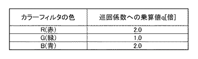
(8)カラーフィルタの分光特性
前述したように、撮像素子で用いられるカラーフィルタは、R、G、Bの3色の原色カラーフィルタを用いたベイヤー配列の周期構造をとっているのが一般的である。上述したR、G、Bの3色のカラーフィルタを備えた各々の画素から出力される画素信号のうち、人間の視覚特性として、G画素に対して非常に敏感であるのに対し、RB画素に対してはG画素ほどは敏感で無いという特徴がある。つまり、信号レベルの段差がG画素に対しては目立って見えるのに対し、RB画素は、G画素ほどは目立ち難い。例として、G画素は信号レベルの段差が±10LSBを超えたときに目立ち始めるが、RB画素については、±20LSBまでは目立たないといった、視覚的なレベル段差の見え方(限界値)の違いが生じる。
(8) Spectral Characteristics of Color Filter As described above, the color filters used in the image pickup device generally have a periodic structure of Bayer arrangement using three primary color filters of R, G and B. It is. Of the pixel signals output from each pixel provided with the R, G, and B color filters described above, it is very sensitive to G pixels as human visual characteristics, while RB pixels are very sensitive. Is characterized by being less sensitive than G pixels. That is, while the step of the signal level looks noticeable to the G pixel, the RB pixel is less noticeable to the G pixel. As an example, G pixels start to stand out when the signal level difference exceeds ± 10 LSB, but for RB pixels, they do not stand out to ± 20 LSB, so there is a difference in visual level difference (limit value) It occurs.
そこで、本実施形態においては、G画素を基準(1.0)として、R画素、B画素の巡回係数pに対して、乗算値qを乗算することで、RGB画素毎に異なる巡回係数を設定する。具体的には、G画素に対して、RB画素の乗算値qを1.0よりも大きくすることで、オフセット補正値βf(n)の変動が画像上に信号レベルの段差が見え始める限界値以下の状態を維持しつつ、かつ理想値への追従を早めることが可能となる。特に、電源起動時や撮像素子の駆動方法の切替え時などに急激にオフセット補正値β(n)が変化するが、急激な変化に対しては感度の低いRB画素でも、信号レベルの段差として見えてしまう。つまり、巡回係数を画像上に信号レベルの段差が見え始める限界値(±20LSB)以下に抑えつつ、理想値への追従速度はできるだけ早くしておくことがRB画素の巡回係数として好ましい。 Therefore, in the present embodiment, different cyclic coefficients are set for each RGB pixel by multiplying the cyclic coefficient p of the R pixel and the B pixel by the multiplication value q with the G pixel as the reference (1.0). Do. Specifically, by setting the multiplication value q of the RB pixel to be larger than 1.0 with respect to the G pixel, the limit value at which the variation of the offset correction value βf (n) starts to show the step of the signal level on the image It is possible to accelerate the follow-up to the ideal value while maintaining the following condition. In particular, the offset correction value β (n) changes rapidly at the time of power supply start-up or switching of the driving method of the imaging device, etc. However, even the RB pixel with low sensitivity to the rapid change looks as a step of the signal level It will That is, it is preferable as the cyclic coefficient of the RB pixel to keep the tracking speed to the ideal value as fast as possible while suppressing the cyclic coefficient to the limit value (± 20 LSB) at which the step of the signal level starts to be visible on the image.
図16は、カラーフィルタの各色に対する、巡回係数への乗算値qを示している。G画素が基準となるため、G画素の乗算値qは1.0倍としている。また、本実施形態では、R画素、B画素については、乗算値qを2.0倍としている。なお、本実施形態においては、RB画素の乗算値qを2.0倍としているが、巡回係数pと乗算値qとの乗算結果が1.0よりも大きくなった場合は、乗算結果を1.0とする。 FIG. 16 shows the multiplication value q to the cyclic coefficient for each color of the color filter. Since the G pixel is a reference, the multiplication value q of the G pixel is 1.0. Further, in the present embodiment, the multiplication value q is 2.0 for the R pixel and the B pixel. In this embodiment, although the multiplication value q of the RB pixel is 2.0 times, when the multiplication result of the cyclic coefficient p and the multiplication value q is larger than 1.0, the multiplication result is 1 .0.
こうすることで、オフセット補正値βf(n)の変動を、画像上に信号レベルの段差が見え始める限界値以下に抑えつつ、急激な理想値の変化に対しても、迅速にオフセット補正値βf(n)を追従させることができる。 By doing this, while suppressing the variation of the offset correction value βf (n) below the limit value at which the level difference of the signal level starts to be visible on the image, the offset correction value βf can be quickly also against sudden changes in the ideal value. (N) can be made to follow.
以上説明したように、R画素、G画素、B画素毎に異なる巡回係数を設定し、各々の画素に対して巡回係数を最適化する。これにより、各色の画素のオフセット補正値βf(n)の変動を、画像上に信号レベルの段差が見え始める限界値以下に抑えつつ、急激な理想値の変化に対しても迅速にオフセット補正値βf(n)を追従させることができる。 As described above, different cyclic coefficients are set for each of the R, G, and B pixels, and the cyclic coefficients are optimized for each pixel. As a result, while suppressing the variation of the offset correction value βf (n) of the pixels of each color below the limit value at which the step of the signal level starts to be visible on the image, the offset correction value can be quickly also against sudden changes in the ideal value. β f (n) can be made to follow.
(9)列アンプ群130のゲイン切替えに応じて判定レベルを変更した場合
低照度時において、画像信号のS/N比を改善するために、撮像素子1の列アンプ群130のゲインを切替えることがある。列アンプ群130のゲインを切替えることで、列アンプ群130以降の回路にて発生するノイズ成分を、画素信号に対して相対的に小さくすることが可能となり、S/N比を改善することができる。
(9) When the determination level is changed according to the gain switching of the column amplifier group 130: The gain of the
本実施形態においては、列アンプ群130のゲインは、アナログゲインを想定しており、離散的なゲイン設定を持つ。具体的には、2倍、4倍の設定を持ち、通常は2倍の設定となっており、低照度時には4倍の設定に切替える。
In the present embodiment, the gains of the
判定レベルVs近傍の信号レベルを有する画素信号が、列アンプ群130のゲイン設定の切替えにより増幅された場合、判定レベルVsをゲイン切替えによる増幅率に対応するように高いレベルに変更する必要がある。これは、万が一レベル段差が生じていた場合に、画面内における信号レベルの段差の発生位置が瞬時に変わってしまうからである。特に、列アンプ群130のゲインの切替え後において、信号レベルの段差が発生する画素が多い場合、画像として目立ってしまう。本実施形態では、列アンプ群130のゲイン切替えに応じて判定レベルVsを変更する際における、巡回係数の設定方法について説明する。
When a pixel signal having a signal level near the determination level Vs is amplified by switching the gain setting of the
本第1の実施形態では、列アンプ群130のゲイン切替え後に変更された判定レベルVsに応じて、巡回係数pに乗算するための乗算値qの設定値を変更する。図17は、列アンプ群130のゲイン切替え後の判定レベルVsに対する、巡回係数に乗算する乗算値qを示している。ここでは、AD変換のレンジが最大で12bit(0〜4095LSB)であって、乗算値qの基準値(×1.0)は、列アンプ群130のゲイン切替え後の判定レベルVsが、段差レベルが最も目立ち難い0〜511LSBの範囲であった場合とする。
In the first embodiment, the set value of the multiplication value q for multiplying the cyclic coefficient p is changed according to the determination level Vs changed after the gain switching of the
上記基準値に対し、列アンプ群130のゲイン切替え後の判定レベルVsが2048〜4095LSBの場合は乗算値q=4.0倍、判定レベルVsが512〜2047LSBの場合は乗算値q=2.0倍となるようにする。つまり、段差レベルが目立ち易くなるにつれて、巡回係数が高くなるように設定し、追従性を向上させる。なお、本実施形態においては、列アンプ切替え後の信号レベルが2048〜4095LSBの場合、乗算値qを4.0倍としているが、巡回係数pと乗算値qとの乗算結果が1.0よりも大きくなった場合は、乗算結果を1.0とする。
When the determination level Vs after gain switching of the
このようにすることで、列アンプ群130のゲイン切替え後の判定レベルVsが大きい場合、すなわちS信号の信号レベルの段差が目立ち易い場合は、巡回係数を一時的に高くすることでオフセット補正値βf(n)を迅速に理想値付近に収束させる。一方、列アンプ群130のゲイン切替え後の判定レベルVsが小さい場合、すなわちS信号の信号レベルの段差が目立ち難い場合は、巡回係数を低いまま維持することでオフセット補正値βf(n)の変動を低減させる。また、列アンプ群130のゲイン切替え直後のみ、この乗算値を適用しても良い。
By doing this, when the determination level Vs after gain switching of the
以上説明したように、列アンプ群130のゲイン切替えに応じて判定レベルを変更する際に、列アンプ群130のゲイン切替え後に設定した判定レベルVsの大きさに応じて、巡回係数の設定値を変更する。これにより、画像として段差が見え難い状態を維持しつつ、オフセット補正値βf(n)が理想値付近に収束するまでの時間と、ノイズによるオフセット補正値の変動の低減効果を、最適化させることができる。
As described above, when the determination level is changed according to the gain switching of the
以上、好適なフィルタリング処理方法について、いくつかの例を挙げて説明したが、これら複数を考慮して巡回係数を決定しても良い。また、本実施形態においては一つの例として巡回係数を示してきたが、各条件に対する巡回係数の設定方法としては必ずしもこの限りでなく、ノイズの発生条件や、温度変化率、撮像素子の駆動切り替えによる理想値の変化量などに応じて決定すると良い。 As mentioned above, although the suitable filtering processing method was mentioned taking several examples and demonstrated, you may determine a circulation coefficient in consideration of these plurality. In addition, although the cyclic coefficient is shown as one example in the present embodiment, the method of setting the cyclic coefficient for each condition is not necessarily limited to this, and noise generation conditions, temperature change rates, drive switching of the imaging device It is good to decide according to the amount of change of the ideal value by.
<第2の実施形態>
以下、本発明の第2の実施形態について説明する。第2の実施形態において用いられる撮像装置は、第1の実施形態で図1を参照して説明した撮像装置と同様の構成を有するため、説明は省略し、差異についてのみ説明する。
Second Embodiment
Hereinafter, a second embodiment of the present invention will be described. Since the imaging device used in the second embodiment has the same configuration as the imaging device described with reference to FIG. 1 in the first embodiment, the description will be omitted, and only differences will be described.
第2の実施形態では、図5に示す第1の実施形態の画素部110の構成に対して、図18に示すように、有効画素領域を水平方向に4分割している。画面左から順に、有効画素領域A、有効画素領域B、有効画素領域C、有効画素領域Dとする。また、有効画素領域に対応させて、ダミー画素領域も水平方向に4分割し、画面左から順に、ダミー画素領域A、ダミー画素領域B、ダミー画素領域C、ダミー画素領域Dとする。このように、水平方向に対していくつかの領域に分割することで、AD変換器の性能が水平方向にばらついた場合でも、より理想値に近い補正を行うことができる。
In the second embodiment, as shown in FIG. 18, the effective pixel area is divided into four in the horizontal direction with respect to the configuration of the
上述した第1の実施形態では、画面全体のダミー画素を用いて傾きの比αとオフセット量βを算出したが、本実施形態においては、分割されたA〜Dの領域毎に上記式(3)におけるα、βを算出する。上記領域ごとに算出されたオフセット補正値βfについては、上述した第1の実施形態と同様の処理を行うことで、信号レベルの段差が見えないようにする。 In the first embodiment described above, the inclination ratio α and the offset amount β are calculated using dummy pixels on the entire screen, but in the present embodiment, the above equation (3) is calculated for each of the divided areas A to D. Calculate α and β in). The offset correction value βf calculated for each of the regions is processed in the same manner as in the above-described first embodiment to make the level difference between signal levels invisible.
以上説明したように、水平方向に対して複数の領域に分割し、各々の領域についてオフセット補正値βf(n)を算出する。これにより、AD変換器の性能が水平方向にばらついた場合でも、より理想値に近い補正を行うことが可能となり、さらに、第1の実施形態と同様の効果を得ることができる。 As described above, the image is divided into a plurality of areas in the horizontal direction, and the offset correction value βf (n) is calculated for each area. Thus, even when the performance of the AD converter varies in the horizontal direction, it is possible to perform correction closer to the ideal value, and it is possible to obtain the same effect as that of the first embodiment.
なお、第1及び第2の実施形態では、異なる傾きの2種類のランプ信号について記載したが、3種類以上の傾きについても同様の扱いができるため、ランプ信号の種類の数により本願発明が制限されるものではない。また、ダミー画素領域を用いて算出された補正値に対してフィルタリング処理を行うことが必須であり、補正値の取得方法及び演算方法などは、第1の実施形態に記載したものが代表的なものであるが、これに限られるものではない。 In the first and second embodiments, two types of ramp signals having different slopes are described, but the present invention is limited by the number of types of ramp signals because three or more types of slopes can be treated in the same manner. It is not something to be done. In addition, it is essential to perform the filtering process on the correction value calculated using the dummy pixel area, and the method of obtaining the correction value, the calculation method, and the like are the ones described in the first embodiment. Although it is a thing, it is not restricted to this.
また、本第1及び第2の実施形態においては、撮像素子1として、回路規模の小さい列ADCを列毎に1つ備えた構成をとっているが、本発明はこれに限られるものではない。例えば、各列に複数の列ADCを備え、それぞれが異なるスロープのランプ信号を用いてAD変換し、いずれかを選択する構成や、特開2013−009087号公報に記載されている構成を有するものであってもよい。特開2013−009087号公報には、撮像素子内にある列アンプ回路において、画素信号のレベルに応じて画素毎に、第1のランプ信号と、第1のランプ信号よりも傾きが小さい第2のランプ信号のいずれかを選択的に用いてAD変換を行うことが開示されている。即ち、異なる傾きを有する複数のランプ信号のいずれかによりAD変換された画素信号を選択的に用いて各フレームの画像を構成するものであれば、本発明を適用することが可能である。
In the first and second embodiments, the
1:撮像素子、2:画像処理部、100:タイミング制御部、110:画素部、120:垂直走査回路、130:列アンプ群、140:ランプ回路、150:列アナログデジタル変換器群(列ADC群)、151:比較部、152:カウンタ・ラッチ回路、160:水平転送回路、170:信号処理回路、180:外部出力回路、400:定電圧回路 1: Imaging device 2: Image processing unit 100: Timing control unit 110: Pixel unit 120: Vertical scanning circuit 130: Column amplifier group 140: Lamp circuit 150: Column analog-to-digital converter group (column ADC Groups: 151: Comparison unit, 152: Counter-latch circuit, 160: Horizontal transfer circuit, 170: Signal processing circuit, 180: External output circuit, 400: Constant voltage circuit
Claims (20)
互いに異なる傾きを有する複数の参照信号を用いてアナログ信号をデジタル信号に変換するアナログデジタル変換手段と、
予め決められた複数の異なる出力レベルのアナログ信号を前記アナログデジタル変換手段に供給する電圧供給手段と、
前記電圧供給手段により供給される前記複数の異なる出力レベルのアナログ信号を前記アナログデジタル変換手段により前記複数の参照信号を用いてそれぞれ変換して得られた複数のデジタル信号に基づいて、前記複数の参照信号を用いて前記画素部から出力されるアナログ信号を前記アナログデジタル変換手段により変換して得られるデジタル信号の傾き及びオフセットを補正するための補正値を算出する算出手段と、を有し、
前記算出手段は、前記オフセットを補正するためのオフセット補正値を巡回係数により重み付け加算するフィルタリング処理を行い、新たに取得したフィルタリング処理前のオフセット補正値と、前のフレームにおけるフィルタリング処理後のオフセット補正値との差分が閾値よりも大きい場合に、前記巡回係数を0に設定することを特徴とする撮像装置。 A pixel unit in which a plurality of pixels are two-dimensionally arranged;
Analog-to-digital conversion means for converting an analog signal into a digital signal using a plurality of reference signals having different inclinations from each other;
Voltage supply means for supplying analog signals of a plurality of predetermined different output levels to the analog-to-digital conversion means;
Based on the plurality of digital signals obtained by converting each using the plurality of reference signals by an analog signal of the plurality of different power levels the analog-digital converter means supplied by said voltage supply means, said plurality of Calculating means for calculating a correction value for correcting an inclination and an offset of a digital signal obtained by converting the analog signal output from the pixel unit by the analog-to-digital converter using a reference signal ;
The calculation means performs filtering processing in which the offset correction value for correcting the offset is weighted and added by a cyclic coefficient, and the newly obtained offset correction value before filtering processing and the offset correction after filtering processing in the previous frame An imaging apparatus , wherein the cyclic coefficient is set to 0 when a difference from a value is larger than a threshold .
βf(n)=β(n)×p+βf(n−1)×(1−p),(0≦p≦1)
によりフィルタリング処理後のオフセット補正値βf(n)を求めることを特徴とする請求項1または2に記載の撮像装置。 When the offset correction value before the filtering process is β (n) , the offset correction value after the filtering process in the previous frame is βf (n−1), and the cyclic coefficient is p.
β f (n) = β (n) × p + β f (n-1) × (1- p), (0 p p 1 1)
3. The image pickup apparatus according to claim 1, wherein the offset correction value βf (n) after the filtering process is obtained by
前記温度検出手段により測定された温度の変化率の絶対値が予め決められた範囲内にある場合に、該範囲より小さい場合よりも、大きい値を前記巡回係数に設定することを特徴とする請求項1乃至3のいずれか1項に記載の撮像装置。 Further comprising temperature detection means for measuring the temperature;
When the absolute value of the rate of change of temperature measured by the temperature detecting means is within a predetermined range, a larger value is set as the cyclic coefficient than when it is smaller than the range. Item 4. The imaging device according to any one of Items 1 to 3 .
前記映像出力として用いるフレームで算出された前記オフセット補正値と、前記映像出力として用いないフレームで算出された前記オフセット補正値との差分の絶対値が予め決められた範囲内にある場合に、該範囲より大きい場合よりも、より大きい値を前記巡回係数に乗ずることを特徴とする請求項1乃至7のいずれか1項に記載の撮像装置。 An image obtained by reading a front Kiga Motobu, and a frame with and without frame used as a video output,
When the absolute value of the difference between the offset correction value calculated in the frame used as the video output and the offset correction value calculated in the frame not used as the video output is within a predetermined range The imaging apparatus according to any one of claims 1 to 7 , wherein the cyclic coefficient is multiplied by a larger value than when larger than the range.
前記動き量の検出手段により検出された動き量が予め決められた範囲内にある場合に、該範囲より小さい場合よりも、大きい値を前記巡回係数に乗ずることを特徴とする請求項1乃至8のいずれか1項に記載の撮像装置。 The apparatus further comprises motion amount detection means for detecting the motion amount of the subject,
If within a range that the amount of motion detected by the detecting means of the movement amount is predetermined, according to claim 1 to 8 than smaller than said range, characterized by multiplying the larger value to the cyclic coefficient The imaging device according to any one of the above.
赤または青のフィルタにより覆われた画素に対応するデジタル信号を補正するための補正値は、緑のフィルタにより覆われた画素に対応するデジタル信号を補正するための補正値よりも大きい値を前記巡回係数に乗じて算出することを特徴とする請求項1乃至9のいずれか1項に記載の撮像装置。 Before outs Motobu is covered by primary color filters of the Bayer array,
The correction value for correcting the digital signal corresponding to the pixel covered by the red or blue filter is larger than the correction value for correcting the digital signal corresponding to the pixel covered by the green filter. The imaging apparatus according to any one of claims 1 to 9 , wherein the imaging apparatus is calculated by multiplying a cyclic coefficient.
前記アナログデジタル変換手段は、前記画素部を構成する各画素から出力されるアナログ信号の出力レベルを予め決められた判定レベルと比較し、
前記増幅手段による増幅率が変化した場合に、前記判定レベルを前記増幅率の変化に対応するように変更した値が予め決められた範囲内にある場合に、該範囲より小さい場合よりも、大きい値を前記巡回係数に乗ずることを特徴とする請求項1乃至10のいずれか1項に記載の撮像装置。 The analog signal output from each pixel constituting the front Kiga Motobu, further comprising amplifying means for amplifying before conversion by the analog-digital converting means,
The analog-to-digital converting means compares the predetermined judgment level output level of the analog signal output from each pixel constituting the front Kiga Motobu,
When the amplification factor by the amplification means changes, the value obtained by changing the determination level to correspond to the change in amplification factor is larger than that in the case where it is smaller than the predetermined range. The imaging apparatus according to any one of claims 1 to 10 , wherein the value is multiplied by the cyclic coefficient.
電圧供給手段が、予め決められた複数の異なる出力レベルのアナログ信号をアナログデジタル変換手段に供給する電圧供給工程と、
前記アナログデジタル変換手段が、前記電圧供給工程で供給される前記複数の異なる出力レベルのアナログ信号を、互いに異なる傾きを有する複数の参照信号を用いて複数のデジタル信号に変換するアナログデジタル変換工程と、
算出手段が、前記アナログデジタル変換工程で変換された前記複数のデジタル信号に基づいて、前記複数の異なる傾きの比とオフセット量とを算出し、前記傾きの比とオフセット量とに基づいて、前記複数の参照信号を用いて前記画素部から出力されるアナログ信号を前記アナログデジタル変換手段により変換して得られるデジタル信号の傾き及びオフセットを補正するための補正値を算出する算出工程と、を有し、
前記算出工程では、前記オフセットを補正するためのオフセット補正値を巡回係数により重み付け加算するフィルタリング処理を行い、新たに取得したフィルタリング処理前のオフセット補正値と、前のフレームにおけるフィルタリング処理後のオフセット補正値との差分が閾値よりも大きい場合に、前記巡回係数を0に設定することを特徴とする撮像装置の制御方法。 A control method of an imaging device having a pixel unit in which a plurality of pixels are two-dimensionally arranged,
Voltage supplying means for supplying analog signals of a plurality of different output levels determined in advance to the analog to digital conversion means;
An analog-to-digital conversion step of converting the plurality of different output level analog signals supplied in the voltage supply step into a plurality of digital signals using a plurality of reference signals having different inclinations; ,
Calculating means, on the basis of the analog plurality of digital signal converted by the digital conversion process, and calculates the ratio and the offset amount of the plurality of different slopes, on the basis of the ratio and the offset amount of the tilt, the Calculating a correction value for correcting an inclination and an offset of a digital signal obtained by converting the analog signal output from the pixel unit using the plurality of reference signals by the analog-to-digital converter; And
In the calculation step, filtering processing is performed in which the offset correction value for correcting the offset is weighted and added by a cyclic coefficient, and the newly obtained offset correction value before filtering processing and the offset correction after filtering processing in the previous frame The control method of an imaging apparatus , wherein the cyclic coefficient is set to 0 when a difference from a value is larger than a threshold .
Priority Applications (3)
| Application Number | Priority Date | Filing Date | Title |
|---|---|---|---|
| JP2015010676A JP6525602B2 (en) | 2015-01-22 | 2015-01-22 | Image pickup apparatus and control method thereof |
| US15/001,944 US9736406B2 (en) | 2015-01-22 | 2016-01-20 | Image capturing apparatus and control method thereof |
| CN201610044460.3A CN105828003B (en) | 2015-01-22 | 2016-01-22 | The control method of picture pick-up device and picture pick-up device |
Applications Claiming Priority (1)
| Application Number | Priority Date | Filing Date | Title |
|---|---|---|---|
| JP2015010676A JP6525602B2 (en) | 2015-01-22 | 2015-01-22 | Image pickup apparatus and control method thereof |
Publications (3)
| Publication Number | Publication Date |
|---|---|
| JP2016134908A JP2016134908A (en) | 2016-07-25 |
| JP2016134908A5 JP2016134908A5 (en) | 2018-03-01 |
| JP6525602B2 true JP6525602B2 (en) | 2019-06-05 |
Family
ID=56434711
Family Applications (1)
| Application Number | Title | Priority Date | Filing Date |
|---|---|---|---|
| JP2015010676A Active JP6525602B2 (en) | 2015-01-22 | 2015-01-22 | Image pickup apparatus and control method thereof |
Country Status (1)
| Country | Link |
|---|---|
| JP (1) | JP6525602B2 (en) |
Families Citing this family (3)
| Publication number | Priority date | Publication date | Assignee | Title |
|---|---|---|---|---|
| JP6530736B2 (en) * | 2016-10-18 | 2019-06-12 | キヤノン株式会社 | Image pickup apparatus and control method thereof |
| CN115712118B (en) * | 2022-11-07 | 2023-08-11 | 江苏省水利科学研究院 | Pixel offset tracking monitoring and correcting method |
| CN115883977B (en) * | 2023-03-03 | 2023-04-28 | 合肥埃科光电科技股份有限公司 | Image sensor data smear real-time correction method, device and storage medium |
Family Cites Families (6)
| Publication number | Priority date | Publication date | Assignee | Title |
|---|---|---|---|---|
| JP4328115B2 (en) * | 2003-03-24 | 2009-09-09 | パナソニック株式会社 | Solid-state imaging device |
| JP2007208832A (en) * | 2006-02-03 | 2007-08-16 | Fujifilm Corp | Digital camera |
| JP5792990B2 (en) * | 2011-04-28 | 2015-10-14 | キヤノン株式会社 | Image processing apparatus and control method thereof |
| JP6017279B2 (en) * | 2012-11-22 | 2016-10-26 | オリンパス株式会社 | Image processing apparatus, image processing method, and program |
| JP2014212450A (en) * | 2013-04-18 | 2014-11-13 | キヤノン株式会社 | Imaging device |
| JP6226551B2 (en) * | 2013-05-08 | 2017-11-08 | キヤノン株式会社 | Imaging device |
-
2015
- 2015-01-22 JP JP2015010676A patent/JP6525602B2/en active Active
Also Published As
| Publication number | Publication date |
|---|---|
| JP2016134908A (en) | 2016-07-25 |
Similar Documents
| Publication | Publication Date | Title |
|---|---|---|
| US9736406B2 (en) | Image capturing apparatus and control method thereof | |
| JP4364903B2 (en) | Automatic gain control circuit | |
| JP5350466B2 (en) | Column fixed pattern noise correction method | |
| CN107154801B (en) | Signal processing apparatus and method, image pickup apparatus, and control apparatus and method | |
| US20120273655A1 (en) | Image sensing apparatus and control method thereof | |
| CN107154803B (en) | Signal processing apparatus, signal processing method, and image pickup apparatus | |
| US8982250B2 (en) | Image processing apparatus | |
| US11184565B2 (en) | Image pickup apparatus and its control method | |
| US10863101B2 (en) | Image capturing apparatus and method of controlling the same | |
| JP6494301B2 (en) | Imaging apparatus and control method thereof | |
| US20200288052A1 (en) | Image capturing device for auto exposure | |
| JP6525602B2 (en) | Image pickup apparatus and control method thereof | |
| JP5520833B2 (en) | Imaging method and imaging apparatus | |
| US10313617B2 (en) | Image capturing apparatus, control method for the same, and storage medium | |
| JP6433276B2 (en) | Imaging apparatus, control method therefor, program, and storage medium | |
| JP5588729B2 (en) | Image signal processing device | |
| US11284017B2 (en) | Image pickup device and storage medium | |
| US8885072B2 (en) | Solid-state imaging device, imaging method, and camera module | |
| JP2017152838A (en) | Imaging apparatus and control method for imaging apparatus | |
| US20230412940A1 (en) | Image pickup apparatus and image processing method | |
| US20230386000A1 (en) | Image processing apparatus, control method thereof, and non-transitory computer-readable storage medium | |
| KR100858073B1 (en) | Automatic gain control circuit | |
| JP2004336242A (en) | Correction apparatus | |
| JP2021153291A (en) | Imaging apparatus, computer program, and storage medium | |
| JP2004357238A (en) | Image pickup device and its image processing method |
Legal Events
| Date | Code | Title | Description |
|---|---|---|---|
| A521 | Request for written amendment filed |
Free format text: JAPANESE INTERMEDIATE CODE: A523 Effective date: 20180117 |
|
| A621 | Written request for application examination |
Free format text: JAPANESE INTERMEDIATE CODE: A621 Effective date: 20180117 |
|
| A977 | Report on retrieval |
Free format text: JAPANESE INTERMEDIATE CODE: A971007 Effective date: 20181102 |
|
| A131 | Notification of reasons for refusal |
Free format text: JAPANESE INTERMEDIATE CODE: A131 Effective date: 20181116 |
|
| A521 | Request for written amendment filed |
Free format text: JAPANESE INTERMEDIATE CODE: A523 Effective date: 20190109 |
|
| TRDD | Decision of grant or rejection written | ||
| A01 | Written decision to grant a patent or to grant a registration (utility model) |
Free format text: JAPANESE INTERMEDIATE CODE: A01 Effective date: 20190408 |
|
| A61 | First payment of annual fees (during grant procedure) |
Free format text: JAPANESE INTERMEDIATE CODE: A61 Effective date: 20190507 |
|
| R151 | Written notification of patent or utility model registration |
Ref document number: 6525602 Country of ref document: JP Free format text: JAPANESE INTERMEDIATE CODE: R151 |