JP6642484B2 - Semiconductor device and method of manufacturing the same - Google Patents
Semiconductor device and method of manufacturing the same Download PDFInfo
- Publication number
- JP6642484B2 JP6642484B2 JP2017037277A JP2017037277A JP6642484B2 JP 6642484 B2 JP6642484 B2 JP 6642484B2 JP 2017037277 A JP2017037277 A JP 2017037277A JP 2017037277 A JP2017037277 A JP 2017037277A JP 6642484 B2 JP6642484 B2 JP 6642484B2
- Authority
- JP
- Japan
- Prior art keywords
- molded body
- primary molded
- insertion hole
- semiconductor device
- housing component
- Prior art date
- Legal status (The legal status is an assumption and is not a legal conclusion. Google has not performed a legal analysis and makes no representation as to the accuracy of the status listed.)
- Expired - Fee Related
Links
- 239000004065 semiconductor Substances 0.000 title claims description 176
- 238000004519 manufacturing process Methods 0.000 title claims description 24
- 238000003780 insertion Methods 0.000 claims description 198
- 230000037431 insertion Effects 0.000 claims description 198
- 229920005989 resin Polymers 0.000 claims description 175
- 239000011347 resin Substances 0.000 claims description 175
- 238000000465 moulding Methods 0.000 claims description 140
- 239000000463 material Substances 0.000 claims description 53
- 238000001514 detection method Methods 0.000 claims description 20
- 230000001681 protective effect Effects 0.000 claims description 19
- 238000003825 pressing Methods 0.000 claims description 13
- 238000007789 sealing Methods 0.000 claims description 6
- 229920005992 thermoplastic resin Polymers 0.000 description 8
- 230000007547 defect Effects 0.000 description 7
- 238000000034 method Methods 0.000 description 7
- 239000003566 sealing material Substances 0.000 description 7
- 230000001629 suppression Effects 0.000 description 7
- 239000000654 additive Substances 0.000 description 6
- 229920001187 thermosetting polymer Polymers 0.000 description 6
- 239000004734 Polyphenylene sulfide Substances 0.000 description 5
- 230000000996 additive effect Effects 0.000 description 5
- 238000005259 measurement Methods 0.000 description 5
- 229920000069 polyphenylene sulfide Polymers 0.000 description 5
- 125000000524 functional group Chemical group 0.000 description 4
- 238000005304 joining Methods 0.000 description 4
- 239000000945 filler Substances 0.000 description 3
- 239000000446 fuel Substances 0.000 description 3
- 239000011810 insulating material Substances 0.000 description 3
- 239000002184 metal Substances 0.000 description 3
- 239000007769 metal material Substances 0.000 description 3
- 230000002093 peripheral effect Effects 0.000 description 3
- 238000001721 transfer moulding Methods 0.000 description 3
- VYPSYNLAJGMNEJ-UHFFFAOYSA-N Silicium dioxide Chemical compound O=[Si]=O VYPSYNLAJGMNEJ-UHFFFAOYSA-N 0.000 description 2
- 238000010521 absorption reaction Methods 0.000 description 2
- 239000000853 adhesive Substances 0.000 description 2
- 230000001070 adhesive effect Effects 0.000 description 2
- 230000015572 biosynthetic process Effects 0.000 description 2
- 238000000748 compression moulding Methods 0.000 description 2
- 238000010586 diagram Methods 0.000 description 2
- 239000013013 elastic material Substances 0.000 description 2
- 239000003822 epoxy resin Substances 0.000 description 2
- 238000010438 heat treatment Methods 0.000 description 2
- 229920001707 polybutylene terephthalate Polymers 0.000 description 2
- 229920000647 polyepoxide Polymers 0.000 description 2
- 230000035882 stress Effects 0.000 description 2
- 239000000758 substrate Substances 0.000 description 2
- PNEYBMLMFCGWSK-UHFFFAOYSA-N aluminium oxide Inorganic materials [O-2].[O-2].[O-2].[Al+3].[Al+3] PNEYBMLMFCGWSK-UHFFFAOYSA-N 0.000 description 1
- 238000002485 combustion reaction Methods 0.000 description 1
- 239000004020 conductor Substances 0.000 description 1
- 230000000994 depressogenic effect Effects 0.000 description 1
- 238000006073 displacement reaction Methods 0.000 description 1
- 230000000694 effects Effects 0.000 description 1
- 230000001747 exhibiting effect Effects 0.000 description 1
- 239000011796 hollow space material Substances 0.000 description 1
- 238000002347 injection Methods 0.000 description 1
- 239000007924 injection Substances 0.000 description 1
- 238000001746 injection moulding Methods 0.000 description 1
- 230000005389 magnetism Effects 0.000 description 1
- -1 polybutylene terephthalate Polymers 0.000 description 1
- 238000012545 processing Methods 0.000 description 1
- 239000000377 silicon dioxide Substances 0.000 description 1
- 238000009751 slip forming Methods 0.000 description 1
- 230000008646 thermal stress Effects 0.000 description 1
Images


Classifications
-
- B—PERFORMING OPERATIONS; TRANSPORTING
- B29—WORKING OF PLASTICS; WORKING OF SUBSTANCES IN A PLASTIC STATE IN GENERAL
- B29C—SHAPING OR JOINING OF PLASTICS; SHAPING OF MATERIAL IN A PLASTIC STATE, NOT OTHERWISE PROVIDED FOR; AFTER-TREATMENT OF THE SHAPED PRODUCTS, e.g. REPAIRING
- B29C33/00—Moulds or cores; Details thereof or accessories therefor
- B29C33/12—Moulds or cores; Details thereof or accessories therefor with incorporated means for positioning inserts, e.g. labels
-
- G—PHYSICS
- G01—MEASURING; TESTING
- G01L—MEASURING FORCE, STRESS, TORQUE, WORK, MECHANICAL POWER, MECHANICAL EFFICIENCY, OR FLUID PRESSURE
- G01L19/00—Details of, or accessories for, apparatus for measuring steady or quasi-steady pressure of a fluent medium insofar as such details or accessories are not special to particular types of pressure gauges
- G01L19/14—Housings
- G01L19/142—Multiple part housings
- G01L19/143—Two part housings
-
- B—PERFORMING OPERATIONS; TRANSPORTING
- B29—WORKING OF PLASTICS; WORKING OF SUBSTANCES IN A PLASTIC STATE IN GENERAL
- B29C—SHAPING OR JOINING OF PLASTICS; SHAPING OF MATERIAL IN A PLASTIC STATE, NOT OTHERWISE PROVIDED FOR; AFTER-TREATMENT OF THE SHAPED PRODUCTS, e.g. REPAIRING
- B29C45/00—Injection moulding, i.e. forcing the required volume of moulding material through a nozzle into a closed mould; Apparatus therefor
- B29C45/16—Making multilayered or multicoloured articles
- B29C45/1671—Making multilayered or multicoloured articles with an insert
-
- G—PHYSICS
- G01—MEASURING; TESTING
- G01L—MEASURING FORCE, STRESS, TORQUE, WORK, MECHANICAL POWER, MECHANICAL EFFICIENCY, OR FLUID PRESSURE
- G01L19/00—Details of, or accessories for, apparatus for measuring steady or quasi-steady pressure of a fluent medium insofar as such details or accessories are not special to particular types of pressure gauges
- G01L19/14—Housings
- G01L19/142—Multiple part housings
-
- G—PHYSICS
- G01—MEASURING; TESTING
- G01L—MEASURING FORCE, STRESS, TORQUE, WORK, MECHANICAL POWER, MECHANICAL EFFICIENCY, OR FLUID PRESSURE
- G01L19/00—Details of, or accessories for, apparatus for measuring steady or quasi-steady pressure of a fluent medium insofar as such details or accessories are not special to particular types of pressure gauges
- G01L19/14—Housings
- G01L19/145—Housings with stress relieving means
-
- H—ELECTRICITY
- H01—ELECTRIC ELEMENTS
- H01L—SEMICONDUCTOR DEVICES NOT COVERED BY CLASS H10
- H01L21/00—Processes or apparatus adapted for the manufacture or treatment of semiconductor or solid state devices or of parts thereof
- H01L21/02—Manufacture or treatment of semiconductor devices or of parts thereof
- H01L21/04—Manufacture or treatment of semiconductor devices or of parts thereof the devices having potential barriers, e.g. a PN junction, depletion layer or carrier concentration layer
- H01L21/50—Assembly of semiconductor devices using processes or apparatus not provided for in a single one of the subgroups H01L21/06 - H01L21/326, e.g. sealing of a cap to a base of a container
- H01L21/56—Encapsulations, e.g. encapsulation layers, coatings
-
- H—ELECTRICITY
- H01—ELECTRIC ELEMENTS
- H01L—SEMICONDUCTOR DEVICES NOT COVERED BY CLASS H10
- H01L23/00—Details of semiconductor or other solid state devices
- H01L23/28—Encapsulations, e.g. encapsulating layers, coatings, e.g. for protection
- H01L23/31—Encapsulations, e.g. encapsulating layers, coatings, e.g. for protection characterised by the arrangement or shape
-
- B—PERFORMING OPERATIONS; TRANSPORTING
- B29—WORKING OF PLASTICS; WORKING OF SUBSTANCES IN A PLASTIC STATE IN GENERAL
- B29C—SHAPING OR JOINING OF PLASTICS; SHAPING OF MATERIAL IN A PLASTIC STATE, NOT OTHERWISE PROVIDED FOR; AFTER-TREATMENT OF THE SHAPED PRODUCTS, e.g. REPAIRING
- B29C45/00—Injection moulding, i.e. forcing the required volume of moulding material through a nozzle into a closed mould; Apparatus therefor
- B29C45/16—Making multilayered or multicoloured articles
- B29C2045/1682—Making multilayered or multicoloured articles preventing defects
-
- B—PERFORMING OPERATIONS; TRANSPORTING
- B29—WORKING OF PLASTICS; WORKING OF SUBSTANCES IN A PLASTIC STATE IN GENERAL
- B29C—SHAPING OR JOINING OF PLASTICS; SHAPING OF MATERIAL IN A PLASTIC STATE, NOT OTHERWISE PROVIDED FOR; AFTER-TREATMENT OF THE SHAPED PRODUCTS, e.g. REPAIRING
- B29C45/00—Injection moulding, i.e. forcing the required volume of moulding material through a nozzle into a closed mould; Apparatus therefor
- B29C45/14—Injection moulding, i.e. forcing the required volume of moulding material through a nozzle into a closed mould; Apparatus therefor incorporating preformed parts or layers, e.g. injection moulding around inserts or for coating articles
- B29C45/14065—Positioning or centering articles in the mould
-
- B—PERFORMING OPERATIONS; TRANSPORTING
- B29—WORKING OF PLASTICS; WORKING OF SUBSTANCES IN A PLASTIC STATE IN GENERAL
- B29C—SHAPING OR JOINING OF PLASTICS; SHAPING OF MATERIAL IN A PLASTIC STATE, NOT OTHERWISE PROVIDED FOR; AFTER-TREATMENT OF THE SHAPED PRODUCTS, e.g. REPAIRING
- B29C45/00—Injection moulding, i.e. forcing the required volume of moulding material through a nozzle into a closed mould; Apparatus therefor
- B29C45/14—Injection moulding, i.e. forcing the required volume of moulding material through a nozzle into a closed mould; Apparatus therefor incorporating preformed parts or layers, e.g. injection moulding around inserts or for coating articles
- B29C45/14336—Coating a portion of the article, e.g. the edge of the article
- B29C45/14418—Sealing means between mould and article
-
- B—PERFORMING OPERATIONS; TRANSPORTING
- B29—WORKING OF PLASTICS; WORKING OF SUBSTANCES IN A PLASTIC STATE IN GENERAL
- B29C—SHAPING OR JOINING OF PLASTICS; SHAPING OF MATERIAL IN A PLASTIC STATE, NOT OTHERWISE PROVIDED FOR; AFTER-TREATMENT OF THE SHAPED PRODUCTS, e.g. REPAIRING
- B29C45/00—Injection moulding, i.e. forcing the required volume of moulding material through a nozzle into a closed mould; Apparatus therefor
- B29C45/14—Injection moulding, i.e. forcing the required volume of moulding material through a nozzle into a closed mould; Apparatus therefor incorporating preformed parts or layers, e.g. injection moulding around inserts or for coating articles
- B29C45/14639—Injection moulding, i.e. forcing the required volume of moulding material through a nozzle into a closed mould; Apparatus therefor incorporating preformed parts or layers, e.g. injection moulding around inserts or for coating articles for obtaining an insulating effect, e.g. for electrical components
- B29C45/14655—Injection moulding, i.e. forcing the required volume of moulding material through a nozzle into a closed mould; Apparatus therefor incorporating preformed parts or layers, e.g. injection moulding around inserts or for coating articles for obtaining an insulating effect, e.g. for electrical components connected to or mounted on a carrier, e.g. lead frame
-
- B—PERFORMING OPERATIONS; TRANSPORTING
- B29—WORKING OF PLASTICS; WORKING OF SUBSTANCES IN A PLASTIC STATE IN GENERAL
- B29C—SHAPING OR JOINING OF PLASTICS; SHAPING OF MATERIAL IN A PLASTIC STATE, NOT OTHERWISE PROVIDED FOR; AFTER-TREATMENT OF THE SHAPED PRODUCTS, e.g. REPAIRING
- B29C45/00—Injection moulding, i.e. forcing the required volume of moulding material through a nozzle into a closed mould; Apparatus therefor
- B29C45/14—Injection moulding, i.e. forcing the required volume of moulding material through a nozzle into a closed mould; Apparatus therefor incorporating preformed parts or layers, e.g. injection moulding around inserts or for coating articles
- B29C45/14836—Preventing damage of inserts during injection, e.g. collapse of hollow inserts, breakage
-
- B—PERFORMING OPERATIONS; TRANSPORTING
- B29—WORKING OF PLASTICS; WORKING OF SUBSTANCES IN A PLASTIC STATE IN GENERAL
- B29K—INDEXING SCHEME ASSOCIATED WITH SUBCLASSES B29B, B29C OR B29D, RELATING TO MOULDING MATERIALS OR TO MATERIALS FOR MOULDS, REINFORCEMENTS, FILLERS OR PREFORMED PARTS, e.g. INSERTS
- B29K2995/00—Properties of moulding materials, reinforcements, fillers, preformed parts or moulds
- B29K2995/0012—Properties of moulding materials, reinforcements, fillers, preformed parts or moulds having particular thermal properties
-
- H—ELECTRICITY
- H01—ELECTRIC ELEMENTS
- H01L—SEMICONDUCTOR DEVICES NOT COVERED BY CLASS H10
- H01L23/00—Details of semiconductor or other solid state devices
- H01L23/28—Encapsulations, e.g. encapsulating layers, coatings, e.g. for protection
- H01L23/31—Encapsulations, e.g. encapsulating layers, coatings, e.g. for protection characterised by the arrangement or shape
- H01L23/3157—Partial encapsulation or coating
- H01L23/3185—Partial encapsulation or coating the coating covering also the sidewalls of the semiconductor body
-
- H—ELECTRICITY
- H01—ELECTRIC ELEMENTS
- H01L—SEMICONDUCTOR DEVICES NOT COVERED BY CLASS H10
- H01L2924/00—Indexing scheme for arrangements or methods for connecting or disconnecting semiconductor or solid-state bodies as covered by H01L24/00
- H01L2924/15—Details of package parts other than the semiconductor or other solid state devices to be connected
- H01L2924/181—Encapsulation
Landscapes
- Engineering & Computer Science (AREA)
- Physics & Mathematics (AREA)
- General Physics & Mathematics (AREA)
- Manufacturing & Machinery (AREA)
- Mechanical Engineering (AREA)
- Computer Hardware Design (AREA)
- Condensed Matter Physics & Semiconductors (AREA)
- Microelectronics & Electronic Packaging (AREA)
- Power Engineering (AREA)
- Child & Adolescent Psychology (AREA)
- Health & Medical Sciences (AREA)
- Structures Or Materials For Encapsulating Or Coating Semiconductor Devices Or Solid State Devices (AREA)
- Encapsulation Of And Coatings For Semiconductor Or Solid State Devices (AREA)
- Moulds For Moulding Plastics Or The Like (AREA)
- Casting Or Compression Moulding Of Plastics Or The Like (AREA)
- Measuring Fluid Pressure (AREA)
- Injection Moulding Of Plastics Or The Like (AREA)
Description
本発明は、二次成形体を備える半導体装置およびその製造方法に関する。 The present invention relates to a semiconductor device having a secondary molded body and a method for manufacturing the same.
従来より、物理量を検出する検出部を有する半導体チップを備える一次成形体と、一次成形体のうち検出部と異なる部分を覆う二次成形樹脂と、二次成形樹脂に取り付けられる筐体部品とを有してなる半導体装置が知られている。このような構成において、一次成形体は、半導体チップと、半導体チップのうち検出部と異なる領域を覆う一次成形樹脂とを有してなる。このような半導体装置およびその製造方法としては、例えば特許文献1に記載のものが知られている。
Conventionally, a primary molded body including a semiconductor chip having a detection unit for detecting a physical quantity, a secondary molding resin covering a portion of the primary molded body different from the detection unit, and a housing component attached to the
特許文献1に記載の半導体装置は、圧力を検出する検出部を有する半導体チップと熱硬化性樹脂によりなる一次成形樹脂とを備える一次成形体と、一次成形体のうち半導体チップと異なる領域を覆う二次成形樹脂と、フランジ形状の筐体部品とを備える。そして、筐体部品は、半導体チップを覆うためのドーム状の収容空間と当該空間に繋がる中空部が形成され、二次成形樹脂から露出した半導体チップが収容空間を形成した部分に覆われるように一次成形体および二次成形樹脂とシール材を介して接合されている。なお、フランジ形状の筐体部品は、収容空間が形成された部分の径が、中空部が形成された部分の径よりも大きいものとされている。 The semiconductor device described in Patent Literature 1 covers a primary molded body including a semiconductor chip having a detecting unit for detecting pressure and a primary molded resin made of a thermosetting resin, and covers a region of the primary molded body different from the semiconductor chip. A secondary molding resin and a flange-shaped housing component are provided. Then, the housing component is formed such that a dome-shaped housing space for covering the semiconductor chip and a hollow portion connected to the space are formed, and the semiconductor chip exposed from the secondary molding resin is covered by a portion forming the housing space. It is joined to the primary molding and the secondary molding resin via a sealing material. In the flange-shaped housing component, the diameter of the portion where the housing space is formed is larger than the diameter of the portion where the hollow portion is formed.
特許文献1に記載の半導体装置は、一次成形体を上型、下型およびスライド型によりなる金型のうち下型に固定した後、インサート成形により熱可塑性樹脂材料を流し込んで硬化させることで、一次成形体の一部を覆う二次成形樹脂を成形する工程を含む。この工程により、一次成形体のうち半導体チップが二次成形樹脂から露出すると共に、一次成形樹脂と二次成形樹脂との間に筐体部品と接合するためのシール材の充填に用いられる環状の溝が形成された二次成形体が得られる。そして、この二次成形体の溝にシール材を充填した後、当該シール材を介して二次成形体と上記の筐体部品とを接合することで、上記のような半導体装置を製造することができる。 The semiconductor device described in Patent Document 1 fixes the primary molded body to the lower mold of the upper mold, the lower mold and the slide mold, and then pours and hardens the thermoplastic resin material by insert molding. The method includes a step of molding a secondary molding resin covering a part of the primary molded body. By this step, the semiconductor chip of the primary molded body is exposed from the secondary molding resin, and an annular ring used for filling a sealing material between the primary molding resin and the secondary molding resin for joining with a housing component. A secondary formed body in which a groove is formed is obtained. Then, after filling the groove of the secondary molded body with the sealing material, the semiconductor device as described above is manufactured by joining the secondary molded body and the housing component via the sealing material. Can be.
しかしながら、上記の二次成形体を備える半導体装置では、一次成形樹脂、二次成形樹脂および筐体部品の3つの部材が1つのシール材により接合されている。そのため、これら3つの部材の線膨張係数がそれぞれ異なる場合には、熱による応力の緩和のために、シール材の材料の線膨張係数を調整することが必要であるが、その調整が難しく、半導体装置の接合の信頼性が低くなり得る。 However, in a semiconductor device having the above-mentioned secondary molded body, three members of a primary molded resin, a secondary molded resin, and a housing component are joined by one sealing material. Therefore, when the linear expansion coefficients of these three members are different from each other, it is necessary to adjust the linear expansion coefficient of the material of the sealing material in order to alleviate the thermal stress. The reliability of the joining of the devices can be low.
また、上記の製造工程では、一次成形体を金型のうち下型にセットして、二次成形樹脂をインサート成形により成形するため、二次成形樹脂の材料を金型内に注入した際の荷重が一次成形体にかかってしまい、一次成形体に反りやクラックが生じる懸念がある。具体的には、上記の製造工程では、一次成形体を硬い下型にセットした後に二次成形樹脂の材料を注入するため、一次成形体にかかる当該材料注入による荷重の逃げ場がない。また、一次成形体をセットする下型と一次成形体との接触面積が小さいため、二次成形樹脂の材料注入の際に、一次成形体を固定する作用が弱い。これらの要因により、一次成形体にクラックや反りが発生してしまうと、一次成形体のクラックや反りを有する半導体装置となり得る。 In the above manufacturing process, the primary molded body is set in the lower mold of the mold, and the secondary molding resin is molded by insert molding, so that the material of the secondary molding resin is injected into the mold. The load is applied to the primary molded body, and there is a concern that the primary molded body may be warped or cracked. Specifically, in the above-described manufacturing process, since the material of the secondary molding resin is injected after setting the primary molded body in a hard lower mold, there is no place for the load on the primary molded body due to the material injection to escape. Further, since the contact area between the lower mold for setting the primary molded body and the primary molded body is small, the function of fixing the primary molded body at the time of injecting the material of the secondary molding resin is weak. If a crack or warpage occurs in the primary molded body due to these factors, a semiconductor device having cracks or warpage of the primary molded body can be obtained.
本発明は、上記の点に鑑みてなされたものであり、一次成形体と二次成形樹脂とを有してなる二次成形体を備える構造とされつつも、一次成形体のクラックや反りが抑制された半導体装置およびその製造方法を提供することを目的とする。 The present invention has been made in view of the above points, and while having a structure including a secondary molded body having a primary molded body and a secondary molded resin, cracks and warpage of the primary molded body are reduced. It is an object of the present invention to provide a suppressed semiconductor device and a method for manufacturing the same.
上記目的を達成するため、請求項1に記載の半導体装置は、物理量を検出する検出部を有する半導体チップ(12)と樹脂材料によりなる一次成形樹脂(13)とを有してなる一次成形体(10)と、一次成形体が挿入されるための挿入穴(21)が形成された筐体部品(20)と、樹脂材料によりなり、一次成形体の表面のうち挿入穴から露出した領域と筐体部品の表面のうち挿入穴を囲む領域を含む一部の領域とを一体的に覆う二次成形樹脂(30)と、を備える。そして、一次成形体のうち半導体チップを含む部分は、挿入穴に挿入されており、一次成形体は、挿入穴が伸びる方向を挿入方向として、挿入方向を軸とする径方向に沿って突き出たバリ抑制突起(16)が形成されると共に、バリ抑制突起が挿入穴に挿入されている。 In order to achieve the above object, a semiconductor device according to claim 1 includes a primary molded body having a semiconductor chip (12) having a detection unit for detecting a physical quantity and a primary molded resin (13) made of a resin material. (10), a housing component (20) in which an insertion hole (21) for inserting the primary molded body is formed, and a region made of a resin material and exposed from the insertion hole on the surface of the primary molded body. A secondary molding resin (30) that integrally covers a part of the surface of the housing component including a region surrounding the insertion hole. The portion including the semiconductor chip in the primary molded body is inserted into the insertion hole, and the primary molded body protrudes along a radial direction having the insertion direction as an axis, with the direction in which the insertion hole extends as the insertion direction. The burr suppression protrusion (16) is formed, and the burr suppression protrusion is inserted into the insertion hole .
これにより、一次成形体が筐体部品の挿入穴に挿入されつつ、一次成形体の表面のうち挿入穴から露出した部分と筐体部品の表面のうち挿入穴を囲む部分を二次成形樹脂が覆う構造とされた半導体装置となる。そのため、筐体部品が二次成形樹脂と広い面積で接合され、筐体部品が一次成形樹脂と二次成形樹脂との境界領域にてこれらとシール材を介して接合された従来の半導体装置(以下、単に「従来の半導体装置」という)に比べて接合の信頼性の高い半導体装置となる。 Thereby, while the primary molded body is inserted into the insertion hole of the housing component, the secondary molding resin covers a portion of the surface of the primary molded body exposed from the insertion hole and a portion of the surface of the housing component surrounding the insertion hole. The semiconductor device has a structure to cover. For this reason, a conventional semiconductor device in which the housing component is joined to the secondary molding resin over a large area, and the housing component is joined to the primary molding resin and the secondary molding resin via a sealing material at the boundary region between the primary molding resin and the secondary molding resin ( Hereinafter, the semiconductor device has higher bonding reliability than that of a “conventional semiconductor device”.
請求項16に記載の半導体装置の製造方法は、物理量を検出する検出部を有する半導体チップ(12)と、樹脂材料によりなり、半導体チップのうち検出部と異なる領域を封止する一次成形樹脂(13)と、を有してなる一次成形体(10)を用意することと、一次成形体のうち一次成形樹脂から露出した半導体チップに弾性体によりなる保護キャップ(50)を取り付けることと、保護キャップが取り付けられた一次成形体を金型にセットして、樹脂材料をインサート成形により金型に流し込み、冷却して硬化させることで、一次成形体のうち保護キャップが取り付けられた部分の反対側を覆う二次成形樹脂(30)を形成することと、一次成形体のうち二次成形体から露出する部分を挿入するための挿入穴(21)が形成された筐体部品(20)を用意することと、二次成形樹脂により一部を封止された一次成形体から保護キャップを取り外した後、これを筐体部品に嵌め込むことと、を含む。
The method of manufacturing a semiconductor device according to
これにより、筐体部品に一次成形体をセットしたまま、二次成形樹脂をインサート成形できない場合であっても、一次成形体の反りやクラックが従来の半導体装置に比べて少ない半導体装置を製造することができる。具体的には、一次成形体のうち半導体チップに弾性体によりなる保護キャップを取り付けた後に二次成形樹脂をインサート成形しても、保護キャップが一次成形体にかかる荷重を緩和するため、一次成形体に反りやクラックが発生しにくい。このようにして成形した一次成形体の一部を二次成形樹脂が覆う二次構造体から保護キャップを取り外した後、筐体部品に嵌め込むことで一次成形体の反りやクラックが従来の半導体装置に比べて少ない半導体装置を製造することができる。 Thereby, even if the secondary molded resin cannot be insert-molded while the primary molded body is set in the housing component, a semiconductor device in which warpage and cracks of the primary molded body are reduced as compared with a conventional semiconductor device is manufactured. be able to. Specifically, even if a secondary molding resin is insert-molded after a protective cap made of an elastic body is attached to a semiconductor chip in the primary molded body, the protective cap reduces the load applied to the primary molded body. The body is less likely to warp or crack. After removing the protective cap from the secondary structure that covers a part of the primary molded body molded in this way with the secondary molding resin, the primary molded body is warped or cracked by fitting into a housing component. It is possible to manufacture fewer semiconductor devices than devices.
なお、上記各手段の括弧内の符号は、後述する実施形態に記載の具体的手段との対応関係の一例を示すものである。 In addition, the code | symbol in parenthesis of each said means shows an example of the correspondence with the concrete means described in embodiment mentioned later.
以下、本発明の実施形態について図に基づいて説明する。なお、以下の各実施形態相互において、互いに同一もしくは均等である部分には、同一符号を付して説明を行う。 Hereinafter, embodiments of the present invention will be described with reference to the drawings. In the following embodiments, parts that are the same or equivalent to each other will be described with the same reference numerals.
(第1実施形態)
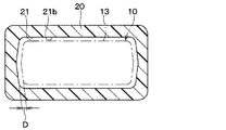
第1実施形態の半導体装置について、図1〜図4を参照して述べる。図2では、後述する挿入穴21に挿入された一次成形体10の外郭線を一点鎖線で示している。
(1st Embodiment)
The semiconductor device according to the first embodiment will be described with reference to FIGS. In FIG. 2, the outline of the primary molded
本実施形態では、圧力センサとされた半導体装置を例に挙げて説明する。なお、本実施形態の圧力センサは、例えば、自動車のエンジンを被取付部材として取り付けられ、当該エンジンにおける燃焼室内の圧力を検出するのに利用されると好適である。 In the present embodiment, a semiconductor device serving as a pressure sensor will be described as an example. The pressure sensor according to the present embodiment is preferably used, for example, when an automobile engine is attached as a member to be attached, and the pressure sensor is used to detect a pressure in a combustion chamber of the engine.
本実施形態の半導体装置は、図1に示すように、半導体チップ12を備える一次成形体10と、一次成形体10の一部が挿入された筐体部品20と、一次成形体10の一部および筐体部品20の一部を一体的に覆う二次成形樹脂30とを有してなる。
As shown in FIG. 1, the semiconductor device according to the present embodiment includes a primary molded
一次成形体10は、図1に示すように、回路基板11と、回路基板11上に搭載された半導体チップ12と、回路基板11の一部を封止する一次成形樹脂13と、回路基板11と電気的に接続された電気接続部材14とを有してなる。そして、回路基板11のうち半導体チップ12が搭載された側を一端11aとして、回路基板11のうち一端11aの反対側の他端11bは、一次成形樹脂13から露出すると共に、電気接続部材14と電気的に接続されている。また、半導体チップ12は、本実施形態では、半導体チップ12が搭載された回路基板11の一面に対する法線方向において一次成形樹脂13から露出している。
As shown in FIG. 1, the primary molded
図1に示すように、本実施形態では、一次成形樹脂13のうち回路基板11の一端11a側を覆う領域を一端側13aとし、その反対側を他端側13bとして、一次成形体10のうち一端側13aが後述する筐体部品20に形成された挿入穴21に挿入されている。一次成形体10のうち他端側13bは、本実施形態では、筐体部品20の挿入穴21から突出し、筐体部品20から露出している。筐体部品20から露出した一次成形体10の他端側13bのうち電気接続部材14の端部14aを除く残部は、後述する二次成形樹脂30により覆われている。そして、電気接続部材14の端部14aは、二次成形樹脂30から突出し、二次成形樹脂30から露出している。
As shown in FIG. 1, in the present embodiment, a region of the
一次成形体10は、例えば、半導体チップ12が搭載され、電気接続部材14と電気的に接続された回路基板11を図示しない金型にセットし、一次成形樹脂13をトランスファー成形やコンプレッション成形等の成形および熱硬化処理を行うことで形成される。
The primary molded
なお、ここでいう「一次成形」とは、後述する二次成形樹脂30を成形する工程を二次成形と捉えた場合、その前工程である一次成形体10を成形する工程を意味する。
In addition, the term “primary molding” as used herein means a step of molding the primary molded
回路基板11は、一面を有し、その一面上に半導体チップ12が搭載されている。回路基板11のうち半導体チップ12が搭載されている一端11a側が一次成形樹脂13により封止されると共に、その反対側である他端11b側が一次成形樹脂13から露出している。
The
なお、回路基板11は、基板に導電材料によりなる回路配線が形成されたものであってもよいし、金属によりなる金属板を加工して得られるアイランド部とリード部とを有するリードフレームであってもよい。
Note that the
半導体チップ12は、例えばSi等の半導体材料によりなり、導電性接着剤等を介して回路基板11上に搭載されている。例えば、半導体チップ12は、周囲の測定媒体の圧力、磁気、光量等物理量に応じた電気出力を発生するように構成された検出部を備えており、ワイヤ等により回路基板11と電気的に接続されると共に、公知の半導体プロセスにより形成される。半導体チップ12は、本実施形態では、圧力を検出する検出部を備え、測定媒体に晒されるように一次成形樹脂13から露出している。そして、半導体チップ12は、図1に示すように、後述する筐体部品20の内部空間24に面するように配置され、筐体部品20の内部空間24へ繋がる開口部24aから導入される測定媒体の圧力に応じた電気信号を出力する。
The
一次成形樹脂13は、例えばエポキシ樹脂等の熱硬化性樹脂によりなり、図1に示すように回路基板11の一部を覆うと共に、半導体チップ12を露出させるための凹部13cが形成されている。一次成形樹脂13は、例えばトランスファー成形やコンプレッション成形等の成形および熱硬化処理を行うことにより形成される。
The
なお、一次成形樹脂13には、線膨張係数の調整等の観点から、必要に応じて、シリカやアルミナ等の絶縁性材料によりなるフィラーが含有されていてもよい。また、後述する二次成形樹脂30との密着性向上の観点から、二次成形樹脂30に添加剤を含有させる場合には、当該添加剤と官能基を有する他の添加剤が添加されていてもよい。
The
電気接続部材14は、図示しない導電性接着剤等を介して、一次成形樹脂13から露出した回路基材11の他端11b側と電気的に接続されている。なお、本実施形態では、電気接続部材14としてターミナル端子を用いた例を示しているが、回路配線が形成された回路基板を電気接続部材14として用いてもよい。
The
筐体部品20は、後述する製造工程において一次成形体10を挿入して嵌め込んで固定しつつ、二次成形樹脂30のインサート成形時に一次成形体10にかかる荷重を吸収することで、一次成形体10の反りやクラック等の発生を抑制する役割を果たす。
The
筐体部品20は、例えば、エポキシ樹脂等の熱硬化性樹脂やPPS(ポリフェニレンサルファイド)等の熱可塑性樹脂等の樹脂材料によりなる弾性体であり、トランスファー成形や射出成形等の成形および熱処理等を行うことにより形成される。筐体部品20は、一次成形体10の挿入時における位置ズレ抑制や上記の一次成形体10にかかる荷重の吸収等の観点から、一次成形体10のうち一次成形樹脂13の材料よりも弾性率や線膨張係数が大きい材料により構成されることが好ましい。筐体部品20による一次成形体10にかかる荷重の吸収等の作用については、後述する製造工程にて詳しく説明する。
The
なお、筐体部品20は、線膨張係数の調整の観点から、Si等の絶縁材料等によるフィラーが添加されてもよい。また、筐体部品20は、二次成形樹脂30との密着向上の観点から、二次成形樹脂30に官能基を有する添加剤を添加する場合には、当該官能基と反応する官能基を有する添加剤が添加されていてもよい。
The
筐体部品20は、図1に示すように、一次成形体10のうち半導体チップ12を含む部分を挿入するための挿入穴21が形成されている。そして、一次成形体10の表面のうち挿入穴21が伸びる方向(以下「挿入方向」という)における面を挿入面10aとして、挿入方向から挿入穴21を見たときの挿入穴21の底面21aは、挿入面10aの一部と接触している。
As shown in FIG. 1, the
具体的には、挿入面10aのうち挿入方向において突き出た先端部10bと異なる部分が底面21aに接触している。すなわち、底面21aは、本実施形態では、挿入穴21に挿入された一次成形体10の挿入面10aの一部を受け止める押さえ面とされている。また、底面21aは、挿入方向に沿って窪んだ窪み部22が形成されている。これは、後述する製造工程において先端部10bと底面21aとが接触したまま、二次成形樹脂30がインサート成形されることにより、荷重が先端部10bにかかることを抑制し、一次成形体10の損傷等を防ぐためである。この詳細については、製造工程の説明にて後述する。
Specifically, a portion of the
図2に示すように、挿入穴21を挿入方向から見たときの挿入穴21の内壁面21bと一次成形体10との隙間Dは、200μm以下とされることが好ましい。隙間Dが200μmを超える場合、一次成形体10を挿入穴21に挿入した時や二次成形樹脂30のインサート成形時における一次成形体10の位置ズレや二次成形樹脂材料30aが当該隙間に過剰に侵入することによる樹脂バリの発生等の不具合が生じ得るためである。
As shown in FIG. 2, when the
筐体部品20は、図1に示すように、挿入方向を軸とする径方向(以下、単に「径方向」という)における寸法が他の筐体部品20の部分の径方向における寸法よりも小さくされた筐体シール部23が形成されている。
As shown in FIG. 1, the
筐体シール部23は、挿入方向から見たとき、略四角形の枠体状とされ、距離を隔てて一次成形体10のうち一次成形樹脂13を囲むように形成されている。筐体シール部23は、図1に示すように、筐体部品20のうち挿入穴21を囲む領域を含む領域であって、一次成形体10のうち挿入穴21から露出した部分と共に二次成形樹脂30により覆われている。筐体シール部23は、本実施形態では、二次成形樹脂30により覆われることで、半導体チップ12にかかる圧力が挿入穴21から外部に漏れないようにシールされた圧力シール部とされている。
The
なお、筐体部品20は、二次成形樹脂30と密着するのであれば、二次成形樹脂30と異なる材料により構成されていてもよいが、二次成形樹脂30と同じ材料により構成されることが好ましい。これは、筐体シール部23の表面が同じ材料同士が一体化して接合される領域となることで、二次成形樹脂30の表面との明確な界面が生じない状態となり、二次成形樹脂30との密着性が向上し、挿入穴21からの圧力漏れを抑制できるためである。
The
また、挿入方向から見て、筐体シール部23の外周部には、図1に示すように、二次成形樹脂30との密着性を高めるための凸部23aが形成されていてもよいし、凸部23aに限らず、アンカー効果を発揮する凹凸が形成された粗化領域等が形成されていてもよい。
In addition, when viewed from the insertion direction, a
筐体部品20は、例えば図示しない燃料パイプ等の被取付対象に直接取り付けられるもので、外周面に被取付対象に取り付けた際のシールをするためのOリング40取付用の溝25が形成されている。このように、例えば燃料パイプに取り付けることによって開口部24aが燃料パイプ内と連通して、内部空間24への測定媒体の導入が可能となる。
The
なお、上記の例では、外部の被取付対象への取付とシールについて説明したが、筐体部品20に外部の被取付対象への取付が可能な構造が形成されていればよく、必要に応じてシール用のOリング40が取り付けられてもよい。例えば、筐体部品20は、外部の被取付対象と螺合して取り付けるためのネジが形成されてもよいし、他の取付構造が形成されてもよい。
In the above example, the attachment and the seal to the external object to be mounted have been described. However, it is sufficient that the
二次成形樹脂30は、例えば、PPSやPBT(ポリブチレンテレフタレート)等の熱可塑性樹脂等の樹脂材料等により構成される。なお、二次成形樹脂30は、一次成形樹脂13や筐体部品20と同様に、絶縁性材料などによるフィラーや添加剤が添加されていてもよい。
The
二次成形樹脂30は、一次成形体10の表面のうち挿入穴21から露出する部分(以下「一次成形体露出部」という)および筐体部品20のうち筐体シール部23を覆う部材である。つまり、二次成形樹脂30は、一次成形体露出部および筐体シール部23と密着しており、これら2つの部位との界面で圧力シール部を形成している。二次成形樹脂30は、例えば一次成形体10を筐体部品20の挿入穴21に挿入したものを金型にセットした後に、溶融した熱可塑性樹脂材料等を流し込んで冷却して硬化するインサート成形により形成される。
The
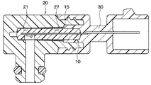
以上が、本実施形態の半導体装置の基本的な構成である。次に、本実施形態の半導体装置の製造工程について、図3、図4を参照して説明する。図4では、後述する二次成形樹脂30のインサート成形時における筐体部品20による一次成形体10の位置ズレ抑制を分かり易くするため、一次成形体10の一部、二次成形樹脂材料30aおよび金型については省略している。
The above is the basic configuration of the semiconductor device of the present embodiment. Next, a manufacturing process of the semiconductor device of the present embodiment will be described with reference to FIGS. In FIG. 4, a part of the primary molded
まず、図3(a)に示す一次成形体10を用意する。一次成形体10は、例えば、回路基板11を図示しない金型を用いて一次成形樹脂13によりモールドした後に、当該回路基板11のうち凹部13cに半導体チップ12を実装し、電気接合部材14と接続することで得られる。
First, a primary molded
その後、挿入穴21が形成された筐体部品20を用意し、図3(b)に示すように、挿入穴21に一次成形体10を挿入する。このとき、図2に示すように、挿入穴21を挿入方向から見たときの内壁面21bと一次成形体10との隙間Dを200μm以下とする。このように、内壁面21bと一次成形体10との隙間Dを200μm以下の低クリアランスとし、挿入穴21に一次成形体10を嵌め込むことにより、一次成形体10の位置ズレを抑制できる。
After that, the
この際、次の二次成形樹脂30のインサート成形における金型内での加熱によって、隙間Dが狭まって筐体部品20が一次成形体10を押さえ付けるようにするために、筐体部品20および一次成形樹脂13の材料の線膨張係数を調整することが好ましい。これは、図4に示すように、次工程の二次成形樹脂30のインサート成形時に金型で筐体部品20および一次成形体10が加熱される際に、筐体部品20の熱膨張により一次成形体10が押さえ付けられ、一次成形体10の位置ズレを抑制することができるためである。
At this time, in order to make the gap D narrow and the
具体的には、例えば、加熱に伴う熱膨張によって隙間Dが狭くなるように、筐体部品20を線膨張係数が大きな材料で構成しつつ、一次成形体10のうち一次成形樹脂13を筐体部品20の材料よりも線膨張係数の小さい材料で構成する。これにより、筐体部品20および一次成形体10が金型内で加熱された際に、筐体部品20の寸法変化により図4に示す矢印の向きの力、すなわち一次成形体10を押さえ付ける力が生じ、この力を利用して一次成形体10の位置ズレを抑制できる。
Specifically, for example, while the
また、図3(b)に示すように、一次成形体10を挿入穴21に挿入したとき、挿入方向から見て、一次成形体10のうち挿入面10aの先端部10bが筐体部品20に形成された窪み部22上になるようにすることが好ましい。言い換えると、一次成形体10の先端部10bが筐体部品20の底面21aに接触しないようにすると共に、一次成形体10の挿入面10aのうち先端部10bと異なる部分を底面21aに接触させることが好ましい。これは、後述する二次成形樹脂30のインサート成形時に一次成形体10にかかる荷重が先端部10bに集中することを回避し、回路基板11およびこれに搭載された半導体チップ12等に残留応力が生じることによる半導体装置の信頼性の低下を回避するためである。
As shown in FIG. 3B, when the primary molded
具体的には、一次成形体10は、挿入方向のうち先端部10bを通る直線上に回路基板11が配置されているため、先端部10bと筐体部品20の底面21aとが接触することにより先端部10bに過剰に荷重がかかると、回路基板11にもその力が伝わってしまう。すると、回路基板11に挿入方向の反対方向に力がかかり、回路基板11に残留応力が生じ、回路基板11上に搭載された半導体チップ12等にもその影響が生じ得る。その結果、一次成形体10の損傷等の不具合が生じることが懸念される。
Specifically, in the primary molded
そこで、先端部10bが筐体部品20の底面21aに接触しないように、筐体部品20の底面21aに窪み部22を設け、一次成形体10の挿入面10aのうち先端部10bと異なる部分を底面21aに接触させることで、上記の不具合が生じるのを回避できる。
Therefore, a
その後、図3(c)に示すように、例えば、筐体部品20に一次成形体10が挿入されたものを上型100、下型101およびスライド型102によりなる金型にセットし、熱可塑性樹脂によりなる二次成形樹脂材料30aを当該金型内に注入する。これにより、二次成形樹脂材料30aが、一次成形体10のうち一次成形体露出部から電気接合部材14の端部14aを除く部分および筐体部品20の表面のうち挿入穴21を囲む領域を含む一部を覆った状態となる。その後、二次成形樹脂材料30aを硬化させることで、一次成形体10の一部および筐体部品20の一部を覆う二次成形樹脂30が得られ、図1に示す本実施形態の半導体装置を製造できる。
After that, as shown in FIG. 3C, for example, the one in which the primary molded
本実施形態の半導体装置によれば、一次成形体10が筐体部品20の挿入穴21に挿入されつつ、一次成形体10のうち一次成形体露出部と筐体部品20のうち筐体シール部23とを二次成形樹脂30が覆う構造となる。そのため、筐体部品20が二次成形樹脂30と広い面積で接合されるため、従来の半導体装置に比べて接合の信頼性の高い半導体装置となる。また、一次成形体10が筐体部品20の挿入穴21に挿入された構造であるため、従来の半導体装置に比べて、一次成形体10の反りが抑制された半導体装置となる。
According to the semiconductor device of the present embodiment, the primary molded
本実施形態の半導体装置の製造方法によれば、一次成形体10を筐体部品20の挿入穴21に挿入した後に二次成形樹脂30をインサート成形するため、二次成形樹脂30を金型内に注入する際、一次成形体10にかかる荷重は挿入方向に沿ったものとなる。そして、樹脂材料等の弾性体で構成された筐体部品20が、挿入穴21の底面21aで一次成形体10を受け止めることにより、一次成形体10にかかる荷重を吸収する。そのため、当該半導体装置の製造工程において、一次成形体10にかかる二次成形樹脂材料30aによる荷重を緩和でき、一次成形体10でのクラック発生が抑制される。
According to the method for manufacturing a semiconductor device of the present embodiment, the
また、筐体部品20に一次成形体10を挿入して、筐体部品20のうち筐体シール部23と二次成形樹脂30とが接合されるため、従来の半導体装置に比べて接合面積が大きくなり、接合信頼性が高い半導体装置を製造できる。
Further, since the primary molded
さらに、筐体部品20の挿入穴21に一次成形体10を挿入して二次成形樹脂30のインサート成形をするため、一次成形体10が一面だけでなく外周面全体で固定されると共に、一次成形体10にかかる荷重が挿入方向に限定される。そのため、従来の半導体装置に比べて、当該インサート成形の荷重による一次成形体10の反りが抑制された半導体装置を製造できる。
Furthermore, since the primary molded
(第2実施形態)
第2実施形態の半導体装置について、図5〜図7を参照して述べる。図6では、二次成形樹脂30のインサート成形における一次成形体10への荷重の吸収について分かり易くするために、図5中に示す領域R以外の要素については省略している。また、図7では、挿入穴21に挿入された一次成形体10の外郭線を一点鎖線で示している。
(2nd Embodiment)
The semiconductor device according to the second embodiment will be described with reference to FIGS. In FIG. 6, elements other than the region R shown in FIG. 5 are omitted in order to make it easier to understand the absorption of the load to the primary molded
本実施形態の半導体装置は、図5もしくは図6に示すように、筐体部品20の挿入穴21の底面21aに窪み部22が形成されておらず、二次成形樹脂30のインサート成形時に一次成形体10にかかる荷重を吸収するための受け止め部21cが形成されている。また、本実施形態の半導体装置は、図7に示すように挿入穴21の内壁面21bに、一次成形体10に向かって突き出し、一次成形体10の位置ズレを抑制するためのリブ26が形成されている。本実施形態の半導体装置は、これらの点が上記第1実施形態と相違する。本実施形態では、これらの相違点について主に説明する。
As shown in FIG. 5 or FIG. 6, the semiconductor device of the present embodiment does not have the
筐体部品20は、図5もしくは図6に示すように、挿入穴21の底面21aから挿入方向の反対方向に向かって突き出し、二次成形樹脂30のインサート成形において一次成形体10にかかる荷重を吸収するための受け止め部21cが形成されている。
As shown in FIG. 5 or FIG. 6, the
受け止め部21cは、図6(a)に示すように、一次成形体10が挿入穴21に挿入される前においては、挿入方向の反対方向に向かって突き出した形状とされている。そして、受け止め部21cは、図6(a)に示すように、一次成形体10が挿入された後の二次成形樹脂30のインサート成形時においては、一次成形体10にかかる荷重を受けて変形し、当該荷重を吸収する働きをする。この際、受け止め部21cは、上記第1実施形態における底面21aと同様に、一次成形体10のうち挿入面10aのうち先端部10bと異なる部分と接触し、先端部10bに荷重がかからない配置とされている。
As shown in FIG. 6A, the receiving
なお、受け止め部21cの形状、高さおよび数等については、任意であり、一次成形体10の先端部10bに荷重がかからないのであれば、他の形状等とされていてもよい。このように、筐体部品20は、受け止め部21cが底面21aに形成される場合等には、窪み部22が底面21aに形成されていなくてもよい。
The shape, height, number, and the like of the receiving
筐体部品20の内壁面21bには、図7に示すように、径方向に対して突き出すと共に、挿入穴21に挿入される一次成形体10の位置ズレを抑制するためのリブ26が形成されている。リブ26が形成されている部分以外においては、内壁面21bと一次成形体10との隙間Dは、上記第1実施形態と同様に200μm以下とされていることが好ましい。言い換えると、このような隙間Dとされた場合、リブ26は、内壁面21bのうち当該リブが形成された一面に対する法線方向における高さが200μm以下とされる。
As shown in FIG. 7,
なお、本実施形態においても筐体部品20を樹脂材料等によりなる弾性体により構成することで、リブ26が形成された筐体部品20を図示しない金型を用いて成形しても、当該金型から容易に引き抜くことができる。また、リブ26の形状や形成する数や配置等については、任意であり、図7に示ように断面形状が台形状とされた例に限らず、断面形状が半円形状や他の形状とされてもよく、形成する数や配置等については適宜変更されてもよい。
Also in the present embodiment, by forming the
本実施形態によれば、上記第1実施形態と同様、一次成形体10が挿入穴21に挿入された状態で筐体部品20が二次成形樹脂30と広面積で接合された構造のため、従来の半導体装置に比べ、一次成形体10の反りが少なく、接合信頼性の高い半導体装置となる。また、受け止め部21cにより一次成形体10にかかる荷重が吸収されると共に、リブ26により一次成形体10の位置ズレが抑制される構造であるため、従来の半導体装置に比べて、一次成形体10のクラック等の不具合がより抑制された半導体装置となる。
According to the present embodiment, similarly to the first embodiment, since the
また、受け止め部21cおよびリブ26を備える筐体部品20を用いることで、一次成形体10の位置ズレを抑制しつつ、従来の半導体装置に比べて、一次成形体10のクラック等の不具合がより抑制された半導体装置を安定して製造することができる。
In addition, by using the
(第3実施形態)
第3実施形態の半導体装置について、図8を参照して述べる。本実施形態の半導体装置は、図8に示すように、筐体部品20の内壁面21bに挿入方向の反対方向に向かうにつれて径方向の寸法が大きくなる勾配面27が設けられている。そして、一次成形体10のうち一次成形樹脂13に当該勾配に沿って径方向の寸法が大きくなるように勾配追従突起15が形成されている。本実施形態の半導体装置は、これらの点が上記第1実施形態と相違する。本実施形態では、これらの相違点について主に説明する。
(Third embodiment)
A semiconductor device according to a third embodiment will be described with reference to FIG. In the semiconductor device of the present embodiment, as shown in FIG. 8, a
筐体部品20は、例えば、図示しない金型を用いて射出成形等により形成されるが、形成後に当該金型から筐体部品20を取り出しやすくするために、挿入穴21に挿入方向の反対方向に向かうにつれて径方向の寸法が大きくなる勾配面27が設けられている。
The
このように金型からの取り出しを行いやすい勾配面27が設けられた筐体部品20を用いる場合には、図8に示すように、一次成形体10に勾配面27に沿って径方向の寸法が大きくされた勾配追従突起15が形成されていることが好ましい。挿入方向から見たときの内壁面21bと一次成形体10との隙間が大きくなり過ぎないようにし、一次成形体10の挿入時や二次成形樹脂30のインサート成形時における一次成形体10の位置ズレを抑制できるためである。
When using the
なお、勾配追従突起15は、勾配面27に沿った形状とされていればよく、一次成形樹脂13の外周の一部に形成されていてもよいし、全域に形成されていてもよい。また、勾配面27については、挿入方向の反対方向へ向かう際の傾きが一定とされてもよく、当該傾きが徐々に大きくされてもよいし、段階的に傾きが大きくされてもよい。勾配面27の傾きについては、任意である。
Note that the
本実施形態によれば、挿入穴21に勾配面27が形成された筐体部品20を用いたとしても、上記第1実施形態と同様に、従来の半導体装置に比べ、一次成形体10の反りやクラック等の不具合が少なく、接合の信頼性の高い半導体装置となる。
According to the present embodiment, even when the
また、金型から抜きやすい形状とされた挿入穴21を備えた筐体部品20を用いることにより、一次成形体10の反りやクラック等の不具合が少なく、接合の信頼性の高い半導体装置を安定して製造することができる。
In addition, by using the
(第4実施形態)
第4実施形態の半導体装置について、図9を参照して述べる。本実施形態の半導体装置は、図9に示すように、一次成形体10にバリ抑制突起16が形成され、当該バリ抑制突起16に対応して、挿入穴21の径方向の寸法が大きくされた大径部28が筐体部品20に形成されている点が上記第1実施形態と相違する。本実施形態では、この相違点について主に説明する。
(Fourth embodiment)
A semiconductor device according to a fourth embodiment will be described with reference to FIG. In the semiconductor device of the present embodiment, as shown in FIG. 9, the
バリ抑制突起16は、一次成形体10のうち一次成形樹脂13の外周部分に形成され、当該外周から径方向へと突き出す形状、例えば、図9に示すように断面形状が台形形状とされた環状の突起とされる。バリ抑制突起16は、二次成形樹脂30のインサート成形時において挿入穴21の内壁面21bと一次成形体10との間に二次成形樹脂材料30aが入り込み、樹脂バリが生じることを抑制するために一次成形体10に形成される。
The
具体的には、二次成形樹脂30のインサート成形時にバリ抑制突起16により、挿入穴21側への二次成形樹脂材料30aの流れがせき止められる。また、二次成形樹脂材料30aのうちバリ抑制突起16を乗り越えたものについては、大径部28と一次成形体10との隙間のうちバリ抑制突起16を超えた先の空間に留まる。そのため、挿入穴21のうち大径部28よりも径方向の寸法が小さくされた内壁面21bと一次成形体10との間に二次成形樹脂材料30aが過剰に入り込むことが抑制され、これらの間に樹脂バリが生じることを抑制できる。
Specifically, at the time of insert molding of the
筐体部品20は、本実施形態では、図9に示すように、一次成形体10が挿入される挿入穴21のうち挿入方向の反対方向側に、挿入穴21の径方向における寸法(以下「挿入穴寸法」という)よりも径方向の寸法が大きくされた大径部28が形成されている。大径部28の径方向における寸法(以下「大径部寸法」という)は、バリ抑制突起16の高さ寸法、すなわち一次成形樹脂13の外周のうちバリ抑制突起16が形成された一面に対する法線方向における寸法に合わせて調整される。具体的には、大径部寸法は、挿入穴寸法にバリ抑制突起16の高さ寸法を足して得られる寸法以上とされていればよい。
In the present embodiment, as shown in FIG. 9, the
なお、バリ抑制突起16は、二次成形樹脂材料30aの一部もしくは全部を受け止めることができる形状とされていればよく、図9に示すように断面形状が台形形状とされた例に限られず、断面形状が半円形状とされたり、他の任意の形状とされたりしてもよい。バリ抑制突起16は、一次成形体10の外周の一部に断続的に形成されてもよいし、当該外周の全部に連続的に形成されてもよい。また、バリ抑制突起16の高さ寸法および大径部寸法については、任意の数値とされる。
Note that the
本実施形態によれば、バリ抑制突起16により樹脂バリの発生およびこれによる不具合が抑制されると共に、上記第1実施形態と同様に、従来の半導体装置に比べ、一次成形体10の反りやクラック等の不具合が少なく、接合の信頼性の高い半導体装置となる。
According to the present embodiment, the occurrence of resin burrs and the problems caused by the burrs are suppressed by the
(第5実施形態)
第5実施形態の半導体装置について、図10を参照して述べる。本実施形態の半導体装置は、図10に示すように、半導体チップ12のうち図示しない検出部を含む一部の領域が挿入方向に沿って挿入面10aから露出している。また、本実施形態の半導体装置は、挿入穴21の内壁面21bから挿入方向に沿って交差する方向に突き出した突起29が形成され、突起29と挿入面10aとが接触した構造とされている。本実施形態の半導体装置は、これらの点が上記第1実施形態と相違する。本実施形態では、これらの相違点について主に説明する。
(Fifth embodiment)
A semiconductor device according to a fifth embodiment will be described with reference to FIG. In the semiconductor device of the present embodiment, as shown in FIG. 10, a part of the
筐体部品20は、本実施形態では、図10に示すように、半導体チップ12のうち検出部を含む一部の領域が挿入面10aから露出した構造とされた一次成形体10と挿入穴21の底面21aとが接触しないように突起29が形成されている。具体的には、筐体部品20は、挿入穴21の内壁面21bに挿入方向と交差する方向に突き出す突起29が形成されている。
In the present embodiment, as shown in FIG. 10, the
突起29は、一次成形体10の挿入面10aのうち先端部10bと異なる部分に接触する押さえ面29aが形成されている。突起29は、内壁面21bのうち当該突起29が形成された一面に対する法線方向における寸法が半導体チップ12と接触しない程度とされている。つまり、突起29は、半導体チップ12が筐体部品20に接触して破損することを防止しつつ、一次成形体10の挿入穴21への挿入時および二次成形樹脂30のインサート成形時に一次成形体10を受け止め、一次成形体10にかかる荷重を吸収する役割を果たす。
The
なお、突起29は、半導体チップ12に接触せず、かつ挿入面10aに接触して一次成形体10を受け止めることができればよく、図10に示す例に限らず、例えば半導体チップ12を四方から取り囲むように形成されてもよいし、他の配置で形成されてもよい。
In addition, the
本実施形態によれば、半導体チップ12の一部が挿入面10aから露出した構造とされていても、上記第1実施形態と同様に、従来の半導体装置に比べ、一次成形体10の反りやクラック等の不具合が少なく、接合の信頼性の高い半導体装置となる。
According to the present embodiment, even when the
また、半導体チップ12が挿入面10aから露出した一次成形体10を用いたとしても、半導体チップ12の破損を防止しつつ、一次成形体10の反りやクラック等の不具合が少なく、接合の信頼性の高い半導体装置を製造することができる。
Further, even if the primary molded
(第6実施形態)
第6実施形態の半導体装置について、図11〜図13を参照して述べる。本実施形態の半導体装置は、図11に示すように、一次成形体10と二次成形樹脂30とが一体化されたものが金属材料によりなる筐体部品20に接続された構造とされている点で上記第5実施形態と異なる。本実施形態では、この相違点について主に説明する。
(Sixth embodiment)
A semiconductor device according to a sixth embodiment will be described with reference to FIGS. As shown in FIG. 11, the semiconductor device of the present embodiment has a structure in which an integrated primary molded
筐体部品20は、本実施形態では、例えば一次成形体10の一部が挿入される中空部20cと収容領域20dとが設けられ、収容領域20dが形成された部分の径が、中空部20cが形成された部分の径よりも大きくされたフランジ形状とされている。筐体部品20は、図11に示すように、上記各実施形態と異なり、二次成形樹脂30の一部を覆うように、一次成形体10と二次成形樹脂30とが一体化されたもの(以下、本実施形態において「二次成形体」という)とかしめて接続されている。
In the present embodiment, the
具体的には、筐体部品20は、図11に示すように、例えば収容領域20dの底面に相当する一面20aにおいて、二次成形体とOリング40を介してシールされている。また、一次成形体10のうち半導体チップ12の検出部を含み、二次成形樹脂30から露出する部分は、中空部20cに収容されている。そして、半導体チップ12の検出部は、筐体部品20に形成され、中空部20cに繋がる開口部20bから導入される測定媒体の圧力に応じた電気出力を出力する。
Specifically, as shown in FIG. 11, the
なお、筐体部品20は、上記各実施形態と同様の樹脂材料により構成されてもよいし、金属材料により構成されてもよい。
The
次に、本実施形態の半導体装置の製造方法について、図12、図13を参照して説明する。 Next, a method of manufacturing the semiconductor device according to the present embodiment will be described with reference to FIGS.
半導体チップ12のうち検出部を含む一部が一次成形樹脂13から露出した一次成形体10については、例えば上記各実施形態と同様に、図示しない金型等を用いてトランスファー成形等により成形される。
The primary molded
その後、図12(a)に示すように、例えばPPSなどの熱可塑性樹脂材料などの弾性体によりなる保護キャップ50を、一次成形体10のうち半導体チップ12の露出部を覆うように取り付ける。
Thereafter, as shown in FIG. 12A, a
そして、図12(b)に示すように、保護キャップ50を取り付けた一次成形体10を、上型100、下型101およびスライド型102によりなる金型にセットする。そして、当該金型内に二次成形樹脂30aを注入して硬化することで、図12(c)に示す保護キャップが取り付けられた二次成形体が得られる。
Then, as shown in FIG. 12B, the primary molded
続けて、図12(c)に示す二次成形体から保護キャップ50を取り外し、Oリング40を取り付けた後、筐体部品20とかしめてシールすることにより、図11に示す本実施形態の半導体装置を製造することができる。
Subsequently, the
なお、図13に示すように、図12(b)に示したスライド型102と別のスライド型103に保護キャップ50を挿入したものを用いてもよく、金型については、適宜任意のものを用いてもよい。保護キャップ50を挿入したスライド型103を用いる場合、二次成形樹脂30を形成後に、上型100、下型101およびスライド型102を取り外してから二次成形体をスライド型103から引き抜くと、保護キャップ50を繰り返し使用することも可能となる。
As shown in FIG. 13, the one in which the
本実施形態によれば、筐体部品20が一次成形体10を受け止めつつ、二次成形樹脂30のインサート成形をすることができない構造であっても、従来の半導体装置に比べて、一次成形体10の反りやクラック等が抑制された半導体装置となる。
According to the present embodiment, even if the
また、二次成形樹脂30をインサート成形する際において一次成形体10にかかる荷重を筐体部品20で吸収することができない構造の一次成形体10を用いる場合であっても、保護キャップ50を用いることで半導体チップ12の破損を防止できる。そして、保護キャップ50を取り外した二次成形体を筐体部品20と接続することで、従来の半導体装置に比べて、一次成形体10の反りやクラック等が抑制された半導体装置を製造することができる。
Further, even when the primary molded
(他の実施形態)
なお、上記した各実施形態に示した半導体装置は、本発明の半導体装置およびその製造方法の一例を示したものであり、上記の各実施形態に限定されるものではなく、特許請求の範囲に記載した範囲内において適宜変更が可能である。
(Other embodiments)
The semiconductor device described in each of the above embodiments is an example of the semiconductor device of the present invention and a method for manufacturing the same, and is not limited to each of the above embodiments. Changes can be made as appropriate within the described range.
例えば、上記各実施形態の半導体装置では、一次成形樹脂13が熱硬化性樹脂により構成された例について説明したが、PPS等の熱可塑性樹脂により構成されてもよい。この際、半導体チップ12と回路基板11とがワイヤ接続されている場合には、ワイヤが熱可塑性樹脂により断線しないように留意する。
For example, in the semiconductor device of each of the above-described embodiments, an example has been described in which the
上記各実施形態では、半導体チップ12として圧力を検出する素子を用い、半導体装置が全体として圧力センサとされた例について説明したが、これに限られず、半導体チップ12として、磁気や光量などの他の物理量を検出する素子を用いてもよい。この場合、半導体チップ12については、一次成形樹脂13により封止されていてもよく、筐体部品20のうち中空空間24を備える部分については、任意の磁気センサや光量センサ等の形状等に合わせてその形状等が適宜変更されてもよい。
In each of the above embodiments, an example was described in which an element for detecting pressure was used as the
上記の第1実施形態ないし第5実施形態の各実施形態については、それぞれを組み合わせた構造の半導体装置とされてもよい。例えば、第1実施形態の半導体装置や第5実施形態の半導体装置に、第2実施形態の半導体装置において形成されていたリブ26や受け止め部21cが形成されてもよく、他の各実施形態同士を適宜組み合わせた構造の半導体装置とされてもよい。
Each of the first to fifth embodiments described above may be a semiconductor device having a combined structure. For example, the semiconductor device according to the first embodiment or the semiconductor device according to the fifth embodiment may be formed with the
上記第1実施形態ないし第5実施形態では、挿入穴21の底面もしくは内壁面のうち一次成形体10の挿入面10aに接触する面が押さえ面とされた例について説明した。しかし、図14に示すように、一次成形体10のうち一次成形樹脂13が径方向に突出する部分を備える形状とされている場合、一次成形樹脂13のうち当該突出部分の段差における側面13dを受ける押さえ面21dが挿入穴21に形成された構造とされてもよい。この場合、図14に示すように、挿入面10aが挿入穴21の底面21aに接触していなくても、押さえ面21dが側面13dに接触することで一次成形体10を受け止め、一次成形体10にかかる荷重を吸収できる。なお、挿入面10aが底面21aに接触すると共に、押さえ面21dが側面13dに接触する構造の半導体装置とされてもよい。
In the above-described first to fifth embodiments, an example has been described in which the surface of the bottom surface or the inner wall surface of the
上記第1実施形態ないし第5実施形態では、筐体部品20が樹脂材料により構成された弾性体である例について説明した。しかし、筐体部品20は、二次成形樹脂30のインサート成形時に一次成形体10にかかる荷重を吸収できるものであればよく、Al等の比較的軟らかい金属材料により構成されてもよい。例えば、筐体部品20をAlにより構成すると共に、微細な凸部とされた受け止め部21cが形成されたものとすることで、二次成形樹脂30のインサート成形時に一次成形体10にかかる荷重を吸収でき、一次成形体10のクラック等が抑制された半導体装置となる。
In the first to fifth embodiments, examples in which the
10 一次成形体
10a 挿入面
12 半導体チップ
13 一次成形樹脂
20 筐体部品
21 挿入穴
21a 底面
21c 受け止め部
22 窪み部
30 二次成形樹脂
DESCRIPTION OF
Claims (16)
前記一次成形体が挿入されるための挿入穴(21)が形成された筐体部品(20)と、
樹脂材料によりなり、前記一次成形体の表面のうち前記挿入穴から露出した領域と前記筐体部品の表面のうち前記挿入穴を囲む領域を含む一部の領域とを一体的に覆う二次成形樹脂(30)と、を備え、
前記一次成形体のうち前記半導体チップを含む部分は、前記挿入穴に挿入されており、
前記一次成形体は、前記挿入穴が伸びる方向を挿入方向として、前記挿入方向を軸とする径方向に沿って突き出たバリ抑制突起(16)が形成されると共に、前記バリ抑制突起が前記挿入穴に挿入されている半導体装置。 A primary molded body (10) including a semiconductor chip (12) having a detection unit for detecting a physical quantity and a primary molded resin (13) made of a resin material;
A housing component (20) having an insertion hole (21) for inserting the primary molded body,
Secondary molding made of a resin material and integrally covering a region of the surface of the primary molded body exposed from the insertion hole and a part of a surface of the housing component including a region surrounding the insertion hole. A resin (30);
A portion including the semiconductor chip in the primary molded body is inserted into the insertion hole ,
The primary molded body is formed with a burr suppressing projection (16) protruding in a radial direction about the insertion direction, with the direction in which the insertion hole extends as an insertion direction, and the burr suppressing protrusion is inserted into the primary molded body. A semiconductor device inserted in a hole .
前記一次成形体が挿入されるための挿入穴(21)が形成された筐体部品(20)と、A housing component (20) having an insertion hole (21) for inserting the primary molded body,
樹脂材料によりなり、前記一次成形体の表面のうち前記挿入穴から露出した領域と前記筐体部品の表面のうち前記挿入穴を囲む領域を含む一部の領域とを一体的に覆う二次成形樹脂(30)と、を備え、Secondary molding made of a resin material and integrally covering a region of the surface of the primary molded body exposed from the insertion hole and a part of a surface of the housing component including a region surrounding the insertion hole. A resin (30);
前記一次成形体のうち前記半導体チップを含む部分は、前記挿入穴に挿入されており、A portion including the semiconductor chip in the primary molded body is inserted into the insertion hole,
前記挿入穴の内部には、前記挿入穴が伸びる方向を挿入方向とし、前記一次成形体の表面のうち前記挿入方向における面を挿入面(10a)として、前記挿入面のうち前記挿入方向に沿って突き出た先端部(10b)と異なる部分に接触し、前記一次成形体を受け止めるための押さえ面(21a、29a)が形成されており、Inside the insertion hole, a direction in which the insertion hole extends is defined as an insertion direction, and a surface in the insertion direction of the surface of the primary molded body is defined as an insertion surface (10a). A pressing surface (21a, 29a) for contacting a portion different from the protruding tip portion (10b) and receiving the primary molded body;
前記押さえ面(29a)は、前記挿入穴を前記挿入方向から見たときの前記挿入穴の内壁面に形成され、前記内壁面から前記挿入方向と交差する方向に突き出した突起(29)のうち前記挿入面側の面である半導体装置。The pressing surface (29a) is formed on an inner wall surface of the insertion hole when the insertion hole is viewed from the insertion direction, and is formed of a protrusion (29) protruding from the inner wall surface in a direction intersecting the insertion direction. A semiconductor device which is the surface on the insertion surface side.
前記一次成形体が挿入されるための挿入穴(21)が形成された筐体部品(20)と、A housing component (20) having an insertion hole (21) for inserting the primary molded body,
樹脂材料によりなり、前記一次成形体の表面のうち前記挿入穴から露出した領域と前記筐体部品の表面のうち前記挿入穴を囲む領域を含む一部の領域とを一体的に覆う二次成形樹脂(30)と、を備え、Secondary molding made of a resin material and integrally covering a region of the surface of the primary molded body exposed from the insertion hole and a part of a surface of the housing component including a region surrounding the insertion hole. A resin (30);
前記一次成形体のうち前記半導体チップを含む部分は、前記挿入穴に挿入されており、A portion including the semiconductor chip in the primary molded body is inserted into the insertion hole,
前記挿入穴の内部には、前記挿入穴が伸びる方向を挿入方向とし、前記一次成形体の表面のうち前記挿入方向における面を挿入面(10a)として、前記挿入面のうち前記挿入方向に沿って突き出た先端部(10b)と異なる部分に接触し、前記一次成形体を受け止めるための押さえ面(21a、29a)が形成されており、Inside the insertion hole, a direction in which the insertion hole extends is defined as an insertion direction, and a surface in the insertion direction of the surface of the primary molded body is defined as an insertion surface (10a). A pressing surface (21a, 29a) for contacting a portion different from the protruding tip portion (10b) and receiving the primary molded body;
前記押さえ面(21a)は、前記挿入穴を前記挿入方向から見たときの前記挿入穴の底面であり、The pressing surface (21a) is a bottom surface of the insertion hole when the insertion hole is viewed from the insertion direction,
前記筐体部品は、前記挿入方向から見て、前記底面のうち前記先端部と重なる領域に前記底面から前記挿入方向に向かって窪んだ窪み部(22)が形成されている半導体装置。The semiconductor device, wherein the housing component has a recess (22) that is recessed from the bottom surface toward the insertion direction in a region of the bottom surface that overlaps the front end portion when viewed from the insertion direction.
前記一次成形体が挿入されるための挿入穴(21)が形成された筐体部品(20)と、A housing component (20) having an insertion hole (21) for inserting the primary molded body,
樹脂材料によりなり、前記一次成形体の表面のうち前記挿入穴から露出した領域と前記筐体部品の表面のうち前記挿入穴を囲む領域を含む一部の領域とを一体的に覆う二次成形樹脂(30)と、を備え、Secondary molding made of a resin material and integrally covering a region of the surface of the primary molded body exposed from the insertion hole and a part of a surface of the housing component including a region surrounding the insertion hole. A resin (30);
前記一次成形体のうち前記半導体チップを含む部分は、前記挿入穴に挿入されており、A portion including the semiconductor chip in the primary molded body is inserted into the insertion hole,
前記挿入穴の内部には、前記挿入穴が伸びる方向を挿入方向とし、前記一次成形体の表面のうち前記挿入方向における面を挿入面(10a)として、前記挿入面のうち前記挿入方向に沿って突き出た先端部(10b)と異なる部分に接触し、前記一次成形体を受け止めるための押さえ面(21a、29a)が形成されており、Inside the insertion hole, a direction in which the insertion hole extends is defined as an insertion direction, and a surface in the insertion direction of the surface of the primary molded body is defined as an insertion surface (10a). A pressing surface (21a, 29a) for contacting a portion different from the protruding tip portion (10b) and receiving the primary molded body;
前記押さえ面には、前記一次成形体に向かって突出して形成されると共に、前記挿入面のうち前記先端部と異なる部分に接触し、前記一次成形体を受け止める受け止め部(21c)が形成されている半導体装置。A receiving portion (21c) is formed on the pressing surface so as to protrude toward the primary molded body, contacts a portion of the insertion surface different from the tip end portion, and receives the primary molded body. Semiconductor device.
前記一次成形体は、前記勾配に沿って前記径方向における寸法が大きくなる勾配追従突起(15)が形成されている請求項1ないし9のいずれか1つに記載の半導体装置。 With the direction in which the insertion hole extends as the insertion direction, the inner wall surface of the insertion hole when the insertion hole is viewed from the insertion direction has a dimension in a radial direction with the insertion direction as an axis toward the protruding direction. A slope surface (27) that increases is formed,
The semiconductor device according to any one of claims 1 to 9 , wherein the primary molded body is formed with a gradient following protrusion (15) whose dimension in the radial direction increases along the gradient.
前記一次成形体が挿入されるための挿入穴(21)が形成された筐体部品(20)と、
樹脂材料によりなり、前記一次成形体の表面のうち前記挿入穴から露出した領域と前記筐体部品の表面のうち前記挿入穴を囲む領域を含む一部の領域とを一体的に覆う二次成形樹脂(30)と、を備え、
前記一次成形体のうち前記半導体チップを含む部分は、前記挿入穴に挿入されており、
前記挿入穴が伸びる方向を挿入方向として、前記挿入穴を前記挿入方向から見たときの前記挿入穴の内壁面には、前記挿入方向を軸とする径方向における寸法が前記突出方向に向かうにつれて大きくなる勾配面(27)が形成されており、
前記一次成形体は、前記勾配に沿って前記径方向における寸法が大きくなる勾配追従突起(15)が形成されている半導体装置。 A primary molded body (10) including a semiconductor chip (12) having a detection unit for detecting a physical quantity and a primary molded resin (13) made of a resin material;
A housing component (20) having an insertion hole (21) for inserting the primary molded body,
Secondary molding made of a resin material and integrally covering a region of the surface of the primary molded body exposed from the insertion hole and a part of a surface of the housing component including a region surrounding the insertion hole. A resin (30);
A portion including the semiconductor chip in the primary molded body is inserted into the insertion hole,
With the direction in which the insertion hole extends as the insertion direction, the inner wall surface of the insertion hole when the insertion hole is viewed from the insertion direction has a dimension in a radial direction with the insertion direction as an axis toward the projecting direction. A slope surface (27) that becomes larger is formed,
The semiconductor device in which the primary molded body is formed with a gradient follower protrusion (15) whose dimension in the radial direction increases along the gradient .
前記一次成形体のうち前記一次成形樹脂から露出した前記半導体チップに弾性体によりなる保護キャップ(50)を取り付けることと、
前記保護キャップが取り付けられた前記一次成形体を金型にセットして、樹脂材料をインサート成形により前記金型に流し込み、冷却して硬化させることで、前記一次成形体のうち前記保護キャップが取り付けられた部分の反対側を覆う二次成形樹脂(30)を形成することと、
前記一次成形体のうち前記二次成形体から露出する部分を挿入するための挿入穴(21)が形成された筐体部品(20)を用意することと、
前記二次成形樹脂により一部を封止された前記一次成形体から前記保護キャップを取り外した後、これを前記筐体部品に嵌め込むことと、を含む半導体装置の製造方法。 A primary molded body comprising: a semiconductor chip (12) having a detection unit for detecting a physical quantity; and a primary molding resin (13) made of a resin material and sealing a region of the semiconductor chip different from the detection unit. Preparing (10),
Attaching a protective cap (50) made of an elastic body to the semiconductor chip exposed from the primary molding resin in the primary molded body;
The primary molded body to which the protective cap is attached is set in a mold, and a resin material is poured into the mold by insert molding, cooled, and cured, whereby the protective cap is attached to the primary molded body. Forming a secondary molding resin (30) covering the opposite side of the portion provided;
Providing a housing component (20) having an insertion hole (21) for inserting a portion of the primary molded body exposed from the secondary molded body;
A method of manufacturing a semiconductor device, comprising: removing the protective cap from the primary molded body partially sealed with the secondary molding resin, and fitting the protective cap into the housing component.
Priority Applications (4)
| Application Number | Priority Date | Filing Date | Title |
|---|---|---|---|
| JP2017037277A JP6642484B2 (en) | 2017-02-28 | 2017-02-28 | Semiconductor device and method of manufacturing the same |
| CN201880013830.4A CN110366776A (en) | 2017-02-28 | 2018-02-16 | Semiconductor device and its manufacturing method |
| PCT/JP2018/005509 WO2018159329A1 (en) | 2017-02-28 | 2018-02-16 | Semiconductor device and method for manufacturing same |
| US16/526,227 US20190358859A1 (en) | 2017-02-28 | 2019-07-30 | Semiconductor device and method for manufacturing same |
Applications Claiming Priority (1)
| Application Number | Priority Date | Filing Date | Title |
|---|---|---|---|
| JP2017037277A JP6642484B2 (en) | 2017-02-28 | 2017-02-28 | Semiconductor device and method of manufacturing the same |
Publications (3)
| Publication Number | Publication Date |
|---|---|
| JP2018142666A JP2018142666A (en) | 2018-09-13 |
| JP2018142666A5 JP2018142666A5 (en) | 2019-01-17 |
| JP6642484B2 true JP6642484B2 (en) | 2020-02-05 |
Family
ID=63370608
Family Applications (1)
| Application Number | Title | Priority Date | Filing Date |
|---|---|---|---|
| JP2017037277A Expired - Fee Related JP6642484B2 (en) | 2017-02-28 | 2017-02-28 | Semiconductor device and method of manufacturing the same |
Country Status (4)
| Country | Link |
|---|---|
| US (1) | US20190358859A1 (en) |
| JP (1) | JP6642484B2 (en) |
| CN (1) | CN110366776A (en) |
| WO (1) | WO2018159329A1 (en) |
Families Citing this family (4)
| Publication number | Priority date | Publication date | Assignee | Title |
|---|---|---|---|---|
| JP7264102B2 (en) * | 2020-04-17 | 2023-04-25 | 株式会社デンソー | Position detector |
| KR20230023834A (en) * | 2020-12-09 | 2023-02-20 | 주식회사 솔루엠 | Air-Pocket Prevention PCB, Air-Pocket Prevention PCB Module and Electrical Device having the Same and Manufacturing Method of the Electrical Device having the Same |
| FR3145979A1 (en) * | 2023-02-21 | 2024-08-23 | Continental Automotive Technologies GmbH | Manufacturing process of a sensor for a motor vehicle |
| FR3145980A1 (en) * | 2023-02-21 | 2024-08-23 | Continental Automotive Technologies GmbH | Manufacturing process of a sensor for a motor vehicle |
Family Cites Families (9)
| Publication number | Priority date | Publication date | Assignee | Title |
|---|---|---|---|---|
| US7260992B2 (en) * | 2002-01-18 | 2007-08-28 | Hitachi, Ltd. | Pressure sensor, flowmeter electronic component, and method for manufacturing the same |
| JP2004125767A (en) * | 2002-07-31 | 2004-04-22 | Denso Corp | Sensor apparatus |
| JP2004281428A (en) * | 2003-03-12 | 2004-10-07 | Aisin Seiki Co Ltd | Resin-sealed electronic component and its manufacturing device |
| JP5146711B2 (en) * | 2003-05-29 | 2013-02-20 | アイシン精機株式会社 | Resin-sealed product manufacturing method and case |
| JP2010071724A (en) * | 2008-09-17 | 2010-04-02 | Mitsubishi Electric Corp | Resin molded semiconductor sensor and method of manufacturing the same |
| JP5648527B2 (en) * | 2011-02-22 | 2015-01-07 | 株式会社デンソー | Semiconductor device with connector and manufacturing method thereof |
| JP2013096970A (en) * | 2011-11-07 | 2013-05-20 | Denso Corp | Method for manufacturing semiconductor device |
| JP5772846B2 (en) * | 2012-12-04 | 2015-09-02 | 株式会社デンソー | Electronic device and manufacturing method thereof |
| JP2014103361A (en) * | 2012-11-22 | 2014-06-05 | Denso Corp | Mounting method |
-
2017
- 2017-02-28 JP JP2017037277A patent/JP6642484B2/en not_active Expired - Fee Related
-
2018
- 2018-02-16 WO PCT/JP2018/005509 patent/WO2018159329A1/en active Application Filing
- 2018-02-16 CN CN201880013830.4A patent/CN110366776A/en not_active Withdrawn
-
2019
- 2019-07-30 US US16/526,227 patent/US20190358859A1/en not_active Abandoned
Also Published As
| Publication number | Publication date |
|---|---|
| CN110366776A (en) | 2019-10-22 |
| US20190358859A1 (en) | 2019-11-28 |
| WO2018159329A1 (en) | 2018-09-07 |
| JP2018142666A (en) | 2018-09-13 |
Similar Documents
| Publication | Publication Date | Title |
|---|---|---|
| JP6642484B2 (en) | Semiconductor device and method of manufacturing the same | |
| JP6032224B2 (en) | Electrical connector and manufacturing method thereof | |
| KR100868125B1 (en) | Semiconductor pressure sensor apparatus | |
| JP2019016689A (en) | Electronic control device and manufacturing method of the same | |
| JP5171777B2 (en) | Power semiconductor device | |
| JP2004150949A (en) | Elastic member for attaching sensor, and sensor device using the same | |
| JP5907129B2 (en) | Electronic circuit board built-in connector and method for manufacturing electronic circuit board built-in connector | |
| WO2019039244A1 (en) | Resin-sealed on-board electronic control device | |
| JP5278143B2 (en) | Pressure sensor | |
| US20050250371A1 (en) | Sealing structure for connector | |
| JP2010071724A (en) | Resin molded semiconductor sensor and method of manufacturing the same | |
| JP5050392B2 (en) | Pressure sensor | |
| JP3212911U (en) | Waterproof pressure sensor | |
| JP5929631B2 (en) | Physical quantity sensor and manufacturing method thereof | |
| CN109311198B (en) | Synthetic resin molded article and method for producing same | |
| JP2009103574A (en) | Pressure sensor | |
| JP2007121105A (en) | Method of manufacturing rotation sensor | |
| JP2014081271A (en) | Pressure sensor | |
| CN108141976B (en) | Housing, semiconductor device, and method for manufacturing housing | |
| WO2020008817A1 (en) | Resin-sealed onboard electronic control device | |
| JP2004356494A (en) | Electronic equipment and pressure detection device | |
| JPH0982848A (en) | Hybrid ic semiconductor device | |
| JP5477301B2 (en) | Semiconductor device | |
| JP2014170858A (en) | Sensor device | |
| JP2010190819A (en) | Sensor device |
Legal Events
| Date | Code | Title | Description |
|---|---|---|---|
| A521 | Request for written amendment filed |
Free format text: JAPANESE INTERMEDIATE CODE: A523 Effective date: 20181122 |
|
| A621 | Written request for application examination |
Free format text: JAPANESE INTERMEDIATE CODE: A621 Effective date: 20181122 |
|
| TRDD | Decision of grant or rejection written | ||
| A01 | Written decision to grant a patent or to grant a registration (utility model) |
Free format text: JAPANESE INTERMEDIATE CODE: A01 Effective date: 20191203 |
|
| A61 | First payment of annual fees (during grant procedure) |
Free format text: JAPANESE INTERMEDIATE CODE: A61 Effective date: 20191216 |
|
| R151 | Written notification of patent or utility model registration |
Ref document number: 6642484 Country of ref document: JP Free format text: JAPANESE INTERMEDIATE CODE: R151 |
|
| LAPS | Cancellation because of no payment of annual fees |