JP6641098B2 - Light emitting device - Google Patents
Light emitting device Download PDFInfo
- Publication number
- JP6641098B2 JP6641098B2 JP2015080583A JP2015080583A JP6641098B2 JP 6641098 B2 JP6641098 B2 JP 6641098B2 JP 2015080583 A JP2015080583 A JP 2015080583A JP 2015080583 A JP2015080583 A JP 2015080583A JP 6641098 B2 JP6641098 B2 JP 6641098B2
- Authority
- JP
- Japan
- Prior art keywords
- light
- layer
- emitting
- panel
- skeleton
- Prior art date
- Legal status (The legal status is an assumption and is not a legal conclusion. Google has not performed a legal analysis and makes no representation as to the accuracy of the status listed.)
- Active
Links
- 239000010410 layer Substances 0.000 description 370
- 239000010408 film Substances 0.000 description 150
- 239000002585 base Substances 0.000 description 102
- 239000000463 material Substances 0.000 description 82
- 239000000758 substrate Substances 0.000 description 71
- 229920005989 resin Polymers 0.000 description 57
- 239000011347 resin Substances 0.000 description 57
- 238000000034 method Methods 0.000 description 51
- 238000004519 manufacturing process Methods 0.000 description 35
- 239000012790 adhesive layer Substances 0.000 description 32
- 238000005452 bending Methods 0.000 description 30
- 239000011701 zinc Substances 0.000 description 24
- 229910052751 metal Inorganic materials 0.000 description 23
- 239000002184 metal Substances 0.000 description 23
- 230000004888 barrier function Effects 0.000 description 22
- XUIMIQQOPSSXEZ-UHFFFAOYSA-N Silicon Chemical compound [Si] XUIMIQQOPSSXEZ-UHFFFAOYSA-N 0.000 description 21
- 229910052710 silicon Inorganic materials 0.000 description 21
- 239000010703 silicon Substances 0.000 description 21
- 238000004040 coloring Methods 0.000 description 20
- 229910010272 inorganic material Inorganic materials 0.000 description 19
- 239000011147 inorganic material Substances 0.000 description 19
- 239000007788 liquid Substances 0.000 description 19
- 238000012545 processing Methods 0.000 description 19
- 239000012535 impurity Substances 0.000 description 18
- 229910052721 tungsten Inorganic materials 0.000 description 17
- 239000010937 tungsten Substances 0.000 description 17
- RTAQQCXQSZGOHL-UHFFFAOYSA-N Titanium Chemical compound [Ti] RTAQQCXQSZGOHL-UHFFFAOYSA-N 0.000 description 16
- 229910052719 titanium Inorganic materials 0.000 description 16
- 239000010936 titanium Substances 0.000 description 16
- 238000009792 diffusion process Methods 0.000 description 15
- 239000011521 glass Substances 0.000 description 15
- 239000011368 organic material Substances 0.000 description 15
- WFKWXMTUELFFGS-UHFFFAOYSA-N tungsten Chemical compound [W] WFKWXMTUELFFGS-UHFFFAOYSA-N 0.000 description 15
- 229910052782 aluminium Inorganic materials 0.000 description 14
- 238000000926 separation method Methods 0.000 description 14
- XAGFODPZIPBFFR-UHFFFAOYSA-N aluminium Chemical compound [Al] XAGFODPZIPBFFR-UHFFFAOYSA-N 0.000 description 13
- 239000004065 semiconductor Substances 0.000 description 13
- 238000010586 diagram Methods 0.000 description 12
- 239000002346 layers by function Substances 0.000 description 12
- 229920001721 polyimide Polymers 0.000 description 12
- 239000000853 adhesive Substances 0.000 description 11
- 230000001070 adhesive effect Effects 0.000 description 11
- 239000003566 sealing material Substances 0.000 description 11
- 229910052581 Si3N4 Inorganic materials 0.000 description 10
- 239000011159 matrix material Substances 0.000 description 10
- HQVNEWCFYHHQES-UHFFFAOYSA-N silicon nitride Chemical compound N12[Si]34N5[Si]62N3[Si]51N64 HQVNEWCFYHHQES-UHFFFAOYSA-N 0.000 description 10
- 239000002131 composite material Substances 0.000 description 9
- 230000005611 electricity Effects 0.000 description 9
- 230000003068 static effect Effects 0.000 description 9
- XLYOFNOQVPJJNP-UHFFFAOYSA-N water Chemical compound O XLYOFNOQVPJJNP-UHFFFAOYSA-N 0.000 description 9
- PXHVJJICTQNCMI-UHFFFAOYSA-N Nickel Chemical compound [Ni] PXHVJJICTQNCMI-UHFFFAOYSA-N 0.000 description 8
- KDLHZDBZIXYQEI-UHFFFAOYSA-N Palladium Chemical compound [Pd] KDLHZDBZIXYQEI-UHFFFAOYSA-N 0.000 description 8
- 239000004642 Polyimide Substances 0.000 description 8
- VYPSYNLAJGMNEJ-UHFFFAOYSA-N Silicium dioxide Chemical compound O=[Si]=O VYPSYNLAJGMNEJ-UHFFFAOYSA-N 0.000 description 8
- XLOMVQKBTHCTTD-UHFFFAOYSA-N Zinc monoxide Chemical compound [Zn]=O XLOMVQKBTHCTTD-UHFFFAOYSA-N 0.000 description 8
- 229910052814 silicon oxide Inorganic materials 0.000 description 8
- 239000004020 conductor Substances 0.000 description 7
- 239000004973 liquid crystal related substance Substances 0.000 description 7
- 239000000203 mixture Substances 0.000 description 7
- QGLKJKCYBOYXKC-UHFFFAOYSA-N nonaoxidotritungsten Chemical compound O=[W]1(=O)O[W](=O)(=O)O[W](=O)(=O)O1 QGLKJKCYBOYXKC-UHFFFAOYSA-N 0.000 description 7
- 150000002894 organic compounds Chemical class 0.000 description 7
- 230000000149 penetrating effect Effects 0.000 description 7
- 229910001930 tungsten oxide Inorganic materials 0.000 description 7
- XEEYBQQBJWHFJM-UHFFFAOYSA-N Iron Chemical compound [Fe] XEEYBQQBJWHFJM-UHFFFAOYSA-N 0.000 description 6
- ZOKXTWBITQBERF-UHFFFAOYSA-N Molybdenum Chemical compound [Mo] ZOKXTWBITQBERF-UHFFFAOYSA-N 0.000 description 6
- 239000004952 Polyamide Substances 0.000 description 6
- 239000000956 alloy Substances 0.000 description 6
- 150000002500 ions Chemical class 0.000 description 6
- 229910052750 molybdenum Inorganic materials 0.000 description 6
- 239000011733 molybdenum Substances 0.000 description 6
- 238000005192 partition Methods 0.000 description 6
- BASFCYQUMIYNBI-UHFFFAOYSA-N platinum Chemical compound [Pt] BASFCYQUMIYNBI-UHFFFAOYSA-N 0.000 description 6
- 239000000126 substance Substances 0.000 description 6
- 239000004925 Acrylic resin Substances 0.000 description 5
- 229920000178 Acrylic resin Polymers 0.000 description 5
- VYZAMTAEIAYCRO-UHFFFAOYSA-N Chromium Chemical compound [Cr] VYZAMTAEIAYCRO-UHFFFAOYSA-N 0.000 description 5
- 239000004593 Epoxy Substances 0.000 description 5
- 229910045601 alloy Inorganic materials 0.000 description 5
- 239000003990 capacitor Substances 0.000 description 5
- 229910052804 chromium Inorganic materials 0.000 description 5
- 239000011651 chromium Substances 0.000 description 5
- 229910052733 gallium Inorganic materials 0.000 description 5
- 150000004767 nitrides Chemical class 0.000 description 5
- 230000003287 optical effect Effects 0.000 description 5
- 239000002904 solvent Substances 0.000 description 5
- 229910052715 tantalum Inorganic materials 0.000 description 5
- GUVRBAGPIYLISA-UHFFFAOYSA-N tantalum atom Chemical compound [Ta] GUVRBAGPIYLISA-UHFFFAOYSA-N 0.000 description 5
- -1 tungsten nitride Chemical class 0.000 description 5
- IJGRMHOSHXDMSA-UHFFFAOYSA-N Atomic nitrogen Chemical compound N#N IJGRMHOSHXDMSA-UHFFFAOYSA-N 0.000 description 4
- JOYRKODLDBILNP-UHFFFAOYSA-N Ethyl urethane Chemical compound CCOC(N)=O JOYRKODLDBILNP-UHFFFAOYSA-N 0.000 description 4
- PWHULOQIROXLJO-UHFFFAOYSA-N Manganese Chemical compound [Mn] PWHULOQIROXLJO-UHFFFAOYSA-N 0.000 description 4
- NRTOMJZYCJJWKI-UHFFFAOYSA-N Titanium nitride Chemical compound [Ti]#N NRTOMJZYCJJWKI-UHFFFAOYSA-N 0.000 description 4
- NIXOWILDQLNWCW-UHFFFAOYSA-N acrylic acid group Chemical group C(C=C)(=O)O NIXOWILDQLNWCW-UHFFFAOYSA-N 0.000 description 4
- 230000005540 biological transmission Effects 0.000 description 4
- 238000006243 chemical reaction Methods 0.000 description 4
- 229910017052 cobalt Inorganic materials 0.000 description 4
- 239000010941 cobalt Substances 0.000 description 4
- GUTLYIVDDKVIGB-UHFFFAOYSA-N cobalt atom Chemical compound [Co] GUTLYIVDDKVIGB-UHFFFAOYSA-N 0.000 description 4
- 238000005520 cutting process Methods 0.000 description 4
- 238000005401 electroluminescence Methods 0.000 description 4
- 229910052738 indium Inorganic materials 0.000 description 4
- 239000011572 manganese Substances 0.000 description 4
- 229910044991 metal oxide Inorganic materials 0.000 description 4
- 150000004706 metal oxides Chemical class 0.000 description 4
- 229910052759 nickel Inorganic materials 0.000 description 4
- 229910052763 palladium Inorganic materials 0.000 description 4
- 229920002647 polyamide Polymers 0.000 description 4
- 239000004417 polycarbonate Substances 0.000 description 4
- 229920000515 polycarbonate Polymers 0.000 description 4
- 229910021420 polycrystalline silicon Inorganic materials 0.000 description 4
- 229920000728 polyester Polymers 0.000 description 4
- 229920000098 polyolefin Polymers 0.000 description 4
- 229910052709 silver Inorganic materials 0.000 description 4
- 239000004332 silver Substances 0.000 description 4
- 239000007787 solid Substances 0.000 description 4
- 238000003860 storage Methods 0.000 description 4
- 239000002344 surface layer Substances 0.000 description 4
- 229910052725 zinc Inorganic materials 0.000 description 4
- 239000011787 zinc oxide Substances 0.000 description 4
- OKTJSMMVPCPJKN-UHFFFAOYSA-N Carbon Chemical compound [C] OKTJSMMVPCPJKN-UHFFFAOYSA-N 0.000 description 3
- RYGMFSIKBFXOCR-UHFFFAOYSA-N Copper Chemical compound [Cu] RYGMFSIKBFXOCR-UHFFFAOYSA-N 0.000 description 3
- 229910052779 Neodymium Inorganic materials 0.000 description 3
- BQCADISMDOOEFD-UHFFFAOYSA-N Silver Chemical compound [Ag] BQCADISMDOOEFD-UHFFFAOYSA-N 0.000 description 3
- OMOVVBIIQSXZSZ-UHFFFAOYSA-N [6-(4-acetyloxy-5,9a-dimethyl-2,7-dioxo-4,5a,6,9-tetrahydro-3h-pyrano[3,4-b]oxepin-5-yl)-5-formyloxy-3-(furan-3-yl)-3a-methyl-7-methylidene-1a,2,3,4,5,6-hexahydroindeno[1,7a-b]oxiren-4-yl] 2-hydroxy-3-methylpentanoate Chemical compound CC12C(OC(=O)C(O)C(C)CC)C(OC=O)C(C3(C)C(CC(=O)OC4(C)COC(=O)CC43)OC(C)=O)C(=C)C32OC3CC1C=1C=COC=1 OMOVVBIIQSXZSZ-UHFFFAOYSA-N 0.000 description 3
- PNEYBMLMFCGWSK-UHFFFAOYSA-N aluminium oxide Inorganic materials [O-2].[O-2].[O-2].[Al+3].[Al+3] PNEYBMLMFCGWSK-UHFFFAOYSA-N 0.000 description 3
- QVGXLLKOCUKJST-UHFFFAOYSA-N atomic oxygen Chemical compound [O] QVGXLLKOCUKJST-UHFFFAOYSA-N 0.000 description 3
- 229910052802 copper Inorganic materials 0.000 description 3
- 239000010949 copper Substances 0.000 description 3
- 230000000694 effects Effects 0.000 description 3
- 230000001747 exhibiting effect Effects 0.000 description 3
- PCHJSUWPFVWCPO-UHFFFAOYSA-N gold Chemical compound [Au] PCHJSUWPFVWCPO-UHFFFAOYSA-N 0.000 description 3
- 229910052737 gold Inorganic materials 0.000 description 3
- 239000010931 gold Substances 0.000 description 3
- 229910021389 graphene Inorganic materials 0.000 description 3
- 229910003437 indium oxide Inorganic materials 0.000 description 3
- PJXISJQVUVHSOJ-UHFFFAOYSA-N indium(iii) oxide Chemical compound [O-2].[O-2].[O-2].[In+3].[In+3] PJXISJQVUVHSOJ-UHFFFAOYSA-N 0.000 description 3
- 229910052742 iron Inorganic materials 0.000 description 3
- 239000002648 laminated material Substances 0.000 description 3
- 238000000608 laser ablation Methods 0.000 description 3
- 239000000155 melt Substances 0.000 description 3
- 229910021421 monocrystalline silicon Inorganic materials 0.000 description 3
- QEFYFXOXNSNQGX-UHFFFAOYSA-N neodymium atom Chemical compound [Nd] QEFYFXOXNSNQGX-UHFFFAOYSA-N 0.000 description 3
- 239000001301 oxygen Substances 0.000 description 3
- 229910052760 oxygen Inorganic materials 0.000 description 3
- 239000012466 permeate Substances 0.000 description 3
- 229910052697 platinum Inorganic materials 0.000 description 3
- 239000002798 polar solvent Substances 0.000 description 3
- 230000008569 process Effects 0.000 description 3
- 239000002356 single layer Substances 0.000 description 3
- 125000006850 spacer group Chemical group 0.000 description 3
- 238000005507 spraying Methods 0.000 description 3
- 229920001187 thermosetting polymer Polymers 0.000 description 3
- QNRATNLHPGXHMA-XZHTYLCXSA-N (r)-(6-ethoxyquinolin-4-yl)-[(2s,4s,5r)-5-ethyl-1-azabicyclo[2.2.2]octan-2-yl]methanol;hydrochloride Chemical compound Cl.C([C@H]([C@H](C1)CC)C2)CN1[C@@H]2[C@H](O)C1=CC=NC2=CC=C(OCC)C=C21 QNRATNLHPGXHMA-XZHTYLCXSA-N 0.000 description 2
- 229910018137 Al-Zn Inorganic materials 0.000 description 2
- 229910018573 Al—Zn Inorganic materials 0.000 description 2
- 229910052684 Cerium Inorganic materials 0.000 description 2
- 229910000881 Cu alloy Inorganic materials 0.000 description 2
- GYHNNYVSQQEPJS-UHFFFAOYSA-N Gallium Chemical compound [Ga] GYHNNYVSQQEPJS-UHFFFAOYSA-N 0.000 description 2
- 229910000914 Mn alloy Inorganic materials 0.000 description 2
- GQPLMRYTRLFLPF-UHFFFAOYSA-N Nitrous Oxide Chemical compound [O-][N+]#N GQPLMRYTRLFLPF-UHFFFAOYSA-N 0.000 description 2
- 239000004677 Nylon Substances 0.000 description 2
- KWYUFKZDYYNOTN-UHFFFAOYSA-M Potassium hydroxide Chemical compound [OH-].[K+] KWYUFKZDYYNOTN-UHFFFAOYSA-M 0.000 description 2
- 239000003513 alkali Substances 0.000 description 2
- 229910021417 amorphous silicon Inorganic materials 0.000 description 2
- 239000004760 aramid Substances 0.000 description 2
- 229920003235 aromatic polyamide Polymers 0.000 description 2
- DQXBYHZEEUGOBF-UHFFFAOYSA-N but-3-enoic acid;ethene Chemical compound C=C.OC(=O)CC=C DQXBYHZEEUGOBF-UHFFFAOYSA-N 0.000 description 2
- 238000013461 design Methods 0.000 description 2
- 238000001514 detection method Methods 0.000 description 2
- 239000005038 ethylene vinyl acetate Substances 0.000 description 2
- 229910052746 lanthanum Inorganic materials 0.000 description 2
- 239000005355 lead glass Substances 0.000 description 2
- 229910052748 manganese Inorganic materials 0.000 description 2
- 239000007769 metal material Substances 0.000 description 2
- 238000012986 modification Methods 0.000 description 2
- 230000004048 modification Effects 0.000 description 2
- 239000000178 monomer Substances 0.000 description 2
- 229910052757 nitrogen Inorganic materials 0.000 description 2
- 229920001778 nylon Polymers 0.000 description 2
- 230000001151 other effect Effects 0.000 description 2
- 238000000016 photochemical curing Methods 0.000 description 2
- 238000009832 plasma treatment Methods 0.000 description 2
- 229920003023 plastic Polymers 0.000 description 2
- 239000004033 plastic Substances 0.000 description 2
- 229920001200 poly(ethylene-vinyl acetate) Polymers 0.000 description 2
- 229920002037 poly(vinyl butyral) polymer Polymers 0.000 description 2
- 229920006122 polyamide resin Polymers 0.000 description 2
- 229920005668 polycarbonate resin Polymers 0.000 description 2
- 239000004431 polycarbonate resin Substances 0.000 description 2
- 229920001225 polyester resin Polymers 0.000 description 2
- 239000009719 polyimide resin Substances 0.000 description 2
- 229920005672 polyolefin resin Polymers 0.000 description 2
- 239000004800 polyvinyl chloride Substances 0.000 description 2
- 229920000915 polyvinyl chloride Polymers 0.000 description 2
- 229940072033 potash Drugs 0.000 description 2
- BWHMMNNQKKPAPP-UHFFFAOYSA-L potassium carbonate Substances [K+].[K+].[O-]C([O-])=O BWHMMNNQKKPAPP-UHFFFAOYSA-L 0.000 description 2
- 235000015320 potassium carbonate Nutrition 0.000 description 2
- 229910052706 scandium Inorganic materials 0.000 description 2
- SIXSYDAISGFNSX-UHFFFAOYSA-N scandium atom Chemical compound [Sc] SIXSYDAISGFNSX-UHFFFAOYSA-N 0.000 description 2
- 239000005361 soda-lime glass Substances 0.000 description 2
- 239000003381 stabilizer Substances 0.000 description 2
- MZLGASXMSKOWSE-UHFFFAOYSA-N tantalum nitride Chemical compound [Ta]#N MZLGASXMSKOWSE-UHFFFAOYSA-N 0.000 description 2
- 229910052718 tin Inorganic materials 0.000 description 2
- XOLBLPGZBRYERU-UHFFFAOYSA-N tin dioxide Chemical compound O=[Sn]=O XOLBLPGZBRYERU-UHFFFAOYSA-N 0.000 description 2
- 229910001887 tin oxide Inorganic materials 0.000 description 2
- 238000002834 transmittance Methods 0.000 description 2
- 238000001039 wet etching Methods 0.000 description 2
- 229910052726 zirconium Inorganic materials 0.000 description 2
- 229910018120 Al-Ga-Zn Inorganic materials 0.000 description 1
- 229920000049 Carbon (fiber) Polymers 0.000 description 1
- 229910052692 Dysprosium Inorganic materials 0.000 description 1
- 229910052691 Erbium Inorganic materials 0.000 description 1
- 229910052693 Europium Inorganic materials 0.000 description 1
- 229910052688 Gadolinium Inorganic materials 0.000 description 1
- 229910052689 Holmium Inorganic materials 0.000 description 1
- 229910052765 Lutetium Inorganic materials 0.000 description 1
- CBENFWSGALASAD-UHFFFAOYSA-N Ozone Chemical compound [O-][O+]=O CBENFWSGALASAD-UHFFFAOYSA-N 0.000 description 1
- 229910052777 Praseodymium Inorganic materials 0.000 description 1
- KJTLSVCANCCWHF-UHFFFAOYSA-N Ruthenium Chemical compound [Ru] KJTLSVCANCCWHF-UHFFFAOYSA-N 0.000 description 1
- 229910052772 Samarium Inorganic materials 0.000 description 1
- 229910020833 Sn-Al-Zn Inorganic materials 0.000 description 1
- 229910020868 Sn-Ga-Zn Inorganic materials 0.000 description 1
- 229910020994 Sn-Zn Inorganic materials 0.000 description 1
- 229910009069 Sn—Zn Inorganic materials 0.000 description 1
- 229910052771 Terbium Inorganic materials 0.000 description 1
- 229910052775 Thulium Inorganic materials 0.000 description 1
- ATJFFYVFTNAWJD-UHFFFAOYSA-N Tin Chemical compound [Sn] ATJFFYVFTNAWJD-UHFFFAOYSA-N 0.000 description 1
- 229910052769 Ytterbium Inorganic materials 0.000 description 1
- HCHKCACWOHOZIP-UHFFFAOYSA-N Zinc Chemical compound [Zn] HCHKCACWOHOZIP-UHFFFAOYSA-N 0.000 description 1
- QCWXUUIWCKQGHC-UHFFFAOYSA-N Zirconium Chemical compound [Zr] QCWXUUIWCKQGHC-UHFFFAOYSA-N 0.000 description 1
- 239000002390 adhesive tape Substances 0.000 description 1
- 230000015572 biosynthetic process Effects 0.000 description 1
- 239000004917 carbon fiber Substances 0.000 description 1
- 239000000919 ceramic Substances 0.000 description 1
- GWXLDORMOJMVQZ-UHFFFAOYSA-N cerium Chemical compound [Ce] GWXLDORMOJMVQZ-UHFFFAOYSA-N 0.000 description 1
- 239000011248 coating agent Substances 0.000 description 1
- 238000000576 coating method Methods 0.000 description 1
- 150000001875 compounds Chemical class 0.000 description 1
- 239000012141 concentrate Substances 0.000 description 1
- 238000012937 correction Methods 0.000 description 1
- 238000001723 curing Methods 0.000 description 1
- 238000011161 development Methods 0.000 description 1
- KBQHZAAAGSGFKK-UHFFFAOYSA-N dysprosium atom Chemical compound [Dy] KBQHZAAAGSGFKK-UHFFFAOYSA-N 0.000 description 1
- 238000001962 electrophoresis Methods 0.000 description 1
- 239000008393 encapsulating agent Substances 0.000 description 1
- 239000003822 epoxy resin Substances 0.000 description 1
- UYAHIZSMUZPPFV-UHFFFAOYSA-N erbium Chemical compound [Er] UYAHIZSMUZPPFV-UHFFFAOYSA-N 0.000 description 1
- OGPBJKLSAFTDLK-UHFFFAOYSA-N europium atom Chemical compound [Eu] OGPBJKLSAFTDLK-UHFFFAOYSA-N 0.000 description 1
- 239000012530 fluid Substances 0.000 description 1
- UIWYJDYFSGRHKR-UHFFFAOYSA-N gadolinium atom Chemical compound [Gd] UIWYJDYFSGRHKR-UHFFFAOYSA-N 0.000 description 1
- 230000007274 generation of a signal involved in cell-cell signaling Effects 0.000 description 1
- 239000003365 glass fiber Substances 0.000 description 1
- 229910052735 hafnium Inorganic materials 0.000 description 1
- VBJZVLUMGGDVMO-UHFFFAOYSA-N hafnium atom Chemical compound [Hf] VBJZVLUMGGDVMO-UHFFFAOYSA-N 0.000 description 1
- 238000010438 heat treatment Methods 0.000 description 1
- KJZYNXUDTRRSPN-UHFFFAOYSA-N holmium atom Chemical compound [Ho] KJZYNXUDTRRSPN-UHFFFAOYSA-N 0.000 description 1
- 150000003949 imides Chemical class 0.000 description 1
- APFVFJFRJDLVQX-UHFFFAOYSA-N indium atom Chemical compound [In] APFVFJFRJDLVQX-UHFFFAOYSA-N 0.000 description 1
- AMGQUBHHOARCQH-UHFFFAOYSA-N indium;oxotin Chemical compound [In].[Sn]=O AMGQUBHHOARCQH-UHFFFAOYSA-N 0.000 description 1
- 238000002347 injection Methods 0.000 description 1
- 239000007924 injection Substances 0.000 description 1
- 239000011810 insulating material Substances 0.000 description 1
- 239000012212 insulator Substances 0.000 description 1
- 229910052741 iridium Inorganic materials 0.000 description 1
- GKOZUEZYRPOHIO-UHFFFAOYSA-N iridium atom Chemical compound [Ir] GKOZUEZYRPOHIO-UHFFFAOYSA-N 0.000 description 1
- 229910052747 lanthanoid Inorganic materials 0.000 description 1
- 150000002602 lanthanoids Chemical class 0.000 description 1
- FZLIPJUXYLNCLC-UHFFFAOYSA-N lanthanum atom Chemical compound [La] FZLIPJUXYLNCLC-UHFFFAOYSA-N 0.000 description 1
- 238000005224 laser annealing Methods 0.000 description 1
- OHSVLFRHMCKCQY-UHFFFAOYSA-N lutetium atom Chemical compound [Lu] OHSVLFRHMCKCQY-UHFFFAOYSA-N 0.000 description 1
- 238000002844 melting Methods 0.000 description 1
- 230000008018 melting Effects 0.000 description 1
- VNWKTOKETHGBQD-UHFFFAOYSA-N methane Chemical compound C VNWKTOKETHGBQD-UHFFFAOYSA-N 0.000 description 1
- 229910052758 niobium Inorganic materials 0.000 description 1
- 239000010955 niobium Substances 0.000 description 1
- GUCVJGMIXFAOAE-UHFFFAOYSA-N niobium atom Chemical compound [Nb] GUCVJGMIXFAOAE-UHFFFAOYSA-N 0.000 description 1
- 239000001272 nitrous oxide Substances 0.000 description 1
- 229910052762 osmium Inorganic materials 0.000 description 1
- SYQBFIAQOQZEGI-UHFFFAOYSA-N osmium atom Chemical compound [Os] SYQBFIAQOQZEGI-UHFFFAOYSA-N 0.000 description 1
- 230000003647 oxidation Effects 0.000 description 1
- 238000007254 oxidation reaction Methods 0.000 description 1
- 230000001590 oxidative effect Effects 0.000 description 1
- TWNQGVIAIRXVLR-UHFFFAOYSA-N oxo(oxoalumanyloxy)alumane Chemical compound O=[Al]O[Al]=O TWNQGVIAIRXVLR-UHFFFAOYSA-N 0.000 description 1
- 238000000059 patterning Methods 0.000 description 1
- 230000002093 peripheral effect Effects 0.000 description 1
- 239000005011 phenolic resin Substances 0.000 description 1
- 238000000206 photolithography Methods 0.000 description 1
- 239000002985 plastic film Substances 0.000 description 1
- 229920006255 plastic film Polymers 0.000 description 1
- 229920000647 polyepoxide Polymers 0.000 description 1
- 239000000843 powder Substances 0.000 description 1
- PUDIUYLPXJFUGB-UHFFFAOYSA-N praseodymium atom Chemical compound [Pr] PUDIUYLPXJFUGB-UHFFFAOYSA-N 0.000 description 1
- 230000009467 reduction Effects 0.000 description 1
- 239000012779 reinforcing material Substances 0.000 description 1
- 229910052703 rhodium Inorganic materials 0.000 description 1
- 239000010948 rhodium Substances 0.000 description 1
- MHOVAHRLVXNVSD-UHFFFAOYSA-N rhodium atom Chemical compound [Rh] MHOVAHRLVXNVSD-UHFFFAOYSA-N 0.000 description 1
- 229910052707 ruthenium Inorganic materials 0.000 description 1
- KZUNJOHGWZRPMI-UHFFFAOYSA-N samarium atom Chemical compound [Sm] KZUNJOHGWZRPMI-UHFFFAOYSA-N 0.000 description 1
- 238000007650 screen-printing Methods 0.000 description 1
- 239000000565 sealant Substances 0.000 description 1
- VSZWPYCFIRKVQL-UHFFFAOYSA-N selanylidenegallium;selenium Chemical compound [Se].[Se]=[Ga].[Se]=[Ga] VSZWPYCFIRKVQL-UHFFFAOYSA-N 0.000 description 1
- 229920002050 silicone resin Polymers 0.000 description 1
- 239000000243 solution Substances 0.000 description 1
- 238000004544 sputter deposition Methods 0.000 description 1
- JBQYATWDVHIOAR-UHFFFAOYSA-N tellanylidenegermanium Chemical compound [Te]=[Ge] JBQYATWDVHIOAR-UHFFFAOYSA-N 0.000 description 1
- GZCRRIHWUXGPOV-UHFFFAOYSA-N terbium atom Chemical compound [Tb] GZCRRIHWUXGPOV-UHFFFAOYSA-N 0.000 description 1
- 239000010409 thin film Substances 0.000 description 1
- FRNOGLGSGLTDKL-UHFFFAOYSA-N thulium atom Chemical compound [Tm] FRNOGLGSGLTDKL-UHFFFAOYSA-N 0.000 description 1
- 239000002023 wood Substances 0.000 description 1
- NAWDYIZEMPQZHO-UHFFFAOYSA-N ytterbium Chemical compound [Yb] NAWDYIZEMPQZHO-UHFFFAOYSA-N 0.000 description 1
- YVTHLONGBIQYBO-UHFFFAOYSA-N zinc indium(3+) oxygen(2-) Chemical compound [O--].[Zn++].[In+3] YVTHLONGBIQYBO-UHFFFAOYSA-N 0.000 description 1
Images


Classifications
-
- F—MECHANICAL ENGINEERING; LIGHTING; HEATING; WEAPONS; BLASTING
- F21—LIGHTING
- F21V—FUNCTIONAL FEATURES OR DETAILS OF LIGHTING DEVICES OR SYSTEMS THEREOF; STRUCTURAL COMBINATIONS OF LIGHTING DEVICES WITH OTHER ARTICLES, NOT OTHERWISE PROVIDED FOR
- F21V1/00—Shades for light sources, i.e. lampshades for table, floor, wall or ceiling lamps
- F21V1/02—Frames
- F21V1/08—Frames adjustable
-
- H—ELECTRICITY
- H10—SEMICONDUCTOR DEVICES; ELECTRIC SOLID-STATE DEVICES NOT OTHERWISE PROVIDED FOR
- H10K—ORGANIC ELECTRIC SOLID-STATE DEVICES
- H10K77/00—Constructional details of devices covered by this subclass and not covered by groups H10K10/80, H10K30/80, H10K50/80 or H10K59/80
- H10K77/10—Substrates, e.g. flexible substrates
- H10K77/111—Flexible substrates
-
- F—MECHANICAL ENGINEERING; LIGHTING; HEATING; WEAPONS; BLASTING
- F21—LIGHTING
- F21V—FUNCTIONAL FEATURES OR DETAILS OF LIGHTING DEVICES OR SYSTEMS THEREOF; STRUCTURAL COMBINATIONS OF LIGHTING DEVICES WITH OTHER ARTICLES, NOT OTHERWISE PROVIDED FOR
- F21V17/00—Fastening of component parts of lighting devices, e.g. shades, globes, refractors, reflectors, filters, screens, grids or protective cages
- F21V17/02—Fastening of component parts of lighting devices, e.g. shades, globes, refractors, reflectors, filters, screens, grids or protective cages with provision for adjustment
-
- F—MECHANICAL ENGINEERING; LIGHTING; HEATING; WEAPONS; BLASTING
- F21—LIGHTING
- F21V—FUNCTIONAL FEATURES OR DETAILS OF LIGHTING DEVICES OR SYSTEMS THEREOF; STRUCTURAL COMBINATIONS OF LIGHTING DEVICES WITH OTHER ARTICLES, NOT OTHERWISE PROVIDED FOR
- F21V23/00—Arrangement of electric circuit elements in or on lighting devices
- F21V23/06—Arrangement of electric circuit elements in or on lighting devices the elements being coupling devices, e.g. connectors
-
- H—ELECTRICITY
- H05—ELECTRIC TECHNIQUES NOT OTHERWISE PROVIDED FOR
- H05K—PRINTED CIRCUITS; CASINGS OR CONSTRUCTIONAL DETAILS OF ELECTRIC APPARATUS; MANUFACTURE OF ASSEMBLAGES OF ELECTRICAL COMPONENTS
- H05K1/00—Printed circuits
- H05K1/02—Details
- H05K1/0277—Bendability or stretchability details
- H05K1/028—Bending or folding regions of flexible printed circuits
-
- H—ELECTRICITY
- H05—ELECTRIC TECHNIQUES NOT OTHERWISE PROVIDED FOR
- H05K—PRINTED CIRCUITS; CASINGS OR CONSTRUCTIONAL DETAILS OF ELECTRIC APPARATUS; MANUFACTURE OF ASSEMBLAGES OF ELECTRICAL COMPONENTS
- H05K1/00—Printed circuits
- H05K1/02—Details
- H05K1/14—Structural association of two or more printed circuits
- H05K1/147—Structural association of two or more printed circuits at least one of the printed circuits being bent or folded, e.g. by using a flexible printed circuit
-
- H—ELECTRICITY
- H05—ELECTRIC TECHNIQUES NOT OTHERWISE PROVIDED FOR
- H05K—PRINTED CIRCUITS; CASINGS OR CONSTRUCTIONAL DETAILS OF ELECTRIC APPARATUS; MANUFACTURE OF ASSEMBLAGES OF ELECTRICAL COMPONENTS
- H05K1/00—Printed circuits
- H05K1/18—Printed circuits structurally associated with non-printed electric components
- H05K1/189—Printed circuits structurally associated with non-printed electric components characterised by the use of a flexible or folded printed circuit
-
- F—MECHANICAL ENGINEERING; LIGHTING; HEATING; WEAPONS; BLASTING
- F21—LIGHTING
- F21Y—INDEXING SCHEME ASSOCIATED WITH SUBCLASSES F21K, F21L, F21S and F21V, RELATING TO THE FORM OR THE KIND OF THE LIGHT SOURCES OR OF THE COLOUR OF THE LIGHT EMITTED
- F21Y2103/00—Elongate light sources, e.g. fluorescent tubes
-
- F—MECHANICAL ENGINEERING; LIGHTING; HEATING; WEAPONS; BLASTING
- F21—LIGHTING
- F21Y—INDEXING SCHEME ASSOCIATED WITH SUBCLASSES F21K, F21L, F21S and F21V, RELATING TO THE FORM OR THE KIND OF THE LIGHT SOURCES OR OF THE COLOUR OF THE LIGHT EMITTED
- F21Y2115/00—Light-generating elements of semiconductor light sources
- F21Y2115/20—Electroluminescent [EL] light sources
-
- H—ELECTRICITY
- H05—ELECTRIC TECHNIQUES NOT OTHERWISE PROVIDED FOR
- H05K—PRINTED CIRCUITS; CASINGS OR CONSTRUCTIONAL DETAILS OF ELECTRIC APPARATUS; MANUFACTURE OF ASSEMBLAGES OF ELECTRICAL COMPONENTS
- H05K2201/00—Indexing scheme relating to printed circuits covered by H05K1/00
- H05K2201/04—Assemblies of printed circuits
- H05K2201/047—Box-like arrangements of PCBs
-
- H—ELECTRICITY
- H05—ELECTRIC TECHNIQUES NOT OTHERWISE PROVIDED FOR
- H05K—PRINTED CIRCUITS; CASINGS OR CONSTRUCTIONAL DETAILS OF ELECTRIC APPARATUS; MANUFACTURE OF ASSEMBLAGES OF ELECTRICAL COMPONENTS
- H05K2201/00—Indexing scheme relating to printed circuits covered by H05K1/00
- H05K2201/10—Details of components or other objects attached to or integrated in a printed circuit board
- H05K2201/10007—Types of components
- H05K2201/10106—Light emitting diode [LED]
-
- H—ELECTRICITY
- H05—ELECTRIC TECHNIQUES NOT OTHERWISE PROVIDED FOR
- H05K—PRINTED CIRCUITS; CASINGS OR CONSTRUCTIONAL DETAILS OF ELECTRIC APPARATUS; MANUFACTURE OF ASSEMBLAGES OF ELECTRICAL COMPONENTS
- H05K2201/00—Indexing scheme relating to printed circuits covered by H05K1/00
- H05K2201/10—Details of components or other objects attached to or integrated in a printed circuit board
- H05K2201/10007—Types of components
- H05K2201/10113—Lamp
-
- H—ELECTRICITY
- H05—ELECTRIC TECHNIQUES NOT OTHERWISE PROVIDED FOR
- H05K—PRINTED CIRCUITS; CASINGS OR CONSTRUCTIONAL DETAILS OF ELECTRIC APPARATUS; MANUFACTURE OF ASSEMBLAGES OF ELECTRICAL COMPONENTS
- H05K2201/00—Indexing scheme relating to printed circuits covered by H05K1/00
- H05K2201/20—Details of printed circuits not provided for in H05K2201/01 - H05K2201/10
- H05K2201/2018—Presence of a frame in a printed circuit or printed circuit assembly
-
- H—ELECTRICITY
- H10—SEMICONDUCTOR DEVICES; ELECTRIC SOLID-STATE DEVICES NOT OTHERWISE PROVIDED FOR
- H10K—ORGANIC ELECTRIC SOLID-STATE DEVICES
- H10K2102/00—Constructional details relating to the organic devices covered by this subclass
- H10K2102/301—Details of OLEDs
- H10K2102/311—Flexible OLED
-
- Y—GENERAL TAGGING OF NEW TECHNOLOGICAL DEVELOPMENTS; GENERAL TAGGING OF CROSS-SECTIONAL TECHNOLOGIES SPANNING OVER SEVERAL SECTIONS OF THE IPC; TECHNICAL SUBJECTS COVERED BY FORMER USPC CROSS-REFERENCE ART COLLECTIONS [XRACs] AND DIGESTS
- Y02—TECHNOLOGIES OR APPLICATIONS FOR MITIGATION OR ADAPTATION AGAINST CLIMATE CHANGE
- Y02E—REDUCTION OF GREENHOUSE GAS [GHG] EMISSIONS, RELATED TO ENERGY GENERATION, TRANSMISSION OR DISTRIBUTION
- Y02E10/00—Energy generation through renewable energy sources
- Y02E10/50—Photovoltaic [PV] energy
- Y02E10/549—Organic PV cells
-
- Y—GENERAL TAGGING OF NEW TECHNOLOGICAL DEVELOPMENTS; GENERAL TAGGING OF CROSS-SECTIONAL TECHNOLOGIES SPANNING OVER SEVERAL SECTIONS OF THE IPC; TECHNICAL SUBJECTS COVERED BY FORMER USPC CROSS-REFERENCE ART COLLECTIONS [XRACs] AND DIGESTS
- Y02—TECHNOLOGIES OR APPLICATIONS FOR MITIGATION OR ADAPTATION AGAINST CLIMATE CHANGE
- Y02P—CLIMATE CHANGE MITIGATION TECHNOLOGIES IN THE PRODUCTION OR PROCESSING OF GOODS
- Y02P70/00—Climate change mitigation technologies in the production process for final industrial or consumer products
- Y02P70/50—Manufacturing or production processes characterised by the final manufactured product
Description
本発明の一態様は、発光装置、表示装置または入出力装置に関する。 One embodiment of the present invention relates to a light-emitting device, a display device, or an input / output device.
なお、本発明の一態様は、上記の技術分野に限定されない。本明細書等で開示する発明の一態様の技術分野は、物、方法、または、製造方法に関するものである。または、本発明の一態様は、プロセス、マシン、マニュファクチャ、または、組成物(コンポジション・オブ・マター)に関するものである。そのため、より具体的に本明細書で開示する本発明の一態様の技術分野としては、半導体装置、表示装置、発光装置、蓄電装置、記憶装置、それらの駆動方法、または、それらの製造方法、を一例として挙げることができる。 Note that one embodiment of the present invention is not limited to the above technical field. The technical field of one embodiment of the present invention disclosed in this specification and the like relates to an object, a method, or a manufacturing method. Alternatively, one embodiment of the present invention relates to a process, a machine, a manufacturer, or a composition (composition of matter). Therefore, more specifically, as a technical field of one embodiment of the present invention disclosed in this specification, a semiconductor device, a display device, a light-emitting device, a power storage device, a storage device, a driving method thereof, or a manufacturing method thereof, Can be cited as an example.
需要者の購買意欲を惹起して、産業の発展に寄与することができる意匠と、その意匠を実現することができる発明が求められている。 There is a need for a design that can stimulate the consumer's willingness to purchase and contribute to industrial development, and an invention that can realize the design.
例えば、曲面を備え且つ構成が簡単な発光装置が求められている。 For example, a light emitting device having a curved surface and a simple configuration has been demanded.
例えば、発光装置は、落下により思わぬ力が加わることがある。破壊されにくい発光装置の一例として、発光層を分離する構造体と第2の電極層との密着性が高められた構成が知られている(特許文献1)。 For example, an unexpected force may be applied to the light emitting device by dropping. As an example of a light-emitting device that is not easily broken, a configuration in which the adhesion between a structure that separates a light-emitting layer and a second electrode layer is known (Patent Document 1).
本発明の一態様は、利便性または信頼性に優れた新規な発光装置を提供することを課題の一とする。または、利便性または信頼性に優れた新規な表示装置を提供することを課題の一とする。または、利便性または信頼性に優れた新規な入出力装置を提供することを課題の一とする。または、新規な発光装置、新規な表示装置、新規な入出力装置または新規な半導体装置を提供することを課題の一とする。 An object of one embodiment of the present invention is to provide a novel light-emitting device with high convenience and reliability. Another object is to provide a novel display device which is excellent in convenience or reliability. Another object is to provide a novel input / output device which is excellent in convenience or reliability. Another object is to provide a new light-emitting device, a new display device, a new input / output device, or a new semiconductor device.
なお、これらの課題の記載は、他の課題の存在を妨げるものではない。なお、本発明の一態様は、これらの課題の全てを解決する必要はないものとする。なお、これら以外の課題は、明細書、図面、請求項などの記載から、自ずと明らかとなるものであり、明細書、図面、請求項などの記載から、これら以外の課題を抽出することが可能である。 Note that the description of these objects does not disturb the existence of other objects. Note that one embodiment of the present invention does not need to solve all of these problems. It should be noted that issues other than these are naturally evident from the description of the specification, drawings, claims, etc., and that other issues can be extracted from the description of the specifications, drawings, claims, etc. It is.
本発明の一態様は、骨格と、骨格に支持される可撓性の第1の発光パネルと、骨格に支持される可撓性の第2の発光パネルと、を有する発光装置である。 One embodiment of the present invention is a light-emitting device including a skeleton, a flexible first light-emitting panel supported by the skeleton, and a flexible second light-emitting panel supported by the skeleton.
骨格は、第1の発光パネルおよび第2の発光パネルを支持する湾曲部、湾曲部との間に第1の可展面が形成されるように第1の発光パネルを支持する第1の直線部および第2の発光パネルを湾曲部との間に第1の可展面とはことなる第2の可展面が形成されるように第2の発光パネルを支持する第2の直線部を備える。 The skeleton includes a curved portion that supports the first light-emitting panel and the second light-emitting panel, and a first straight line that supports the first light-emitting panel such that a first developable surface is formed between the curved portion and the curved portion. A second linear portion supporting the second light emitting panel such that a second developable surface different from the first developable surface is formed between the portion and the second light emitting panel with the curved portion. Prepare.
第1の発光パネルは、第1の発光素子および第1の発光素子と電気的に接続する第1の端子部を備える。 The first light-emitting panel includes a first light-emitting element and a first terminal portion that is electrically connected to the first light-emitting element.
第2の発光パネルは、第2の発光素子および第2の発光素子と電気的に接続する第2の端子部を備える。 The second light-emitting panel includes a second light-emitting element and a second terminal electrically connected to the second light-emitting element.
また、本発明の一態様は、骨格が、第1の直線部、第2の直線部および湾曲部が接続される頂点を備える上記に記載の発光装置である。 One embodiment of the present invention is the above-described light-emitting device in which the skeleton includes a vertex to which the first straight portion, the second straight portion, and the curved portion are connected.
上記本発明の一態様の発光装置は、湾曲部ならびに第1の直線部および第2の直線部を備える骨格と、第1の可展面が形成されるように湾曲部と第1の直線部に支持される可撓性の第1の発光パネルと、第2の可展面が形成されるように湾曲部と第2の直線部に支持される可撓性の第2の発光パネルと、を含んで構成される。 The light-emitting device of one embodiment of the present invention includes a skeleton including a curved portion, a first linear portion, and a second linear portion, and a curved portion and a first linear portion so that a first developable surface is formed. A flexible first light-emitting panel supported by the second light-emitting panel; a flexible second light-emitting panel supported by the curved portion and the second linear portion so as to form a second developable surface; It is comprised including.
これにより、第1の発光パネルが形成する第1の可展面と、第2の発光パネルが形成する第2の可展面と、第1の可展面および第2の可展面に挟まれる湾曲した稜線と、を含む立体を構成できる。その結果、利便性または信頼性に優れた新規な発光装置を提供することができる。 Thereby, the first developable surface formed by the first light emitting panel, the second developable surface formed by the second light emitting panel, and the first developable surface and the second developable surface are sandwiched. And a curved ridge line. As a result, a novel light-emitting device with high convenience or reliability can be provided.
また、本発明の一態様は、第2の発光パネルが、第1の発光パネルの湾曲部に支持される一辺の一部と重ねることができる形状を、湾曲部に支持される一辺に備える、上記に記載の発光装置である。 Further, according to one embodiment of the present invention, a shape in which the second light-emitting panel can overlap a part of one side supported by the curved portion of the first light-emitting panel is provided on one side supported by the curved portion. A light emitting device according to the above.
これにより、第1の発光パネルの一辺および第2の発光パネルの一辺の隙間が狭くなるように、湾曲部が第1の発光パネルおよび第2の発光パネルを支持することができる。その結果、利便性または信頼性に優れた新規な発光装置を提供することができる。 Thus, the curved portion can support the first light emitting panel and the second light emitting panel such that a gap between one side of the first light emitting panel and one side of the second light emitting panel is reduced. As a result, a novel light-emitting device with high convenience or reliability can be provided.
また、本発明の一態様は、第1の発光パネルが、第1の直線部の外形に沿うように曲げられた領域を、第1の発光素子および第1の端子部の間に備える上記のいずれか一に記載の発光装置である。 Further, according to one embodiment of the present invention, the first light-emitting panel includes a region bent along the outer shape of the first linear portion between the first light-emitting element and the first terminal portion. A light-emitting device according to any one of the above.
これにより、第1の端子部を第1の直線部の外形に沿わせながら折り曲げることができる。その結果、利便性または信頼性に優れた新規な発光装置を提供することができる。 Thereby, the first terminal portion can be bent while being along the outer shape of the first linear portion. As a result, a novel light-emitting device with high convenience or reliability can be provided.
また、本発明の一態様は、湾曲部が第1の発光パネルと重なる領域を備え、第1の発光パネルが、光を湾曲部が配置されていない側に向けて射出する上記のいずれか一に記載の発光装置である。 Further, according to one embodiment of the present invention, the curved portion includes a region overlapping with the first light-emitting panel, and the first light-emitting panel emits light toward a side where the curved portion is not provided. 3. The light emitting device according to 1.
これにより、第1の発光パネルは湾曲部にさえぎられることなく光を射出することができる。その結果、利便性または信頼性に優れた新規な発光装置を提供することができる。 Thus, the first light emitting panel can emit light without being interrupted by the curved portion. As a result, a novel light-emitting device with high convenience or reliability can be provided.
また、本発明の一態様は、骨格と、骨格に支持される可撓性の第1の発光パネルと、骨格に支持される可撓性の第2の発光パネルと、を有する発光装置である。 One embodiment of the present invention is a light-emitting device including a skeleton, a flexible first light-emitting panel supported by the skeleton, and a flexible second light-emitting panel supported by the skeleton. .
骨格は、第1の発光パネルを支持する第1の湾曲部、第1の湾曲部との間に第1の可展面が形成されるように第1の発光パネルを支持する第1の直線部、第1の直線部に対向する第2の直線部および第2の直線部との間に第2の可展面が形成されるように第2の発光パネルを支持する第2の湾曲部を備える。 The skeleton includes a first curved portion that supports the first light-emitting panel, and a first straight line that supports the first light-emitting panel such that a first developable surface is formed between the first curved portion and the first curved portion. A second curved portion that supports the second light-emitting panel such that a second developable surface is formed between the second linear portion and the second linear portion facing the first linear portion. Is provided.
第1の発光パネルは、第1の発光素子、第1の発光素子と電気的に接続する第1の端子部および第1の直線部の外形に沿うように曲げられた領域を第1の発光素子と第1の端子部の間に備える。 The first light-emitting panel includes a first light-emitting element, a first terminal portion electrically connected to the first light-emitting element, and a first light-emitting region that is bent along the outer shape of the first linear portion. It is provided between the element and the first terminal.
第2の発光パネルは、第2の発光素子、第2の発光素子と電気的に接続する第2の端子部および第2の直線部の外形に沿うように曲げられた領域を第2の発光素子と第2の端子部の間に備える。 The second light-emitting panel includes a second light-emitting element, a second terminal portion electrically connected to the second light-emitting element, and a region bent along the outer shape of the second linear portion for the second light-emitting element. It is provided between the element and the second terminal.
上記本発明の一態様の発光装置は、第1の湾曲部ならびに第1の直線部および第2の直線部を備える骨格と、第1の可展面が形成されるように骨格に支持される可撓性の第1の発光パネルと、第2の可展面が形成されるように第1の直線部に対向する第2の直線部に支持される可撓性の第2の発光パネルと、を含んで構成される。そして、第1の発光パネルが備える第1の端子部および第2の発光パネルが備える第2の端子部が、第1の直線部および第2の直線部の外形に沿って曲げられる。 The light-emitting device of one embodiment of the present invention is supported by the skeleton including the first curved portion, the first linear portion, and the second linear portion, and the first developable surface is formed by the skeleton. A first flexible light-emitting panel, and a second flexible light-emitting panel supported by a second linear portion facing the first linear portion so as to form a second developable surface. . And the 1st terminal part with which the 1st light emitting panel is provided, and the 2nd terminal part with which the 2nd light emitting panel is provided are bent along the external shape of a 1st linear part and a 2nd linear part.
これにより、第1の発光パネルが形成する湾曲した第1の可展面と、第1の発光パネルを支持する第1の直線部と対向する第2の直線部に支持される第2の発光パネルが形成する第2の可展面と、を含む立体を構成することができる。また、第1の発光パネルの第1の端子部および第2の発光パネルの第2の端子部を第1の直線部および第2の直線部の間から取り出すことができる。その結果、利便性または信頼性に優れた新規な発光装置を提供することができる。 Accordingly, the curved first developable surface formed by the first light-emitting panel and the second light emission supported by the second linear portion facing the first linear portion supporting the first light-emitting panel. A three-dimensional structure including the second developable surface formed by the panel can be configured. Further, the first terminal portion of the first light-emitting panel and the second terminal portion of the second light-emitting panel can be taken out from between the first straight portion and the second straight portion. As a result, a novel light-emitting device with high convenience or reliability can be provided.
なお、本明細書において、EL層とは発光素子の一対の電極間に設けられた層を示すものとする。従って、電極間に挟まれた発光物質である有機化合物を含む発光層はEL層の一態様である。 Note that in this specification, an EL layer refers to a layer provided between a pair of electrodes of a light-emitting element. Therefore, a light-emitting layer including an organic compound which is a light-emitting substance and sandwiched between electrodes is one mode of an EL layer.
また、本明細書において、物質Aを他の物質Bからなるマトリクス中に分散する場合、マトリクスを構成する物質Bをホスト材料と呼び、マトリクス中に分散される物質Aをゲスト材料と呼ぶものとする。なお、物質A並びに物質Bは、それぞれ単一の物質であっても良いし、2種類以上の物質の混合物であっても良いものとする。 In this specification, when the substance A is dispersed in a matrix composed of another substance B, the substance B constituting the matrix is called a host material, and the substance A dispersed in the matrix is called a guest material. I do. Note that each of the substance A and the substance B may be a single substance or a mixture of two or more substances.
なお、本明細書中において、発光装置とは画像表示デバイスもしくは光源(照明装置含む)を指す。また、発光装置にコネクター、例えばフレキシブルプリント基板(FPC:Flexible printed circuit)もしくはTCP(Tape Carrier Package)が取り付けられたモジュール、TCPの先にプリント配線板が設けられたモジュール、または発光素子が形成された基板にCOG(Chip On Glass)方式によりIC(集積回路)が直接実装されたモジュールも全て発光装置に含むものとする。 Note that in this specification, a light-emitting device refers to an image display device or a light source (including a lighting device). Further, a connector, for example, a module in which a flexible printed circuit (FPC) or a TCP (Tape Carrier Package) is attached to the light emitting device, a module in which a printed wiring board is provided at the tip of the TCP, or a light emitting element is formed. All the modules in which an IC (integrated circuit) is directly mounted on a substrate by a COG (Chip On Glass) method are included in the light emitting device.
本発明の一態様によれば、利便性または信頼性に優れた新規な発光装置を提供できる。または、利便性または信頼性に優れた新規な表示装置を提供できる。または、利便性または信頼性に優れた新規な入出力装置を提供できる。または、新規な発光装置、新規な表示装置、新規な入出力装置または新規な半導体装置を提供できる。 According to one embodiment of the present invention, a novel light-emitting device with high convenience or reliability can be provided. Alternatively, a novel display device which is excellent in convenience or reliability can be provided. Alternatively, a novel input / output device excellent in convenience or reliability can be provided. Alternatively, a new light-emitting device, a new display device, a new input / output device, or a new semiconductor device can be provided.
なお、これらの効果の記載は、他の効果の存在を妨げるものではない。なお、本発明の一態様は、必ずしも、これらの効果の全てを有する必要はない。なお、これら以外の効果は、明細書、図面、請求項などの記載から、自ずと明らかとなるものであり、明細書、図面、請求項などの記載から、これら以外の効果を抽出することが可能である。 Note that the description of these effects does not disturb the existence of other effects. Note that one embodiment of the present invention does not necessarily need to have all of these effects. It should be noted that effects other than these are obvious from the description of the specification, drawings, claims, etc., and other effects can be extracted from the description of the specification, drawings, claims, etc. It is.
本発明の一態様の発光装置は、骨格と、第1の可展面が形成されるように骨格に支持される可撓性の第1の発光パネルと、第2の可展面が形成されるように骨格に支持される可撓性の第2の発光パネルと、を含んで構成される。 The light-emitting device of one embodiment of the present invention includes a skeleton, a first flexible light-emitting panel supported by the skeleton such that a first developable surface is formed, and a second developable surface. And a flexible second light-emitting panel supported by the skeleton as described above.
これにより、第1の発光パネルが形成する第1の可展面、第2の発光パネルが形成する第2の可展面並びに第1の可展面および第2の可展面に挟まれる湾曲した稜線を含む立体を構成できる。その結果、利便性または信頼性に優れた新規な発光装置を提供することができる。 Thereby, the first developable surface formed by the first light-emitting panel, the second developable surface formed by the second light-emitting panel, and a curve sandwiched between the first developable surface and the second developable surface. A solid that includes the ridge line can be constructed. As a result, a novel light-emitting device with high convenience or reliability can be provided.
実施の形態について、図面を用いて詳細に説明する。但し、本発明は以下の説明に限定されず、本発明の趣旨及びその範囲から逸脱することなくその形態及び詳細を様々に変更し得ることは当業者であれば容易に理解される。従って、本発明は以下に示す実施の形態の記載内容に限定して解釈されるものではない。なお、以下に説明する発明の構成において、同一部分又は同様な機能を有する部分には同一の符号を異なる図面間で共通して用い、その繰り返しの説明は省略する。 Embodiments will be described in detail with reference to the drawings. However, the present invention is not limited to the following description, and it is easily understood by those skilled in the art that the form and details can be variously changed without departing from the spirit and scope of the present invention. Therefore, the present invention is not construed as being limited to the description of the embodiments below. Note that in the structures of the invention described below, the same portions or portions having similar functions are denoted by the same reference numerals in different drawings, and description thereof is not repeated.
(実施の形態1)
本実施の形態では、本発明の一態様の発光装置の構成について、図1および図2を参照しながら説明する。
(Embodiment 1)
In this embodiment, a structure of a light-emitting device of one embodiment of the present invention will be described with reference to FIGS.
図1は本発明の一態様の発光装置1001の構成を説明する図である。
FIG. 1 illustrates a structure of a light-emitting
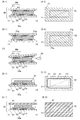
図1(A)は本発明の一態様の発光装置1001の投影図であり、図1(B)は発光装置1001に用いることができる骨格の投影図であり、図1(C)は発光装置1001の構成を説明する組図である。また、図1(D)は図1(C)に示す発光パネル200(1)の切断線X1−X2における断面の構成を説明する断面図である。
1A is a projection view of a light-emitting
<発光装置の構成例1>
本実施の形態で説明する発光装置1001は、骨格100と、骨格100に支持される可撓性の第1の発光パネル200(1)と、骨格100に支持される可撓性の第2の発光パネル200(2)と、を有する(図1(A)参照)。
<Structural example 1 of light emitting device>
The light-emitting
骨格100は、第1の発光パネル200(1)および第2の発光パネル200(2)を支持する湾曲部111、湾曲部111との間に第1の可展面F(1)が形成されるように第1の発光パネル200(1)を支持する第1の直線部101および湾曲部111との間に第2の可展面F(2)が形成されるように第2の発光パネル200(2)を支持する第2の直線部102を備える(図1(B)参照)。
In the
第1の発光パネル200(1)は、第1の発光素子250(1)および第1の発光素子250(1)と電気的に接続する第1の端子部219(1)を備える(図1(C)および図1(D)参照)。 The first light-emitting panel 200 (1) includes a first light-emitting element 250 (1) and a first terminal portion 219 (1) electrically connected to the first light-emitting element 250 (1) (FIG. 1). (C) and FIG. 1 (D)).
第2の発光パネル200(2)は、第2の発光素子250(2)および第2の発光素子250(2)と電気的に接続する第2の端子部219(2)を備える。 The second light-emitting panel 200 (2) includes a second light-emitting element 250 (2) and a second terminal portion 219 (2) that is electrically connected to the second light-emitting element 250 (2).
本実施の形態で説明する発光装置1001は、骨格100と、第1の可展面F(1)が形成されるように骨格100に支持される可撓性の第1の発光パネル200(1)と、第2の可展面F(2)が形成されるように骨格100に支持される可撓性の第2の発光パネル200(2)と、を含んで構成される。
The light-emitting
これにより、第1の発光パネルが形成する第1の可展面、第2の発光パネルが形成する第2の可展面並びに第1の可展面および第2の可展面に挟まれる湾曲した稜線を含む立体を構成できる。その結果、利便性または信頼性に優れた新規な発光装置を提供することができる。 Thereby, the first developable surface formed by the first light-emitting panel, the second developable surface formed by the second light-emitting panel, and a curve sandwiched between the first developable surface and the second developable surface. A solid that includes the ridge line can be constructed. As a result, a novel light-emitting device with high convenience or reliability can be provided.
なお、平面を伸縮することなく変形して得られる曲面を可展面という。可展面は伸縮することなく平面に変形できる。また、可展面にある任意の点を通る直線を当該可展面上に少なくとも一本引くことができる。 Note that a curved surface obtained by deforming a plane without expanding and contracting is referred to as a developable surface. The developable surface can be deformed into a flat surface without stretching. Also, at least one straight line passing through any point on the developable surface can be drawn on the developable surface.
また、発光装置1001は、第2の発光パネル200(2)が、第1の発光パネル200(1)の湾曲部111に支持される一辺S(1)の一部と重ねることができる形状を、湾曲部111に支持される一辺S(2)に備える(図2(B)参照)。
The light-emitting
これにより、第1の発光パネルの一辺および第2の発光パネルの一辺の隙間が狭くなるように、湾曲部が第1の発光パネルおよび第2の発光パネルを支持することができる。その結果、利便性または信頼性に優れた新規な発光装置を提供することができる。 Thus, the curved portion can support the first light emitting panel and the second light emitting panel such that a gap between one side of the first light emitting panel and one side of the second light emitting panel is reduced. As a result, a novel light-emitting device with high convenience or reliability can be provided.
また、第1の発光パネル200(1)は、基材210と、基材270と、基材210および基材270の間の発光素子250(1)と、を備えてもよい(図1(D)参照)。
The first light-emitting panel 200 (1) may include a
また、基材210および基材270を貼り合わせる封止材260を備えてもよい。
Further, a sealing
また、基材210は、バリア膜210aと、基材210bと、バリア膜210aおよび基材210bの間に樹脂層210cと、を備えてもよい。また、基材270は、バリア膜270aと、基材270bと、バリア膜270aおよび基材270bの間に樹脂層270cと、を備えてもよい。
The base 210 may include a
また、発光素子250(1)は、下部電極251と、上部電極252と、下部電極251および上部電極252の間の発光性の有機化合物を含む層253と、を備えてもよい。
Further, the light-emitting element 250 (1) may include a
また、第1の端子部219(1)と、第1の端子部219(1)と発光素子250(1)を電気的に接続する導電層208を備えてもよい。
Further, a first terminal portion 219 (1) and a
また、第3の発光パネル200(3)または第4の発光パネル200(4)を備えてもよい。 Further, a third light-emitting panel 200 (3) or a fourth light-emitting panel 200 (4) may be provided.
以下に、発光装置1001を構成する個々の要素について説明する。なお、これらの構成は明確に分離できず、一つの構成が他の構成を兼ねる場合や他の構成の一部を含む場合がある。
Hereinafter, individual components included in the
《全体の構成》
本発明の一態様の発光装置1001は、骨格100、第1の発光パネル200(1)または第2の発光パネル200(2)を含む。
《Overall configuration》
The light-emitting
《骨格》
骨格100は、第1の直線部101、第2の直線部102または湾曲部111を備える(図1(B)参照)。なお、骨格は、枠、型、フレーム、ワイヤーフレームまたは補強材ともいうことができる。
《Skeleton》
The
また、第1の直線部101、第2の直線部102および湾曲部111は、一の頂点Pが形成されるように端部で接続されてもよい(図1(A)または図2(A)参照)。
Further, the first
また、湾曲部112、湾曲部113および湾曲部114を備えてもよく、第3の直線部103および第4の直線部104を備えてもよい(図1(B)参照)。
Further, a bending
同一の中心を有する一の円弧に沿った形状を、湾曲部111と湾曲部113に用いることができる。また、他の同一の中心を有する他の円弧にそった形状を湾曲部112と湾曲部114に用いることができる。
Shapes along one arc having the same center can be used for the
また、他の円弧が一の円弧の頂点で直交するように配置され、第1の直線部101、第2の直線部102、第3の直線部103および第4の直線部104が正方形またはひし形を描くように配置されてもよい。
Further, the other arcs are arranged so as to be orthogonal to each other at the apex of the one arc, and the first
また、第1の直線部101、第2の直線部102、第3の直線部103および第4の直線部104が長方形を描くように一の円弧を頂点で他の円弧と交差するように配置してもよい。
In addition, one arc is arranged such that the first
第1の直線部101と平行な直線を、第1の可展面F(1)に沿って移動することができる。第1の直線部101は、その表面に含まれる一の接線において第1の可展面F(1)と接する。
A straight line parallel to the first
第2の直線部102と平行な直線を、第2の可展面F(2)に沿って移動することができる。第2の直線部102は、その表面に含まれる一の接線において第2の可展面F(2)と接する。
A straight line parallel to the second
湾曲部111は、その表面に含まれる一の曲線において第1の可展面F(1)と接し、当該一の曲線または他の曲線において第2の可展面F(2)と接する。
The
なお、第1の発光パネル200(1)または第2の発光パネル200(2)は、4mm以上、好ましくは2mm以上、より好ましくは1mm以上の曲率半径を備える曲線において湾曲部111と接する。
Note that the first light-emitting panel 200 (1) or the second light-emitting panel 200 (2) contacts the
例えば、円柱または角柱等の棒状の部材、円筒等の筒状の部材もしくはI字、L字またはV字等の板状の部材等を、第1の直線部101、第2の直線部102または湾曲部111に用いることができる。なお、骨格100は発光パネル200(1)の辺を支持する構成を備えるが、発光パネル200(1)の面を支持する構成を骨格に用いることもできる。開口部を備える骨格は、開口部を備えない骨格より軽量にできる。
For example, a rod-shaped member such as a cylinder or a prism, a cylindrical member such as a cylinder, or a plate-shaped member such as an I-shaped, an L-shaped or a V-shaped, or the like, It can be used for the
例えば、有機材料、無機材料または有機材料と無機材料の複合材料もしくは積層材料を骨格100に用いることができる。具体的には、樹脂、金属、樹脂で被覆された金属、ガラス繊維または炭素繊維が分散された樹脂等を用いることができる。また、木材、紙等の自然素材を用いることもできる。
For example, an organic material, an inorganic material, or a composite material or a laminated material of an organic material and an inorganic material can be used for the
なお、第1の直線部101、第2の直線部102および湾曲部111を接続することができる接続具110を用いてもよい(図2(A)参照)。
Note that a
例えば、第1の直線部101、第2の直線部102および湾曲部111と嵌め合わされて、互いを接続する構造を、接続具110が備えていてもよい。
For example, the
具体的には、外形が他の部分より細い部分が端部に設けられた第1の直線部101、第2の直線部102および湾曲部111と、当該部分と嵌め合わすことができる鞘状の空間が設けられた接続具110と、を用いることができる。
Specifically, a first
《発光パネル》
第1の発光パネル200(1)は、第1の発光素子250(1)、第1の端子部219(1)または可撓性の基材210を備えることができる。
<< Light-emitting panel >>
The first light-emitting panel 200 (1) can include the first light-emitting element 250 (1), the first terminal portion 219 (1), or the
例えば、第1の発光パネル200(1)と同様の構成を、第2の発光パネル200(2)、第3の発光パネル200(3)および第4の発光パネル200(4)に適用できる。 For example, the same configuration as the first light-emitting panel 200 (1) can be applied to the second light-emitting panel 200 (2), the third light-emitting panel 200 (3), and the fourth light-emitting panel 200 (4).
特に、湾曲部111に支持される第2の発光パネル200(2)の一辺S(2)が、第1の発光パネル200(1)の湾曲部111に支持される一辺S(1)の一部と重なる形状を備えると、湾曲部111において第2の発光パネル200(2)を第1の発光パネル200(1)に近接させて配置することができる。例えば、隙間なく配置することができる。
In particular, one side S (2) of the second light emitting panel 200 (2) supported by the
具体的には、一点鎖線で示す一辺S(2)は、第2の発光パネル200(2)を第1の発光パネル200(1)に向かい合わせることにより、一点鎖線で示す一辺S(1)に重ねあわせることができる。言い換えると、第2の発光パネル200(2)の一点鎖線で示す一辺S(2)は、第1の発光パネル200(1)の一点鎖線で示す一辺S(1)と線対称の関係にある形状を備える。 Specifically, one side S (1) indicated by a dashed line is obtained by facing the second light emitting panel 200 (2) to the first light emitting panel 200 (1). Can be superimposed. In other words, the side S (2) indicated by the dashed line of the second light emitting panel 200 (2) is line-symmetric with the side S (1) indicated by the dashed line of the first light emitting panel 200 (1). It has a shape.
線対称の関係にある一点鎖線で示す一辺S(2)を一点鎖線で示す一辺S(1)に沿わせて配置すると、第2の発光パネル200(2)を第1の発光パネル200(1)に近接させることができる。例えば、第2の発光パネル200(2)と第1の発光パネル200(1)とで、稜線を形成することができる。 When the side S (2) indicated by the dashed line and the line symmetrical relationship are arranged along the side S (1) indicated by the dashed line, the second light emitting panel 200 (2) is changed to the first light emitting panel 200 (1). ). For example, a ridge line can be formed by the second light-emitting panel 200 (2) and the first light-emitting panel 200 (1).
また、第1の発光パネル200(1)乃至第4の発光パネル200(4)は光を少なくとも一方の側に射出する。例えば、発光装置1001が備える第1の発光パネル200(1)乃至第4の発光パネル200(4)は、いずれも形成される可展面の凸の側に光を射出してもよい。なお、第2の発光パネル200(2)が光を射出する方向を矢印で図中に示す(図1(A)参照)。
The first to fourth light-emitting panels 200 (1) to 200 (4) emit light to at least one side. For example, the first light-emitting panel 200 (1) to the fourth light-emitting panel 200 (4) included in the light-emitting
なお、第1の発光パネルまたは第2の発光パネルが形成する曲面は、4mm以上、好ましくは2mm以上、より好ましくは1mm以上の曲率半径を備える。 Note that a curved surface formed by the first light-emitting panel or the second light-emitting panel has a radius of curvature of 4 mm or more, preferably 2 mm or more, more preferably 1 mm or more.
なお、発光パネル200(1)の外形は特に限定されない。例えば、一の角で交わる曲線状の二つの辺と、一の角と対向する直線状の辺と、を有する略三角形の外形言い換えると船形の外形を、発光パネルの外形に適用できる。また、端子部219(1)は、直線状の辺に設けられる。 The outer shape of the light emitting panel 200 (1) is not particularly limited. For example, a substantially triangular outer shape having two curved sides intersecting at one corner and a straight side facing the one corner, in other words, a boat-shaped outer shape can be applied to the outer shape of the light emitting panel. The terminal portion 219 (1) is provided on a straight side.
《発光素子》
さまざまな発光素子を第1の発光素子250(1)に適用できる。例えば、有機エレクトロルミネッセンスまたは無機エレクトロルミネッセンスを利用する発光素子、発光ダイオード等を用いることができる。
《Light emitting element》
Various light-emitting elements can be applied to the first light-emitting element 250 (1). For example, a light-emitting element, a light-emitting diode, or the like utilizing organic electroluminescence or inorganic electroluminescence can be used.
具体的には、下部電極251と下部電極251に重なる上部電極252と、下部電極251および上部電極252に挟持される発光性の有機化合物を含む層253と、を備える発光素子(有機EL素子ともいう)を第1の発光素子250(1)に用いることができる(図1(D)参照)。
Specifically, a light-emitting element (including an organic EL element) including a
なお、第1の発光パネル200(1)は、光を上部電極252側または/および下部電極251側に射出してもよい。第1の発光パネル200(1)が光を上部電極252側に射出する例を図中に矢印で示す(図1(D)参照)。
Note that the first light-emitting panel 200 (1) may emit light to the
《導電層および端子部》
導電層208は、発光素子250(1)と電気的に接続されている。
《Conductive layer and terminal section》
The
端子部219(1)は信号または電力等を供給される。導電層208の一部が端子部219(1)に設けられる。例えば、フレキシブルプリント基板と端子部219(1)を電気的に接続することができるように、端子部219(1)の一部に導電層208の一部を露出させてもよい。
The terminal portion 219 (1) is supplied with a signal, power, or the like. Part of the
導電性を有する材料を導電層208に用いることができる。
A conductive material can be used for the
具体的には、アルミニウム、金、白金、銀、銅、クロム、タンタル、チタン、モリブデン、タングステン、ニッケル、鉄、コバルト、パラジウムまたはマンガンから選ばれた金属元素などを、用いることができる。または、上述した金属元素を含む合金などを、用いることができる。特に、銅とマンガンの合金がウエットエッチング法を用いた微細加工に好適である。 Specifically, a metal element selected from aluminum, gold, platinum, silver, copper, chromium, tantalum, titanium, molybdenum, tungsten, nickel, iron, cobalt, palladium, or manganese can be used. Alternatively, an alloy containing the above-described metal element or the like can be used. In particular, an alloy of copper and manganese is suitable for fine processing using a wet etching method.
具体的には、アルミニウム膜上にチタン膜を積層する二層構造、窒化チタン膜上にチタン膜を積層する二層構造、窒化チタン膜上にタングステン膜を積層する二層構造、窒化タンタル膜または窒化タングステン膜上にタングステン膜を積層する二層構造、チタン膜と、そのチタン膜上にアルミニウム膜を積層し、さらにその上にチタン膜を形成する三層構造等を用いることができる。 Specifically, a two-layer structure in which a titanium film is stacked over an aluminum film, a two-layer structure in which a titanium film is stacked over a titanium nitride film, a two-layer structure in which a tungsten film is stacked over a titanium nitride film, a tantalum nitride film, or A two-layer structure in which a tungsten film is stacked over a tungsten nitride film, a three-layer structure in which a titanium film, an aluminum film is stacked over the titanium film, and a titanium film is further formed thereon can be used.
具体的には、アルミニウムに、チタン、タンタル、タングステン、モリブデン、クロム、ネオジム、スカンジウムから選ばれた一または複数を組み合わせた合金膜、もしくは窒化膜を用いてもよい。 Specifically, an alloy film or a nitride film in which one or more selected from titanium, tantalum, tungsten, molybdenum, chromium, neodymium, and scandium are combined with aluminum may be used.
また、導電性を備える金属酸化物等を含む導電性の材料を用いてもよい。具体的には酸化インジウム、酸化錫または酸化亜鉛等を用いてもよい。 Alternatively, a conductive material including a metal oxide or the like having conductivity may be used. Specifically, indium oxide, tin oxide, zinc oxide, or the like may be used.
《基材》
有機材料、無機材料または有機材料と無機材料の複合材料を可撓性の基材210に用いることができる。なお、基材210に用いることができる材料を基材270に用いることができる。
"Base material"
An organic material, an inorganic material, or a composite material of an organic material and an inorganic material can be used for the
5μm以上2500μm以下、好ましくは5μm以上680μm以下、より好ましくは5μm以上170μm以下、より好ましくは5μm以上45μm以下、より好ましくは8μm以上25μm以下の厚さを有する材料を、基材210に用いることができる。
A material having a thickness of 5 μm or more and 2500 μm or less, preferably 5 μm or more and 680 μm or less, more preferably 5 μm or more and 170 μm or less, more preferably 5 μm or more and 45 μm or less, more preferably 8 μm or more and 25 μm or less is used for the
また、不純物の透過が抑制された材料を基材210に好適に用いることができる。例えば、水蒸気の透過率が10−5g/(m2・day)以下、好ましくは10−6g/(m2・day)以下である材料を好適に用いることができる。
In addition, a material in which transmission of impurities is suppressed can be suitably used for the
また、複数の材料が積層された材料を用いる場合は、互いに線膨張率がおよそ等しい材料を基材210に好適に用いることができる。例えば、線膨張率が1×10⁻³/K以下、好ましくは5×10−5/K以下、より好ましくは1×10−5/K以下である材料を好適に用いることができる。
In the case where a material in which a plurality of materials are stacked is used, materials having approximately equal linear expansion coefficients can be suitably used for the
例えば、樹脂、樹脂フィルムまたはプラスチックフィルム等の有機材料を、基材210に用いることができる。
For example, an organic material such as a resin, a resin film, or a plastic film can be used for the
例えば、金属板または厚さ10μm以上50μm以下の薄板状のガラス板等の無機材料を、基材210に用いることができる。
For example, an inorganic material such as a metal plate or a thin glass plate having a thickness of 10 μm to 50 μm can be used for the
例えば、金属板、薄板状のガラス板または無機材料の膜を、樹脂層を用いて樹脂フィルム等に貼り合せて形成された複合材料を、基材210に用いることができる。
For example, a composite material formed by bonding a metal plate, a thin glass plate, or a film of an inorganic material to a resin film or the like using a resin layer can be used for the
例えば、繊維状または粒子状の金属、ガラスもしくは無機材料を樹脂または樹脂フィルムに分散した複合材料を、基材210に用いることができる。
For example, a composite material in which fibrous or particulate metal, glass, or an inorganic material is dispersed in a resin or a resin film can be used for the
例えば、熱硬化性樹脂や紫外線硬化樹脂を樹脂層に用いることができる。 For example, a thermosetting resin or an ultraviolet curable resin can be used for the resin layer.
具体的には、ポリエステル、ポリオレフィン、ポリアミド、ポリイミド、ポリカーボネート若しくはアクリル樹脂等の樹脂フィルムまたは樹脂板を用いることができる。 Specifically, a resin film or a resin plate of polyester, polyolefin, polyamide, polyimide, polycarbonate, acrylic resin, or the like can be used.
具体的には、無アルカリガラス、ソーダ石灰ガラス、カリガラス若しくはクリスタルガラス等を用いることができる。 Specifically, non-alkali glass, soda-lime glass, potash glass, crystal glass, or the like can be used.
具体的には、金属酸化物膜、金属窒化物膜若しくは金属酸窒化物膜等を用いることができる。例えば、酸化珪素、窒化珪素、酸窒化珪素、アルミナ膜等を適用できる。 Specifically, a metal oxide film, a metal nitride film, a metal oxynitride film, or the like can be used. For example, silicon oxide, silicon nitride, silicon oxynitride, an alumina film, or the like can be used.
具体的には、開口部が設けられたSUSまたはアルミニウム等を用いることができる。 Specifically, SUS or aluminum provided with an opening can be used.
具体的には、アクリル、ウレタン、エポキシ、またはシロキサン結合を有する樹脂などの樹脂を用いることができる。 Specifically, a resin such as acrylic, urethane, epoxy, or a resin having a siloxane bond can be used.
例えば、可撓性を有する基材210bと、不純物の拡散を防ぐバリア膜210aと、基材210bおよびバリア膜210aを貼り合わせる樹脂層210cと、が積層された積層体を基材210に好適に用いることができる(図1(D)参照)。
For example, a laminate in which a
具体的には、600nmの酸化窒化珪素膜および厚さ200nmの窒化珪素膜が積層された積層材料を含む膜を、バリア膜210aに用いることができる。
Specifically, a film including a stacked material in which a 600-nm-thick silicon oxynitride film and a 200-nm-thick silicon nitride film are stacked can be used for the
具体的には、厚さ600nmの酸化窒化珪素膜、厚さ200nmの窒化珪素膜、厚さ200nmの酸化窒化珪素膜、厚さ140nmの窒化酸化珪素膜および厚さ100nmの酸化窒化珪素膜がこの順に積層された積層材料を含む膜を、バリア膜210aに用いることができる。
Specifically, a silicon oxynitride film having a thickness of 600 nm, a silicon nitride film having a thickness of 200 nm, a silicon oxynitride film having a thickness of 200 nm, a silicon oxynitride film having a thickness of 140 nm, and a silicon oxynitride film having a thickness of 100 nm are provided. A film including a stacked material that is sequentially stacked can be used for the
具体的には、ポリエステル、ポリオレフィン、ポリアミド、ポリイミド、ポリカーボネート若しくはアクリル樹脂等の樹脂フィルム、樹脂板または積層体等を基材210bに用いることができる。
Specifically, a resin film such as polyester, polyolefin, polyamide, polyimide, polycarbonate, or acrylic resin, a resin plate, a laminate, or the like can be used for the
具体的には、ポリエステル、ポリオレフィン、ポリアミド(ナイロン、アラミド等)、ポリイミド、ポリカーボネートまたはアクリル、ウレタン、エポキシもしくはシロキサン結合を有する樹脂を含む材料を樹脂層210cに用いることができる。
Specifically, a material containing a resin having polyester, polyolefin, polyamide (eg, nylon, aramid), polyimide, polycarbonate, or acrylic, urethane, epoxy, or siloxane bond can be used for the
<発光装置の構成例2.>
本発明の一態様の発光装置の別の構成について、図3を参照しながら説明する。
<Structural example of light emitting device 2. >
Another structure of the light-emitting device of one embodiment of the present invention will be described with reference to FIGS.
図3は本発明の一態様の発光装置1001Bの構成を説明する図である。
FIG. 3 illustrates a structure of a light-emitting
図3(A)は本発明の一態様の発光装置1001Bの投影図であり、図3(B)は図3(A)に示す発光装置1001Bを90°右に回転し且つ構成の一部が省略された投影図である。また、図3(C−1)は、図3(A)に示す発光装置1001Bの切断線X3−X4における断面の構成および内部の構造を説明する側面図であり、図3(C−2)は、一部の構成が省略された発光装置1001Bの側面図である。
FIG. 3A is a projection view of the light-emitting
本実施の形態で説明する発光装置1001Bは、第1の発光パネル200(1)が、第1の直線部101の外形に沿うように曲げられた領域を、第1の発光素子および第1の端子部219(1)の間に備える(図3(A)乃至図3(C−2)参照)。
In the light-emitting
これにより、第1の端子部を第1の直線部の外形に沿わせながら折り曲げることができる。その結果、利便性または信頼性に優れた新規な発光装置を提供することができる。 Thereby, the first terminal portion can be bent while being along the outer shape of the first linear portion. As a result, a novel light-emitting device with high convenience or reliability can be provided.
なお、第2の発光パネル200(2)が光を射出する方向を矢印で図中に示す(図3(A)参照)。 Note that the direction in which the second light-emitting panel 200 (2) emits light is indicated by an arrow in the drawing (see FIG. 3A).
また、発光装置1001Bは、第1の端子部219(1)が第1の直線部101の外形に沿って曲げられて配置されている点が、図1を参照しながら説明する発光装置1001とは異なる(図1(A)および図3(B)参照)。ここでは異なる構成について詳細に説明し、同様の構成を用いることができる部分は、上記の説明を援用する。
The
《全体の構成》
本発明の一態様の発光装置1001Bは、骨格100、第1の発光パネル200(1)または第2の発光パネル200(2)を含む。
《Overall configuration》
A light-emitting
《第1の端子部》
第1の端子部219(1)は可撓性を有する。
<< First terminal section >>
The first terminal portion 219 (1) has flexibility.
例えば、可撓性を有する基材210の一部が第1の端子部219(1)を支持する構成にしてもよい。
For example, a configuration may be employed in which a part of the
可撓性を有する第1の端子部219(1)は、第1の直線部101の外形に沿って折り曲げることができる。
The first terminal portion 219 (1) having flexibility can be bent along the outer shape of the first
《骨格》
第1の直線部101は、第1の端子部219(1)を壊すことなく曲げて沿わせることができる外形を備える。
《Skeleton》
The first
例えば、第1の端子部219(1)を壊すことなく曲げて沿わせることができる曲率を有する曲面を備える。 For example, it has a curved surface having a curvature that can be bent along the first terminal portion 219 (1) without breaking.
具体的には、断面の形状が円形である材料を、第1の直線部101に用いることができる(図3(C−1)参照)。 Specifically, a material having a circular cross section can be used for the first straight portion 101 (see FIG. 3C-1).
なお、第1の発光パネルまたは第2の発光パネルが接する曲面は、4mm以上、好ましくは2mm以上、より好ましくは1mm以上の曲率半径を備える。 Note that the curved surface with which the first light emitting panel or the second light emitting panel is in contact has a radius of curvature of 4 mm or more, preferably 2 mm or more, more preferably 1 mm or more.
<発光装置の構成例3.>
本発明の一態様の発光装置の別の構成について、図4を参照しながら説明する。
<Structural example 3 of light emitting device>>
Another structure of the light-emitting device of one embodiment of the present invention will be described with reference to FIGS.
図4は本発明の一態様の発光装置1001Cの構成を説明する図である。
FIG. 4 illustrates a structure of a light-emitting
図4(A)は本発明の一態様の発光装置1001Cの投影図であり、図4(B)は、発光装置1001Cの一部の構成が省略された投影図である。
FIG. 4A is a projection view of a light-emitting
本実施の形態で説明する発光装置1001Cは、湾曲部111Cが第1の発光パネル200C(1)と重なる領域を備え、第1の発光パネル200C(1)が、光を湾曲部111Cが配置されていない側に向けて射出する(図4(A)および図4(B)参照)。なお、第1の発光パネル200C(1)は、第1の端子部219C(1)を備える。
The light-emitting
これにより、第1の発光パネルは湾曲部にさえぎられることなく光を射出することができる。その結果、利便性または信頼性に優れた新規な発光装置を提供することができる。 Thus, the first light emitting panel can emit light without being interrupted by the curved portion. As a result, a novel light-emitting device with high convenience or reliability can be provided.
また、第1の発光パネル200C(1)乃至第4の発光パネル200C(4)が、凹状の可展面を形成し且つ当該凹状の可展面が光を射出するように配置されている点が、図1を参照しながら説明する発光装置1001とは異なる(図1(A)参照)。ここでは異なる構成について詳細に説明し、同様の構成を用いることができる部分は、上記の説明を援用する。
In addition, the first light-emitting
《骨格》
骨格100Cは、第1の直線部101C、第2の直線部102Cまたは湾曲部111Cを備える(図4(B)参照)。
《Skeleton》
The
また、第1の直線部101C、第2の直線部102Cおよび湾曲部111Cは、一の頂点Pが形成されるように端部で接続されてもよい(図4(A)参照)。
Further, the first
《発光パネル》
発光パネル200C(1)および発光パネル200C(2)は湾曲部111Cの凹状に湾曲する側に配置される。
<< Light-emitting panel >>
The
また、第1の発光パネル200C(1)乃至第4の発光パネル200C(4)は、凹状の可展面が形成され、且つ当該凹状の可展面が形成された側に光を射出するように配置される。
Each of the first to fourth light-emitting
なお、第3の発光パネル200C(3)が光を射出する方向を図中に矢印で示す(図4(B)参照)。
The direction in which the third light-emitting
なお、本実施の形態は、本明細書で示す他の実施の形態と適宜組み合わせることができる。 Note that this embodiment can be combined with any of the other embodiments in this specification as appropriate.
(実施の形態2)
本実施の形態では、本発明の一態様の表示装置の構成について、図5を参照しながら説明する。
(Embodiment 2)
In this embodiment, a structure of a display device of one embodiment of the present invention will be described with reference to FIGS.
図5は本発明の一態様の発光装置1001Dの構成を説明する図である。
FIG. 5 illustrates a structure of a light-emitting
図5(A)は本発明の一態様の発光装置1001Dの投影図であり、図5(B)は図5(A)に示す発光装置1001Dに用いることができる骨格100Dの投影図であり、図5(C)は図5(A)に示す発光装置1001Dを90°右に回転し且つ構成の一部が省略された投影図である。また、図5(D)は図5(A)に示す発光装置1001Dの切断線X5−X6における断面の構成および内部の構造を説明する側面図である。
FIG. 5A is a projection view of a light-emitting
<発光装置の構成例4>
本実施の形態で説明する発光装置1001Dは、骨格100Dと、骨格100Dに支持される可撓性の第1の発光パネル200D(1)と、骨格100Dに支持される可撓性の第2の発光パネル200D(2)と、を有する(図5(A)および図5(B)参照)。
<Structural example 4 of light emitting device>
A light-emitting
そして、骨格100Dは、第1の発光パネル200D(1)を支持する第1の湾曲部111D、第1の湾曲部111Dとの間に第1の可展面F(1)が形成されるように第1の発光パネル200D(1)を支持する第1の直線部101D、第1の直線部101Dに対向する第2の直線部102Dおよび第2の直線部102Dとの間に第2の可展面F(2)が形成されるように第2の発光パネル200D(2)を支持する第2の湾曲部112Dを備える。
Then, in the
第1の発光パネル200D(1)は、第1の発光素子250D(1)、第1の発光素子250D(1)と電気的に接続する第1の端子部219D(1)および第1の直線部101Dの外形に沿うように曲げられた領域を第1の発光素子250D(1)と第1の端子部219D(1)の間に備える(図5(A)および図5(C)参照)。
The first light-emitting
第2の発光パネル200D(2)は、第2の発光素子250D(2)、第2の発光素子250D(2)と電気的に接続する第2の端子部219D(2)および第2の直線部102Dの外形に沿うように曲げられた領域を第2の発光素子250D(2)と第2の端子部219D(2)の間に備える(図5(C)参照)。
The second light-emitting
上記本発明の一態様の発光装置1001Dは、第1の湾曲部111Dならびに第1の直線部101Dおよび第2の直線部102Dを備える骨格100Dと、第1の可展面F(1)が形成されるように骨格100Dに支持される可撓性の第1の発光パネル200D(1)と、第2の可展面F(2)が形成されるように第1の直線部101Dに対向する第2の直線部102Dに支持される可撓性の第2の発光パネル200D(2)と、を含んで構成される。そして、第1の発光パネル200D(1)が備える第1の端子部219D(1)および第2の発光パネル200D(2)が備える第2の端子部219D(2)が、第1の直線部101Dおよび第2の直線部102Dの外形に沿って曲げられる。
The light-emitting
これにより、第1の発光パネルが形成する湾曲した第1の可展面と、第1の発光パネルを支持する第1の直線部と対向する第2の直線部に支持される第2の発光パネルが形成する第2の可展面と、を含む立体を構成することができる。また、第1の発光パネルの第1の端子部および第2の発光パネルの第2の端子部を第1の直線部および第2の直線部の間から取り出すことができる。その結果、利便性または信頼性に優れた新規な発光装置を提供することができる。 Accordingly, the curved first developable surface formed by the first light-emitting panel and the second light emission supported by the second linear portion facing the first linear portion supporting the first light-emitting panel. A three-dimensional structure including the second developable surface formed by the panel can be configured. Further, the first terminal portion of the first light-emitting panel and the second terminal portion of the second light-emitting panel can be taken out from between the first straight portion and the second straight portion. As a result, a novel light-emitting device with high convenience or reliability can be provided.
また、第3の発光パネル200D(3)乃至第8の発光パネル200D(8)を備えてもよい。
Further, a third light-emitting
以下に、発光装置1001Dを構成する個々の要素について説明する。なお、これらの構成は明確に分離できず、一つの構成が他の構成を兼ねる場合や他の構成の一部を含む場合がある。
Hereinafter, individual components included in the
また、発光装置1001Dは、骨格100Dが第1の直線部101Dに対向する第2の直線部102Dを備える点、第2の発光パネル200D(2)が湾曲部111に支持されていない点および第1の端子部219D(1)および第2の端子部219D(2)が、第1の直線部101Dおよび第2の直線部102Dの外形に沿って曲げられる点が、図3を参照しながら説明する発光装置1001Bとは異なる(図3(B)参照)。ここでは異なる構成について詳細に説明し、同様の構成を用いることができる部分は、実施の形態1に記載された説明を援用する。
Further, the
《全体の構成》
本発明の一態様の発光装置1001Dは、骨格100D、第1の発光パネル200D(1)または第2の発光パネル200D(2)を含む。
《Overall configuration》
A light-emitting
《骨格》
骨格100Dは、第1の直線部101D、第2の直線部102Dまたは湾曲部111Dを備える(図5(B)参照)。
《Skeleton》
The
なお、本実施の形態で例示する骨格100Dの形状は、実施の形態1で例示して説明する2つの骨格100の直線部が対向するように配置された形状ということができる。
Note that the shape of the
骨格100Dは、多角形の断面と円弧を含む断面を備える多様な立体を提供できる。
The
また、第1の直線部101D、第2の直線部102Dおよび湾曲部111Dは、一の頂点Pが形成されるように端部で接続されてもよい。
Further, the first
また、第3の直線部103D乃至第8の直線部108Dを備えてもよい。
Further, a third
また、第2の湾曲部112D乃至第8の湾曲部118Dを備えてもよい。
Further, a
一の円弧に沿った形状を、湾曲部111D、湾曲部112D、湾曲部116Dおよび湾曲部115Dに用いることができる。また、他の円弧にそった形状を湾曲部113D、湾曲部114D、湾曲部118Dおよび湾曲部117Dに用いることができる。
A shape along one arc can be used for the bending
また、他の円弧が一の円弧の頂点で直交するように配置され、第1の直線部101D、第3の直線部103D、第5の直線部105Dおよび第7の直線部107Dが正方形またはひし形を描くように配置されてもよく、第2の直線部102D、第4の直線部104D、第6の直線部106Dおよび第8の直線部108Dが正方形またはひし形を描くように配置されてもよい。
The other arcs are arranged so as to be orthogonal to each other at the apex of the one arc, and the first
また、第1の直線部101D、第3の直線部103D、第5の直線部105Dおよび第7の直線部107Dが長方形を描くように、他の円弧と一の円弧を頂点で交差させて配置してもよく、第2の直線部102D、第4の直線部104D、第6の直線部106Dおよび第8の直線部108Dが長方形を描くように、他の円弧と一の円弧を頂点で交差させて配置してもよい。
In addition, the first
第2の直線部102Dは第1の直線部101Dに対向し、第1の直線部101Dと第2の直線部102Dの間には、第1の端子部219D(1)および第2の端子部219D(2)を配置することができる。
The second
《発光パネル》
第1の発光パネル200D(1)は、湾曲部111Dと第1の直線部101Dの間に可展面F(1)が形成されるように支持され、第1の直線部101Dの外形に沿って第1の端子部219D(1)が配置される(図5(C)参照)。
<< Light-emitting panel >>
The first light-emitting
また、第1の直線部101Dは、その表面に含まれる一の接線において第1の発光パネル200D(1)と接する。
In addition, the first
第2の発光パネル200D(2)は、湾曲部112Dと第2の直線部102Dの間に可展面F(2)が形成されるように支持され、第2の直線部102Dの外形に沿って第2の端子部219D(2)が配置される。
The second light-emitting
また、第2の直線部102Dは、その表面に含まれる一の接線において第2発光パネル200D(2)と接する。
In addition, the second
言い換えると、第1の端子部219D(1)および第2の端子部219D(2)は、第1の直線部101Dおよび第2の直線部102Dの間を通って且つそれぞれの外形に沿って配置される(図5(C)参照)。
In other words, the
なお、第2の直線部102Dが第2の発光パネル200D(2)に接する接線は、第1の直線部101Dが第1の発光パネル200D(1)に接する接線とおよそ平行である。
The tangent line at which the second
また、発光装置1001Dは、第3の発光パネル200D(3)乃至第8の発光パネル200D(8)を備えてもよい。
Further, the light-emitting
例えば、実施の形態1で説明する発光パネルと同様の構成を、第1の発光パネル200D(1)乃至第8の発光パネル200D(8)に適用できる。
For example, a structure similar to that of the light-emitting panel described in
なお、第3の発光パネル200D(3)が光を射出する方向を矢印で図中に示す(図5(A)参照)。
The direction in which the third light-emitting
なお、本実施の形態は、本明細書で示す他の実施の形態と適宜組み合わせることができる。 Note that this embodiment can be combined with any of the other embodiments in this specification as appropriate.
(実施の形態3)
本実施の形態では、本発明の一態様の表示装置の構成について、図6を参照しながら説明する。
(Embodiment 3)
In this embodiment, a structure of a display device of one embodiment of the present invention will be described with reference to FIGS.
図6は本発明の一態様の表示装置1002の構成を説明する図である。図6(A)は本発明の一態様の表示装置1002の斜め上方からの投影図であり、図6(B)は図6(A)に示す表示装置1002の斜め下方からの投影図である。
FIG. 6 illustrates a structure of a
<表示装置の構成例1.>
本実施の形態で説明する表示装置1002は、骨格100Eと、骨格100Eに支持される可撓性の第1の表示パネル300(1)と、骨格100Eに支持される可撓性の第2の表示パネル300(2)と、を有する(図6(A)参照)。
<Structural Example of Display Device 1. >
The
そして、骨格100Eは、第1の表示パネル300(1)および第2の表示パネル300(2)を支持する湾曲部111E、湾曲部111Eとの間に第1の可展面が形成されるように第1の表示パネル300(1)を支持する第1の直線部101Eおよび湾曲部111Eとの間に第2の可展面が形成されるように第2の表示パネル300(2)を支持する第2の直線部102Eを備える。
In the
第1の表示パネル300(1)は、第1の発光素子および第1の発光素子と電気的に接続する第1の端子部319(1)および第1の直線部101Eの外形に沿うように曲げられた領域を第1の発光素子と第1の端子部319(1)の間に備える。
The first display panel 300 (1) extends along the outer shape of the first light emitting element and the first terminal portion 319 (1) electrically connected to the first light emitting element and the first
第2の表示パネル300(2)は、第2の発光素子および第2の発光素子と電気的に接続する第2の端子部319(2)および第2の直線部102Eの外形に沿うように曲げられた領域を第2の発光素子と第2の端子部319(2)の間に備える。
The second display panel 300 (2) is formed along the outer shape of the second light emitting element and the second terminal portion 319 (2) electrically connected to the second light emitting element and the second
本実施の形態で説明する表示装置1002は、骨格100Eと、第1の可展面が形成されるように骨格100Eに支持される可撓性の第1の表示パネル300(1)と、第2の可展面が形成されるように骨格100Eに支持される可撓性の第2の表示パネル300(2)と、を含んで構成される。
The
これにより、第1の表示パネルが形成する第1の可展面、第2の表示パネルが形成する第2の可展面並びに第1の可展面および第2の可展面に挟まれる湾曲した稜線を含む立体を構成できる。その結果、利便性または信頼性に優れた新規な表示装置を提供することができる。例えば、全天周映像等を表示する表示装置またはプラネタリウム等に用いることができる。 Thereby, the first developable surface formed by the first display panel, the second developable surface formed by the second display panel, and the curve sandwiched between the first developable surface and the second developable surface. A solid that includes the ridge line can be constructed. As a result, a novel display device with excellent convenience or reliability can be provided. For example, it can be used for a display device that displays an all-sky image or the like, a planetarium, or the like.
《全体の構成》
本発明の一態様の表示装置1002は、骨格100E、第1の表示パネル300(1)または第2の表示パネル300(2)を有する。
《Overall configuration》
The
《骨格》
骨格100Eは、湾曲部111E、第1の直線部101Eまたは第2の直線部102Eを備える。
《Skeleton》
The
骨格100Eは、12の湾曲部または12の直線部を備えてもよい。
The
骨格100Eは、一の円弧に沿った形状を備える2つの湾曲部を含む一組の湾曲部を6組有してもよい。
The
骨格100Eに代えて、複数の湾曲部が交差する部分に支柱を備える骨格を用いることができる。例えば、湾曲部が凹状に湾曲する側に延びる支柱を備える、こうもり傘の骨格のような骨格を用いてもよい。また、表示パネル300(1)を駆動する駆動装置または電源を支柱に配設し、配線を湾曲部に沿って配設してもよい。駆動装置または電源および表示パネル300(1)の端子部319(1)を配線と電気的に接続してもよい。これにより、表示パネル300(1)を支柱に配設された駆動装置または電源を用いて動作することができる。
Instead of the
《表示パネル》
第1の表示パネル300(1)は発光素子および発光素子と電気的に接続する第1の端子部319(1)を備え、可撓性を有する。
《Display panel》
The first display panel 300 (1) includes a light-emitting element and a first terminal portion 319 (1) electrically connected to the light-emitting element, and has flexibility.
第2の表示パネル300(2)は発光素子および発光素子と電気的に接続する第2の端子部319(2)を備え、可撓性を有する。 The second display panel 300 (2) includes a light-emitting element and a second terminal portion 319 (2) that is electrically connected to the light-emitting element, and has flexibility.
第1の端子部319(1)は第1の直線部101Eの外形に沿って配置され、第2の端子部319(2)は第2の直線部102Eの外形に沿って配置される。
The first terminal portion 319 (1) is arranged along the outer shape of the first
第1の端子部319(1)は第1の画像情報を供給され、第1の表示パネル300(1)は第1の画像情報を表示する。 The first terminal portion 319 (1) is supplied with the first image information, and the first display panel 300 (1) displays the first image information.
第2の端子部319(2)は第2の画像情報を供給され、第2の表示パネル300(2)は第2の画像情報を表示する。 The second terminal portion 319 (2) is supplied with the second image information, and the second display panel 300 (2) displays the second image information.
凹状の可展面が形成される側に第1の画像情報が表示されるように、第1の表示パネル300(1)を骨格100Eに支持させる(図6(B)参照)。
The first display panel 300 (1) is supported by the
凹状の可展面が形成される側に第2の画像情報が表示されるように第2の表示パネル300(2)を骨格100Eに支持させる。
The second display panel 300 (2) is supported by the
なお、湾曲部111E、すなわち第2の表示パネル300(2)が形成する第2の可展面の、第1の表示パネル300(1)が形成する第1の可展面に隣接する部分に、第1の表示パネル300(1)に表示される画像とつながる画像が表示されるように、第1の表示パネル300(1)に第1の画像情報を供給し、第2の表示パネル300(2)に第1の画像情報に関連付けられた第2の画像情報を供給してもよい。
Note that the
これにより、例えば、複数の表示パネルで構成された凹状の曲面に、つなげられた画像を使用者が一つの画像と認識するように表示することができる。 Thus, for example, a connected image can be displayed on a concave curved surface formed by a plurality of display panels so that the user recognizes the image as one image.
具体的には、表示装置1002の大きさを、表示装置1002の使用者の顔面を覆う程度のボウル状の大きさまたは使用者が内部に入れる程度のドーム状の大きさにすることにより、使用者が豊かな臨場感を覚える画像を表示することができる。
Specifically, the size of the
また、投影機を用いる方法に比べて高い輝度で画像を表示することができる。また、投影機を用いる方法に比べて高い精細度の画像を表示することができる。 In addition, an image can be displayed with higher luminance than a method using a projector. Further, an image with higher definition can be displayed as compared with a method using a projector.
具体的には、直径20cm以上、直径1m以上、直径2m以上、直径5m以上、直径10m以上、直径20m以上、直径30m以上250m以下が好ましい。 Specifically, the diameter is preferably at least 20 cm, at least 1 m, at least 2 m, at least 5 m, at least 10 m, at least 20 m, at least 30 m and at most 250 m.
なお、第1の表示パネル300(1)または第2の表示パネル300(2)に用いることができる表示パネルの構成の一例を、実施の形態5で詳細に説明する。
Note that an example of a structure of a display panel that can be used for the first display panel 300 (1) or the second display panel 300 (2) is described in
なお、本実施の形態は、本明細書で示す他の実施の形態と適宜組み合わせることができる。 Note that this embodiment can be combined with any of the other embodiments in this specification as appropriate.
(実施の形態4)
本実施の形態では、本発明の一態様の入出力装置の構成について、図7を参照しながら説明する。
(Embodiment 4)
In this embodiment, a structure of the input / output device of one embodiment of the present invention will be described with reference to FIGS.
図7は本発明の一態様の入出力装置1003の構成を説明する図である。
FIG. 7 illustrates a structure of the input /
図7(A)は本発明の一態様の入出力装置1003の斜め上方からの投影図であり、図7(B)は図7(A)に示す入出力装置1003の構成の一部が省略された投影図であり、図7(C)は図7(A)に示す入出力装置1003に用いることができる骨格100Fの投影図であり、図7(D)は図7(A)に示す切断線X7−X8における断面の構造および内部の構造を説明する側面図である。
FIG. 7A is a perspective view of the input /
<入出力装置の構成例>
本実施の形態で説明する入出力装置1003は、骨格100Fと、骨格100Fに支持される可撓性の第1のタッチパネル500(1)と、骨格100Fに支持される可撓性の第2のタッチパネル500(2)と、を有する(図7(A)および図7(C)参照)。
<Example of configuration of input / output device>
The input /
そして、骨格100Fは、第1のタッチパネル500(1)を支持する第1の湾曲部111F、第1の湾曲部111Fとの間に第1の可展面が形成されるように第1のタッチパネル500(1)を支持する第1の直線部101F、第1の直線部101Fに対向する第2の直線部102Fおよび第2の直線部102Fとの間に第2の可展面が形成されるように第2のタッチパネル500(2)を支持する第2の湾曲部を備える(図7(A)および図7(C)参照)。
The
第1のタッチパネル500(1)は、第1の発光素子、第1の発光素子と電気的に接続する第1の端子部519(1)および第1の直線部101Fの外形に沿うように曲げられた領域を第1の発光素子と第1の端子部519(1)の間に備える(図7(D)参照)。
The first touch panel 500 (1) is bent along the outer shape of the first light emitting element, the first terminal portion 519 (1) electrically connected to the first light emitting element, and the first
第2のタッチパネル500(2)は、第2の発光素子、第2の発光素子と電気的に接続する第2の端子部519(2)および第2の直線部102Fの外形に沿うように曲げられた領域を第2の発光素子と第2の端子部519(2)の間に備える。
The second touch panel 500 (2) is bent along the outer shape of the second light emitting element, the second terminal portion 519 (2) electrically connected to the second light emitting element, and the second
上記本発明の一態様の入出力装置1003は、第1の湾曲部111Fならびに第1の直線部101Fおよび第2の直線部102Fを備える骨格100Fと、第1の可展面が形成されるように骨格100Fに支持される可撓性の第1のタッチパネル500(1)と、第2の可展面が形成されるように第1の直線部101Fに対向する第2の直線部102Fに支持される可撓性の第2のタッチパネル500(2)と、を含んで構成される。そして、第1のタッチパネル500(1)が備える第1の端子部519(1)および第2のタッチパネル500(2)が備える第2の端子部519(2)が、第1の直線部101Fおよび第2の直線部102Fの外形に沿って曲げられる。
In the input /
これにより、第1のタッチパネルが形成する湾曲した第1の可展面と、第1のタッチパネルを支持する第1の直線部と対向する第2の直線部に支持される第2のタッチパネルが形成する第2の可展面と、を含む立体を構成することができる。また、第1のタッチパネルの第1の端子部および第2のタッチパネルの第2の端子部を第1の直線部および第2の直線部の間から取り出すことができる。その結果、利便性または信頼性に優れた新規な入出力装置を提供することができる。例えば、本実施の形態の入出力装置に地図等を表示して、地球儀や天球儀等に用いることができる。または、タッチパネルを用いて表示された地図等の一部を拡大して表示する命令を供給することができる。 Thereby, a curved first developable surface formed by the first touch panel and a second touch panel supported by the second linear portion opposite to the first linear portion supporting the first touch panel are formed. And a second developable surface to be formed. Further, the first terminal portion of the first touch panel and the second terminal portion of the second touch panel can be taken out from between the first straight portion and the second straight portion. As a result, a novel input / output device with excellent convenience or reliability can be provided. For example, a map or the like can be displayed on the input / output device of the present embodiment and used for a globe, a celestial sphere, or the like. Alternatively, an instruction to enlarge and display a part of a map or the like displayed using a touch panel can be supplied.
《全体の構成》
本発明の一態様の入出力装置1003は、骨格100F、第1のタッチパネル500(1)または第2のタッチパネル500(2)を有する。
《Overall configuration》
The input /
《骨格》
骨格100Fは、湾曲部111F、第1の直線部101Fまたは第2の直線部102Fを備える。
《Skeleton》
The
骨格100Fは、24の湾曲部または24の直線部を備えてもよい。
The
骨格100Fは、一の円弧に沿った形状を備える4つの湾曲部を含む一組の湾曲部を6組有してもよい。
The
《タッチパネル》
第1のタッチパネル500(1)は発光素子および発光素子と電気的に接続する第1の端子部519(1)を備え、可撓性を有する。
《Touch panel》
The first touch panel 500 (1) includes a light-emitting element and a first terminal portion 519 (1) electrically connected to the light-emitting element, and has flexibility.
第2のタッチパネル500(2)は発光素子および発光素子と電気的に接続する第2の端子部519(2)を備え、可撓性を有する。 The second touch panel 500 (2) includes a light-emitting element and a second terminal portion 519 (2) that is electrically connected to the light-emitting element, and has flexibility.
第1の端子部519(1)は第1の画像情報を供給され、第1のタッチパネル500(1)は第1の画像情報を表示する。 The first terminal portion 519 (1) is supplied with the first image information, and the first touch panel 500 (1) displays the first image information.
第2の端子部519(2)は第2の画像情報を供給され、第2のタッチパネル500(2)は第2の画像情報を表示する。 The second terminal portion 519 (2) is supplied with the second image information, and the second touch panel 500 (2) displays the second image information.
凸状の可展面が形成される側に第1の画像情報が表示されるように、第1のタッチパネル500(1)を骨格100Fに支持させる(図7(B)参照)。
The first touch panel 500 (1) is supported by the
凸状の可展面が形成される側に第2の画像情報が表示されるように、第2のタッチパネル500(2)を骨格100Fに支持させる。
The second touch panel 500 (2) is supported by the
なお、第1の湾曲部111F、すなわち第2のタッチパネル500(2)が形成する第2の可展面の、第1のタッチパネル500(1)が形成する第1の可展面に隣接する部分に、第1のタッチパネル500(1)に表示される画像とつながる画像が表示されるように、第1のタッチパネル500(1)に第1の画像情報を供給し、第2のタッチパネル500(2)に第1の画像情報に関連付けられた第2の画像情報を供給してもよい。
The first
これにより、例えば、第1のタッチパネル500(1)が形成する第1の可展面および第2のタッチパネル500(2)が形成する第2の可展面を含む立体の内部にものが配置されているかのように、入出力装置1003の使用者が認識する画像を、第1のタッチパネル500(1)および第2のタッチパネル500(2)に表示することができる。
Thereby, for example, an object is placed inside a three-dimensional body including the first developable surface formed by the first touch panel 500 (1) and the second developable surface formed by the second touch panel 500 (2). , An image recognized by the user of the input /
具体的には、使用者の右目に観察される画像を使用者の右側に向けて配置された第1のタッチパネル500(1)に表示し、左目に観察される画像を使用者の左側に向けて配置された第2のタッチパネル500(2)に表示することができる。 Specifically, the image observed by the right eye of the user is displayed on the first touch panel 500 (1) arranged toward the right side of the user, and the image observed by the left eye is oriented toward the left side of the user. Can be displayed on the second touch panel 500 (2) that is arranged in the same manner.
その結果、入出力装置1003に表示されたものが入出力装置1003の内部に実際に配置されているかのように、入出力装置1003の使用者に感じさせることができる。
As a result, the user of the input /
また、表示する画像に操作命令をあらかじめ関連付けることにより、第1のタッチパネル500(1)または第2のタッチパネル500(2)を用いて操作命令を供給することができる。 In addition, by associating an operation command with an image to be displayed in advance, the operation command can be supplied using the first touch panel 500 (1) or the second touch panel 500 (2).
なお、本実施の形態は、本明細書で示す他の実施の形態と適宜組み合わせることができる。 Note that this embodiment can be combined with any of the other embodiments in this specification as appropriate.
(実施の形態5)
本実施の形態では、本発明の一態様の表示装置に適用可能な表示パネルの構成について、図8を参照しながら説明する。
(Embodiment 5)
In this embodiment, a structure of a display panel that can be applied to the display device of one embodiment of the present invention will be described with reference to FIGS.
図8(A)は本発明の一態様の表示装置に適用可能な表示パネルの構造を説明する上面図である。 FIG. 8A is a top view illustrating a structure of a display panel that can be used for the display device of one embodiment of the present invention.
図8(B)は図8(A)の切断線A−Bおよび切断線C−Dにおける断面図である。 FIG. 8B is a cross-sectional view taken along a cutting line AB and a cutting line CD in FIG.
図8(C)は図8(A)の切断線E−Fにおける断面図である。 FIG. 8C is a cross-sectional view taken along section line EF in FIG. 8A.
<上面図の説明>
本実施の形態で例示する表示パネル300は表示部301を有する(図8(A)参照)。
<Explanation of top view>
The
表示部301には、複数の画素302が設けられ、画素302には複数の副画素(例えば副画素302R)が設けられている。また、副画素には、発光素子および発光素子を駆動する電力を供給することができる画素回路が設けられている。
The
画素回路は、選択信号を供給することができる配線およびデータ信号を供給することができる配線と電気的に接続される。 The pixel circuit is electrically connected to a wiring which can supply a selection signal and a wiring which can supply a data signal.
また、表示部301は選択信号を供給することができる走査線駆動回路303gと、データ信号を供給することができるデータ線駆動回路303sを備える。
The
<断面図の説明>
表示パネル300は、基材310および基材310に対向する基材370を有する(図8(B)参照)。
<Explanation of cross section>
The
基材310は、可撓性を有する基材310b、不純物の発光素子への拡散を防ぐバリア膜310aおよび基材310bとバリア膜310aを貼り合わせる接着層310cの積層体である。
The
基材370は、可撓性を有する基材370b、不純物の発光素子への拡散を防ぐバリア膜370aおよび基材370bとバリア膜370aを貼り合わせる接着層370cの積層体である。
The
また、光学的に接合することができる機能を有する層を兼ねる封止材360は基材370と基材310を貼り合わせている。また、画素回路および発光素子(例えば第1の発光素子350R)は基材310と基材370の間にある。
In addition, the sealing
《画素の構成》
画素302は、副画素302R、副画素302Gおよび副画素302Bを有する(図8(C)参照)。また、副画素302Rは発光モジュール380Rを備え、副画素302Gは発光モジュール380Gを備え、副画素302Bは発光モジュール380Bを備える。
<< Pixel configuration >>
The
例えば副画素302Rは、第1の発光素子350Rおよび第1の発光素子350Rに電力を供給することができるトランジスタ302tを含む画素回路を備える(図8(B)参照)。また、発光モジュール380Rは第1の発光素子350Rおよび光学素子(例えば第1の着色層367R)を備える。
For example, the sub-pixel 302R includes a first light-emitting
第1の発光素子350Rは、下部電極351R、上部電極352、下部電極351Rと上部電極352の間の発光性の有機化合物を含む層353を有する。
The first light-emitting
発光性の有機化合物を含む層353は、発光ユニット353a、発光ユニット353bおよび発光ユニット353aと発光ユニット353bの間に中間層354を備える。
The
発光モジュール380Rは、第1の着色層367Rを基材370に有する。着色層は特定の波長を有する光を透過するものであればよく、例えば赤色、緑色または青色等を呈する光を選択的に透過するものを用いることができる。または、発光素子の発する光をそのまま透過する領域を設けてもよい。
The light-emitting
例えば、発光モジュール380Rは、第1の発光素子350Rと第1の着色層367Rに接して、光学的に接合することができる機能を有する層を兼ねる封止材360を有する。
For example, the light-emitting
第1の着色層367Rは第1の発光素子350Rと重なる位置にある。これにより、第1の発光素子350Rが発する光の一部は、光学的に接合することができる機能を有する層を兼ねる封止材360および第1の着色層367Rを透過して、図中の矢印に示すように発光モジュール380Rの外部に射出される。
The
《表示パネルの構成》
表示パネル300は、遮光層367BMを基材370に有する。遮光層367BMは、着色層(例えば第1の着色層367R)を囲むように設けられている。
《Configuration of display panel》
The
表示パネル300は、反射防止層367pを表示部301に重なる位置に備える。
The
表示パネル300は、絶縁膜321を備える。絶縁膜321はトランジスタ302tを覆っている。なお、絶縁膜321は画素回路に起因する凹凸を平坦化するための層として用いることができる。また、不純物のトランジスタ302t等への拡散を抑制することができる層が積層された絶縁膜を、絶縁膜321に適用することができる。
The
表示パネル300は、発光素子(例えば第1の発光素子350R)を絶縁膜321上に有する。
The
表示パネル300は、絶縁膜321上に下部電極351Rの端部に重なる隔壁328を有する(図8(C)参照)。また、基材310と基材370の間隔を制御するスペーサ329が、隔壁328上に設けられている。
The
《データ線駆動回路の構成》
データ線駆動回路303sは、トランジスタ303tおよび容量303cを含む。なお、駆動回路を画素回路と同一基板上に、同一の工程で形成することができる。
<< Configuration of data line drive circuit >>
The data line driving
《他の構成》
表示パネル300は、信号を供給することができる配線311を備え、端子部319が配線311に設けられている。なお、データ信号および同期信号等の信号を供給することができるフレキシブルプリント基板309が端子部319に電気的に接続されている。
《Other configuration》
The
なお、フレキシブルプリント基板309にはプリント配線基板(PWB)が取り付けられていても良い。本明細書における発光装置には、発光装置本体だけでなく、それにフレキシブルプリント基板またはフレキシブル配線基板が取り付けられた状態をも含むものとする。
Note that a printed wiring board (PWB) may be attached to the flexible printed
なお、本実施の形態は、本明細書で示す他の実施の形態と適宜組み合わせることができる。 Note that this embodiment can be combined with any of the other embodiments in this specification as appropriate.
(実施の形態6)
本実施の形態では、本発明の一態様の入出力装置に適用することができる折り曲げ可能なタッチパネルの構成について、図9及び図10を参照しながら説明する。
(Embodiment 6)
In this embodiment, a structure of a bendable touch panel that can be applied to the input / output device of one embodiment of the present invention will be described with reference to FIGS.
図9(A)は、本実施の形態で例示するタッチパネル500の斜視図である。なお明瞭化のため、代表的な構成要素を図9に示す。図9(B)は、タッチパネル500の斜視図である。
FIG. 9A is a perspective view of a
図10(A)は、図9(A)に示すタッチパネル500のX1−X2における断面図である。
FIG. 10A is a cross-sectional view along X1-X2 of the
タッチパネル500は、表示部501とタッチセンサ595を備える(図9(B)参照)。また、タッチパネル500は、基材510、基材570および基材590を有する。なお、基材510、基材570および基材590はいずれも可撓性を有する。
The
表示部501は、基材510、基材510上に複数の画素および当該画素に信号を供給することができる複数の配線511を備える。複数の配線511は、基材510の外周部にまで引き回され、その一部が端子部519を構成している。端子部519はフレキシブルプリント基板509(1)と電気的に接続する。
The
<タッチセンサ>
基材590には、タッチセンサ595と、タッチセンサ595と電気的に接続する複数の配線598を備える。複数の配線598は基材590の外周部に引き回され、その一部は端子部519を構成する。そして、端子部519はフレキシブルプリント基板509(2)と電気的に接続される。なお、図9(B)では明瞭化のため、基材590に設けられるタッチセンサ595の電極や配線等を実線で示している。
<Touch sensor>
The
タッチセンサ595として、例えば静電容量方式のタッチセンサを適用できる。静電容量方式としては、表面型静電容量方式、投影型静電容量方式等がある。
As the
投影型静電容量方式としては、主に駆動方式の違いから自己容量方式、相互容量方式などがある。相互容量方式を用いると同時多点検出が可能となるため好ましい。 As the projection-type capacitance method, there are a self-capacitance method, a mutual capacitance method, and the like mainly due to the difference in the driving method. It is preferable to use the mutual capacitance method because simultaneous multipoint detection becomes possible.
以下では、投影型静電容量方式のタッチセンサを適用する場合について、図9(B)を用いて説明する。 Hereinafter, a case where a projected capacitive touch sensor is applied will be described with reference to FIG.
なお、指等の検知対象の近接または接触を検知することができるさまざまなセンサを適用することができる。 Note that various sensors capable of detecting proximity or contact of a detection target such as a finger can be applied.
投影型静電容量方式のタッチセンサ595は、電極591と電極592を有する。電極591は複数の配線598のいずれかと電気的に接続し、電極592は複数の配線598の他のいずれかと電気的に接続する。
The projected
電極592は、図9(A)、(B)に示すように、一方向に繰り返し配置された複数の四辺形が角部で接続された形状を有する。
As shown in FIGS. 9A and 9B, the
電極591は四辺形であり、電極592が延在する方向と交差する方向に繰り返し配置されている。
The
配線594は、電極592を挟む二つの電極591を電気的に接続する。このとき、電極592と配線594の交差部の面積ができるだけ小さくなる形状が好ましい。これにより、電極が設けられていない領域の面積を低減でき、透過率のムラを低減できる。その結果、タッチセンサ595を透過する光の輝度ムラを低減することができる。
The
なお、電極591、電極592の形状はこれに限られず、様々な形状を取りうる。例えば、複数の電極591をできるだけ隙間が生じないように配置し、絶縁層を介して電極592を、電極591と重ならない領域ができるように離間して複数設ける構成としてもよい。このとき、隣接する2つの電極592の間に、これらとは電気的に絶縁されたダミー電極を設けると、透過率の異なる領域の面積を低減できるため好ましい。
Note that the shape of the
タッチセンサ595の構成を、図10を用いて説明する。
The configuration of the
タッチセンサ595は、基材590、基材590上に千鳥状に配置された電極591及び電極592、電極591及び電極592を覆う絶縁層593並びに隣り合う電極591を電気的に接続する配線594を備える。
The
樹脂層597は、タッチセンサ595が表示部501に重なるように、基材590を基材570に貼り合わせている。
In the
電極591及び電極592は、透光性を有する導電材料を用いて形成する。透光性を有する導電性材料としては、酸化インジウム、インジウム錫酸化物、インジウム亜鉛酸化物、酸化亜鉛、ガリウムを添加した酸化亜鉛などの導電性酸化物を用いることができる。なお、グラフェンを含む膜を用いることもできる。グラフェンを含む膜は、例えば膜状に形成された酸化グラフェンを含む膜を還元して形成することができる。還元する方法としては、熱を加える方法等を挙げることができる。
The
透光性を有する導電性材料を基材590上にスパッタリング法により成膜した後、フォトリソグラフィ法等の様々なパターニング技術により、不要な部分を除去して、電極591及び電極592を形成することができる。
After the conductive material having a light-transmitting property is formed over the
また、絶縁層593に用いる材料としては、例えば、アクリル、エポキシなどの樹脂、シロキサン結合を有する樹脂の他、酸化シリコン、酸化窒化シリコン、酸化アルミニウムなどの無機絶縁材料を用いることもできる。
As a material used for the insulating
また、電極591に達する開口が絶縁層593に設けられ、配線594が隣接する電極591を電気的に接続する。透光性の導電性材料は、タッチパネルの開口率を高まることができるため、配線594に好適に用いることができる。また、電極591及び電極592より導電性の高い材料は、電気抵抗を低減できるため配線594に好適に用いることができる。
An opening reaching the
一の電極592は一方向に延在し、複数の電極592がストライプ状に設けられている。
One
配線594は電極592と交差して設けられている。
The
一対の電極591が一の電極592を挟んで設けられ、配線594は一対の電極591を電気的に接続している。
A pair of
なお、複数の電極591は、一の電極592と必ずしも直交する方向に配置される必要はなく、90度未満の角度をなすように配置されてもよい。
Note that the plurality of
一の配線598は、電極591又は電極592と電気的に接続される。配線598の一部は、端子部として機能する。配線598としては、例えば、アルミニウム、金、白金、銀、ニッケル、チタン、タングステン、クロム、モリブデン、鉄、コバルト、銅、又はパラジウム等の金属材料や、該金属材料を含む合金材料を用いることができる。
One
なお、絶縁層593及び配線594を覆う絶縁層を設けて、タッチセンサ595を保護することができる。
Note that an insulating layer which covers the insulating
また、接続層599は、配線598とフレキシブルプリント基板509(2)を電気的に接続する。
The
接続層599としては、様々な異方性導電フィルム(ACF:Anisotropic Conductive Film)や、異方性導電ペースト(ACP:Anisotropic Conductive Paste)などを用いることができる。
As the
樹脂層597は、透光性を有する。例えば、熱硬化性樹脂や紫外線硬化樹脂を用いることができ、具体的には、アクリル、ウレタン、エポキシ、またはシロキサン結合を有する樹脂などの樹脂を用いることができる。
The
<表示部>
表示部501は、マトリクス状に配置された複数の画素を備える。画素は表示素子と表示素子を駆動する画素回路を備える。
<Display unit>
The
本実施の形態では、白色の光を射出する有機エレクトロルミネッセンス素子を表示素子に適用する場合について説明するが、表示素子はこれに限られない。 In this embodiment mode, a case is described in which an organic electroluminescence element that emits white light is applied to a display element; however, the display element is not limited to this.
例えば、副画素毎に射出する光の色が異なるように、発光色が異なる有機エレクトロルミネッセンス素子を副画素毎に適用してもよい。 For example, an organic electroluminescent element having a different emission color may be applied to each sub-pixel such that the color of light emitted from each sub-pixel differs.
また、有機エレクトロルミネッセンス素子の他、電気泳動方式や電子粉流体(登録商標)を用いる方式やエレクトロウェッティング方式などにより表示を行う表示素子(電子インクともいう)、シャッター方式のMEMS表示素子、光干渉方式のMEMS表示素子、液晶素子など、様々な表示素子を表示素子に用いることができる。 In addition to an organic electroluminescence element, a display element (also referred to as electronic ink) which performs display by an electrophoretic method, a method using an electronic powder fluid (registered trademark), an electrowetting method, a shutter type MEMS display element, light Various display elements such as an interference type MEMS display element and a liquid crystal element can be used for the display element.
また、透過型液晶ディスプレイ、半透過型液晶ディスプレイ、反射型液晶ディスプレイ、直視型液晶ディスプレイなどにも適用できる。なお、半透過型液晶ディスプレイや反射型液晶ディスプレイを実現する場合には、画素電極の一部、または、全部が、反射電極としての機能を有するようにすればよい。例えば、画素電極の一部、または、全部が、アルミニウム、銀、などを有するようにすればよい。さらに、その場合、反射電極の下に、SRAMなどの記憶回路を設けることも可能である。これにより、さらに、消費電力を低減することができる。また、適用する表示素子に好適な構成を様々な画素回路から選択して用いることができる。 Further, the present invention can be applied to a transmissive liquid crystal display, a transflective liquid crystal display, a reflective liquid crystal display, a direct-view liquid crystal display, and the like. Note that when a transflective liquid crystal display or a reflective liquid crystal display is realized, part or all of the pixel electrodes may have a function as a reflective electrode. For example, part or all of the pixel electrode may include aluminum, silver, or the like. Further, in that case, a storage circuit such as an SRAM can be provided below the reflective electrode. Thereby, power consumption can be further reduced. Further, a structure suitable for a display element to be applied can be selected from various pixel circuits and used.
また、表示部において、画素に能動素子を有するアクティブマトリクス方式、または、画素に能動素子を有しないパッシブマトリクス方式を用いることが出来る。 In the display portion, an active matrix method in which pixels have active elements or a passive matrix method in which pixels do not have active elements can be used.
アクティブマトリクス方式では、能動素子(アクティブ素子、非線形素子)として、トランジスタだけでなく、さまざまな能動素子(アクティブ素子、非線形素子)を用いることが出来る。例えば、MIM(Metal Insulator Metal)、又はTFD(Thin Film Diode)などを用いることも可能である。これらの素子は、製造工程が少ないため、製造コストの低減、又は歩留まりの向上を図ることができる。または、これらの素子は、素子のサイズが小さいため、開口率を向上させることができ、低消費電力化や高輝度化をはかることが出来る。 In the active matrix method, not only transistors but also various active elements (active elements and nonlinear elements) can be used as active elements (active elements and nonlinear elements). For example, MIM (Metal Insulator Metal) or TFD (Thin Film Diode) can be used. Since these elements have a small number of manufacturing steps, manufacturing cost can be reduced or yield can be improved. Alternatively, since the size of these elements is small, the aperture ratio can be improved, and low power consumption and high luminance can be achieved.
アクティブマトリクス方式以外のものとして、能動素子(アクティブ素子、非線形素子)を用いないパッシブマトリクス型を用いることも可能である。能動素子(アクティブ素子、非線形素子)を用いないため、製造工程が少ないため、製造コストの低減、又は歩留まりの向上を図ることができる。または、能動素子(アクティブ素子、非線形素子)を用いないため、開口率を向上させることができ、低消費電力化、又は高輝度化などを図ることが出来る。 As a method other than the active matrix method, a passive matrix type that does not use an active element (an active element or a non-linear element) can be used. Since an active element (an active element or a nonlinear element) is not used, the number of manufacturing steps is small, so that manufacturing cost can be reduced or yield can be improved. Alternatively, since an active element (an active element or a non-linear element) is not used, an aperture ratio can be improved, and power consumption can be reduced or luminance can be increased.
可撓性を有する材料を基材510および基材570に好適に用いることができる。
A flexible material can be suitably used for the
不純物の透過が抑制された材料を基材510および基材570に用いることができる。例えば、水蒸気の透過率が10−5g/(m2・day)以下、好ましくは10−6g/(m2・day)以下である材料を好適に用いることができる。
A material in which transmission of impurities is suppressed can be used for the
線膨張率がおよそ等しい材料を基材510および基材570に好適に用いることができる。例えば、線膨張率が1×10⁻³/K以下、好ましくは5×10−5/K以下、より好ましくは1×10−5/K以下である材料を好適に用いることができる。
Materials having approximately equal linear expansion coefficients can be suitably used for the
基材510は、可撓性を有する基材510b、不純物の発光素子への拡散を防ぐバリア膜510aおよび基材510bとバリア膜510aを貼り合わせる樹脂層510cが積層された積層体である。
The
例えば、ポリエステル、ポリオレフィン、ポリアミド(ナイロン、アラミド等)、ポリイミド、ポリカーボネートまたはアクリル、ウレタン、エポキシもしくはシロキサン結合を有する樹脂含む材料を樹脂層510cに用いることができる。
For example, a material including polyester, polyolefin, polyamide (eg, nylon or aramid), polyimide, polycarbonate, or a resin containing acryl, urethane, epoxy, or a siloxane bond can be used for the
基材570は、可撓性を有する基材570b、不純物の発光素子への拡散を防ぐバリア膜570aおよび基材570bとバリア膜570aを貼り合わせる樹脂層570cの積層体である。
The
封止材560は基材570と基材510を貼り合わせている。封止材560は空気より大きい屈折率を備える。また、封止材560側に光を取り出す場合は、封止材560は光学的に接合することができる機能を有する層を兼ねる。画素回路および発光素子(例えば第1の発光素子550R)は基材510と基材570の間にある。
The sealing
《画素の構成》
画素は、副画素502Rを含み、副画素502Rは発光モジュール580Rを備える。
<< Pixel configuration >>
The pixel includes a sub-pixel 502R, and the sub-pixel 502R includes a
副画素502Rは、第1の発光素子550Rおよび第1の発光素子550Rに電力を供給することができるトランジスタ502tを含む画素回路を備える。また、発光モジュール580Rは第1の発光素子550Rおよび光学素子(例えば着色層567R)を備える。
The sub-pixel 502R includes a first light-emitting
第1の発光素子550Rは、下部電極、上部電極、下部電極と上部電極の間の発光性の有機化合物を含む層を有する。
The first light-emitting
発光モジュール580Rは、光を取り出す方向に第1の着色層567Rを有する。着色層は特定の波長を有する光を透過するものであればよく、例えば赤色、緑色または青色等を呈する光を選択的に透過するものを用いることができる。なお、他の副画素において、発光素子の発する光をそのまま透過する領域を設けてもよい。
The light-emitting
また、封止材560が光を取り出す側に設けられている場合、封止材560は、第1の発光素子550Rと第1の着色層567Rに接する。
In the case where the sealing
第1の着色層567Rは第1の発光素子550Rと重なる位置にある。これにより、発光素子550Rが発する光の一部は第1の着色層567Rを透過して、図中に示す矢印の方向の発光モジュール580Rの外部に射出される。
The
《表示部の構成》
表示部501は、光を射出する方向に遮光層567BMを有する。遮光層567BMは、着色層(例えば第1の着色層567R)を囲むように設けられている。
《Configuration of display unit》
The
表示部501は、反射防止層567pを画素に重なる位置に備える。反射防止層567pとして、例えば円偏光板を用いることができる。
The
表示部501は、絶縁膜521を備える。絶縁膜521はトランジスタ502tを覆っている。なお、絶縁膜521は画素回路に起因する凹凸を平坦化するための層として用いることができる。また、不純物の拡散を抑制できる層を含む積層膜を、絶縁膜521に適用することができる。これにより、不純物の拡散によるトランジスタ502t等の信頼性の低下を抑制できる。
The
表示部501は、発光素子(例えば第1の発光素子550R)を絶縁膜521上に有する。
The
表示部501は、下部電極の端部に重なる隔壁528を絶縁膜521上に有する。また、基材510と基材570の間隔を制御するスペーサを、隔壁528上に有する。
The
《走査線駆動回路の構成》
走査線駆動回路503g(1)は、トランジスタ503tおよび容量503cを含む。なお、駆動回路を画素回路と同一の工程で同一基板上に形成することができる。
<< Configuration of scanning line drive circuit >>
The scanning
《他の構成》
表示部501は、信号を供給することができる配線511を備え、端子部519が配線511に設けられている。なお、画像信号および同期信号等の信号を供給することができるフレキシブルプリント基板509(1)が端子部519に電気的に接続されている。
《Other configuration》
The
なお、フレキシブルプリント基板509(1)にはプリント配線基板(PWB)が取り付けられていても良い。 Note that a printed wiring board (PWB) may be attached to the flexible printed board 509 (1).
表示部501は、走査線、信号線および電源線等の配線を有する。様々な導電膜を配線に用いることができる。
The
具体的には、アルミニウム、金、白金、銀、銅、クロム、タンタル、チタン、モリブデン、タングステン、ニッケル、鉄、コバルト、パラジウムまたはマンガンから選ばれた金属元素などを、用いることができる。または、上述した金属元素を含む合金などを、用いることができる。特に、銅とマンガンの合金がウエットエッチング法を用いた微細加工に好適である。 Specifically, a metal element selected from aluminum, gold, platinum, silver, copper, chromium, tantalum, titanium, molybdenum, tungsten, nickel, iron, cobalt, palladium, or manganese can be used. Alternatively, an alloy containing the above-described metal element or the like can be used. In particular, an alloy of copper and manganese is suitable for fine processing using a wet etching method.
具体的には、アルミニウム膜上にチタン膜を積層する二層構造、窒化チタン膜上にチタン膜を積層する二層構造、窒化チタン膜上にタングステン膜を積層する二層構造、窒化タンタル膜または窒化タングステン膜上にタングステン膜を積層する二層構造、チタン膜と、そのチタン膜上にアルミニウム膜を積層し、さらにその上にチタン膜を形成する三層構造等を用いることができる。 Specifically, a two-layer structure in which a titanium film is stacked over an aluminum film, a two-layer structure in which a titanium film is stacked over a titanium nitride film, a two-layer structure in which a tungsten film is stacked over a titanium nitride film, a tantalum nitride film, or A two-layer structure in which a tungsten film is stacked over a tungsten nitride film, a three-layer structure in which a titanium film, an aluminum film is stacked over the titanium film, and a titanium film is further formed thereon can be used.
具体的には、アルミニウムに、チタン、タンタル、タングステン、モリブデン、クロム、ネオジム、スカンジウムから選ばれた一または複数を組み合わせた合金膜、もしくは窒化膜を用いてもよい。 Specifically, an alloy film or a nitride film in which one or more selected from titanium, tantalum, tungsten, molybdenum, chromium, neodymium, and scandium are combined with aluminum may be used.
また、酸化インジウム、酸化錫または酸化亜鉛を含む透光性を有する導電材料を用いてもよい。 Alternatively, a light-transmitting conductive material including indium oxide, tin oxide, or zinc oxide may be used.
<表示部の変形例1>
様々なトランジスタを表示部501に適用できる。
<
Various transistors can be applied to the
ボトムゲート型のトランジスタを表示部501に適用する場合の構成を、図10(A)および図10(B)に図示する。
FIGS. 10A and 10B illustrate a structure in the case where a bottom-gate transistor is used for the
例えば、酸化物半導体、アモルファスシリコン等を含む半導体層を、図10(A)に図示するトランジスタ502tおよびトランジスタ503tに適用することができる。
For example, a semiconductor layer including an oxide semiconductor, amorphous silicon, or the like can be used for the
例えば、少なくともインジウム(In)、亜鉛(Zn)及びM(Al、Ga、Ge、Y、Zr、Sn、La、CeまたはHf等の金属)を含むIn−M−Zn酸化物で表記される膜を含むことが好ましい。または、InとZnの双方を含むことが好ましい。 For example, a film represented by an In-M-Zn oxide containing at least indium (In), zinc (Zn), and M (a metal such as Al, Ga, Ge, Y, Zr, Sn, La, Ce, or Hf). It is preferable to include Alternatively, it is preferable to include both In and Zn.
スタビライザーとしては、ガリウム(Ga)、スズ(Sn)、ハフニウム(Hf)、アルミニウム(Al)、またはジルコニウム(Zr)等がある。また、他のスタビライザーとしては、ランタノイドである、ランタン(La)、セリウム(Ce)、プラセオジム(Pr)、ネオジム(Nd)、サマリウム(Sm)、ユウロピウム(Eu)、ガドリニウム(Gd)、テルビウム(Tb)、ジスプロシウム(Dy)、ホルミウム(Ho)、エルビウム(Er)、ツリウム(Tm)、イッテルビウム(Yb)、ルテチウム(Lu)等がある。 Examples of the stabilizer include gallium (Ga), tin (Sn), hafnium (Hf), aluminum (Al), and zirconium (Zr). Other stabilizers include lanthanoids such as lanthanum (La), cerium (Ce), praseodymium (Pr), neodymium (Nd), samarium (Sm), europium (Eu), gadolinium (Gd), and terbium (Tb). ), Dysprosium (Dy), holmium (Ho), erbium (Er), thulium (Tm), ytterbium (Yb), lutetium (Lu), and the like.
酸化物半導体膜を構成する酸化物半導体として、例えば、In−Ga−Zn系酸化物、In−Al−Zn系酸化物、In−Sn−Zn系酸化物、In−Hf−Zn系酸化物、In−La−Zn系酸化物、In−Ce−Zn系酸化物、In−Pr−Zn系酸化物、In−Nd−Zn系酸化物、In−Sm−Zn系酸化物、In−Eu−Zn系酸化物、In−Gd−Zn系酸化物、In−Tb−Zn系酸化物、In−Dy−Zn系酸化物、In−Ho−Zn系酸化物、In−Er−Zn系酸化物、In−Tm−Zn系酸化物、In−Yb−Zn系酸化物、In−Lu−Zn系酸化物、In−Sn−Ga−Zn系酸化物、In−Hf−Ga−Zn系酸化物、In−Al−Ga−Zn系酸化物、In−Sn−Al−Zn系酸化物、In−Sn−Hf−Zn系酸化物、In−Hf−Al−Zn系酸化物、In−Ga系酸化物を用いることができる。 As an oxide semiconductor included in the oxide semiconductor film, for example, an In-Ga-Zn-based oxide, an In-Al-Zn-based oxide, an In-Sn-Zn-based oxide, an In-Hf-Zn-based oxide, In-La-Zn-based oxide, In-Ce-Zn-based oxide, In-Pr-Zn-based oxide, In-Nd-Zn-based oxide, In-Sm-Zn-based oxide, In-Eu-Zn Oxide, In-Gd-Zn-based oxide, In-Tb-Zn-based oxide, In-Dy-Zn-based oxide, In-Ho-Zn-based oxide, In-Er-Zn-based oxide, In -Tm-Zn-based oxide, In-Yb-Zn-based oxide, In-Lu-Zn-based oxide, In-Sn-Ga-Zn-based oxide, In-Hf-Ga-Zn-based oxide, In- Al-Ga-Zn-based oxide, In-Sn-Al-Zn-based oxide, In-Sn-Hf- n based oxide, In-Hf-Al-Zn-based oxide can be used an In-Ga-based oxide.
なお、ここで、In−Ga−Zn系酸化物とは、InとGaとZnを主成分として有する酸化物という意味であり、InとGaとZnの比率は問わない。また、InとGaとZn以外の金属元素が入っていてもよい。 Note that here, an In—Ga—Zn-based oxide means an oxide containing In, Ga, and Zn as its main components and there is no particular limitation on the ratio of In: Ga: Zn. Further, a metal element other than In, Ga, and Zn may be contained.
例えば、レーザーアニールなどの処理により結晶化させた多結晶シリコンを含む半導体層を、図10(B)に図示するトランジスタ502tおよびトランジスタ503tに適用することができる。
For example, a semiconductor layer containing polycrystalline silicon crystallized by a process such as laser annealing can be applied to the
トップゲート型のトランジスタを表示部501に適用する場合の構成を、図10(C)に図示する。
FIG. 10C illustrates a structure in which a top-gate transistor is applied to the
例えば、多結晶シリコンまたは単結晶シリコン基板等から転置された単結晶シリコン膜等を含む半導体層を、図10(C)に図示するトランジスタ502tおよびトランジスタ503tに適用することができる。
For example, a semiconductor layer including a single crystal silicon film or the like transferred from a polycrystalline silicon or single crystal silicon substrate or the like can be used for the
なお、本実施の形態は、本明細書で示す他の実施の形態と適宜組み合わせることができる。 Note that this embodiment can be combined with any of the other embodiments in this specification as appropriate.
(実施の形態7)
本実施の形態では、本発明の一態様の入出力装置に適用することができる折り曲げ可能なタッチパネルの構成について、図11を参照しながら説明する。
(Embodiment 7)
In this embodiment, a structure of a bendable touch panel that can be applied to the input / output device of one embodiment of the present invention will be described with reference to FIGS.
図11は、タッチパネル500B断面図である。
FIG. 11 is a sectional view of the
本実施の形態で説明するタッチパネル500Bは、供給された画像情報をトランジスタが設けられている側に表示する表示部501を備える点およびタッチセンサが表示部の基材510側に設けられている点が、実施の形態6で説明するタッチパネル500とは異なる。ここでは異なる構成について詳細に説明し、同様の構成を用いることができる部分は、上記の説明を援用する。
<表示部>
表示部501は、マトリクス状に配置された複数の画素を備える。画素は表示素子と表示素子を駆動する画素回路を備える。
<Display unit>
The
《画素の構成》
画素は、副画素502Rを含み、副画素502Rは発光モジュール580Rを備える。
<< Pixel configuration >>
The pixel includes a sub-pixel 502R, and the sub-pixel 502R includes a
副画素502Rは、第1の発光素子550Rおよび第1の発光素子550Rに電力を供給することができるトランジスタ502tを含む画素回路を備える。
The sub-pixel 502R includes a first light-emitting
発光モジュール580Rは第1の発光素子550Rおよび光学素子(例えば着色層567R)を備える。
The light-emitting
第1の発光素子550Rは、下部電極、上部電極、下部電極と上部電極の間の発光性の有機化合物を含む層を有する。
The first light-emitting
発光モジュール580Rは、光を取り出す方向に第1の着色層567Rを有する。着色層は特定の波長を有する光を透過するものであればよく、例えば赤色、緑色または青色等を呈する光を選択的に透過するものを用いることができる。なお、他の副画素において、発光素子の発する光をそのまま透過する領域を設けてもよい。
The light-emitting
第1の着色層567Rは第1の発光素子550Rと重なる位置にある。また、図11(A)に示す発光素子550Rは、トランジスタ502tが設けられている側に光を射出する。これにより、発光素子550Rが発する光の一部は第1の着色層567Rを透過して、図中に示す矢印の方向の発光モジュール580Rの外部に射出される。
The
《表示部の構成》
表示部501は、光を射出する方向に遮光層567BMを有する。遮光層567BMは、着色層(例えば第1の着色層567R)を囲むように設けられている。
《Configuration of display unit》
The
表示部501は、絶縁膜521を備える。絶縁膜521はトランジスタ502tを覆っている。なお、絶縁膜521は画素回路に起因する凹凸を平坦化するための層として用いることができる。また、不純物の拡散を抑制できる層を含む積層膜を、絶縁膜521に適用することができる。これにより、例えば着色層567Rから拡散する不純物によるトランジスタ502t等の信頼性の低下を抑制できる。
The
<タッチセンサ>
タッチセンサ595は、表示部501の基材510側に設けられている(図11(A)参照)。
<Touch sensor>
The
樹脂層597は、基材510と基材590の間にあり、表示部501とタッチセンサ595を貼り合わせる。
The
<表示部の変形例1>
様々なトランジスタを表示部501に適用できる。
<
Various transistors can be applied to the
ボトムゲート型のトランジスタを表示部501に適用する場合の構成を、図11(A)および図11(B)に図示する。
FIGS. 11A and 11B illustrate a structure in the case where a bottom-gate transistor is used for the
例えば、酸化物半導体、アモルファスシリコン等を含む半導体層を、図11(A)に図示するトランジスタ502tおよびトランジスタ503tに適用することができる。また、一対のゲート電極をトランジスタのチャネルが形成される領域を上下に挟むように設けてもよい。これにより、トランジスタの特性の変動を抑制し、信頼性を高めることができる。
For example, a semiconductor layer including an oxide semiconductor, amorphous silicon, or the like can be used for the
例えば、多結晶シリコン等を含む半導体層を、図11(B)に図示するトランジスタ502tおよびトランジスタ503tに適用することができる。
For example, a semiconductor layer containing polycrystalline silicon or the like can be used for the
トップゲート型のトランジスタを表示部501に適用する場合の構成を、図11(C)に図示する。
A structure in the case where a top-gate transistor is applied to the
例えば、多結晶シリコンまたは転写された単結晶シリコン膜等を含む半導体層を、図11(C)に図示するトランジスタ502tおよびトランジスタ503tに適用することができる。
For example, a semiconductor layer including polycrystalline silicon, a transferred single crystal silicon film, or the like can be used for the
なお、本実施の形態は、本明細書で示す他の実施の形態と適宜組み合わせることができる。 Note that this embodiment can be combined with any of the other embodiments in this specification as appropriate.
(実施の形態8)
本実施の形態では、本発明の一態様の表示装置または入出力装置を作製する際に用いることができる積層体の作製方法について、図12を参照しながら説明する。
(Embodiment 8)
In this embodiment, a method for manufacturing a stack that can be used for manufacturing the display device or the input / output device of one embodiment of the present invention will be described with reference to FIGS.
図12は積層体を作製する工程を説明する模式図である。図12の左側に、加工部材および積層体の構成を説明する断面図を示し、対応する上面図を、図12(C)を除いて右側に示す。 FIG. 12 is a schematic diagram illustrating a process of manufacturing a laminate. A cross-sectional view illustrating the structure of the processed member and the stacked body is shown on the left side of FIG. 12, and a corresponding top view is shown on the right side except for FIG.
<積層体の作製方法>
加工部材80から積層体81を作製する方法について、図12を参照しながら説明する。
<Production method of laminate>
A method of manufacturing the laminate 81 from the processing
加工部材80は、第1の基板F1と、第1の基板F1と接する第1の剥離層F2と、第1の剥離層F2に一方の面が接する第1の被剥離層F3と、第1の被剥離層F3の他方の面に一方の面が接する接合層30と、接合層30の他方の面が接する基材S5と、を備える(図12(A−1)および図12(A−2))。
The processed
なお、加工部材80の構成の詳細は、実施の形態10で説明する。
The details of the configuration of the processing
《剥離の起点の形成》
剥離の起点F3sが接合層30の端部近傍に形成された加工部材80を準備する。
《Formation of starting point of peeling》
A processing
剥離の起点F3sは、第1の被剥離層F3の一部が第1の基板F1から分離された構造を有する。 The separation starting point F3s has a structure in which a part of the first layer F3 to be separated is separated from the first substrate F1.
第1の基板F1側から鋭利な先端で第1の被剥離層F3を刺突する方法またはレーザ等を用いる方法(例えばレーザアブレーション法)等を用いて、第1の被剥離層F3の一部を剥離層F2から部分的に剥離することができる。これにより、剥離の起点F3sを形成することができる。 A part of the first layer F3 to be peeled using a method of piercing the first layer F3 to be peeled with a sharp tip from the first substrate F1 side, a method using a laser or the like (eg, a laser ablation method), or the like. Can be partially separated from the release layer F2. Thereby, the starting point F3s of the peeling can be formed.
《第1のステップ》
剥離の起点F3sがあらかじめ接合層30の端部近傍に形成された加工部材80を準備する(図12(B−1)および図12(B−2)参照)。
<< First step >>
A processing
《第2のステップ》
加工部材80の一方の表層80bを剥離する。これにより、加工部材80から第1の残部80aを得る。
《Second step》
One
具体的には、接合層30の端部近傍に形成された剥離の起点F3sから、第1の基板F1を第1の剥離層F2と共に第1の被剥離層F3から分離する(図12(C)参照)。これにより、第1の被剥離層F3、第1の被剥離層F3に一方の面が接する接合層30および接合層30の他方の面が接する基材S5を備える第1の残部80aを得る。
Specifically, the first substrate F1 is separated from the first peeled layer F3 together with the first peeling layer F2 from the peeling starting point F3s formed near the end of the bonding layer 30 (see FIG. 12C )reference). Thereby, a first remaining
また、第1の剥離層F2と第1の被剥離層F3の界面近傍にイオンを照射して、静電気を取り除きながら剥離してもよい。具体的には、イオナイザーを用いて生成されたイオンを照射してもよい。 Alternatively, the vicinity of the interface between the first peeling layer F2 and the first peeling layer F3 may be irradiated with ions to remove the static electricity while removing the static electricity. Specifically, the generated ions may be irradiated using an ionizer.
また、第1の剥離層F2から第1の被剥離層F3を剥離する際に、第1の剥離層F2と第1の被剥離層F3の界面に液体を浸透させる。または液体をノズル99から噴出させて吹き付けてもよい。例えば、浸透させる液体または吹き付ける液体に水、極性溶媒等を用いることができる。
Further, when the first layer to be peeled F3 is peeled from the first layer to be peeled F2, a liquid permeates the interface between the first layer to be peeled F2 and the first layer to be peeled F3. Alternatively, the liquid may be ejected from the
液体を浸透させることにより、剥離に伴い発生する静電気等の影響を抑制することができる。また、剥離層を溶かす液体を浸透しながら剥離してもよい。 By infiltrating the liquid, it is possible to suppress the influence of static electricity or the like generated due to peeling. Moreover, you may peel off, penetrating the liquid which melts a peeling layer.
特に、第1の剥離層F2に酸化タングステンを含む膜を用いる場合、水を含む液体を浸透させながらまたは吹き付けながら第1の被剥離層F3を剥離すると、第1の被剥離層F3に加わる剥離に伴う応力を低減することができ好ましい。 In particular, in the case where a film containing tungsten oxide is used for the first peeling layer F2, the peeling applied to the first peeling layer F3 is performed when the first peeling layer F3 is peeled off while penetrating or spraying a liquid containing water. This is preferable because the stress accompanying the above can be reduced.
《第3のステップ》
第1の接着層31を第1の残部80aに形成し、第1の接着層31を用いて第1の残部80aと第1の支持体41を貼り合わせる(図12(D−1)、図12(D−2)、図12(E−1)および図12(E−2)参照)。これにより、第1の残部80aから、積層体81を得る。
《Third step》
The first
具体的には、第1の支持体41と、第1の接着層31と、第1の被剥離層F3と、第1の被剥離層F3に一方の面が接する接合層30と、接合層30の他方の面が接する基材S5と、を備える積層体81を得る。
Specifically, a
なお、様々な方法を、接合層30を形成する方法に用いることができる。例えば、ディスペンサやスクリーン印刷法等を用いて接合層30を形成する。接合層30を接合層30に用いる材料に応じた方法を用いて硬化する。例えば接合層30に光硬化型の接着剤を用いる場合は、所定の波長の光を含む光を照射する。
Note that various methods can be used for the method of forming the
なお、本実施の形態は、本明細書で示す他の実施の形態と適宜組み合わせることができる。 Note that this embodiment can be combined with any of the other embodiments in this specification as appropriate.
(実施の形態9)
本実施の形態では、本発明の一態様の表示装置または入出力装置を作製する際に用いることができる積層体の作製方法について、図13および図14を参照しながら説明する。
(Embodiment 9)
In this embodiment, a method for manufacturing a stack that can be used for manufacturing the display device or the input / output device of one embodiment of the present invention will be described with reference to FIGS.
図13および図14は積層体を作製する工程を説明する模式図である。図13および図14の左側に、加工部材および積層体の構成を説明する断面図を示し、対応する上面図を、図13(C)、図14(B)および図14(C)を除いて右側に示す。 FIG. 13 and FIG. 14 are schematic views illustrating the steps of manufacturing a laminate. 13 and 14 show cross-sectional views for explaining the structures of the processed member and the laminated body, and show corresponding top views except for FIGS. 13 (C), 14 (B) and 14 (C). Shown on the right.
<積層体の作製方法>
加工部材90から積層体92を作製する方法について、図13乃至図14を参照しながら説明する。
<Production method of laminate>
A method for manufacturing the laminate 92 from the processing
加工部材90は、接合層30の他方の面が、基材S5に換えて第2の被剥離層S3の一方の面に接する点が加工部材80と異なる。
The processing
具体的には、基材S5に換えて、第2の基板S1、第2の基板S1上の第2の剥離層S2、第2の剥離層S2と他方の面が接する第2の被剥離層S3を有し、第2の被剥離層S3の一方の面が、接合層30の他方の面に接する点が、異なる。
Specifically, instead of the base material S5, the second substrate S1, the second release layer S2 on the second substrate S1, and the second layer to be peeled in which the other surface is in contact with the second release layer S2 The second embodiment is different from the first embodiment in that the second layer S3 has one surface and the other surface of the second layer S3 contacts the other surface of the
加工部材90は、第1の基板F1と、第1の剥離層F2と、第1の剥離層F2に一方の面が接する第1の被剥離層F3と、第1の被剥離層F3の他方の面に一方の面が接する接合層30と、接合層30の他方の面に一方の面が接する第2の被剥離層S3と、第2の被剥離層S3の他方の面に一方の面が接する第2の剥離層S2と、第2の基板S1と、がこの順に配置される(図13(A−1)および図13(A−2)参照)。
The processed
なお、加工部材90の構成の詳細は、実施の形態10で説明する。
The details of the configuration of the processing
《第1のステップ》
剥離の起点F3sが接合層30の端部近傍に形成された加工部材90を準備する(図13(B−1)および図13(B−2)参照)。
<< First step >>
A processing
剥離の起点F3sは、第1の被剥離層F3の一部が第1の基板F1から分離された構造を有する。 The separation starting point F3s has a structure in which a part of the first layer F3 to be separated is separated from the first substrate F1.
例えば、第1の基板F1側から鋭利な先端で第1の被剥離層F3を刺突する方法またはレーザ等を用いる方法(例えばレーザアブレーション法)等を用いて、第1の被剥離層F3の一部を剥離層F2から部分的に剥離することができる。これにより、剥離の起点F3sを形成することができる。 For example, a method of piercing the first layer F3 to be peeled with a sharp tip from the first substrate F1 side, a method using a laser or the like (eg, a laser ablation method), or the like is used to form the first layer F3 to be peeled. A part can be partially peeled from the peeling layer F2. Thereby, the starting point F3s of the peeling can be formed.
《第2のステップ》
加工部材90の一方の表層90bを剥離する。これにより、加工部材90から第1の残部90aを得る。
《Second step》
One
具体的には、接合層30の端部近傍に形成された剥離の起点F3sから、第1の基板F1を第1の剥離層F2と共に第1の被剥離層F3から分離する(図13(C)参照)。これにより、第1の被剥離層F3と、第1の被剥離層F3に一方の面が接する接合層30と、接合層30の他方の面に一方の面が接する第2の被剥離層S3と、第2の被剥離層S3の他方の面に一方の面が接する第2の剥離層S2と、第2の基板S1と、がこの順に配置される第1の残部90aを得る。
Specifically, the first substrate F1 is separated from the first peeled layer F3 together with the first peeling layer F2 from the peeling starting point F3s formed near the end of the bonding layer 30 (FIG. 13C )reference). Thereby, the first layer F3 to be peeled, the
また、第2の剥離層S2と第2の被剥離層S3の界面近傍にイオンを照射して、静電気を取り除きながら剥離してもよい。具体的には、イオナイザーを用いて生成されたイオンを照射してもよい。 Alternatively, the vicinity of the interface between the second peeling layer S2 and the second peeling layer S3 may be irradiated with ions to remove the static electricity while removing the static electricity. Specifically, the generated ions may be irradiated using an ionizer.
また、第2の剥離層S2から第2の被剥離層S3を剥離する際に、第2の剥離層S2と第2の被剥離層S3の界面に液体を浸透させる。または液体をノズル99から噴出させて吹き付けてもよい。例えば、浸透させる液体または吹き付ける液体に水、極性溶媒等を用いることができる。
Further, when the second layer to be peeled S3 is peeled from the second layer to be peeled S2, a liquid permeates the interface between the second layer to be peeled S2 and the second layer to be peeled S3. Alternatively, the liquid may be ejected from the
液体を浸透させることにより、剥離に伴い発生する静電気等の影響を抑制することができる。また、剥離層を溶かす液体を浸透しながら剥離してもよい。 By infiltrating the liquid, it is possible to suppress the influence of static electricity or the like generated due to peeling. Moreover, you may peel off, penetrating the liquid which melts a peeling layer.
特に、第2の剥離層S2に酸化タングステンを含む膜を用いる場合、水を含む液体を浸透させながらまたは吹き付けながら第2の被剥離層S3を剥離すると、第2の被剥離層S3に加わる剥離に伴う応力を低減することができ好ましい。 In particular, in the case where a film containing tungsten oxide is used for the second peeling layer S2, when the second peeling layer S3 is peeled while penetrating or spraying a liquid containing water, peeling added to the second peeling layer S3 is performed. This is preferable because the stress accompanying the above can be reduced.
《第3のステップ》
第1の残部90aに第1の接着層31を形成し(図13(D−1)および図13(D−2)参照)、第1の接着層31を用いて第1の残部90aと第1の支持体41を貼り合わせる。これにより、第1の残部90aから、積層体91を得る。
《Third step》
A first
具体的には、第1の支持体41と、第1の接着層31と、第1の被剥離層F3と、第1の被剥離層F3に一方の面が接する接合層30と、接合層30の他方の面に一方の面が接する第2の被剥離層S3と、第2の被剥離層S3の他方の面に一方の面が接する第2の剥離層S2と、第2の基板S1と、がこの順に配置された積層体91を得る(図13(E−1)および図13(E−2)参照)。
Specifically, a
《第4のステップ》
積層体91の第1の接着層31の端部近傍にある第2の被剥離層S3の一部を、第2の基板S1から分離して、第2の剥離の起点91sを形成する。
<< 4th step >>
A part of the second layer to be separated S3 near the end of the first
例えば、第1の支持体41および第1の接着層31を、第1の支持体41側から切削し、且つ新たに形成された第1の接着層31の端部に沿って第2の被剥離層S3の一部を第2の基板S1から分離する。
For example, the
具体的には、第2の剥離層S2上の第2の被剥離層S3が設けられた領域にある、第1の接着層31および第1の支持体41を、鋭利な先端を備える刃物等を用いて切削し、且つ新たに形成された第1の接着層31の端部に沿って、第2の被剥離層S3の一部を第2の基板S1から分離する(図14(A−1)および図14(A−2)参照)。
Specifically, the first
このステップにより、新たに形成された第1の支持体41bおよび第1の接着層31の端部近傍に剥離の起点91sが形成される。
By this step, a
《第5のステップ》
積層体91から第2の残部91aを分離する。これにより、積層体91から第2の残部91aを得る。(図14(C)参照)。
<< Fifth Step >>
The second remaining
具体的には、第1の接着層31の端部近傍に形成された剥離の起点91sから、第2の基板S1を第2の剥離層S2と共に第2の被剥離層S3から分離する。これにより、第1の支持体41bと、第1の接着層31と、第1の被剥離層F3と、第1の被剥離層F3に一方の面が接する接合層30と、接合層30の他方の面に一方の面が接する第2の被剥離層S3と、がこの順に配置される第2の残部91aを得る。
Specifically, the second substrate S1 is separated from the second peeled layer S3 together with the second peelable layer S2 from the peeling
また、第2の剥離層S2と第2の被剥離層S3の界面近傍にイオンを照射して、静電気を取り除きながら剥離してもよい。具体的には、イオナイザーを用いて生成されたイオンを照射してもよい。 Alternatively, the vicinity of the interface between the second peeling layer S2 and the second peeling layer S3 may be irradiated with ions to remove the static electricity while removing the static electricity. Specifically, the generated ions may be irradiated using an ionizer.
また、第2の剥離層S2から第2の被剥離層S3を剥離する際に、第2の剥離層S2と第2の被剥離層S3の界面に液体を浸透させる。または液体をノズル99から噴出させて吹き付けてもよい。例えば、浸透させる液体または吹き付ける液体に水、極性溶媒等を用いることができる。
Further, when the second layer to be peeled S3 is peeled from the second layer to be peeled S2, a liquid permeates the interface between the second layer to be peeled S2 and the second layer to be peeled S3. Alternatively, the liquid may be ejected from the
液体を浸透させることにより、剥離に伴い発生する静電気等の影響を抑制することができる。また、剥離層を溶かす液体を浸透しながら剥離してもよい。 By infiltrating the liquid, it is possible to suppress the influence of static electricity or the like generated due to peeling. Moreover, you may peel off, penetrating the liquid which melts a peeling layer.
特に、第2の剥離層S2に酸化タングステンを含む膜を用いる場合、水を含む液体を浸透させながらまたは吹き付けながら第2の被剥離層S3を剥離すると、第2の被剥離層S3に加わる剥離に伴う応力を低減することができ好ましい。 In particular, in the case where a film containing tungsten oxide is used for the second peeling layer S2, when the second peeling layer S3 is peeled while penetrating or spraying a liquid containing water, peeling added to the second peeling layer S3 is performed. This is preferable because the stress accompanying the above can be reduced.
《第6のステップ》
第2の残部91aに第2の接着層32を形成する(図14(D−1)および図14(D−2)参照)。
《Sixth Step》
The second
第2の接着層32を用いて第2の残部91aと第2の支持体42を貼り合わせる。このステップにより、第2の残部91aから、積層体92を得る(図14(E−1)および図14(E−2)参照)。
Using the second
具体的には、第1の支持体41bと、第1の接着層31と、第1の被剥離層F3と、第1の被剥離層F3に一方の面が接する接合層30と、接合層30の他方の面に一方の面が接する第2の被剥離層S3と、第2の接着層32と、第2の支持体42と、をこの順に配置される積層体92を備える。
Specifically, the
<支持体に開口部を有する積層体の作製方法>
開口部を支持体に有する積層体の作製方法について、図15を参照しながら説明する。
<Method for Producing Laminate Having Opening in Support>
A method for manufacturing a laminate having an opening in a support is described with reference to FIGS.
図15は、被剥離層の一部が露出する開口部を支持体に有する積層体の作製方法を説明する図である。図15の左側に、積層体の構成を説明する断面図を示し、対応する上面図を右側に示す。 FIGS. 15A to 15C illustrate a method for manufacturing a laminate including an opening in which a part of a layer to be peeled is exposed in a support. A cross-sectional view illustrating the configuration of the laminate is shown on the left side of FIG. 15, and a corresponding top view is shown on the right side.
図15(A−1)乃至図15(B−2)は、第1の支持体41bより小さい第2の支持体42bを用いた加工部材92bに開口部を有する積層体92cを作製する方法について説明する図である。
FIGS. 15A-1 to 15B-2 illustrate a method for manufacturing a
図15(C−1)乃至図15(D−2)は、第2の支持体42に形成された開口部を有する積層体92dを作製する方法について説明する図である。
FIGS. 15C to 15D are diagrams illustrating a method for manufacturing a
《支持体に開口部を有する積層体の作製方法の例1》
上記の第6のステップにおいて、第2の支持体42に換えて、第1の支持体41bより小さい第2の支持体42bを用いる点、第2の接着層32に換えて第2の接着層32より小さい第2の接着層32bを用いる点が異なる他は、同様のステップを有する積層体の作製方法である。これにより、第2の被剥離層S3の一部が露出した状態の積層体を作製することができる(図15(A−1)および図15(A−2)参照)。
<< Example 1 of manufacturing method of laminated body having opening in support >>
In the sixth step, the
液状の接着剤を第2の接着層32に用いることができる。または、流動性が抑制され且つあらかじめ枚葉状に成形された接着剤(シート状の接着剤ともいう)を用いることができる。シート状の接着剤を用いると、第2の支持体42bより外側にはみ出す接着層32の量を少なくすることができる。また、接着層32の厚さを容易に均一にすることができる。
A liquid adhesive can be used for the second
また、第2の被剥離層S3の露出した部分を切除して、第1の被剥離層F3が露出する状態にしてもよい(図15(B−1)および図15(B−2)参照)。 Alternatively, the exposed portion of the second layer S3 may be cut off so that the first layer F3 is exposed (see FIG. 15B-1 and FIG. 15B-2). ).
具体的には、鋭利な先端を有する刃物等を用いて、露出した第2の被剥離層S3に傷を形成する。次いで、例えば、傷の近傍に応力が集中するように粘着性を有するテープ等を露出した第2の被剥離層S3の一部に貼付し、貼付されたテープ等と共に第2の被剥離層S3の一部を剥離して、その一部を選択的に切除することができる。 Specifically, a scratch is formed on the exposed second layer to be peeled S3 using a blade having a sharp tip or the like. Next, for example, an adhesive tape or the like is attached to a part of the exposed second peelable layer S3 so that stress concentrates near the wound, and the second peelable layer S3 is attached together with the attached tape or the like. Can be peeled off, and a part thereof can be selectively removed.
また、接合層30の第1の被剥離層F3に接着する力を抑制することができる層を、第1の被剥離層F3の一部に選択的に形成してもよい。例えば、接合層30と接着しにくい材料を選択的に形成してもよい。具体的には、有機材料を島状に蒸着してもよい。これにより、接合層30の一部を選択的に第2の被剥離層S3と共に容易に除去することができる。その結果、第1の被剥離層F3を露出した状態にすることができる。
Further, a layer capable of suppressing the bonding force of the
なお、例えば、第1の被剥離層F3が機能層と、機能層に電気的に接続された導電層F3bと、を含む場合、導電層F3bを第2の積層体92cの開口部に露出させることができる。これにより、例えば開口部に露出された導電層F3bを、信号が供給される端子に用いることができる。
For example, in the case where the first layer F3 to be separated includes a functional layer and a conductive layer F3b electrically connected to the functional layer, the conductive layer F3b is exposed to the opening of the second
その結果、開口部に一部が露出した導電層F3bは、機能層が供給する信号を取り出すことができる端子に用いることができる。または、機能層が供給される信号を外部の装置が供給することができる端子に用いることができる。 As a result, the conductive layer F3b partly exposed in the opening can be used as a terminal from which a signal supplied from the functional layer can be extracted. Alternatively, a signal to which a functional layer is supplied can be used for a terminal to which an external device can supply.
《支持体に開口部を有する積層体の作製方法の例2》
第2の支持体42に設ける開口部と重なるように設けられた開口部を有するマスク48を、積層体92に形成する。次いで、マスク48の開口部に溶剤49を滴下する。これにより、溶剤49を用いてマスク48の開口部に露出した第2の支持体42を膨潤または溶解することができる(図15(C−1)および図15(C−2)参照)。
<< Example 2 of manufacturing method of laminated body having opening in support >>
A mask having an opening provided so as to overlap an opening provided in the second support is formed in the stacked body. Next, a solvent 49 is dropped into the opening of the
余剰の溶剤49を除去した後に、マスク48の開口部に露出した第2の支持体42を擦る等をして、応力を加える。これにより、マスク48の開口部に重なる部分の第2の支持体42等を除去することができる。
After removing the excess solvent 49, a stress is applied by rubbing the
また、接合層30を膨潤または溶解する溶剤を用いれば、第1の被剥離層F3を露出した状態にすることができる(図15(D−1)および図15(D−2)参照)。
When a solvent that swells or dissolves the
なお、本実施の形態は、本明細書で示す他の実施の形態と適宜組み合わせることができる。 Note that this embodiment can be combined with any of the other embodiments in this specification as appropriate.
(実施の形態10)
本実施の形態では、本発明の一態様の表示装置または入出力装置に加工することができる加工部材の構成について、図16を参照しながら説明する。
(Embodiment 10)
In this embodiment, a structure of a processed member which can be processed into the display device or the input / output device of one embodiment of the present invention will be described with reference to FIGS.
図16は積層体に加工することができる加工部材の構成を説明する模式図である。 FIG. 16 is a schematic diagram illustrating a configuration of a processed member that can be processed into a laminate.
図16(A−1)は、積層体に加工することができる加工部材80の構成を説明する断面図であり、図16(A−2)は、対応する上面図である。
FIG. 16 (A-1) is a cross-sectional view illustrating a configuration of a processed
図16(B−1)は、積層体に加工することができる加工部材90の構成を説明する断面図であり、図16(B−2)は、対応する上面図である。
FIG. 16 (B-1) is a cross-sectional view illustrating a structure of a processed
<1.加工部材の構成例>
加工部材80は、第1の基板F1と、第1の基板F1に接する第1の剥離層F2と、第1の剥離層F2に一方の面が接する第1の被剥離層F3と、第1の被剥離層F3の他方の面に一方の面が接する接合層30と、接合層30の他方の面が接する基材S5と、を有する図16(A−1)および図16(A−2)。
<1. Configuration example of processed member>
The processed
なお、剥離の起点F3sが、接合層30の端部近傍に設けられていてもよい。
In addition, the starting point F3s of the peeling may be provided near the end of the
《第1の基板》
第1の基板F1は、製造工程に耐えられる程度の耐熱性および製造装置に適用可能な厚さおよび大きさを備えるものであれば、特に限定されない。
<< First substrate >>
The first substrate F1 is not particularly limited as long as it has heat resistance enough to withstand the manufacturing process and a thickness and size applicable to the manufacturing apparatus.
有機材料、無機材料または有機材料と無機材料等の複合材料等を第1の基板F1に用いることができる。 An organic material, an inorganic material, a composite material of an organic material and an inorganic material, or the like can be used for the first substrate F1.
例えば、ガラス、セラミックス、金属等の無機材料を第1の基板F1に用いることができる。 For example, an inorganic material such as glass, ceramics, or a metal can be used for the first substrate F1.
具体的には、無アルカリガラス、ソーダ石灰ガラス、カリガラスまたはクリスタルガラス等を、第1の基板F1に用いることができる。 Specifically, non-alkali glass, soda-lime glass, potash glass, crystal glass, or the like can be used for the first substrate F1.
具体的には、金属酸化物膜、金属窒化物膜若しくは金属酸窒化物膜等を、第1の基板F1に用いることができる。例えば、酸化珪素、窒化珪素、酸窒化珪素、アルミナ膜等を、第1の基板F1に用いることができる。 Specifically, a metal oxide film, a metal nitride film, a metal oxynitride film, or the like can be used for the first substrate F1. For example, silicon oxide, silicon nitride, silicon oxynitride, an alumina film, or the like can be used for the first substrate F1.
具体的には、SUSまたはアルミニウム等を、第1の基板F1に用いることができる。 Specifically, SUS, aluminum, or the like can be used for the first substrate F1.
例えば、樹脂、樹脂フィルムまたはプラスチック等の有機材料を第1の基板F1に用いることができる。 For example, an organic material such as a resin, a resin film, or plastic can be used for the first substrate F1.
具体的には、ポリエステル、ポリオレフィン、ポリアミド、ポリイミド、ポリカーボネート若しくはアクリル樹脂等の樹脂フィルムまたは樹脂板を、第1の基板F1に用いることができる。 Specifically, a resin film or resin plate of polyester, polyolefin, polyamide, polyimide, polycarbonate, acrylic resin, or the like can be used for the first substrate F1.
例えば、金属板、薄板状のガラス板または無機材料等の膜を樹脂フィルム等に貼り合わせた複合材料を第1の基板F1に用いることができる。 For example, a composite material in which a metal plate, a thin glass plate, or a film of an inorganic material is attached to a resin film or the like can be used for the first substrate F1.
例えば、繊維状または粒子状の金属、ガラスもしくは無機材料等を樹脂フィルムに分散した複合材料を、第1の基板F1に用いることができる。 For example, a composite material in which a fibrous or particulate metal, glass, an inorganic material, or the like is dispersed in a resin film can be used for the first substrate F1.
例えば、繊維状または粒子状の樹脂もしくは有機材料等を無機材料に分散した複合材料を、第1の基板F1に用いることができる。 For example, a composite material in which a fibrous or particulate resin or an organic material is dispersed in an inorganic material can be used for the first substrate F1.
また、単層の材料または複数の層が積層された積層材料を、第1の基板F1に用いることができる。例えば、基材と基材に含まれる不純物の拡散を防ぐ絶縁層等が積層された積層材料を、第1の基板F1に用いることができる。 Further, a single-layer material or a stacked material in which a plurality of layers are stacked can be used for the first substrate F1. For example, a stacked material in which a base material and an insulating layer for preventing diffusion of impurities contained in the base material are stacked can be used for the first substrate F1.
具体的には、ガラスとガラスに含まれる不純物の拡散を防ぐ酸化シリコン膜、窒化シリコン膜または酸化窒化シリコン膜等から選ばれた一または複数の膜が積層された積層材料を、第1の基板F1に適用できる。 Specifically, a first substrate is made of a laminated material in which glass and one or more films selected from a silicon oxide film, a silicon nitride film, a silicon oxynitride film, and the like which prevent diffusion of impurities contained in the glass are stacked on the first substrate. Applicable to F1.
または、樹脂と樹脂を透過する不純物の拡散を防ぐ酸化シリコン膜、窒化シリコン膜または酸化窒化シリコン膜等が積層された積層材料を、第1の基板F1に適用できる。 Alternatively, a stacked material in which a silicon oxide film, a silicon nitride film, a silicon oxynitride film, or the like which prevents diffusion of a resin and an impurity penetrating the resin can be used for the first substrate F1.
《第1の剥離層》
第1の剥離層F2は、第1の基板F1と第1の被剥離層F3の間に設けられる。第1の剥離層F2は、第1の基板F1から第1の被剥離層F3を分離できる境界がその近傍に形成される層である。また、第1の剥離層F2は、その上に被剥離層が形成され、第1の被剥離層F3の製造工程に耐えられる程度の耐熱性を備えるものであれば、特に限定されない。
<< First release layer >>
The first peeling layer F2 is provided between the first substrate F1 and the first peeled layer F3. The first separation layer F2 is a layer in which a boundary where the first layer F3 to be separated can be separated from the first substrate F1 is formed in the vicinity thereof. The first peeling layer F2 is not particularly limited as long as the layer to be peeled is formed thereon and has heat resistance enough to withstand the manufacturing process of the first layer to be peeled F3.
例えば無機材料または有機樹脂等を第1の剥離層F2に用いることができる。 For example, an inorganic material or an organic resin can be used for the first release layer F2.
具体的には、タングステン、モリブデン、チタン、タンタル、ニオブ、ニッケル、コバルト、ジルコニウム、亜鉛、ルテニウム、ロジウム、パラジウム、オスミウム、イリジウム、シリコンから選択された元素を含む金属、該元素を含む合金または該元素を含む化合物等の無機材料を第1の剥離層F2に用いることができる。 Specifically, tungsten, molybdenum, titanium, tantalum, niobium, nickel, cobalt, zirconium, zinc, ruthenium, rhodium, palladium, osmium, iridium, a metal containing an element selected from silicon, an alloy containing the element or An inorganic material such as a compound containing an element can be used for the first release layer F2.
具体的には、ポリイミド、ポリエステル、ポリオレフィン、ポリアミド、ポリカーボネート若しくはアクリル樹脂等の有機材料を用いることができる。 Specifically, an organic material such as polyimide, polyester, polyolefin, polyamide, polycarbonate, or acrylic resin can be used.
例えば、単層の材料または複数の層が積層された材料を第1の剥離層F2に用いることができる。 For example, a single layer material or a material in which a plurality of layers are stacked can be used for the first release layer F2.
具体的には、タングステンを含む層とタングステンの酸化物を含む層が積層された材料を第1の剥離層F2に用いることができる。 Specifically, a material in which a layer containing tungsten and a layer containing a tungsten oxide are stacked can be used for the first separation layer F2.
なお、タングステンの酸化物を含む層は、タングステンを含む層に他の層を積層する方法を用いて形成することができる。具体的には、タングステンの酸化物を含む層を、タングステンを含む層に酸化シリコンまたは酸化窒化シリコン等を積層する方法により形成してもよい。 Note that the layer containing a tungsten oxide can be formed by a method in which another layer is stacked over a layer containing tungsten. Specifically, a layer containing a tungsten oxide may be formed by a method in which silicon oxide, silicon oxynitride, or the like is stacked over a layer containing tungsten.
また、タングステンの酸化物を含む層を、タングステンを含む層の表面を熱酸化処理、酸素プラズマ処理、亜酸化窒素(N2O)プラズマ処理または酸化力の強い溶液(例えば、オゾン水等)を用いる処理等により形成してもよい。 In addition, a layer containing tungsten oxide is used, and a surface of the layer containing tungsten is subjected to thermal oxidation treatment, oxygen plasma treatment, nitrous oxide (N 2 O) plasma treatment, or a solution having strong oxidizing power (eg, ozone water or the like). It may be formed by the processing used.
具体的には、ポリイミドを含む層を第1の剥離層F2に用いることができる。ポリイミドを含む層は、第1の被剥離層F3を形成する際に要する様々な製造工程に耐えられる程度の耐熱性を備える。 Specifically, a layer containing polyimide can be used for the first release layer F2. The layer containing polyimide has heat resistance high enough to withstand various manufacturing steps required for forming the first layer F3 to be separated.
例えば、ポリイミドを含む層は、200℃以上、好ましくは250℃以上、より好ましくは300℃以上、より好ましくは350℃以上の耐熱性を備える。 For example, the layer containing polyimide has a heat resistance of 200 ° C. or higher, preferably 250 ° C. or higher, more preferably 300 ° C. or higher, more preferably 350 ° C. or higher.
第1の基板F1に形成されたモノマーを含む膜を加熱し、縮合したポリイミドを含む膜を用いることができる。 The film containing the monomer formed by heating the film containing the monomer formed on the first substrate F1 can be used.
《第1の被剥離層》
第1の被剥離層F3は、第1の基板F1から分離することができ、製造工程に耐えられる程度の耐熱性を備えるものであれば、特に限定されない。
<< First layer to be peeled >>
The first layer F3 to be separated is not particularly limited as long as it can be separated from the first substrate F1 and has heat resistance high enough to withstand a manufacturing process.
第1の被剥離層F3を第1の基板F1から分離することができる境界は、第1の被剥離層F3と第1の剥離層F2の間に形成されてもよく、第1の剥離層F2と第1の基板F1の間に形成されてもよい。 The boundary where the first layer F3 can be separated from the first substrate F1 may be formed between the first layer F3 and the first layer F2. It may be formed between F2 and the first substrate F1.
第1の被剥離層F3と第1の剥離層F2の間に境界が形成される場合は、第1の剥離層F2は積層体に含まれず、第1の剥離層F2と第1の基板F1の間に境界が形成される場合は、第1の剥離層F2は積層体に含まれる。 When a boundary is formed between the first peeled layer F3 and the first peeled layer F2, the first peeled layer F2 is not included in the laminate, and the first peeled layer F2 and the first substrate F1 are not included. When a boundary is formed between the layers, the first release layer F2 is included in the laminate.
無機材料、有機材料または単層の材料または複数の層が積層された積層材料等を第1の被剥離層F3に用いることができる。 An inorganic material, an organic material, a single-layer material, a stacked material in which a plurality of layers are stacked, or the like can be used for the first layer F3.
例えば、金属酸化物膜、金属窒化物膜若しくは金属酸窒化物膜等の無機材料を、第1の被剥離層F3に用いることができる。 For example, an inorganic material such as a metal oxide film, a metal nitride film, or a metal oxynitride film can be used for the first layer F3.
具体的には、酸化珪素、窒化珪素、酸窒化珪素、アルミナ膜等を、第1の被剥離層F3に用いることができる。 Specifically, silicon oxide, silicon nitride, silicon oxynitride, an alumina film, or the like can be used for the first layer F3.
例えば、樹脂、樹脂フィルムまたはプラスチック等を、第1の被剥離層F3に用いることができる。 For example, a resin, a resin film, plastic, or the like can be used for the first layer F3.
具体的には、ポリイミド膜等を、第1の被剥離層F3に用いることができる。 Specifically, a polyimide film or the like can be used for the first layer F3 to be separated.
例えば、第1の剥離層F2と重なる機能層と、第1の剥離層F2と機能層の間に当該機能層の機能を損なう不純物の意図しない拡散を防ぐことができる絶縁層と、が積層された構造を有する材料を用いることができる。 For example, a functional layer which overlaps with the first release layer F2 and an insulating layer which can prevent unintended diffusion of impurities impairing the function of the functional layer between the first release layer F2 and the functional layer are stacked. Can be used.
具体的には、厚さ0.7mmのガラス板を第1の基板F1に用い、第1の基板F1側から順に厚さ200nmの酸化窒化珪素膜および30nmのタングステン膜が積層された積層材料を第1の剥離層F2に用いる。そして、第1の剥離層F2側から順に厚さ600nmの酸化窒化珪素膜および厚さ200nmの窒化珪素が積層された積層材料を含む膜を第1の被剥離層F3に用いることができる。なお、酸化窒化珪素膜は、酸素の組成が窒素の組成より多く、窒化酸化珪素膜は窒素の組成が酸素の組成より多い。 Specifically, a glass plate having a thickness of 0.7 mm is used for the first substrate F1, and a stacked material in which a silicon oxynitride film having a thickness of 200 nm and a tungsten film having a thickness of 30 nm are sequentially stacked from the first substrate F1 side is used. Used for the first release layer F2. Then, a film including a stacked material in which a silicon oxynitride film having a thickness of 600 nm and a silicon nitride film having a thickness of 200 nm are stacked in this order from the first separation layer F2 side can be used for the first layer F3. Note that the silicon oxynitride film has a higher oxygen composition than the nitrogen composition, and the silicon oxynitride film has a nitrogen composition higher than the oxygen composition.
具体的には、上記の第1の被剥離層F3に換えて、第1の剥離層F2側から順に厚さ600nmの酸化窒化珪素膜、厚さ200nmの窒化珪素、厚さ200nmの酸化窒化珪素膜、厚さ140nmの窒化酸化珪素膜および厚さ100nmの酸化窒化珪素膜を積層された積層材料を含む膜を第1の被剥離層F3に用いることができる。 Specifically, a silicon oxynitride film having a thickness of 600 nm, a silicon nitride film having a thickness of 200 nm, and a silicon oxynitride film having a thickness of 200 nm are sequentially replaced with the first layer F3 to be peeled from the side of the first layer F2. A film including a stacked material in which a film, a 140-nm-thick silicon oxynitride film, and a 100-nm-thick silicon oxynitride film are stacked can be used for the first layer F3.
具体的には、第1の剥離層F2側から順に、ポリイミド膜と、酸化シリコンまたは窒化シリコン等を含む層と、機能層と、が順に積層された積層材料を用いることができる。 Specifically, a laminated material in which a polyimide film, a layer containing silicon oxide, silicon nitride, or the like, and a functional layer are sequentially laminated from the first release layer F2 side can be used.
《機能層》
機能層は第1の被剥離層F3に含まれる。
《Functional layer》
The functional layer is included in the first layer F3 to be separated.
例えば、機能回路、機能素子、光学素子または機能膜等もしくはこれらから選ばれた複数を含む層を、機能層に用いることができる。 For example, a functional circuit, a functional element, an optical element, a functional film, or the like, or a layer including a plurality of layers selected therefrom can be used as the functional layer.
具体的には、表示装置に用いることができる表示素子、表示素子を駆動する画素回路、画素回路を駆動する駆動回路、カラーフィルタまたは防湿膜等もしくはこれらから選ばれた複数を含む層を挙げることができる。 Specifically, a display element that can be used for a display device, a pixel circuit for driving the display element, a driving circuit for driving the pixel circuit, a color filter, a moisture-proof film, or the like or a layer including a plurality of layers selected therefrom are given. Can be.
《接合層》
接合層30は、第1の被剥離層F3と基材S5を接合するものであれば、特に限定されない。
《Joint layer》
The
無機材料、有機材料または無機材料と有機材料の複合材料等を接合層30に用いることができる。
An inorganic material, an organic material, a composite material of an inorganic material and an organic material, or the like can be used for the
例えば、融点が400℃以下好ましくは300℃以下のガラス層または接着剤等を用いることができる。 For example, a glass layer or an adhesive having a melting point of 400 ° C. or lower, preferably 300 ° C. or lower can be used.
例えば、光硬化型接着剤、反応硬化型接着剤、熱硬化型接着剤または/および嫌気型接着剤等の有機材料を接合層30に用いることができる。
For example, an organic material such as a photo-curing adhesive, a reaction-curing adhesive, a thermosetting adhesive, and / or an anaerobic adhesive can be used for the
具体的には、エポキシ樹脂、アクリル樹脂、シリコーン樹脂、フェノール樹脂、ポリイミド樹脂、イミド樹脂、PVC(ポリビニルクロライド)樹脂、PVB(ポリビニルブチラル)樹脂、EVA(エチレンビニルアセテート)樹脂等を含む接着剤を用いることができる。 Specifically, an adhesive containing an epoxy resin, an acrylic resin, a silicone resin, a phenol resin, a polyimide resin, an imide resin, a PVC (polyvinyl chloride) resin, a PVB (polyvinyl butyral) resin, an EVA (ethylene vinyl acetate) resin, or the like Can be used.
《基材》
基材S5は、製造工程に耐えられる程度の耐熱性および製造装置に適用可能な厚さおよび大きさを備えるものであれば、特に限定されない。
"Base material"
The substrate S5 is not particularly limited as long as it has heat resistance enough to withstand the manufacturing process and thickness and size applicable to the manufacturing apparatus.
基材S5に用いることができる材料は、例えば、第1の基板F1と同様のものを用いることができる。 As a material that can be used for the base material S5, for example, the same material as the first substrate F1 can be used.
《剥離の起点》
加工部材80は剥離の起点F3sを接合層30の端部近傍に有していてもよい。
《Start of peeling》
The processing
剥離の起点F3sは、第1の被剥離層F3の一部が第1の基板F1から分離された構造を有する。 The separation starting point F3s has a structure in which a part of the first layer F3 to be separated is separated from the first substrate F1.
第1の基板F1側から鋭利な先端で第1の被剥離層F3を刺突する方法またはレーザ等を用いる方法(例えばレーザアブレーション法)等を用いて、第1の被剥離層F3の一部を剥離層F2から部分的に剥離することができる。これにより、剥離の起点F3sを形成することができる。 A part of the first layer F3 to be peeled using a method of piercing the first layer F3 to be peeled with a sharp tip from the first substrate F1 side, a method using a laser or the like (eg, a laser ablation method), or the like. Can be partially separated from the release layer F2. Thereby, the starting point F3s of the peeling can be formed.
<2.加工部材の構成例2>
積層体にすることができる、上記とは異なる加工部材の構成について、図16(B−1)および図16(B−2)を参照しながら説明する。
<2. Configuration example 2 of processed member>
A structure of a processed member which can be formed into a stacked body and which is different from the above is described with reference to FIGS. 16 (B-1) and 16 (B-2).
加工部材90は、接合層30の他方の面が、基材S5に換えて第2の被剥離層S3の一方の面に接する点が加工部材80と異なる。
The processing
具体的には、加工部材90は、第1の剥離層F2および第1の剥離層F2に一方の面が接する第1の被剥離層F3が形成された第1の基板F1と、第2の剥離層S2および第2の剥離層S2に他方の面が接する第2の被剥離層S3が形成された第2の基板S1と、第1の被剥離層F3の他方の面に一方の面を接し且つ第2の被剥離層S3の一方の面と他方の面が接する接合層30と、を有する。(図16(B−1)および図16(B−2)参照)。
Specifically, the processed
《第2の基板》
第2の基板S1は、第1の基板F1と同様のものを用いることができる。なお、第2の基板S1を第1の基板F1と同一の構成とする必要はない。
<< Second substrate >>
As the second substrate S1, a substrate similar to the first substrate F1 can be used. It is not necessary that the second substrate S1 has the same configuration as the first substrate F1.
《第2の剥離層》
第2の剥離層S2は、第1の剥離層F2と同様の構成を用いることができる。また、第2の剥離層S2は、第1の剥離層F2と異なる構成を用いることもできる。
<< Second release layer >>
As the second release layer S2, a configuration similar to that of the first release layer F2 can be used. Further, the second release layer S2 can have a different structure from the first release layer F2.
《第2の被剥離層》
第2の被剥離層S3は、第1の被剥離層F3と同様の構成を用いることができる。また、第2の被剥離層S3は、第1の被剥離層F3と異なる構成を用いることもできる。
<< Second layer to be peeled >>
The second layer to be peeled S3 can have a configuration similar to that of the first layer to be peeled F3. Further, the second layer to be peeled S3 may have a different structure from that of the first layer to be peeled F3.
具体的には、第1の被剥離層F3が機能回路を備え、第2の被剥離層S3が当該機能回路への不純物の拡散を防ぐ機能層を備える構成としてもよい。 Specifically, the first layer to be peeled F3 may include a functional circuit, and the second layer to be peeled S3 may include a functional layer that prevents diffusion of impurities into the functional circuit.
具体的には、第1の被剥離層F3が第2の被剥離層S3に向けて光を射出する発光素子、当該発光素子を駆動する画素回路、当該画素回路を駆動する駆動回路を備え、発光素子が射出する光の一部を透過するカラーフィルタおよび発光素子への不純物の拡散を防ぐ防湿膜を第2の被剥離層S3が備える構成としてもよい。なお、このような構成を有する加工部材は、可撓性を有する表示装置として用いることができる積層体にすることができる。 Specifically, the first layer F3 includes a light-emitting element that emits light toward the second layer S3, a pixel circuit that drives the light-emitting element, and a driving circuit that drives the pixel circuit. The second layer S3 may be provided with a color filter that transmits part of light emitted from the light-emitting element and a moisture-proof film that prevents diffusion of impurities into the light-emitting element. Note that the processed member having such a structure can be a stacked body that can be used as a flexible display device.
なお、本実施の形態は、本明細書で示す他の実施の形態と適宜組み合わせることができる。 Note that this embodiment can be combined with any of the other embodiments in this specification as appropriate.
例えば、本明細書等において、XとYとが接続されている、と明示的に記載されている場合は、XとYとが電気的に接続されている場合と、XとYとが機能的に接続されている場合と、XとYとが直接接続されている場合とが、本明細書等に開示されているものとする。したがって、所定の接続関係、例えば、図または文章に示された接続関係に限定されず、図または文章に示された接続関係以外のものも、図または文章に記載されているものとする。 For example, in this specification and the like, when it is explicitly described that X and Y are connected, the case where X and Y are electrically connected, and the case where X and Y function It is assumed that a case where X and Y are directly connected and a case where X and Y are directly connected are disclosed in this specification and the like. Therefore, the connection relation is not limited to the predetermined connection relation, for example, the connection relation shown in the figure or the text, and it is assumed that anything other than the connection relation shown in the figure or the text is also described in the figure or the text.
ここで、X、Yは、対象物(例えば、装置、素子、回路、配線、電極、端子、導電膜、層、など)であるとする。 Here, X and Y are objects (for example, an apparatus, an element, a circuit, a wiring, an electrode, a terminal, a conductive film, a layer, and the like).
XとYとが直接的に接続されている場合の一例としては、XとYとの電気的な接続を可能とする素子(例えば、スイッチ、トランジスタ、容量素子、インダクタ、抵抗素子、ダイオード、表示素子、発光素子、負荷など)が、XとYとの間に接続されていない場合であり、XとYとの電気的な接続を可能とする素子(例えば、スイッチ、トランジスタ、容量素子、インダクタ、抵抗素子、ダイオード、表示素子、発光素子、負荷など)を介さずに、XとYとが、接続されている場合である。 As an example of a case where X and Y are directly connected, an element (for example, a switch, a transistor, a capacitor, an inductor, a resistor, a diode, a display, etc.) capable of electrically connecting X and Y is used. Elements, light emitting elements, loads, etc.) are not connected between X and Y, and elements (for example, switches, transistors, capacitors, inductors, etc.) that enable electrical connection between X and Y , A resistance element, a diode, a display element, a light-emitting element, a load, etc.) are connected via X and Y.
XとYとが電気的に接続されている場合の一例としては、XとYとの電気的な接続を可能とする素子(例えば、スイッチ、トランジスタ、容量素子、インダクタ、抵抗素子、ダイオード、表示素子、発光素子、負荷など)が、XとYとの間に1個以上接続されることが可能である。なお、スイッチは、オンオフが制御される機能を有している。つまり、スイッチは、導通状態(オン状態)、または、非導通状態(オフ状態)になり、電流を流すか流さないかを制御する機能を有している。または、スイッチは、電流を流す経路を選択して切り替える機能を有している。なお、XとYとが電気的に接続されている場合は、XとYとが直接的に接続されている場合を含むものとする。 As an example of the case where X and Y are electrically connected, an element (for example, a switch, a transistor, a capacitor, an inductor, a resistor, a diode, a display, etc.) capable of electrically connecting X and Y can be used. One or more elements, light-emitting elements, loads, etc.) can be connected between X and Y. Note that the switch has a function of being turned on and off. That is, the switch is in a conductive state (on state) or non-conductive state (off state), and has a function of controlling whether a current flows or not. Alternatively, the switch has a function of selecting and switching a path through which current flows. Note that the case where X and Y are electrically connected includes the case where X and Y are directly connected.
XとYとが機能的に接続されている場合の一例としては、XとYとの機能的な接続を可能とする回路(例えば、論理回路(インバータ、NAND回路、NOR回路など)、信号変換回路(DA変換回路、AD変換回路、ガンマ補正回路など)、電位レベル変換回路(電源回路(昇圧回路、降圧回路など)、信号の電位レベルを変えるレベルシフタ回路など)、電圧源、電流源、切り替え回路、増幅回路(信号振幅または電流量などを大きく出来る回路、オペアンプ、差動増幅回路、ソースフォロワ回路、バッファ回路など)、信号生成回路、記憶回路、制御回路など)が、XとYとの間に1個以上接続されることが可能である。なお、一例として、XとYとの間に別の回路を挟んでいても、Xから出力された信号がYへ伝達される場合は、XとYとは機能的に接続されているものとする。なお、XとYとが機能的に接続されている場合は、XとYとが直接的に接続されている場合と、XとYとが電気的に接続されている場合とを含むものとする。 As an example of a case where X and Y are functionally connected, a circuit (for example, a logic circuit (an inverter, a NAND circuit, a NOR circuit, or the like)) that enables a functional connection between X and Y, a signal conversion Circuit (DA conversion circuit, AD conversion circuit, gamma correction circuit, etc.), potential level conversion circuit (power supply circuit (boost circuit, step-down circuit, etc.), level shifter circuit for changing signal potential level, etc.), voltage source, current source, switching Circuits, amplifier circuits (circuits that can increase signal amplitude or current amount, operational amplifiers, differential amplifier circuits, source follower circuits, buffer circuits, etc.), signal generation circuits, storage circuits, control circuits, etc.) One or more can be connected in between. Note that, as an example, even if another circuit is interposed between X and Y, if the signal output from X is transmitted to Y, X and Y are functionally connected. I do. Note that a case where X and Y are functionally connected includes a case where X and Y are directly connected and a case where X and Y are electrically connected.
なお、XとYとが電気的に接続されている、と明示的に記載されている場合は、XとYとが電気的に接続されている場合(つまり、XとYとの間に別の素子又は別の回路を挟んで接続されている場合)と、XとYとが機能的に接続されている場合(つまり、XとYとの間に別の回路を挟んで機能的に接続されている場合)と、XとYとが直接接続されている場合(つまり、XとYとの間に別の素子又は別の回路を挟まずに接続されている場合)とが、本明細書等に開示されているものとする。つまり、電気的に接続されている、と明示的に記載されている場合は、単に、接続されている、とのみ明示的に記載されている場合と同様な内容が、本明細書等に開示されているものとする。 In addition, when it is explicitly described that X and Y are electrically connected, when X and Y are electrically connected (that is, when X and Y are separately connected). And X and Y are functionally connected (that is, they are functionally connected to each other with another circuit interposed between X and Y). In this specification, and the case where X and Y are directly connected (that is, the case where X and Y are connected without interposing another element or another circuit). It shall be disclosed in written documents. In other words, when it is explicitly described that it is electrically connected, the same content as when it is explicitly described only that it is connected is disclosed in this specification and the like. It is assumed that
なお、例えば、トランジスタのソース(又は第1の端子など)が、Z1を介して(又は介さず)、Xと電気的に接続され、トランジスタのドレイン(又は第2の端子など)が、Z2を介して(又は介さず)、Yと電気的に接続されている場合や、トランジスタのソース(又は第1の端子など)が、Z1の一部と直接的に接続され、Z1の別の一部がXと直接的に接続され、トランジスタのドレイン(又は第2の端子など)が、Z2の一部と直接的に接続され、Z2の別の一部がYと直接的に接続されている場合では、以下のように表現することが出来る。 Note that, for example, the source (or the first terminal) of the transistor is electrically connected to X through (or not through) Z1, and the drain (or the second terminal) of the transistor is connected to Z2. Through (or without) the source of the transistor (or the first terminal or the like) directly connected to one part of Z1, and another part of Z1. Is directly connected to X, the drain of the transistor (or the second terminal or the like) is directly connected to a part of Z2, and another part of Z2 is directly connected to Y Then, it can be expressed as follows.
例えば、「XとYとトランジスタのソース(又は第1の端子など)とドレイン(又は第2の端子など)とは、互いに電気的に接続されており、X、トランジスタのソース(又は第1の端子など)、トランジスタのドレイン(又は第2の端子など)、Yの順序で電気的に接続されている。」と表現することができる。または、「トランジスタのソース(又は第1の端子など)は、Xと電気的に接続され、トランジスタのドレイン(又は第2の端子など)はYと電気的に接続され、X、トランジスタのソース(又は第1の端子など)、トランジスタのドレイン(又は第2の端子など)、Yは、この順序で電気的に接続されている」と表現することができる。または、「Xは、トランジスタのソース(又は第1の端子など)とドレイン(又は第2の端子など)とを介して、Yと電気的に接続され、X、トランジスタのソース(又は第1の端子など)、トランジスタのドレイン(又は第2の端子など)、Yは、この接続順序で設けられている」と表現することができる。これらの例と同様な表現方法を用いて、回路構成における接続の順序について規定することにより、トランジスタのソース(又は第1の端子など)と、ドレイン(又は第2の端子など)とを、区別して、技術的範囲を決定することができる。 For example, “X and Y, a source (or a first terminal or the like) of a transistor, and a drain (or a second terminal or the like) are electrically connected to each other. Terminals, etc.), the drain of the transistor (or the second terminal, or the like), and Y are electrically connected in this order. " Or, "the source (or the first terminal or the like) of the transistor is electrically connected to X, the drain (or the second terminal or the like) of the transistor is electrically connected to Y, X is the source (or the source of the transistor). Or the first terminal), the drain of the transistor (or the second terminal), and Y are electrically connected in this order. " Alternatively, "X is electrically connected to Y through a source (or a first terminal or the like) and a drain (or a second terminal or the like) of a transistor, and X is a source (or a first terminal or the like) of the transistor. Terminals), the drain of the transistor (or the second terminal), and Y are provided in this connection order. " By specifying the order of connection in the circuit configuration using the same expression method as in these examples, the source (or the first terminal or the like) and the drain (or the second terminal or the like) of the transistor are distinguished from each other. Alternatively, the technical scope can be determined.
または、別の表現方法として、例えば、「トランジスタのソース(又は第1の端子など)は、少なくとも第1の接続経路を介して、Xと電気的に接続され、前記第1の接続経路は、第2の接続経路を有しておらず、前記第2の接続経路は、トランジスタを介した、トランジスタのソース(又は第1の端子など)とトランジスタのドレイン(又は第2の端子など)との間の経路であり、前記第1の接続経路は、Z1を介した経路であり、トランジスタのドレイン(又は第2の端子など)は、少なくとも第3の接続経路を介して、Yと電気的に接続され、前記第3の接続経路は、前記第2の接続経路を有しておらず、前記第3の接続経路は、Z2を介した経路である。」と表現することができる。または、「トランジスタのソース(又は第1の端子など)は、少なくとも第1の接続経路によって、Z1を介して、Xと電気的に接続され、前記第1の接続経路は、第2の接続経路を有しておらず、前記第2の接続経路は、トランジスタを介した接続経路を有し、トランジスタのドレイン(又は第2の端子など)は、少なくとも第3の接続経路によって、Z2を介して、Yと電気的に接続され、前記第3の接続経路は、前記第2の接続経路を有していない。」と表現することができる。または、「トランジスタのソース(又は第1の端子など)は、少なくとも第1の電気的パスによって、Z1を介して、Xと電気的に接続され、前記第1の電気的パスは、第2の電気的パスを有しておらず、前記第2の電気的パスは、トランジスタのソース(又は第1の端子など)からトランジスタのドレイン(又は第2の端子など)への電気的パスであり、トランジスタのドレイン(又は第2の端子など)は、少なくとも第3の電気的パスによって、Z2を介して、Yと電気的に接続され、前記第3の電気的パスは、第4の電気的パスを有しておらず、前記第4の電気的パスは、トランジスタのドレイン(又は第2の端子など)からトランジスタのソース(又は第1の端子など)への電気的パスである。」と表現することができる。これらの例と同様な表現方法を用いて、回路構成における接続経路について規定することにより、トランジスタのソース(又は第1の端子など)と、ドレイン(又は第2の端子など)とを、区別して、技術的範囲を決定することができる。 Alternatively, as another expression method, for example, “a source (or a first terminal or the like) of a transistor is electrically connected to X through at least a first connection path, and the first connection path is The second connection path does not have a second connection path, and the second connection path is provided between a source (or a first terminal or the like) of the transistor and a drain (or the second terminal or the like) of the transistor via the transistor. The first connection path is a path through Z1, and the drain (or the second terminal or the like) of the transistor is electrically connected to Y through at least a third connection path. Connected, the third connection path does not have the second connection path, and the third connection path is a path via Z2. " Or "The source (or the first terminal or the like) of the transistor is electrically connected to X via Z1 by at least a first connection path, and the first connection path is a second connection path. And the second connection path has a connection path via a transistor, and a drain (or a second terminal or the like) of the transistor is connected via at least a third connection path via Z2. , Y, and the third connection path does not have the second connection path. " Or "the source (or first terminal or the like) of the transistor is electrically connected to X via Z1 by at least a first electric path, and the first electric path is connected to the second electric path. Not having an electrical path, wherein the second electrical path is an electrical path from a source (or a first terminal or the like) of the transistor to a drain (or a second terminal or the like) of the transistor; A drain (or a second terminal or the like) of the transistor is electrically connected to Y via Z2 by at least a third electric path, and the third electric path is connected to a fourth electric path. And the fourth electric path is an electric path from the drain (or the second terminal or the like) of the transistor to the source (or the first terminal or the like) of the transistor. " can do. By specifying the connection path in the circuit configuration using the same expression method as in these examples, the source (or the first terminal or the like) and the drain (or the second terminal or the like) of the transistor are distinguished from each other. , The technical scope can be determined.
なお、これらの表現方法は、一例であり、これらの表現方法に限定されない。ここで、X、Y、Z1、Z2は、対象物(例えば、装置、素子、回路、配線、電極、端子、導電膜、層、など)であるとする。 In addition, these expression methods are examples, and are not limited to these expression methods. Here, X, Y, Z1, and Z2 are objects (for example, devices, elements, circuits, wirings, electrodes, terminals, conductive films, layers, and the like).
なお、回路図上は独立している構成要素同士が電気的に接続しているように図示されている場合であっても、1つの構成要素が、複数の構成要素の機能を併せ持っている場合もある。例えば配線の一部が電極としても機能する場合は、一の導電膜が、配線の機能、及び電極の機能の両方の構成要素の機能を併せ持っている。したがって、本明細書における電気的に接続とは、このような、一の導電膜が、複数の構成要素の機能を併せ持っている場合も、その範疇に含める。 Note that, even when independent components are illustrated as being electrically connected to each other on the circuit diagram, one component has functions of a plurality of components. There is also. For example, in the case where part of a wiring also functions as an electrode, one conductive film has both functions of a wiring and an electrode. Therefore, the term “electrically connected” in this specification also includes the case where one conductive film has functions of a plurality of components as well.
30 接合層
31 接着層
32 接着層
32b 接着層
41 支持体
41b 支持体
42 支持体
42b 支持体
48 マスク
49 溶剤
80 加工部材
80a 残部
80b 表層
81 積層体
90 加工部材
90a 残部
90b 表層
91 積層体
91a 残部
91s 起点
92 積層体
92b 加工部材
92c 積層体
92d 積層体
99 ノズル
100 骨格
100C 骨格
100D 骨格
100E 骨格
100F 骨格
101 直線部
101C 直線部
101D 直線部
101E 直線部
101F 直線部
102 直線部
102C 直線部
102D 直線部
102E 直線部
102F 直線部
103 直線部
103D 直線部
104 直線部
104D 直線部
105D 直線部
106D 直線部
107D 直線部
108D 直線部
110 接続具
111 湾曲部
111C 湾曲部
111D 湾曲部
111E 湾曲部
111F 湾曲部
112 湾曲部
112D 湾曲部
113 湾曲部
113D 湾曲部
114 湾曲部
114D 湾曲部
115D 湾曲部
116D 湾曲部
117D 湾曲部
118D 湾曲部
200 発光パネル
200C 発光パネル
200D 発光パネル
208 導電層
210 基材
210a バリア膜
210b 基材
210c 樹脂層
219 端子部
219C 端子部
219D 端子部
250 発光素子
250D 発光素子
251 下部電極
252 上部電極
253 層
260 封止材
270 基材
270a バリア膜
270b 基材
270c 樹脂層
300 表示パネル
301 表示部
302 画素
302B 副画素
302G 副画素
302R 副画素
302t トランジスタ
303c 容量
303g 走査線駆動回路
303s データ線駆動回路
303t トランジスタ
309 フレキシブルプリント基板
310 基材
310a バリア膜
310b 基材
310c 接着層
311 配線
319 端子部
321 絶縁膜
328 隔壁
329 スペーサ
350R 発光素子
351R 下部電極
352 上部電極
353 層
353a 発光ユニット
353b 発光ユニット
354 中間層
360 封止材
367BM 遮光層
367p 反射防止層
367R 着色層
370 基材
370a バリア膜
370b 基材
370c 接着層
380B 発光モジュール
380G 発光モジュール
380R 発光モジュール
500 タッチパネル
500B タッチパネル
501 表示部
502R 副画素
502t トランジスタ
503c 容量
503g 走査線駆動回路
503t トランジスタ
509 フレキシブルプリント基板
510 基材
510a バリア膜
510b 基材
510c 樹脂層
511 配線
519 端子部
521 絶縁膜
528 隔壁
550R 発光素子
560 封止材
567BM 遮光層
567p 反射防止層
567R 着色層
570 基材
570a バリア膜
570b 基材
570c 樹脂層
580R 発光モジュール
590 基材
591 電極
592 電極
593 絶縁層
594 配線
595 タッチセンサ
597 樹脂層
598 配線
599 接続層
1001 発光装置
1001B 発光装置
1001C 発光装置
1001D 発光装置
1002 表示装置
1003 入出力装置
F1 基板
F2 剥離層
F3 被剥離層
F3b 導電層
F3s 起点
S1 基板
S2 剥離層
S3 被剥離層
S5 基材
Reference Signs List 30 bonding layer 31 adhesive layer 32 adhesive layer 32b adhesive layer 41 support 41b support 42 support 42b support 48 mask 49 solvent 80 processing member 80a remaining 80b surface layer 81 laminated body 90 processing member 90a remaining 90b surface layer 91 laminated body 91a remaining 91s Starting point 92 Laminated body 92b Processed member 92c Laminated body 92d Laminated body 99 Nozzle 100 Skeleton 100C Skeleton 100D Skeleton 100E Skeleton 100F Skeleton 101 Linear part 101C Linear part 101D Linear part 101E Linear part 101F Linear part 102 Linear part 102C Linear part 102D Linear part 102E straight part 102F straight part 103 straight part 103D straight part 104 straight part 104D straight part 105D straight part 106D straight part 107D straight part 108D straight part 110 connector 111 bent part 111C bent part 111D bent part 111E bay Part 111F Bending part 112 Bending part 112D Bending part 113 Bending part 113D Bending part 114 Bending part 114D Bending part 115D Bending part 116D Bending part 117D Bending part 118D Bending part 200 Light emitting panel 200C Light emitting panel 200D Light emitting panel 208 Conductive layer 210 Base 210a Barrier film 210b Base 210c Resin layer 219 Terminal 219C Terminal 219D Terminal 250 Light emitting element 250D Light emitting element 251 Lower electrode 252 Upper electrode 253 Layer 260 Sealing material 270 Base 270a Barrier film 270b Base 270c Resin layer 300 Display panel 301 display unit 302 pixel 302B sub-pixel 302G sub-pixel 302R sub-pixel 302t transistor 303c capacitance 303g scanning line driving circuit 303s data line driving circuit 303t transistor 309 flexible pre Substrate 310 substrate 310a barrier film 310b substrate 310c adhesive layer 311 wiring 319 terminal portion 321 insulating film 328 partition wall 329 spacer 350R light emitting element 351R lower electrode 352 upper electrode 353 layer 353a light emitting unit 353b light emitting unit 354 intermediate layer 360 sealing material 367BM Light-blocking layer 367p Anti-reflection layer 367R Colored layer 370 Base 370a Barrier film 370b Base 370c Adhesive layer 380B Light-emitting module 380G Light-emitting module 380R Light-emitting module 500 Touch panel 500B Touch panel 501 Display unit 502R Sub-pixel 502t Transistor 503c Capacity 503g Scan line driving circuit 503t Transistor 509 Flexible printed board 510 Base 510a Barrier film 510b Base 510c Resin layer 511 Wiring 519 Sub part 521 Insulating film 528 Partition 550R Light emitting element 560 Sealant 567BM Light shielding layer 567p Antireflection layer 567R Colored layer 570 Base 570a Barrier film 570b Base 570c Resin layer 580R Light emitting module 590 Base 591 Electrode 592 Electrode 593 Insulating layer 594 Wiring 595 Touch sensor 597 Resin layer 598 Wiring 599 Connection layer 1001 Light emitting device 1001B Light emitting device 1001C Light emitting device 1001D Light emitting device 1002 Display device 1003 Input / output device F1 Substrate F2 Peeling layer F3 Peeling layer F3b Conductive layer F3s Starting point S1 Substrate S2 Peeling layer S3 Layer to be peeled S5 Substrate
Claims (4)
前記骨格に支持される可撓性の第1の発光パネルと、
前記骨格に支持される可撓性の第2の発光パネルと、を有し、
前記骨格は、第1の湾曲部と、第2の湾曲部と、第1の直線部と、第2の直線部と、を有し、
前記第1の発光パネルは、前記第1の湾曲部と前記第1の直線部との間に第1の可展面を形成し、
前記第2の発光パネルは、前記第2の湾曲部と前記第2の直線部との間に第2の可展面を形成し、
前記第1の発光パネルは、第1の発光素子と、第1の端子部と、前記第1の発光素子と前記第1の端子部の間の第1の領域と、を有し、
前記第2の発光パネルは、第2の発光素子と、第2の端子部と、前記第2の発光素子と前記第2の端子部の間の第2の領域と、を有し、
前記第1の領域は、前記第1の直線部の外形に沿うように曲げられており、
前記第2の領域は、前記第2の直線部の外形に沿うように曲げられており、
前記第1の端子部及び前記第2の端子部は、前記第1の直線部及び前記第2の直線部の間から、互いが重ならないように取り出すことができる、発光装置。 Skeleton and
A flexible first light-emitting panel supported by the skeleton;
A flexible second light-emitting panel supported by the skeleton,
The skeleton has a first curved portion, a second curved portion, a first straight portion, and a second straight portion,
The first light-emitting panel forms a first developable surface between the first curved portion and the first straight portion,
The second light-emitting panel forms a second developable surface between the second curved portion and the second straight portion,
The first light-emitting panel includes a first light-emitting element, a first terminal portion, and a first region between the first light-emitting element and the first terminal portion,
The second light-emitting panel includes a second light-emitting element, a second terminal portion, and a second region between the second light-emitting element and the second terminal portion,
The first region is bent along the outer shape of the first straight portion,
The second region is bent along the outer shape of the second linear portion,
The light emitting device, wherein the first terminal portion and the second terminal portion can be taken out from between the first straight portion and the second straight portion so as not to overlap each other.
前記第1の発光パネルは、前記第1の湾曲部が配置されていない側に向けて光を射出する請求項1乃至請求項3のいずれか一に記載の発光装置。 The first curved portion includes an area overlapping with the first light-emitting panel,
4. The light emitting device according to claim 1, wherein the first light emitting panel emits light toward a side where the first curved portion is not disposed. 5.
Priority Applications (1)
| Application Number | Priority Date | Filing Date | Title |
|---|---|---|---|
| JP2015080583A JP6641098B2 (en) | 2014-04-11 | 2015-04-10 | Light emitting device |
Applications Claiming Priority (3)
| Application Number | Priority Date | Filing Date | Title |
|---|---|---|---|
| JP2014081828 | 2014-04-11 | ||
| JP2014081828 | 2014-04-11 | ||
| JP2015080583A JP6641098B2 (en) | 2014-04-11 | 2015-04-10 | Light emitting device |
Publications (3)
| Publication Number | Publication Date |
|---|---|
| JP2015207556A JP2015207556A (en) | 2015-11-19 |
| JP2015207556A5 JP2015207556A5 (en) | 2018-05-24 |
| JP6641098B2 true JP6641098B2 (en) | 2020-02-05 |
Family
ID=54264782
Family Applications (1)
| Application Number | Title | Priority Date | Filing Date |
|---|---|---|---|
| JP2015080583A Active JP6641098B2 (en) | 2014-04-11 | 2015-04-10 | Light emitting device |
Country Status (6)
| Country | Link |
|---|---|
| US (1) | US9755167B2 (en) |
| JP (1) | JP6641098B2 (en) |
| KR (1) | KR102431018B1 (en) |
| CN (1) | CN106465494B (en) |
| DE (1) | DE112015001780B4 (en) |
| WO (1) | WO2015155663A1 (en) |
Families Citing this family (9)
| Publication number | Priority date | Publication date | Assignee | Title |
|---|---|---|---|---|
| DE102015103796A1 (en) * | 2015-03-16 | 2016-09-22 | Osram Oled Gmbh | Optoelectronic component and method for producing an optoelectronic component |
| JP6981812B2 (en) * | 2016-08-31 | 2021-12-17 | 株式会社半導体エネルギー研究所 | Manufacturing method of semiconductor device |
| WO2018083568A1 (en) * | 2016-11-03 | 2018-05-11 | Semiconductor Energy Laboratory Co., Ltd. | Method for manufacturing semiconductor device |
| JP6877186B2 (en) * | 2017-03-01 | 2021-05-26 | 三菱電機株式会社 | How to install the video display device and the video display device |
| USD826936S1 (en) * | 2017-06-23 | 2018-08-28 | Nanolumens Acquisition, Inc. | Five sided light emitting display |
| TWI781602B (en) * | 2021-01-08 | 2022-10-21 | 台亞半導體股份有限公司 | Light emitting diode curved display |
| JPWO2022214911A1 (en) * | 2021-04-08 | 2022-10-13 | ||
| CN117203690A (en) | 2021-05-07 | 2023-12-08 | 株式会社半导体能源研究所 | Display device |
| CN117296449A (en) | 2021-05-13 | 2023-12-26 | 株式会社半导体能源研究所 | Electronic equipment |
Family Cites Families (52)
| Publication number | Priority date | Publication date | Assignee | Title |
|---|---|---|---|---|
| JP3364081B2 (en) | 1995-02-16 | 2003-01-08 | 株式会社半導体エネルギー研究所 | Method for manufacturing semiconductor device |
| JPH09165930A (en) * | 1995-12-18 | 1997-06-24 | Goto Kogaku Kenkyusho:Kk | Execution method of screen foundation in domy picture facility |
| JP2000105557A (en) * | 1998-09-30 | 2000-04-11 | Mitsubishi Materials Corp | Thin type curved surface light emitting panel using el light emitting sheet and manufacture thereof |
| JP2002333847A (en) * | 2001-05-10 | 2002-11-22 | Mitsubishi Electric Engineering Co Ltd | Led display |
| JP4302335B2 (en) | 2001-05-22 | 2009-07-22 | 株式会社半導体エネルギー研究所 | Manufacturing method of solar cell |
| TW564471B (en) | 2001-07-16 | 2003-12-01 | Semiconductor Energy Lab | Semiconductor device and peeling off method and method of manufacturing semiconductor device |
| JP5057619B2 (en) | 2001-08-01 | 2012-10-24 | 株式会社半導体エネルギー研究所 | Method for manufacturing semiconductor device |
| TW554398B (en) | 2001-08-10 | 2003-09-21 | Semiconductor Energy Lab | Method of peeling off and method of manufacturing semiconductor device |
| TW558743B (en) | 2001-08-22 | 2003-10-21 | Semiconductor Energy Lab | Peeling method and method of manufacturing semiconductor device |
| TWI264121B (en) | 2001-11-30 | 2006-10-11 | Semiconductor Energy Lab | A display device, a method of manufacturing a semiconductor device, and a method of manufacturing a display device |
| US6771021B2 (en) * | 2002-05-28 | 2004-08-03 | Eastman Kodak Company | Lighting apparatus with flexible OLED area illumination light source and fixture |
| CN100391004C (en) | 2002-10-30 | 2008-05-28 | 株式会社半导体能源研究所 | Semiconductor device and manufacturing method thereof |
| US7056810B2 (en) | 2002-12-18 | 2006-06-06 | Semiconductor Energy Laboratory Co., Ltd. | Method for manufacturing semiconductor apparatus, and semiconductor apparatus and electric appliance |
| JP2005017399A (en) | 2003-06-23 | 2005-01-20 | Sony Corp | Domed screen device |
| JP2005017398A (en) | 2003-06-23 | 2005-01-20 | Sony Corp | Domed screen device |
| WO2004114013A1 (en) * | 2003-06-23 | 2004-12-29 | Sony Corporation | Dome type screen apparatus |
| KR100676476B1 (en) * | 2003-07-25 | 2007-02-02 | 성주용 | Lamp for buddhism |
| US7282380B2 (en) | 2004-03-25 | 2007-10-16 | Semiconductor Energy Laboratory Co., Ltd. | Method for manufacturing semiconductor device |
| US8030132B2 (en) | 2005-05-31 | 2011-10-04 | Semiconductor Energy Laboratory Co., Ltd. | Manufacturing method of semiconductor device including peeling step |
| JP4916680B2 (en) | 2005-06-30 | 2012-04-18 | 株式会社半導体エネルギー研究所 | Manufacturing method and peeling method of semiconductor device |
| JP2007333818A (en) | 2006-06-12 | 2007-12-27 | Sharp Corp | Display panel |
| TWI424499B (en) | 2006-06-30 | 2014-01-21 | Semiconductor Energy Lab | Method of manufacturing semiconductor device |
| US20080007936A1 (en) | 2006-07-05 | 2008-01-10 | Jie Liu | Organic illumination source and method for controlled illumination |
| US7867907B2 (en) | 2006-10-17 | 2011-01-11 | Semiconductor Energy Laboratory Co., Ltd. | Method for manufacturing semiconductor device |
| JP4450331B2 (en) * | 2008-02-29 | 2010-04-14 | 財団法人山形県産業技術振興機構 | Lighting device |
| WO2010004073A1 (en) | 2008-07-07 | 2010-01-14 | Fundación Privada Cetemmsa | Tent with integrated lighting system |
| JP5322007B2 (en) * | 2009-05-11 | 2013-10-23 | アストロ光学工業株式会社 | Planetarium screen structure and construction method |
| CN101996535A (en) * | 2009-08-25 | 2011-03-30 | 精工爱普生株式会社 | Electro-optical device and electronic apparatus |
| JP5444940B2 (en) | 2009-08-25 | 2014-03-19 | セイコーエプソン株式会社 | Electro-optical device and electronic apparatus |
| JP5644075B2 (en) * | 2009-08-25 | 2014-12-24 | セイコーエプソン株式会社 | Electro-optical device and electronic apparatus |
| JP2011170350A (en) | 2010-01-22 | 2011-09-01 | Hajime Narukawa | Spherical surface display, and method of filling spherical surface of rectangle display panel |
| KR101113289B1 (en) | 2010-03-04 | 2012-02-24 | 주식회사 토비스 | Method for forming display panel with curved shape, display panel with curved shape using the method, and multi-layer image display device using the display panel |
| US8430530B2 (en) * | 2010-04-09 | 2013-04-30 | General Electric Company | Conformal OLED luminaire with color control |
| JP2012065956A (en) | 2010-09-27 | 2012-04-05 | Dainippon Screen Mfg Co Ltd | Umbrella using organic el lighting |
| JP5841406B2 (en) * | 2010-11-05 | 2016-01-13 | 株式会社半導体エネルギー研究所 | Lighting device |
| KR102010429B1 (en) | 2011-02-25 | 2019-08-13 | 가부시키가이샤 한도오따이 에네루기 켄큐쇼 | Light-emitting device and electronic device using light-emitting device |
| EP2709182A4 (en) | 2011-05-10 | 2014-11-26 | Konica Minolta Inc | Phosphorescent organic electroluminescent element and lighting device |
| KR101320384B1 (en) | 2011-06-30 | 2013-10-23 | 삼성디스플레이 주식회사 | Flexible display panel and the display apparatus comprising the flexible display panel |
| US10061356B2 (en) * | 2011-06-30 | 2018-08-28 | Samsung Display Co., Ltd. | Flexible display panel and display apparatus including the flexible display panel |
| KR101300020B1 (en) | 2011-09-05 | 2013-08-29 | 주식회사 토비스 | Method for manufacturing display panel with curved shape |
| US9559314B2 (en) | 2011-09-29 | 2017-01-31 | Universal Display Corporation | Lamp with multiple flexible OLEDs |
| KR101319543B1 (en) | 2012-05-17 | 2013-10-21 | 삼성디스플레이 주식회사 | Curved dispaly apparatus and multi display apparatus including the same |
| JP5956577B2 (en) * | 2012-07-13 | 2016-07-27 | 富士機械製造株式会社 | Lighting device |
| JP2014038310A (en) * | 2012-07-18 | 2014-02-27 | Goto Optical Mfg Co | Method and device for displaying spherical image |
| KR102034890B1 (en) | 2012-10-24 | 2019-10-22 | 삼성전자주식회사 | Display apparatus |
| CN107768408A (en) | 2013-04-15 | 2018-03-06 | 株式会社半导体能源研究所 | Light-emitting device |
| TWI647559B (en) | 2013-04-24 | 2019-01-11 | 日商半導體能源研究所股份有限公司 | Display device |
| JP2014232156A (en) * | 2013-05-28 | 2014-12-11 | コニカミノルタ株式会社 | Reflection member and surface light emission unit |
| CN103258482B (en) * | 2013-05-28 | 2016-04-06 | 上海大晨显示技术有限公司 | A kind of dot matrix display screen of subglobular and the dot matrix display screen close to sphere |
| CN108963105B (en) | 2014-03-06 | 2020-11-24 | 株式会社半导体能源研究所 | Light emitting device |
| JP6474648B2 (en) | 2014-03-07 | 2019-02-27 | 株式会社半導体エネルギー研究所 | Detector and input device |
| JP2015187854A (en) | 2014-03-13 | 2015-10-29 | 株式会社半導体エネルギー研究所 | Input device and input/output device |
-
2015
- 2015-04-06 DE DE112015001780.1T patent/DE112015001780B4/en not_active Expired - Fee Related
- 2015-04-06 CN CN201580019291.1A patent/CN106465494B/en not_active Expired - Fee Related
- 2015-04-06 WO PCT/IB2015/052477 patent/WO2015155663A1/en active Application Filing
- 2015-04-06 KR KR1020167031421A patent/KR102431018B1/en active IP Right Grant
- 2015-04-08 US US14/681,444 patent/US9755167B2/en active Active
- 2015-04-10 JP JP2015080583A patent/JP6641098B2/en active Active
Also Published As
| Publication number | Publication date |
|---|---|
| DE112015001780T5 (en) | 2017-01-19 |
| CN106465494A (en) | 2017-02-22 |
| WO2015155663A1 (en) | 2015-10-15 |
| US9755167B2 (en) | 2017-09-05 |
| CN106465494B (en) | 2019-01-22 |
| US20150292716A1 (en) | 2015-10-15 |
| KR102431018B1 (en) | 2022-08-11 |
| JP2015207556A (en) | 2015-11-19 |
| DE112015001780B4 (en) | 2022-02-03 |
| KR20160145673A (en) | 2016-12-20 |
Similar Documents
| Publication | Publication Date | Title |
|---|---|---|
| JP6641098B2 (en) | Light emitting device | |
| JP7200411B2 (en) | Function panel, device, information processing device | |
| JP6918560B2 (en) | Information processing device | |
| KR102446013B1 (en) | Display device | |
| JP6525420B2 (en) | Light emitting device | |
| JP6942167B2 (en) | Electronics | |
| JP7317911B2 (en) | Information processing equipment | |
| JP2023081948A (en) | Display device | |
| JP6474648B2 (en) | Detector and input device | |
| US9933812B2 (en) | Display panel, input/output device, and data processor | |
| JP7118231B2 (en) | Information processing equipment | |
| JP2015187854A (en) | Input device and input/output device | |
| JP2016090783A (en) | Display panel, method of making display panel, and information processing device | |
| JP6362412B2 (en) | I / O device | |
| JP2019067445A (en) | Information processing apparatus | |
| JP2015176254A (en) | Information processing device |
Legal Events
| Date | Code | Title | Description |
|---|---|---|---|
| A521 | Request for written amendment filed |
Free format text: JAPANESE INTERMEDIATE CODE: A523 Effective date: 20180409 |
|
| A621 | Written request for application examination |
Free format text: JAPANESE INTERMEDIATE CODE: A621 Effective date: 20180409 |
|
| A977 | Report on retrieval |
Free format text: JAPANESE INTERMEDIATE CODE: A971007 Effective date: 20190115 |
|
| A131 | Notification of reasons for refusal |
Free format text: JAPANESE INTERMEDIATE CODE: A131 Effective date: 20190226 |
|
| A521 | Request for written amendment filed |
Free format text: JAPANESE INTERMEDIATE CODE: A523 Effective date: 20190419 |
|
| A131 | Notification of reasons for refusal |
Free format text: JAPANESE INTERMEDIATE CODE: A131 Effective date: 20190604 |
|
| A521 | Request for written amendment filed |
Free format text: JAPANESE INTERMEDIATE CODE: A523 Effective date: 20190729 |
|
| TRDD | Decision of grant or rejection written | ||
| A01 | Written decision to grant a patent or to grant a registration (utility model) |
Free format text: JAPANESE INTERMEDIATE CODE: A01 Effective date: 20191210 |
|
| A61 | First payment of annual fees (during grant procedure) |
Free format text: JAPANESE INTERMEDIATE CODE: A61 Effective date: 20191227 |
|
| R150 | Certificate of patent or registration of utility model |
Ref document number: 6641098 Country of ref document: JP Free format text: JAPANESE INTERMEDIATE CODE: R150 |
|
| R250 | Receipt of annual fees |
Free format text: JAPANESE INTERMEDIATE CODE: R250 |
|
| R250 | Receipt of annual fees |
Free format text: JAPANESE INTERMEDIATE CODE: R250 |