JP6640407B1 - Optical laminate, flexible display device, and method of manufacturing optical laminate - Google Patents
Optical laminate, flexible display device, and method of manufacturing optical laminate Download PDFInfo
- Publication number
- JP6640407B1 JP6640407B1 JP2019127768A JP2019127768A JP6640407B1 JP 6640407 B1 JP6640407 B1 JP 6640407B1 JP 2019127768 A JP2019127768 A JP 2019127768A JP 2019127768 A JP2019127768 A JP 2019127768A JP 6640407 B1 JP6640407 B1 JP 6640407B1
- Authority
- JP
- Japan
- Prior art keywords
- film
- optical
- optical laminate
- resin
- layer
- Prior art date
- Legal status (The legal status is an assumption and is not a legal conclusion. Google has not performed a legal analysis and makes no representation as to the accuracy of the status listed.)
- Expired - Fee Related
Links
Images


Landscapes
- Devices For Indicating Variable Information By Combining Individual Elements (AREA)
- Optical Elements Other Than Lenses (AREA)
- Polarising Elements (AREA)
- Surface Treatment Of Optical Elements (AREA)
- Application Of Or Painting With Fluid Materials (AREA)
- Laminated Bodies (AREA)
Abstract
【課題】光学的均質性に優れる光学積層体、フレキシブル表示装置、及び該光学積層体の製造方法の提供。【解決手段】ポリイミド系樹脂及び/又はポリアミド系樹脂を含む光学フィルムと、少なくとも片面に積層された機能層とを有する光学積層体であって、前記光学フィルムを用いて投影画像をフーリエ変換して得た互いに直交するラインプロファイルh及びvとし、前記光学フィルムを用いずに背景画像をフーリエ変換して得た互いに直交するラインプロファイルh’及びv’とし、ラインプロファイル(h−h’)の最大強度をYmhとし、最大強度Ymhを示す周波数をXmhとし、ラインプロファイル(v−v’)の最大強度をYmvとし、最大強度Ymvを示す周波数をXmvとすると、Ymh及びYmvはいずれも40以下であり、Ymh、Ymv、Xmh及びXmvは、(Ymh+Ymv)/(Xmh+Xmv)1/2≦25を満たす、光学積層体。【選択図】図3An optical laminate having excellent optical homogeneity, a flexible display device, and a method for manufacturing the optical laminate are provided. An optical laminate including an optical film containing a polyimide resin and / or a polyamide resin and a functional layer laminated on at least one surface, wherein a projected image is subjected to Fourier transform using the optical film. The obtained line profiles h and v are orthogonal to each other, and the line images h ′ and v ′ are orthogonal to each other obtained by Fourier transforming the background image without using the optical film. Assuming that the intensity is Ymh, the frequency indicating the maximum intensity Ymh is Xmh, the maximum intensity of the line profile (v−v ′) is Ymv, and the frequency indicating the maximum intensity Ymv is Xmv, both Ymh and Ymv are 40 or less. Yes, Ymh, Ymv, Xmh and Xmv are (Ymh + Ymv) / (Xmh + Xmv) 1/2 ≦ 25 Plus, the optical stack. [Selection diagram] FIG.
Description
本発明は、光学積層体、該光学積層体を備えるフレキシブル表示装置、及び該光学積層体の製造方法に関する。 The present invention relates to an optical laminate, a flexible display device including the optical laminate, and a method for manufacturing the optical laminate.
液晶表示装置や有機EL表示装置等の画像表示装置において使用される光学フィルムは、該光学フィルムを介して使用者が直接目視で表示された画像を視認するため、非常に高い光学的均質性が要求される。 An optical film used in an image display device such as a liquid crystal display device and an organic EL display device has a very high optical homogeneity because a user can directly view the displayed image through the optical film. Required.
このような光学フィルムの製造方法として、揮発性溶媒と光学フィルムを構成する樹脂とを含有する溶液を基材上に塗工し、乾燥後、剥離する方法が使用されている(例えば、特許文献1)。このような塗工及び乾燥を伴う製造方法では、塗工条件や乾燥条件によって厚さムラ及び配向ムラが生じることがある。フィルムが、目視では確認できないようなレベルのムラを有する場合であっても、最終的に画像表示装置における光学フィルムとして組み込んだ際に、かかるムラに起因して光学的均質性が損なわれ、画像の歪み等が視認される場合もある。そのため、画像表示装置において光学フィルムとして使用されるフィルムには、目視では確認が困難なレベルの非常に高い精度の光学的均質性が要求される。そのため、フィルムの光学的均質性のさらなる向上に対する要求がなお存在する。 As a method for producing such an optical film, a method is used in which a solution containing a volatile solvent and a resin constituting the optical film is applied to a substrate, dried, and then peeled off (for example, Patent Document 1). 1). In such a manufacturing method involving coating and drying, thickness unevenness and alignment unevenness may occur depending on the coating conditions and drying conditions. Even when the film has a level of unevenness that cannot be visually confirmed, when finally incorporated as an optical film in an image display device, the optical uniformity is impaired due to such unevenness, and the image May be visually recognized. For this reason, a film used as an optical film in an image display device is required to have a very high level of optical homogeneity that is difficult to visually confirm. Therefore, there is still a need for further improvement in the optical homogeneity of the film.
フィルムのムラを抑制した光学フィルムとして、例えば特許文献1には、ポリイミド系光学フィルムの投影画像から切り取った矩形エリアにおいて、グレースケールの標準偏差σ及び該矩形エリアの二値化画像における黒部分の面積が所定の範囲内に調整されたポリイミド系光学フィルムが記載されている。特許文献2には、フィルム面内の透過光の輝度のばらつきが、標準偏差で平均輝度の15%以内である光学用透明フィルムが記載されている。特許文献3には、光源部からの光を格子板に照射し、該格子板を透過した光を格子像として投影し、該格子像を撮影して格子像の歪みから被測定物の3次元系形状を数値化するフリンジ投影法による形状測定方法が記載されている。
As an optical film in which unevenness of the film is suppressed, for example, in
しかし、上記特許文献に記載される方法は、いずれも、画像表示装置において使用されるような光学フィルムに要求される非常に高い精度で、フィルムの光学的均質性を評価するに十分な方法とはいえない。特許文献1に記載の方法は、1cm×5cmの解析エリアでの評価であるために、縦方向に生じるムラに起因する光学的均質性の低下を十分に評価できる方法ではない。特許文献2に記載の方法は、透過光の輝度の差が小さい濃淡の薄いムラに起因する光学的均質性の低下を精度よく評価できる方法ではない。
特許文献3に記載の方法は、形状を検出する方法であるために、屈折率のムラに起因する光学的均質性の低下を評価することはできない。したがって、これら方法で評価して得たフィルムはいずれも、十分な光学的均質性を有するとはいえない。
However, any of the methods described in the above-mentioned patent documents are extremely high in accuracy required for an optical film as used in an image display device, and a method sufficient to evaluate the optical homogeneity of the film. I can't say. Since the method described in
Since the method described in Patent Document 3 is a method for detecting a shape, it is impossible to evaluate a decrease in optical homogeneity caused by uneven refractive index. Therefore, none of the films evaluated by these methods have sufficient optical homogeneity.
本発明は、上記従来技術の有する課題に鑑みてなされたものであり、画像表示装置等における光学フィルムとして好適に使用される、光学的均質性に優れる光学積層体、該光学積層体を備えるフレキシブル表示装置、及び該光学積層体の製造方法を提供することを課題とする。 The present invention has been made in view of the above-mentioned problems of the related art, and is preferably used as an optical film in an image display device or the like, and has excellent optical homogeneity, and an optical laminate including the optical laminate. It is an object to provide a display device and a method for manufacturing the optical laminate.
本発明者らは、上記課題を解決すべく、光学フィルム又は光学積層体の光学的均質性を高い精度で評価することができる評価方法、並びに光学フィルム又は光学積層体の光学的均質性及び光学特性を高める方法について鋭意検討を行った。その結果、次の要件を満たす光学積層体が優れた光学的均質性を有することを見出し、本発明を完成させるに至った。すなわち、本発明には、以下の態様が含まれる。
〔1〕ポリイミド系樹脂及び/又はポリアミド系樹脂を含む光学フィルムと、該光学フィルムの少なくとも片面に積層された機能層とを有する光学積層体であって、
前記光学フィルムを用いて投影法により得た投影画像をフーリエ変換して得たフィルム逆空間像において互いに直交する方向h及び方向vにおけるラインプロファイルをそれぞれラインプロファイルh及びラインプロファイルvとし、前記投影法において前記フィルムを用いずに得た背景画像をフーリエ変換して得た背景逆空間像において互いに直交する方向h’及び方向v’におけるラインプロファイルをそれぞれラインプロファイルh’及びラインプロファイルv’とし、ラインプロファイルhからラインプロファイルh’を引いて得たラインプロファイル(h−h’)の最大強度をYmhとし、最大強度Ymhを示す周波数をXmhとし、ラインプロファイルvからラインプロファイルv’を引いて得たラインプロファイル(v−v’)の最大強度をYmvとし、最大強度Ymvを示す周波数をXmvとすると、Ymh及びYmvはいずれも40以下であり、Ymh、Ymv、Xmh及びXmvは、次の関係:
![]()
〔2〕ポリイミド系樹脂及び/又はポリアミド系樹脂を含む光学フィルムと、該光学フィルムの少なくとも片面に積層された機能層とを有する光学積層体であって、
前記光学積層体を用いて投影法により得た投影画像をフーリエ変換して得たフィルム逆空間像において互いに直交する方向h及び方向vにおけるラインプロファイルをそれぞれラインプロファイルh及びラインプロファイルvとし、前記投影法において前記光学積層体を用いずに得た背景画像をフーリエ変換して得た背景逆空間像において互いに直交する方向h’及び方向v’におけるラインプロファイルをそれぞれラインプロファイルh’及びラインプロファイルv’とし、ラインプロファイルhからラインプロファイルh’を引いて得たラインプロファイル(h−h’)の最大強度をYmhとし、最大強度Ymhを示す周波数をXmhとし、ラインプロファイルvからラインプロファイルv’を引いて得たラインプロファイル(v−v’)の最大強度をYmvとし、最大強度Ymvを示す周波数をXmvとすると、Ymh及びYmvはいずれも40以下であり、Ymh、Ymv、Xmh及びXmvは、次の関係:
![]()
〔3〕機能層の少なくとも1つは、ハードコート機能、帯電防止機能、防眩機能、低反射機能、反射防止機能及び防汚機能からなる群から選択される少なくとも1つの機能を備える層である、前記〔1〕又は〔2〕に記載の光学積層体。
〔4〕光学積層体の少なくとも一方の面の鉛筆硬度はH以上である、前記〔1〕〜〔3〕のいずれかに記載の光学積層体。
〔5〕光学積層体の少なくとも一方の面の表面抵抗率は1.0×10¹³Ω/sq以下である、前記〔1〕〜〔4〕のいずれかに記載の光学積層体。
〔6〕光学積層体の黄色度は3.0以下である、前記〔1〕〜〔5〕のいずれかに記載の光学積層体。
〔7〕幅方向の長さが20cm以上、長さ方向の長さが1m以上である、前記〔1〕〜〔6〕のいずれかに記載の光学積層体。
〔8〕フレキシブル表示装置の前面板用のフィルムである、前記〔1〕〜〔7〕のいずれかに記載の光学積層体。
〔9〕前記〔1〕〜〔8〕のいずれかに記載の光学積層体を備えるフレキシブル表示装置。
〔10〕タッチセンサをさらに備える、前記〔9〕に記載のフレキシブル表示装置。
〔11〕偏光板をさらに備える、前記〔9〕又は〔10〕に記載のフレキシブル表示装置。
〔12〕前記〔1〕〜〔8〕のいずれかに記載の光学積層体の製造方法であって、
(a)ポリイミド系樹脂及び/又はポリアミド系樹脂、ならびに溶媒を少なくとも含有するワニスを支持体上に塗布し、乾燥させ、塗膜を形成させる工程、
(b)支持体から塗膜を剥離する工程、
(c)剥離した塗膜を加熱し、フィルムを得る工程、及び、
(d)フィルムの少なくとも片面に機能層を積層し、光学積層体を得る工程
を少なくとも含む、製造方法。
In order to solve the above problems, the present inventors have evaluated the optical homogeneity of an optical film or an optical laminate with high accuracy, and the optical homogeneity and optical properties of an optical film or an optical laminate. Intensive studies were conducted on methods for improving the characteristics. As a result, they have found that an optical laminate satisfying the following requirements has excellent optical homogeneity, and have completed the present invention. That is, the present invention includes the following embodiments.
[1] An optical laminated body having an optical film containing a polyimide resin and / or a polyamide resin, and a functional layer laminated on at least one surface of the optical film,
In the film inverse aerial image obtained by performing a Fourier transform on a projection image obtained by the projection method using the optical film, line profiles in directions h and v perpendicular to each other are defined as a line profile h and a line profile v, respectively. In the background inverse aerial image obtained by performing the Fourier transform on the background image obtained without using the film, the line profiles in the directions h ′ and v ′ orthogonal to each other are defined as a line profile h ′ and a line profile v ′, respectively. the maximum intensity profile h 'line profile obtained by subtracting the (h-h' line profile h from) and Y mh, the frequency showing the maximum intensity Y mh and X mh, minus the line profile v 'from the line profile v Of the obtained line profile (vv ') The degrees and Y mv, and the frequency showing the maximum intensity Y mv and X mv, Y mh and Y mv is any even 40 or less, Y mh, Y mv, X mh and X mv is the following relationship:
![]()
[2] An optical laminated body having an optical film containing a polyimide resin and / or a polyamide resin, and a functional layer laminated on at least one surface of the optical film,
A line profile in a direction h and a direction v orthogonal to each other in a film inverse aerial image obtained by performing a Fourier transform on a projection image obtained by a projection method using the optical laminated body is referred to as a line profile h and a line profile v, respectively. In the background inverse space image obtained by Fourier transforming the background image obtained without using the optical laminate in the method, the line profiles in the directions h ′ and v ′ orthogonal to each other are line profiles h ′ and v ′, respectively. The maximum intensity of the line profile (h−h ′) obtained by subtracting the line profile h ′ from the line profile h is Y mh , the frequency indicating the maximum intensity Y mh is X mh , and the line profile v is the line profile v The maximum of the line profile (vv ') obtained by subtracting' The degrees and Y mv, and the frequency showing the maximum intensity Y mv and X mv, Y mh and Y mv is any even 40 or less, Y mh, Y mv, X mh and X mv is the following relationship:
![]()
[3] At least one of the functional layers is a layer having at least one function selected from the group consisting of a hard coat function, an antistatic function, an antiglare function, a low reflection function, an antireflection function, and an antifouling function. The optical laminate according to [1] or [2].
[4] The optical laminate according to any one of [1] to [3], wherein the pencil hardness of at least one surface of the optical laminate is H or more.
[5] The optical laminate according to any one of [1] to [4], wherein the surface resistivity of at least one surface of the optical laminate is 1.0 × 10 13 Ω / sq or less.
[6] The optical laminate according to any one of [1] to [5], wherein the optical laminate has a yellowness of 3.0 or less.
[7] The optical laminate according to any of [1] to [6], wherein the length in the width direction is 20 cm or more, and the length in the length direction is 1 m or more.
[8] The optical laminate according to any one of [1] to [7], which is a film for a front panel of a flexible display device.
[9] A flexible display device comprising the optical laminate according to any one of [1] to [8].
[10] The flexible display device according to [9], further including a touch sensor.
[11] The flexible display device according to [9] or [10], further including a polarizing plate.
[12] The method for producing an optical laminate according to any one of [1] to [8],
(A) a step of applying a varnish containing at least a polyimide-based resin and / or a polyamide-based resin, and a solvent on a support, drying the varnish, and forming a coating film;
(B) removing the coating film from the support;
(C) heating the peeled coating film to obtain a film, and
(D) A production method including at least a step of laminating a functional layer on at least one side of a film to obtain an optical laminate.
本発明によれば、光学的均質性に優れる光学積層体、該光学積層体を備えるフレキシブル表示装置、及び該光学積層体の製造方法を提供することができる。 ADVANTAGE OF THE INVENTION According to this invention, the optical laminated body excellent in optical homogeneity, the flexible display device provided with this optical laminated body, and the manufacturing method of this optical laminated body can be provided.
以下、本発明の実施の形態について詳細に説明する。なお、本発明の範囲はここで説明する実施の形態に限定されるものではなく、本発明の趣旨を逸脱しない範囲で種々の変更をすることができる。 Hereinafter, embodiments of the present invention will be described in detail. Note that the scope of the present invention is not limited to the embodiment described here, and various changes can be made without departing from the spirit of the present invention.
本発明の光学積層体は、本発明の一態様において、ポリイミド系樹脂及び/又はポリアミド系樹脂を含む光学フィルムと、該光学フィルムの少なくとも片面に積層された機能層とを有する光学積層体であって、
前記光学フィルムを用いて投影法により得た投影画像をフーリエ変換して得たフィルム逆空間像において互いに直交する方向h及び方向vにおけるラインプロファイルをそれぞれラインプロファイルh及びvとし、前記投影法において前記光学フィルムを用いずに得た背景画像をフーリエ変換して得た背景逆空間像において互いに直交する方向h’及び方向v’におけるラインプロファイルをそれぞれラインプロファイルh’及びv’とし、ラインプロファイルhからラインプロファイルh’を引いて得たラインプロファイル(h−h’)の最大強度をYmhとし、最大強度Ymhを示す周波数をXmhとし、ラインプロファイルvからラインプロファイルv’を引いて得たラインプロファイル(v−v’)の最大強度をYmvとし、最大強度Ymvを示す周波数をXmvとすると、Ymh及びYmvはいずれも40以下であり、Ymh、Ymv、Xmh及びXmvは、次の関係:
![]()
In the film inverse aerial image obtained by performing a Fourier transform on the projection image obtained by the projection method using the optical film, line profiles in directions h and v perpendicular to each other are set to line profiles h and v, respectively. In the background inverse aerial image obtained by Fourier transforming the background image obtained without using the optical film, the line profiles in directions h ′ and v ′ orthogonal to each other are line profiles h ′ and v ′, respectively. the maximum intensity of the 'line profile obtained by subtracting the (h-h' line profile h) and Y mh, the frequency showing the maximum intensity Y mh and X mh, obtained by subtracting the line profile v 'from the line profile v The maximum intensity of the line profile (v−v ′) is defined as Y mv , and the maximum intensity Y mv Is defined as X mv , Y mh and Y mv are both 40 or less, and Y mh , Y mv , X mh and X mv have the following relationship:
![]()
本発明の光学積層体は、本発明の別の一態様において、ポリイミド系樹脂及び/又はポリアミド系樹脂を含む光学フィルムと、該光学フィルムの少なくとも片面に積層された機能層とを有する光学積層体であって、
前記光学積層体を用いて投影法により得た投影画像をフーリエ変換して得たフィルム逆空間像において互いに直交する方向h及び方向vにおけるラインプロファイルをそれぞれラインプロファイルh及びvとし、前記投影法において前記光学積層体を用いずに得た背景画像をフーリエ変換して得た背景逆空間像において互いに直交する方向h’及び方向v’におけるラインプロファイルをそれぞれラインプロファイルh’及びv’とし、ラインプロファイルhからラインプロファイルh’を引いて得たラインプロファイル(h−h’)の最大強度をYmhとし、最大強度Ymhを示す周波数をXmhとし、ラインプロファイルvからラインプロファイルv’を引いて得たラインプロファイル(v−v’)の最大強度をYmvとし、最大強度Ymvを示す周波数をXmvとすると、Ymh及びYmvはいずれも40以下であり、Ymh、Ymv、Xmh及びXmvは、次の関係:
![]()
In the film inverse aerial image obtained by Fourier transform of the projection image obtained by the projection method using the optical laminate, line profiles in directions h and v perpendicular to each other are line profiles h and v, respectively. In a background inverse aerial image obtained by performing a Fourier transform on a background image obtained without using the optical laminate, line profiles in directions h ′ and v ′ orthogonal to each other are line profiles h ′ and v ′, respectively. The maximum intensity of the line profile (h−h ′) obtained by subtracting the line profile h ′ from h is Y mh , the frequency indicating the maximum intensity Y mh is X mh, and the line profile v ′ is subtracted from the line profile v. The maximum intensity of the obtained line profile (v−v ′) is defined as Y mv , and the maximum intensity Y mv is shown. Assuming that the frequency is X mv , both Y mh and Y mv are 40 or less, and Y mh , Y mv , X mh and X mv have the following relationship:
![]()
本発明の光学積層体は、本発明の光学積層体に含まれる光学フィルム、又は、本発明の光学積層体を測定フィルムとして用い、上記Ymh等を評価した結果、上記の特徴を満たす光学積層体である。このような特徴を満たす本発明の光学積層体は、高い光学的均質性を有する。本発明の光学積層体は、優れた光学的均質性を有し、特に画像表示装置における光学積層体として好ましく使用される。ここで、フィルムの光学的均質性は、フィルムの面状ムラ、厚さムラ、配向ムラなどと密接に関係し、これらのムラが生じると光学的均質性が低下する。そのため、優れた光学的均質性を有する本発明の光学積層体は、面状ムラ、厚さムラ、配向ムラ等のムラが低減されたフィルムであるといえる。 The optical laminate of the present invention is an optical film that satisfies the above characteristics as a result of evaluating the Y hm or the like using the optical film contained in the optical laminate of the present invention or the optical laminate of the present invention as a measurement film. Body. The optical laminate of the present invention satisfying such characteristics has high optical homogeneity. The optical laminate of the present invention has excellent optical homogeneity, and is particularly preferably used as an optical laminate in an image display device. Here, the optical homogeneity of the film is closely related to the surface unevenness, the thickness unevenness, the alignment unevenness, and the like of the film, and the occurrence of these unevenness lowers the optical uniformity. Therefore, it can be said that the optical laminate of the present invention having excellent optical homogeneity is a film in which unevenness such as unevenness of surface, unevenness of thickness, unevenness of orientation and the like is reduced.
本発明の光学積層体に含まれる光学フィルム、又は、本発明の光学積層体を測定フィルムとして用いて、投影法により得た投影画像をフーリエ変換して得たフィルム逆空間像、及び、前記投影法において前記測定フィルムを用いずに得た背景画像をフーリエ変換して得た背景逆空間像とは、それぞれ、投影画像及び背景画像からフーリエ変換により得たものである限り特に限定されないが、例えば、
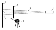
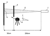
(1)光源からの光を測定フィルム(光学フィルム又は光学積層体)に照射し、測定フィルムを透過した光を投影面に投影する投影法により投影画像を得る工程、
(2)工程(1)の投影法において測定フィルムを用いずに、光源からの光を投影面に投影して、背景画像を得る工程、
及び、
(3)工程(1)で得た投影画像及び工程(2)で得た背景画像をそれぞれグレースケール化により数値化し、数値化された画像データをフーリエ変換して逆空間像(フィルム逆空間像及び背景逆空間像)を得る工程、により得ることができる。上記逆空間像を用いて測定フィルムの面品質を評価することにより、ムラの濃淡と周期を解析することができる。
An optical film included in the optical laminate of the present invention, or a film inverse aerial image obtained by performing a Fourier transform on a projection image obtained by a projection method using the optical laminate of the present invention as a measurement film, and the projection The background inverse aerial image obtained by performing a Fourier transform on the background image obtained without using the measurement film in the method is not particularly limited as long as it is obtained by Fourier transform from the projected image and the background image, respectively. ,
(1) a step of irradiating a measurement film (optical film or optical laminate) with light from a light source and obtaining a projection image by a projection method of projecting light transmitted through the measurement film onto a projection surface;
(2) a step of projecting light from a light source onto a projection surface without using a measurement film in the projection method of step (1) to obtain a background image;
as well as,
(3) The projected image obtained in the step (1) and the background image obtained in the step (2) are each converted into a numerical value by gray scale conversion, and the numerically converted image data is subjected to Fourier transform to obtain an inverse aerial image (film inverse aerial image) And background inverse aerial image). By evaluating the surface quality of the measurement film using the inverse aerial image, the density and period of unevenness can be analyzed.
測定フィルムの投影法による投影画像からフーリエ変換により逆空間像を得る方法は、特に限定されないが、例えば、評価工程について後述する方法を用いてよい。 A method for obtaining an inverse aerial image by Fourier transform from a projection image of the measurement film by a projection method is not particularly limited, but, for example, a method described later for an evaluation step may be used.
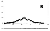
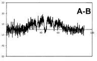
次に、(4)投影画像の逆空間像において直交する2方向の各ラインプロファイルから、背景画像の逆空間像において直交する前記2方向の各ラインプロファイルをそれぞれ引いて、ブランク補正されたラインプロファイルを得る工程、及び、(5)工程(4)で得たブランク補正されたラインプロファイルの最大強度Ymax(それぞれ、Ymh及びYmv)、ならびに各ラインプロファイルにおいて最大強度Ymax(Ymh及びYmv)を示す周波数Xmax(Xmh及びXmv)を測定する。例えば、逆空間像の中心を通る水平方向(h1方向)及び垂直方向(v1方向)のそれぞれの方向についてラインプロファイルを作成する場合について以下に説明する。ラインプロファイルは、例えば図3に示されるような、X軸に周波数、Y軸に強度を表すグラフとして示される。そして、水平方向(h1方向)のラインプロファイルにおける最大強度YmaxをYmh1とし、最大強度Ymh1を示す周波数からブランク補正されたラインプロファイルにおける全周波数の中央値Xcenを引いた値XmaxをXmh1とする。また、垂直方向(v1方向)のラインプロファイルにおける最大強度YmaxをYmv1とし、最大強度Ymv1を示す周波数からブランク補正されたラインプロファイルにおける全周波数の中央値Xcenを引いた値XmaxをXmv1とする。なお、上記例においては、空間像の中心を通る水平方向(h1方向)及び垂直方向(v1方向)を直交する2方向として選択したが、該2方向(h方向及びv方向)は互いに直交していれば特に限定されず、中心を通らない二方向であってもよいし、水平方向及び垂直方向でなくてもよい。なお、本明細書において、「ブランク補正されたラインプロファイル」とは、投影画像の逆空間像において直交する2方向の各ラインプロファイルから、背景画像の逆空間像において直交する前記2方向の各ラインプロファイルをそれぞれ引いて得たラインプロファイルを意味する。上記の操作により、投影画像の逆空間像におけるラインプロファイルのベースラインを補正することができる。 Next, (4) the line profiles in the two directions orthogonal to each other in the inverse aerial image of the background image are subtracted from the line profiles in the two directions orthogonal to each other in the inverse aerial image of the projection image, and the blank-corrected line profiles are obtained. And (5) the maximum intensity Y max (Y mh and Y mv , respectively) of the blank-corrected line profile obtained in step (4), and the maximum intensity Y max (Y mh and Y mh in each line profile). A frequency X max (X mh and X mv ) indicative of Y mv ) is measured. For example, a case will be described below in which line profiles are created in each of the horizontal direction (h1 direction) and the vertical direction (v1 direction) passing through the center of the inverse aerial image. The line profile is shown as a graph showing frequency on the X axis and intensity on the Y axis, for example, as shown in FIG. The maximum intensity Y max in the horizontal (h1 direction) line profile is defined as Y mh1, and a value X max obtained by subtracting the median value X cen of all frequencies in the blank-corrected line profile from the frequency indicating the maximum intensity Y mh1 is obtained. X mh1 . The maximum intensity Y max in the line profile in the vertical direction (v1 direction) is defined as Y mv1, and a value X max obtained by subtracting the median value X cen of all frequencies in the blank-corrected line profile from the frequency indicating the maximum intensity Y mv1 is obtained. X mv1 . In the above example, the horizontal direction (h1 direction) and the vertical direction (v1 direction) passing through the center of the aerial image are selected as two orthogonal directions, but the two directions (h direction and v direction) are orthogonal to each other. The direction is not particularly limited as long as the direction does not pass. The direction may be two directions that do not pass through the center, and may not be the horizontal direction and the vertical direction. In this specification, the “blank-corrected line profile” refers to each line in the two directions orthogonal to each other in the inverse aerial image of the background image from the line profiles in two directions orthogonal to the inverse aerial image of the projection image. It means a line profile obtained by drawing each profile. By the above operation, the baseline of the line profile in the inverse aerial image of the projection image can be corrected.
本発明の光学積層体に含まれる光学フィルムを測定フィルムとして用いて得られる上記Ymh及びYmvは、いずれも40以下である。Ymh又はYmvが40を超える場合、光学フィルムの光学的均質性が十分であるとはいえず、光学積層体の光学的均質性が十分でない場合がある。特に、このような光学フィルムを含む光学積層体の光学的均質性が画像表示装置において使用するに十分であるとはいえず、画像の歪み等を十分に低減することができない。光学積層体の光学的均質性を高めやすく、画像表示装置において画像の視認性を向上しやすい観点から、Ymh及びYmvは、好ましくは35以下、より好ましくは32以下、さらに好ましくは30以下、さらに好ましくは28以下、特に好ましくは26以下である。Ymh及びYmvは小さければ小さいほどよく、その下限は特に限定されず0以上であればよく、通常は1以上である。本発明の光学積層体を測定フィルムとして用いて得られる上記Ymh及びYmvについても、上記好ましい記載が同様にあてはまる。 The above Y mh and Y mv obtained using the optical film contained in the optical laminate of the present invention as a measurement film are both 40 or less. When Y mh or Y mv exceeds 40, the optical homogeneity of the optical film may not be sufficient, and the optical homogeneity of the optical laminate may not be sufficient. In particular, the optical homogeneity of the optical laminate including such an optical film cannot be said to be sufficient for use in an image display device, and image distortion and the like cannot be sufficiently reduced. Y mh and Y mv are preferably 35 or less, more preferably 32 or less, and still more preferably 30 or less, from the viewpoint of easily increasing the optical homogeneity of the optical laminate and easily improving the visibility of an image in an image display device. , More preferably 28 or less, particularly preferably 26 or less. The smaller the values of Y mh and Y mv are, the better. The lower limit is not particularly limited and may be 0 or more, and is usually 1 or more. For even the Y mh and Y mv obtained using the optical laminate of the present invention as a measurement film, the preferred described it applies equally.
本発明の光学積層体に含まれる光学フィルムを測定フィルムとして用いて、上記のようにして得たYmh、Ymv、Xmh及びXmvは、次の関係:
![]()
![]()
測定フィルムとして、本発明の光学積層体に含まれる光学フィルム又は本発明の光学積層体を用いて、上記のようにして得たブランク補正されたラインプロファイルにおける全周波数の中央値をXcenとする。例えば図3に示されるラインプロファイルにおいては、全周波数が90cm−1であり、その中央値である45cm−1がXcenとなる。ここで、Xcenと上記のようにして得たXmh及びXmvとが、次の関係:
![]()
![]()
本発明の光学積層体の少なくとも一方の面の鉛筆硬度は、好ましくはH以上、より好ましくは2H以上、さらに好ましくは3H以上、特に好ましくは4H以上である。光学積層体の少なくとも一方の面の鉛筆硬度が上記の硬度以上である場合、光学積層体の表面における傷等を防止しやすい。上記の鉛筆硬度は、本発明の光学積層体の機能層(好ましくはハードコート層)を有する面の鉛筆硬度であることが好ましい。なお、鉛筆硬度は、JIS K 5600−5−4:1999に準拠して測定でき、例えば実施例に記載の方法により測定できる。 The pencil hardness of at least one surface of the optical laminate of the present invention is preferably H or higher, more preferably 2H or higher, still more preferably 3H or higher, and particularly preferably 4H or higher. When the pencil hardness of at least one surface of the optical laminate is equal to or higher than the above hardness, it is easy to prevent scratches on the surface of the optical laminate. The above pencil hardness is preferably the pencil hardness of the surface of the optical laminate of the present invention having the functional layer (preferably the hard coat layer). The pencil hardness can be measured according to JIS K 5600-5-4: 1999, for example, by the method described in Examples.
本発明の光学積層体の少なくとも一方の面の表面抵抗率は、好ましくは1.0×10¹³Ω/sq以下、より好ましくは5.0×1012Ω/sq以下、さらに好ましくは1.0×1012Ω/sq以下である。表面抵抗率が上記の上限以下である場合、十分な帯電防止機能を得やすい。本発明の光学積層体の少なくとも一方の面の表面抵抗率は、本発明の光学積層体をタッチパネルと組合せて使用する際に、タッチパネルの操作性を担保しやすい観点からは、好ましくは1.0×107Ω/sq以上、より好ましくは5.0×107Ω/sq以上、さらに好ましくは1.0×108Ω/sq以上である。上記の表面抵抗率は、本発明の光学積層体の機能層(好ましくは帯電防止機能層)を有する面の表面抵抗率であることが好ましい。なお、表面抵抗率は、JIS K 6911に準拠して測定でき、例えば実施例に記載の方法により測定できる。 The surface resistivity of at least one surface of the optical laminate of the present invention is preferably 1.0 × 10 13 Ω / sq or less, more preferably 5.0 × 10 12 Ω / sq or less, and still more preferably 1.0 × 10 13 Ω / sq or less. × 10 12 Ω / sq or less. When the surface resistivity is equal to or less than the above upper limit, it is easy to obtain a sufficient antistatic function. The surface resistivity of at least one surface of the optical laminate of the present invention is preferably 1.0 when using the optical laminate of the present invention in combination with a touch panel, from the viewpoint of easily ensuring the operability of the touch panel. × 10 7 Ω / sq or more, more preferably 5.0 × 10 7 Ω / sq or more, still more preferably 1.0 × 10 8 Ω / sq or more. The above surface resistivity is preferably the surface resistivity of the surface of the optical laminate of the present invention having the functional layer (preferably the antistatic functional layer). The surface resistivity can be measured according to JIS K 6911, for example, by the method described in Examples.
本発明の光学積層体において、機能層を有する面から光を入射した場合の光学積層体の反射率は、好ましくは3.0%以下、より好ましくは2.0%以下、さらに好ましくは1.0%以下である。なお、本明細書における反射率は、視感度補正反射率を意味し、具体的には、入射角12度で光を入射したときの反射角12度における波長350〜900nmの範囲の分光反射率(すなわち入射角12度における正反射率)をJIS Z 8701の2度視野(C光源)により視感度補正した反射率をいう。反射率は、分光光度計等を用いて測定することができる。反射率の測定において、光を入射させる機能層面とは反対側の面からの反射が測定値に影響を及ぼす可能性を排除する目的、及び、光学積層体の反りを防止する目的のために、光学積層体の、光を入射させる機能層面とは反対側の面を、光学的に透明な粘着剤を用いて黒色板(黒色アクリル板等)に貼合した試料を、測定用試料として用いる。 In the optical laminate of the present invention, the reflectance of the optical laminate when light is incident from the surface having the functional layer is preferably 3.0% or less, more preferably 2.0% or less, and further preferably 1. 0% or less. In addition, the reflectance in this specification means a visibility correction reflectance, and specifically, a spectral reflectance in a wavelength range of 350 to 900 nm at a reflection angle of 12 degrees when light is incident at an incident angle of 12 degrees. (Specific reflectance at an incident angle of 12 degrees) is a reflectance obtained by correcting luminosity by a 2-degree visual field (C light source) according to JIS Z8701. The reflectance can be measured using a spectrophotometer or the like. In the measurement of the reflectance, for the purpose of eliminating the possibility that the reflection from the surface opposite to the functional layer surface on which light is incident affects the measured value, and for the purpose of preventing warpage of the optical laminate, A sample in which the surface of the optical laminate opposite to the functional layer surface on which light is incident is bonded to a black plate (eg, a black acrylic plate) using an optically transparent adhesive is used as a measurement sample.
本発明の光学積層体の黄色度(YI値)は、好ましくは3.0以下、より好ましくは2.7以下、さらに好ましくは2.5以下、特に好ましくは2.0以下である。光学積層体の黄色度が上記の上限以下であると透明性を向上させやすく、例えば表示装置の前面板に使用した場合に視認性を高めやすい。黄色度は、通常−5以上、好ましくは−2以上、より好ましくは0以上、さらに好ましくは0.3以上、さらに好ましくは0.5以上、特に好ましくは0.7以上である。黄色度(YI)は、JIS K 7373:2006に準拠して、紫外可視近赤外分光光度計を用いて300〜800nmの光に対する透過率測定を行い、3刺激値(X、Y、Z)を求め、YI=100×(1.2769X−1.0592Z)/Yの式に基づいて算出できる。 The yellowness (YI value) of the optical laminate of the present invention is preferably 3.0 or less, more preferably 2.7 or less, further preferably 2.5 or less, and particularly preferably 2.0 or less. When the yellowness of the optical laminate is equal to or less than the above upper limit, the transparency is easily improved. For example, when the optical laminate is used for a front panel of a display device, the visibility is easily improved. Yellowness is usually -5 or more, preferably -2 or more, more preferably 0 or more, further preferably 0.3 or more, further preferably 0.5 or more, and particularly preferably 0.7 or more. The yellowness (YI) is measured based on JIS K 7373: 2006 by using an ultraviolet-visible-near-infrared spectrophotometer to measure the transmittance of light having a wavelength of 300 to 800 nm, and tristimulus values (X, Y, Z) And YI = 100 × (1.2769X−1.0592Z) / Y.
本発明の光学積層体の全光線透過率は、好ましくは80%以上、より好ましくは85%以上、さらに好ましくは90%以上である。全光線透過率が上記の下限以上であると、光学積層体を画像表示装置に組み込んだ際に視認性を高めやすい。本発明の光学積層体は、光学的均質性が高く、高い透過率を示すので、例えば、透過率の低いフィルムを用いた場合と比べて、一定の明るさを得るため必要な表示素子等の発光強度を抑えることが可能となる。このため、消費電力を削減することができる。例えば、本発明の光学積層体を表示装置に組みこむ場合、バックライトの光量を減らしても明るい表示を得られる傾向があり、エネルギーの節約に貢献できる。全光線透過率の上限は、通常100%以下である。なお、全光線透過率は、例えばJIS K 7361−1:1997に準拠してヘイズコンピュータを用いて測定できる。全光線透過率は、後述する光学積層体の厚さの範囲における全光線透過率であってよい。 The total light transmittance of the optical laminate of the present invention is preferably 80% or more, more preferably 85% or more, and further preferably 90% or more. When the total light transmittance is equal to or more than the above lower limit, visibility is easily increased when the optical laminate is incorporated in an image display device. The optical laminate of the present invention has a high optical homogeneity and a high transmittance, so that, for example, as compared with a case where a film having a low transmittance is used, a display element or the like necessary to obtain a constant brightness is required. Light emission intensity can be suppressed. Therefore, power consumption can be reduced. For example, when the optical laminate of the present invention is incorporated in a display device, there is a tendency that a bright display is obtained even if the light amount of the backlight is reduced, which can contribute to energy saving. The upper limit of the total light transmittance is usually 100% or less. The total light transmittance can be measured using a haze computer in accordance with, for example, JIS K7361-1: 1997. The total light transmittance may be the total light transmittance in the range of the thickness of the optical laminate described later.
本発明の光学積層体のヘイズは、好ましくは3.0%以下、より好ましくは2.0%以下、さらに好ましくは1.0%以下、さらにより好ましくは0.5%以下、特に好ましくは0.3%以下である。光学積層体のヘイズが上記の上限以下であると透明性が良好となり、例えば画像表示装置の前面板に使用した場合に、画像の視認性を高めやすい。またヘイズの下限は通常0.01%以上である。なお、ヘイズは、JIS K 7136:2000に準拠してヘイズコンピュータを用いて測定できる。 The haze of the optical laminate of the present invention is preferably 3.0% or less, more preferably 2.0% or less, further preferably 1.0% or less, still more preferably 0.5% or less, and particularly preferably 0% or less. 0.3% or less. When the haze of the optical laminate is equal to or less than the above upper limit, transparency becomes good, and when used for a front plate of an image display device, for example, the visibility of an image is easily increased. The lower limit of the haze is usually at least 0.01%. The haze can be measured using a haze computer in accordance with JIS K 7136: 2000.
本発明の光学積層体の厚さは、用途に応じて適宜調整してよいが、好ましくは25μm以上、より好ましくは27μm以上、さらに好ましくは30μm以上であり、好ましくは100μm以下、より好ましくは90μm以下、さらに好ましくは85μm以下である。光学積層体の厚さは、膜厚計などで測定でき、例えば実施例に記載の方法により測定できる。 The thickness of the optical laminate of the present invention may be appropriately adjusted depending on the application, but is preferably 25 μm or more, more preferably 27 μm or more, still more preferably 30 μm or more, preferably 100 μm or less, more preferably 90 μm or less. The thickness is more preferably 85 μm or less. The thickness of the optical laminate can be measured with a film thickness meter or the like, and can be measured, for example, by the method described in Examples.
本発明の光学積層体は、ポリイミド系樹脂及び/又はポリアミド系樹脂を含む光学フィルムと、該光学フィルムの少なくとも片面に積層された機能層とを有する。Ymh等に関する上記特徴を有する均質性の高い光学フィルムを製造しやすい観点、及び/又は、上記特徴を有する均質性の高い光学積層体を製造しやすい観点からは、本発明の光学積層体における光学フィルムは、好ましくはキャストフィルムである。本明細書において、キャストフィルムとは、例えば、上記樹脂を含む溶液、分散液、又は溶融物を、適当な支持体上に流延、塗布等し、加熱、冷却、乾燥等により塗膜化させて、必要に応じて該塗膜を該支持体から剥離して得られるフィルムを表す。このようにして得たフィルムは、ポリイミド系樹脂及び/又はポリアミド系樹脂を少なくとも含有し、場合により微量の溶媒を含有する。 The optical laminate of the present invention has an optical film containing a polyimide resin and / or a polyamide resin, and a functional layer laminated on at least one surface of the optical film. From the viewpoint of easily producing an optical film having high homogeneity having the above-mentioned characteristics relating to Y MH and / or the like, and / or from the viewpoint of easily producing an optical laminate having high homogeneity having the above-mentioned characteristics, the optical laminate of the present invention is preferably used. The optical film is preferably a cast film. In the present specification, the cast film is, for example, a solution, a dispersion, or a melt containing the resin, cast on a suitable support, coated or the like, and heated, cooled, dried, or the like to form a film. Represents a film obtained by peeling the coating film from the support as necessary. The film thus obtained contains at least a polyimide resin and / or a polyamide resin, and optionally contains a trace amount of a solvent.
本発明の光学積層体における光学フィルムは、ポリイミド系樹脂及び/又はポリアミド系樹脂を含む。本発明の光学積層体において、光学フィルムは、1種類のポリイミド系樹脂又はポリアミド系樹脂を含有してもよいし、2種以上のポリイミド系樹脂及び/又はポリアミド系樹脂を含有してもよい。 The optical film in the optical laminate of the present invention contains a polyimide resin and / or a polyamide resin. In the optical laminate of the present invention, the optical film may contain one kind of polyimide resin or polyamide resin, or may contain two or more kinds of polyimide resin and / or polyamide resin.
<ポリイミド系樹脂及びポリアミド系樹脂>
本発明の光学積層体において、光学フィルムは、ポリイミド系樹脂及び/又はポリアミド系樹脂を含む。ポリイミド系樹脂とは、イミド基を含む繰返し構造単位を含有する樹脂(以下、ポリイミド樹脂ということがある)、並びにイミド基及びアミド基の両方を含む繰返し構造単位を含有する樹脂(以下、ポリアミドイミド樹脂ということがある)からなる群から選択される少なくとも1種の樹脂を示す。また、ポリアミド系樹脂とは、アミド基を含む繰り返し構造単位を含有する樹脂を示す。
<Polyimide resin and polyamide resin>
In the optical laminate of the present invention, the optical film contains a polyimide resin and / or a polyamide resin. The polyimide resin is a resin containing a repeating structural unit containing an imide group (hereinafter, sometimes referred to as a polyimide resin) and a resin containing a repeating structural unit containing both an imide group and an amide group (hereinafter, a polyamideimide). At least one resin selected from the group consisting of: Further, the polyamide-based resin refers to a resin containing a repeating structural unit containing an amide group.
本発明の好ましい一実施形態において、ポリイミド系樹脂は、式(1)で表される構成単位を有するポリイミド樹脂であるか、又は、式(1)で表される構成単位及び式(2)で表される構成単位を有するポリアミドイミド樹脂であることが好ましい。また、ポリアミド系樹脂は、式(2)で表される構成単位を有するポリアミド樹脂であることが好ましい。以下において式(1)及び式(2)について説明するが、式(1)についての説明は、ポリイミド樹脂及びポリアミドイミド樹脂の両方に関し、式(2)についての説明は、ポリアミド樹脂及びポリアミドイミド樹脂の両方に関する。
式(1)で表される構成単位は、テトラカルボン酸化合物とジアミン化合物とが反応して形成される構成単位であり、式(2)で表される構成単位は、ジカルボン酸化合物とジアミン化合物とが反応して形成される構成単位である。 The structural unit represented by the formula (1) is a structural unit formed by reacting a tetracarboxylic acid compound and a diamine compound, and the structural unit represented by the formula (2) is a dicarboxylic acid compound and a diamine compound Is a structural unit formed by the reaction.
式(2)において、Zは、2価の有機基であり、好ましくは炭素数1〜8の炭化水素基又はフッ素置換された炭素数1〜8の炭化水素基で置換されていてもよい、炭素数4〜40の2価の有機基であり、より好ましくは炭素数1〜8の炭化水素基又はフッ素置換された炭素数1〜8の炭化水素基で置換されていてもよい、環状構造を有する炭素数4〜40の2価の有機基である。環状構造としては、脂環、芳香環、ヘテロ環構造が挙げられる。Zの有機基として、後述する式(20)、式(21)、式(22)、式(23)、式(24)、式(25)、式(26)、式(27)、式(28)及び式(29)で表される基の結合手のうち、隣接しない2つが水素原子に置き換わった基及び炭素数6以下の2価の鎖式炭化水素基が例示され、Zのヘテロ環構造としてはチオフェン環骨格を有する基が例示される。光学フィルムの黄色度を抑制(YI値を低減)しやすい観点から、式(20)〜式(27)で表される基、及び、チオフェン環骨格を有する基が好ましい。 In the formula (2), Z is a divalent organic group, and may be preferably substituted with a hydrocarbon group having 1 to 8 carbon atoms or a fluorine-substituted hydrocarbon group having 1 to 8 carbon atoms. A cyclic structure which is a divalent organic group having 4 to 40 carbon atoms, and may be more preferably substituted with a hydrocarbon group having 1 to 8 carbon atoms or a fluorine-substituted hydrocarbon group having 1 to 8 carbon atoms. And a divalent organic group having 4 to 40 carbon atoms. Examples of the cyclic structure include an alicyclic, aromatic, and heterocyclic structure. As the organic group of Z, the following formulas (20), (21), (22), (23), (24), (25), (26), (27), and ( 28) and the bond of the group represented by the formula (29), a group in which two non-adjacent atoms are replaced by a hydrogen atom and a divalent chain hydrocarbon group having 6 or less carbon atoms are exemplified. Examples of the structure include a group having a thiophene ring skeleton. From the viewpoint of easily suppressing the yellowness of the optical film (reducing the YI value), groups represented by the formulas (20) to (27) and a group having a thiophene ring skeleton are preferable.
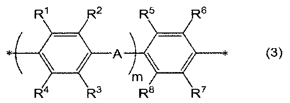
本発明の一実施形態において、ポリアミド樹脂及びポリアミドイミド樹脂は、複数種のZを含み得、複数種のZは、互いに同一であっても異なっていてもよい。特に、光学フィルムの表面硬度を高めやすい観点及び光学特性を向上させやすい観点から、Zの少なくとも一部が、式(3)
Aは、互いに独立に、単結合、−O−、−CH2−、−CH2−CH2−、−CH(CH3)−、−C(CH3)2−、−C(CF3)2−、−SO2−、−S−、−CO−又は−N(R9)−を表し、R9は水素原子、ハロゲン原子で置換されていてもよい炭素数1〜12の1価の炭化水素基を表し、
mは0〜4の整数であり、
*は結合手を表す]
で表されることが好ましい。
In one embodiment of the present invention, the polyamide resin and the polyamide-imide resin may include a plurality of types of Z, and the plurality of types of Z may be the same or different from each other. Particularly, from the viewpoint of easily increasing the surface hardness of the optical film and improving the optical characteristics, at least a part of Z is represented by the formula (3).
A is, independently of one another, a single bond, -O -, - CH 2 - , - CH 2 -CH 2 -, - CH (CH 3) -, - C (CH 3) 2 -, - C (CF 3) 2 -, - SO 2 -, - S -, - CO- or -N (R 9) - represents, R 9 is a hydrogen atom, monovalent 1-12 carbon atoms which may be substituted with a halogen atom Represents a hydrocarbon group,
m is an integer of 0 to 4,
* Represents a bond]
Is preferably represented by
式(3)において、Aは、単結合、−O−、−CH2−、−CH2−CH2−、−CH(CH3)−、−C(CH3)2−、−C(CF3)2−、−SO2−、−S−、−CO−又は−N(R9)−を表し、光学フィルムの耐屈曲性の観点から、好ましくは−O−又は−S−を表し、より好ましくは−O−を表す。
R1、R2、R3、R4、R5、R6、R7、R8は、互いに独立に、水素原子、炭素数1〜6のアルキル基、炭素数1〜6のアルコキシ基、又は炭素数6〜12のアリール基を表す。炭素数1〜6のアルキル基としては、例えばメチル基、エチル基、n−プロピル基、イソプロピル基、n−ブチル基、sec−ブチル基、tert−ブチル基、n−ペンチル基、2−メチル−ブチル基、3−メチルブチル基、2−エチル−プロピル基、n−ヘキシル基等が挙げられる。炭素数1〜6のアルコキシ基としては、例えばメトキシ基、エトキシ基、プロピルオキシ基、イソプロピルオキシ基、ブトキシ基、イソブトキシ基、tert−ブトキシ基、ペンチルオキシ基、ヘキシルオキシ基、シクロヘキシルオキシ基等が挙げられる。炭素数6〜12のアリール基としては、例えばフェニル基、トリル基、キシリル基、ナフチル基、ビフェニル基等が挙げられる。光学フィルムの表面硬度及び柔軟性の観点から、R1〜R8は、互いに独立に、好ましくは水素原子又は炭素数1〜6のアルキル基を表し、より好ましくは水素原子又は炭素数1〜3のアルキル基を表し、さらに好ましくは水素原子を表す。ここで、R1〜R8に含まれる水素原子は、互いに独立に、ハロゲン原子で置換されていてもよい。
R9は水素原子、ハロゲン原子で置換されていてもよい炭素数1〜12の1価の炭化水素基を表す。炭素数1〜12の1価の炭化水素基としては、例えばメチル基、エチル基、n−プロピル基、イソプロピル基、n−ブチル基、sec−ブチル基、tert−ブチル基、n−ペンチル基、2−メチル−ブチル基、3−メチルブチル基、2−エチル−プロピル基、n−ヘキシル、n−ヘプチル基、n−オクチル基、tert−オクチル基、n−ノニル基、n−デシル基等が挙げられ、これらはハロゲン原子で置換されていてもよい。前記ハロゲン原子としては、フッ素原子、塩素原子、臭素原子、ヨウ素原子などが挙げられる。ポリイミド系樹脂又はポリアミド系樹脂は、複数種のAを含み得、複数種のAは、互いに同一でよく、異なっていてもよい。
In the formula (3), A is a single bond, -O -, - CH 2 - , - CH 2 -CH 2 -, - CH (CH 3) -, - C (CH 3) 2 -, - C (CF 3) 2 -, - SO 2 -, - S -, - CO- or -N (R 9) - represents, in terms of flex resistance of the optical film, preferably represents -O- or -S-, More preferably, it represents -O-.
R 1 , R 2 , R 3 , R 4 , R 5 , R 6 , R 7 , and R 8 are each independently a hydrogen atom, an alkyl group having 1 to 6 carbon atoms, an alkoxy group having 1 to 6 carbon atoms, Alternatively, it represents an aryl group having 6 to 12 carbon atoms. Examples of the alkyl group having 1 to 6 carbon atoms include methyl, ethyl, n-propyl, isopropyl, n-butyl, sec-butyl, tert-butyl, n-pentyl, and 2-methyl-. Butyl, 3-methylbutyl, 2-ethyl-propyl, n-hexyl and the like. Examples of the alkoxy group having 1 to 6 carbon atoms include a methoxy group, an ethoxy group, a propyloxy group, an isopropyloxy group, a butoxy group, an isobutoxy group, a tert-butoxy group, a pentyloxy group, a hexyloxy group and a cyclohexyloxy group. No. Examples of the aryl group having 6 to 12 carbon atoms include a phenyl group, a tolyl group, a xylyl group, a naphthyl group, and a biphenyl group. From the viewpoint of the surface hardness and flexibility of the optical film, R 1 to R 8 independently represent a hydrogen atom or an alkyl group having 1 to 6 carbon atoms, and more preferably a hydrogen atom or 1 to 3 carbon atoms. And more preferably a hydrogen atom. Here, the hydrogen atoms contained in R 1 to R 8 may be independently substituted with halogen atoms.
R 9 represents a monovalent hydrocarbon group having 1 to 12 carbon atoms which may be substituted with a hydrogen atom or a halogen atom. Examples of the monovalent hydrocarbon group having 1 to 12 carbon atoms include a methyl group, an ethyl group, an n-propyl group, an isopropyl group, an n-butyl group, a sec-butyl group, a tert-butyl group, an n-pentyl group, 2-methyl-butyl group, 3-methylbutyl group, 2-ethyl-propyl group, n-hexyl, n-heptyl group, n-octyl group, tert-octyl group, n-nonyl group, n-decyl group and the like. And these may be substituted with a halogen atom. Examples of the halogen atom include a fluorine atom, a chlorine atom, a bromine atom, and an iodine atom. The polyimide-based resin or the polyamide-based resin may include a plurality of types of A, and the plurality of types A may be the same as or different from each other.
式(3)において、mは、0〜4の範囲の整数であり、mがこの範囲内であると、光学フィルムの耐屈曲性や弾性率が良好になりやすい。また、式(3)において、mは、好ましくは0〜3の範囲の整数、より好ましくは0〜2、さらに好ましくは0又は1、特に好ましくは0である。mがこの範囲内であると、光学フィルムの耐屈曲性や弾性率を向上させやすい。また、Zは、式(3)で表される構成単位を1種又は2種類以上含んでいてもよく、光学フィルムの弾性率及び耐屈曲性の向上、黄色度(YI値)低減の観点から、特にmの値が異なる2種類以上の構成単位、好ましくはmの値の異なる2種類の構成単位を含んでいてもよい。その場合、光学フィルムの高い弾性率、耐屈曲性及び低い黄色度(YI値)を発現しやすい観点から、樹脂がZにおいて、mが0である式(3)で表される構成単位を含有することが好ましく、該構成単位に加えてmが1である式(3)で表される構成単位をさらに含有することがより好ましい。 In the formula (3), m is an integer in the range of 0 to 4, and when m is within this range, the bending resistance and the elastic modulus of the optical film tend to be good. In the formula (3), m is preferably an integer in the range of 0 to 3, more preferably 0 to 2, further preferably 0 or 1, and particularly preferably 0. When m is within this range, the bending resistance and the elastic modulus of the optical film can be easily improved. In addition, Z may include one or more types of the structural unit represented by the formula (3), and from the viewpoint of improving the elastic modulus and bending resistance of the optical film and reducing the yellowness (YI value). In particular, it may include two or more types of structural units having different values of m, preferably two types of structural units having different values of m. In that case, from the viewpoint of easily exhibiting a high elastic modulus, bending resistance and low yellowness (YI value) of the optical film, the resin contains a structural unit represented by Formula (3) where m is 0 in Z. It is more preferable to further include a structural unit represented by the formula (3) in which m is 1 in addition to the structural unit.
本発明の好ましい一実施形態において、樹脂は、式(3)で表される構成単位として、m=0であり、かつR5〜R8が水素原子である構成単位を有する。より好ましい本発明の一実施形態において、樹脂は、式(3)で表される構成単位として、m=0であり、かつR5〜R8が水素原子である構成単位と、式(3’):
光学積層体が、ポリアミドイミド樹脂を含む光学フィルムを有する、本発明の好ましい一実施形態において、ポリアミドイミド樹脂の式(1)で表される構成単位及び式(2)で表される構成単位の合計を100モル%としたときに、式(3)で表される構成単位の割合は、好ましくは20モル%以上、より好ましくは30モル%以上、さらに好ましくは40モル%以上、特に好ましくは50モル%以上、最も好ましくは60モル%以上であり、好ましくは90モル%以下、より好ましくは85モル%以下、さらに好ましくは80モル%以下である。式(3)で表される構成単位の割合が上記の下限以上であると、光学フィルムの表面硬度を高めやすく、かつ耐屈曲性や弾性率を高めやすい。式(3)で表される構成単位の割合が上記の上限以下であると、式(3)由来のアミド結合間水素結合による樹脂含有ワニスの粘度上昇を抑制し、フィルムの加工性を向上しやすい。 In a preferred embodiment of the present invention in which the optical laminate has an optical film containing a polyamide-imide resin, the polyamide-imide resin has a structural unit represented by the formula (1) and a structural unit represented by the formula (2). When the total is 100 mol%, the proportion of the structural unit represented by the formula (3) is preferably at least 20 mol%, more preferably at least 30 mol%, further preferably at least 40 mol%, particularly preferably. It is at least 50 mol%, most preferably at least 60 mol%, preferably at most 90 mol%, more preferably at most 85 mol%, further preferably at most 80 mol%. When the proportion of the structural unit represented by the formula (3) is equal to or more than the above lower limit, the surface hardness of the optical film is easily increased, and the bending resistance and the elastic modulus are easily increased. When the proportion of the structural unit represented by the formula (3) is equal to or less than the above upper limit, the increase in the viscosity of the resin-containing varnish due to the hydrogen bond between the amide bonds derived from the formula (3) is suppressed, and the processability of the film is improved. Cheap.
また、ポリアミドイミド樹脂がm=1〜4である式(3)の構成単位を有する場合、ポリアミドイミド樹脂の式(1)で表される構成単位及び式(2)で表される構成単位の合計を100モル%としたときに、mが1〜4である式(3)の構成単位の割合は、好ましくは3モル%以上、より好ましくは5モル%以上、さらに好ましくは7モル%以上、特に好ましくは9モル%以上であり、好ましくは90モル%以下、より好ましくは70モル%以下、さらに好ましくは50モル%以下、特に好ましくは30モル%以下である。mが1〜4である式(3)の構成単位の割合が上記の下限以上であると、光学フィルムの表面硬度及び耐屈曲性を高めやすい。mが1〜4である式(3)の構成単位の割合が上記の上限以下であると、式(3)由来のアミド結合間水素結合による樹脂含有ワニスの粘度上昇を抑制し、フィルムの加工性を向上しやすい。なお、式(1)、式(2)又は式(3)で表される構成単位の含有量は、例えば1H−NMRを用いて測定することができ、又は原料の仕込み比から算出することもできる。 When the polyamide-imide resin has a structural unit represented by the formula (3) in which m = 1 to 4, the structural unit represented by the formula (1) and the structural unit represented by the formula (2) of the polyamide-imide resin are When the total is 100 mol%, the proportion of the structural unit of the formula (3) in which m is 1 to 4 is preferably 3 mol% or more, more preferably 5 mol% or more, and further preferably 7 mol% or more. It is particularly preferably at least 9 mol%, preferably at most 90 mol%, more preferably at most 70 mol%, further preferably at most 50 mol%, particularly preferably at most 30 mol%. When the ratio of the structural unit of the formula (3) in which m is 1 to 4 is equal to or more than the above lower limit, the surface hardness and the bending resistance of the optical film are easily increased. When the ratio of the structural unit of the formula (3) in which m is 1 to 4 is equal to or less than the above upper limit, the increase in the viscosity of the resin-containing varnish due to the hydrogen bond between the amide bonds derived from the formula (3) is suppressed, and the film is processed. Easy to improve the performance. In addition, the content of the structural unit represented by the formula (1), the formula (2) or the formula (3) can be measured, for example, using 1 H-NMR, or calculated from the charging ratio of the raw materials. Can also.
本発明の好ましい一実施形態において、上記ポリアミド樹脂又はポリアミドイミド樹脂中のZの、好ましくは30モル%以上、より好ましくは40モル%以上、さらに好ましくは45モル%以上、さらに好ましくは50モル%以上、特に好ましくは70モル%以上が、mが0〜4である式(3)で表される構成単位である。Zの上記の下限以上が、mが0〜4である式(3)で表される構成単位であると、光学フィルムの表面硬度を高めやすいと共に、耐屈曲性及び弾性率も高めやすい。また、ポリアミド樹脂又はポリアミドイミド樹脂中のZの100モル%以下が、mが0〜4である式(3)で表される構成単位であればよい。なお、樹脂中の、mが0〜4である式(3)で表される構成単位の割合は、例えば1H−NMRを用いて測定することができ、又は原料の仕込み比から算出することもできる。 In a preferred embodiment of the present invention, the content of Z in the polyamide resin or polyamideimide resin is preferably at least 30 mol%, more preferably at least 40 mol%, further preferably at least 45 mol%, further preferably at least 50 mol%. As described above, particularly preferably 70 mol% or more is a structural unit represented by the formula (3) in which m is 0 to 4. When the above-mentioned lower limit of Z is a structural unit represented by the formula (3) in which m is 0 to 4, the surface hardness of the optical film is easily increased, and the bending resistance and the elastic modulus are also easily increased. Further, 100 mol% or less of Z in the polyamide resin or polyamideimide resin may be a structural unit represented by the formula (3) in which m is 0 to 4. In addition, the ratio of the structural unit represented by the formula (3) in which m is 0 to 4 in the resin can be measured, for example, using 1 H-NMR, or calculated from the charging ratio of the raw materials. You can also.
本発明の好ましい一実施形態において、上記ポリアミド樹脂又はポリアミドイミド樹脂中のZの、好ましくは5モル%以上、より好ましくは8モル%以上、さらに好ましくは10モル%以上、特に好ましくは12モル%以上が、mが1〜4である式(3)で表される。ポリアミドイミド樹脂のZの上記の下限以上が、mが1〜4である式(3)で表されると、光学フィルムの表面硬度を高めやすく、かつ耐屈曲性及び弾性率を高めやすい。また、Zの、好ましくは90モル%以下、より好ましくは70モル%以下、さらに好ましくは50モル%以下、特に好ましくは30モル%以下が、mが1〜4である式(3)で表されることが好ましい。Zの上記の上限以下が、mが1〜4である式(3)で表されると、mが1〜4である式(3)由来のアミド結合間水素結合による樹脂含有ワニスの粘度上昇を抑制し、フィルムの加工性を向上しやすい。なお樹脂中のmが1〜4である式(3)で表される構成単位の割合は、例えば1H−NMRを用いて測定することができ、又は原料の仕込み比から算出することもできる。 In a preferred embodiment of the present invention, the content of Z in the polyamide resin or the polyamideimide resin is preferably at least 5 mol%, more preferably at least 8 mol%, further preferably at least 10 mol%, particularly preferably at least 12 mol%. The above is represented by Expression (3) in which m is 1 to 4. When the above-mentioned lower limit of Z of the polyamide-imide resin is represented by the formula (3) in which m is 1 to 4, the surface hardness of the optical film is easily increased, and the bending resistance and the elastic modulus are easily increased. Further, Z is preferably 90 mol% or less, more preferably 70 mol% or less, still more preferably 50 mol% or less, and particularly preferably 30 mol% or less. Preferably. When the above-mentioned upper limit of Z is represented by the formula (3) in which m is 1 to 4, the viscosity increase of the resin-containing varnish due to the hydrogen bond between the amide bonds derived from the formula (3) in which m is 1 to 4 And it is easy to improve the processability of the film. The proportion of the structural unit represented by the formula (3) in which m is 1 to 4 in the resin can be measured, for example, using 1 H-NMR, or can be calculated from the charging ratio of the raw materials. .
式(1)及び式(2)において、Xは、互いに独立に、2価の有機基を表し、好ましくは炭素数4〜40の2価の有機基、より好ましくは環状構造を有する炭素数4〜40の2価の有機基を表す。環状構造としては、脂環、芳香環、ヘテロ環構造が挙げられる。前記有機基は、有機基中の水素原子が炭化水素基又はフッ素置換された炭化水素基で置換されていてもよく、その場合、炭化水素基及びフッ素置換された炭化水素基の炭素数は好ましくは1〜8である。本発明の一実施形態において、ポリイミド樹脂又はポリアミドイミド樹脂は、複数種のXを含み得、複数種のXは、互いに同一でよく、異なっていてもよい。Xとしては、式(10)、式(11)、式(12)、式(13)、式(14)、式(15)、式(16)、式(17)及び式(18)で表される基;それらの式(10)〜式(18)で表される基中の水素原子がメチル基、フルオロ基、クロロ基又はトリフルオロメチル基で置換された基;並びに炭素数6以下の鎖式炭化水素基が例示される。 In the formulas (1) and (2), X independently represents a divalent organic group, preferably a divalent organic group having 4 to 40 carbon atoms, more preferably 4 carbon atoms having a cyclic structure. Represents a divalent organic group of 4040. Examples of the cyclic structure include an alicyclic, aromatic, and heterocyclic structure. The organic group, a hydrogen atom in the organic group may be substituted with a hydrocarbon group or a fluorine-substituted hydrocarbon group, in which case the carbon number of the hydrocarbon group and the fluorine-substituted hydrocarbon group is preferably Is 1 to 8. In one embodiment of the present invention, the polyimide resin or the polyamide-imide resin may include a plurality of types of X, and the plurality of types of X may be the same as or different from each other. X is represented by Expression (10), Expression (11), Expression (12), Expression (13), Expression (14), Expression (15), Expression (16), Expression (17), and Expression (18). A group in which a hydrogen atom in those groups represented by the formulas (10) to (18) is substituted with a methyl group, a fluoro group, a chloro group or a trifluoromethyl group; and a group having 6 or less carbon atoms A chain hydrocarbon group is exemplified.
式(10)〜式(18)中、*は結合手を表し、
V1、V2及びV3は、互いに独立に、単結合、−O−、−S−、−CH2−、−CH2−CH2−、−CH(CH3)−、−C(CH3)2−、−C(CF3)2−、−SO2−、−CO−又は−N(Q)−を表す。ここで、Qはハロゲン原子で置換されていてもよい炭素数1〜12の1価の炭化水素基を表す。炭素数1〜12の1価の炭化水素基としては、R9について上記に述べた基が挙げられる。
1つの例は、V1及びV3が単結合、−O−又は−S−であり、かつ、V2が−CH2−、−C(CH3)2−、−C(CF3)2−又は−SO2−である。V1とV2との各環に対する結合位置、及び、V2とV3との各環に対する結合位置は、互いに独立に、好ましくは各環に対してメタ位又はパラ位であり、より好ましくはパラ位である。
In the formulas (10) to (18), * represents a bond,
V 1, V 2 and V 3 independently of one another, a single bond, -O -, - S -, - CH 2 -, - CH 2 -CH 2 -, - CH (CH 3) -, - C (CH 3) 2 -, - C ( CF 3) 2 -, - SO 2 -, - CO- or -N (Q) - represents a. Here, Q represents a monovalent hydrocarbon group having 1 to 12 carbon atoms which may be substituted with a halogen atom. Examples of the monovalent hydrocarbon group having 1 to 12 carbon atoms include the groups described above for R 9 .
One example is a single bond V 1 and V 3, -O- or -S-, and, V 2 is -CH 2 -, - C (CH 3) 2 -, - C (CF 3) 2 — Or —SO 2 —. The bonding position of V 1 and V 2 to each ring and the bonding position of V 2 and V 3 to each ring are independently of each other, preferably meta or para to each ring, more preferably Is in para position.
式(10)〜式(18)で表される基の中でも、光学フィルムの表面硬度及び耐屈曲性を高めやすい観点から、式(13)、式(14)、式(15)、式(16)及び式(17)で表される基が好ましく、式(14)、式(15)及び式(16)で表される基がより好ましい。また、V1、V2及びV3は、光学フィルムの表面硬度及び柔軟性を高めやすい観点から、互いに独立に、単結合、−O−又は−S−であることが好ましく、単結合又は−O−であることがより好ましい。 Among the groups represented by the formulas (10) to (18), from the viewpoint of easily increasing the surface hardness and the bending resistance of the optical film, the formulas (13), (14), (15), and (16) are preferable. ) And the group represented by the formula (17) are preferable, and the groups represented by the formulas (14), (15) and (16) are more preferable. In addition, V 1 , V 2 and V 3 are preferably each independently a single bond, —O— or —S— from the viewpoint of easily increasing the surface hardness and flexibility of the optical film, and a single bond or − More preferably, it is O-.
本発明の好ましい一実施形態において、式(1)及び式(2)中の複数のXの少なくとも一部は、式(4):
で表される構成単位である。式(1)及び式(2)中の複数のXの少なくとも一部が式(4)で表される基であると、光学フィルムの表面硬度及び透明性を高めやすい。
In a preferred embodiment of the present invention, at least a part of the plurality of Xs in the formulas (1) and (2) is represented by the formula (4):
Is a structural unit represented by When at least a part of the plurality of Xs in the formulas (1) and (2) is a group represented by the formula (4), the surface hardness and the transparency of the optical film are easily increased.
式(4)において、R10、R11、R12、R13、R14、R15、R16及びR17は、互いに独立に、水素原子、炭素数1〜6のアルキル基、炭素数1〜6のアルコキシ基又は炭素数6〜12のアリール基を表す。炭素数1〜6のアルキル基、炭素数1〜6のアルコキシ基又は炭素数6〜12のアリール基としては、式(3)における炭素数1〜6のアルキル基、炭素数1〜6のアルコキシ基又は炭素数6〜12のアリール基として例示のものが挙げられる。R10〜R17は、互いに独立に、好ましくは水素原子又は炭素数1〜6のアルキル基を表し、より好ましくは水素原子又は炭素数1〜3のアルキル基を表し、ここで、R10〜R17に含まれる水素原子は、互いに独立に、ハロゲン原子で置換されていてもよい。ハロゲン原子としては、例えばフッ素原子、塩素原子、臭素原子、ヨウ素原子が挙げられる。R10〜R17は、互いに独立に、光学フィルムの表面硬度、透明性及び耐屈曲性の観点から、さらに好ましくは水素原子、メチル基、フルオロ基、クロロ基又はトリフルオロメチル基であり、とりわけ好ましくはR10、R12、R13、R14、R15及びR16が水素原子、R11及びR17が水素原子、メチル基、フルオロ基、クロロ基又はトリフルオロメチル基であり、特に好ましくはR11及びR17がメチル基又はトリフルオロメチル基である。 In the formula (4), R 10 , R 11 , R 12 , R 13 , R 14 , R 15 , R 16 and R 17 are each independently a hydrogen atom, an alkyl group having 1 to 6 carbon atoms, and 1 carbon atom. Represents an alkoxy group having 6 to 6 carbon atoms or an aryl group having 6 to 12 carbon atoms. Examples of the alkyl group having 1 to 6 carbon atoms, the alkoxy group having 1 to 6 carbon atoms or the aryl group having 6 to 12 carbon atoms include the alkyl group having 1 to 6 carbon atoms and the alkoxy group having 1 to 6 carbon atoms in the formula (3). Examples of the group or the aryl group having 6 to 12 carbon atoms are given. R 10 to R 17 each independently preferably represent a hydrogen atom or an alkyl group having 1 to 6 carbon atoms, more preferably represent a hydrogen atom or an alkyl group having 1 to 3 carbon atoms, wherein R 10 to The hydrogen atoms contained in R 17 may be independently substituted with halogen atoms. Examples of the halogen atom include a fluorine atom, a chlorine atom, a bromine atom and an iodine atom. R 10 to R 17 are, independently of each other, more preferably a hydrogen atom, a methyl group, a fluoro group, a chloro group or a trifluoromethyl group from the viewpoint of the surface hardness, transparency and bending resistance of the optical film, Preferably, R 10 , R 12 , R 13 , R 14 , R 15 and R 16 are a hydrogen atom, and R 11 and R 17 are a hydrogen atom, a methyl group, a fluoro group, a chloro group or a trifluoromethyl group. Is such that R 11 and R 17 are a methyl group or a trifluoromethyl group.
本発明の好ましい一実施形態において、式(4)で表される構成単位は式(4’):
本発明の好ましい一実施形態において、上記ポリイミド系樹脂又はポリアミド系樹脂中のXの、好ましくは30モル%以上、より好ましくは50モル%以上、さらに好ましくは70モル%以上が式(4)、特に式(4’)で表される。ポリイミド系樹脂又はポリアミド系樹脂における上記範囲内のXが式(4)、特に式(4’)で表されると、フッ素元素を含有する骨格により樹脂の溶媒への溶解性が向上されやすく、該樹脂を含有するワニスの保管安定性を向上しやすいと共に、該ワニスの粘度を低減しやすく、光学フィルムの加工性を向上しやすい。また、フッ素元素を含有する骨格により、光学フィルムの光学特性も向上しやすい。なお、好ましくは、上記ポリイミド系樹脂又はポリアミド系樹脂中のXの100モル%以下が式(4)、特に式(4’)で表される。上記ポリアミドイミド樹脂中のXは式(4)、特に式(4’)であってもよい。上記樹脂中のXの式(4)で表される構成単位の割合は、例えば1H−NMRを用いて測定することができ、又は原料の仕込み比から算出することもできる。 In a preferred embodiment of the present invention, X in the polyimide-based or polyamide-based resin is preferably at least 30 mol%, more preferably at least 50 mol%, even more preferably at least 70 mol%, of the formula (4): In particular, it is represented by equation (4 ′). When X in the above range in the polyimide-based resin or the polyamide-based resin is represented by the formula (4), particularly the formula (4 ′), the solubility of the resin in a solvent is easily improved by a skeleton containing a fluorine element, The storage stability of the varnish containing the resin is easily improved, the viscosity of the varnish is easily reduced, and the workability of the optical film is easily improved. Further, the optical characteristics of the optical film are easily improved by the skeleton containing the fluorine element. Preferably, 100 mol% or less of X in the polyimide resin or the polyamide resin is represented by the formula (4), particularly the formula (4 ′). X in the polyamideimide resin may be represented by the formula (4), particularly the formula (4 ′). The ratio of the structural unit represented by the formula (4) of X in the resin can be measured, for example, using 1 H-NMR, or can be calculated from the charging ratio of the raw materials.
式(1)において、Yは4価の有機基を表し、好ましくは炭素数4〜40の4価の有機基を表し、より好ましくは環状構造を有する炭素数4〜40の4価の有機基を表す。環状構造としては、脂環、芳香環、ヘテロ環構造が挙げられる。前記有機基は、有機基中の水素原子が炭化水素基又はフッ素置換された炭化水素基で置換されていてもよい有機基であり、その場合、炭化水素基及びフッ素置換された炭化水素基の炭素数は好ましくは1〜8である。本発明の一実施形態において、ポリイミド系樹脂は、複数種のYを含み得、複数種のYは、互いに同一でよく、異なっていてもよい。Yとしては、以下の式(20)、式(21)、式(22)、式(23)、式(24)、式(25)、式(26)、式(27)、式(28)及び式(29)で表される基;それらの式(20)〜式(29)で表される基中の水素原子がメチル基、フルオロ基、クロロ基又はトリフルオロメチル基で置換された基;並びに4価の炭素数6以下の鎖式炭化水素基が例示される。 In the formula (1), Y represents a tetravalent organic group, preferably a tetravalent organic group having 4 to 40 carbon atoms, and more preferably a tetravalent organic group having 4 to 40 carbon atoms having a cyclic structure. Represents Examples of the cyclic structure include an alicyclic, aromatic, and heterocyclic structure. The organic group is an organic group in which a hydrogen atom in the organic group may be substituted with a hydrocarbon group or a fluorine-substituted hydrocarbon group, in which case, the hydrocarbon group and the fluorine-substituted hydrocarbon group may be substituted. The number of carbon atoms is preferably 1 to 8. In one embodiment of the present invention, the polyimide-based resin may include a plurality of types of Y, and the plurality of types of Y may be the same as or different from each other. As Y, the following Expression (20), Expression (21), Expression (22), Expression (23), Expression (24), Expression (25), Expression (26), Expression (27), Expression (28) And a group represented by the formula (29); a group in which a hydrogen atom in the group represented by the formulas (20) to (29) is substituted by a methyl group, a fluoro group, a chloro group or a trifluoromethyl group And a tetravalent chain hydrocarbon group having 6 or less carbon atoms.
式(20)〜式(29)中、
*は結合手を表し、
W1は、単結合、−O−、−CH2−、−CH2−CH2−、−CH(CH3)−、−C(CH3)2−、−C(CF3)2−、−Ar−、−SO2−、−CO−、−O−Ar−O−、−Ar−O−Ar−、−Ar−CH2−Ar−、−Ar−C(CH3)2−Ar−又は−Ar−SO2−Ar−を表す。Arは、水素原子がフッ素原子で置換されていてもよい炭素数6〜20のアリーレン基を表し、具体例としてはフェニレン基が挙げられる。
In Equations (20) to (29),
* Represents a bond,
W 1 represents a single bond, -O -, - CH 2 - , - CH 2 -CH 2 -, - CH (CH 3) -, - C (CH 3) 2 -, - C (CF 3) 2 -, -Ar -, - SO 2 -, - CO -, - O-Ar-O -, - Ar-O-Ar -, - Ar-CH 2 -Ar -, - Ar-C (CH 3) 2 -Ar- or an -Ar-SO 2 -Ar-. Ar represents an arylene group having 6 to 20 carbon atoms in which a hydrogen atom may be substituted by a fluorine atom, and specific examples include a phenylene group.
式(20)〜式(29)で表される基の中でも、光学フィルムの表面硬度及び耐屈曲性の観点から、式(26)、式(28)又は式(29)で表される基が好ましく、式(26)で表される基がより好ましい。また、W1は、光学フィルムの表面硬度及び耐屈曲性を高めやすく、黄色度を低減しやすい観点から、互いに独立に、単結合、−O−、−CH2−、−CH2−CH2−、−CH(CH3)−、−C(CH3)2−又は−C(CF3)2−であることが好ましく、単結合、−O−、−CH2−、−CH(CH3)−、−C(CH3)2−又は−C(CF3)2−であることがより好ましく、単結合、−C(CH3)2−又は−C(CF3)2−であることがさらに好ましい。 Among the groups represented by the formulas (20) to (29), the groups represented by the formulas (26), (28) and (29) are preferable from the viewpoint of the surface hardness and the bending resistance of the optical film. Preferably, a group represented by the formula (26) is more preferable. Further, W 1 it is easy to increase the surface hardness and flexibility of the optical film, from the viewpoint of easily decreased yellowness, independently of one another, a single bond, -O -, - CH 2 - , - CH 2 -CH 2 -, - CH (CH 3) -, - C (CH 3) 2 - or -C (CF 3) 2 - is preferably a single bond, -O -, - CH 2 - , - CH (CH 3 ) -, - C (CH 3 ) 2 - or -C (CF 3) 2 -, more preferably a single bond, -C (CH 3) 2 - or -C (CF 3) 2 - and that Is more preferred.
本発明の好ましい一実施形態において、式(1)中の複数のYの少なくとも一部は、式(5):
*は結合手を表す]
で表される構成単位である。式(1)中の複数のYの少なくとも一部が式(5)で表される基であると、ポリイミド系樹脂の溶媒への溶解性を高め、ポリイミド系樹脂を含有するワニスの粘度を低減しやすく、光学フィルムの加工性を向上しやすい。また、光学フィルムの光学特性を向上しやすい。
In a preferred embodiment of the present invention, at least a part of the plurality of Ys in the formula (1) is represented by the formula (5):
* Represents a bond]
Is a structural unit represented by When at least a part of the plurality of Ys in the formula (1) is a group represented by the formula (5), the solubility of the polyimide resin in the solvent is increased, and the viscosity of the varnish containing the polyimide resin is reduced. It is easy to improve the workability of the optical film. Further, it is easy to improve the optical characteristics of the optical film.
式(5)において、R18、R19、R20、R21、R22、R23、R24及びR25は、互いに独立に、水素原子、炭素数1〜6のアルキル基、炭素数1〜6のアルコキシ基又は炭素数6〜12のアリール基を表す。炭素数1〜6のアルキル基、炭素数1〜6のアルコキシ基及び炭素数6〜12のアリール基としては、式(3)における炭素数1〜6のアルキル基、炭素数1〜6のアルコキシ基又は炭素数6〜12のアリール基として上記に例示のものが挙げられる。R18〜R25は、互いに独立に、好ましくは水素原子又は炭素数1〜6のアルキル基を表し、より好ましくは水素原子又は炭素数1〜3のアルキル基を表し、ここで、R18〜R25に含まれる水素原子は、互いに独立に、ハロゲン原子で置換されていてもよい。該ハロゲン原子としては、フッ素原子、塩素原子、臭素原子及びヨウ素原子が挙げられる。R18〜R25は、互いに独立に、光学フィルムの表面硬度、耐屈曲性及び透明性を向上しやすい観点から、さらに好ましくは水素原子、メチル基、フルオロ基、クロロ基又はトリフルオロメチル基であり、よりさらに好ましくはR18、R19、R20、R23、R24及びR25が水素原子、R21及びR22が水素原子、メチル基、フルオロ基、クロロ基又はトリフルオロメチル基であり、とりわけ好ましくはR21及びR22がメチル基又はトリフルオロメチル基である。 In the formula (5), R 18 , R 19 , R 20 , R 21 , R 22 , R 23 , R 24 and R 25 are each independently a hydrogen atom, an alkyl group having 1 to 6 carbon atoms, and 1 carbon atom. Represents an alkoxy group having 6 to 6 carbon atoms or an aryl group having 6 to 12 carbon atoms. Examples of the alkyl group having 1 to 6 carbon atoms, the alkoxy group having 1 to 6 carbon atoms and the aryl group having 6 to 12 carbon atoms include the alkyl group having 1 to 6 carbon atoms and the alkoxy group having 1 to 6 carbon atoms in the formula (3). Examples of the group or the aryl group having 6 to 12 carbon atoms include those described above. R 18 to R 25 are, independently of one another, preferably an alkyl group having 1 to 6 carbon hydrogen atom or atoms, more preferably represents a hydrogen atom or an alkyl group having 1 to 3 carbon atoms, wherein, R 18 ~ The hydrogen atoms contained in R 25 may be independently substituted with a halogen atom. Examples of the halogen atom include a fluorine atom, a chlorine atom, a bromine atom and an iodine atom. R 18 to R 25 are each independently preferably a hydrogen atom, a methyl group, a fluoro group, a chloro group or a trifluoromethyl group, from the viewpoint of easily improving the surface hardness, bending resistance and transparency of the optical film. And even more preferably R 18 , R 19 , R 20 , R 23 , R 24 and R 25 are a hydrogen atom, R 21 and R 22 are a hydrogen atom, a methyl group, a fluoro group, a chloro group or a trifluoromethyl group. And particularly preferably R 21 and R 22 are methyl or trifluoromethyl.
本発明の好ましい一実施形態においては、式(5)で表される構成単位は、式(5’):
本発明の好ましい一実施形態において、ポリイミド系樹脂中のYの、好ましくは50モル%以上、より好ましくは60モル%以上、さらに好ましくは70モル%以上が、式(5)、特に式(5’)で表される。ポリイミド系樹脂における上記範囲内のYが式(5)、特に式(5’)で表されると、フッ素元素を含有する骨格によりポリイミド系樹脂の溶媒への溶解性を高め、該樹脂を含有するワニスの粘度を低減しやすく、光学フィルムの加工性を向上しやすい。また、フッ素元素を含有する骨格により、光学フィルムの光学特性を向上させやすい。なお、好ましくは、上記ポリイミド系樹脂中のYの100モル%以下が式(5)、特に式(5’)で表される。ポリイミド系樹脂中のYは式(5)、特に式(5’)であってもよい。ポリイミド系樹脂中のYの式(5)で表される構成単位の割合は、例えば1H−NMRを用いて測定することができ、又は原料の仕込み比から算出することもできる。 In one preferred embodiment of the present invention, preferably 50 mol% or more, more preferably 60 mol% or more, and still more preferably 70 mol% or more of Y in the polyimide resin is represented by the formula (5), particularly the formula (5) '). When Y in the above range in the polyimide-based resin is represented by the formula (5), particularly the formula (5 ′), the solubility of the polyimide-based resin in a solvent is increased by a skeleton containing a fluorine element, and the content of the polyimide-based resin is increased. The viscosity of the varnish is easily reduced, and the processability of the optical film is easily improved. Moreover, the optical characteristics of the optical film are easily improved by the skeleton containing the fluorine element. Preferably, 100 mol% or less of Y in the polyimide resin is represented by the formula (5), particularly the formula (5 ′). Y in the polyimide resin may be the formula (5), particularly the formula (5 ′). The proportion of the structural unit represented by the formula (5) of Y in the polyimide-based resin can be measured, for example, using 1 H-NMR, or can be calculated from the charging ratio of the raw materials.
ポリイミド系樹脂又はポリアミド系樹脂は、式(1)及び式(2)で表される構成単位の他に、式(30)で表される構成単位及び/又は式(31)で表される構成単位を含むことができる。
式(30)において、Y1は4価の有機基であり、好ましくは有機基中の水素原子が炭化水素基又はフッ素置換された炭化水素基で置換されていてもよい有機基である。Y1としては、式(20)、式(21)、式(22)、式(23)、式(24)、式(25)、式(26)、式(27)、式(28)及び式(29)で表される基、それらの式(20)〜式(29)で表される基中の水素原子がメチル基、フルオロ基、クロロ基又はトリフルオロメチル基で置換された基、並びに4価の炭素数6以下の鎖式炭化水素基が例示される。本発明の一実施形態において、ポリイミド系樹脂又はポリアミド系樹脂は、複数種のY1を含み得、複数種のY1は、互いに同一でよく、異なっていてもよい。 In the formula (30), Y 1 is a tetravalent organic group, preferably an organic group in which a hydrogen atom in the organic group may be substituted with a hydrocarbon group or a fluorine-substituted hydrocarbon group. As Y 1 , Expression (20), Expression (21), Expression (22), Expression (23), Expression (24), Expression (25), Expression (26), Expression (27), Expression (28), and A group represented by the formula (29), a group in which a hydrogen atom in the group represented by the formulas (20) to (29) is substituted with a methyl group, a fluoro group, a chloro group or a trifluoromethyl group; In addition, a tetravalent chain hydrocarbon group having 6 or less carbon atoms is exemplified. In one embodiment of the present invention, the polyimide-based resin or the polyamide-based resin may include a plurality of types of Y 1 , and the plurality of types of Y 1 may be the same as or different from each other.
式(31)において、Y2は3価の有機基であり、好ましくは有機基中の水素原子が炭化水素基又はフッ素置換された炭化水素基で置換されていてもよい有機基である。Y2としては、上記の式(20)、式(21)、式(22)、式(23)、式(24)、式(25)、式(26)、式(27)、式(28)及び式(29)で表される基の結合手のいずれか1つが水素原子に置き換わった基、及び3価の炭素数6以下の鎖式炭化水素基が例示される。本発明の一実施形態において、ポリイミド系樹脂又はポリアミド系樹脂は、複数種のY2を含み得、複数種のY2は、互いに同一でよく、異なっていてもよい。 In the formula (31), Y 2 is a trivalent organic group, preferably an organic group in which a hydrogen atom in the organic group may be substituted with a hydrocarbon group or a fluorine-substituted hydrocarbon group. As Y 2 , the above equations (20), (21), (22), (23), (24), (25), (26), (27), and (28) ) And the group represented by the formula (29), in which one of the bonding hands is replaced by a hydrogen atom, and a trivalent chain hydrocarbon group having 6 or less carbon atoms. In one embodiment of the present invention, the polyimide-based resin or the polyamide-based resin may include a plurality of types of Y 2 , and the plurality of types of Y 2 may be the same as or different from each other.
式(30)及び式(31)において、X1及びX2は、互いに独立に、2価の有機基であり、好ましくは有機基中の水素原子が炭化水素基又はフッ素置換された炭化水素基で置換されていてもよい有機基である。X1及びX2としては、上記の式(10)、式(11)、式(12)、式(13)、式(14)、式(15)、式(16)、式(17)及び式(18)で表される基;それら式(10)〜式(18)で表される基中の水素原子がメチル基、フルオロ基、クロロ基又はトリフルオロメチル基で置換された基;並びに炭素数6以下の鎖式炭化水素基が例示される。 In the formulas (30) and (31), X 1 and X 2 are each independently a divalent organic group, and preferably, a hydrogen atom in the organic group is a hydrocarbon group or a hydrocarbon group in which fluorine is substituted. Is an organic group which may be substituted. As X 1 and X 2 , the above equations (10), (11), (12), (13), (14), (15), (16), (17) and A group represented by the formula (18); a group in which a hydrogen atom in the groups represented by the formulas (10) to (18) is substituted with a methyl group, a fluoro group, a chloro group or a trifluoromethyl group; A chain hydrocarbon group having 6 or less carbon atoms is exemplified.
本発明の一実施形態において、ポリイミド系樹脂又はポリアミド系樹脂は、式(1)及び/又は式(2)で表される構成単位、並びに場合により式(30)及び/又は式(31)で表される構成単位からなる。また、光学フィルムの光学特性、表面硬度及び耐屈曲性の観点から、上記ポリイミド系樹脂又はポリアミド系樹脂において、式(1)及び式(2)で表される構成単位は、式(1)及び式(2)、並びに場合により式(30)及び式(31)で表される全構成単位に基づいて、好ましくは80モル%以上、より好ましくは90モル%以上、さらに好ましくは95モル%以上である。なお、ポリイミド系樹脂又はポリアミド系樹脂において、式(1)及び式(2)で表される構成単位は、式(1)及び式(2)、並びに場合により式(30)及び/又は式(31)で表される全構成単位に基づいて、通常100%以下である。なお、上記割合は、例えば、1H−NMRを用いて測定することができ、又は原料の仕込み比から算出することもできる。 In one embodiment of the present invention, the polyimide resin or the polyamide resin is a structural unit represented by the formula (1) and / or the formula (2) and optionally represented by the formula (30) and / or the formula (31). Consists of the structural units represented. In addition, from the viewpoint of the optical properties, surface hardness and bending resistance of the optical film, the structural units represented by the formulas (1) and (2) in the polyimide resin or the polyamide resin are represented by the formulas (1) and (2). Based on the formula (2) and, if necessary, all the structural units represented by the formulas (30) and (31), preferably 80 mol% or more, more preferably 90 mol% or more, and still more preferably 95 mol% or more. It is. In the polyimide resin or the polyamide resin, the structural units represented by the formulas (1) and (2) are represented by the formulas (1) and (2), and optionally the formulas (30) and / or ( 31% or less based on all constituent units represented by 31). The above ratio is, for example, can also be calculated from 1 H-NMR can be measured using, or the material feed ratio.
本発明の一実施形態において、光学フィルム中におけるポリイミド系樹脂及び/又はポリアミド系樹脂の含有量は、光学フィルム100質量部に対して、好ましくは10質量部以上、より好ましくは30質量部以上、さらに好ましくは50質量部以上であり、好ましくは99.5質量部以下、より好ましくは95質量部以下である。ポリイミド系樹脂及び/又はポリアミド系樹脂の含有量が上記範囲内であると、光学フィルムの光学特性及び弾性率を向上させやすい。 In one embodiment of the present invention, the content of the polyimide resin and / or the polyamide resin in the optical film is preferably 10 parts by mass or more, more preferably 30 parts by mass or more, based on 100 parts by mass of the optical film. It is more preferably at least 50 parts by mass, preferably at most 99.5 parts by mass, more preferably at most 95 parts by mass. When the content of the polyimide-based resin and / or the polyamide-based resin is in the above range, the optical characteristics and the elastic modulus of the optical film are easily improved.
ポリイミド系樹脂又はポリアミド系樹脂の重量平均分子量(Mw)は、光学フィルムの表面硬度及び耐屈曲性を高めやすい観点から、標準ポリスチレン換算で、好ましくは230,000以上、より好ましくは250,000以上、さらに好ましくは270,000以上、特に好ましくは300,000以上である。また、ポリアミド系樹脂又はポリイミド系樹の溶媒に対する溶解性を向上しやすいと共に、光学フィルムの延伸性及び加工性を向上させやすい観点から、該樹脂の重量平均分子量は、好ましくは1,000,000以下、より好ましくは800,000以下、さらに好ましくは700,000以下、特に好ましくは500,000以下である。重量平均分子量は、例えばGPC測定を行い、標準ポリスチレン換算によって求めることができ、例えば実施例に記載の方法により算出してよい。 The weight average molecular weight (Mw) of the polyimide resin or the polyamide resin is preferably 230,000 or more, more preferably 250,000 or more, in terms of standard polystyrene, from the viewpoint of easily increasing the surface hardness and flex resistance of the optical film. , More preferably 270,000 or more, particularly preferably 300,000 or more. In addition, from the viewpoint that the solubility of the polyamide resin or the polyimide resin in the solvent is easily improved and the stretchability and processability of the optical film are easily improved, the weight average molecular weight of the resin is preferably 1,000,000. Or less, more preferably 800,000 or less, further preferably 700,000 or less, particularly preferably 500,000 or less. The weight average molecular weight can be determined, for example, by performing GPC measurement and converting it into standard polystyrene, and may be calculated, for example, by the method described in Examples.
ポリアミドイミド樹脂において、式(2)で表される構成単位の含有量は、式(1)で表される構成単位1モルに対して、好ましくは0.1モル以上、より好ましくは0.5モル以上、さらに好ましくは1.0モル以上、特に好ましくは1.5モル以上であり、好ましくは6.0モル以下、より好ましくは5.0モル以下、さらに好ましくは4.5モル以下である。式(2)で表される構成単位の含有量が上記の下限以上であると、光学フィルムの表面硬度を高めやすい。また、式(2)で表される構成単位の含有量が上記の上限以下であると、式(2)中のアミド結合間の水素結合による増粘を抑制し、光学フィルムの加工性を向上させやすい。 In the polyamideimide resin, the content of the structural unit represented by the formula (2) is preferably 0.1 mol or more, more preferably 0.5 mol, per 1 mol of the structural unit represented by the formula (1). Mol or more, more preferably 1.0 mol or more, particularly preferably 1.5 mol or more, preferably 6.0 mol or less, more preferably 5.0 mol or less, and still more preferably 4.5 mol or less. . When the content of the structural unit represented by the formula (2) is equal to or more than the above lower limit, the surface hardness of the optical film is easily increased. When the content of the structural unit represented by the formula (2) is equal to or less than the above upper limit, thickening due to hydrogen bonds between amide bonds in the formula (2) is suppressed, and the processability of the optical film is improved. Easy to make.
本発明の好ましい一実施形態において、本発明の光学積層体における光学フィルムに含まれるポリイミド系樹脂又はポリアミド系樹脂は、例えば上記の含フッ素置換基等によって導入することができる、フッ素原子等のハロゲン原子を含んでよい。ポリイミド系樹脂又はポリアミド系樹脂がハロゲン原子を含む場合、光学フィルムの弾性率を向上させ、かつ黄色度(YI値)を低減させやすい。光学フィルムの弾性率が高いと、該光学フィルムを例えばフレキシブル表示装置において使用する際に、該フィルムにおける傷及びシワ等の発生を抑制しやすい。また、光学フィルムの黄色度が低いと、該光学フィルムの透明性及び視認性を向上させやすくなる。ハロゲン原子は、好ましくはフッ素原子である。ポリイミド系樹脂又はポリアミド系樹脂にフッ素原子を含有させるために好ましい含フッ素置換基としては、例えばフルオロ基及びトリフルオロメチル基が挙げられる。 In a preferred embodiment of the present invention, the polyimide resin or the polyamide resin contained in the optical film in the optical laminate of the present invention may be, for example, a halogen atom such as a fluorine atom which can be introduced by the above-mentioned fluorine-containing substituent. May contain atoms. When the polyimide resin or the polyamide resin contains a halogen atom, it is easy to improve the elasticity of the optical film and to reduce the yellowness (YI value). When the elastic modulus of the optical film is high, when the optical film is used in, for example, a flexible display device, it is easy to suppress generation of scratches, wrinkles, and the like in the film. In addition, when the yellowness of the optical film is low, the transparency and visibility of the optical film can be easily improved. The halogen atom is preferably a fluorine atom. Preferred fluorine-containing substituents for containing a fluorine atom in the polyimide resin or the polyamide resin include, for example, a fluoro group and a trifluoromethyl group.
ポリイミド系樹脂又はポリアミド系樹脂におけるハロゲン原子の含有量は、ポリイミド系樹脂又はポリアミド系樹脂の質量を基準として、好ましくは1〜40質量%、より好ましくは5〜40質量%、さらに好ましくは5〜30質量%である。ハロゲン原子の含有量が上記の下限以上であると、光学フィルムの弾性率をより向上させ、吸水率を下げ、黄色度をより低減し、透明性及び視認性をより向上させやすい。ハロゲン原子の含有量が上記の上限以下であると、樹脂の合成がしやすくなる。 The content of halogen atoms in the polyimide resin or the polyamide resin is preferably 1 to 40% by mass, more preferably 5 to 40% by mass, and still more preferably 5 to 40% by mass, based on the mass of the polyimide resin or the polyamide resin. 30% by mass. When the content of the halogen atom is equal to or more than the above lower limit, the elasticity of the optical film is further improved, the water absorption is reduced, the yellowness is further reduced, and the transparency and visibility are more easily improved. When the content of the halogen atom is equal to or less than the above upper limit, the resin can be easily synthesized.
ポリイミド樹脂及びポリアミドイミド樹脂のイミド化率は、好ましくは90%以上、より好ましくは93%以上、さらに好ましくは96%以上である。光学フィルム及び/又は光学積層体の光学的均質性を高めやすい観点から、イミド化率が上記の下限以上であることが好ましい。また、イミド化率の上限は100%以下である。イミド化率は、ポリイミド樹脂又はポリアミドイミド樹脂中のテトラカルボン酸化合物に由来する構成単位のモル量の2倍の値に対する、ポリイミド樹脂及びポリアミドイミド樹脂中のイミド結合のモル量の割合を示す。なお、ポリイミド樹脂及びポリアミドイミド樹脂がトリカルボン酸化合物を含む場合には、ポリイミド樹脂及びポリアミドイミド樹脂中のテトラカルボン酸化合物に由来する構成単位のモル量の2倍の値と、トリカルボン酸化合物に由来する構成単位のモル量との合計に対する、ポリイミド樹脂及びポリアミドイミド樹脂中のイミド結合のモル量の割合を示す。また、イミド化率は、IR法、NMR法などにより求めることができ、例えば、NMR法においては、実施例に記載の方法により測定できる。 The imidation ratio of the polyimide resin and the polyamideimide resin is preferably 90% or more, more preferably 93% or more, and further preferably 96% or more. The imidation ratio is preferably equal to or more than the above lower limit from the viewpoint of easily increasing the optical homogeneity of the optical film and / or the optical laminate. The upper limit of the imidation ratio is 100% or less. The imidation ratio indicates the ratio of the molar amount of imide bonds in the polyimide resin and the polyamideimide resin to twice the molar amount of the structural unit derived from the tetracarboxylic acid compound in the polyimide resin or the polyamideimide resin. In addition, when the polyimide resin and the polyamideimide resin contain a tricarboxylic acid compound, the value of twice the molar amount of the structural unit derived from the tetracarboxylic acid compound in the polyimide resin and the polyamideimide resin, and the value derived from the tricarboxylic acid compound It shows the ratio of the molar amount of the imide bond in the polyimide resin and the polyamideimide resin to the total molar amount of the constituent units. The imidation ratio can be determined by an IR method, an NMR method, or the like. For example, in the NMR method, the imidation ratio can be measured by the method described in Examples.
ポリイミド系樹脂及びポリアミド系樹脂は、市販品を使用してもよい。ポリイミド樹脂の市販品としては、例えば三菱瓦斯化学(株)製ネオプリム(登録商標)、河村産業(株)製KPI−MX300F等が挙げられる。 Commercial products may be used as the polyimide resin and the polyamide resin. Commercially available polyimide resins include, for example, Neoprim (registered trademark) manufactured by Mitsubishi Gas Chemical Co., Ltd., and KPI-MX300F manufactured by Kawamura Sangyo Co., Ltd.
本発明の光学積層体の各種特性に関し、光学積層体の黄色度、表面硬度、光学特性、耐屈曲性、柔軟性、弾性率、透明性、視認性及び吸水率等の特性は、光学フィルムの黄色度、表面硬度、光学特性、耐屈曲性、柔軟性、弾性率、透明性、視認性及び吸水率等が向上する場合に、同様に向上させることが可能な傾向にある。光学積層体の、機能層を有する面の表面硬度及び鉛筆硬度等の特性は、機能層の種類等による影響を受けやすい。 Regarding the various properties of the optical laminate of the present invention, the properties of the optical laminate, such as yellowness, surface hardness, optical properties, bending resistance, flexibility, elastic modulus, transparency, visibility, and water absorption, are those of the optical film. When yellowness, surface hardness, optical properties, bending resistance, flexibility, elastic modulus, transparency, visibility, water absorption, and the like are improved, they tend to be able to be similarly improved. Characteristics such as surface hardness and pencil hardness of a surface having a functional layer of the optical laminate are easily affected by the type of the functional layer.
<樹脂の製造方法>
ポリイミド樹脂は、例えば、テトラカルボン酸化合物及びジアミン化合物を主な原料として製造でき、ポリアミドイミド樹脂は、例えば、テトラカルボン酸化合物、ジカルボン酸化合物及びジアミン化合物を主な原料として製造でき、ポリアミド樹脂は、例えば、ジカルボン酸化合物及びジアミン化合物を主な原料として製造できる。ここで、ジカルボン酸化合物は少なくとも式(3”)で表される化合物を含むことが好ましい。
Aは、単結合、−O−、−CH2−、−CH2−CH2−、−CH(CH3)−、−C(CH3)2−、−C(CF3)2−、−SO2−、−S−、−CO−又は−N(R9)−を表し、
R9は水素原子、ハロゲン原子で置換されていてもよい炭素数1〜12の1価の炭化水素基を表し、
mは0〜4の整数であり、
R31及びR32は、互いに独立に、ヒドロキシル基、メトキシ基、エトキシ基、n−プロポキシ基、イソプロポキシ基、n−ブトキシ基、sec−ブトキシ基、tert−ブトキシ基又は塩素原子を表す。]
<Resin manufacturing method>
Polyimide resin, for example, can be manufactured using a tetracarboxylic acid compound and a diamine compound as a main raw material, polyamide imide resin, for example, a tetracarboxylic acid compound, a dicarboxylic acid compound and a diamine compound can be manufactured as a main raw material, polyamide resin For example, a dicarboxylic acid compound and a diamine compound can be produced as main raw materials. Here, the dicarboxylic acid compound preferably contains at least a compound represented by the formula (3 ″).
A represents a single bond, -O -, - CH 2 - , - CH 2 -CH 2 -, - CH (CH 3) -, - C (CH 3) 2 -, - C (CF 3) 2 -, - Represents SO 2 —, —S—, —CO— or —N (R 9 ) —,
R 9 represents a hydrogen atom, a monovalent hydrocarbon group having 1 to 12 carbon atoms which may be substituted with a halogen atom,
m is an integer of 0 to 4,
R 31 and R 32 independently represent a hydroxyl group, a methoxy group, an ethoxy group, an n-propoxy group, an isopropoxy group, an n-butoxy group, a sec-butoxy group, a tert-butoxy group or a chlorine atom. ]
本発明の好ましい一実施形態において、ジカルボン酸化合物は、mが0である、式(3”)で表される化合物である。ジカルボン酸化合物として、mが0である式(3”)で表される化合物に加えて、Aが酸素原子である式(3”)で表される化合物を使用することがより好ましい。また、別の好ましい一実施形態においては、ジカルボン酸化合物は、R31、R32が塩素原子である、式(3”)で表される化合物である。また、ジアミン化合物に代えて、ジイソシアネート化合物を用いてもよい。 In a preferred embodiment of the present invention, the dicarboxylic acid compound is a compound represented by the formula (3 ″) wherein m is 0. As the dicarboxylic acid compound, a compound represented by the formula (3 ″) wherein m is 0 It is more preferable to use a compound represented by the formula (3 ″) wherein A is an oxygen atom, in addition to the compound represented by the formula (1): In another preferable embodiment, the dicarboxylic acid compound is represented by R 31 , A compound represented by the formula (3 ″), wherein R 32 is a chlorine atom. Further, a diisocyanate compound may be used instead of the diamine compound.
樹脂の製造に使用されるジアミン化合物としては、例えば、脂肪族ジアミン、芳香族ジアミン及びこれらの混合物が挙げられる。なお、本実施形態において「芳香族ジアミン」とは、アミノ基が芳香環に直接結合しているジアミンを表し、その構造の一部に脂肪族基又はその他の置換基を含んでいてもよい。この芳香環は単環でも縮合環でもよく、ベンゼン環、ナフタレン環、アントラセン環及びフルオレン環等が例示されるが、これらに限定されるわけではない。これらの中でも、好ましくはベンゼン環である。また「脂肪族ジアミン」とは、アミノ基が脂肪族基に直接結合しているジアミンを表し、その構造の一部に芳香環やその他の置換基を含んでいてもよい。 Examples of the diamine compound used in the production of the resin include an aliphatic diamine, an aromatic diamine, and a mixture thereof. In the present embodiment, the “aromatic diamine” refers to a diamine in which an amino group is directly bonded to an aromatic ring, and a part of the structure may include an aliphatic group or another substituent. The aromatic ring may be a single ring or a condensed ring, and examples thereof include a benzene ring, a naphthalene ring, an anthracene ring and a fluorene ring, but are not limited thereto. Among these, a benzene ring is preferred. The “aliphatic diamine” refers to a diamine in which an amino group is directly bonded to an aliphatic group, and may have an aromatic ring or another substituent in a part of its structure.
脂肪族ジアミンとしては、例えば、ヘキサメチレンジアミン等の非環式脂肪族ジアミン、並びに1,3−ビス(アミノメチル)シクロヘキサン、1,4−ビス(アミノメチル)シクロヘキサン、ノルボルナンジアミン及び4,4’−ジアミノジシクロヘキシルメタン等の環式脂肪族ジアミン等が挙げられる。これらは単独で又は2種以上を組合せて用いることができる。 Examples of the aliphatic diamine include acyclic aliphatic diamines such as hexamethylene diamine, and 1,3-bis (aminomethyl) cyclohexane, 1,4-bis (aminomethyl) cyclohexane, norbornanediamine, and 4,4 ′. And cycloaliphatic diamines such as diaminodicyclohexylmethane. These can be used alone or in combination of two or more.
芳香族ジアミンとしては、例えばp−フェニレンジアミン、m−フェニレンジアミン、2,4−トルエンジアミン、m−キシリレンジアミン、p−キシリレンジアミン、1,5−ジアミノナフタレン、2,6−ジアミノナフタレン等の、芳香環を1つ有する芳香族ジアミン、4,4’−ジアミノジフェニルメタン、4,4’−ジアミノジフェニルプロパン、4,4’−ジアミノジフェニルエーテル、3,4’−ジアミノジフェニルエーテル、3,3’−ジアミノジフェニルエーテル、4,4’−ジアミノジフェニルスルホン、3,4’−ジアミノジフェニルスルホン、3,3’−ジアミノジフェニルスルホン、1,4−ビス(4−アミノフェノキシ)ベンゼン、1,3−ビス(4−アミノフェノキシ)ベンゼン、ビス〔4−(4−アミノフェノキシ)フェニル〕スルホン、ビス〔4−(3−アミノフェノキシ)フェニル〕スルホン、2,2−ビス[4−(4−アミノフェノキシ)フェニル]プロパン、2,2−ビス[4−(3−アミノフェノキシ)フェニル]プロパン、2,2’−ジメチルベンジジン、2,2’−ビス(トリフルオロメチル)−4,4’−ジアミノジフェニル(TFMBと記載することがある)、4,4’−ビス(4−アミノフェノキシ)ビフェニル、9,9−ビス(4−アミノフェニル)フルオレン、9,9−ビス(4−アミノ−3−メチルフェニル)フルオレン、9,9−ビス(4−アミノ−3−クロロフェニル)フルオレン、9,9−ビス(4−アミノ−3−フルオロフェニル)フルオレン等の、芳香環を2つ以上有する芳香族ジアミンが挙げられる。これらは単独又は2種以上を組合せて使用できる。 Examples of the aromatic diamine include p-phenylenediamine, m-phenylenediamine, 2,4-toluenediamine, m-xylylenediamine, p-xylylenediamine, 1,5-diaminonaphthalene, and 2,6-diaminonaphthalene. Aromatic diamine having one aromatic ring, 4,4'-diaminodiphenylmethane, 4,4'-diaminodiphenylpropane, 4,4'-diaminodiphenyl ether, 3,4'-diaminodiphenyl ether, 3,3'- Diaminodiphenyl ether, 4,4'-diaminodiphenylsulfone, 3,4'-diaminodiphenylsulfone, 3,3'-diaminodiphenylsulfone, 1,4-bis (4-aminophenoxy) benzene, 1,3-bis (4 -Aminophenoxy) benzene, bis [4- (4-aminophen Xy) phenyl] sulfone, bis [4- (3-aminophenoxy) phenyl] sulfone, 2,2-bis [4- (4-aminophenoxy) phenyl] propane, 2,2-bis [4- (3-amino Phenoxy) phenyl] propane, 2,2′-dimethylbenzidine, 2,2′-bis (trifluoromethyl) -4,4′-diaminodiphenyl (sometimes referred to as TFMB), 4,4′-bis ( 4-aminophenoxy) biphenyl, 9,9-bis (4-aminophenyl) fluorene, 9,9-bis (4-amino-3-methylphenyl) fluorene, 9,9-bis (4-amino-3-chlorophenyl) ) Aromatic diamines having two or more aromatic rings, such as fluorene and 9,9-bis (4-amino-3-fluorophenyl) fluorene. These can be used alone or in combination of two or more.
芳香族ジアミンは、好ましくは4,4’−ジアミノジフェニルメタン、4,4’−ジアミノジフェニルプロパン、4,4’−ジアミノジフェニルエーテル、3,3’−ジアミノジフェニルエーテル、4,4’−ジアミノジフェニルスルホン、3,3’−ジアミノジフェニルスルホン、1,4−ビス(4−アミノフェノキシ)ベンゼン、ビス〔4−(4−アミノフェノキシ)フェニル〕スルホン、ビス〔4−(3−アミノフェノキシ)フェニル〕スルホン、2,2−ビス[4−(4−アミノフェノキシ)フェニル]プロパン、2,2−ビス[4−(3−アミノフェノキシ)フェニル]プロパン、2,2’−ジメチルベンジジン、2,2’−ビス(トリフルオロメチル)−4,4’−ジアミノジフェニル(TFMB)、4,4’−ビス(4−アミノフェノキシ)ビフェニルであり、より好ましくは4,4’−ジアミノジフェニルメタン、4,4’−ジアミノジフェニルプロパン、4,4’−ジアミノジフェニルエーテル、4,4’−ジアミノジフェニルスルホン、1,4−ビス(4−アミノフェノキシ)ベンゼン、ビス〔4−(4−アミノフェノキシ)フェニル〕スルホン、2,2−ビス[4−(4−アミノフェノキシ)フェニル]プロパン、2,2’−ジメチルベンジジン、2,2’−ビス(トリフルオロメチル)−4,4’−ジアミノジフェニル(TFMB)、4,4’−ビス(4−アミノフェノキシ)ビフェニルである。これらは単独又は2種以上を組合せて使用できる。 The aromatic diamine is preferably 4,4'-diaminodiphenylmethane, 4,4'-diaminodiphenylpropane, 4,4'-diaminodiphenylether, 3,3'-diaminodiphenylether, 4,4'-diaminodiphenylsulfone, , 3'-Diaminodiphenyl sulfone, 1,4-bis (4-aminophenoxy) benzene, bis [4- (4-aminophenoxy) phenyl] sulfone, bis [4- (3-aminophenoxy) phenyl] sulfone, , 2-bis [4- (4-aminophenoxy) phenyl] propane, 2,2-bis [4- (3-aminophenoxy) phenyl] propane, 2,2′-dimethylbenzidine, 2,2′-bis ( (Trifluoromethyl) -4,4′-diaminodiphenyl (TFMB), 4,4′-bis (4-amido) Phenoxy) biphenyl, more preferably 4,4′-diaminodiphenylmethane, 4,4′-diaminodiphenylpropane, 4,4′-diaminodiphenyl ether, 4,4′-diaminodiphenylsulfone, 1,4-bis (4 -Aminophenoxy) benzene, bis [4- (4-aminophenoxy) phenyl] sulfone, 2,2-bis [4- (4-aminophenoxy) phenyl] propane, 2,2′-dimethylbenzidine, 2,2 ′ -Bis (trifluoromethyl) -4,4'-diaminodiphenyl (TFMB) and 4,4'-bis (4-aminophenoxy) biphenyl. These can be used alone or in combination of two or more.
上記ジアミン化合物の中でも、光学フィルムの高表面硬度、高透明性、高柔軟性、高屈曲耐性及び低着色性の観点からは、ビフェニル構造を有する芳香族ジアミンからなる群から選ばれる1種以上を用いることが好ましい。2,2’−ジメチルベンジジン、2,2’−ビス(トリフルオロメチル)ベンジジン、4,4’−ビス(4−アミノフェノキシ)ビフェニル及び4,4’−ジアミノジフェニルエーテルからなる群から選ばれる1種以上を用いることがより好ましく、2,2’−ビス(トリフルオロメチル)−4,4’−ジアミノジフェニル(TFMB)を用いることがよりさらに好ましい。 Among the above diamine compounds, from the viewpoint of high surface hardness, high transparency, high flexibility, high bending resistance and low coloring property of the optical film, at least one selected from the group consisting of aromatic diamines having a biphenyl structure is used. Preferably, it is used. One selected from the group consisting of 2,2'-dimethylbenzidine, 2,2'-bis (trifluoromethyl) benzidine, 4,4'-bis (4-aminophenoxy) biphenyl and 4,4'-diaminodiphenyl ether It is more preferable to use the above, and it is even more preferable to use 2,2′-bis (trifluoromethyl) -4,4′-diaminodiphenyl (TFMB).
樹脂の製造に用いられるテトラカルボン酸化合物としては、芳香族テトラカルボン酸二無水物等の芳香族テトラカルボン酸化合物;及び脂肪族テトラカルボン酸二無水物等の脂肪族テトラカルボン酸化合物等が挙げられる。テトラカルボン酸化合物は、単独で用いてもよいし、2種以上を組合せて用いてもよい。テトラカルボン酸化合物は、二無水物の他、酸クロリド化合物等のテトラカルボン酸化合物類縁体であってもよい。 Examples of the tetracarboxylic acid compound used in the production of the resin include an aromatic tetracarboxylic acid compound such as an aromatic tetracarboxylic dianhydride; and an aliphatic tetracarboxylic acid compound such as an aliphatic tetracarboxylic dianhydride. Can be The tetracarboxylic acid compounds may be used alone or in combination of two or more. The tetracarboxylic acid compound may be a tetracarboxylic acid compound analog such as an acid chloride compound in addition to the dianhydride.
芳香族テトラカルボン酸二無水物の具体例としては、非縮合多環式の芳香族テトラカルボン酸二無水物、単環式の芳香族テトラカルボン酸二無水物及び縮合多環式の芳香族テトラカルボン酸二無水物が挙げられる。非縮合多環式の芳香族テトラカルボン酸二無水物としては、例えば4,4’−オキシジフタル酸二無水物、3,3’,4,4’−ベンゾフェノンテトラカルボン酸二無水物、2,2’,3,3’−ベンゾフェノンテトラカルボン酸二無水物、3,3’,4,4’−ビフェニルテトラカルボン酸二無水物、2,2’,3,3’−ビフェニルテトラカルボン酸二無水物、3,3’,4,4’−ジフェニルスルホンテトラカルボン酸二無水物、2,2−ビス(3,4−ジカルボキシフェニル)プロパン二無水物、2,2−ビス(2,3−ジカルボキシフェニル)プロパン二無水物、2,2−ビス(3,4−ジカルボキシフェノキシフェニル)プロパン二無水物、4,4’−(ヘキサフルオロイソプロピリデン)ジフタル酸二無水物(6FDAと記載することがある)、1,2−ビス(2,3−ジカルボキシフェニル)エタン二無水物、1,1−ビス(2,3−ジカルボキシフェニル)エタン二無水物、1,2−ビス(3,4−ジカルボキシフェニル)エタン二無水物、1,1−ビス(3,4−ジカルボキシフェニル)エタン二無水物、ビス(3,4−ジカルボキシフェニル)メタン二無水物、ビス(2,3−ジカルボキシフェニル)メタン二無水物、4,4’−(p−フェニレンジオキシ)ジフタル酸二無水物、4,4’−(m−フェニレンジオキシ)ジフタル酸二無水物が挙げられる。また、単環式の芳香族テトラカルボン酸二無水物としては、例えば1,2,4,5−ベンゼンテトラカルボン酸二無水物が挙げられ、縮合多環式の芳香族テトラカルボン酸二無水物としては、例えば2,3,6,7−ナフタレンテトラカルボン酸二無水物が挙げられる。 Specific examples of the aromatic tetracarboxylic dianhydride include non-condensed polycyclic aromatic tetracarboxylic dianhydrides, monocyclic aromatic tetracarboxylic dianhydrides and condensed polycyclic aromatic tetracarboxylic acids. Carboxylic dianhydrides are mentioned. Examples of the non-condensed polycyclic aromatic tetracarboxylic dianhydride include 4,4′-oxydiphthalic dianhydride, 3,3 ′, 4,4′-benzophenonetetracarboxylic dianhydride, 2,2 ', 3,3'-benzophenonetetracarboxylic dianhydride, 3,3', 4,4'-biphenyltetracarboxylic dianhydride, 2,2 ', 3,3'-biphenyltetracarboxylic dianhydride , 3,3 ', 4,4'-diphenylsulfonetetracarboxylic dianhydride, 2,2-bis (3,4-dicarboxyphenyl) propane dianhydride, 2,2-bis (2,3-di (Carboxyphenyl) propane dianhydride, 2,2-bis (3,4-dicarboxyphenoxyphenyl) propane dianhydride, 4,4 ′-(hexafluoroisopropylidene) diphthalic dianhydride (described as 6FDA) ), 1,2-bis (2,3-dicarboxyphenyl) ethane dianhydride, 1,1-bis (2,3-dicarboxyphenyl) ethane dianhydride, 1,2-bis ( 3,4-dicarboxyphenyl) ethane dianhydride, 1,1-bis (3,4-dicarboxyphenyl) ethane dianhydride, bis (3,4-dicarboxyphenyl) methane dianhydride, bis (2 , 3-dicarboxyphenyl) methane dianhydride, 4,4 '-(p-phenylenedioxy) diphthalic dianhydride, and 4,4'-(m-phenylenedioxy) diphthalic dianhydride . Examples of the monocyclic aromatic tetracarboxylic dianhydride include 1,2,4,5-benzenetetracarboxylic dianhydride, and a condensed polycyclic aromatic tetracarboxylic dianhydride. Examples thereof include 2,3,6,7-naphthalenetetracarboxylic dianhydride.
これらの中でも、好ましくは4,4’−オキシジフタル酸二無水物、3,3’,4,4’−ベンゾフェノンテトラカルボン酸二無水物、2,2’,3,3’−ベンゾフェノンテトラカルボン酸二無水物、3,3’,4,4’−ビフェニルテトラカルボン酸二無水物、2,2’,3,3’−ビフェニルテトラカルボン酸二無水物、3,3’,4,4’−ジフェニルスルホンテトラカルボン酸二無水物、2,2−ビス(3,4−ジカルボキシフェニル)プロパン二無水物、2,2−ビス(2,3−ジカルボキシフェニル)プロパン二無水物、2,2−ビス(3,4−ジカルボキシフェノキシフェニル)プロパン二無水物、4,4’−(ヘキサフルオロイソプロピリデン)ジフタル酸二無水物(6FDA)、1,2−ビス(2,3−ジカルボキシフェニル)エタン二無水物、1,1−ビス(2,3−ジカルボキシフェニル)エタン二無水物、1,2−ビス(3,4−ジカルボキシフェニル)エタン二無水物、1,1−ビス(3,4−ジカルボキシフェニル)エタン二無水物、ビス(3,4−ジカルボキシフェニル)メタン二無水物、ビス(2,3−ジカルボキシフェニル)メタン二無水物、4,4’−(p−フェニレンジオキシ)ジフタル酸二無水物及び4,4’−(m−フェニレンジオキシ)ジフタル酸二無水物が挙げられ、より好ましくは4,4’−オキシジフタル酸二無水物、3,3’,4,4’−ビフェニルテトラカルボン酸二無水物、2,2’,3,3’−ビフェニルテトラカルボン酸二無水物、4,4’−(ヘキサフルオロイソプロピリデン)ジフタル酸二無水物(6FDA)、ビス(3,4−ジカルボキシフェニル)メタン二無水物及び4,4’−(p−フェニレンジオキシ)ジフタル酸二無水物が挙げられる。これらは単独又は2種以上を組合せて使用できる。 Of these, 4,4'-oxydiphthalic dianhydride, 3,3 ', 4,4'-benzophenonetetracarboxylic dianhydride, and 2,2', 3,3'-benzophenonetetracarboxylic dianhydride are preferred. Anhydride, 3,3 ', 4,4'-biphenyltetracarboxylic dianhydride, 2,2', 3,3'-biphenyltetracarboxylic dianhydride, 3,3 ', 4,4'-diphenyl Sulfonetetracarboxylic dianhydride, 2,2-bis (3,4-dicarboxyphenyl) propane dianhydride, 2,2-bis (2,3-dicarboxyphenyl) propane dianhydride, 2,2- Bis (3,4-dicarboxyphenoxyphenyl) propane dianhydride, 4,4 ′-(hexafluoroisopropylidene) diphthalic dianhydride (6FDA), 1,2-bis (2,3-dicarboxyphenyl) Nyl) ethane dianhydride, 1,1-bis (2,3-dicarboxyphenyl) ethane dianhydride, 1,2-bis (3,4-dicarboxyphenyl) ethane dianhydride, 1,1-bis (3,4-dicarboxyphenyl) ethane dianhydride, bis (3,4-dicarboxyphenyl) methane dianhydride, bis (2,3-dicarboxyphenyl) methane dianhydride, 4,4 ′-( p-phenylenedioxy) diphthalic dianhydride and 4,4 ′-(m-phenylenedioxy) diphthalic dianhydride; more preferably 4,4′-oxydiphthalic dianhydride; 3,3 ', 4,4'-biphenyltetracarboxylic dianhydride, 2,2', 3,3'-biphenyltetracarboxylic dianhydride, 4,4 '-(hexafluoroisopropylidene) diphthalic dianhydride ( 6FDA , Bis (3,4-carboxyphenyl) methane dianhydride, and 4, 4 '- (p-phenylene-oxy) diphthalic acid dianhydride. These can be used alone or in combination of two or more.
脂肪族テトラカルボン酸二無水物としては、環式又は非環式の脂肪族テトラカルボン酸二無水物が挙げられる。環式脂肪族テトラカルボン酸二無水物とは、脂環式炭化水素構造を有するテトラカルボン酸二無水物であり、その具体例としては、1,2,4,5−シクロヘキサンテトラカルボン酸二無水物、1,2,3,4−シクロブタンテトラカルボン酸二無水物、1,2,3,4−シクロペンタンテトラカルボン酸二無水物等のシクロアルカンテトラカルボン酸二無水物、ビシクロ[2.2.2]オクト−7−エン−2,3,5,6−テトラカルボン酸二無水物、ジシクロヘキシル3,3’−4,4’−テトラカルボン酸二無水物及びこれらの位置異性体が挙げられる。これらは単独で又は2種以上を組合せて用いることができる。非環式脂肪族テトラカルボン酸二無水物の具体例としては、1,2,3,4−ブタンテトラカルボン酸二無水物、及び1,2,3,4−ペンタンテトラカルボン酸二無水物等が挙げられ、これらは単独で又は2種以上を組合せて用いることができる。また、環式脂肪族テトラカルボン酸二無水物及び非環式脂肪族テトラカルボン酸二無水物を組合せて用いてもよい。 Examples of the aliphatic tetracarboxylic dianhydride include cyclic and acyclic aliphatic tetracarboxylic dianhydrides. The cycloaliphatic tetracarboxylic dianhydride is a tetracarboxylic dianhydride having an alicyclic hydrocarbon structure, and specific examples thereof include 1,2,4,5-cyclohexanetetracarboxylic dianhydride. , Cycloalkanetetracarboxylic dianhydride such as 1,2,3,4-cyclobutanetetracarboxylic dianhydride, 1,2,3,4-cyclopentanetetracarboxylic dianhydride, bicyclo [2.2 .2] oct-7-ene-2,3,5,6-tetracarboxylic dianhydride, dicyclohexyl 3,3′-4,4′-tetracarboxylic dianhydride and positional isomers thereof. . These can be used alone or in combination of two or more. Specific examples of the acyclic aliphatic tetracarboxylic dianhydride include 1,2,3,4-butanetetracarboxylic dianhydride and 1,2,3,4-pentanetetracarboxylic dianhydride. And these can be used alone or in combination of two or more. Further, a combination of a cycloaliphatic tetracarboxylic dianhydride and an acyclic aliphatic tetracarboxylic dianhydride may be used.
上記テトラカルボン酸二無水物の中でも、光学フィルムの高表面硬度、高透明性、高柔軟性、高屈曲耐性、及び低着色性の観点から、4,4’−オキシジフタル酸二無水物、3,3’,4,4’−ベンゾフェノンテトラカルボン酸二無水物、3,3’,4,4’−ビフェニルテトラカルボン酸二無水物、2,2’,3,3’−ビフェニルテトラカルボン酸二無水物、3,3’,4,4’−ジフェニルスルホンテトラカルボン酸二無水物、2,2−ビス(3,4−ジカルボキシフェニル)プロパン二無水物、4,4’−(ヘキサフルオロイソプロピリデン)ジフタル酸二無水物、並びにこれらの混合物が好ましく、3,3’,4,4’−ビフェニルテトラカルボン酸二無水物及び4,4’−(ヘキサフルオロイソプロピリデン)ジフタル酸二無水物、並びにこれらの混合物がより好ましく、4,4’−(ヘキサフルオロイソプロピリデン)ジフタル酸二無水物(6FDA)がさらに好ましい。 Among the above tetracarboxylic dianhydrides, from the viewpoint of high surface hardness, high transparency, high flexibility, high bending resistance, and low coloring property of the optical film, 4,4′-oxydiphthalic dianhydride, 3, 3 ', 4,4'-benzophenonetetracarboxylic dianhydride, 3,3', 4,4'-biphenyltetracarboxylic dianhydride, 2,2 ', 3,3'-biphenyltetracarboxylic dianhydride 3,3 ', 4,4'-diphenylsulfonetetracarboxylic dianhydride, 2,2-bis (3,4-dicarboxyphenyl) propane dianhydride, 4,4'-(hexafluoroisopropylidene ) Diphthalic dianhydride and mixtures thereof are preferred, and 3,3 ', 4,4'-biphenyltetracarboxylic dianhydride and 4,4'-(hexafluoroisopropylidene) diphthalic dianhydride are preferred. Objects, and more preferably mixtures thereof, 4,4 '- (hexafluoro isopropylidene) diphthalic anhydride (6FDA) is more preferred.
樹脂の製造に用いられるジカルボン酸化合物としては、好ましくはテレフタル酸、4,4’−オキシビス安息香酸又はそれらの酸クロリド化合物が用いられる。テレフタル酸や4,4’−オキシビス安息香酸又はそれらの酸クロリド化合物に加えて、他のジカルボン酸化合物が用いられてもよい。他のジカルボン酸化合物としては、芳香族ジカルボン酸、脂肪族ジカルボン酸及びそれらの類縁の酸クロリド化合物、酸無水物等が挙げられ、2種以上を組合せて用いてもよい。具体例としては、イソフタル酸;ナフタレンジカルボン酸;4,4’−ビフェニルジカルボン酸;3,3’−ビフェニルジカルボン酸;炭素数8以下である鎖式炭化水素、のジカルボン酸化合物及び2つの安息香酸が単結合、−CH2−、−C(CH3)2−、−C(CF3)2−、−SO2−若しくはフェニレン基で連結された化合物並びに、それらの酸クロリド化合物が挙げられる。具体例としては、4,4’−オキシビス(ベンゾイルクロリド)、テレフタロイルクロリドが好ましく、4,4’−オキシビス(ベンゾイルクロリド)とテレフタロイルクロリドとを組合せて用いることがさらに好ましい。 As the dicarboxylic acid compound used for the production of the resin, terephthalic acid, 4,4′-oxybisbenzoic acid or an acid chloride compound thereof is preferably used. In addition to terephthalic acid, 4,4'-oxybisbenzoic acid, or their acid chloride compounds, other dicarboxylic acid compounds may be used. Examples of other dicarboxylic acid compounds include aromatic dicarboxylic acids, aliphatic dicarboxylic acids and their related acid chloride compounds, acid anhydrides, and the like, and two or more kinds may be used in combination. Specific examples include a dicarboxylic acid compound of isophthalic acid; naphthalenedicarboxylic acid; 4,4′-biphenyldicarboxylic acid; 3,3′-biphenyldicarboxylic acid; a chain hydrocarbon having 8 or less carbon atoms, and two benzoic acids but a single bond, -CH 2 -, - C ( CH 3) 2 -, - C (CF 3) 2 -, - SO 2 - or a compound linked phenylene groups and their acid chlorides compounds. As specific examples, 4,4′-oxybis (benzoyl chloride) and terephthaloyl chloride are preferable, and it is more preferable to use 4,4′-oxybis (benzoyl chloride) in combination with terephthaloyl chloride.
なお、上記ポリイミド系樹脂は、光学積層体の各種物性を損なわない範囲で、上記テトラカルボン酸化合物に加えて、テトラカルボン酸及びトリカルボン酸並びにそれらの無水物及び誘導体をさらに反応させたものであってもよい。 The polyimide resin is obtained by further reacting tetracarboxylic acid and tricarboxylic acid and anhydrides and derivatives thereof in addition to the tetracarboxylic acid compound as long as various physical properties of the optical laminate are not impaired. You may.
テトラカルボン酸としては、上記テトラカルボン酸化合物の無水物の水付加体が挙げられる。 Examples of the tetracarboxylic acid include a water adduct of an anhydride of the above tetracarboxylic acid compound.
トリカルボン酸化合物としては、芳香族トリカルボン酸、脂肪族トリカルボン酸及びそれらの類縁の酸クロリド化合物、酸無水物等が挙げられ、2種以上を組合せて用いてもよい。具体例としては、1,2,4−ベンゼントリカルボン酸の無水物;2,3,6−ナフタレントリカルボン酸−2,3−無水物;フタル酸無水物と安息香酸とが単結合、−O−、−CH2−、−C(CH3)2−、−C(CF3)2−、−SO2−若しくはフェニレン基で連結された化合物が挙げられる。 Examples of the tricarboxylic acid compound include aromatic tricarboxylic acids, aliphatic tricarboxylic acids, and related acid chloride compounds and acid anhydrides, and may be used in combination of two or more. Specific examples include anhydrides of 1,2,4-benzenetricarboxylic acid; 2,3,6-naphthalenetricarboxylic acid-2,3-anhydride; a single bond of phthalic anhydride and benzoic acid, -O- , -CH 2 -, - C ( CH 3) 2 -, - C (CF 3) 2 -, - SO 2 - or a compound linked phenylene group.
樹脂の製造において、ジアミン化合物、テトラカルボン酸化合物及び/又はジカルボン酸化合物の使用量は、所望とするポリイミド系樹脂及びポリアミド系樹脂の各構成単位の比率に応じて適宜選択できる。 In the production of the resin, the amount of the diamine compound, the tetracarboxylic acid compound and / or the dicarboxylic acid compound to be used can be appropriately selected according to the desired ratio of each constituent unit of the polyimide resin and the polyamide resin.
樹脂の製造において、ジアミン化合物、テトラカルボン酸化合物及びジカルボン酸化合物の反応温度は、特に限定されないが、例えば5〜350℃、好ましくは20〜200℃、より好ましくは25〜100℃である。反応時間も特に限定されないが、例えば30分〜10時間程度である。必要に応じて、不活性雰囲気又は減圧の条件下において反応を行ってよい。好ましい態様では、反応は、常圧及び/又は不活性ガス雰囲気下、撹拌しながら行う。また、反応は、反応に不活性な溶媒中で行うことが好ましい。溶媒としては、反応に影響を与えない限り特に限定されないが、例えば、水、メタノール、エタノール、エチレングリコール、イソプロピルアルコール、プロピレングリコール、エチレングリコールメチルエーテル、エチレングリコールブチルエーテル、1−メトキシ−2−プロパノール、2−ブトキシエタノール、プロピレングリコールモノメチルエーテル等のアルコール系溶媒;酢酸エチル、酢酸ブチル、エチレングリコールメチルエーテルアセテート、γ−ブチロラクトン、γ−バレロラクトン、プロピレングリコールメチルエーテルアセテート、乳酸エチル等のエステル系溶媒;アセトン、メチルエチルケトン、シクロペンタノン、シクロヘキサノン、2−ヘプタノン、メチルイソブチルケトン等のケトン系溶媒;ペンタン、ヘキサン、ヘプタン等の脂肪族炭化水素溶媒;エチルシクロヘキサン等の脂環式炭化水素溶媒;トルエン、キシレン等の芳香族炭化水素溶媒;アセトニトリル等のニトリル系溶媒;テトラヒドロフラン及びジメトキシエタン等のエーテル系溶媒;クロロホルム及びクロロベンゼン等の塩素含有溶媒;N,N−ジメチルアセトアミド、N,N−ジメチルホルムアミド等のアミド系溶媒;ジメチルスルホン、ジメチルスルホキシド、スルホラン等の含硫黄系溶媒;エチレンカーボネート、プロピレンカーボネート等のカーボネート系溶媒;及びそれらの組合せ(混合溶媒)などが挙げられる。これらの中でも、溶解性の観点から、アミド系溶媒を好適に使用できる。 In the production of the resin, the reaction temperature of the diamine compound, the tetracarboxylic acid compound, and the dicarboxylic acid compound is not particularly limited, but is, for example, 5 to 350 ° C, preferably 20 to 200 ° C, and more preferably 25 to 100 ° C. Although the reaction time is not particularly limited, it is, for example, about 30 minutes to 10 hours. If necessary, the reaction may be carried out under an inert atmosphere or under reduced pressure. In a preferred embodiment, the reaction is carried out under normal pressure and / or an inert gas atmosphere with stirring. The reaction is preferably performed in a solvent inert to the reaction. The solvent is not particularly limited as long as it does not affect the reaction, for example, water, methanol, ethanol, ethylene glycol, isopropyl alcohol, propylene glycol, ethylene glycol methyl ether, ethylene glycol butyl ether, 1-methoxy-2-propanol, Alcohol solvents such as 2-butoxyethanol and propylene glycol monomethyl ether; ester solvents such as ethyl acetate, butyl acetate, ethylene glycol methyl ether acetate, γ-butyrolactone, γ-valerolactone, propylene glycol methyl ether acetate, and ethyl lactate; Ketone solvents such as acetone, methyl ethyl ketone, cyclopentanone, cyclohexanone, 2-heptanone, methyl isobutyl ketone; pentane, hexane Hydrocarbon solvents such as ethylcyclohexane; aromatic hydrocarbon solvents such as toluene and xylene; nitrile solvents such as acetonitrile; ether solvents such as tetrahydrofuran and dimethoxyethane; chloroform And chlorinated solvents such as chlorobenzene; amide solvents such as N, N-dimethylacetamide and N, N-dimethylformamide; sulfur-containing solvents such as dimethylsulfone, dimethylsulfoxide and sulfolane; carbonates such as ethylene carbonate and propylene carbonate. Solvents; and combinations thereof (mixed solvents). Among them, amide solvents can be preferably used from the viewpoint of solubility.
ポリイミド系樹脂の製造におけるイミド化工程では、イミド化触媒の存在下で、イミド化することができる。イミド化触媒としては、例えばトリプロピルアミン、ジブチルプロピルアミン、エチルジブチルアミン等の脂肪族アミン;N−エチルピペリジン、N−プロピルピペリジン、N−ブチルピロリジン、N−ブチルピペリジン、及びN−プロピルヘキサヒドロアゼピン等の脂環式アミン(単環式);アザビシクロ[2.2.1]ヘプタン、アザビシクロ[3.2.1]オクタン、アザビシクロ[2.2.2]オクタン、及びアザビシクロ[3.2.2]ノナン等の脂環式アミン(多環式);並びにピリジン、2−メチルピリジン(2−ピコリン)、3−メチルピリジン(3−ピコリン)、4−メチルピリジン(4−ピコリン)、2−エチルピリジン、3−エチルピリジン、4−エチルピリジン、2,4−ジメチルピリジン、2,4,6−トリメチルピリジン、3,4−シクロペンテノピリジン、5,6,7,8−テトラヒドロイソキノリン、及びイソキノリン等の芳香族アミンが挙げられる。また、イミド化反応を促進しやすい観点から、イミド化触媒とともに、酸無水物を用いることが好ましい。酸無水物は、イミド化反応に用いられる慣用の酸無水物等が挙げられ、その具体例としては、無水酢酸、無水プロピオン酸、無水酪酸等の脂肪族酸無水物、フタル酸等の芳香族酸無水物などが挙げられる。 In the imidization step in the production of the polyimide resin, the imidization can be performed in the presence of an imidation catalyst. Examples of the imidization catalyst include aliphatic amines such as tripropylamine, dibutylpropylamine, and ethyldibutylamine; N-ethylpiperidine, N-propylpiperidine, N-butylpyrrolidine, N-butylpiperidine, and N-propylhexahydro. Alicyclic amines (monocyclic) such as azepine; azabicyclo [2.2.1] heptane, azabicyclo [3.2.1] octane, azabicyclo [2.2.2] octane, and azabicyclo [3.2. 2] alicyclic amines such as nonane (polycyclic); and pyridine, 2-methylpyridine (2-picoline), 3-methylpyridine (3-picoline), 4-methylpyridine (4-picoline), 2- Ethylpyridine, 3-ethylpyridine, 4-ethylpyridine, 2,4-dimethylpyridine, 2,4,6-trimethyl Pyridine, 3,4-cyclopentenopyridine pyridine, 5,6,7,8-tetrahydroisoquinoline, and aromatic amines isoquinoline. From the viewpoint of facilitating the imidization reaction, it is preferable to use an acid anhydride together with the imidization catalyst. Examples of the acid anhydride include a conventional acid anhydride used in an imidization reaction. Specific examples thereof include aliphatic acid anhydrides such as acetic anhydride, propionic anhydride, and butyric anhydride, and aromatic acids such as phthalic acid. Acid anhydride and the like.
ポリイミド系樹脂及びポリアミド系樹脂は、慣用の方法、例えば、濾過、濃縮、抽出、晶析、再結晶、カラムクロマトグラフィーなどの分離手段や、これらを組合せた分離手段により単離(分離精製)してもよく、好ましい態様では、透明ポリアミドイミド樹脂を含む反応液に、多量のメタノール等のアルコールを加え、樹脂を析出させ、濃縮、濾過、乾燥等を行うことにより単離することができる。 The polyimide resin and the polyamide resin are isolated (separated and purified) by a conventional method, for example, separation means such as filtration, concentration, extraction, crystallization, recrystallization, and column chromatography, or a separation means combining these. In a preferred embodiment, the reaction solution containing the transparent polyamide-imide resin can be isolated by adding a large amount of alcohol such as methanol to precipitate the resin, followed by concentration, filtration, drying and the like.
<フィラー>
本発明の光学積層体において、光学フィルムは、少なくとも1種のフィラーを含んでよい。フィラーとしては、例えば有機粒子、無機粒子などが挙げられ、好ましくは無機粒子が挙げられる。無機粒子としては、シリカ、ジルコニア、アルミナ、チタニア、酸化亜鉛、酸化ゲルマニウム、酸化インジウム、酸化スズ、インジウムスズ酸化物(ITO)、酸化アンチモン、酸化セリウム等の金属酸化物粒子、フッ化マグネシウム、フッ化ナトリウム等の金属フッ化物粒子などが挙げられ、これらの中でも、得られる光学フィルムの弾性率及び/又は引裂き強度を高め、耐衝撃性を向上しやすい観点から、好ましくはシリカ粒子、ジルコニア粒子、アルミナ粒子が挙げられ、より好ましくはシリカ粒子が挙げられる。これらのフィラーは単独又は2種以上を組合せて使用できる。
<Filler>
In the optical laminate of the present invention, the optical film may include at least one type of filler. Examples of the filler include organic particles and inorganic particles, and preferably include inorganic particles. Examples of the inorganic particles include silica, zirconia, alumina, titania, zinc oxide, germanium oxide, indium oxide, tin oxide, metal oxide particles such as indium tin oxide (ITO), antimony oxide, and cerium oxide, magnesium fluoride, and fluorine. Metal fluoride particles such as sodium fluoride and the like, and among these, silica particles, zirconia particles, and the like, from the viewpoint of increasing the elastic modulus and / or tear strength of the obtained optical film and easily improving impact resistance, Alumina particles are preferred, and silica particles are more preferred. These fillers can be used alone or in combination of two or more.
本発明の光学積層体において、光学フィルムは、例えば平均一次粒子径が5〜35nmの少なくとも1種のフィラーを含んでよい。かかる光学フィルムは、高い光学特性を有することに加えて、高い引張弾性率も有する。光学フィルムの引張弾性率は、好ましくは4,000MPa以上、より好ましくは5,000MPa以上、さらに好ましくは5,500MPa以上、特に好ましくは6,000MPa以上である。引張弾性率が上記の下限以上であると、光学フィルムに凹み等の欠陥が生じにくくなると共に、光学フィルムの強度を高めやすく、耐久性を向上させやすい。引張弾性率は、好ましくは10,000MPa以下、より好ましくは9,000MPa以下である。引張弾性率が上記の上限以下であると、光学フィルムの耐屈曲性を向上させやすい。なお、光学フィルムの引張弾性率は、JIS K 7127に準拠して、室温で、引張試験機を用いて測定できる。光学フィルムの均質性、透明性、弾性率及び強度を高めやすい観点からは、フィラーの平均一次粒子径は、好ましくは10nm以上、より好ましくは15nm以上、さらに好ましくは20nm以上である。また、光学フィルムの透明性を高めやすい観点から、フィラーの平均一次粒子径は、好ましくは30nm以下である。 In the optical laminate of the present invention, the optical film may include, for example, at least one filler having an average primary particle diameter of 5 to 35 nm. Such optical films have high tensile modulus in addition to having high optical properties. The tensile elastic modulus of the optical film is preferably at least 4,000 MPa, more preferably at least 5,000 MPa, further preferably at least 5,500 MPa, particularly preferably at least 6,000 MPa. When the tensile elastic modulus is equal to or more than the lower limit, defects such as dents are less likely to occur in the optical film, and the strength of the optical film is easily increased, and the durability is easily improved. The tensile modulus is preferably 10,000 MPa or less, more preferably 9,000 MPa or less. When the tensile modulus is equal to or less than the above upper limit, the bending resistance of the optical film is easily improved. The tensile modulus of the optical film can be measured at room temperature using a tensile tester in accordance with JIS K 7127. From the viewpoint of easily increasing the homogeneity, transparency, elastic modulus and strength of the optical film, the average primary particle diameter of the filler is preferably 10 nm or more, more preferably 15 nm or more, and further preferably 20 nm or more. In addition, from the viewpoint of easily increasing the transparency of the optical film, the average primary particle diameter of the filler is preferably 30 nm or less.
フィラーの平均一次粒子径は、BET法により測定できる。具体的には、BET法(窒素吸着BET法)により測定した比表面積(BET比表面積)を、平均一次粒子径に換算して算出することができる。ここで、平均一次粒子径をd(nm)とし、フィラーの密度をρ(g/cm3)とし、BET比表面積をS(m2/g)とすると、これらの間には、d=6000/(S×ρ)の関係が成り立つ。例えばフィラーがシリカである場合、d=2070/Sの式より、BET比表面積から平均一次粒子径を算出することができる。なお、透過型電子顕微鏡(TEM)や走査型電子顕微鏡(SEM)の画像解析により、一次粒子径(平均一次粒子径)を測定してもよい。光学フィルムに含まれるフィラーの平均一次粒子径は、原料として用いるフィラーの平均一次粒子径であってもよいし、光学フィルムから測定した平均一次粒子径であってもよい。光学フィルムからフィラーの平均一次粒子径を測定する場合、フィルムを測定試料として透過型電子顕微鏡や走査型電子顕微鏡の画像解析により、光学フィルム中のフィラーの平均一次粒子径を測定してもよいし、フィルムを必要に応じて粉砕し、破砕したフィルムを、フィルム中の樹脂を溶解可能な溶媒(例えばγ−ブチロラクトン)に溶解させた状態で、分散された粒子を透過型電子顕微鏡(TEM)又は走査型電子顕微鏡(SEM)で観察して測定してもよいし、フィルムからフィラーを取り出し、乾燥させて、上記と同様にしてBET比表面積から平均一次粒子径を算出してもよい。平均一次粒子を例えば電子顕微鏡の画像解析により測定する場合、一定面積内に存在する100個の粒子のそれぞれについて一次粒子径を測定した結果の平均値を、平均一次粒子径としてよい。 The average primary particle diameter of the filler can be measured by the BET method. Specifically, it can be calculated by converting the specific surface area (BET specific surface area) measured by the BET method (nitrogen adsorption BET method) into an average primary particle diameter. Here, assuming that the average primary particle diameter is d (nm), the density of the filler is ρ (g / cm 3 ), and the BET specific surface area is S (m 2 / g), d = 6000 between them. / (S × ρ) holds. For example, when the filler is silica, the average primary particle diameter can be calculated from the BET specific surface area from the equation of d = 2070 / S. The primary particle diameter (average primary particle diameter) may be measured by image analysis using a transmission electron microscope (TEM) or a scanning electron microscope (SEM). The average primary particle diameter of the filler contained in the optical film may be the average primary particle diameter of the filler used as a raw material, or may be the average primary particle diameter measured from the optical film. When measuring the average primary particle diameter of the filler from the optical film, the average primary particle diameter of the filler in the optical film may be measured by image analysis of a transmission electron microscope or a scanning electron microscope using the film as a measurement sample. The film is crushed as necessary, and the crushed film is dissolved in a solvent capable of dissolving the resin in the film (eg, γ-butyrolactone), and the dispersed particles are subjected to transmission electron microscopy (TEM) or The measurement may be performed by observing with a scanning electron microscope (SEM), or the filler may be taken out from the film, dried, and the average primary particle diameter may be calculated from the BET specific surface area in the same manner as described above. When the average primary particles are measured by, for example, image analysis with an electron microscope, the average value of the results of measuring the primary particle diameter of each of the 100 particles within a certain area may be used as the average primary particle diameter.
フィラーの含有量は、光学フィルムの質量に対して、好ましくは0.5質量%以上、より好ましくは1質量%以上、さらに好ましくは5質量%以上、さらに好ましくは10質量%以上、さらに好ましくは15質量%以上、さらに好ましくは20質量%以上、さらに好ましくは25質量%以上、特に好ましくは30質量%以上である。フィラーの含有量が上記の下限以上であると、光学フィルムの耐衝撃性及び耐久性を向上させやすい。フィラーの含有量は、光学フィルムの質量に対して、好ましくは60質量%以下、より好ましくは50質量%以下、さらに好ましくは45質量%以下である。フィラーの含有量が上記の上限以下であると、光学フィルムのヘイズや黄色度を低減しやすく、透明性及び光学特性を向上させやすいと共に、耐屈曲性を向上させやすい。 The content of the filler is preferably 0.5% by mass or more, more preferably 1% by mass or more, further preferably 5% by mass or more, still more preferably 10% by mass or more, and still more preferably the mass of the optical film. It is at least 15% by mass, more preferably at least 20% by mass, further preferably at least 25% by mass, particularly preferably at least 30% by mass. When the content of the filler is equal to or more than the above lower limit, the impact resistance and durability of the optical film can be easily improved. The content of the filler is preferably 60% by mass or less, more preferably 50% by mass or less, and further preferably 45% by mass or less, based on the mass of the optical film. When the content of the filler is equal to or less than the above upper limit, haze and yellowness of the optical film are easily reduced, and transparency and optical characteristics are easily improved, and bending resistance is easily improved.
<紫外線吸収剤>
本発明の光学積層体は、少なくとも1種の紫外線吸収剤を含んでもよい。紫外線吸収剤は、樹脂材料の分野で紫外線吸収剤として通常用いられているものから、適宜選択することができる。紫外線吸収剤は、400nm以下の波長の光を吸収する化合物を含んでいてもよい。紫外線吸収剤としては、例えば、ベンゾフェノン系化合物、サリシレート系化合物、ベンゾトリアゾール系化合物、及びトリアジン系化合物からなる群より選ばれる少なくとも1種の化合物が挙げられる。紫外線吸収剤は単独又は二種以上を組合せて使用できる。光学フィルムが紫外線吸収剤を含有することにより、樹脂の劣化が抑制されるため、本発明の光学フィルムを画像表示装置等に適用した場合に視認性を高めることができる。本明細書において、「系化合物」とは、当該「系化合物」が付される化合物の誘導体を指す。例えば、「ベンゾフェノン系化合物」とは、母体骨格としてのベンゾフェノンと、ベンゾフェノンに結合している置換基とを有する化合物を指す。
<Ultraviolet absorber>
The optical laminate of the present invention may contain at least one ultraviolet absorber. The ultraviolet absorber can be appropriately selected from those commonly used as ultraviolet absorbers in the field of resin materials. The ultraviolet absorber may include a compound that absorbs light having a wavelength of 400 nm or less. Examples of the ultraviolet absorber include at least one compound selected from the group consisting of benzophenone-based compounds, salicylate-based compounds, benzotriazole-based compounds, and triazine-based compounds. The ultraviolet absorbers can be used alone or in combination of two or more. Since the deterioration of the resin is suppressed when the optical film contains the ultraviolet absorber, the visibility can be improved when the optical film of the present invention is applied to an image display device or the like. In the present specification, the “system compound” refers to a derivative of the compound to which the “system compound” is attached. For example, “benzophenone-based compound” refers to a compound having benzophenone as a parent skeleton and a substituent bonded to benzophenone.
本発明の光学積層体において、光学フィルムが紫外線吸収剤を含有する場合、紫外線吸収剤の含有量は、光学フィルムに含まれる樹脂の質量に対して、好ましくは0.01〜10質量部、より好ましくは1〜8質量部、さらに好ましくは2〜7質量部である。紫外線吸収剤の含有量が上記の下限以上であると、紫外線吸収性を向上させやすい。紫外線吸収剤の含有量が上記の上限以下であると、基材製造時の熱による紫外線吸収剤の分解を抑制でき、光学特性を向上させやすく、例えばヘイズを低減させやすい。 In the optical laminate of the present invention, when the optical film contains an ultraviolet absorber, the content of the ultraviolet absorber is preferably 0.01 to 10 parts by mass, based on the mass of the resin contained in the optical film. Preferably it is 1 to 8 parts by mass, more preferably 2 to 7 parts by mass. When the content of the ultraviolet absorbent is equal to or more than the above lower limit, it is easy to improve the ultraviolet absorptivity. When the content of the ultraviolet absorbent is equal to or less than the above upper limit, decomposition of the ultraviolet absorbent due to heat during the production of the base material can be suppressed, and the optical characteristics can be easily improved, for example, the haze can be easily reduced.
<他の添加剤>
本発明の光学積層体は、フィラー、紫外線吸収剤以外の他の添加剤をさらに含有していてもよい。他の添加剤としては、例えば、酸化防止剤、離型剤、安定剤、ブルーイング剤等の着色剤、難燃剤、pH調整剤、シリカ分散剤、滑剤、増粘剤、及びレベリング剤等が挙げられる。他の添加剤を含有する場合、その含有量は、光学フィルムの質量に対して、好ましくは0.005〜20質量部、より好ましくは0.01〜15質量部、さらに好ましくは0.1〜10質量部であってよい。
<Other additives>
The optical laminate of the present invention may further contain additives other than the filler and the ultraviolet absorber. Other additives include, for example, antioxidants, release agents, stabilizers, coloring agents such as bluing agents, flame retardants, pH adjusters, silica dispersants, lubricants, thickeners, and leveling agents. No. When other additives are contained, the content is preferably 0.005 to 20 parts by mass, more preferably 0.01 to 15 parts by mass, and still more preferably 0.1 to 15 parts by mass, based on the mass of the optical film. It may be 10 parts by mass.
<機能層>
本発明の光学積層体は、光学フィルムと該光学フィルムの少なくとも片面に積層された機能層とを有する。該機能層が有する機能は特に限定されず、ハードコート機能、帯電防止機能、防眩機能、低反射機能、反射防止機能、防汚機能、ガスバリア機能、プライマー機能、電磁波遮蔽機能、下塗り機能、紫外線吸収機能、粘着機能、色相調整機能等、光学フィルムに採用される一般的な機能であってよい。機能層は1種類の機能を有する層であってもよいし、2種以上の機能を兼ね備えた層であってもよい。フレキシブル表示装置の前面板として使用しやすい観点から、該機能層の少なくとも1つは、ハードコート機能、帯電防止機能、防眩機能、低反射機能、反射防止機能及び防汚機能からなる群から選択される少なくとも1つの機能を有する層であることが好ましい。機能層は、1層で複数の機能を有していてもよいし、各機能を有する層を2層以上積層してもよい。2層以上積層する場合、積層する順番はその機能に応じて適宜設定される。これらの層は、光学フィルムの片面又は両面に積層される。両面に積層される場合、それぞれ面に積層される層の厚さ、機能、積層の順番は同じであってもよいし異なっていてもよい。
<Functional layer>
The optical laminate of the present invention has an optical film and a functional layer laminated on at least one surface of the optical film. The functions of the functional layer are not particularly limited, and include a hard coat function, an antistatic function, an antiglare function, a low reflection function, an antireflection function, an antifouling function, a gas barrier function, a primer function, an electromagnetic wave shielding function, an undercoating function, and ultraviolet light. General functions employed in optical films, such as an absorption function, an adhesive function, and a hue adjustment function, may be used. The functional layer may be a layer having one type of function or a layer having two or more types of functions. From the viewpoint of easy use as a front panel of a flexible display device, at least one of the functional layers is selected from the group consisting of a hard coat function, an antistatic function, an antiglare function, a low reflection function, an antireflection function and an antifouling function. Preferably, the layer has at least one function. One functional layer may have a plurality of functions, or two or more layers having each function may be stacked. When two or more layers are stacked, the order of stacking is appropriately set according to the function. These layers are laminated on one side or both sides of the optical film. When laminated on both surfaces, the thickness, function, and sequence of the layers laminated on each surface may be the same or different.
機能層の厚さは、目的とする機能に応じて適宜設定してよいが、光学積層体の軽量化及び光学的均質性を高めやすい観点からは、好ましくは20μm以下、より好ましくは15μm以下、さらに好ましくは10μm以下である。 The thickness of the functional layer may be appropriately set according to the intended function, but from the viewpoint of reducing the weight of the optical laminate and enhancing the optical homogeneity, preferably 20 μm or less, more preferably 15 μm or less. More preferably, it is 10 μm or less.
(ハードコート機能)
ハードコート機能は、光学フィルムの表面に耐傷性、耐薬品性などを付与して光学フィルムを保護する機能である。本発明の光学積層体において、機能層はハードコート機能を有する層(ハードコート層)であってよい。ハードコート層としては、公知のものを適宜採用してよく、例えばアクリル系、エポキシ系、ウレタン系、ベンジルクロライド系、ビニル系等の公知のハードコート層が挙げられる。これらの中でも光学積層体の広角方向の視認性の低下を抑制し、かつ耐屈曲性を向上させる観点から、アクリル系、ウレタン系、及びそれらの組合せのハードコート層が好ましい。例えば、ハードコート層は、活性エネルギー線硬化性化合物を含有する組成物の硬化物であってよい。活性エネルギー線硬化性化合物は、電子線、紫外線などの活性エネルギー線を照射することにより硬化する性質を有する化合物である。このような活性エネルギー線硬化性化合物としては、例えば、電子線を照射することにより硬化する電子線硬化性化合物や、紫外線を照射することにより硬化する紫外線硬化性化合物などが挙げられる。これらの化合物は、通常のハードコート層の形成に用いられるハードコート剤の主成分と同様の化合物であり、例えば(メタ)アクリル系樹脂が挙げられる。特に、(メタ)アクリル系樹脂のうち、多官能(メタ)アクリレート系化合物を主成分とするものが好ましい。なお、本明細書において、(メタ)アクリルとは、アクリル及び/又はメタクリルを意味し、(メタ)アクリレートとは、アクリレート及び/又はメタクリレートを意味する。
(Hard coat function)
The hard coat function is a function of protecting the optical film by imparting scratch resistance, chemical resistance and the like to the surface of the optical film. In the optical laminate of the present invention, the functional layer may be a layer having a hard coat function (hard coat layer). As the hard coat layer, a known hard coat layer may be appropriately employed, and examples thereof include known hard coat layers such as acrylic, epoxy, urethane, benzyl chloride, and vinyl. Among these, an acrylic-based, urethane-based, and hard coat layer of a combination thereof is preferable from the viewpoint of suppressing a decrease in visibility of the optical laminate in the wide-angle direction and improving flex resistance. For example, the hard coat layer may be a cured product of a composition containing an active energy ray-curable compound. The active energy ray-curable compound is a compound having a property of being cured by irradiation with an active energy ray such as an electron beam or an ultraviolet ray. Examples of such an active energy ray-curable compound include an electron beam-curable compound that is cured by irradiating an electron beam, and an ultraviolet-curable compound that is cured by irradiating an ultraviolet ray. These compounds are the same as the main components of the hard coat agent used for forming a normal hard coat layer, and include, for example, (meth) acrylic resins. In particular, among (meth) acrylic resins, those having a polyfunctional (meth) acrylate compound as a main component are preferable. In this specification, (meth) acryl means acryl and / or methacryl, and (meth) acrylate means acrylate and / or methacrylate.
多官能(メタ)アクリレート系化合物とは、分子中に少なくとも2個のアクリロイルオキシ基及び/又はメタクリロイルオキシ基を有する化合物であり、具体的には、エチレングリコールジ(メタ)アクリレート、ジエチレングリコールジ(メタ)アクリレート、1,6−ヘキサンジオールジ(メタ)アクリレート、ネオペンチルグリコールジ(メタ)アクリレート、トリメチロールプロパントリ(メタ)アクリレート、トリメチロールエタントリ(メタ)アクリレート、テトラメチロールメタントリ(メタ)アクリレート、テトラメチロールメタンテトラ(メタ)アクリレート、ペンタグリセロールトリ(メタ)アクリレート、ペンタエリスリトールトリ(メタ)アクリレート、ペンタエリスリトールテトラ(メタ)アクリレート、グリセリントリ(メタ)アクリレート、ジペンタエリスリトールトリ(メタ)アクリレート、ジペンタエリスリトールテトラ(メタ)アクリレート、ジペンタエリスリトールペンタ(メタ)アクリレート、ジペンタエリスリトールヘキサ(メタ)アクリレート、トリス((メタ)アクリロイルオキシエチル)イソシアヌレート、ホスファゼン化合物のホスファゼン環に(メタ)アクリロイルオキシ基が導入されたホスファゼン系アクリレート化合物又はホスファゼン系メタクリレート化合物、分子中に少なくとも2個のイソシアネート基を有するポリイソシアネートと少なくとも1個の(メタ)アクリロイルオキシ基及び水酸基を有するポリオール化合物との反応により得られるウレタン(メタ)アクリレート化合物、分子中に少なくとも2個のカルボン酸ハロゲン化物と少なくとも1個の(メタ)アクリロイルオキシ基及び水酸基を有するポリオール化合物との反応により得られるポリエステル(メタ)アクリレート化合物、並びに上記各化合物の2量体、3量体などのようなオリゴマーなどが挙げられる。 The polyfunctional (meth) acrylate compound is a compound having at least two acryloyloxy groups and / or methacryloyloxy groups in a molecule, and specifically, ethylene glycol di (meth) acrylate, diethylene glycol di (meth) acrylate. ) Acrylate, 1,6-hexanediol di (meth) acrylate, neopentyl glycol di (meth) acrylate, trimethylolpropane tri (meth) acrylate, trimethylolethane tri (meth) acrylate, tetramethylol methane tri (meth) acrylate , Tetramethylolmethanetetra (meth) acrylate, pentaglycerol tri (meth) acrylate, pentaerythritol tri (meth) acrylate, pentaerythritol tetra (meth) acrylate, glycer Tri (meth) acrylate, dipentaerythritol tri (meth) acrylate, dipentaerythritol tetra (meth) acrylate, dipentaerythritol penta (meth) acrylate, dipentaerythritol hexa (meth) acrylate, tris ((meth) acryloyloxyethyl) ) Isocyanurate, a phosphazene-based acrylate compound or a phosphazene-based methacrylate compound in which a (meth) acryloyloxy group is introduced into a phosphazene ring of a phosphazene compound, a polyisocyanate having at least two isocyanate groups in a molecule, and at least one (meth) ) Urethane (meth) acrylate compounds obtained by the reaction with a polyol compound having an acryloyloxy group and a hydroxyl group, wherein at least two Polyester (meth) acrylate compounds obtained by reacting a boronic acid halide with a polyol compound having at least one (meth) acryloyloxy group and a hydroxyl group, and dimers and trimers of each of the above compounds Oligomers and the like.
これらの化合物は、それぞれ単独又は2種以上を混合して用いてよい。なお、上記の多官能(メタ)アクリレート系化合物の他に、少なくとも1種の単官能(メタ)アクリレートを使用してもよい。単官能(メタ)アクリレートとしては、例えばヒドロキシエチル(メタ)アクリレート、2−ヒドロキシエチル(メタ)アクリレート、2−ヒドロキシプロピル(メタ)アクリレート、ヒドロキシブチル(メタ)アクリレート、2−ヒドロキシ−3−フェノキシプロピル(メタ)アクリレート、グリシジル(メタ)アクリレート等が挙げられる。これらの化合物は単独又は2種類以上を混合して用いられる。単官能(メタ)アクリレート系化合物の含有量は、機能層形成用組成物(ハードコート層用塗料)に含まれる化合物の固形分に対して、好ましくは10質量%以下の量である。なお、本明細書において、固形分とは、硬化性組成物に含まれる溶媒を除く、全ての成分を意味する。 These compounds may be used alone or in combination of two or more. In addition, at least one kind of monofunctional (meth) acrylate may be used in addition to the above polyfunctional (meth) acrylate-based compound. Examples of the monofunctional (meth) acrylate include hydroxyethyl (meth) acrylate, 2-hydroxyethyl (meth) acrylate, 2-hydroxypropyl (meth) acrylate, hydroxybutyl (meth) acrylate, and 2-hydroxy-3-phenoxypropyl (Meth) acrylate, glycidyl (meth) acrylate and the like. These compounds are used alone or in combination of two or more. The content of the monofunctional (meth) acrylate compound is preferably 10% by mass or less based on the solid content of the compound contained in the composition for forming a functional layer (coating material for a hard coat layer). In addition, in this specification, a solid content means all components except the solvent contained in a curable composition.
機能層には、例えば硬度を調整する目的で、重合性オリゴマーを添加してもよい。このようなオリゴマーとしては、末端(メタ)アクリレートポリメチルメタクリレート、末端スチリルポリ(メタ)アクリレート、末端(メタ)アクリレートポリスチレン、末端(メタ)アクリレートポリエチレングリコール、末端(メタ)アクリレートアクリロニトリル−スチレン共重合体、末端(メタ)アクリレートスチレン−メチル(メタ)アクリレート共重合体などのマクロモノマーが挙げられる。重合性オリゴマーを添加する場合、その含有量は、機能層形成用組成物の固形分に対して、好ましくは5〜50質量%である。 For the purpose of adjusting the hardness, for example, a polymerizable oligomer may be added to the functional layer. Such oligomers include terminal (meth) acrylate polymethyl methacrylate, terminal styryl poly (meth) acrylate, terminal (meth) acrylate polystyrene, terminal (meth) acrylate polyethylene glycol, terminal (meth) acrylate acrylonitrile-styrene copolymer, Macromonomers such as terminal (meth) acrylate styrene-methyl (meth) acrylate copolymer are exemplified. When a polymerizable oligomer is added, its content is preferably 5 to 50% by mass based on the solid content of the composition for forming a functional layer.
活性エネルギー線硬化性化合物は、溶剤と混合された溶液の状態で用いてもよい。活性エネルギー線硬化性化合物やその溶液は、ハードコート剤として市販されているものであってもよい。市販のハードコート剤としては、具体的には、「NKハードM101」(新中村化学(株)製、ウレタンアクリレート化合物)、「NKエステルA−TMM−3L」(新中村化学(株)製、テトラメチロールメタントリアクリレート)、「NKエステルA−9530」(新中村化学(株)製、ジペンタエリスリトールヘキサアクリレート)、「KAYARAD(登録商標) DPCAシリーズ」(日本化薬(株)製、ジペンタエリスリトールヘキサアクリレート化合物の誘導体)、「アロニックス(登録商標) M−8560」(東亜合成(株)製、ポリエステルアクリレート化合物)、「ニューフロンティア(登録商標) TEICA」(第一工業製薬(株)製、トリス(アクリロイルオキシエチル)イソシアヌレート)、「PPZ」(共栄社化学(株)製、ホスファゼン系メタクリレート化合物)などが例示される。 The active energy ray-curable compound may be used in a state of a solution mixed with a solvent. The active energy ray-curable compound and the solution thereof may be commercially available as a hard coat agent. Examples of commercially available hard coat agents include “NK Hard M101” (a product of Shin-Nakamura Chemical Co., Ltd., urethane acrylate compound) and “NK Ester A-TMM-3L” (a product of Shin-Nakamura Chemical Co., Ltd.) Tetramethylol methane triacrylate), “NK Ester A-9530” (manufactured by Shin-Nakamura Chemical Co., Ltd., dipentaerythritol hexaacrylate), “KAYARAD (registered trademark) DPCA series” (manufactured by Nippon Kayaku Co., Ltd., dipentane) A derivative of erythritol hexaacrylate compound), "Aronix (registered trademark) M-8560" (manufactured by Toagosei Co., Ltd., polyester acrylate compound), "New Frontier (registered trademark) TEICA" (manufactured by Daiichi Kogyo Seiyaku Co., Ltd.) Tris (acryloyloxyethyl) isocyanurate), “PPZ” (Kyoei) Chemical Co., Ltd., phosphazene methacrylate compound), and the like.
ハードコート層の厚さは、適宜設定することができるが、光学積層体の耐屈曲性、表
面硬度及び光学的均質性の観点から、好ましくは20μm以下、より好ましくは15μm以下、さらに好ましくは10μm以下である。
The thickness of the hard coat layer can be appropriately set, but from the viewpoint of bending resistance, surface hardness and optical homogeneity of the optical laminate, is preferably 20 μm or less, more preferably 15 μm or less, and still more preferably 10 μm. It is as follows.
ハードコート層を光学フィルムの少なくとも片面に積層させる方法としては、例えば活性エネルギー線硬化性化合物(活性エネルギー線硬化性樹脂)を含有するハードコート層形成用組成物を基板(光学フィルム)の表面に塗布し、活性エネルギー線を照射すればよい。このような組成物は、活性エネルギー線硬化性化合物を必要に応じて添加剤等と混合することにより得ることができる。該ハードコート層形成用組成物の硬化物がハードコート層を構成する。 As a method of laminating the hard coat layer on at least one side of the optical film, for example, a hard coat layer forming composition containing an active energy ray-curable compound (active energy ray-curable resin) is coated on the surface of the substrate (optical film). What is necessary is just to apply | coat and irradiate an active energy ray. Such a composition can be obtained by mixing the active energy ray-curable compound with an additive or the like as necessary. The cured product of the composition for forming a hard coat layer forms a hard coat layer.
ハードコート層形成用組成物は、溶剤を含むことが好ましく、該ハードコート層形成用組成物において、活性エネルギー線硬化性化合物が溶剤で希釈されていることが好ましい。この場合、該組成物は、活性エネルギー線硬化性化合物と表面平滑性等を付与するための各種添加剤(例えばシリコーンオイル等)とを混合後に、得られた混合物を溶剤で希釈して製造してもよいし、活性エネルギー線硬化性化合物を溶剤で希釈後、添加剤を混合して製造してもよいし、活性エネルギー線硬化性化合物と予め溶剤で希釈された添加剤とを混合して製造してもよいし、予め溶剤で希釈された活性エネルギー線硬化性化合物と予め溶剤で希釈された添加剤とを混合して製造してもよい。混合後の組成物は更に攪拌されてもよい。 The composition for forming a hard coat layer preferably contains a solvent, and in the composition for forming a hard coat layer, the active energy ray-curable compound is preferably diluted with a solvent. In this case, the composition is prepared by mixing an active energy ray-curable compound with various additives (for example, silicone oil or the like) for imparting surface smoothness or the like, and then diluting the obtained mixture with a solvent. It may be, after the active energy ray-curable compound is diluted with a solvent, may be manufactured by mixing an additive, or by mixing the active energy ray-curable compound with an additive previously diluted with a solvent. It may be manufactured, or may be manufactured by mixing an active energy ray-curable compound diluted with a solvent and an additive previously diluted with a solvent. The composition after mixing may be further stirred.
塗布を容易にする観点からも、ハードコート層形成用組成物が、適当な溶剤を含有することが好ましい。溶剤としては、ヘキサン、オクタンなどの脂肪族炭化水素、トルエン、キシレンなどの芳香族炭化水素、エタノール、1−プロパノール、イソプロパノール、1−ブタノールなどのアルコール類、メチルエチルケトン、メチルイソブチルケトンなどのケトン類、酢酸エチル、酢酸ブチルなどのエステル類、セロソルブ類などから適宜選択して用いることができる。これらの有機溶剤は、必要に応じて数種類を混合して用いてもよい。ハードコート層形成用組成物を塗工後に加熱して、有機溶剤を蒸発させやすい観点から、溶剤の沸点は好ましくは70℃〜200℃の範囲である。溶剤の種類や使用量は、用いる活性エネルギー線硬化性化合物の種類や量、基材(光学フィルム)の材質、形状、塗布方法、目的とするハードコート層の厚さみなどに応じて適宜選択される。
ハードコート層形成用組成物を塗工後の、加熱して乾燥する温度(T1)は、該組成物に含まれる溶剤の沸点(T2)に対して、好ましくは±30℃、より好ましくは±20℃である。T1が前記の範囲にあると、溶剤が得られるハードコート層に残りにくく、また、密着性が低下しにくい傾向がある。
ハードコート形成用組成物の固形分は、好ましくは5〜60質量%、より好ましくは10〜55質量%、さらに好ましくは20〜50質量%、さらにより好ましくは25〜50質量%である。該固形分が前記の範囲にあると、塗工する膜厚が厚すぎず数式1の値が大きくなりすぎないため視認性が良好になり、また得られるハードコート層の表面の平滑性が良好となる傾向がある。
From the viewpoint of facilitating coating, the composition for forming a hard coat layer preferably contains an appropriate solvent. As the solvent, hexane, aliphatic hydrocarbons such as octane, toluene, aromatic hydrocarbons such as xylene, ethanol, 1-propanol, isopropanol, alcohols such as 1-butanol, methyl ethyl ketone, ketones such as methyl isobutyl ketone, It can be appropriately selected from esters such as ethyl acetate and butyl acetate, cellosolves and the like. These organic solvents may be used as a mixture of several kinds as necessary. The boiling point of the solvent is preferably in the range of 70 ° C to 200 ° C from the viewpoint of heating the composition for forming a hard coat layer after application and evaporating the organic solvent. The type and amount of the solvent are appropriately selected according to the type and amount of the active energy ray-curable compound to be used, the material and shape of the substrate (optical film), the coating method, the desired thickness of the hard coat layer, and the like. Is done.
The temperature (T1) for heating and drying after applying the composition for forming a hard coat layer is preferably ± 30 ° C., more preferably ± 30 ° C. with respect to the boiling point (T2) of the solvent contained in the composition. 20 ° C. When T1 is in the above range, the solvent hardly remains on the hard coat layer obtained, and the adhesiveness tends to be hardly reduced.
The solid content of the composition for forming a hard coat is preferably 5 to 60% by mass, more preferably 10 to 55% by mass, still more preferably 20 to 50% by mass, and still more preferably 25 to 50% by mass. When the solid content is in the above range, the coating thickness is not too thick, and the value of
ハードコート層形成用組成物は重合開始剤を含有していてもよい。活性エネルギー線として紫外線や可視光線を用いる場合には、通常、重合開始剤として光重合開始剤が用いられる。 The composition for forming a hard coat layer may contain a polymerization initiator. When ultraviolet rays or visible rays are used as the active energy ray, a photopolymerization initiator is usually used as the polymerization initiator.
光重合開始剤としては、例えばアセトフェノン、アセトフエノンベンジルケタール、アントラキノン、1−(4−イソプロピルフェニル−2−ヒドロキシ−2−メチルプロパン−1−オン、カルバゾール、キサントン、4−クロロベンゾフェノン、4,4’−ジアミノベンゾフェノン、1,1−ジメトキシデオキシベンゾイン、3,3’−ジメチル−4−メトキシベンゾフェノン、チオキサントン、2,2−ジメトキシ−2−フェニルアセトフェノン、1−(4−ドデシルフェニル)−2−ヒドロキシ−2−メチルプロパン−1−オン、2−メチル−1−〔4−(メチルチオ)フェニル〕−2−モルフオリノプロパン−1−オン、トリフェニルアミン、2,4,6−トリメチルベンゾイルジフェニルホスフィンオキサイド、1−ヒドロキシシクロヘキシルフェニルケトン、2−ヒドロキシ−2−メチル−1−フェニルプロパン−1−オン、フルオレノン、フルオレン、ベンズアルデヒド、ベンゾインエチルエーテル、ベンゾイソプロピルエーテル、ベンゾフェノン、ミヒラーケトン、3−メチルアセトフェノン、3,3’,4,4’−テトラtert−ブチルパーオキシカルボニルベンゾフエノン(BTTB)、2−(ジメチルアミノ)−1−〔4−(モルフォリニル)フェニル〕−2−フェニルメチル)−1−ブタノン、4−ベンゾイル−4’−メチルジフェニルサルファイド、ベンジルなどが挙げられる。また、光重合開始剤は色素増感剤と組合せて用いられてもよい。該色素増感剤としては、例えばキサンテン、チオキサンテン、クマリン、ケトクマリンなどが挙げられる。光重合開始剤と色素増感剤との組合せとしては、例えばBTTBとキサンテンとの組合せ、BTTBとチオキサンテンとの組合せ、BTTBとクマリンとの組合せ、BTTBとケトクマリンとの組合せなどが挙げられる。 Examples of the photopolymerization initiator include acetophenone, acetophenone benzyl ketal, anthraquinone, 1- (4-isopropylphenyl-2-hydroxy-2-methylpropan-1-one, carbazole, xanthone, 4-chlorobenzophenone, 4, 4'-diaminobenzophenone, 1,1-dimethoxydeoxybenzoin, 3,3'-dimethyl-4-methoxybenzophenone, thioxanthone, 2,2-dimethoxy-2-phenylacetophenone, 1- (4-dodecylphenyl) -2- Hydroxy-2-methylpropan-1-one, 2-methyl-1- [4- (methylthio) phenyl] -2-morpholinopropan-1-one, triphenylamine, 2,4,6-trimethylbenzoyldiphenyl Phosphine oxide, 1-hydroxy Rohexyl phenyl ketone, 2-hydroxy-2-methyl-1-phenylpropan-1-one, fluorenone, fluorene, benzaldehyde, benzoin ethyl ether, benzoisopropyl ether, benzophenone, Michler's ketone, 3-methylacetophenone, 3,3 ′, 4,4′-tetratert-butylperoxycarbonylbenzophenone (BTTB), 2- (dimethylamino) -1- [4- (morpholinyl) phenyl] -2-phenylmethyl) -1-butanone, 4-benzoyl -4'-methyldiphenyl sulfide, benzyl and the like. Further, the photopolymerization initiator may be used in combination with a dye sensitizer. Examples of the dye sensitizer include xanthene, thioxanthene, coumarin, and ketocoumarin. Examples of the combination of the photopolymerization initiator and the dye sensitizer include a combination of BTTB and xanthene, a combination of BTTB and thioxanthene, a combination of BTTB and coumarin, a combination of BTTB and ketocoumarin, and the like.
光重合開始剤を用いる場合、その使用量は、活性エネルギー線硬化性化合物100質量部に対して、好ましくは0.1質量部以上である。該使用量が前記の範囲にあると十分な硬化速度を得やすい傾向にある。なお、光重合開始剤の使用量は、活性エネルギー線硬化性化合物100質量部あたり、好ましくは10質量部以下である。 When a photopolymerization initiator is used, the amount is preferably 0.1 parts by mass or more based on 100 parts by mass of the active energy ray-curable compound. When the amount is within the above range, a sufficient curing rate tends to be easily obtained. The amount of the photopolymerization initiator used is preferably 10 parts by mass or less per 100 parts by mass of the active energy ray-curable compound.
ハードコート層形成用組成物は、活性エネルギー線硬化性化合物の他に、帯電防止剤を含有していてもよい。該組成物が帯電防止剤を含有することにより、ハードコート層に帯電防止機能を付与することができる。帯電防止剤としては、例えば界面活性剤、導電性高分子、導電性粒子、アルカリ金属塩及び/又は有機カチオン−アニオン塩などが挙げられる。これらの帯電防止剤は、それぞれ1種又は2種以上を混合して使用される。 The composition for forming a hard coat layer may contain an antistatic agent in addition to the active energy ray-curable compound. When the composition contains an antistatic agent, an antistatic function can be imparted to the hard coat layer. Examples of the antistatic agent include surfactants, conductive polymers, conductive particles, alkali metal salts and / or organic cation-anion salts. These antistatic agents are used alone or in combination of two or more.
界面活性剤としては、炭化水素系界面活性剤、フッ素系界面活性剤、シリコーン系界面活性剤などが挙げられる。 Examples of the surfactant include a hydrocarbon-based surfactant, a fluorine-based surfactant, and a silicone-based surfactant.
導電性高分子としては、ポリアニリン、ポリピロール、ポリアセチレン、ポリチオフェンなどが挙げられる。 Examples of the conductive polymer include polyaniline, polypyrrole, polyacetylene, and polythiophene.
導電性粒子としては、例えばインジウム−スズ−複合酸化物(ITO)、アンチモンがドープされた酸化スズなどの粒子が挙げられる。 Examples of the conductive particles include particles such as indium-tin-composite oxide (ITO) and tin oxide doped with antimony.
アルカリ金属塩としては、アルカリ金属の有機塩及び無機塩が挙げられる。アルカリ金属塩のカチオン部を構成するアルカリ金属イオンとしては、リチウム、ナトリウム、カリウムの各イオンが挙げられる。これらアルカリ金属イオンのなかでもリチウムイオンが好ましい。 Examples of the alkali metal salt include an organic salt and an inorganic salt of the alkali metal. Examples of the alkali metal ion constituting the cation portion of the alkali metal salt include lithium, sodium, and potassium ions. Among these alkali metal ions, lithium ions are preferred.
アルカリ金属塩のアニオン部は有機物で構成されていてもよく、無機物で構成されていてもよい。有機塩を構成するアニオン部としては、例えば、CH3COO−、CF3COO−、CH3SO3 −、CF3SO3 −、(CF3SO2)3C−、C4F9SO3 −、C3F7COO−、(CF3SO2)(CF3CO)N−、(FSO2)2N−、−O3S(CF2)3SO3 −、CO3 2−、式(A1)〜式(A4)、
(A1):(CnF2n+1SO2)2N− (nは1〜10の整数を表す)、
(A2):CF2(CmF2mSO2)2N− (mは1〜10の整数を表す)、
(A3):−O3S(CF2)lSO3 − (lは1〜10の整数を表す)、
(A4):(CpF2p+1SO2)N−(CqF2q+1SO2)、(但し、p及びqは、互いに独立に、1〜10の整数を表す)、
で表わされるアニオン部等が用いられる。特に、フッ素原子を含むアニオン部は、イオン解離性の良いイオン化合物が得られることから好ましく用いられる。無機塩を構成するアニオン部としては、Cl−、Br−、I−、AlCl4 −、Al2Cl7 −、BF4 −、PF6 −、ClO4 −、NO3 −、AsF6 −、SbF6 −、NbF6 −、TaF6 −、(CN)2N−などが用いられる。アニオン部としては、(FSO2)2N−、(CF3O2)2N−、(C2F5SO2)2N−が好ましく、(FSO2)2N−、(CF3SO2)2N−がより好ましい。
The anion portion of the alkali metal salt may be composed of an organic substance or may be composed of an inorganic substance. Examples of the anion part constituting the organic salt include CH 3 COO − , CF 3 COO − , CH 3 SO 3 − , CF 3 SO 3 − , (CF 3 SO 2 ) 3 C − , and C 4 F 9 SO 3. -, C 3 F 7 COO - , (CF 3 SO 2) (CF 3 CO) N -, (FSO 2) 2 N -, - O 3 S (CF 2) 3 SO 3 -, CO 3 2-, wherein (A1) to Formula (A4),
(A1) :( C n F 2n + 1 SO 2) 2 N - (n represents an integer of 1 to 10),
(A2): CF 2 (C m F 2m SO 2) 2 N - (m represents an integer of 1 to 10),
(A3): - O 3 S (CF 2) l SO 3 - (l represents an integer of 1 to 10),
(A4) :( C p F 2p + 1 SO 2) N - (C q F 2q + 1 SO 2), ( where, p and q are, independently of each other, represent an integer of 1 to 10),
And the like. In particular, an anion portion containing a fluorine atom is preferably used because an ionic compound having good ion dissociation can be obtained. Examples of the anion part constituting the inorganic salt include Cl − , Br − , I − , AlCl 4 − , Al 2 Cl 7 − , BF 4 − , PF 6 − , ClO 4 − , NO 3 − , AsF 6 − , and SbF. 6 -, NbF 6 -, TaF 6 -, (CN) 2 N - and the like are used. As the anion part, (FSO 2 ) 2 N − , (CF 3 O 2 ) 2 N − and (C 2 F 5 SO 2 ) 2 N − are preferable, and (FSO 2 ) 2 N − and (CF 3 SO 2) ) 2 N - is more preferable.
有機カチオン−アニオン塩は、カチオン部とアニオン部とから構成されており、前記カチオン部が有機物である、有機塩である。アニオン部は有機物であってもよいし、無機物であってもよい。「有機カチオン−アニオン塩」は、イオン性液体、イオン性固体と称される物質であってもよい。
カチオン成分として、具体的には、ピリジニウムカチオン、ピペリジニウムカチオン、ピロリジニウムカチオン、ピロリン骨格を有するカチオン、ピロール骨格を有するカチオン、イミダゾリウムカチオン、テトラヒドロピリミジニウムカチオン、ジヒドロピリミジニウムカチオン、ピラゾリウムカチオン、ピラゾリニウムカチオン、テトラアルキルアンモニウムカチオン、トリアルキルスルホニウムカチオン、テトラアルキルホスホニウムカチオンなどが挙げられる。アニオン成分としては、前記アルカリ金属塩のアニオン部と同じものが挙げられる。なかでも、フッ素原子を含むアニオン成分は、イオン解離性のよいイオン化合物が得られることから好ましく用いられる。
The organic cation-anion salt is an organic salt composed of a cation part and an anion part, wherein the cation part is an organic substance. The anion part may be an organic substance or an inorganic substance. The “organic cation-anion salt” may be a substance called an ionic liquid or ionic solid.
As the cation component, specifically, a pyridinium cation, a piperidinium cation, a pyrrolidinium cation, a cation having a pyrroline skeleton, a cation having a pyrrole skeleton, an imidazolium cation, a tetrahydropyrimidinium cation, a dihydropyrimidinium cation, Examples include a pyrazolium cation, a pyrazolinium cation, a tetraalkylammonium cation, a trialkylsulfonium cation, and a tetraalkylphosphonium cation. Examples of the anion component include the same as the anion portion of the alkali metal salt. Above all, an anion component containing a fluorine atom is preferably used because an ionic compound having good ion dissociation can be obtained.
ハードコート層形成用組成物は、例えば臭素原子、フッ素原子、硫黄原子、ベンゼン環などを含む有機化合物、例えば酸化錫、酸化アンチモン、酸化チタン、酸化ジルコニウム、酸化亜鉛、酸化ケイ素などの無機酸化物微粒子などを含有してもよい。この場合、得られるハードコート層の屈折率を調整することができ、ハードコート層に低反射機能、反射防止機能等の光学的機能を付与することができる。 The composition for forming a hard coat layer is, for example, an organic compound containing a bromine atom, a fluorine atom, a sulfur atom, a benzene ring and the like, for example, an inorganic oxide such as tin oxide, antimony oxide, titanium oxide, zirconium oxide, zinc oxide, and silicon oxide. Fine particles and the like may be contained. In this case, the refractive index of the obtained hard coat layer can be adjusted, and the hard coat layer can be provided with an optical function such as a low reflection function and an antireflection function.
活性エネルギー線硬化性化合物を含有するハードコート層形成用組成物を光学フィルムの上に塗布したのち、乾燥することにより、活性エネルギー線硬化性化合物を含有する層を形成することができる。塗布は、例えばマイクログラビアコート法、ロールコート法、ディッピングコート法、スピンコート法、ダイコート法、キャスト転写法、フローコート法、スプレーコート法といった通常の方法により行うことができる。光学積層体の光学的均質性を高めやすい観点からは、マイクログラビアコート法又はダイコート法によりハードコート層形成用組成物を積層させることが好ましい。 A layer containing an active energy ray-curable compound can be formed by applying the composition for forming a hard coat layer containing the active energy ray-curable compound on an optical film and then drying the composition. The coating can be performed by a usual method such as a microgravure coating method, a roll coating method, a dipping coating method, a spin coating method, a die coating method, a cast transfer method, a flow coating method, and a spray coating method. From the viewpoint of easily increasing the optical homogeneity of the optical laminate, it is preferable to laminate the composition for forming a hard coat layer by a microgravure coating method or a die coating method.
その後、活性エネルギー線を照射することにより、光学フィルムの表面に塗工された活性エネルギー線硬化性化合物が硬化して、目的とするハードコート層が得られる。活性エネルギー線としては、例えば電子線、紫外線、可視光線などが挙げられ、使用する活性エネルギー線硬化性化合物の種類に応じて適宜選択される。活性エネルギー線は、通常のハードコート層の形成におけると同様に照射すればよい。照射する活性エネルギー線の強度、照射時間などは、用いる硬化性化合物の種類、硬化性化合物を含有する層の厚さみなどに応じて適宜選択される。活性エネルギー線は、不活性ガス雰囲気中で照射してもよい。窒素雰囲気中で活性エネルギー線を照射するには、例えば不活性ガスでシールした容器の中で活性エネルギー線照射を行えばよく、不活性ガスとしては、窒素ガス、アルゴンガスなどが使用できる。
ハードコート層の表面に、後述する反射防止層や低反射層をさらに積層させることも有用である。この場合の反射防止層や低反射層は、ハードコート層の表面に単層で、又は、複層で、積層させることができる。
Then, by irradiating with an active energy ray, the active energy ray-curable compound applied to the surface of the optical film is cured, and a target hard coat layer is obtained. Examples of the active energy ray include an electron beam, ultraviolet light, visible light, and the like, and are appropriately selected depending on the type of the active energy ray-curable compound to be used. The active energy ray may be irradiated in the same manner as in the formation of a normal hard coat layer. The intensity of the active energy ray to be irradiated, the irradiation time, and the like are appropriately selected depending on the type of the curable compound used, the thickness of the layer containing the curable compound, and the like. The active energy ray may be irradiated in an inert gas atmosphere. In order to irradiate active energy rays in a nitrogen atmosphere, for example, the active energy rays may be irradiated in a container sealed with an inert gas. As the inert gas, nitrogen gas, argon gas or the like can be used.
It is also useful to further laminate an antireflection layer and a low reflection layer described later on the surface of the hard coat layer. In this case, the anti-reflection layer and the low reflection layer can be laminated on the surface of the hard coat layer in a single layer or in multiple layers.
(帯電防止機能)
帯電防止機能は、光学フィルムの表面の帯電を防止する機能である。本発明の光学積層体において、機能層は帯電防止機能を有する層(帯電防止層)であってよい。帯電防止層を形成する方法としては、上記ハードコート層形成用組成物に帯電防止剤を添加してハードコート層に帯電防止機能を付与する方法以外に、帯電防止剤を溶剤等で希釈して得た帯電防止層形成用組成物を、光学フィルム又は光学フィルム上に積層された機能層上に塗工し、必要に応じて乾燥して、単独の膜として形成させる方法が挙げられる。帯電防止剤は、機能層を構成する樹脂(例えば前述した活性エネルギー線硬化性化合物の硬化物)の一部に、帯電防止機能を有する構成単位として含まれていてもよいし、機能層を形成する樹脂中に、添加剤として添加されていてもよい。帯電防止剤を添加剤として添加する場合には、その添加量は、機能層形成用組成物の固形分に対して、好ましくは0.01〜20質量%、より好ましくは0.05〜10質量%、さらに好ましくは0.1〜10質量%である。
(Antistatic function)
The antistatic function is a function of preventing the surface of the optical film from being charged. In the optical laminate of the present invention, the functional layer may be a layer having an antistatic function (antistatic layer). As a method of forming an antistatic layer, in addition to the method of adding an antistatic agent to the hard coat layer forming composition to impart an antistatic function to the hard coat layer, the antistatic agent is diluted with a solvent or the like. A method in which the obtained antistatic layer forming composition is coated on an optical film or a functional layer laminated on the optical film, dried if necessary, and formed as a single film. The antistatic agent may be contained as a structural unit having an antistatic function in a part of the resin constituting the functional layer (for example, a cured product of the above-described active energy ray-curable compound), or may form the functional layer. May be added as an additive to the resulting resin. When an antistatic agent is added as an additive, the amount thereof is preferably 0.01 to 20% by mass, more preferably 0.05 to 10% by mass, based on the solid content of the composition for forming a functional layer. %, More preferably 0.1 to 10% by mass.
(防眩機能)
防眩機能は、光を散乱して反射させることで、外光の映り込みを防止する機能である。本発明の光学積層体において、機能層は防眩機能を有する層(防眩層)であってよい。防眩層としては、公知の物を適宜採用することができる。例えば、透光性樹脂中に1種類以上の透光性微粒子を含む樹脂組成物を用いて、表面に微細な凹凸形状を有する層を形成させることにより、防眩機能を付与してよい。より具体的には、このような防眩層は、例えば、フィラーとしての透光性微粒子を分散させた透光性樹脂溶液を光学フィルムの上に塗布し、透光性微粒子が防眩層の表面における凸形状部分となるように塗布の厚さを調整することで形成できる。なお、本明細書において、「透光性」とは、物質内部での散乱の有無を問わず、光がほぼ透過できることを意味する。
(Anti-glare function)
The anti-glare function is a function of preventing reflection of external light by scattering and reflecting light. In the optical laminate of the present invention, the functional layer may be a layer having an antiglare function (antiglare layer). A well-known thing can be suitably employ | adopted as an anti-glare layer. For example, an antiglare function may be imparted by using a resin composition containing one or more types of light-transmitting fine particles in a light-transmitting resin to form a layer having fine irregularities on the surface. More specifically, such an anti-glare layer is, for example, a light-transmitting resin solution in which light-transmitting fine particles are dispersed as a filler is applied on an optical film, and the light-transmitting fine particles serve as an anti-glare layer. It can be formed by adjusting the thickness of the coating so as to form a convex portion on the surface. Note that, in this specification, “translucent” means that light can be substantially transmitted regardless of the presence or absence of scattering inside the substance.
透光性微粒子
透光性微粒子としては、たとえば、(メタ)アクリル系樹脂、メラミン樹脂、ポリエチレン樹脂、ポリスチレン樹脂、ポリカーボネート樹脂、塩化ビニル樹脂、有機シリコーン樹脂、アクリル−スチレン共重合体等の有機微粒子、及び、炭酸カルシウム、シリカ、酸化アルミニウム、炭酸バリウム、硫酸バリウム、酸化チタン、ガラス等の無機微粒子が挙げられる。透光性微粒子として1種又は2種以上の微粒子を使用することができる。所望の防眩性を得るために、透光性微粒子の種類、粒子径、屈折率、含有量などが適宜調整される。
Light-transmitting fine particles As light-transmitting fine particles, for example, organic fine particles such as (meth) acrylic resin, melamine resin, polyethylene resin, polystyrene resin, polycarbonate resin, vinyl chloride resin, organic silicone resin, and acryl-styrene copolymer And inorganic fine particles such as calcium carbonate, silica, aluminum oxide, barium carbonate, barium sulfate, titanium oxide, and glass. One or more kinds of fine particles can be used as the light-transmitting fine particles. In order to obtain a desired antiglare property, the type, particle size, refractive index, content, and the like of the light-transmitting fine particles are appropriately adjusted.
透光性微粒子の粒径は、好ましくは0.5〜5μm、より好ましくは1〜4μmである。透光性微粒子の粒径が上記の範囲内であると、必要な光拡散効果を得やすく、また、防眩層の表面に凹凸が形成されやすいため、十分な防眩効果を得やすい。さらに、防眩層の表面形状が粗くなく、ヘイズ値が大幅に上昇しない傾向にある。 The particle size of the translucent fine particles is preferably 0.5 to 5 μm, more preferably 1 to 4 μm. When the particle size of the light-transmitting fine particles is within the above range, a required light diffusion effect is easily obtained, and irregularities are easily formed on the surface of the antiglare layer, so that a sufficient antiglare effect is easily obtained. Furthermore, the surface shape of the antiglare layer is not rough, and the haze value does not tend to increase significantly.
透光性微粒子と透光性樹脂との屈折率の差は、好ましくは0.02〜0.2、より好ましくは0.04〜0.1である。屈折率差が上記の範囲内であると、十分な光拡散効果を得やすく、また、光学積層体全体が白化しにくい。 The difference in the refractive index between the light-transmitting fine particles and the light-transmitting resin is preferably 0.02 to 0.2, and more preferably 0.04 to 0.1. When the difference in the refractive index is within the above range, a sufficient light diffusion effect is easily obtained, and the entire optical laminate is hardly whitened.
透光性微粒子の添加量は、透光性樹脂100質量部に対して、好ましくは3〜30質部、より好ましくは5〜20質量部である。添加量が上記の範囲内であると、十分な光拡散効果を得やすく、また、光学積層体全体が白化しにくい。 The amount of the translucent fine particles to be added is preferably 3 to 30 parts by mass, more preferably 5 to 20 parts by mass, based on 100 parts by mass of the translucent resin. When the addition amount is within the above range, a sufficient light diffusion effect is easily obtained, and the entire optical laminate is hardly whitened.
透光性微粒子の粒径、添加量、及び/又は、透光性微粒子と透光性樹脂との屈折率差を上記のような範囲に調整する場合、防眩層のヘイズが高い領域でも、透過鮮明度を低下させることなく、表面のギラツキを防止しやすく、さらにはヘイズが低い領域でも、高透過鮮明度を維持した状態でギラツキを防止しやすい。 In the case where the particle diameter of the light-transmitting fine particles, the amount added, and / or the refractive index difference between the light-transmitting fine particles and the light-transmitting resin are adjusted to the above range, even in a region where the haze of the antiglare layer is high, It is easy to prevent glare on the surface without lowering the transmission sharpness, and it is also easy to prevent glare in a low haze region while maintaining high transmission sharpness.
透光性樹脂
防眩層を構成する透光性樹脂としては、透光性を有するものであれば特に制限はなく、たとえば、上述のような活性エネルギー線硬化性化合物の硬化物のほか、熱硬化性樹脂の硬化物;熱可塑性樹脂;金属アルコキシド系ポリマー等が挙げられる。なかでも、活性エネルギー線硬化性化合物の硬化物が好適である。活性エネルギー線硬化性化合物として紫外線硬化性樹脂などを用いる場合には、上記と同様、塗工液には光重合開始剤(ラジカル重合開始剤)を含有させてよく、活性エネルギー線を照射することにより塗工層を硬化させる。
Translucent resin The translucent resin constituting the antiglare layer is not particularly limited as long as it has translucency. For example, in addition to the cured product of the active energy ray-curable compound described above, A cured product of a curable resin; a thermoplastic resin; a metal alkoxide-based polymer; Among them, a cured product of an active energy ray-curable compound is preferable. When an ultraviolet curable resin or the like is used as the active energy ray-curable compound, the coating liquid may contain a photopolymerization initiator (radical polymerization initiator) similarly to the above, and the active energy ray is irradiated. To cure the coating layer.
熱硬化性樹脂としては、アクリルポリオールとイソシアネートプレポリマーとからなる熱硬化性ウレタン樹脂、フェノール樹脂、尿素メラミン樹脂、エポキシ樹脂、不飽和ポリエステル樹脂、シリコーン樹脂などが挙げられる。 Examples of the thermosetting resin include a thermosetting urethane resin composed of an acrylic polyol and an isocyanate prepolymer, a phenol resin, a urea melamine resin, an epoxy resin, an unsaturated polyester resin, and a silicone resin.
熱可塑性樹脂としては、アセチルセルロース、ニトロセルロース、アセチルブチルセルロース、エチルセルロース、メチルセルロース等のセルロース誘導体;酢酸ビニル及びその共重合体、塩化ビニル及びその共重合体、塩化ビニリデン及びその共重合体等のビニル系樹脂;ポリビニルホルマール、ポリビニルブチラール等のアセタール系樹脂;アクリル樹脂及びその共重合体、メタクリル樹脂及びその共重合体等の(メタ)アクリル系樹脂;ポリスチレン系樹脂;ポリアミド系樹脂;ポリエステル系樹脂;ポリカーボネート系樹脂などが挙げられる。 Examples of the thermoplastic resin include cellulose derivatives such as acetylcellulose, nitrocellulose, acetylbutylcellulose, ethylcellulose, and methylcellulose; vinyl acetate and its copolymers, vinyl chloride and its copolymers, vinyl such as vinylidene chloride and its copolymers. Acetal resins such as polyvinyl formal and polyvinyl butyral; (meth) acrylic resins such as acrylic resins and copolymers thereof, methacrylic resins and copolymers thereof; polystyrene resins; polyamide resins; polyester resins; Polycarbonate resins and the like can be mentioned.
金属アルコキシド系ポリマーとしては、珪素アルコキシド系の材料を原料とする酸化珪素系マトリックス等を使用することができる。具体的には、金属アルコキシド系ポリマーは、テトラメトキシシラン、テトラエトキシシラン等のアルコキシシランの加水分解物を脱水縮合して得られる無機系又は有機無機複合系マトリックスであることができる。 As the metal alkoxide-based polymer, a silicon oxide-based matrix or the like using a silicon alkoxide-based material as a raw material can be used. Specifically, the metal alkoxide-based polymer can be an inorganic or organic-inorganic composite matrix obtained by dehydrating and condensing a hydrolyzate of an alkoxysilane such as tetramethoxysilane or tetraethoxysilane.
透光性樹脂として熱硬化性樹脂の硬化物、金属アルコキシド系ポリマーを用いる場合には、塗工液を塗工した後、加熱を要することがある。 When a cured product of a thermosetting resin or a metal alkoxide-based polymer is used as the translucent resin, heating may be required after the application of the coating liquid.
また、一般に紫外線硬化性樹脂の屈折率は約1.5で、ガラスと同程度であるが、上記透光性微粒子の屈折率との比較において、用いる紫外線硬化性樹脂の屈折率が低い場合がある。この場合、透光性樹脂に、屈折率の高い微粒子であるTiO2(屈折率;2.3〜2.7)、Y2O3(屈折率;1.87)、La2O3(屈折率;1.95)、ZrO2(屈折率;2.05)、Al2O3(屈折率;1.63)等を、防眩層における光の拡散性を保持できる程度に加えて、透過性樹脂の屈折率を高め、好ましい範囲に調整することができる。 In general, the refractive index of the ultraviolet curable resin is about 1.5, which is almost the same as that of glass. However, in comparison with the refractive index of the light-transmitting fine particles, the refractive index of the ultraviolet curable resin used may be low. is there. In this case, the transparent resin, TiO 2 having a high refractive index fine particles (refractive index; 2.3~2.7), Y 2 O 3 ( refractive index; 1.87), La 2 O 3 ( refractive Index: 1.95), ZrO 2 (refractive index: 2.05), Al 2 O 3 (refractive index: 1.63), etc., to such an extent that the light diffusion property in the antiglare layer can be maintained. The refractive index of the conductive resin can be increased and adjusted to a preferable range.
防眩層形成用組成物は、透光性樹脂と溶媒とを含有する組成物(例えば上記のハードコート層形成用組成物)に、透光性微粒子を分散させて製造することができる。透光性微粒子を分散させるタイミングや分散方法は特に限定されない。 The composition for forming an antiglare layer can be produced by dispersing light-transmitting fine particles in a composition containing a light-transmitting resin and a solvent (for example, the above-described composition for forming a hard coat layer). The timing and dispersion method for dispersing the light-transmitting fine particles are not particularly limited.
この防眩層形成用組成物(塗工液)を、光学フィルムの表面又は光学フィルムに積層された機能層の表面に塗布し、乾燥することにより、防眩層を形成することができる。塗布は通常の方法、例えば、マイクログラビアコート法、ロールコート法、ディッピングコート法、スピンコート法、ダイコート法、キャスト転写法、フローコート法、スプレーコート法などの方法により行うことができる。その後、紫外線を照射することにより紫外線硬化性樹脂を硬化させてもよい。照射する紫外線の強度、照射時間などは、用いる硬化性化合物の種類、硬化性化合物を含有する層の厚さなどに応じて適宜選択される。紫外線は、不活性ガス雰囲気中で照射してもよい。不活性ガス雰囲気中で紫外線を照射するには、例えば不活性ガスでシールした容器の中で活性エネルギー線照射を行えばよく、不活性ガスとしては、窒素ガス、アルゴンガスなどが使用できる。 The anti-glare layer can be formed by applying the composition for anti-glare layer formation (coating liquid) to the surface of an optical film or the surface of a functional layer laminated on the optical film, and drying. The coating can be performed by a usual method, for example, a microgravure coating method, a roll coating method, a dipping coating method, a spin coating method, a die coating method, a cast transfer method, a flow coating method, a spray coating method, or the like. Thereafter, the ultraviolet curable resin may be cured by irradiating ultraviolet rays. The intensity of the ultraviolet light to be irradiated, the irradiation time, and the like are appropriately selected depending on the type of the curable compound used, the thickness of the layer containing the curable compound, and the like. Ultraviolet rays may be irradiated in an inert gas atmosphere. In order to irradiate ultraviolet rays in an inert gas atmosphere, for example, active energy ray irradiation may be performed in a container sealed with an inert gas. As the inert gas, nitrogen gas, argon gas or the like can be used.
防眩層を形成する別の方法として、エンボス処理を用いることができる。この方法では、光学フィルム又は光学フィルムに積層された機能層上に、防眩層形成用組成物を塗工した後、塗工層に所定の表面凹凸形状を有する金型(エンボスロール)を押し当てながら塗工層を必要に応じて硬化させて、塗工層の表面に凹凸を付与することができる。エンボスロールから防眩層を剥離した後、その防眩層の硬化反応をさらに促進させることを目的として、防眩層側からもう一度紫外線を照射する第二硬化工程を施すことも有効である。 As another method of forming the antiglare layer, an embossing treatment can be used. In this method, after a composition for forming an antiglare layer is coated on an optical film or a functional layer laminated on the optical film, a mold (emboss roll) having a predetermined surface unevenness is pressed on the coating layer. The coating layer can be cured as necessary while applying, so that the surface of the coating layer can be provided with irregularities. After peeling the antiglare layer from the embossing roll, it is also effective to perform a second curing step of irradiating ultraviolet rays again from the antiglare layer side for the purpose of further promoting the curing reaction of the antiglare layer.
防眩層のヘイズは、好ましくは0.1〜50%である。防眩層のヘイズは、JIS K 7361に準じた方法により測定される。防眩層の厚さは、例えば防眩層のヘイズが上記の範囲内となるように適宜調整してよいが、好ましくは2〜20μmである。防眩層の厚さが上記の範囲内であると、十分な防眩効果が得やすく、防眩層の割れを防止しやすく、また、防眩層の硬化収縮により防眩層がカールすることによる生産性の低下を防止しやすい。また、防眩層の厚さは、一般的には、分散させる透光性微粒子の重量平均粒子径に対して、好ましくは85%以上、より好ましくは100%以上である。防眩層の厚さが上記の範囲内であると、ヘイズが大きくなりすぎず視認性が低下しにくい傾向がある。 The haze of the antiglare layer is preferably 0.1 to 50%. The haze of the antiglare layer is measured by a method according to JIS K7361. The thickness of the antiglare layer may be appropriately adjusted, for example, so that the haze of the antiglare layer falls within the above range, but is preferably 2 to 20 μm. When the thickness of the anti-glare layer is within the above range, a sufficient anti-glare effect is easily obtained, cracks in the anti-glare layer are easily prevented, and the anti-glare layer curls due to curing shrinkage of the anti-glare layer. It is easy to prevent the productivity from dropping. In addition, the thickness of the antiglare layer is generally preferably at least 85%, more preferably at least 100%, based on the weight average particle diameter of the light-transmitting fine particles to be dispersed. When the thickness of the antiglare layer is within the above range, haze does not become too large, and visibility tends to be hardly reduced.
防眩層は、帯電防止剤を含有していてもよい。帯電防止剤を含有することにより、帯電防止機能を有する防眩層を得ることができる。帯電防止剤としては、上述のハードコート層に添加する帯電防止剤と同様のものが挙げられる。 The antiglare layer may contain an antistatic agent. By containing an antistatic agent, an antiglare layer having an antistatic function can be obtained. Examples of the antistatic agent include those similar to the antistatic agent added to the hard coat layer described above.
防眩層は、その最表面、すなわち凹凸面側に低反射層を有していてもよい。低反射層がない状態でも、十分な防眩機能を発揮するが、最表面に低反射層を設けることにより、防眩性をさらに向上させることができる。低反射層としては、後述したものを適用することができる。 The anti-glare layer may have a low-reflection layer on its outermost surface, that is, on the uneven surface side. Even when there is no low-reflection layer, a sufficient anti-glare function is exhibited, but by providing the low-reflection layer on the outermost surface, the anti-glare property can be further improved. As the low reflection layer, those described later can be applied.
(反射防止機能及び低反射機能)
反射防止機能及び低反射機能は、外光の反射を防止又は低減する機能である。本発明の光学積層体において、機能層は外光の反射を防止する機能を有する層(反射防止層)であってよいし、外光の反射を低減する機能を有する層(低反射層)であってもよい。反射防止層及び低反射層は、単層であっても多層であってもよい。
(Anti-reflection function and low reflection function)
The anti-reflection function and the low-reflection function are functions for preventing or reducing reflection of external light. In the optical laminate of the present invention, the functional layer may be a layer having a function of preventing reflection of external light (anti-reflection layer) or a layer having a function of reducing reflection of external light (low reflection layer). There may be. The antireflection layer and the low reflection layer may be a single layer or a multilayer.
反射防止層
反射防止層は、低屈折率層を備えていてよい。また、反射防止層は、低屈折率層と、該低屈折率層と光学フィルムとの間に積層された高屈折率層及び/又は中屈折率層をさらに備える多層構造を有する層であってもよい。反射防止層と光学フィルムとの間に、上述のハードコート層を設けてもよい。
Antireflection layer The antireflection layer may include a low refractive index layer. The antireflection layer is a layer having a multilayer structure further including a low refractive index layer and a high refractive index layer and / or a medium refractive index layer laminated between the low refractive index layer and the optical film. Is also good. The above-mentioned hard coat layer may be provided between the antireflection layer and the optical film.
反射防止層の厚さは、好ましくは0.01〜1μm、より好ましくは0.02〜0.5μmである。反射防止層としては、当該反射防止層を積層させる光学フィルム又は機能層の屈折率よりも小さい屈折率(例えば1.3〜1.45の屈折率)を有する低屈折率層;無機化合物からなる薄膜の低屈折率層と無機化合物からなる薄膜の高屈折率層とを交互に複数積層した層などが挙げられる。ここで、高屈折率層の屈折率は、低屈折率層の屈折率よりも大きければよいが、1.60以上であることが好ましい。 The thickness of the antireflection layer is preferably 0.01 to 1 μm, more preferably 0.02 to 0.5 μm. As the antireflection layer, a low refractive index layer having a refractive index smaller than the refractive index of the optical film or the functional layer on which the antireflection layer is laminated (for example, a refractive index of 1.3 to 1.45); A layer in which a plurality of thin film low refractive index layers and a thin film high refractive index layer made of an inorganic compound are alternately laminated is exemplified. Here, the refractive index of the high refractive index layer may be greater than the refractive index of the low refractive index layer, but is preferably 1.60 or more.
上記の低屈折率層を形成する材料は、屈折率の低い材料であれば特に制限されない。例えば、活性エネルギー線硬化性樹脂(例えば紫外線硬化型アクリル樹脂)等の樹脂材料、樹脂中にコロイダルシリカ等の無機微粒子を分散させたハイブリッド材料、テトラエトキシシラン等の金属アルコキシドを用いたゾル−ゲル材料等が挙げられる。これらの低屈折率層を形成する材料は、重合済みのポリマーであってもよいし、前駆体となるモノマーやオリゴマーであってもよい。また、反射防止層を構成する材料は、反射防止層に防汚機能を付与することができるため、フッ素を含有する化合物を含むことが好ましい。 The material forming the low refractive index layer is not particularly limited as long as the material has a low refractive index. For example, a resin material such as an active energy ray-curable resin (for example, an ultraviolet curable acrylic resin), a hybrid material in which inorganic fine particles such as colloidal silica are dispersed in a resin, and a sol-gel using a metal alkoxide such as tetraethoxysilane Materials and the like. The material forming these low-refractive-index layers may be a polymer that has been polymerized, or may be a monomer or oligomer that serves as a precursor. Further, since the material constituting the antireflection layer can impart an antifouling function to the antireflection layer, it is preferable to include a compound containing fluorine.
高屈折率層は、上述の活性エネルギー線硬化性樹脂の硬化物や金属アルコキシド系ポリマー等の透光性樹脂と無機微粒子及び/又は有機微粒子とを含有する塗工液を塗工した後、塗工層を必要に応じて硬化させる方法によって形成することができる。無機微粒子としては、たとえば、酸化亜鉛、酸化チタン、酸化セリウム、酸化アルミニウム、酸化シラン、酸化タンタル、酸化イットリウム、酸化イッテルビウム、酸化ジルコニウム、酸化アンチモン、酸化インジウム錫(ITO)などが挙げられる。これらの無機微粒子を含む高屈折率層は、帯電防止機能も兼ね備え得る。 The high refractive index layer is formed by applying a coating liquid containing a cured product of the above-described active energy ray-curable resin or a light-transmitting resin such as a metal alkoxide-based polymer and inorganic fine particles and / or organic fine particles. It can be formed by a method of curing the working layer as necessary. Examples of the inorganic fine particles include zinc oxide, titanium oxide, cerium oxide, aluminum oxide, silane oxide, tantalum oxide, yttrium oxide, ytterbium oxide, zirconium oxide, antimony oxide, and indium tin oxide (ITO). The high refractive index layer containing these inorganic fine particles can also have an antistatic function.
屈折率の異なる無機化合物(金属酸化物等)の透明薄膜を積層させた多層膜を製造する方法として、化学蒸着(CVD)法、物理蒸着(PVD)法、金属アルコキシド等の金属化合物のゾル/ゲル方法でコロイド状金属酸化物粒子皮膜を形成後に後処理(紫外線照射:特開平9−157855号公報、プラズマ処理:特開2002−327310号公報)して薄膜を形成する方法などが挙げられる。 As a method for producing a multilayer film in which transparent thin films of inorganic compounds (metal oxides and the like) having different refractive indices are laminated, a chemical vapor deposition (CVD) method, a physical vapor deposition (PVD) method, and a sol of a metal compound such as a metal alkoxide. A method of forming a thin film by performing post-treatment (ultraviolet irradiation: JP-A-9-157855, plasma treatment: JP-A-2002-327310) after forming a colloidal metal oxide particle film by a gel method, and the like.
一方、生産性を向上しやすい観点から、無機粒子をマトリックス中に分散させた薄膜を積層塗設して反射防止層を積層させることも好ましい。さらに、無機粒子をマトリックス中に分散させた反射防止層形成用組成物を塗工することにより、反射防止層を積層させる際に、塗工表面に微細な凹凸形状を形成することにより、反射防止層に防眩機能をさらに付与することも可能である。 On the other hand, from the viewpoint of easily improving the productivity, it is also preferable to laminate a thin film in which inorganic particles are dispersed in a matrix and laminate the antireflection layer. Furthermore, by coating the composition for forming an anti-reflection layer in which inorganic particles are dispersed in a matrix, when laminating the anti-reflection layer, by forming fine irregularities on the coated surface, the anti-reflection It is also possible to further impart an antiglare function to the layer.
低反射層
低反射層は、基材となる光学フィルムよりも屈折率の低い低屈折率材料で形成された層である。低屈折率層は、上述の活性エネルギー線硬化性樹脂の硬化物や金属アルコキシド系ポリマー等の透光性樹脂及び無機微粒子を含有する塗工液を塗工した後、塗工層を必要に応じて硬化させる方法によって形成することができる。そのような低屈折率材料として、具体的には、フッ化リチウム(LiF)、フッ化マグネシウム(MgF2)、フッ化アルミニウム(AlF3)、氷晶石(3NaF・AlF3又はNa3AlF6)等の無機材料微粒子を、アクリル系樹脂やエポキシ系樹脂等に含有させた無機系低反射材料;フッ素系又はシリコーン系の有機化合物、熱可塑性樹脂、熱硬化性樹脂、紫外線硬化性樹脂等の有機系低反射材料が挙げられる。
Low-reflection layer The low-reflection layer is a layer formed of a low-refractive-index material having a lower refractive index than the optical film serving as the base material. The low-refractive-index layer is coated with a coating liquid containing a transparent resin such as a cured product of the above-described active energy ray-curable resin or a metal alkoxide polymer and inorganic fine particles, and then forms a coating layer as necessary. And can be formed by a curing method. As such a low refractive index material, specifically, lithium fluoride (LiF), magnesium fluoride (MgF 2 ), aluminum fluoride (AlF 3 ), cryolite (3NaF · AlF 3 or Na 3 AlF 6) ), Etc., inorganic low-reflection materials in which fine particles of an inorganic material are contained in an acrylic resin, an epoxy resin, etc .; Organic low-reflection materials may be used.
(防汚機能)
防汚機能は、汚れを防止する機能であり、層に撥水性、撥油性、耐汗性、防汚性、耐指紋性などを付与することにより得られる機能である。本発明の光学積層体において、機能層は防汚機能を有する層(防汚層)であってよい。防汚層を形成するための材料は、有機化合物であってもよいし、無機化合物であってもよい。高い撥水性と発油性をもたらす材料として、フッ素含有有機化合物、有機ケイ素化合物等が挙げられる。フッ素含有有機化合物としては、フルオロカーボン、パーフルオロシラン、これらの高分子化合物などが挙げられる。汚れ付着の防止効果を高めやすい観点からは、防汚層表面の純水に対する接触角度が90度以上、さらには100度以上となるような材料が好ましい。防汚層の形成方法は、形成する材料に応じて、蒸着やスパッタリングを代表例とする物理的気相成長法、化学的気相成長法、湿式コーティング法などを用いることができる。防汚層の平均厚さは、通常1〜50nm程度、好ましくは3〜35nmである。
(Anti-fouling function)
The antifouling function is a function for preventing dirt, and is a function obtained by imparting water repellency, oil repellency, sweat resistance, antifouling property, fingerprint resistance, and the like to the layer. In the optical laminate of the present invention, the functional layer may be a layer having an antifouling function (antifouling layer). The material for forming the antifouling layer may be an organic compound or an inorganic compound. Materials that provide high water repellency and oil repellency include fluorine-containing organic compounds and organosilicon compounds. Examples of the fluorine-containing organic compound include fluorocarbon, perfluorosilane, and a polymer compound thereof. From the viewpoint of easily increasing the effect of preventing the adhesion of dirt, a material is preferable in which the contact angle of the surface of the antifouling layer with pure water is 90 ° or more, and more preferably 100 ° or more. As a method for forming the antifouling layer, a physical vapor deposition method, typically a vapor deposition or sputtering method, a chemical vapor deposition method, a wet coating method, or the like can be used depending on the material to be formed. The average thickness of the antifouling layer is usually about 1 to 50 nm, preferably 3 to 35 nm.
(紫外線吸収機能)
本発明の光学積層体において、機能層は、紫外線吸収の機能を有する紫外線吸収層であってよい。紫外線吸収層は、例えば、紫外線硬化型の透光性樹脂、電子線硬化型の透光性樹脂、及び熱硬化型の透光性樹脂から選ばれる主材と、この主材に分散した紫外線吸収剤とから構成される。
(UV absorption function)
In the optical laminate of the present invention, the functional layer may be an ultraviolet absorbing layer having a function of absorbing ultraviolet light. The ultraviolet absorbing layer is made of, for example, a main material selected from a UV-curable translucent resin, an electron beam-curable translucent resin, and a thermosetting translucent resin, and a UV-absorbing material dispersed in the main material. And an agent.
(粘着機能)
本発明の光学積層体において、機能層は、光学フィルムを他の部材に接着させる粘着性の機能を有する粘着層であってよい。粘着層の形成材料としては、通常知られたものを用いることができる。例えば、熱硬化性樹脂組成物又は光硬化性樹脂組成物を用いることができる。この場合、事後的にエネルギーを供給することで熱硬化性樹脂組成物又は光硬化性樹脂組成物を高分子化し硬化させることができる。
(Adhesive function)
In the optical laminate of the present invention, the functional layer may be an adhesive layer having an adhesive function of adhering the optical film to another member. As a material for forming the adhesive layer, a generally known material can be used. For example, a thermosetting resin composition or a photocurable resin composition can be used. In this case, the thermosetting resin composition or the photocurable resin composition can be polymerized and cured by supplying energy after the fact.
粘着層は、感圧型接着剤(Pressure Sensitive Adhesive、PSA)と呼ばれる、押圧により対象物に貼着される層であってもよい。感圧型接着剤は、「常温で粘着性を有し、軽い圧力で被着材に接着する物質」(JIS K 6800)である粘着剤であってもよく、「特定成分を保護被膜(マイクロカプセル)に内容し、適当な手段(圧力、熱等)によって被膜を破壊するまでは安定性を保持できる接着剤」(JIS K 6800)であるカプセル型接着剤であってもよい。 The pressure-sensitive adhesive layer may be a layer called a pressure-sensitive adhesive (Pressure Sensitive Adhesive, PSA), which is attached to an object by pressing. The pressure-sensitive adhesive may be a pressure-sensitive adhesive that is “a substance that is tacky at room temperature and adheres to an adherend with light pressure” (JIS K 6800), and may be “a protective film for a specific component (microcapsule)”. ), And may be a capsule-type adhesive which is an adhesive capable of maintaining stability until the film is broken by an appropriate means (pressure, heat, etc.) (JIS K 6800).
(色相調整機能)
本発明の光学積層体において、機能層は、光学積層体を目的の色相に調整することができる機能を有する色相調整層であってよい。色相調整層は、例えば、樹脂及び着色剤を含有する層である。着色剤としては、例えば、酸化チタン、酸化亜鉛、弁柄、チタニウムオキサイド系焼成顔料、群青、アルミン酸コバルト、及びカーボンブラック等の無機顔料;アゾ系化合物、キナクリドン系化合物、アンスラキノン系化合物、ペリレン系化合物、イソインドリノン系化合物、フタロシアニン系化合物、キノフタロン系化合物、スレン系化合物、及びジケトピロロピロール系化合物等の有機顔料;硫酸バリウム、及び炭酸カルシウム等の体質顔料;並びに塩基性染料、酸性染料、及び媒染染料等の染料が挙げられる。
(Hue adjustment function)
In the optical laminate of the present invention, the functional layer may be a hue adjustment layer having a function of adjusting the optical laminate to a target hue. The hue adjustment layer is, for example, a layer containing a resin and a colorant. Examples of the coloring agent include inorganic pigments such as titanium oxide, zinc oxide, red iron oxide, fired titanium oxide pigments, ultramarine, cobalt aluminate, and carbon black; azo compounds, quinacridone compounds, anthraquinone compounds, and perylene. Organic pigments, such as organic compounds, isoindolinone-based compounds, phthalocyanine-based compounds, quinophthalone-based compounds, sullen-based compounds, and diketopyrrolopyrrole-based compounds; extender pigments such as barium sulfate and calcium carbonate; And dyes such as dyes and mordant dyes.
<光学積層体の製造方法>
上記特徴を有する本発明の光学積層体の製造方法は特に限定されないが、例えば、次の工程:
(a)ポリイミド系樹脂及び/又はポリアミド系樹脂、ならびに溶媒を少なくとも含有するワニスを支持体上に塗布し、乾燥させ、塗膜を形成させる工程、
(b)支持体から塗膜を剥離する工程、
(c)剥離した塗膜を加熱し、フィルムを得る工程、及び
(d)フィルムの少なくとも片面に機能層を積層し、光学積層体を得る工程
を少なくとも含む製造方法により製造することができる。本発明は、上記の工程を少なくとも含む、光学積層体の製造方法も提供する。
<Method for producing optical laminate>
The method for producing the optical laminate of the present invention having the above characteristics is not particularly limited, and for example, the following steps:
(A) a step of applying a varnish containing at least a polyimide-based resin and / or a polyamide-based resin, and a solvent on a support, drying the varnish, and forming a coating film;
(B) removing the coating film from the support;
It can be manufactured by a manufacturing method including at least (c) a step of heating the peeled coating film to obtain a film, and (d) a step of stacking a functional layer on at least one surface of the film to obtain an optical laminate. The present invention also provides a method for producing an optical laminate, which includes at least the above steps.
本発明の光学積層体の製造方法は、工程(c)の後、又は工程(d)の後、
(e)得られたフィルム又は光学積層体を用いて投影法により得た投影画像をフーリエ変換して得たフィルム逆空間像において互いに直交する方向h及び方向vにおけるラインプロファイルをそれぞれラインプロファイルh及びラインプロファイルvとし、前記投影法において前記フィルム又は前記光学積層体を用いずに得た背景画像をフーリエ変換して得た背景逆空間像において互いに直交する方向h’及び方向v’におけるラインプロファイルをそれぞれラインプロファイルh’及びラインプロファイルv’とし、ラインプロファイルhからラインプロファイルh’を引いて得たラインプロファイル(h−h’)の最大強度をYmhとし、最大強度Ymhを示す周波数をXmhとし、ラインプロファイルvからラインプロファイルv’を引いて得たラインプロファイル(v−v’)の最大強度をYmvとし、最大強度Ymvを示す周波数をXmvとしたときの、Ymh及びYmvの値、並びに、Ymh、Ymv、Xmh及びXmvから算出される(Ymh+Ymv)/(Xmh+Xmv)1/2の値に基づいて、フィルムを評価する工程
をさらに含んでもよい。
After the step (c) or the step (d), the method for producing the optical laminate of the present invention
(E) In a film inverse aerial image obtained by Fourier transforming a projection image obtained by a projection method using the obtained film or optical laminate, line profiles in directions h and v perpendicular to each other are line profiles h and h, respectively. Line profile v, the line profile in the direction h 'and direction v' orthogonal to each other in the background inverse aerial image obtained by Fourier transform the background image obtained without using the film or the optical laminate in the projection method The line profile h ′ and the line profile v ′ are respectively defined , the maximum intensity of the line profile (h−h ′) obtained by subtracting the line profile h ′ from the line profile h is defined as Y mh, and the frequency indicating the maximum intensity Y mh is defined as X. mh, and subtract the line profile v 'from the line profile v. The values of Y mh and Y mv , and Y mh , Y mv , and X mh when the maximum intensity of the line profile (v−v ′) obtained is Y mv and the frequency indicating the maximum intensity Y mv is X mv And a step of evaluating the film based on the value of (Y mh + Y mv ) / (X mh + X mv ) 1/2 calculated from X mv and X mv .
上記の工程(a)で使用するワニスは、ポリイミド系樹脂及び/又はポリアミド系樹脂及び溶媒を少なくとも含有する。ここで、ワニスの粘度(cps)とワニスの固形分濃度(質量%)は、次の関係:
![]()
![]()
まず、ワニスを支持体上に塗布し、乾燥させ、塗膜を形成させる工程(a)について説明する。ワニスに含有される樹脂としては、光学フィルムに含まれる樹脂として上記に記載した樹脂が挙げられる。また、ワニスには、上記に述べた紫外線吸収剤、フィラー、その他の添加剤が含有されていてもよい。 First, the step (a) of applying a varnish on a support, drying the varnish, and forming a coating film will be described. Examples of the resin contained in the varnish include the resins described above as the resin contained in the optical film. Further, the varnish may contain the above-mentioned ultraviolet absorber, filler, and other additives.
ワニスに含有される溶媒は、上記樹脂を溶解可能であれば特に限定されない。かかる溶媒としては、例えばN,N−ジメチルアセトアミド(DMAc)、N,N−ジメチルホルムアミド等のアミド系溶媒;γ−ブチロラクトン(GBL)、γ−バレロラクトン等のラクトン系溶媒;ジメチルスルホン、ジメチルスルホキシド、スルホラン等の含硫黄系溶媒;エチレンカーボネート、プロピレンカーボネート等のカーボネート系溶媒;及びそれらの組合せ(混合溶媒)が挙げられる。これらの中でも、光学積層体の光学的均質性を高めやすい観点から、アミド系溶媒又はラクトン系溶媒が好ましい。これらの溶媒は単独又は二種以上組合せて使用できる。また、ワニスには水、アルコール系溶媒、ケトン系溶媒、非環状エステル系溶媒、エーテル系溶媒などが含まれてもよい。ワニスの固形分濃度は、好ましくは1〜25質量%、より好ましくは5〜20質量%である。 The solvent contained in the varnish is not particularly limited as long as it can dissolve the resin. Examples of such a solvent include amide solvents such as N, N-dimethylacetamide (DMAc) and N, N-dimethylformamide; lactone solvents such as γ-butyrolactone (GBL) and γ-valerolactone; dimethyl sulfone, dimethyl sulfoxide , Sulfolane and the like; carbonate solvents such as ethylene carbonate and propylene carbonate; and combinations thereof (mixed solvents). Among these, an amide-based solvent or a lactone-based solvent is preferable from the viewpoint of easily increasing the optical homogeneity of the optical laminate. These solvents can be used alone or in combination of two or more. Further, the varnish may contain water, an alcohol solvent, a ketone solvent, an acyclic ester solvent, an ether solvent, and the like. The solid content concentration of the varnish is preferably 1 to 25% by mass, more preferably 5 to 20% by mass.
ワニスは、上記樹脂、溶媒及び必要に応じて用いられる紫外線吸収剤、フィラー及びその他の添加剤を混合し、撹拌することにより調製することができる。例えば、上記のジカルボン酸化合物、テトラカルボン酸化合物、及び/又はジアミン化合物、ならびに上記のその他の原料を反応させて得た、ポリイミド系樹脂又はポリアミド系樹脂の反応液を、溶媒及び場合により他の添加剤と共に混合し、撹拌することにより、ワニスを調製してよい。反応液からポリイミド系樹脂又はポリアミド系樹脂を単離して、溶媒等と混合することにより、ワニスを調製してもよいし、ポリイミド系樹脂又はポリアミド系樹脂の溶液や固体を購入し、必要に応じて溶媒等と混合することにより、ワニスを調製してもよい。また、フィラーとしてシリカを用いる場合、シリカを含むシリカゾルの分散液を、前記樹脂が溶解可能な溶媒、例えば下記のワニスの調製に用いられる溶媒で置換したシリカゾルを用いてワニスを調製してもよい。 The varnish can be prepared by mixing and stirring the above resin, solvent, and optionally used ultraviolet absorber, filler and other additives. For example, a reaction solution of a polyimide-based resin or a polyamide-based resin obtained by reacting the above dicarboxylic acid compound, tetracarboxylic acid compound, and / or diamine compound, and the other raw materials described above, with a solvent and optionally another The varnish may be prepared by mixing and stirring with the additives. A varnish may be prepared by isolating the polyimide-based resin or the polyamide-based resin from the reaction solution and mixing with a solvent or the like, or purchasing a solution or a solid of the polyimide-based resin or the polyamide-based resin, as necessary. The varnish may be prepared by mixing with a solvent or the like. When silica is used as the filler, a varnish may be prepared by using a silica sol in which a dispersion of a silica sol containing silica is replaced with a solvent in which the resin can be dissolved, for example, a solvent used for preparing a varnish described below. .
上記のようにして調製したワニスの粘度(cps)と、ワニスの固形分濃度(質量%)は特に限定されないが、優れた光学的均質性を有する光学積層体を得やすい観点からは、これらが次の関係:
![]()
![]()
ワニスの粘度は、好ましくは5,000〜60,000cps、より好ましくは10,000〜50,000cps、さらに好ましくは15,000〜45,000cpsである。ワニスの粘度が上記の下限以上であると、本発明の効果を得やすく、上記の上限以下であると、ワニスのハンドリングを向上させやすい。 The viscosity of the varnish is preferably 5,000 to 60,000 cps, more preferably 10,000 to 50,000 cps, and still more preferably 15,000 to 45,000 cps. When the viscosity of the varnish is not less than the above lower limit, the effect of the present invention is easily obtained, and when it is not more than the above upper limit, the varnish handling is easily improved.
ワニスの固形分濃度は、好ましくは5〜25質量%、より好ましくは10〜23質量%、さらに好ましくは14〜20質量%である。ワニスの固形分濃度が上記の下限以上であることが、厚い膜を得る観点から好ましく、上記の上限以下であることが、ワニスのハンドリングしやすさの観点から好ましい。 The solid content concentration of the varnish is preferably 5 to 25% by mass, more preferably 10 to 23% by mass, and still more preferably 14 to 20% by mass. It is preferable from the viewpoint of obtaining a thick film that the solid content concentration of the varnish is equal to or higher than the above lower limit, and it is preferable that the solid content concentration is equal to or lower than the above upper limit from the viewpoint of easy handling of the varnish.
支持体としては、例えば樹脂基材、ステンテレス鋼ベルト、ガラス基材等が挙げられる。支持体として、樹脂フィルム基材を使用することが好ましい。樹脂フィルム基材としては、例えばポリエチレンテレフタレート(PET)フィルム、ポリエチレンナフタレート(PEN)フィルム、シクロオレフィン系(COP)フィルム、アクリル系フィルム、ポリイミドフィルム、ポリアミドイミドフィルム等が挙げられる。中でも、平滑性、耐熱性に優れる観点から、PETフィルム、COPフィルム等が好ましく、さらに光学フィルムとの密着性及びコストの観点から、PETフィルムがより好ましい。 Examples of the support include a resin substrate, a stainless steel belt, and a glass substrate. It is preferable to use a resin film substrate as the support. Examples of the resin film substrate include a polyethylene terephthalate (PET) film, a polyethylene naphthalate (PEN) film, a cycloolefin (COP) film, an acrylic film, a polyimide film, and a polyamideimide film. Above all, a PET film, a COP film and the like are preferable from the viewpoint of excellent smoothness and heat resistance, and a PET film is more preferable from the viewpoint of adhesion to an optical film and cost.
支持体の厚さは、特に制限されないが、好ましくは50〜250μm、より好ましくは100〜200μm、さらに好ましくは125〜200μmである。支持体の厚さが上記の上限以下である場合、フィルムの製造コストを抑え易いため好ましい。また、支持体の厚さが上記の下限以上であることが、溶媒の少なくとも一部を除去する工程で生じ得るフィルムのカールを抑制しやすいため好ましい。ここで、支持体の厚さは、接触式の膜厚計などにより測定される。光学積層体の面品質を向上させやすく、本発明の光学積層体を製造しやすい観点から、支持体の厚さ分布は、好ましくは±3μm以下、より好ましくは±2.5μm以下、さらに好ましくは±2μm以下である。支持体の厚さ分布は、上記厚さの測定方法に従い、フィルムの少なくとも20箇所において厚さを測定し、20箇所の平均厚さを算出し、各箇所における厚さと平均厚さとの差から算出する。 The thickness of the support is not particularly limited, but is preferably 50 to 250 μm, more preferably 100 to 200 μm, and further preferably 125 to 200 μm. When the thickness of the support is equal to or less than the above upper limit, it is preferable because the production cost of the film is easily reduced. Further, it is preferable that the thickness of the support is equal to or more than the lower limit because the curl of the film which may be generated in the step of removing at least a part of the solvent is easily suppressed. Here, the thickness of the support is measured by a contact type film thickness meter or the like. From the viewpoint of easily improving the surface quality of the optical laminate and easily producing the optical laminate of the present invention, the thickness distribution of the support is preferably ± 3 μm or less, more preferably ± 2.5 μm or less, and still more preferably. ± 2 μm or less. According to the thickness measurement method described above, the thickness distribution of the support is measured at at least 20 locations of the film, the average thickness at the 20 locations is calculated, and the thickness is calculated from the difference between the thickness at each location and the average thickness. I do.
ワニスを支持体上に塗布する際、公知の塗布方法により支持体への塗布を行ってよい。公知の塗布方法としては、例えばワイヤーバーコーティング法、リバースコーティング、グラビアコーティング等のロールコーティング法、ダイコート法、カンマコート法、リップコート法、スピンコーティング法、スクリーンコーティング法、ファウンテンコーティング法、ディッピング法、スプレー法、流涎成形法等が挙げられる。 When applying the varnish to the support, the varnish may be applied to the support by a known coating method. Known coating methods include, for example, wire bar coating, reverse coating, roll coating such as gravure coating, die coating, comma coating, lip coating, spin coating, screen coating, fountain coating, dipping, A spray method, a salivation molding method and the like can be mentioned.
次に、支持体上に塗布したワニスの塗膜を乾燥させることにより、塗膜を形成させることができる。乾燥は、ワニスの塗膜から少なくとも一部の溶媒を除去することにより行われ、乾燥方法は特に限定されない。例えば支持体上に塗布したワニスの塗膜を加熱することにより乾燥を行ってよい。以下において、工程(a)における乾燥を「第1乾燥」とも称し、乾燥後に支持体上に形成された塗膜を、「乾燥塗膜」とも称する。乾燥塗膜は、ワニスに含まれていた溶媒が全て乾燥された塗膜であってもよいし、一部の溶媒が乾燥された半乾燥状態の塗膜であってもよい。第1乾燥は、必要に応じて、不活性雰囲気又は減圧の条件下において実施してもよい。第1乾燥は比較的低温で時間をかけて行うことが好ましい。比較的低温で時間をかけて第1乾燥を行うと、上記の式におけるYmh及びYmvの値を低下させやすく、(Ymh+Ymv)/(Xmh+Xmv)1/2の値を低下させやすく、光学積層体の光学的均質性を高めやすい。 Next, the coating film can be formed by drying the coating film of the varnish applied on the support. Drying is performed by removing at least a part of the solvent from the varnish coating film, and the drying method is not particularly limited. For example, drying may be performed by heating a varnish coating film applied on the support. Hereinafter, the drying in the step (a) is also referred to as “first drying”, and the coating film formed on the support after drying is also referred to as “dry coating film”. The dried coating film may be a coating film in which the solvent contained in the varnish is completely dried, or may be a coating film in a semi-dry state in which a part of the solvent is dried. The first drying may be performed under an inert atmosphere or under reduced pressure, if necessary. The first drying is preferably performed at a relatively low temperature over a long period of time. When the first drying is performed at a relatively low temperature for a long time, the values of Y mh and Y mv in the above equation are easily reduced, and the value of (Y mh + Y mv ) / (X mh + X mv ) 1/2 is reduced. It is easy to lower, and it is easy to increase the optical homogeneity of the optical laminate.
特に本発明の光学積層体を工業的に製造する場合、ラボレベルでの製造環境と比較して実際の製造環境は光学的均質性を高めるに不利である場合が多く、その結果、光学積層体の光学的均質性を高めることが困難な場合がある。第1乾燥を比較的低温で時間をかけて行うことが好ましいことは上記に述べたとおりであるが、実験室レベルでは、第1乾燥を行う際に、乾燥を密閉した乾燥器内で行うことができるため、外的要因による光学積層体の表面の荒れは比較的生じにくい。これに対し、光学積層体を工業的に製造する場合には、例えば第一乾燥において広い面積を加熱する必要があるため、加熱の際に送風装置を使用することもある。その結果、光学フィルムの表面状態が荒れやすくなり、フィルムの光学的均質性を高めることが困難である。 Particularly when the optical laminate of the present invention is manufactured industrially, the actual production environment is often disadvantageous for enhancing the optical homogeneity as compared with the production environment at the laboratory level, and as a result, the optical laminate It may be difficult to increase the optical homogeneity of the As described above, it is preferable to perform the first drying at a relatively low temperature over a long period of time. However, at the laboratory level, when performing the first drying, it is necessary to perform the drying in a closed dryer. Therefore, surface roughness of the optical laminate due to external factors is relatively unlikely to occur. On the other hand, in the case where the optical laminate is manufactured industrially, for example, a large area is required to be heated in the first drying, so that a blowing device may be used at the time of heating. As a result, the surface state of the optical film tends to be rough, and it is difficult to increase the optical homogeneity of the film.
加熱により乾燥を行う場合、特に光学積層体を工業的に製造する際の上記のような外的要因も考慮すると、第1乾燥の際の加熱温度は、好ましくは60〜150℃、より好ましくは60〜130℃、さらに好ましくは70〜120℃である。第1乾燥の時間は好ましくは5〜60分、より好ましくは10〜40分である。第1乾燥は、1段階又は多段階の条件下で実施してもよいが、特に光学積層体を工業的に製造する際の上記のような外的要因も考慮すると、3段階以上の加熱温度条件下で実施することが好ましい。多段階の条件下で乾燥を行う場合、好ましくは、それぞれの段階において、同一又は異なる温度条件及び/又は乾燥時間で乾燥を実施することができ、例えば3〜10段階、好ましくは3〜8段階の条件下で乾燥を行ってもよい。第1乾燥を多段階の条件で実施すると、光学積層体の光学的均質性を高めやすい。3段階以上の多段階の条件下で第1乾燥を行う本発明の好ましい一実施形態では、第1乾燥の温度プロファイルが昇温及び降温を含むことが好ましい。すなわち、工程(a)における乾燥条件が、温度プロファイルが昇温及び降温を含む3段階以上の加熱温度条件であることがより好ましい。このような温度プロファイルとして、4段階の場合を例に挙げると、第1乾燥の温度は、順に70〜90℃(第1の温度)、90〜120℃(第2の温度)、80〜120℃(第3の温度)及び80〜100℃(第4の温度)である。この例では、第1乾燥の温度は、第1の温度から第2の温度へ昇温し、次いで第2の温度から第3の温度へ降温し、さらに第3の温度から第4の温度に降温する。ここで第1乾燥の時間は各段階において、例えば、5〜15分である。乾燥塗膜の溶媒残存量が、乾燥塗膜の質量に対して、好ましくは5〜15質量%、より好ましくは6〜12質量%となるように、第1乾燥を実施することが好ましい。溶媒残存量が上記の範囲であると、光学フィルム又は光学積層体の上記の式におけるYmh及びYmvの値を低下させやすく、(Ymh+Ymv)/(Xmh+Xmv)1/2の値を低下させやすい。また、続く工程(b)において、支持体から塗膜を剥離する際の剥離性を高めやすい。その結果、光学積層体の光学的均質性を高めやすい。溶媒の残存量は、各工程の乾燥温度を高くすること及び乾燥時間を長くすることによって、低下する。そのため、所望の範囲の溶媒残存量となるように、乾燥温度や乾燥時間を調整し、光学積層体の光学的均質性を高めることができる。 When drying by heating, the heating temperature in the first drying is preferably 60 to 150 ° C., more preferably in consideration of the above-mentioned external factors when the optical laminate is industrially manufactured. It is 60 to 130 ° C, more preferably 70 to 120 ° C. The time for the first drying is preferably 5 to 60 minutes, more preferably 10 to 40 minutes. The first drying may be carried out under one-step or multi-step conditions. However, considering the above-mentioned external factors particularly when the optical laminate is manufactured industrially, three or more steps of heating temperature are required. It is preferably carried out under conditions. When drying is performed under multi-stage conditions, preferably, in each stage, the drying can be performed under the same or different temperature conditions and / or drying times, for example, 3 to 10 stages, preferably 3 to 8 stages. Drying may be performed under the following conditions. When the first drying is carried out under multi-stage conditions, it is easy to increase the optical homogeneity of the optical laminate. In a preferred embodiment of the present invention in which the first drying is performed under three or more stages, the temperature profile of the first drying preferably includes an increase and a decrease in temperature. That is, it is more preferable that the drying conditions in the step (a) are heating temperature conditions of three or more stages including a temperature profile including a temperature increase and a temperature decrease. As an example of such a temperature profile, in the case of four stages, the first drying temperature is 70 to 90 ° C. (first temperature), 90 to 120 ° C. (second temperature), 80 to 120 ° C. ° C (third temperature) and 80 to 100 ° C (fourth temperature). In this example, the first drying temperature increases from the first temperature to the second temperature, then decreases from the second temperature to the third temperature, and further decreases from the third temperature to the fourth temperature. Cool down. Here, the first drying time is, for example, 5 to 15 minutes in each stage. The first drying is preferably performed so that the residual amount of the solvent in the dried coating film is preferably 5 to 15% by mass, more preferably 6 to 12% by mass, based on the mass of the dried coating film. When the residual amount of the solvent is in the above range, the values of Y mh and Y mv in the above formula of the optical film or the optical laminate are easily reduced, and (Y mh + Y mv ) / (X mh + X mv ) 1/2 Value tends to decrease. Further, in the subsequent step (b), it is easy to enhance the releasability when the coating film is peeled from the support. As a result, it is easy to increase the optical homogeneity of the optical laminate. The remaining amount of the solvent is reduced by increasing the drying temperature in each step and increasing the drying time. Therefore, the drying temperature and the drying time are adjusted so that the amount of the remaining solvent is in a desired range, and the optical homogeneity of the optical laminate can be increased.
次に、工程(b)において、支持体から乾燥させた塗膜を剥離する。剥離方法は特に限定されず、支持体を固定させた状態で塗膜を移動させて剥離を行ってもよいし、塗膜を固定させた状態で支持体を移動させて剥離を行ってもよいし、塗膜及び支持体の両方を移動させることにより剥離を行ってもよい。 Next, in the step (b), the dried coating film is peeled from the support. The peeling method is not particularly limited, and the peeling may be performed by moving the coating in a state where the support is fixed, or the peeling may be performed by moving the support in a state where the coating is fixed. The peeling may be performed by moving both the coating film and the support.
次に、工程(c)において、工程(b)で剥離した塗膜を加熱することにより、光学フィルムを得ることができる。工程(c)における加熱工程を、以下において、「第2乾燥」又は「ポストベーク」とも称し、工程(b)で剥離した塗膜を、以下において、「剥離塗膜」とも称する。工程(c)において、剥離塗膜を面内方向に伸張させた状態で、ポストベークを実施することが好ましい。第2乾燥の際の加熱温度は、好ましくは150〜300℃、より好ましくは180〜250℃、さらに好ましくは180〜230℃である。第2乾燥における加熱時間は、好ましくは10〜60分、より好ましくは30〜50分である。乾燥塗膜を面内方向に均一に伸長させた状態でポストベーク処理を実施すると、光学フィルム又は光学積層体の上記の式におけるYmh及びYmvの値を低下させやすく、(Ymh+Ymv)/(Xmh+Xmv)1/2の値を低下させやすい。 Next, in the step (c), an optical film can be obtained by heating the coating film peeled off in the step (b). The heating step in the step (c) is hereinafter also referred to as “second drying” or “post-baking”, and the coating film peeled in the step (b) is hereinafter also referred to as “peeling coating film”. In the step (c), it is preferable to perform post-baking in a state where the release coating film is stretched in the in-plane direction. The heating temperature at the time of the second drying is preferably 150 to 300 ° C, more preferably 180 to 250 ° C, and still more preferably 180 to 230 ° C. The heating time in the second drying is preferably 10 to 60 minutes, more preferably 30 to 50 minutes. When the post-baking treatment is performed in a state where the dried coating film is uniformly extended in the in-plane direction, the values of Y mh and Y mv in the above formula of the optical film or the optical laminate are easily reduced, and (Y mh + Y mv ) / (X mh + X mv ) 1/2 is easily reduced.
工程(3)において塗膜を加熱する際、塗膜に張力をかけて、塗膜を面内方向に伸張させた状態で加熱を行うことが好ましい。張力をかけながら加熱することにより、乾燥による塗膜の収縮により生じるフィルムの光学的均質性の低下を抑制しやすく、その結果、光学フィルム又は光学積層体の上記の式におけるYmh及びYmvの値を低下させやすく、(Ymh+Ymv)/(Xmh+Xmv)1/2の値を低下させやすく、光学的均質性を高めやすい。 When heating the coating film in the step (3), it is preferable to apply the tension to the coating film and perform the heating in a state where the coating film is stretched in the in-plane direction. By heating while applying tension, it is easy to suppress a decrease in the optical homogeneity of the film caused by shrinkage of the coating film due to drying. As a result, Y mh and Y mv of the optical film or the optical laminate in the above formula The value is easily reduced, the value of ( Ymh + Ymv ) / ( Xmh + Xmv ) 1/2 is easily reduced, and the optical homogeneity is easily increased.
本発明の一実施形態において、ロール・ツー・ロール方式で光学フィルムを製造する場合、剥離塗膜を搬送方向に伸長させた状態で乾燥させてよい。また、枚葉式に光学フィルムを製造する場合、面内方向に均一に伸長させた状態で乾燥させてもよい。ロール・ツー・ロール方式における搬送速度は、光学積層体の光学的均質性を高めやすい観点から、好ましくは0.1〜10m/分、より好ましくは0.5〜8m/分、さらに好ましくは0.5〜5m/分である。 In one embodiment of the present invention, when producing an optical film by a roll-to-roll method, the release coating may be dried while being stretched in the transport direction. When the optical film is manufactured in a single-wafer manner, the optical film may be dried while being uniformly stretched in the in-plane direction. The transport speed in the roll-to-roll system is preferably 0.1 to 10 m / min, more preferably 0.5 to 8 m / min, and still more preferably 0, from the viewpoint of easily increasing the optical homogeneity of the optical laminate. 0.5-5 m / min.
例えばロール・ツー・ロール方式により光学フィルムを製造する場合、所定の幅を有する長尺帯状の塗膜を搬送しながら加熱することにより、光学フィルムを得ることができる。ここで、塗膜に張力をかけながら加熱を行う場合、その方法は何ら限定されないが、例えば搬送される長尺帯状のフィルムの両端部をそれぞれ把持し、把持されたフィルムを搬送しつつ、把持されたフィルムの幅を所定の距離として、例えば乾燥機内を搬送しつつ、熱処理を行う。このときに、熱処理前のフィルムの幅(ただし、把持部を幅に含めない)に対する熱処理後のフィルムの幅(ただし、把持部を幅に含めない)の比を1.1以下とし、そして、乾燥機から出た樹脂フィルムの把持を解除することにより、工程(3)を行うことが好ましい。 For example, when an optical film is manufactured by a roll-to-roll method, an optical film can be obtained by heating a long strip-shaped coating film having a predetermined width while transporting the coating film. Here, when heating is performed while applying tension to the coating film, the method is not limited at all, for example, gripping both ends of a long strip-shaped film to be transported, and gripping while transporting the gripped film. The heat treatment is performed while, for example, the inside of the dryer is conveyed with the width of the applied film being a predetermined distance. At this time, the ratio of the width of the film after the heat treatment (but not including the grip portion) to the width of the film before the heat treatment (however, the grip portion is not included in the width) is 1.1 or less, and The step (3) is preferably performed by releasing the holding of the resin film coming out of the dryer.
熱処理前のフィルムの幅(ただし、把持部を幅に含めない)に対する熱処理後のフィルムの幅(ただし、把持部を幅に含めない)の比(以下、延伸倍率ということがある)は、好ましくは0.70〜1.10であり、より好ましくは0.80〜1.05であり、さらに好ましくは、0.85〜1.03である。 The ratio of the width of the film after the heat treatment (however, not including the grip portion) to the width of the film before the heat treatment (however, the grip portion is not included in the width) (hereinafter, sometimes referred to as a draw ratio) is preferable. Is 0.70 to 1.10, more preferably 0.80 to 1.05, and still more preferably 0.85 to 1.03.
フィルムの把持は、例えば、複数のクリップを用いることによって行われる。
該複数のクリップは、搬送装置の大きさに応じて、所定の長さのエンドレスチェーンに固定されることができ、該チェーンがフィルムと同じ速度で動き、該チェーンの適切な位置に、クリップが設置されており、乾燥機に入る前に透明樹脂フィルムを把持し、乾燥機を出た時点で把持が解除される。
The holding of the film is performed, for example, by using a plurality of clips.
The plurality of clips can be fixed to an endless chain of a predetermined length depending on the size of the transport device, and the chain moves at the same speed as the film, and the clips are placed at appropriate positions on the chain. It is installed and grips the transparent resin film before entering the dryer, and the grip is released when leaving the dryer.
フィルムの一方端に設置される複数のクリップは、その隣接するクリップ間の空間が例えば、1〜50mm、好ましくは3〜25mm、より好ましくは5〜10mmとなるように、設置される。 The plurality of clips installed at one end of the film are installed such that the space between adjacent clips is, for example, 1 to 50 mm, preferably 3 to 25 mm, and more preferably 5 to 10 mm.
また、フィルム搬送軸に直交する直線を、フィルムの一方端の任意のクリップの把持部中央に合わせたとき、該直線とフィルムの他端との交点と、該交点に最も近いクリップの把持部中央との距離が、好ましくは3mm以下、より好ましくは2mm以下、さらに好ましくは1mm以下となるようにできる。該距離が前記の範囲にあることにより、フィルムの特に左右での均質性を高めやすい。 Also, when a straight line perpendicular to the film transport axis is aligned with the center of the grip portion of an arbitrary clip at one end of the film, the intersection of the straight line and the other end of the film and the center of the grip portion of the clip closest to the intersection point. Is preferably 3 mm or less, more preferably 2 mm or less, and still more preferably 1 mm or less. When the distance is within the above range, the homogeneity of the film, particularly on the left and right sides, is easily increased.
熱処理前のフィルムの幅に対する熱処理後のフィルムの幅の比が前記の範囲にあると、フィルム外観が良好となる傾向がある。 When the ratio of the width of the film after heat treatment to the width of the film before heat treatment is in the above range, the appearance of the film tends to be good.
熱処理後のフィルム中の溶媒量は、フィルムの質量を基準として、好ましくは0.001〜3質量%、より好ましくは0.001〜2質量%、さらに好ましくは0.001〜1.5質量%、とりわけ好ましくは0.001〜1.3質量%である。熱処理後のフィルム中の溶媒量が前記の範囲にあると、光学フィルムの外観が良好となる傾向がある。
熱処理が終わり、乾燥機からフィルムが出るとフィルムの把持が解除され、好ましくはすぐに、フィルム端部をスリットされる。スリットを行うことにより、フィルム端部における、把持部と把持されていなかった部分との間で生じやすい割れをフィルムから除去することにより、その後フィルムが搬送されてその温度が低下することによるフィルムの割れの広がりをあらかじめ防止できる。
The amount of the solvent in the film after the heat treatment is preferably 0.001 to 3% by mass, more preferably 0.001 to 2% by mass, and still more preferably 0.001 to 1.5% by mass, based on the mass of the film. And particularly preferably 0.001 to 1.3% by mass. When the amount of the solvent in the film after the heat treatment is in the above range, the appearance of the optical film tends to be good.
Upon completion of the heat treatment and release of the film from the dryer, the film is released from gripping, and preferably immediately slit at the film end. By performing the slit, by removing from the film cracks that are likely to occur between the gripping portion and the portion that has not been gripped at the edge of the film, the film is subsequently transported, and the temperature of the film is reduced. The spread of cracks can be prevented in advance.
フィルムが乾燥機を出ると、フィルムが急冷されて収縮し、割れが生じることがある。そのため、乾燥機出口からフィルムの把持が解放される位置までに一定割合のフィルムを弛緩する工程があることが好ましい。その割合は、乾燥機から出てきたフィルムの幅(但し、把持された幅を除く)(W)と乾燥機出口からフィルムを開放するまでに把持部が弛緩される距離(F)が、好ましくは1.7≦F/W×100≦6.9、より好ましくは1.8≦F/W×100≦6.8、さらに好ましくは1.9≦F/W×100≦6.7、さらにより好ましくは2.0≦F/W×100≦6.7である。
フィルムの搬送方向に対して一方端側の弛緩される距離をFa、他方端側の弛緩される距離をFbとし、それらを合せて弛緩される距離Fとする。
乾燥機出口からフィルムの把持が解放されるまでの距離は、好ましくは200〜2,000mm、より好ましくは300〜1,500mm、さらに好ましくは300〜1,300mm、さらにより好ましくは300〜1,000mmである。該距離が前記の範囲にあると、フィルムに割れが生じにくく、また垂水など外観不良が生じにくい傾向にある。
When the film exits the dryer, the film may be quenched and shrink, causing cracking. Therefore, it is preferable that there is a step of relaxing a certain percentage of the film from the dryer outlet to the position where the gripping of the film is released. The ratio is preferably the width (W) of the film coming out of the dryer (however, excluding the gripped width) (W) and the distance (F) at which the grip is relaxed until the film is opened from the dryer outlet. Is 1.7 ≦ F / W × 100 ≦ 6.9, more preferably 1.8 ≦ F / W × 100 ≦ 6.8, even more preferably 1.9 ≦ F / W × 100 ≦ 6.7, and More preferably, 2.0 ≦ F / W × 100 ≦ 6.7.
The relaxed distance on one end side with respect to the transport direction of the film is Fa, the relaxed distance on the other end side is Fb, and the relaxed distance F is the sum of them.
The distance from the dryer outlet until the gripping of the film is released is preferably 200 to 2,000 mm, more preferably 300 to 1,500 mm, still more preferably 300 to 1,300 mm, and still more preferably 300 to 1,300 mm. 000 mm. When the distance is within the above range, the film is less likely to crack and poor appearance such as dripping tends to be less likely to occur.
なお、本発明の製造方法においては、上記特徴を有する光学積層体を製造しやすい観点から、工程(b)において支持体から塗膜を剥離した後、工程(c)において剥離した塗膜を加熱することにより、フィルムを製造している。しかし、本発明の光学積層体は、光学フィルム又は光学積層体が、上記Ymh等に関する特徴を有する限り、いずれの製造方法により製造されたフィルムであってもよい。例えば、支持体から塗膜を剥離する前に塗膜をポストベークし、ポストベーク後のフィルムを支持体から剥離して製造したものであってもよい。 In the production method of the present invention, from the viewpoint of easy production of the optical laminate having the above characteristics, after the coating film is separated from the support in the step (b), the coating film separated in the step (c) is heated. By doing so, a film is manufactured. However, the optical laminated body of the present invention may be a film produced by any production method as long as the optical film or the optical laminated body has the above-mentioned features relating to Ymh and the like. For example, it may be manufactured by post-baking the coating film before peeling the coating film from the support, and peeling the post-baked film from the support.
次に、工程(d)において、フィルムの少なくとも片面に機能層を積層し、本発明の光学積層体を得る。フィルムの少なくとも片面に機能層を積層させる方法としては、フィルムの少なくとも片面に、機能層形成用組成物を塗工し、必要に応じて乾燥及び/又は硬化等させて積層させる方法、フィルムの少なくとも片面に、フィルム状の機能層を貼り合わせて積層させる方法が挙げられる。光学積層体の光学的均質性を高めやすい観点からは、機能層形成用組成物を塗工して、機能層を積層させることが好ましい。 Next, in step (d), a functional layer is laminated on at least one side of the film to obtain the optical laminate of the present invention. As a method of laminating the functional layer on at least one surface of the film, a method of coating a functional layer forming composition on at least one surface of the film, drying and / or curing as necessary, and laminating, There is a method in which a film-like functional layer is attached to one side and laminated. From the viewpoint of easily increasing the optical homogeneity of the optical laminate, it is preferable to coat the composition for forming a functional layer and laminate the functional layers.
本発明の製造方法は、上記工程(c)の後又は(d)の後に、後述するフィルム又は光学積層体を評価する工程(e)をさらに含んでいてもよい。工程(e)は、得られたフィルム又は光学積層体を用いて投影法により得た投影画像をフーリエ変換して得たフィルム逆空間像において互いに直交する方向h及び方向vにおけるラインプロファイルをそれぞれラインプロファイルh及びラインプロファイルvとし、前記投影法において前記フィルム又は前記光学積層体を用いずに得た背景画像をフーリエ変換して得た背景逆空間像において互いに直交する方向h’及び方向v’におけるラインプロファイルをそれぞれラインプロファイルh’及びラインプロファイルv’とし、ラインプロファイルhからラインプロファイルh’を引いて得たラインプロファイル(h−h’)の最大強度をYmhとし、最大強度Ymhを示す周波数をXmhとし、ラインプロファイルvからラインプロファイルv’を引いて得たラインプロファイル(v−v’)の最大強度をYmvとし、最大強度Ymvを示す周波数をXmvとしたときの、Ymh及びYmvの値、並びに、Ymh、Ymv、Xmh及びXmvから算出される(Ymh+Ymv)/(Xmh+Xmv)1/2の値に基づいて、フィルム又は光学積層体を評価する工程である。 The production method of the present invention may further include a step (e) of evaluating a film or an optical laminate described below after the step (c) or after the step (d). In the step (e), a line profile in a direction h and a direction v perpendicular to each other are respectively lined in a film inverse aerial image obtained by performing a Fourier transform on a projection image obtained by a projection method using the obtained film or the optical laminate. Profile h and line profile v, in the direction h 'and direction v' orthogonal to each other in the background inverse aerial image obtained by Fourier transforming the background image obtained without using the film or the optical laminate in the projection method The line profiles are defined as a line profile h ′ and a line profile v ′, respectively, and the maximum intensity of the line profile (h−h ′) obtained by subtracting the line profile h ′ from the line profile h is defined as Y mh , and the maximum intensity Y mh is shown. Let X mh be the frequency and convert line profile v ′ from line profile v. Subtracting the maximum intensity of obtained line profile (v-v ') and Y mv, the frequency showing the maximum intensity Y mv when the X mv, the value of Y mh and Y mv, and, Y mh, Y mv is calculated from the X mh and X mv (Y mh + Y mv ) / (X mh + X mv) on the basis of 1/2 of a step of evaluating a film or optical laminate.
工程(e)において、Ymh及びYmvの値、並びに(Ymh+Ymv)/(Xmh+Xmv)1/2の値に基づいて、フィルム又は光学積層体の光学的均質性を評価することができる。例えば、求める光学的均質性に応じて所定の値を設定し、該値と、フィルム又は光学積層体について得た結果とを比較することにより、フィルムの良否を判断し、フィルムを分別することにより、Ymh及びYmvの値、並びに(Ymh+Ymv)/(Xmh+Xmv)1/2の値が、所定の値以下である、優れた光学的均質性を有する光学フィルム又は光学積層体を製造することができる。また、上記値を評価しながら、乾燥条件等を調整し、上記特徴を有する本願発明の光学積層体を製造することもできる。 In step (e), the value of Y mh and Y mv, and (Y mh + Y mv) / (X mh + X mv) on the basis of half of the value, to evaluate the optical homogeneity of the film or optical laminate be able to. For example, by setting a predetermined value according to the desired optical homogeneity, by comparing the value and the result obtained for the film or the optical laminate, to judge the quality of the film, by sorting the film , Y mh and Y mv , and (Y mh + Y mv ) / (X mh + X mv ) 1/2 are not more than a predetermined value, and the optical film or optical laminate has excellent optical homogeneity. The body can be manufactured. In addition, while evaluating the above values, the drying conditions and the like can be adjusted to produce the optical laminate of the present invention having the above characteristics.
フィルムを評価する工程(e)において、上記本発明の評価方法により測定された最大強度Ymh及びYmvに基づいて、光学的均質性を評価し、光学フィルム又は光学積層体の品質の良否を判断することが、光学的均質性に優れた光学積層体を効率的に製造することができる観点から好ましい。光学フィルム又は光学積層体の品質の良否の判断基準は、最終的に得られる光学積層体の用途や、光学積層体に求められる光学的均質性に応じて適宜設定してよく、特に限定されない。光学フィルム等として好適に使用される、優れた均質性を有する光学積層体を得ることを目的に、光学フィルム又は光学積層体の品質の良否判断を行う場合には、本発明の光学積層体に含まれる光学フィルムについて、又は本発明の光学積層体について、上記に記載した特性を有するか否かを基準として、良否の判断を行うことが好ましい。 In the step (e) of evaluating the film, the optical homogeneity is evaluated based on the maximum intensities Y mh and Y mv measured by the evaluation method of the present invention, and the quality of the optical film or the optical laminate is evaluated. Judgment is preferable from the viewpoint of efficiently producing an optical laminate having excellent optical homogeneity. The criterion for determining the quality of the optical film or the optical laminate may be appropriately set according to the use of the finally obtained optical laminate or the optical homogeneity required for the optical laminate, and is not particularly limited. Preferably used as an optical film or the like, for the purpose of obtaining an optical laminate having excellent homogeneity, when determining the quality of the optical film or optical laminate, the optical laminate of the present invention It is preferable to judge pass / fail of the included optical film or the optical laminate of the present invention based on whether or not the optical film has the characteristics described above.
上記評価工程によれば、従来の評価方法と比べてより高い精度で光学的均質性を評価することが可能となる。具体的には、当該評価工程によれば、従来の評価方法では十分な精度で評価できなかったTD方向及びMD方向の両方向のムラや幅の広さが異なるムラなどに起因して生じる、光学的性質のばらつきを評価することができ、ムラの種類によらず精度よく光学的均質性を評価することが可能である。また、当該評価工程により、フィルム又は光学積層体の均質性を定量することも可能である。なお、本明細書において評価工程で測定対象とする光学フィルム又は光学積層体を、「測定フィルム」とも称する。工程(e)における評価工程は、具体的には、次の工程(1)〜(5):
(1)光源からの光を測定フィルムに照射し、測定フィルムを透過した光を投影面に投影する投影法により投影画像を得る工程、
(2)工程(1)の投影法において測定フィルムを用いずに、光源からの光を投影面に投影して、背景画像を得る工程、
(3)工程(1)で得た投影画像及び工程(2)で得た背景画像をそれぞれグレースケール化により数値化し、数値化された画像データをフーリエ変換して逆空間像(フィルム逆空間像及び背景逆空間像)を得る工程、
(4)投影画像の逆空間像において直交する2方向の各ラインプロファイルから、背景画像の逆空間像において直交する前記2方向の各ラインプロファイルをそれぞれ引いて、ブランク補正されたラインプロファイルを得る工程、
及び、
(5)工程(4)で得たブランク補正されたラインプロファイルの最大強度(Ymh及びYmv)を測定する工程
を少なくとも含む。
According to the above-described evaluation step, it is possible to evaluate optical homogeneity with higher accuracy than a conventional evaluation method. More specifically, according to the evaluation process, the optical characteristics caused by unevenness in both the TD direction and the MD direction and unevenness in width, which cannot be evaluated with sufficient accuracy by the conventional evaluation method, Thus, it is possible to evaluate the optical homogeneity accurately regardless of the type of unevenness. In addition, it is possible to quantify the homogeneity of the film or the optical laminate by the evaluation step. In this specification, an optical film or an optical laminate to be measured in the evaluation step is also referred to as a “measurement film”. Specifically, the evaluation step in the step (e) includes the following steps (1) to (5):
(1) a step of irradiating the measurement film with light from a light source and obtaining a projection image by a projection method of projecting light transmitted through the measurement film onto a projection surface;
(2) a step of projecting light from a light source onto a projection surface without using a measurement film in the projection method of step (1) to obtain a background image;
(3) The projection image obtained in the step (1) and the background image obtained in the step (2) are respectively converted into numerical values by gray scale conversion, and the numerically converted image data is subjected to Fourier transform to obtain an inverse aerial image (film inverse aerial image) And a background inverse aerial image).
(4) a step of obtaining a blank-corrected line profile by subtracting the line profiles in the two directions orthogonal to each other in the inverse space image of the background image from the line profiles in the two directions orthogonal to each other in the inverse space image of the projection image. ,
as well as,
(5) At least a step of measuring the maximum intensity (Y mh and Y mv ) of the blank-corrected line profile obtained in the step (4).
工程(1)において、光源からの光を測定フィルムに照射し、測定フィルムを透過した光を投影面に投影して投影画像を得る。工程(1)において、例えば図1に示されるように、測定フィルム、投影面等を配置してよい。具体的には、光源1、測定フィルム2及び投影面3を配置し、投影面3に投影された投影画像4をカメラ6にて撮影し、投影画像を得る。光源1から出力された光5は、測定フィルム2を透過し、透過した光が投影面3に投影画像4として投影される。光5が測定フィルム2を透過する際、測定フィルム2が均質であれば、光5は均質に測定フィルム2を透過し投影面3に達するが、測定フィルム2が均質でなく、面状ムラ、厚さムラ、配向ムラ等がある場合には、光5が測定フィルム2を透過する際に反射及び/又は屈折等を生じ、光源から出力された状態と比較して歪んだ状態の光が投影面3に達する。このようにして得られる投影画像4を後述する方法で評価することにより、測定フィルムの光学的均質性を高い精度で評価又は定量化することができる。鮮明な投影画像を得やすい観点から、暗室内で、光源からの光のみを測定フィルムに透過させて撮影を行うことが好ましい。光源の種類は特に限定されず、例えばLED光源やハロゲンランプ等を使用してよい。点光源に近い光源が好ましく、発光部は1cm径以下であることが好ましい。フィルターやレンズなどを通過すると投影像が不鮮明になりやすい傾向があるので、フィルターやレンズを通過させない光が好ましい。投影面としては、測定フィルムの投影画像が視認される限り特に限定されないが、例えばアクリル板、塩化ビニル板、ポリエチレン板、映画用のスクリーン等を使用してよい。投影面に投影された画像の撮影方法は特に限定されないが、例えば図1に示されるように、投影面3と測定フィルム2と光源1とを一直線上に配置し、投影面3に投影された投影画像4を斜めから撮影する位置にカメラ6を固定し撮影してよい。撮影モードは適宜設定してよく、例えば実施例に記載されるような設定を使用してよい。このようにして投影画像が得られる。
In the step (1), light from a light source is irradiated on a measurement film, and light transmitted through the measurement film is projected on a projection surface to obtain a projection image. In the step (1), for example, as shown in FIG. 1, a measurement film, a projection surface, and the like may be arranged. Specifically, the
工程(2)において、工程(1)の投影法において測定フィルムを用いずに、光源からの光を投影面に投影して投影画像を得る。具体的には、例えば図1において、測定フィルム2のみを取り除いた状態で撮影を行い、背景画像を得る。
In step (2), light from a light source is projected onto a projection surface without using a measurement film in the projection method of step (1) to obtain a projected image. Specifically, for example, in FIG. 1, shooting is performed with only the
工程(3)において、工程(1)で得た投影画像及び工程(2)で得た背景画像をそれぞれグレースケール化により数値化し、数値化された画像データをフーリエ変換して逆空間像を得る。グレースケール化は、画像解析ソフト(例えばアメリカ国立衛生研究所製「Image−J」)を用いて、例えば8−bitのグレースケール化することにより行うことができる。グレースケール化により、投影画像及び背景画像を数値化することができる。次に、数値化された画像データをフーリエ変換して逆空間像(フィルム逆空間像及び背景逆空間像)を得る。数値化された画像データをフーリエ変換することにより、画像の濃淡の周期と振幅を得ることができる。フーリエ変換の方法としては、例えば画像解析ソフト(Image−J)のフーリエ変換機能を用いるなどが挙げられる。 In the step (3), the projection image obtained in the step (1) and the background image obtained in the step (2) are respectively converted into numerical values by gray scale conversion, and the numerically converted image data is subjected to Fourier transform to obtain an inverse space image. . The gray scale can be converted into, for example, 8-bit gray scale using image analysis software (for example, “Image-J” manufactured by the National Institutes of Health, USA). By the gray scale, the projection image and the background image can be digitized. Next, Fourier transform is performed on the digitized image data to obtain an inverse aerial image (film inverse aerial image and background inverse aerial image). By performing the Fourier transform on the digitized image data, it is possible to obtain the period and amplitude of the density of the image. As a Fourier transform method, for example, a Fourier transform function of image analysis software (Image-J) is used.
工程(4)において、投影画像の逆空間像において直交する2方向の各ラインプロファイルから、背景画像の逆空間像において直交する前記2方向の各ラインプロファイルをそれぞれ引いて、ブランク補正されたラインプロファイルを得る。 In the step (4), the line profiles in the two directions orthogonal to each other in the inverse aerial image of the background image are subtracted from the line profiles in the two directions orthogonal to the inverse aerial image of the projection image, respectively. Get.
工程(5)において、工程(4)で得たブランク補正されたラインプロファイルの最大強度Ymax(それぞれ、Ymh及びYmv)を測定する。Ymh及びYmvの測定方法は、上記において測定フィルムについて記載した通りであり、例えば、逆空間像の中心を通る水平方向(h1方向)及び垂直方向(v1方向)のそれぞれの方向についてラインプロファイルを作成する場合、例えば図3に示されるような、X軸に周波数、Y軸に強度を表すグラフとして示される。そして、水平方向(h1方向)のラインプロファイルにおける最大強度YmaxをYmh1とし、最大強度Ymh1を示す周波数からブランク補正されたラインプロファイルにおける全周波数の中央値Xcenを引いた値であるXmaxをXmh1とする。また、垂直方向(v1方向)のラインプロファイルにおける最大強度YmaxをYmv1とし、最大強度Ymv1を示す周波数からブランク補正されたラインプロファイルにおける全周波数の中央値Xcenを引いた値であるXmaxをXmv1とする。なお、該2方向は互いに直交していれば特に限定されず、中心を通らない二方向であってもよいし、水平方向及び垂直方向でなくてもよい。 In step (5), the maximum intensity Y max (Y mh and Y mv , respectively) of the blank-corrected line profile obtained in step (4) is measured. The method of measuring Y mh and Y mv is as described above for the measurement film. For example, the line profile is set for each of the horizontal direction (h1 direction) and the vertical direction (v1 direction) passing through the center of the inverse aerial image. Is shown as a graph, for example, as shown in FIG. 3, which shows frequency on the X-axis and intensity on the Y-axis. The maximum intensity Y max in the line profile in the horizontal direction (h1 direction) is defined as Y mh1, and X is a value obtained by subtracting the median value X cen of all frequencies in the blank-corrected line profile from the frequency indicating the maximum intensity Y mh1. Let max be X mh1 . Further, the maximum intensity Y max in the line profile in the vertical direction (v1 direction) is defined as Y mv1, and the value X is a value obtained by subtracting the median value X cen of all the frequencies in the blank-corrected line profile from the frequency indicating the maximum intensity Y mv1. Let max be X mv1 . The two directions are not particularly limited as long as they are orthogonal to each other, and may be two directions that do not pass through the center, and may not be the horizontal and vertical directions.
上記Ymh及びYmvを測定することにより、測定フィルムの2次元方向で均質性を評価することができる。測定フィルムの光学的均質性を低下させる一因となる面状ムラには、例えば縞状のムラ等のように、一次元の評価では十分に検出できない種類のムラがある。本発明の評価方法によれば、二次元方向で光学的均質性を評価することができるため、測定フィルムのムラの種類によらず高い精度で評価を行うことができる。また、上記Ymh及びYmvを測定して値を得ることにより、測定フィルムの均質性を定量することも可能である。 By measuring the Y mh and Y mv, it is possible to evaluate the homogeneity in two-dimensional direction of the measuring film. The surface unevenness that contributes to lowering the optical homogeneity of the measurement film includes a type of unevenness that cannot be sufficiently detected by one-dimensional evaluation, such as a striped unevenness. According to the evaluation method of the present invention, since the optical homogeneity can be evaluated in the two-dimensional direction, the evaluation can be performed with high accuracy regardless of the type of unevenness of the measurement film. Further, by obtaining a value by measuring the Y mh and Y mv, it is also possible to quantify the homogeneity of the measuring film.
さらに、上記最大強度Ymh及びYmvに加えて、これらの最大強度を示す周波数からブランク補正されたラインプロファイルにおける全周波数の中央値Xcenを引いた値であるXmh及びXmvを用いて評価を行うことで、測定フィルムの光学的均質性に影響する一因となる面状ムラが生じる周期を検出することもできる。 Furthermore, in addition to the maximum intensity Y mh and Y mv, using the X mh and X mv is a value obtained by subtracting the median value X cen all frequencies in the blank-corrected line profile from the frequency showing these maximum intensity By performing the evaluation, it is also possible to detect a cycle in which the planar unevenness which contributes to the optical homogeneity of the measurement film occurs.
本発明の光学積層体は、巻芯に巻き取られたフィルムロールであってもよい。巻芯を構成する材料は、特に限定されないが、例えばポリエチレン樹脂、ポリプロピレン樹脂、ポリ塩化ビニル樹脂、ポリエステル樹脂、エポキシ樹脂、フェノール樹脂、メラミン樹脂、ケイ素樹脂、ポリウレタン樹脂、ポリカーボネート樹脂、ABS樹脂等の合成樹脂;アルミニウム等の金属;繊維強化プラスチック(FRP:ガラス繊維等の繊維をプラスチックに含有させて強度を向上させた複合材料)等であってよい。巻芯の形状も特に限定されないが、円筒状又は円柱状の形状であることが好ましい。巻芯が円筒状又は円柱状である場合、その外直径は、強度および操作性の観点からは、好ましくは1〜12インチ、より好ましくは3〜10インチ、さらに好ましくは3〜6インチである。また、巻芯の縦の長さは、操作性の観点からは、巻き取る透明樹脂フィルムの幅方向の長さの好ましくは1.0〜2.0倍、より好ましくは1.0〜1.8倍、さらに好ましくは1.0〜1.5倍である。 The optical laminate of the present invention may be a film roll wound around a core. The material constituting the winding core is not particularly limited, for example, polyethylene resin, polypropylene resin, polyvinyl chloride resin, polyester resin, epoxy resin, phenol resin, melamine resin, silicon resin, polyurethane resin, polycarbonate resin, ABS resin, etc. It may be a synthetic resin; a metal such as aluminum; a fiber-reinforced plastic (FRP: a composite material in which fibers such as glass fibers are contained in plastic to improve the strength) and the like. Although the shape of the core is not particularly limited, it is preferably a cylindrical or columnar shape. When the core is cylindrical or columnar, the outer diameter is preferably 1 to 12 inches, more preferably 3 to 10 inches, and still more preferably 3 to 6 inches from the viewpoint of strength and operability. . In addition, from the viewpoint of operability, the vertical length of the core is preferably 1.0 to 2.0 times, more preferably 1.0 to 1.0 times the length in the width direction of the transparent resin film to be wound. It is 8 times, more preferably 1.0 to 1.5 times.
本発明の光学積層体がフィルムロールの形態である場合、光学積層体の製造工程において、光学フィルム及び機能層、ならびに任意に保護フィルムを有する光学積層体が、巻芯にロール状に巻回された形態を有していてもよい。光学フィルムが支持体から剥離されず、支持体が共に巻回されていてもよい。本発明の光学積層体は、フィルムロールの形態の光学積層体であってもよいし、フィルムロール形態の光学積層体を裁断して得たフィルムであってもよい。 When the optical laminate of the present invention is in the form of a film roll, in the manufacturing process of the optical laminate, an optical film and a functional layer, and an optical laminate having an optional protective film are wound in a roll around a core. May have a different form. The optical film may not be peeled from the support, and the support may be wound together. The optical laminate of the present invention may be an optical laminate in the form of a film roll, or may be a film obtained by cutting the optical laminate in the form of a film roll.
本発明の光学積層体は、光学的均質性を高めやすい観点から、幅方向の長さが好ましくは20cm以上、より好ましくは30cm以上、さらに好ましくは40cm以上、さらにより好ましくは50cm以上、特に好ましくは60cm以上である。幅方向の長さの上限は、特に限定されないが、例えば200cm以下程度であってよい。また、本発明の光学積層体は、光学的均質性を高めやすい観点から、長さ方向の長さが好ましくは1m以上、より好ましくは10m以上、さらに好ましくは100m以上、さらにより好ましくは200m以上、さらにより好ましくは300m以上、特に好ましくは400m以上である。長さ方向の長さの上限は、特に限定されず、例えば5000m以下程度であってよい。上記の大きさを有する光学フィルムに、少なくとも1つの機能層を積層させることにより、上記の大きさを有する光学積層体を製造することができる。上記大きさを有する光学積層体は、光学的均質性を高めやすい観点から、ロール・ツー・ロール方式により製造されたものであることが好ましく、すなわち、フィルムロールの形態であることが好ましい。得られたフィルムロールから、必要なフレキシブルデバイスのサイズに応じて、光学積層体を切り出して用いることができる。 The optical laminate of the present invention has a length in the width direction of preferably 20 cm or more, more preferably 30 cm or more, still more preferably 40 cm or more, even more preferably 50 cm or more, and particularly preferably, from the viewpoint of easily increasing the optical homogeneity. Is 60 cm or more. The upper limit of the length in the width direction is not particularly limited, but may be, for example, about 200 cm or less. Further, the optical laminate of the present invention has a length in the length direction of preferably 1 m or more, more preferably 10 m or more, further preferably 100 m or more, and still more preferably 200 m or more, from the viewpoint of easily increasing the optical homogeneity. And still more preferably 300 m or more, particularly preferably 400 m or more. The upper limit of the length in the length direction is not particularly limited, and may be, for example, about 5000 m or less. By laminating at least one functional layer on the optical film having the above size, an optical laminate having the above size can be manufactured. The optical laminate having the above size is preferably manufactured by a roll-to-roll method from the viewpoint of easily increasing optical homogeneity, that is, is preferably in the form of a film roll. From the obtained film roll, an optical laminate can be cut out and used according to the required size of the flexible device.
光学積層体又は光学フィルムの大きさが例えば上記のように大きい場合には、所定の大きさ(例えば200mm×300mm)を有するフィルムを切り出して測定フィルムとし、当該測定フィルムについて求めたYmh等の値を評価してよい。複数枚について測定を行い、得られた値の平均値を用いて評価してもよい。当該平均値の好ましい範囲は、Ymh等に関する上記の範囲と同様である。 When the size of the optical laminate or the optical film is large, for example, as described above, a film having a predetermined size (for example, 200 mm × 300 mm) is cut out to obtain a measurement film, and the Y mh or the like determined for the measurement film is used. The value may be evaluated. The measurement may be performed on a plurality of sheets, and the evaluation may be performed using the average value of the obtained values. The preferable range of the average value is the same as the above range for Ymh and the like.
<保護フィルム>
本発明の光学積層体には、保護フィルムが積層されていてもよい。保護フィルムは、光学積層体の片面又は両面に積層されていてよい。光学積層体が一方の面に機能層を有し、他方の面には機能層を有さない場合、保護フィルムは、光学積層体の機能層側の表面に積層されていてもよいし、光学フィルム側の表面に積層されていてもよいし、両面に積層されていてもよい。光学積層体が両面に機能層を有する場合、保護フィルムは、片方の機能層側の表面に積層されていてもよいし、両方の機能層側の表面に積層されていてもよい。保護フィルムは、光学フィルム又は機能層の表面を一時的に保護するためのフィルムであり、光学フィルム又は機能層の表面を保護できる剥離可能なフィルムである限り特に限定されない。保護フィルムとしては、例えば、ポリエチレンテレフタレート、ポリブチレンテレフタレート、ポリエチレンナフタレート等のポリエステル系樹脂フィルム;ポリエチレン、ポリプロピレンフィルムなどのポリオレフィン系樹脂フィルム、アクリル系樹脂フィルム等が挙げられ、ポリオレフィン系樹脂フィルム、ポリエチレンテレフタレート系樹脂フィルム及びアクリル系樹脂フィルムからなる群から選択されることが好ましい。本発明の光学積層体に、保護フィルムが2つ積層される場合、各保護フィルムは同一又は異なっていてもよい。
<Protective film>
A protective film may be laminated on the optical laminate of the present invention. The protective film may be laminated on one side or both sides of the optical laminate. When the optical laminate has a functional layer on one surface and no functional layer on the other surface, the protective film may be laminated on the functional layer side surface of the optical laminate, It may be laminated on the surface on the film side, or may be laminated on both sides. When the optical laminate has functional layers on both sides, the protective film may be laminated on one functional layer side surface or on both functional layer side surfaces. The protective film is a film for temporarily protecting the surface of the optical film or the functional layer, and is not particularly limited as long as it is a peelable film that can protect the surface of the optical film or the functional layer. Examples of the protective film include polyester resin films such as polyethylene terephthalate, polybutylene terephthalate, and polyethylene naphthalate; polyolefin resin films such as polyethylene and polypropylene films; and acrylic resin films. Polyolefin resin films, polyethylene It is preferably selected from the group consisting of a terephthalate resin film and an acrylic resin film. When two protective films are laminated on the optical laminate of the present invention, each protective film may be the same or different.
保護フィルムの厚さは、特に限定されるものではないが、通常、10〜120μm、好ましくは15〜110μm、より好ましくは20〜100μmである。本発明の光学積層体に、保護フィルムが2つ積層される場合、各保護フィルムの厚さは同じであってもよく、異なっていてもよい。 The thickness of the protective film is not particularly limited, but is usually 10 to 120 µm, preferably 15 to 110 µm, more preferably 20 to 100 µm. When two protective films are laminated on the optical laminate of the present invention, the thickness of each protective film may be the same or different.
<フレキシブル表示装置>
本発明は、本発明の光学積層体を備える、フレキシブル表示装置も提供する。本発明の光学積層体は、好ましくはフレキシブル表示装置において前面板として用いられ、該前面板はウインドウフィルムと称されることがある。該フレキシブル表示装置は、フレキシブル表示装置用積層体と、有機EL表示パネルとからなり、有機EL表示パネルに対して視認側にフレキシブル表示装置用積層体が配置され、折り曲げ可能に構成されている。フレキシブル表示装置用積層体は、さらに偏光板(好ましくは円偏光板)、タッチセンサ等を含有していてもよく、それらの積層順は任意であるが、視認側からウインドウフィルム、偏光板、タッチセンサの順、又は、ウインドウフィルム、タッチセンサ、偏光板の順に積層されていることが好ましい。タッチセンサよりも視認側に偏光板が存在すると、タッチセンサのパターンが視認されにくくなり表示画像の視認性が良くなるので好ましい。それぞれの部材は接着剤、粘着剤等を用いて積層することができる。また、フレキシブル表示装置は、前記ウインドウフィルム、偏光板、タッチセンサのいずれかの層の少なくとも一方の面に形成された遮光パターンを具備することができる。
<Flexible display device>
The present invention also provides a flexible display device including the optical laminate of the present invention. The optical laminate of the present invention is preferably used as a front plate in a flexible display device, and the front plate may be referred to as a window film. The flexible display device includes a laminate for a flexible display device and an organic EL display panel. The laminate for a flexible display device is arranged on the viewing side with respect to the organic EL display panel, and is configured to be bendable. The laminate for a flexible display device may further contain a polarizing plate (preferably a circularly polarizing plate), a touch sensor, and the like. The order of lamination is arbitrary, but the window film, the polarizing plate, It is preferable that the layers are stacked in the order of the sensors or in the order of the window film, the touch sensor, and the polarizing plate. The presence of the polarizing plate on the viewing side relative to the touch sensor is preferable because the pattern of the touch sensor is hardly viewed and the visibility of the display image is improved. Each member can be laminated using an adhesive, a pressure-sensitive adhesive or the like. In addition, the flexible display device may include a light-shielding pattern formed on at least one surface of any one of the window film, the polarizing plate, and the touch sensor.
<円偏光板>
本発明のフレキシブル表示装置は、上記の通り、偏光板、中でも円偏光板を備えることが好ましい。円偏光板は、直線偏光板にλ/4位相差板を積層することにより、右又は左円偏光成分のみを透過させる機能を有する機能層である。たとえば外光を右円偏光に変換して有機ELパネルで反射されて左円偏光となった外光を遮断し、有機ELの発光成分のみを透過させることで反射光の影響を抑制して画像を見やすくするために用いられる。円偏光機能を達成するためには、直線偏光板の吸収軸とλ/4位相差板の遅相軸は理論上45度である必要があるが、実用的には45±10度である。直線偏光板とλ/4位相差板は必ずしも隣接して積層される必要はなく、吸収軸と遅相軸の関係が前述の範囲を満足していればよい。全波長において完全な円偏光を達成することが好ましいが実用上は必ずしもその必要はないので本発明における円偏光板は楕円偏光板をも包含する。直線偏光板の視認側にさらにλ/4位相差フィルムを積層して、出射光を円偏光とすることで偏光サングラスをかけた状態での視認性を向上させることも好ましい。
<Circularly polarizing plate>
As described above, the flexible display device of the present invention preferably includes a polarizing plate, especially a circular polarizing plate. The circularly polarizing plate is a functional layer having a function of transmitting only right or left circularly polarized light components by laminating a λ / 4 retardation plate on a linearly polarizing plate. For example, by converting external light into right-handed circularly polarized light, the external light reflected by the organic EL panel and turned into left-handed circularly polarized light is blocked, and only the luminescent component of the organic EL is transmitted, thereby suppressing the influence of the reflected light to reduce the image. Used to make it easier to see. In order to achieve the circularly polarizing function, the absorption axis of the linear polarizing plate and the slow axis of the λ / 4 retardation plate need to be 45 degrees in theory, but practically 45 ± 10 degrees. The linear polarizing plate and the λ / 4 retardation plate do not necessarily have to be stacked adjacent to each other, as long as the relationship between the absorption axis and the slow axis satisfies the above range. It is preferable to achieve perfect circularly polarized light at all wavelengths, but this is not always necessary in practical use. Therefore, the circularly polarizing plate in the present invention includes an elliptically polarizing plate. It is also preferable to further laminate a λ / 4 retardation film on the viewing side of the linear polarizing plate and to make the outgoing light circularly polarized so as to improve the visibility in a state where polarized sunglasses are worn.
直線偏光板は、透過軸方向に振動している光は通すが、それとは垂直な振動成分の偏光を遮断する機能を有する機能層である。前記直線偏光板は、直線偏光子単独又は直線偏光子及びその少なくとも一方の面に貼り付けられた保護フィルムを備えた構成であってもよい。前記直線偏光板の厚さは、200μm以下であってもよく、好ましくは0.5〜100μmである。直線偏光板の厚さが前記の範囲にあると直線偏光板の柔軟性が低下し難い傾向にある。 The linear polarizing plate is a functional layer having a function of transmitting light vibrating in the transmission axis direction, but blocking polarization of a vibration component perpendicular to the light. The linear polarizing plate may have a configuration including a linear polarizer alone or a linear polarizer and a protective film attached to at least one surface thereof. The thickness of the linear polarizing plate may be 200 μm or less, preferably 0.5 to 100 μm. When the thickness of the linearly polarizing plate is in the above range, the flexibility of the linearly polarizing plate tends to hardly decrease.
前記直線偏光子は、ポリビニルアルコール(以下、PVAと略すことがある)系フィルムを染色、延伸することで製造されるフィルム型偏光子であってもよい。延伸によって配向したPVA系フィルムに、ヨウ素等の二色性色素が吸着、又はPVAに吸着した状態で延伸されることで二色性色素が配向し、偏光性能を発揮する。前記フィルム型偏光子の製造においては、他に膨潤、ホウ酸による架橋、水溶液による洗浄、乾燥等の工程を有していてもよい。延伸や染色工程はPVA系フィルム単独で行ってもよいし、ポリエチレンテレフタレートのような他のフィルムと積層された状態で行うこともできる。用いられるPVA系フィルムの厚さは好ましくは10〜100μmであり、前記延伸倍率は好ましくは2〜10倍である。
さらに前記偏光子の他の一例としては、液晶偏光組成物を塗布して形成する液晶塗布型偏光子が挙げられる。前記液晶偏光組成物は、液晶性化合物及び二色性色素化合物を含むことができる。前記液晶性化合物は、液晶状態を示す性質を有していればよく、特にスメクチック相等の高次の配向状態を有していると高い偏光性能を発揮することができるため好ましい。また、液晶性化合物は、重合性官能基を有することが好ましい。
前記二色性色素化合物は、前記液晶化合物とともに配向して二色性を示す色素であって、重合性官能基を有していてもよく、また、二色性色素自身が液晶性を有していてもよい。
液晶偏光組成物に含まれる化合物のいずれかは重合性官能基を有する。前記液晶偏光組成物はさらに開始剤、溶剤、分散剤、レベリング剤、安定剤、界面活性剤、架橋剤、シランカップリング剤などを含むことができる。
前記液晶偏光層は、配向膜上に液晶偏光組成物を塗布して液晶偏光層を形成することにより製造される。液晶偏光層は、フィルム型偏光子に比べて厚さを薄く形成することができ、その厚さは好ましくは0.5〜10μm、より好ましくは1〜5μmである。
The linear polarizer may be a film-type polarizer manufactured by dyeing and stretching a polyvinyl alcohol (hereinafter sometimes abbreviated as PVA) film. A dichroic dye such as iodine is adsorbed on a PVA-based film oriented by stretching or stretched in a state of being adsorbed on PVA, whereby the dichroic dye is oriented and exhibits polarizing performance. In the production of the film-type polarizer, other steps such as swelling, crosslinking with boric acid, washing with an aqueous solution, and drying may be included. The stretching and dyeing steps may be performed on the PVA-based film alone, or may be performed on a laminate with another film such as polyethylene terephthalate. The thickness of the PVA-based film used is preferably 10 to 100 μm, and the stretching ratio is preferably 2 to 10 times.
Further, another example of the polarizer includes a liquid crystal coating type polarizer formed by applying a liquid crystal polarizing composition. The liquid crystal polarizing composition may include a liquid crystal compound and a dichroic dye compound. The liquid crystalline compound only needs to have a property of exhibiting a liquid crystal state, and particularly preferably has a higher order alignment state such as a smectic phase because it can exhibit high polarization performance. Further, the liquid crystal compound preferably has a polymerizable functional group.
The dichroic dye compound is a dye that exhibits dichroism when aligned with the liquid crystal compound, and may have a polymerizable functional group, and the dichroic dye itself has liquid crystallinity. It may be.
Any of the compounds contained in the liquid crystal polarizing composition has a polymerizable functional group. The liquid crystal polarizing composition may further include an initiator, a solvent, a dispersant, a leveling agent, a stabilizer, a surfactant, a crosslinking agent, a silane coupling agent, and the like.
The liquid crystal polarizing layer is manufactured by applying a liquid crystal polarizing composition on an alignment film to form a liquid crystal polarizing layer. The liquid crystal polarizing layer can be formed to be thinner than the film type polarizer, and the thickness is preferably 0.5 to 10 μm, more preferably 1 to 5 μm.
前記配向膜は、例えば基材上に配向膜形成組成物を塗布し、ラビング、偏光照射等により配向性を付与することにより製造される。前記配向膜形成組成物は、配向剤を含み、さらに溶剤、架橋剤、開始剤、分散剤、レベリング剤、シランカップリング剤等を含んでいてもよい。前記配向剤としては、例えば、ポリビニルアルコール類、ポリアクリレート類、ポリアミック酸類、ポリイミド類が挙げられる。偏光照射により配向性を付与する配向剤を用いる場合、シンナメート基を含む配向剤を使用することが好ましい。前記配向剤として使用される高分子の重量平均分子量は、例えば、10,000〜1,000,000程度である。前記配向膜の厚さは、好ましくは5〜10,000nmであり、配向規制力が十分に発現される点で、より好ましくは10〜500nmである。
前記液晶偏光層は基材から剥離して転写して積層することもできるし、前記基材をそのまま積層することもできる。前記基材が、保護フィルムや位相差板、ウインドウフィルムの透明基材としての役割を担うことも好ましい。
The alignment film is produced, for example, by applying an alignment film forming composition on a substrate and imparting the alignment by rubbing, polarized light irradiation, or the like. The composition for forming an alignment film includes an alignment agent, and may further include a solvent, a crosslinking agent, an initiator, a dispersant, a leveling agent, a silane coupling agent, and the like. Examples of the aligning agent include polyvinyl alcohols, polyacrylates, polyamic acids, and polyimides. In the case of using an aligning agent that imparts an orientation by irradiation with polarized light, it is preferable to use an aligning agent containing a cinnamate group. The weight average molecular weight of the polymer used as the alignment agent is, for example, about 10,000 to 1,000,000. The thickness of the alignment film is preferably 5 to 10,000 nm, and more preferably 10 to 500 nm from the viewpoint that the alignment regulating force is sufficiently exhibited.
The liquid crystal polarizing layer can be peeled off from the substrate and transferred and laminated, or the substrate can be laminated as it is. It is also preferable that the base material plays a role as a transparent base material for a protective film, a retardation plate, and a window film.
前記保護フィルムとしては、透明な高分子フィルムであればよく前記ウインドウフィルムの透明基材に使用される材料や添加剤と同じものが使用できる。また、エポキシ樹脂等のカチオン硬化組成物やアクリレート等のラジカル硬化組成物を塗布して硬化して得られるコーティング型の保護フィルムであってもよい。該保護フィルムは、必要により可塑剤、紫外線吸収剤、赤外線吸収剤、顔料や染料のような着色剤、蛍光増白剤、分散剤、熱安定剤、光安定剤、帯電防止剤、酸化防止剤、滑剤、溶剤等を含んでいてもよい。該保護フィルムの厚さは、好ましくは200μm以下、より好ましくは1〜100μmである。保護フィルムの厚さが前記の範囲にあると、該フィルムの柔軟性が低下し難い傾向にある。 The protective film may be any transparent polymer film, and the same materials and additives as those used for the transparent substrate of the window film can be used. Further, a coating type protective film obtained by applying and curing a cationically curable composition such as an epoxy resin or a radically curable composition such as an acrylate may be used. The protective film may be, if necessary, a plasticizer, an ultraviolet absorber, an infrared absorber, a coloring agent such as a pigment or a dye, a fluorescent brightener, a dispersant, a heat stabilizer, a light stabilizer, an antistatic agent, and an antioxidant. , A lubricant, a solvent, and the like. The thickness of the protective film is preferably 200 μm or less, more preferably 1 to 100 μm. When the thickness of the protective film is in the above range, the flexibility of the film tends to hardly decrease.
前記λ/4位相差板は、入射光の進行方向に直行する方向(フィルムの面内方向)にλ/4の位相差を与えるフィルムである。前記λ/4位相差板は、セルロース系フィルム、オレフィン系フィルム、ポリカーボネート系フィルム等の高分子フィルムを延伸することで製造される延伸型位相差板であってもよい。前記λ/4位相差板は、必要により位相差調整剤、可塑剤、紫外線吸収剤、赤外線吸収剤、顔料や染料のような着色剤、蛍光増白剤、分散剤、熱安定剤、光安定剤、帯電防止剤、酸化防止剤、滑剤、溶剤等を含んでいてもよい。
前記延伸型位相差板の厚さは、好ましくは200μm以下、より好ましくは1〜100μmである。延伸型位相差板の厚さが前記の範囲にあると、該延伸型位相差板の柔軟性が低下し難い傾向にある。
さらに前記λ/4位相差板の他の一例としては、液晶組成物を塗布して形成する液晶塗布型位相差板が挙げられる。
前記液晶組成物は、ネマチック、コレステリック、スメクチック等の液晶状態を示す液晶性化合物を含む。前記液晶性化合物は、重合性官能基を有する。
前記液晶組成物は、さらに開始剤、溶剤、分散剤、レベリング剤、安定剤、界面活性剤、架橋剤、シランカップリング剤などを含むことができる。
前記液晶塗布型位相差板は、前記液晶偏光層と同様に、液晶組成物を下地上に塗布、硬化して液晶位相差層を形成することで製造することができる。液晶塗布型位相差板は、延伸型位相差板に比べて厚さを薄く形成することができる。前記液晶偏光層の厚さは、好ましくは0.5〜10μm、より好ましくは1〜5μmである。
前記液晶塗布型位相差板は基材から剥離して転写して積層することもできるし、前記基材をそのまま積層することもできる。前記基材が、保護フィルムや位相差板、ウインドウフィルムの透明基材としての役割を担うことも好ましい。
The λ / 4 phase difference plate is a film that gives a λ / 4 phase difference in a direction (in-plane direction of the film) perpendicular to the traveling direction of the incident light. The λ / 4 retardation plate may be a stretched retardation plate manufactured by stretching a polymer film such as a cellulose film, an olefin film, and a polycarbonate film. The λ / 4 retardation plate may include a retardation adjuster, a plasticizer, an ultraviolet absorber, an infrared absorber, a colorant such as a pigment or a dye, a fluorescent brightener, a dispersant, a heat stabilizer, and a light stabilizer, if necessary. Agents, antistatic agents, antioxidants, lubricants, solvents and the like.
The thickness of the stretch type retardation plate is preferably 200 μm or less, more preferably 1 to 100 μm. When the thickness of the stretched retardation film is in the above range, the flexibility of the stretched retardation film tends to be hardly reduced.
Another example of the λ / 4 retardation plate is a liquid crystal-coated retardation plate formed by applying a liquid crystal composition.
The liquid crystal composition contains a liquid crystal compound exhibiting a liquid crystal state such as nematic, cholesteric, or smectic. The liquid crystalline compound has a polymerizable functional group.
The liquid crystal composition may further include an initiator, a solvent, a dispersant, a leveling agent, a stabilizer, a surfactant, a crosslinking agent, a silane coupling agent, and the like.
The liquid crystal coating type retardation plate can be manufactured by applying and curing a liquid crystal composition on a base to form a liquid crystal retardation layer, similarly to the liquid crystal polarizing layer. The liquid crystal coating type retarder can be formed to be thinner than the stretch type retarder. The thickness of the liquid crystal polarizing layer is preferably 0.5 to 10 μm, more preferably 1 to 5 μm.
The liquid crystal-coated retardation plate can be peeled off from the substrate and transferred to be laminated, or the substrate can be laminated as it is. It is also preferable that the base material plays a role as a transparent base material for a protective film, a retardation plate, and a window film.
一般的には、短波長ほど複屈折が大きく長波長になるほど小さな複屈折を示す材料が多い。この場合には全可視光領域でλ/4の位相差を達成することはできないので、視感度の高い560nm付近に対してλ/4となるように、面内位相差は、好ましくは100〜180nm、より好ましくは130〜150nmとなるように設計される。通常とは逆の複屈折率波長分散特性を有する材料を用いた逆分散λ/4位相差板は、視認性が良好となる点で好ましい。このような材料としては、例えば延伸型位相差板は特開2007−232873号公報等に、液晶塗布型位相差板は特開2010−30979号公報等に記載されているものを用いることができる。
また、他の方法としてはλ/2位相差板と組合せることで広帯域λ/4位相差板を得る技術も知られている(例えば、特開平10−90521号公報など)。λ/2位相差板もλ/4位相差板と同様の材料方法で製造される。延伸型位相差板と液晶塗布型位相差板の組合せは任意であるが、どちらも液晶塗布型位相差板を用いることにより厚さを薄くすることができる。
前記円偏光板には斜め方向の視認性を高めるために、正のCプレートを積層する方法が知られている(例えば、特開2014−224837号公報など)。正のCプレートは、液晶塗布型位相差板であっても延伸型位相差板であってもよい。該位相差板の厚さ方向の位相差は、好ましくは−200〜−20nm、より好ましくは−140〜−40nmである。
In general, there are many materials exhibiting a large birefringence at a short wavelength and a small birefringence at a long wavelength. In this case, since a phase difference of λ / 4 cannot be achieved in the entire visible light region, the in-plane phase difference is preferably 100 to 100 so that λ / 4 is obtained around 560 nm where the visibility is high. It is designed to be 180 nm, more preferably 130 to 150 nm. An inverse dispersion λ / 4 retardation plate using a material having a wavelength dispersion characteristic of a birefringence opposite to that of a normal one is preferable in that visibility is improved. As such a material, for example, a stretching type retardation plate described in JP-A-2007-232873 and a liquid crystal coating type retardation plate described in JP-A-2010-30979 can be used. .
As another method, a technique of obtaining a broadband λ / 4 phase difference plate by combining with a λ / 2 phase difference plate is also known (for example, Japanese Patent Application Laid-Open No. 10-90521). The λ / 2 retardation plate is also manufactured by the same material method as the λ / 4 retardation plate. The combination of the stretching type retardation plate and the liquid crystal coating type retardation plate is optional, but both can be reduced in thickness by using the liquid crystal coating type retardation plate.
There has been known a method of laminating a positive C plate on the circularly polarizing plate in order to enhance visibility in an oblique direction (for example, JP-A-2014-224837). The positive C plate may be a liquid crystal coating type retardation plate or a stretch type retardation plate. The retardation in the thickness direction of the retardation plate is preferably -200 to -20 nm, more preferably -140 to -40 nm.
<タッチセンサ>
本発明のフレキシブル表示装置は、上記の通り、タッチセンサを備えることが好ましい。タッチセンサは入力手段として用いられる。タッチセンサとしては、抵抗膜方式、表面弾性波方式、赤外線方式、電磁誘導方式、静電容量方式等様々な様式が挙げられ、好ましくは静電容量方式が挙げられる。
静電容量方式タッチセンサは活性領域及び前記活性領域の外郭部に位置する非活性領域に区分される。活性領域は表示パネルで画面が表示される領域(表示部)に対応する領域であって、使用者のタッチが感知される領域であり、非活性領域は表示装置で画面が表示されない領域(非表示部)に対応する領域である。タッチセンサはフレキシブルな特性を有する基板と、前記基板の活性領域に形成された感知パターンと、前記基板の非活性領域に形成され、前記感知パターンとパッド部を介して外部の駆動回路と接続するための各センシングラインを含むことができる。フレキシブルな特性を有する基板としては、前記ウインドウフィルムの透明基板と同様の材料が使用できる。
<Touch sensor>
As described above, the flexible display device of the present invention preferably includes the touch sensor. The touch sensor is used as an input unit. Examples of the touch sensor include various types such as a resistance film type, a surface acoustic wave type, an infrared type, an electromagnetic induction type, and a capacitance type, and preferably a capacitance type.
The capacitive touch sensor is divided into an active area and a non-active area located outside the active area. The active area is an area corresponding to an area (display unit) where a screen is displayed on the display panel, and is an area where a user's touch is sensed. Display area). The touch sensor is formed on a substrate having a flexible characteristic, a sensing pattern formed on an active region of the substrate, and an inactive region of the substrate, and is connected to an external driving circuit through the sensing pattern and a pad unit. For each sensing line. The same material as the transparent substrate of the window film can be used as the substrate having flexible characteristics.
前記感知パターンは、第1方向に形成された第1パターン及び第2方向に形成された第2パターンを備えることができる。第1パターンと第2パターンとは互いに異なる方向に配置される。第1パターン及び第2パターンは、同一層に形成され、タッチされる地点を感知するためには、それぞれのパターンが電気的に接続されなければならない。第1パターンは複数の単位パターンが継ぎ手を介して互いに接続された形態であるが、第2パターンは複数の単位パターンがアイランド形態に互いに分離された構造になっているので、第2パターンを電気的に接続するためには別途のブリッジ電極が必要である。第2パターンの接続のための電極には、周知の透明電極を適用することができる。該透明電極の素材としては、例えば、インジウムスズ酸化物(ITO)、インジウム亜鉛酸化物(IZO)、亜鉛酸化物(ZnO)、インジウム亜鉛スズ酸化物(IZTO)、インジウムガリウム亜鉛酸化物(IGZO)、カドミウムスズ酸化物(CTO)、PEDOT(poly(3,4―ethylenedioxythiophene))、炭素ナノチューブ(CNT)、グラフェン、金属ワイヤなどが挙げられ、好ましくはITOが挙げられる。これらは単独又は2種以上混合して使用できる。金属ワイヤに使用される金属は特に限定されず、例えば、銀、金、アルミニウム、銅、鉄、ニッケル、チタン、テレニウム、クロムなどが挙げられ、これらは単独又は2種以上混合して使用することができる。
ブリッジ電極は感知パターン上部に絶縁層を介して前記絶縁層上部に形成されることができ、基板上にブリッジ電極が形成されており、その上に絶縁層及び感知パターンを形成することができる。前記ブリッジ電極は感知パターンと同じ素材で形成することもでき、モリブデン、銀、アルミニウム、銅、パラジウム、金、白金、亜鉛、スズ、チタン又はこれらのうちの2種以上の合金で形成することもできる。
第1パターンと第2パターンは電気的に絶縁されなければならないので、感知パターンとブリッジ電極の間には絶縁層が形成される。該絶縁層は、第1パターンの継ぎ手とブリッジ電極との間にのみ形成することや、感知パターン全体を覆う層として形成することもできる。感知パターン全体を覆う層の場合、ブリッジ電極は絶縁層に形成されたコンタクトホールを介して第2パターンを接続することができる。
The sensing pattern may include a first pattern formed in a first direction and a second pattern formed in a second direction. The first pattern and the second pattern are arranged in directions different from each other. The first pattern and the second pattern are formed on the same layer and must be electrically connected in order to detect a touched point. The first pattern is a form in which a plurality of unit patterns are connected to each other via a joint, while the second pattern has a structure in which a plurality of unit patterns are separated from each other in an island form. A separate bridge electrode is required to make the connection. A well-known transparent electrode can be applied to the electrode for the connection of the second pattern. As the material of the transparent electrode, for example, indium tin oxide (ITO), indium zinc oxide (IZO), zinc oxide (ZnO), indium zinc tin oxide (IZTO), indium gallium zinc oxide (IGZO) , Cadmium tin oxide (CTO), PEDOT (poly (3,4-ethylenedioxythiophene)), carbon nanotube (CNT), graphene, metal wire, and the like, and preferably ITO. These can be used alone or in combination of two or more. The metal used for the metal wire is not particularly limited, and examples thereof include silver, gold, aluminum, copper, iron, nickel, titanium, terenium, and chromium. These may be used alone or in combination of two or more. Can be.
The bridge electrode may be formed on the insulating layer above the sensing pattern via an insulating layer. The bridge electrode is formed on the substrate, and the insulating layer and the sensing pattern may be formed thereon. The bridge electrode may be formed of the same material as the sensing pattern, and may be formed of molybdenum, silver, aluminum, copper, palladium, gold, platinum, zinc, tin, titanium or an alloy of two or more of these. it can.
Since the first and second patterns must be electrically insulated, an insulating layer is formed between the sensing pattern and the bridge electrode. The insulating layer may be formed only between the joint of the first pattern and the bridge electrode, or may be formed as a layer covering the entire sensing pattern. In the case of a layer covering the entire sensing pattern, the bridge electrode may connect the second pattern through a contact hole formed in the insulating layer.
前記タッチセンサは、感知パターンが形成されたパターン領域と、感知パターンが形成されていない非パターン領域との間の透過率の差、具体的には、これらの領域における屈折率の差によって誘発される光透過率の差を適切に補償するための手段として基板と電極の間に光学調節層をさらに含むことができる。該光学調節層は、無機絶縁物質又は有機絶縁物質を含むことができる。光学調節層は光硬化性有機バインダー及び溶剤を含む光硬化組成物を基板上にコーティングして形成することができる。前記光硬化組成物は無機粒子をさらに含むことができる。前記無機粒子によって光学調節層の屈折率を高くすることができる。
前記光硬化性有機バインダーは、本発明の効果を損ねない範囲で、例えば、アクリレート系単量体、スチレン系単量体、カルボン酸系単量体などの各単量体の共重合体を含むことができる。前記光硬化性有機バインダーは、例えば、エポキシ基含有繰り返し単位、アクリレート繰り返し単位、カルボン酸繰り返し単位などの互いに異なる各繰り返し単位を含む共重合体であってもよい。
前記無機粒子としては、例えば、ジルコニア粒子、チタニア粒子、アルミナ粒子などが挙げられる。
前記光硬化組成物は、光重合開始剤、重合性モノマー、硬化補助剤などの各添加剤をさらに含むこともできる。
The touch sensor is induced by a difference in transmittance between a pattern area where a sensing pattern is formed and a non-pattern area where a sensing pattern is not formed, specifically, a difference in refractive index in these areas. As a means for appropriately compensating for the difference in light transmittance, an optical adjustment layer may be further provided between the substrate and the electrode. The optical control layer may include an inorganic insulating material or an organic insulating material. The optical control layer can be formed by coating a photocurable composition containing a photocurable organic binder and a solvent on a substrate. The photocurable composition may further include inorganic particles. The refractive index of the optical control layer can be increased by the inorganic particles.
The photocurable organic binder includes, for example, a copolymer of each monomer such as an acrylate-based monomer, a styrene-based monomer, and a carboxylic acid-based monomer as long as the effects of the present invention are not impaired. be able to. The photocurable organic binder may be, for example, a copolymer containing different repeating units such as an epoxy group-containing repeating unit, an acrylate repeating unit, and a carboxylic acid repeating unit.
Examples of the inorganic particles include zirconia particles, titania particles, and alumina particles.
The photocurable composition may further include additives such as a photopolymerization initiator, a polymerizable monomer, and a curing aid.
<接着層>
前記フレキシブル画像表示装置用積層体を形成する各層(ウインドウフィルム、円偏光板、タッチセンサ)並びに各層を構成するフィルム部材(直線偏光板、λ/4位相差板等)は接着剤によって接合することができる。該接着剤としては、水系接着剤、有機溶剤系、無溶剤系接着剤、固体接着剤、溶剤揮散型接着剤、湿気硬化型接着剤、加熱硬化型接着剤、嫌気硬化型、活性エネルギー線硬化型接着剤、硬化剤混合型接着剤、熱溶融型接着剤、感圧型接着剤(粘着剤)、再湿型接着剤等、通常使用されている接着剤等が使用でき、好ましくは水系溶剤揮散型接着剤、活性エネルギー線硬化型接着剤、粘着剤を使用できる。接着剤層の厚さは、求められる接着力等に応じて適宜調節することができ、好ましくは0.01〜500μm、より好ましくは0.1〜300μmである。前記フレキシブル画像表示装置用積層体には、複数の接着層が存在するが、それぞれの厚さや種類は、同じであっても異なっていてもよい。
<Adhesive layer>
Each layer (window film, circular polarizing plate, touch sensor) forming the laminate for a flexible image display device and a film member (linear polarizing plate, λ / 4 retardation plate, etc.) forming each layer are bonded by an adhesive. Can be. Examples of the adhesive include a water-based adhesive, an organic solvent-based adhesive, a solvent-free adhesive, a solid adhesive, a solvent volatile adhesive, a moisture-curable adhesive, a heat-curable adhesive, an anaerobic-curable adhesive, and an active energy ray-curable adhesive. Commonly used adhesives such as a mold adhesive, a curing agent-mixed adhesive, a hot-melt adhesive, a pressure-sensitive adhesive (adhesive), a re-wet adhesive, and the like can be used, and preferably an aqueous solvent is volatilized. Adhesives, active energy ray-curable adhesives and pressure-sensitive adhesives can be used. The thickness of the adhesive layer can be appropriately adjusted according to the required adhesive strength and the like, and is preferably 0.01 to 500 μm, and more preferably 0.1 to 300 μm. A plurality of adhesive layers are present in the laminate for a flexible image display device, and the thickness and type of each may be the same or different.
前記水系溶剤揮散型接着剤としては、ポリビニルアルコール系ポリマー、でんぷん等の水溶性ポリマー、エチレン−酢酸ビニル系エマルジョン、スチレン−ブタジエン系エマルジョン等水分散状態のポリマーを主剤ポリマーとして使用することができる。前記主剤ポリマーと水とに加えて、架橋剤、シラン系化合物、イオン性化合物、架橋触媒、酸化防止剤、染料、顔料、無機フィラー、有機溶剤等を配合してもよい。前記水系溶剤揮散型接着剤によって接着する場合、前記水系溶剤揮散型接着剤を被接着層間に注入して被着層を貼合した後、乾燥させることで接着性を付与することができる。前記水系溶剤揮散型接着剤を用いる場合、その接着層の厚さは、好ましくは0.01〜10μm、より好ましくは0.1〜1μmである。前記水系溶剤揮散型接着剤を複数層に用いる場合、それぞれの層の厚さや種類は同じであっても異なっていてもよい。 As the water-based solvent-evaporating adhesive, a water-soluble polymer such as a polyvinyl alcohol-based polymer, a starch or the like, an ethylene-vinyl acetate-based emulsion, or a styrene-butadiene-based emulsion can be used as a main polymer. In addition to the main polymer and water, a crosslinking agent, a silane compound, an ionic compound, a crosslinking catalyst, an antioxidant, a dye, a pigment, an inorganic filler, an organic solvent, and the like may be blended. In the case of bonding with the aqueous solvent volatilizing adhesive, the adhesive can be imparted by injecting the aqueous solvent volatilizing adhesive between the layers to be bonded, bonding the layer to be bonded, and then drying. When the water-based solvent-evaporating adhesive is used, the thickness of the adhesive layer is preferably 0.01 to 10 μm, more preferably 0.1 to 1 μm. When the water-based solvent-evaporating adhesive is used for a plurality of layers, the thickness and type of each layer may be the same or different.
前記活性エネルギー線硬化型接着剤は、活性エネルギー線を照射して接着剤層を形成する反応性材料を含む活性エネルギー線硬化組成物の硬化により形成することができる。前記活性エネルギー線硬化組成物は、ハードコート組成物に含まれるものと同様のラジカル重合性化合物及びカチオン重合性化合物の少なくとも1種の重合物を含有することができる。前記ラジカル重合性化合物は、ハードコート組成物におけるラジカル重合性化合物と同じ化合物を用いることができる。
前記カチオン重合性化合物は、ハードコート組成物におけるカチオン重合性化合物と同じ化合物を用いることができる。
活性エネルギー線硬化組成物に用いられるカチオン重合性化合物としては、エポキシ化合物が特に好ましい。接着剤組成物としての粘度を下げるために単官能の化合物を反応性希釈剤として含むことも好ましい。
The active energy ray-curable adhesive can be formed by curing an active energy ray-curable composition containing a reactive material that forms an adhesive layer upon irradiation with an active energy ray. The active energy ray-curable composition may contain at least one polymer of the same radical polymerizable compound and cationic polymerizable compound as those contained in the hard coat composition. As the radical polymerizable compound, the same compound as the radical polymerizable compound in the hard coat composition can be used.
As the cationic polymerizable compound, the same compound as the cationic polymerizable compound in the hard coat composition can be used.
Epoxy compounds are particularly preferred as the cationically polymerizable compound used in the active energy ray-curable composition. It is also preferable to include a monofunctional compound as a reactive diluent in order to reduce the viscosity of the adhesive composition.
活性エネルギー線組成物は、粘度を低下させるために、単官能の化合物を含むことができる。該単官能の化合物としては、1分子中に1個の(メタ)アクリロイル基を有するアクリレート系単量体や、1分子中に1個のエポキシ基又はオキセタニル基を有する化合物、例えば、グリシジル(メタ)アクリレートなどが挙げられる。
活性エネルギー線組成物は、さらに重合開始剤を含むことができる。該重合開始剤としては、ラジカル重合開始剤、カチオン重合開始剤、ラジカル及びカチオン重合開始剤等が挙げられ、これらは適宜選択して用いられる。これらの重合開始剤は、活性エネルギー線照射及び加熱の少なくとも一種により分解されて、ラジカルもしくはカチオンを発生してラジカル重合とカチオン重合を進行させるものである。ハードコート組成物の記載の中で活性エネルギー線照射によりラジカル重合又はカチオン重合の内の少なくともいずれか開始することができる開始剤を使用することができる。
前記活性エネルギー線硬化組成物はさらに、イオン捕捉剤、酸化防止剤、連鎖移動剤、密着付与剤、熱可塑性樹脂、充填剤、流動粘度調整剤、可塑剤、消泡剤溶剤、添加剤、溶剤を含むことができる。前記活性エネルギー線硬化型接着剤によって2つの被接着層を接着する場合、前記活性エネルギー線硬化組成物を被接着層のいずれか一方又は両方に塗布後、貼合し、いずれかの被着層又は両方の被接着層に活性エネルギー線を照射して硬化させることにより、で接着することができる。前記活性エネルギー線硬化型接着剤を用いる場合、その接着層の厚さは、好ましくは0.01〜20μm、より好ましくは0.1〜10μmである。前記活性エネルギー線硬化型接着剤を複数の接着層形成に用いる場合、それぞれの層の厚さや種類は同じであっても異なっていてもよい。
The active energy ray composition may include a monofunctional compound in order to reduce the viscosity. Examples of the monofunctional compound include an acrylate monomer having one (meth) acryloyl group in one molecule and a compound having one epoxy group or oxetanyl group in one molecule, for example, glycidyl (meth) A) acrylate and the like.
The active energy ray composition can further include a polymerization initiator. Examples of the polymerization initiator include a radical polymerization initiator, a cationic polymerization initiator, a radical and a cationic polymerization initiator, and the like, which are appropriately selected and used. These polymerization initiators are decomposed by at least one of active energy ray irradiation and heating to generate radicals or cations, thereby promoting radical polymerization and cationic polymerization. In the description of the hard coat composition, an initiator capable of initiating at least one of radical polymerization and cationic polymerization by irradiation with active energy rays can be used.
The active energy ray-curable composition further comprises an ion scavenger, an antioxidant, a chain transfer agent, an adhesion promoter, a thermoplastic resin, a filler, a flow viscosity modifier, a plasticizer, a defoamer solvent, an additive, and a solvent. Can be included. When the two adhesive layers are bonded by the active energy ray-curable adhesive, the active energy ray-curable composition is applied to one or both of the adhesive layers, and then bonded, and any one of the adhesive layers is bonded. Alternatively, both the layers to be bonded can be bonded by irradiating active energy rays to cure the layers. When the active energy ray-curable adhesive is used, the thickness of the adhesive layer is preferably 0.01 to 20 μm, more preferably 0.1 to 10 μm. When the active energy ray-curable adhesive is used for forming a plurality of adhesive layers, the thickness and type of each layer may be the same or different.
前記粘着剤としては、主剤ポリマーに応じて、アクリル系粘着剤、ウレタン系粘着剤、ゴム系粘着剤、シリコーン系粘着剤等に分類され何れを使用することもできる。粘着剤には主剤ポリマーに加えて、架橋剤、シラン系化合物、イオン性化合物、架橋触媒、酸化防止剤、粘着付与剤、可塑剤、染料、顔料、無機フィラー等を配合してもよい。前記粘着剤を構成する各成分を溶剤に溶解・分散させて粘着剤組成物を得て、該粘着剤組成物を基材上に塗布した後に乾燥させることで、粘着剤層接着層が形成される。粘着層は直接形成されてもよいし、別途基材に形成したものを転写することもできる。接着前の粘着面をカバーするためには離型フィルムを使用することも好ましい。前記活性エネルギー線硬化型接着剤を用いる場合、その接着層の厚さは、好ましくは0.1〜500μm、より好ましくは1〜300μmである。前記粘着剤を複数層用いる場合には、それぞれの層の厚さや種類は同じであっても異なっていてもよい。 The pressure-sensitive adhesive is classified into an acrylic pressure-sensitive adhesive, a urethane-based pressure-sensitive adhesive, a rubber-based pressure-sensitive adhesive, a silicone-based pressure-sensitive adhesive and the like depending on the main polymer, and any of them can be used. The pressure-sensitive adhesive may contain a crosslinking agent, a silane compound, an ionic compound, a cross-linking catalyst, an antioxidant, a tackifier, a plasticizer, a dye, a pigment, an inorganic filler, and the like, in addition to the base polymer. The components constituting the pressure-sensitive adhesive are dissolved and dispersed in a solvent to obtain a pressure-sensitive adhesive composition, and the pressure-sensitive adhesive composition is dried after being applied to a substrate, whereby a pressure-sensitive adhesive layer is formed. You. The pressure-sensitive adhesive layer may be directly formed, or a layer separately formed on a substrate may be transferred. It is also preferable to use a release film to cover the adhesive surface before bonding. When the active energy ray-curable adhesive is used, the thickness of the adhesive layer is preferably 0.1 to 500 μm, more preferably 1 to 300 μm. When using a plurality of layers of the pressure-sensitive adhesive, the thickness and type of each layer may be the same or different.
<遮光パターン>
前記遮光パターンは、前記フレキシブル画像表示装置のベゼル又はハウジングの少なくとも一部として適用することができる。遮光パターンによって前記フレキシブル画像表示装置の辺縁部に配置される配線が隠されて視認されにくくすることで、画像の視認性が向上する。前記遮光パターンは単層又は複層の形態であってもよい。遮光パターンのカラーは特に制限されることはなく、黒色、白色、金属色などの多様なカラーであってもよい。遮光パターンはカラーを具現するための顔料と、アクリル系樹脂、エステル系樹脂、エポキシ系樹脂、ポリウレタン、シリコーンなどの高分子で形成することができる。これらの単独又は2種類以上の混合物で使用することもできる。前記遮光パターンは、印刷、リソグラフィ、インクジェットなど各種の方法にて形成することができる。遮光パターンの厚さは、好ましくは1〜100μm、より好ましくは2〜50μmである。また、遮光パターンの厚さ方向に傾斜等の形状を付与することも好ましい。
<Shading pattern>
The light shielding pattern can be applied as at least a part of a bezel or a housing of the flexible image display device. The visibility of the image is improved by concealing the wiring arranged on the peripheral portion of the flexible image display device by the light-shielding pattern so that the wiring is difficult to see. The light-shielding pattern may be in the form of a single layer or multiple layers. The color of the light-shielding pattern is not particularly limited, and may be various colors such as black, white, and metal. The light-shielding pattern can be formed of a pigment for realizing a color and a polymer such as an acrylic resin, an ester resin, an epoxy resin, polyurethane, or silicone. These can be used alone or in a mixture of two or more. The light-shielding pattern can be formed by various methods such as printing, lithography, and inkjet. The thickness of the light-shielding pattern is preferably 1 to 100 μm, more preferably 2 to 50 μm. It is also preferable to provide a shape such as an inclination in the thickness direction of the light shielding pattern.
以下、実施例により本発明をさらに詳細に説明するが、本発明は以下の実施例に限定されるものではない。例中の「%」及び「部」は、特記しない限り、質量%及び質量部を意味する。まず始めに物性値の測定方法を説明する。 Hereinafter, the present invention will be described in more detail with reference to Examples, but the present invention is not limited to the following Examples. "%" And "parts" in the examples mean% by mass and parts by mass unless otherwise specified. First, a method of measuring physical properties will be described.
<重量平均分子量>
ゲル浸透クロマトグラフィー(GPC)測定
(1)前処理方法
試料をγ−ブチロラクトン(GBL)に溶解させて20質量%溶液とした後、DMF溶離液にて100倍に希釈し、0.45μmメンブレンフィルターろ過したものを測定溶液とした。
(2)測定条件
カラム:TSKgel SuperAWM−H×2+SuperAW2500×1(6.0mm I.D.×150mm×3本)
溶離液:DMF(10mMの臭化リチウム添加)
流量:0.6mL/分
検出器:RI検出器
カラム温度:40℃
注入量:20μL
分子量標準:標準ポリスチレン
<Weight average molecular weight>
Gel Permeation Chromatography (GPC) Measurement (1) Pretreatment Method A sample was dissolved in γ-butyrolactone (GBL) to make a 20% by mass solution, and then diluted 100-fold with a DMF eluent, and a 0.45 μm membrane filter was used. The filtrate was used as a measurement solution.
(2) Measurement condition column: TSKgel SuperAWM-H × 2 + SuperAW2500 × 1 (6.0 mm ID × 150 mm × 3)
Eluent: DMF (10 mM lithium bromide added)
Flow rate: 0.6 mL / min Detector: RI detector Column temperature: 40 ° C
Injection volume: 20 μL
Molecular weight standard: Standard polystyrene
<イミド化率>
イミド化率は、1H−NMR測定により以下のようにして求めた。
(1)前処理方法
試料を重水素化ジメチルスルホキシド(DMSO−d6)に溶解させて2質量%溶液としたものを測定溶液とした。
(2)測定条件
測定装置:JEOL製 400MHz NMR装置 JNM−ECZ400S/L1
標準物質:DMSO−d6(2.5ppm)
試料温度:室温
積算回数:256回
緩和時間:5秒
(3)イミド化率解析方法
(3−1)ポリイミド樹脂Aのイミド化率
ポリイミド樹脂Aを含む測定溶液について得られた1H−NMRスペクトルにおいて観測されたベンゼンプロトンのうち、イミド化前後で変化しない構造に由来するベンゼンプロトンAの積分値をIntAとした。
また、ポリイミド樹脂中に残存するアミック酸構造に由来するアミドプロトンの積分値をIntBとした。これらの積分値から以下の式に基づいてポリイミド樹脂Aのイミド化率を求めた。下記式において、αはポリアミド酸(イミド化率0%)の場合におけるアミドプロトン1個に対するベンゼンプロトンAの個数割合である。
イミド化率(%)=100×(1−α×IntB/IntA)
(3−2)ポリアミドイミド樹脂Aのイミド化率
ポリアミドイミド樹脂Aを含む測定溶液について得られた1H−NMRスペクトルにおいて観測されたベンゼンプロトンのうち、イミド化前後で変化しない構造に由来し、ポリアミドイミド樹脂中に残存するアミック酸構造に由来する構造に影響を受けないベンゼンプロトンCの積分値をIntCとした。
また、観測されたベンゼンプロトンのうちイミド化前後で変化しない構造に由来し、ポリアミドイミド樹脂A中に残存するアミック酸構造に由来する構造に影響を受けるベンゼンプロトンDの積分値をIntDとした。これらの積分値から以下の式に基づいてβ値を求めた。
β=IntD/IntC
次に、βをイミド化率に換算する相関式を得るために、イミド化率の異なる複数のポリアミドイミド樹脂について、上記と同様にしてβ値を求めると共に、HSQCスペクトルを用いてイミド化率を求め、これらの結果から以下の相関式を得た。
イミド化率(%)=k×β+100
上記相関式中、kは定数である。
次いで、ポリアミドイミド樹脂Aについて得たβを、上記相関式に代入してポリアミドイミド樹脂Aのイミド化率(%)を得た。
<Imidation ratio>
The imidation ratio was determined by 1 H-NMR measurement as follows.
(1) a material obtained by a 2 wt% solution dissolved was measured solution pretreatment method samples a deuterated dimethyl sulfoxide (DMSO-d 6).
(2) Measuring conditions Measuring apparatus: JEOL 400 MHz NMR apparatus JNM-ECZ400S / L1
Standard: DMSO-d 6 (2.5ppm)
Sample temperature: room temperature integration number: 256 times Relaxation time: 5 seconds (3) Method for analyzing imidation rate (3-1) Imidation rate of polyimide resin A 1 H-NMR spectrum obtained for a measurement solution containing polyimide resin A In the benzene protons observed in the above, the integral value of benzene protons A derived from the structure that does not change before and after imidization was defined as Int A.
Further, an integrated value of the amide protons derived from the amic acid structure remaining in the polyimide resin was Int B. From these integrated values, the imidization ratio of the polyimide resin A was determined based on the following equation. In the following formula, α is the number ratio of benzene protons A to one amide proton in the case of polyamic acid (
Imidation ratio (%) = 100 × (1−α × Int B / Int A )
(3-2) Imidation rate of polyamide-imide resin A Among the benzene protons observed in the 1 H-NMR spectrum obtained for the measurement solution containing polyamide-imide resin A, the benzene protons are derived from a structure that does not change before and after imidation, The integral value of benzene proton C, which is not affected by the structure derived from the amic acid structure remaining in the polyamideimide resin, was defined as Int C.
In addition, the integral value of the benzene proton D, which is derived from the structure that does not change before and after imidation among the observed benzene protons and is affected by the structure derived from the amic acid structure remaining in the polyamideimide resin A, is defined as Int D. . From these integrated values, a β value was determined based on the following equation.
β = Int D / Int C
Next, in order to obtain a correlation formula for converting β into an imidation ratio, β values of a plurality of polyamideimide resins having different imidization ratios were determined in the same manner as described above, and the imidation ratio was determined using an HSQC spectrum. From these results, the following correlation formula was obtained.
Imidation ratio (%) = k × β + 100
In the above correlation equation, k is a constant.
Next, the β obtained for the polyamide-imide resin A was substituted into the above-mentioned correlation formula to obtain an imidization ratio (%) of the polyamide-imide resin A.
<平均一次粒子径>
シリカゾルを300℃で乾燥させた粉末の比表面積をユアサアイオクニス(株)製、比表面積測定装置モノソーブMS−16を用いて測定し、測定された比表面積S(m2/g)を用いて、D(nm)=2720/Sの式で平均一次粒子径を算出した。
<Average primary particle size>
The specific surface area of the powder obtained by drying the silica sol at 300 ° C. was measured using a specific surface area measuring device Monosorb MS-16 manufactured by Yuasa Iokunis Co., Ltd., and the specific surface area S (m 2 / g) was measured. , D (nm) = 2720 / S, to calculate the average primary particle diameter.
<ワニスの粘度>
JIS K 8803:2011に準拠して、ブルックフィールド社製E型粘度計DV−II+Proを用いて測定した。測定温度は25℃とした。
<Varnish viscosity>
It measured using Brookfield E-type viscometer DV-II + Pro according to JISK8803: 2011. The measurement temperature was 25 ° C.
<フィルムの厚さ>
(株)ミツトヨ製ID−C112XBSを用いて、10点以上のフィルムの厚さを測定し、その平均値を算出した。
<Film thickness>
Using ID-C112XBS manufactured by Mitutoyo Corporation, the thickness of 10 or more films was measured, and the average value was calculated.
<機能層の厚さ>
Filmetrics社製 F20卓上膜厚システムを用いて、機能層の厚さを測定した。
<Thickness of functional layer>
The thickness of the functional layer was measured using an F20 tabletop film thickness system manufactured by Filmmetrics.
<フィルムの全光線透過率、Haze>
上記光学特性値を、コニカミノルタ(株)製分光測色計CM−3700Aを用いて測定した。
<Total light transmittance of film, Haze>
The optical characteristic values were measured using a spectrophotometer CM-3700A manufactured by Konica Minolta, Inc.
<フィルムの黄色度>
光学フィルムの黄色度(Yellow Index:YI値)を、コニカミノルタ(株)製分光測色計CM−3700Aを用いて測定した。具体的には、サンプルがない状態でバックグランド測定を行った後、光学フィルムをサンプルホルダーにセットして、300〜800nmの光に対する透過率測定を行い、3刺激値(X、Y、Z)を求め、下記式に基づいてYI値を算出した。
YI=100×(1.2769X−1.0592Z)/Y
<Yellowness of film>
The yellowness (Yellow Index: YI value) of the optical film was measured using a spectrophotometer CM-3700A manufactured by Konica Minolta, Inc. Specifically, after performing a background measurement without a sample, an optical film is set on a sample holder, a transmittance measurement for light of 300 to 800 nm is performed, and tristimulus values (X, Y, Z) are measured. Was calculated, and the YI value was calculated based on the following equation.
YI = 100 × (1.2767X−1.0592Z) / Y
JIS K 5600−5−4:1999に準拠して、光学積層体の機能層表面の鉛筆硬度を測定した。測定時の荷重は750g、測定スピードは4.5mm/秒とした。 The pencil hardness of the functional layer surface of the optical laminate was measured according to JIS K 5600-5-4: 1999. The load at the time of measurement was 750 g, and the measurement speed was 4.5 mm / sec.
<表面抵抗率の測定>
抵抗率計((株)三菱化学アナリテック製,ハイレスタUP MCP−HT450型)を使用して、JIS K 6911に準拠して光学積層体の表面抵抗率(Ω/sq)を測定した。サンプルを50mm×50mmの大きさに切断し、得られたサンプルを23℃、50%RHの下に24時間放置した。その後、光学積層体の機能層側の表面抵抗率を測定した。なお、該装置の測定上限は1.0E+14Ω/sqであり、それ以上の表面抵抗率を有する場合は、装置上にOVERと表記される。
<Measurement of surface resistivity>
The surface resistivity (Ω / sq) of the optical laminate was measured using a resistivity meter (Hiresta UP MCP-HT450 type, manufactured by Mitsubishi Chemical Analytech Co., Ltd.) in accordance with JIS K 6911. The sample was cut into a size of 50 mm × 50 mm, and the obtained sample was left at 23 ° C. and 50% RH for 24 hours. Thereafter, the surface resistivity on the functional layer side of the optical laminate was measured. Note that the upper limit of measurement of the device is 1.0E + 14Ω / sq, and when the surface resistivity is more than that, it is described as OVER on the device.
<光学フィルム又は光学積層体の光学的均質性の評価方法>
1.投影画像及び背景画像の撮影
暗室中に、図2に示すように、光源1、測定フィルム2、投影面3及びカメラ6を配置し、投影画像4の撮影を行った。光源1と測定フィルム2との距離は250cmであり、測定フィルム2と投影面3との距離は30cmであり、測定フィルム2と投影面3とは平行に配置され、カメラ6は光源1からスクリーンへの法線の真下に設置しており、カメラ6と投影面3(スクリーン)との距離は30cmであり、カメラ角度7(カメラをスクリーンに対して垂直となるように向けた状態から、上側に傾斜させる角度)は25度であった。また、背景画像の撮影は、図2において測定フィルム2を取り除いたこと以外は投影画像の撮影と同様にして行った。測定条件及び撮影条件の詳細を以下に示す。
光源:LED光源(林時計工業(株)製「LA−HDF15T」)
測定フィルム:以下の実施例及び比較例で製造した光学フィルム又は光学積層体を200mm×300mmに切り出し、測定試料とした。
投影面:白色の市販の映画観賞用のスクリーン((株)シアターハウス製、「BTP600FHD−SH1000」)
カメラ:(株)ニコン製「COOLPIX(登録商標) P600」
カメラの詳細設定:撮影モード マニュアル撮影
画像サイズ 2M
フォーカス マニュアルフォーカス(距離0.3m)
シャッタースピード 1/2秒
絞り値(F値) 4.2
フラッシュ OFF
<Evaluation method of optical homogeneity of optical film or optical laminate>
1. Photographing of projected image and background image As shown in FIG. 2, a
Light source: LED light source (“LA-HDF15T” manufactured by Hayashi Watch Industry Co., Ltd.)
Measurement film: The optical film or the optical laminate manufactured in the following examples and comparative examples was cut into 200 mm x 300 mm to obtain a measurement sample.
Projection surface: White commercially available movie viewing screen (“BTP600FHD-SH1000”, manufactured by Theater House Co., Ltd.)
Camera: “COOLPIX (registered trademark) P600” manufactured by Nikon Corporation
Detailed camera settings: Shooting mode Manual shooting
Image size 2M
Focus Manual focus (distance 0.3m)
Aperture value (F value) 4.2
Flash off
2.フーリエ変換
本実施例ではカメラを上記カメラ角度の位置に設置しているため、投影画像に傾斜が生じている。そのため、まず投影画像の傾斜を補正するために、傾斜補正条件を決定した。なお、投影像のゆがみがない場合には補正は不要である。
(傾斜補正条件の決定)
透明なフィルムに10cm×10cmの正方形を書き、上記1の条件にて基準投影画像を撮影した。得られた基準投影画像をAdobe Systems社製のPhotoshop(登録商標) CS4にて読み込み、レンズ補正のゆがみ補正機能を用いて、カメラとスクリーンとのが90度に相当するように補正し、TIFF形式で保存した。このときの条件を傾斜補正条件とした。傾斜補正後の基準投影画像から、縦、横それぞれのピクセルあたりの長さを計算した(縦:816pixel=10cm、横:906pixel=10cm)。
(フーリエ変換)
測定フィルムについて上記のようにして得た投影画像について、上記のようにして決定した傾斜補正条件で補正を行い、補正後の画像をTIFF形式で保存した。得られた傾斜補正後の投影画像を、画像解析ソフト「Image−J、ver.1.48」を用いて8−bitのグレースケールへ変換することにより数値化した。なお、傾斜補正後の基準投影画像から得た、縦、横それぞれのピクセルあたりの長さを、Set Scaleとして使用した。グレースケール画像中10.2cm×11.2cm(縦×横)のサイズの矩形の範囲を選択し、該選択された範囲の画像を、Imag撹拌e−Jを用いてフーリエ変換し、逆空間像を得た。フーリエ変換後の逆空間像について、Set Scaleに正しい値(水平方向:1pixel=11.3cm−1、垂直方向:1pixel=12.55cm−1)を入力した。
3.ブランク補正したラインプロファイルの最大強度(Ymh1及びYmv1)の測定
上記のようにして得た逆空間像において、逆空間像の中心を通る水平方向(h1方向)及び垂直方向(v1方向)のそれぞれの方向についてラインプロファイルを作成した。ライン幅は10ピクセルとした。得られたラインプロファイルをtext形式で保存した。次に、該text形式のデータをMicrosoft社のExcel(ver.14.0)で読み込み、次のようにしてラインプロファイルを規格化して、水平方向(h1方向)及び垂直方向(v1方向)のそれぞれの方向について、Y”のラインプロファイルを得て、各ラインプロファイルにおいて最大強度YmaxをYmh1及びYmv1とし、最大強度Ymh1及びYmv1を示す周波数からブランク補正されたラインプロファイルにおける全周波数の中央値Xcenを引いた値であるXmaxをそれぞれXmh1及びXmv1とした。規格化方法を実施例1で得た水平方向(h1方向)のラインプロファイルを例として用いて説明する。
(規格化方法)
Yの値が最大となる周波数をXの中心(Xcen)とし、その時のYの値をYcenとする。次に、Xcenを中心とし、両端50ピクセル分ずつの合計100ピクセルの領域について、Yの平均値を求め、該平均値をベースライン(Ybase)とする。そして、Ycen=100、Ybase=0となるように、次の式に従いデータYを補正しY’を得る。
![]()
次に、1で得た背景画像についても同様の操作を行い、背景画像のラインプロファイルを得た。具体的には、図6に示されるようなラインプロファイルBが得られた。
次いで、上記のプロファイルAから、バックグラウンドのプロファイルBをExcelにより引いて、ブランク補正を行った。実施例1では、図5に示されるラインプロファイルAのデータY’から、図6に示されるようなラインプロファイルBのデータを引いて、図7に示されるようなブランク補正されたラインプロファイルA−Bを得た。
このようにして得たラインプロファイルをスムージングして、Y”のプロファイルを得、これをラインプロファイルの最大強度(Ymh1及びYmv1)の測定に使用した。グラフのスムージングは、次の式に従い、21個のデータの平均値であるyiを算出して行った。
![]()
(Determination of tilt correction conditions)
A square of 10 cm × 10 cm was written on a transparent film, and a reference projected image was taken under the
(Fourier transform)
The projection image obtained as described above for the measurement film was corrected under the tilt correction conditions determined as described above, and the corrected image was stored in TIFF format. The projection image obtained after the inclination correction was converted into an 8-bit gray scale by using image analysis software “Image-J, ver. 1.48” to be digitized. Note that the length per pixel in each of the vertical and horizontal directions obtained from the reference projection image after the inclination correction was used as Set Scale. A rectangular area having a size of 10.2 cm × 11.2 cm (length × width) in the gray scale image is selected, and the image in the selected area is subjected to Fourier transform using Imag agitation e-J to obtain an inverse space image I got With respect to the inverse aerial image after the Fourier transform, correct values (horizontal direction: 1 pixel = 11.3 cm −1 , vertical direction: 1 pixel = 12.55 cm −1 ) were input to Set Scale.
3. Measurement of maximum intensity (Y mh1 and Y mv1 ) of blank-corrected line profile In the inverse aerial image obtained as described above, the horizontal direction (h1 direction) and the vertical direction (v1 direction) passing through the center of the inverse aerial image Line profiles were created for each direction. The line width was 10 pixels. The obtained line profile was saved in a text format. Next, the data in the text format is read by Microsoft Excel (ver. 14.0), and the line profile is standardized as follows, and each of the horizontal direction (h1 direction) and the vertical direction (v1 direction) is in the direction, with the line profile of Y ", a maximum intensity Y max and Y mh1 and Y mv1 in each line profile, all frequencies in the blank-corrected line profile from the frequency showing the maximum intensity Y mh1 and Y mv1 X max , which is a value obtained by subtracting the median value X cen , is defined as X mh1 and X mv1 , respectively.The normalization method will be described using a horizontal (h1 direction) line profile obtained in the first embodiment as an example.
(Standardization method)
The frequency at which the value of Y is the maximum is defined as the center of X (X cen ), and the value of Y at that time is defined as Y cen . Then, around the X cen, for the area of a total of 100 pixels each at both ends 50 pixels minutes, an average value of Y, is the average value and the baseline (Y base). Then, the data Y is corrected according to the following equation so that Y cen = 100 and Y base = 0, and Y ′ is obtained.
![]()
Next, the same operation was performed on the background image obtained in
Next, the background profile B was subtracted from the profile A by Excel, and blank correction was performed. In the first embodiment, the data of the line profile B shown in FIG. 6 is subtracted from the data Y ′ of the line profile A shown in FIG. B was obtained.
The line profile thus obtained was smoothed to obtain a profile of Y ″, which was used for measuring the maximum intensity of the line profile (Y mh1 and Y mv1 ). The smoothing of the graph was performed according to the following equation. The calculation was performed by calculating the average value yi of the 21 data.
![]()
(視認性の官能評価)
50〜100ルクスに調光した室内環境にて、仰角80度の角度より、作製したフィルムを目視検査し、映り込む背景の歪みより視認性を評価した。その結果を表2に示す。なお、視認性の評価基準は以下の通りである。
◎:背景に歪みは全く確認されない。
〇:背景に歪みはほぼ確認されない。
△:背景に非常に僅かな歪みが確認されるが、問題のないレベル。
×:背景に明確な歪みが確認される。
(Sensory evaluation of visibility)
The produced film was visually inspected at an elevation angle of 80 degrees in an indoor environment adjusted to 50 to 100 lux, and the visibility was evaluated based on the distortion of the reflected background. Table 2 shows the results. The evaluation criteria for visibility are as follows.
A: No distortion is observed in the background.
〇: Almost no distortion is found in the background.
Δ: Very slight distortion is observed in the background, but there is no problem.
×: Clear distortion is confirmed in the background.
<残溶媒量>
TG−DTA(SII(株)製 EXSTAR6000 TG/DTA6300)を用いて、実施例1及び2並びに比較例2で得られた透明樹脂フィルムを30℃から120℃まで昇温し、120℃で5分間保持し、その後5℃/分の昇温速度で400℃まで昇温した。120℃におけるフィルムの質量に対する120℃から250℃でのフィルムの質量減少の比を、溶媒の含有量(残溶媒量と称する)として算出した。
<Remaining solvent amount>
Using TG-DTA (EXSTAR6000 TG / DTA6300 manufactured by SII Corporation), the transparent resin films obtained in Examples 1 and 2 and Comparative Example 2 were heated from 30 ° C to 120 ° C for 5 minutes at 120 ° C. Then, the temperature was raised to 400 ° C. at a rate of 5 ° C./min. The ratio of the weight loss of the film from 120 ° C. to 250 ° C. to the weight of the film at 120 ° C. was calculated as the content of the solvent (referred to as the residual solvent amount).
以下の製造例及び実施例において使用する略称は、次のとおりである。
TFMB:2,2’−ビス(トリフルオロメチル)−4,4’−ジアミノジフェニル
6FDA:4,4’−(ヘキサフルオロイソプロピリデン)ジフタル酸二無水物
TPC:テレフタロイルクロリド
OBBC:4,4’−オキシビス(ベンゾイルクロリド)
DMAc:N,N−ジメチルアセトアミド
GBL:γ−ブチロラクトン
PET:ポリエチレンテレフタレート
Abbreviations used in the following Production Examples and Examples are as follows.
TFMB: 2,2'-bis (trifluoromethyl) -4,4'-diaminodiphenyl 6FDA: 4,4 '-(hexafluoroisopropylidene) diphthalic dianhydride TPC: terephthaloyl chloride OBBC: 4,4 '-Oxybis (benzoyl chloride)
DMAc: N, N-dimethylacetamide GBL: γ-butyrolactone PET: polyethylene terephthalate
<製造例>
製造例1:ポリアミドイミド樹脂1の製造
窒素ガス雰囲気下、セパラブルフラスコに撹拌翼を備えた反応容器と、オイルバスとを準備した。オイルバスに設置した反応容器に、TFMB45部と、DMAc768.55部とを投入した。反応容器内の内容物を室温で撹拌しながらTFMBをDMAcに溶解させた。次に、反応容器内に6FDA19.01部を更に投入し、反応容器内の内容物を室温で3時間撹拌した。その後、OBBC4.21部、次いでTPC17.30部を反応容器に投入し、反応容器内の内容物を室温で1時間撹拌した。次いで、反応容器内に4−メチルピリジン4.63部と無水酢酸13.04部とを更に投入し、反応容器内の内容物を室温で30分間撹拌した。撹拌した後、オイルバスを用いて容器内温度を70℃に昇温し、70℃に維持してさらに3時間撹拌し、反応液を得た。
得られた反応液を室温まで冷却し、大量のメタノール中に糸状に投入し、沈殿物を析出させた。析出した沈殿物を取り出し、メタノールで6時間浸漬後、メタノールで洗浄した。次に、100℃にて沈殿物の減圧乾燥を行い、ポリアミドイミド樹脂1を得た。得られたポリアミドイミド樹脂1の重量平均分子量は400,000、イミド化率は99.0%であった。
<Production example>
Production Example 1 Production of Polyamide-
The obtained reaction solution was cooled to room temperature and poured into a large amount of methanol in a thread form to precipitate a precipitate. The deposited precipitate was taken out, immersed in methanol for 6 hours, and washed with methanol. Next, the precipitate was dried under reduced pressure at 100 ° C. to obtain a
製造例2:ポリイミド樹脂1の製造
セパラブルフラスコにシリカゲル管、撹拌装置及び温度計を取り付けた反応器と、オイルバスとを準備した。このフラスコ内に、6FDA75.52部と、TFMB54.44部とを投入した。これを400rpmで攪拌しながらDMAc519.84部を加え、フラスコの内容物が均一な溶液になるまで撹拌を続けた。続いて、オイルバスを用いて容器内温度が20〜30℃の範囲になるように調整しながらさらに20時間撹拌を続け、反応させてポリアミック酸を生成させた。30分後、撹拌速度を100rpmに変更した。20時間撹拌後、反応系温度を室温に戻し、DMAc649.8部を加えてポリマー濃度が10質量%となるように調整した。さらに、ピリジン32.27部、無水酢酸41.65部を加え、室温で10時間撹拌してイミド化を行った。反応容器からポリイミドワニスを取り出した。得られたポリイミドワニスをメタノール中に滴下して再沈殿を行い、得られた粉体を加熱乾燥して溶媒を除去し、固形分としてポリイミド系樹脂1を得た。得られたポリイミド系樹脂1について、GPC測定を行ったところ、重量平均分子量は320,000であった。また、ポリイミドのイミド化率は98.6%であった。
Production Example 2: Production of Polyimide Resin 1 A separable flask was provided with a reactor equipped with a silica gel tube, a stirrer, and a thermometer, and an oil bath. 75.52 parts of 6FDA and 54.44 parts of TFMB were charged into the flask. While stirring at 400 rpm, 519.84 parts of DMAc was added, and stirring was continued until the contents of the flask became a uniform solution. Subsequently, stirring was continued for another 20 hours while adjusting the temperature in the container to be in the range of 20 to 30 ° C. using an oil bath, and the mixture was reacted to generate a polyamic acid. After 30 minutes, the stirring speed was changed to 100 rpm. After stirring for 20 hours, the temperature of the reaction system was returned to room temperature, and 649.8 parts of DMAc was added to adjust the polymer concentration to 10% by mass. Further, 32.27 parts of pyridine and 41.65 parts of acetic anhydride were added, and the mixture was stirred at room temperature for 10 hours to perform imidization. The polyimide varnish was taken out of the reaction vessel. The obtained polyimide varnish was dropped into methanol to perform reprecipitation, and the obtained powder was heated and dried to remove the solvent, thereby obtaining a
製造例3:シリカゾル1の調製
ゾル−ゲル法により作製された平均一次粒子径(BET法で測定された平均一次粒子径)12nmのアモルファスシリカゾルを原料とし、溶媒置換により、GBL置換シリカゾルを調製した。得られたゾルを目開き10μmのメンブレンフィルターでろ過し、GBL置換シリカゾル1を得た。得られたGBL置換シリカゾル1中、シリカ粒子の含有量は30〜32質量%であった。
Production Example 3: Preparation of
製造例4:ワニス(1)の調製
製造例1で得たポリアミドイミド樹脂1、及び、製造例3で得たシリカゾル1を、GBL溶媒中でのポリアミドイミド樹脂:シリカ粒子の組成比が70:30になるように混合した。得られた混合液に、ポリアミドイミド樹脂とシリカ粒子の合計質量に対して2.0phrのUV−A紫外線吸収剤「Sumisorb(登録商標) 250」(分子量389、住化ケムテックス(株)製)及びポリアミドイミド樹脂とシリカ粒子の合計質量に対して35ppmのブルーイング剤「Sumiplast(登録商標) Violet B」(住化ケムテックス(株)製)を添加し、均一になるまで撹拌し、ワニス(1)を得た。ワニス(1)の固形分は9.7%であり、25℃における粘度は39,600cpsであった。
Production Example 4: Preparation of varnish (1) The
製造例5:ワニス(2)の調製
製造例2で得たポリイミド樹脂1、及び、該ポリイミド樹脂に対して2.0phrの紫外線吸収剤「Sumisorb 250」(分子量389、住化ケムテックス(株)製)を、GBL:DMAc=1:9の混合溶剤中に16.5質量%の濃度で溶解させてワニス(2)を得た。ワニス(2)の固形分は16.5%であり、25℃における粘度は36,800cpsであった。
Production Example 5: Preparation of Varnish (2)
製造例6:光硬化性樹脂組成物1
トリメチロールプロパントリアクリレート(新中村化学(株)製、A−TMPT)28.4質量部、ペンタエリスリトールテトラアクリレート(新中村化学(株)製、A−TMMT)28.4質量部、光重合開始剤として、1−ヒドロキシシクロヘキシルフェニルケトン(BASF(株)製、Irgacure(登録商標) 184)1.8質量部、リチウムビス(フルオロスルホニル)イミド(東京化成工業(株)製、LiFSI)2.4質量部、レベリング剤(ビックケミージャパン(株)製、BYK(登録商標)−307)0.1質量部、並びにプロピレングリコール1−モノメチルエーテル(東京化成工業(株)製)39質量部を攪拌混合し、光硬化性樹脂組成物1を得た。
Production Example 6:
28.4 parts by mass of trimethylolpropane triacrylate (A-TMPT manufactured by Shin-Nakamura Chemical Co., Ltd.), 28.4 parts by mass of pentaerythritol tetraacrylate (A-TMMT manufactured by Shin-Nakamura Chemical Co., Ltd.), photopolymerization started As an agent, 1.8 parts by mass of 1-hydroxycyclohexyl phenyl ketone (Irgacure (registered trademark) 184, manufactured by BASF) and lithium bis (fluorosulfonyl) imide (LiFSI, manufactured by Tokyo Chemical Industry Co., Ltd.) 2.4 Parts by mass, 0.1 part by mass of a leveling agent (BYK (registered trademark) -307, manufactured by BYK Japan KK), and 39 parts by mass of propylene glycol 1-monomethyl ether (manufactured by Tokyo Chemical Industry Co., Ltd.) are stirred and mixed. Thus, a
製造例7:光硬化性樹脂組成物2
リチウムビス(フルオロスルホニル)イミドを混合しなかったこと以外は、製造例6と同様の化合物を撹拌混合し、光硬化性樹脂組成物2を得た。
Production Example 7:
The same compounds as in Production Example 6 were stirred and mixed except that lithium bis (fluorosulfonyl) imide was not mixed, to obtain a
実施例1
ワニス(1)を、PETフィルム(東洋紡(株)「コスモシャイン(登録商標) A4100」、厚さ188μm、厚さ分布±2μm)上に塗布し、流涎成形し、ワニスの塗膜を成形した。この時、線速は0.8m/分であった。ワニスの塗膜を、80℃で10分加熱した後、100℃で10分加熱し、次いで90℃で10分加熱し、最後に80℃で10分加熱するという乾燥条件で乾燥させ、乾燥塗膜を形成させた。その後、PETフィルムから塗膜を剥離し、厚さ58μm、幅700mm、長さ500mの、フィルムロールの形態の原料フィルム1を得た。原料フィルム1中の残存溶媒量は9.7質量%であった。次いで、原料フィルム1をフィルム横延伸装置(テンター)にて200℃で25分、延伸倍率0.98倍の条件で加熱することにより、厚さ50μmのポリアミドイミドフィルム1を得た。ポリアミドイミドフィルム1中の残存溶媒量は0.7質量%であった。
得られたポリアミドイミドフィルム1の片面に、ロール・ツー・ロール方式で、光硬化性樹脂組成物1を乾燥後の厚さが10μmとなるようにバーコーターで塗工した。その後、80℃のオーブンで3分間乾燥を行い、高圧水銀灯500mJ/cm2のエネルギーで紫外線を照射して硬化させることで、長さ400mのフィルムロールの形態の光学積層体1を得た。光学積層体1における機能層の厚さは10μmであった。
Example 1
The varnish (1) was applied on a PET film (Toyobo Co., Ltd. “Cosmo Shine (registered trademark) A4100”, thickness 188 μm, thickness distribution ± 2 μm), and was subjected to salivation molding to form a varnish coating film. At this time, the linear velocity was 0.8 m / min. The varnish coating is heated at 80 ° C. for 10 minutes, then heated at 100 ° C. for 10 minutes, then heated at 90 ° C. for 10 minutes, and finally dried at 80 ° C. for 10 minutes. A film was formed. Thereafter, the coating film was peeled off from the PET film to obtain a
The
実施例2
光硬化性樹脂組成物1の代わりに、光硬化性樹脂組成物2を用いたこと以外は、実施例1と同様にして、長さ400mのフィルムロールの形態の光学積層体2を得た。光学積層体2における機能層の厚さは11μmであった。
Example 2
An
実施例3
ワニス(1)に代えてワニス(2)を用い、乾燥条件を75℃で7.5分加熱した後、120℃で7.5分加熱し、次いで70℃で7.5分加熱し、最後に80℃で7.5分加熱する条件に変更したこと以外は、実施例1と同様にして、厚さ89μm、幅700mm、長さ600mのフィルムロール形態の原料フィルム2を得た。原料フィルム2中の残存溶媒量は9.6質量%であった。次いで、原料フィルム1に代えて原料フィルム2を用いたこと以外は実施例1と同様にして、厚さ77μmのポリイミドフィルム1を得た。ポリイミドフィルム1中の残存溶媒量は1.1質量%であった。
ポリアミドイミドフィルム1の代わりにポリイミドフィルム1を用いたこと以外は、実施例2と同様にして、長さ500mのフィルムロール形態の光学積層体3を得た。光学積層体3における機能層の厚さは9μmであった。
Example 3
Using varnish (2) instead of varnish (1), heating was performed at 75 ° C. for 7.5 minutes, then at 120 ° C. for 7.5 minutes, and then at 70 ° C. for 7.5 minutes. A
An optical laminate 3 in the form of a film roll having a length of 500 m was obtained in the same manner as in Example 2 except that the
比較例2
ワニス(2)を用いて、乾燥条件を100℃で7.5分加熱した後、120℃で7.5分加熱し、次いで60℃で7.5分加熱し、最後に60℃で7.5分加熱する条件に変更したこと以外は、実施例1と同様の方法で、厚さ89μm、幅700mm、長さ300mのフィルムロール形態の原料フィルム4を得た。原料フィルム4中の残存溶媒量は9.9質量%であった。次いで、原料フィルム1に代えて原料フィルム4を用いたこと以外は実施例1と同様にして、厚さ77μmのポリイミドフィルム2を得た。ポリイミドフィルム2中の残存溶媒量は1.0質量%であった。
ポリアミドイミドフィルム1の代わりにポリイミドフィルム2を用いたこと以外は、実施例2と同様にして、長さ190mのフィルムロール形態の光学積層体5を得た。光学積層体5における機能層の厚さは11μmであった。
Comparative Example 2
Using varnish (2), the drying conditions were heated at 100 ° C. for 7.5 minutes, then at 120 ° C. for 7.5 minutes, then at 60 ° C. for 7.5 minutes, and finally at 60 ° C. for 7.5 minutes. A raw material film 4 in the form of a film roll having a thickness of 89 μm, a width of 700 mm, and a length of 300 m was obtained in the same manner as in Example 1 except that the heating conditions were changed to 5 minutes. The residual solvent amount in the raw material film 4 was 9.9% by mass. Next, a
An optical laminate 5 in the form of a film roll having a length of 190 m was obtained in the same manner as in Example 2 except that the
実施例及び比較例で得た光学積層体について、上記測定方法に従い各種物性値を測定した結果を、表1及び表2に示す。なお、実施例及び比較例のフィルムのHazeはいずれも0.2であった。また、表2中の光学的均質性を評価するための各値について、測定試料がフィルムと記載されている値は、機能層を積層させる前のポリアミドイミドフィルム又はポリイミドフィルムについて測定した値であり、測定試料が積層体と記載されている値は、機能層を積層後の光学積層体について測定した値である。視認性の評価は、光学積層体について評価した結果である。 Tables 1 and 2 show the results of measuring various physical property values of the optical laminates obtained in the examples and comparative examples according to the above-described measurement methods. The haze of the films of the examples and the comparative examples was 0.2. In addition, for each value for evaluating the optical homogeneity in Table 2, the value in which the measurement sample is described as a film is a value measured for a polyamide-imide film or a polyimide film before the functional layer is laminated. The value in which the measurement sample is described as a laminate is a value measured for the optical laminate after the functional layer is laminated. The evaluation of visibility is the result of evaluating the optical laminate.
実施例1〜3の光学積層体、又は、光学積層体に含まれる光学フィルムは、Ymh及びYmvが40以下であり、A/Bが30未満であり、視認性の評価はいずれも◎又は〇と良好であった。これに対し、比較例2の光学積層体に含まれる光学フィルムは、Ymhが40を越え、A/Bが30以上であり、視認性の評価結果は×であった。なお、比較例2の光学積層体について、光学積層体を測定フィルムとして用いた場合のYmh等の結果は記載していないが、光学フィルムを測定フィルムとして得られた結果と同様に、Ymh等及びA/Bが本願発明の光学積層体について特定する範囲内とはならないと考えられる。また、実施例1の光学積層体における機能層には、ハードコート機能の他に帯電防止機能も付与することが可能であった。同様に、実施例1〜3の機能層は、ハードコート機能の他に、帯電防止機能、防眩機能、低反射機能、反射防止機能及び防汚機能等のさらなる機能を付与してもよいような層であった。 The optical laminates of Examples 1 to 3 or the optical films included in the optical laminates had Ymh and Ymv of 40 or less, A / B of less than 30, and visibility evaluation was ◎. Or 〇 was good. On the other hand, the optical film included in the optical laminate of Comparative Example 2 had Ymh of more than 40, A / B of 30 or more, and the visibility evaluation result was x. The results of Ymh and the like when the optical laminate was used as the measurement film were not described for the optical laminate of Comparative Example 2, but Ymh was the same as the result obtained when the optical film was used as the measurement film. It is considered that A / B and the like do not fall within the range specified for the optical laminate of the present invention. In addition, the functional layer in the optical laminate of Example 1 could be provided with an antistatic function in addition to the hard coat function. Similarly, the functional layers of Examples 1 to 3 may have, in addition to the hard coat function, additional functions such as an antistatic function, an antiglare function, a low reflection function, an antireflection function, and an antifouling function. Layer.
1 光源
2 測定フィルム
3 投影面
4 投影画像
5 光
6 カメラ
7 カメラ角度
DESCRIPTION OF
Claims (9)
前記光学フィルムを用いて投影法により得た投影画像をフーリエ変換して得たフィルム逆空間像において互いに直交する方向h及び方向vにおけるラインプロファイルをそれぞれラインプロファイルh及びラインプロファイルvとし、前記投影法において前記光学積層体を用いずに得た背景画像をフーリエ変換して得た背景逆空間像において互いに直交する方向h’及び方向v’におけるラインプロファイルをそれぞれラインプロファイルh’及びラインプロファイルv’とし、ラインプロファイルhからラインプロファイルh’を引いて得たラインプロファイル(h−h’)の最大強度をYmhとし、最大強度Ymhを示す周波数をXmhとし、ラインプロファイルvからラインプロファイルv’を引いて得たラインプロファイル(v−v’)の最大強度をYmvとし、最大強度Ymvを示す周波数をXmvとすると、Ymh及びYmvはいずれも40以下であり、Ymh、Ymv、Xmh及びXmvは、次の関係:
前記機能層は多官能(メタ)アクリレート系化合物の硬化物を含む層であり、
前記光学積層体の前記機能層を有する面の鉛筆硬度は2H以上である、光学積層体。 An optical film comprising a polyamideimide resin containing a polyimide resin and / or fluorine atom containing a fluorine atom, which is laminated on at least one surface of the optical film, an optical laminate having a functional layer comprising a hard coat function ,
In the film inverse aerial image obtained by performing a Fourier transform on a projection image obtained by the projection method using the optical film, line profiles in directions h and v perpendicular to each other are defined as a line profile h and a line profile v, respectively. In the background inverse aerial image obtained by Fourier transforming the background image obtained without using the optical laminate, the line profiles in the directions h ′ and v ′ orthogonal to each other are defined as a line profile h ′ and a line profile v ′, respectively. , The maximum intensity of the line profile (h−h ′) obtained by subtracting the line profile h ′ from the line profile h is Y mh , the frequency indicating the maximum intensity Y mh is X mh , and the line profile v ′ is derived from the line profile v. Of the line profile (vv ') obtained by subtracting The strength and Y mv, and the frequency showing the maximum intensity Y mv and X mv, Y mh and Y mv is any even 40 or less, Y mh, Y mv, X mh and X mv is the following relationship:
The functional layer is a layer containing a cured product of a polyfunctional (meth) acrylate compound,
The optical laminate, wherein the surface of the optical laminate having the functional layer has a pencil hardness of 2H or more.
(a)フッ素原子を含むポリイミド系樹脂及び/又はフッ素原子を含むポリアミドイミド樹脂、ならびに溶媒を少なくとも含有するワニスを支持体上に塗布し、乾燥させ、塗膜を形成させる工程、
(b)支持体から塗膜を剥離する工程、
(c)剥離した塗膜を加熱し、フィルムを得る工程、及び、
(d)フィルムの少なくとも片面に機能層を積層し、光学積層体を得る工程
を少なくとも含む、製造方法。 It is a manufacturing method of the optical laminated body in any one of Claims 1-5,
(A) a polyimide resin containing a fluorine atom and / or polyamideimide resin containing a fluorine atom, and a varnish containing at least the solvent was coated on a support and dried, the step of forming a coating film,
(B) removing the coating film from the support;
(C) heating the peeled coating film to obtain a film, and
(D) A production method including at least a step of laminating a functional layer on at least one side of a film to obtain an optical laminate.
Priority Applications (1)
| Application Number | Priority Date | Filing Date | Title |
|---|---|---|---|
| JP2019127768A JP6640407B1 (en) | 2019-07-09 | 2019-07-09 | Optical laminate, flexible display device, and method of manufacturing optical laminate |
Applications Claiming Priority (1)
| Application Number | Priority Date | Filing Date | Title |
|---|---|---|---|
| JP2019127768A JP6640407B1 (en) | 2019-07-09 | 2019-07-09 | Optical laminate, flexible display device, and method of manufacturing optical laminate |
Related Parent Applications (1)
| Application Number | Title | Priority Date | Filing Date |
|---|---|---|---|
| JP2018221657A Division JP6556317B1 (en) | 2018-11-27 | 2018-11-27 | OPTICAL LAMINATE, FLEXIBLE DISPLAY DEVICE, AND OPTICAL LAMINATE MANUFACTURING METHOD |
Related Child Applications (1)
| Application Number | Title | Priority Date | Filing Date |
|---|---|---|---|
| JP2019234969A Division JP6683882B1 (en) | 2019-12-25 | 2019-12-25 | Optical laminate, flexible display device, and method for producing optical laminate |
Publications (2)
| Publication Number | Publication Date |
|---|---|
| JP6640407B1 true JP6640407B1 (en) | 2020-02-05 |
| JP2020082724A JP2020082724A (en) | 2020-06-04 |
Family
ID=69320931
Family Applications (1)
| Application Number | Title | Priority Date | Filing Date |
|---|---|---|---|
| JP2019127768A Expired - Fee Related JP6640407B1 (en) | 2019-07-09 | 2019-07-09 | Optical laminate, flexible display device, and method of manufacturing optical laminate |
Country Status (1)
| Country | Link |
|---|---|
| JP (1) | JP6640407B1 (en) |
Family Cites Families (3)
| Publication number | Priority date | Publication date | Assignee | Title |
|---|---|---|---|---|
| JP5824237B2 (en) * | 2011-04-28 | 2015-11-25 | 三井化学株式会社 | Method for producing polyimide film |
| JP6917187B2 (en) * | 2016-05-10 | 2021-08-11 | 住友化学株式会社 | Optical film and flexible devices using it |
| JP7009902B2 (en) * | 2016-10-17 | 2022-01-26 | 大日本印刷株式会社 | A method for manufacturing a polyimide film, a method for manufacturing a polyimide precursor, a method for manufacturing a laminate, and a method for manufacturing a surface material for a display. |
-
2019
- 2019-07-09 JP JP2019127768A patent/JP6640407B1/en not_active Expired - Fee Related
Also Published As
| Publication number | Publication date |
|---|---|
| JP2020082724A (en) | 2020-06-04 |
Similar Documents
| Publication | Publication Date | Title |
|---|---|---|
| JP6683882B1 (en) | Optical laminate, flexible display device, and method for producing optical laminate | |
| JP6541856B1 (en) | Optical film, flexible display device, and method of manufacturing optical film | |
| KR102221032B1 (en) | Optical multilayer body, flexible display device and method for producing optical multilayer body | |
| US11550179B2 (en) | Optical film | |
| JP2020056989A (en) | Optical film | |
| CN110673233B (en) | Optical film, flexible display device, and method for manufacturing optical film | |
| JP2020055995A (en) | Optical film, flexible display device and method for manufacturing optical film | |
| CN113811562A (en) | Varnish, optical film, and manufacturing method of optical film | |
| JP2020116952A (en) | Optical laminate, flexible display device, and method for producing optical laminate | |
| JP6670967B1 (en) | Optical film | |
| JP6640407B1 (en) | Optical laminate, flexible display device, and method of manufacturing optical laminate | |
| CN114667466A (en) | Optical laminate and flexible display device | |
| WO2021085404A1 (en) | Optical laminate and flexible display device | |
| CN113227209A (en) | Polyamide-imide resin, optical film, and flexible display device | |
| JP2020055994A (en) | Optical film, flexible display device and method for manufacturing optical film | |
| CN116731515A (en) | Film, laminate, and flexible display device each comprising polyimide resin | |
| CN116731514A (en) | Film, laminate, and flexible display device each comprising polyimide resin | |
| JP2023133097A (en) | Films, laminates and flexible display devices containing polyimide resin | |
| CN112778522A (en) | Polyamide-imide resin, optical film, and flexible display device | |
| CN113227222A (en) | Optical film, flexible display device, and polyamide-imide resin |
Legal Events
| Date | Code | Title | Description |
|---|---|---|---|
| A621 | Written request for application examination |
Free format text: JAPANESE INTERMEDIATE CODE: A621 Effective date: 20190709 |
|
| A871 | Explanation of circumstances concerning accelerated examination |
Free format text: JAPANESE INTERMEDIATE CODE: A871 Effective date: 20190709 |
|
| A975 | Report on accelerated examination |
Free format text: JAPANESE INTERMEDIATE CODE: A971005 Effective date: 20190716 |
|
| A131 | Notification of reasons for refusal |
Free format text: JAPANESE INTERMEDIATE CODE: A131 Effective date: 20190806 |
|
| A521 | Request for written amendment filed |
Free format text: JAPANESE INTERMEDIATE CODE: A523 Effective date: 20191002 |
|
| A131 | Notification of reasons for refusal |
Free format text: JAPANESE INTERMEDIATE CODE: A131 Effective date: 20191029 |
|
| A521 | Request for written amendment filed |
Free format text: JAPANESE INTERMEDIATE CODE: A523 Effective date: 20191111 |
|
| TRDD | Decision of grant or rejection written | ||
| A01 | Written decision to grant a patent or to grant a registration (utility model) |
Free format text: JAPANESE INTERMEDIATE CODE: A01 Effective date: 20191203 |
|
| A61 | First payment of annual fees (during grant procedure) |
Free format text: JAPANESE INTERMEDIATE CODE: A61 Effective date: 20191225 |
|
| R150 | Certificate of patent or registration of utility model |
Ref document number: 6640407 Country of ref document: JP Free format text: JAPANESE INTERMEDIATE CODE: R150 |
|
| R157 | Certificate of patent or utility model (correction) |
Free format text: JAPANESE INTERMEDIATE CODE: R157 |
|
| S531 | Written request for registration of change of domicile |
Free format text: JAPANESE INTERMEDIATE CODE: R313531 |
|
| R350 | Written notification of registration of transfer |
Free format text: JAPANESE INTERMEDIATE CODE: R350 |
|
| LAPS | Cancellation because of no payment of annual fees |