JP6634041B2 - Control device for power conversion system - Google Patents
Control device for power conversion system Download PDFInfo
- Publication number
- JP6634041B2 JP6634041B2 JP2017016076A JP2017016076A JP6634041B2 JP 6634041 B2 JP6634041 B2 JP 6634041B2 JP 2017016076 A JP2017016076 A JP 2017016076A JP 2017016076 A JP2017016076 A JP 2017016076A JP 6634041 B2 JP6634041 B2 JP 6634041B2
- Authority
- JP
- Japan
- Prior art keywords
- output
- power conversion
- ddc
- value
- voltage
- Prior art date
- Legal status (The legal status is an assumption and is not a legal conclusion. Google has not performed a legal analysis and makes no representation as to the accuracy of the status listed.)
- Active
Links
- 238000006243 chemical reaction Methods 0.000 title claims description 103
- 230000005856 abnormality Effects 0.000 claims description 140
- 238000000034 method Methods 0.000 claims description 56
- 230000002159 abnormal effect Effects 0.000 claims description 13
- 230000004913 activation Effects 0.000 claims description 5
- 238000001514 detection method Methods 0.000 description 16
- 238000010586 diagram Methods 0.000 description 15
- 239000003990 capacitor Substances 0.000 description 10
- 238000009499 grossing Methods 0.000 description 5
- 230000000694 effects Effects 0.000 description 4
- 241001125929 Trisopterus luscus Species 0.000 description 2
- HEZMWWAKWCSUCB-PHDIDXHHSA-N (3R,4R)-3,4-dihydroxycyclohexa-1,5-diene-1-carboxylic acid Chemical compound O[C@@H]1C=CC(C(O)=O)=C[C@H]1O HEZMWWAKWCSUCB-PHDIDXHHSA-N 0.000 description 1
- HBBGRARXTFLTSG-UHFFFAOYSA-N Lithium ion Chemical compound [Li+] HBBGRARXTFLTSG-UHFFFAOYSA-N 0.000 description 1
- 238000004891 communication Methods 0.000 description 1
- 230000020169 heat generation Effects 0.000 description 1
- 229910001416 lithium ion Inorganic materials 0.000 description 1
- 230000010355 oscillation Effects 0.000 description 1
Images


Classifications
-
- H—ELECTRICITY
- H02—GENERATION; CONVERSION OR DISTRIBUTION OF ELECTRIC POWER
- H02J—CIRCUIT ARRANGEMENTS OR SYSTEMS FOR SUPPLYING OR DISTRIBUTING ELECTRIC POWER; SYSTEMS FOR STORING ELECTRIC ENERGY
- H02J1/00—Circuit arrangements for dc mains or dc distribution networks
- H02J1/10—Parallel operation of dc sources
- H02J1/102—Parallel operation of dc sources being switching converters
-
- G—PHYSICS
- G05—CONTROLLING; REGULATING
- G05F—SYSTEMS FOR REGULATING ELECTRIC OR MAGNETIC VARIABLES
- G05F1/00—Automatic systems in which deviations of an electric quantity from one or more predetermined values are detected at the output of the system and fed back to a device within the system to restore the detected quantity to its predetermined value or values, i.e. retroactive systems
- G05F1/10—Regulating voltage or current
- G05F1/46—Regulating voltage or current wherein the variable actually regulated by the final control device is dc
- G05F1/56—Regulating voltage or current wherein the variable actually regulated by the final control device is dc using semiconductor devices in series with the load as final control devices
- G05F1/565—Regulating voltage or current wherein the variable actually regulated by the final control device is dc using semiconductor devices in series with the load as final control devices sensing a condition of the system or its load in addition to means responsive to deviations in the output of the system, e.g. current, voltage, power factor
-
- H—ELECTRICITY
- H02—GENERATION; CONVERSION OR DISTRIBUTION OF ELECTRIC POWER
- H02J—CIRCUIT ARRANGEMENTS OR SYSTEMS FOR SUPPLYING OR DISTRIBUTING ELECTRIC POWER; SYSTEMS FOR STORING ELECTRIC ENERGY
- H02J1/00—Circuit arrangements for dc mains or dc distribution networks
- H02J1/10—Parallel operation of dc sources
- H02J1/106—Parallel operation of dc sources for load balancing, symmetrisation, or sharing
-
- H—ELECTRICITY
- H02—GENERATION; CONVERSION OR DISTRIBUTION OF ELECTRIC POWER
- H02M—APPARATUS FOR CONVERSION BETWEEN AC AND AC, BETWEEN AC AND DC, OR BETWEEN DC AND DC, AND FOR USE WITH MAINS OR SIMILAR POWER SUPPLY SYSTEMS; CONVERSION OF DC OR AC INPUT POWER INTO SURGE OUTPUT POWER; CONTROL OR REGULATION THEREOF
- H02M1/00—Details of apparatus for conversion
- H02M1/32—Means for protecting converters other than automatic disconnection
-
- H—ELECTRICITY
- H02—GENERATION; CONVERSION OR DISTRIBUTION OF ELECTRIC POWER
- H02M—APPARATUS FOR CONVERSION BETWEEN AC AND AC, BETWEEN AC AND DC, OR BETWEEN DC AND DC, AND FOR USE WITH MAINS OR SIMILAR POWER SUPPLY SYSTEMS; CONVERSION OF DC OR AC INPUT POWER INTO SURGE OUTPUT POWER; CONTROL OR REGULATION THEREOF
- H02M3/00—Conversion of dc power input into dc power output
- H02M3/22—Conversion of dc power input into dc power output with intermediate conversion into ac
- H02M3/24—Conversion of dc power input into dc power output with intermediate conversion into ac by static converters
- H02M3/28—Conversion of dc power input into dc power output with intermediate conversion into ac by static converters using discharge tubes with control electrode or semiconductor devices with control electrode to produce the intermediate ac
- H02M3/285—Single converters with a plurality of output stages connected in parallel
-
- H—ELECTRICITY
- H02—GENERATION; CONVERSION OR DISTRIBUTION OF ELECTRIC POWER
- H02M—APPARATUS FOR CONVERSION BETWEEN AC AND AC, BETWEEN AC AND DC, OR BETWEEN DC AND DC, AND FOR USE WITH MAINS OR SIMILAR POWER SUPPLY SYSTEMS; CONVERSION OF DC OR AC INPUT POWER INTO SURGE OUTPUT POWER; CONTROL OR REGULATION THEREOF
- H02M3/00—Conversion of dc power input into dc power output
- H02M3/22—Conversion of dc power input into dc power output with intermediate conversion into ac
- H02M3/24—Conversion of dc power input into dc power output with intermediate conversion into ac by static converters
- H02M3/28—Conversion of dc power input into dc power output with intermediate conversion into ac by static converters using discharge tubes with control electrode or semiconductor devices with control electrode to produce the intermediate ac
- H02M3/325—Conversion of dc power input into dc power output with intermediate conversion into ac by static converters using discharge tubes with control electrode or semiconductor devices with control electrode to produce the intermediate ac using devices of a triode or a transistor type requiring continuous application of a control signal
- H02M3/335—Conversion of dc power input into dc power output with intermediate conversion into ac by static converters using discharge tubes with control electrode or semiconductor devices with control electrode to produce the intermediate ac using devices of a triode or a transistor type requiring continuous application of a control signal using semiconductor devices only
- H02M3/33507—Conversion of dc power input into dc power output with intermediate conversion into ac by static converters using discharge tubes with control electrode or semiconductor devices with control electrode to produce the intermediate ac using devices of a triode or a transistor type requiring continuous application of a control signal using semiconductor devices only with automatic control of the output voltage or current, e.g. flyback converters
-
- H—ELECTRICITY
- H02—GENERATION; CONVERSION OR DISTRIBUTION OF ELECTRIC POWER
- H02M—APPARATUS FOR CONVERSION BETWEEN AC AND AC, BETWEEN AC AND DC, OR BETWEEN DC AND DC, AND FOR USE WITH MAINS OR SIMILAR POWER SUPPLY SYSTEMS; CONVERSION OF DC OR AC INPUT POWER INTO SURGE OUTPUT POWER; CONTROL OR REGULATION THEREOF
- H02M3/00—Conversion of dc power input into dc power output
- H02M3/22—Conversion of dc power input into dc power output with intermediate conversion into ac
- H02M3/24—Conversion of dc power input into dc power output with intermediate conversion into ac by static converters
- H02M3/28—Conversion of dc power input into dc power output with intermediate conversion into ac by static converters using discharge tubes with control electrode or semiconductor devices with control electrode to produce the intermediate ac
- H02M3/325—Conversion of dc power input into dc power output with intermediate conversion into ac by static converters using discharge tubes with control electrode or semiconductor devices with control electrode to produce the intermediate ac using devices of a triode or a transistor type requiring continuous application of a control signal
- H02M3/335—Conversion of dc power input into dc power output with intermediate conversion into ac by static converters using discharge tubes with control electrode or semiconductor devices with control electrode to produce the intermediate ac using devices of a triode or a transistor type requiring continuous application of a control signal using semiconductor devices only
- H02M3/33569—Conversion of dc power input into dc power output with intermediate conversion into ac by static converters using discharge tubes with control electrode or semiconductor devices with control electrode to produce the intermediate ac using devices of a triode or a transistor type requiring continuous application of a control signal using semiconductor devices only having several active switching elements
- H02M3/33576—Conversion of dc power input into dc power output with intermediate conversion into ac by static converters using discharge tubes with control electrode or semiconductor devices with control electrode to produce the intermediate ac using devices of a triode or a transistor type requiring continuous application of a control signal using semiconductor devices only having several active switching elements having at least one active switching element at the secondary side of an isolation transformer
- H02M3/33592—Conversion of dc power input into dc power output with intermediate conversion into ac by static converters using discharge tubes with control electrode or semiconductor devices with control electrode to produce the intermediate ac using devices of a triode or a transistor type requiring continuous application of a control signal using semiconductor devices only having several active switching elements having at least one active switching element at the secondary side of an isolation transformer having a synchronous rectifier circuit or a synchronous freewheeling circuit at the secondary side of an isolation transformer
-
- H—ELECTRICITY
- H02—GENERATION; CONVERSION OR DISTRIBUTION OF ELECTRIC POWER
- H02M—APPARATUS FOR CONVERSION BETWEEN AC AND AC, BETWEEN AC AND DC, OR BETWEEN DC AND DC, AND FOR USE WITH MAINS OR SIMILAR POWER SUPPLY SYSTEMS; CONVERSION OF DC OR AC INPUT POWER INTO SURGE OUTPUT POWER; CONTROL OR REGULATION THEREOF
- H02M1/00—Details of apparatus for conversion
- H02M1/0003—Details of control, feedback or regulation circuits
- H02M1/0025—Arrangements for modifying reference values, feedback values or error values in the control loop of a converter
-
- H—ELECTRICITY
- H02—GENERATION; CONVERSION OR DISTRIBUTION OF ELECTRIC POWER
- H02M—APPARATUS FOR CONVERSION BETWEEN AC AND AC, BETWEEN AC AND DC, OR BETWEEN DC AND DC, AND FOR USE WITH MAINS OR SIMILAR POWER SUPPLY SYSTEMS; CONVERSION OF DC OR AC INPUT POWER INTO SURGE OUTPUT POWER; CONTROL OR REGULATION THEREOF
- H02M1/00—Details of apparatus for conversion
- H02M1/0003—Details of control, feedback or regulation circuits
- H02M1/0032—Control circuits allowing low power mode operation, e.g. in standby mode
-
- H—ELECTRICITY
- H02—GENERATION; CONVERSION OR DISTRIBUTION OF ELECTRIC POWER
- H02M—APPARATUS FOR CONVERSION BETWEEN AC AND AC, BETWEEN AC AND DC, OR BETWEEN DC AND DC, AND FOR USE WITH MAINS OR SIMILAR POWER SUPPLY SYSTEMS; CONVERSION OF DC OR AC INPUT POWER INTO SURGE OUTPUT POWER; CONTROL OR REGULATION THEREOF
- H02M1/00—Details of apparatus for conversion
- H02M1/0048—Circuits or arrangements for reducing losses
-
- Y—GENERAL TAGGING OF NEW TECHNOLOGICAL DEVELOPMENTS; GENERAL TAGGING OF CROSS-SECTIONAL TECHNOLOGIES SPANNING OVER SEVERAL SECTIONS OF THE IPC; TECHNICAL SUBJECTS COVERED BY FORMER USPC CROSS-REFERENCE ART COLLECTIONS [XRACs] AND DIGESTS
- Y02—TECHNOLOGIES OR APPLICATIONS FOR MITIGATION OR ADAPTATION AGAINST CLIMATE CHANGE
- Y02B—CLIMATE CHANGE MITIGATION TECHNOLOGIES RELATED TO BUILDINGS, e.g. HOUSING, HOUSE APPLIANCES OR RELATED END-USER APPLICATIONS
- Y02B70/00—Technologies for an efficient end-user side electric power management and consumption
- Y02B70/10—Technologies improving the efficiency by using switched-mode power supplies [SMPS], i.e. efficient power electronics conversion e.g. power factor correction or reduction of losses in power supplies or efficient standby modes
Landscapes
- Engineering & Computer Science (AREA)
- Power Engineering (AREA)
- Physics & Mathematics (AREA)
- Electromagnetism (AREA)
- General Physics & Mathematics (AREA)
- Radar, Positioning & Navigation (AREA)
- Automation & Control Theory (AREA)
- Dc-Dc Converters (AREA)
- Inverter Devices (AREA)
Description
本発明は、電力変換システムの制御装置に関する。 The present invention relates to a control device for a power conversion system.
従来、共通の給電対象に対して並列接続された複数の電力変換装置を備え、給電対象に対して電力を供給する電力変換システムが知られている。電力変換システムとしては、下記特許文献1に記載されているように、給電対象に対して各電力変換装置の出力電流を均等化して出力するものもある。
Conventionally, a power conversion system that includes a plurality of power conversion devices connected in parallel to a common power supply target and supplies power to the power supply target is known. As described in
2台の電力変換装置を共通の給電対象に対して並列に接続した場合、いずれかの電力変換装置の出力側に断線異常が発生しても、断線異常が生じていない電力変換装置から給電対象に対して出力電圧が供給される。そのため、出力側の電圧値を検出する手法では、どちらの電力変換装置に断線異常が生じているかの判定が難しい場合ある。また、出力側の電圧値を検出する手法では、出力側の抵抗値を大きくすることで断線異常が生じている場合と断線異常が生じていない場合とで検出電圧の差を大きくしておく必要がある。しかし、出力側の抵抗値を大きくすると、出力側で消費されるエネルギーが大きくなるため、効率の観点から問題が生じる。また、出力側の抵抗値を大きくすると、出力側の異常発熱が発生しやすくなるという問題が生じる。 When two power converters are connected in parallel to a common power supply target, even if a disconnection error occurs on the output side of one of the power converters, the power supply target that has no disconnection error Is supplied with an output voltage. Therefore, it may be difficult to determine which power converter has the disconnection abnormality by the method of detecting the voltage value on the output side. Also, in the method of detecting the voltage value on the output side, it is necessary to increase the difference between the detected voltages when the disconnection abnormality occurs and when the disconnection abnormality does not occur by increasing the resistance value on the output side. There is. However, when the resistance value on the output side is increased, the energy consumed on the output side is increased, which causes a problem from the viewpoint of efficiency. Further, when the resistance value on the output side is increased, there is a problem that abnormal heat generation on the output side is likely to occur.
本発明は上記課題に鑑みてなされたものであり、2台の電力変換装置を給電対象に対して並列に接続した構成において、各電力変換装置の出力側の断線異常を検出することができる電力変換システムの制御装置を提供することを目的とする。 The present invention has been made in view of the above problems, and has a configuration in which two power converters are connected in parallel to a power supply target, and a power that can detect a disconnection abnormality on the output side of each power converter. It is an object to provide a control device for a conversion system.
上記課題を解決するために本発明では、共通の給電対象に対して並列に接続された第1電力変換装置及び第2電力変換装置を備える電力変換システムに適用され、出力電流が均等化されるよう前記第1電力変換装置の電圧指令値及び前記第2電力変換装置の電圧指令値の少なくともいずれかを出力補正電圧により補正する均等化制御を実施する均等化制御部と、前記均等化制御の実施下において、前記出力補正電圧に基づいて、前記第1電力変換装置の出力側と前記第2電力変換装置の出力側とのいずれかに断線異常が生じているかを判定する断線異常判定部と、を備える。 In order to solve the above problem, the present invention is applied to a power conversion system including a first power conversion device and a second power conversion device connected in parallel to a common power supply target, and output currents are equalized. An equalization control unit that performs equalization control for correcting at least one of a voltage command value of the first power conversion device and a voltage command value of the second power conversion device with an output correction voltage, Under execution, based on the output correction voltage, a disconnection abnormality determination unit that determines whether a disconnection abnormality has occurred on either the output side of the first power converter or the output side of the second power converter. , Is provided.
第1電力変換装置の出力電流と第2電力変換装置の出力電流とが均等化されるよう電圧指令値の少なくともいずれかを出力補正電圧により補正する均等化制御を実施するものがある。このような構成の電力変換システムにおいて、本発明者は、第1電力変換装置及び第2電力変換装置の出力側の抵抗値の大小と、電圧指令値を補正する出力補正電圧との間に相関があることを発見した。具体的には、第1電力変換装置及び第2電力変換装置の出力側の抵抗値の差を傾き値とする出力電流の変化に応じて、出力補正電圧が変化することを発見した。 There is a type that performs equalization control for correcting at least one of the voltage command values with an output correction voltage so that the output current of the first power converter and the output current of the second power converter are equalized. In the power conversion system having such a configuration, the inventor of the present invention provides a correlation between the magnitude of the resistance value on the output side of the first power converter and the second power converter and the output correction voltage for correcting the voltage command value. I found that there is. Specifically, it has been found that the output correction voltage changes in accordance with a change in the output current having a slope value that is the difference between the resistance values on the output side of the first power converter and the second power converter.
ここで、第1電力変換装置と第2電力変換装置とのいずれかの出力側に断線異常が生じた場合、断線異常が生じた側の出力側の抵抗値が増加し、上記傾き値を変化させる。この傾き値の変化は出力補正電圧の変化として検出できる。このため、上記構成では、均等化制御の実施下において、出力補正電圧に基づいて、第1電力変換装置の出力側と第2電力変換装置の出力側とのいずれかに断線異常が生じているかを判定することとした。そのため、各電力変換装置の出力側のいずれかに断線異常が生じているかを適正に判定することが可能となる。 Here, when a disconnection abnormality occurs on one of the output sides of the first power conversion device and the second power conversion device, the resistance value on the output side on which the disconnection abnormality has occurred increases, and the slope value changes. Let it. This change in the slope value can be detected as a change in the output correction voltage. For this reason, in the above configuration, under the execution of the equalization control, based on the output correction voltage, whether a disconnection abnormality has occurred in any of the output side of the first power conversion device and the output side of the second power conversion device. Was determined. Therefore, it is possible to appropriately determine whether a disconnection abnormality has occurred on any of the output sides of the power conversion devices.
(第1実施形態)
図1は、第1実施形態に係る電力変換システム10の構成図である。電力変換システム10は、共通の給電対象としての第1蓄電池60に対して出力側が並列に接続された第1DC/DCコンバータ(以下、第1DDC10aと記載する。)及び第2DC/DCDCコンバータ(以下、第2DDC10bと記載する)を備えている。また、第1DDC10a及び第2DDC10bの入力側は、共通の直流電源である第2蓄電池100に並列接続されている。本実施形態では、第1DDC10aが第1電力変換装置に相当し、第2DDC10bが第2電力変換装置に相当する。
(1st Embodiment)
FIG. 1 is a configuration diagram of a
第1DDC10aの第1端子T1は、第1出力側配線OUT1を介して第1蓄電池60のプラス側端子に接続されている。第1DDC10aの第2端子T2は、第2出力側配線OUT2を介して第1蓄電池60のマイナス側端子に接続されている。第2DDC10bの第3端子T3は、第3出力側配線OUT3及び第1出力側配線OUT1を介して第1蓄電池60のプラス側端子に接続されている。第2DDC10bの第4端子T4は、第4出力側配線OUT4及び第2出力側配線OUT2を介して第1蓄電池60のマイナス側端子に接続されている。
The first terminal T1 of the
本実施形態では、第2蓄電池100の出力電圧は、第1蓄電池60の出力電圧よりも高く設定されている。第1DDC10a及び第2DDC10bは、第2蓄電池100から供給される直流電圧を降圧することで出力電圧を生成する。本実施形態では、第1蓄電池60は、鉛蓄電池で構成されている。また、第2蓄電池100は、リチウムイオン蓄電池で構成されている。なお、第1蓄電池60には、電力変換システム10から供給される直流電力により駆動する各種装置が並列接続されていてもよい。
In the present embodiment, the output voltage of the
次に、第1DDC10aの構成について詳しく説明する。第1DDC10aは、フルブリッジ型のDC/DCコンバータであり、平滑コンデンサ11、第1変換回路12、トランス13、第2変換回路14、リアクトル15、及びフィルタコンデンサ16を備えている。
Next, the configuration of the
平滑コンデンサ11は、第2蓄電池100のプラス側端子とマイナス側端子との間に並列に接続されている。
The
第1変換回路12は、第1〜第4スイッチQ1〜Q4を備えており、各スイッチQ1〜Q4のオン・オフを切り替えることで、第2蓄電池100からの直流電力を交流電力に変換してトランス13の一次側コイルL1に供給する。第1変換回路12は、第1スイッチQ1のソースと第3スイッチQ3のドレインとを直列接続した第1レグ、及び第2スイッチQ2のソースと第4スイッチQ4のドレインとを直列接続した第2レグを備えている。第1レグ及び第2レグは、第2蓄電池100に並列接続されている。また、第1スイッチQ1と第3スイッチQ3との接続点は、トランス13の一次側コイルL1の第1端に接続されており、第2スイッチQ2と第4スイッチQ4との接続点は、一次側コイルL1の第2端に接続されている。本実施形態では、各スイッチQ1〜Q4はMOS−FETによって構成されている。
The
トランス13は、一次側コイルL1に加えて二次側コイルL2を備えている。二次側コイルL2には、第2変換回路14が接続されている。第1変換回路12から一次側コイルL1に交流電圧が供給されることで、二次側コイルL2には一次側コイルL1及び二次側コイルL2の巻数比に応じた交流電圧が生じる。
The
第2変換回路14は、第5スイッチQ5及び第6スイッチQ6を備えている。第2変換回路14は、トランス13の二次側コイルL2に生じる交流電圧を直流電圧に変換する。また、第5スイッチQ5のドレインと第6スイッチQ6のドレインとは、二次側コイルL2の両端にそれぞれ接続されている。また、第5スイッチQ5のソースと第6スイッチQ6のソースとが接続されている。本実施形態では、各スイッチQ5,Q6はMOS−FETによって構成されている。
The
二次側コイルL2の一端には、リアクトル15の第1端が接続されており、第2変換回路14により変換された直流電圧がリアクトル15に供給される。リアクトル15の第2端には、第1電気経路LO1を介して第1端子T1が接続されている。第5スイッチQ5と第6スイッチQ6との接続点には、第2電気経路LO2を介して第2端子T2が接続されている。フィルタコンデンサ16は、第1電気経路LO1と第2電気経路LO2との間に接続されている。これにより、フィルタコンデンサ16は、第1蓄電池60に対して並列接続されている。
The first end of the
第1DDC10aは、第1下位制御部30aを備えている。第1下位制御部30aは、第1DDC10aにおける第1変換回路12及び第2変換回路14を構成する各スイッチQ1〜Q6をオン・オフする。なお、第1下位制御部30aは、例えば、複数の機能ブロックを備える集積回路により構成されていればよい。第1下位制御部30aの各機能については後述する。
The
第1DDC10aは、第1入力電圧センサ21a、第1出力電圧センサ22a、及び第1電流センサ23aを備えている。第1入力電圧センサ21aは、第2蓄電池100と平滑コンデンサ11との間に接続されており、第2蓄電池100からの第1DDC10aに入力される電圧を第1入力電圧VH1として検出する。第1出力電圧センサ22aは、フィルタコンデンサ16と第1蓄電池60との間に接続されており、第1DDC10aの出力電圧を第1出力電圧VL1rとして検出する。第1電流センサ23aは、平滑コンデンサ11と第1変換回路12とを接続する電気経路に流れる電流を第1電流IH1として検出する。第1入力電圧センサ21a、第1出力電圧センサ22a、及び第1電流センサ23aが検出した各検出値VH1、VL1r及びIH1は、第1下位制御部30aに入力される。
The
続いて、第2DDC10bの構成について説明する。なお、本実施形態において第1,第2DDC10a,10bは、基本的な構成が互いに同一であり、第2DDC10bの説明を適宜省略している。また、第2DDC10bの構成要素には第1DDC10aの構成要素と共通の符号を付しているものもある。
Subsequently, the configuration of the
第2DDC10bにおいて、リアクトル15の第2端には、第3電気経路LO3を介して第3端子T3が接続されている。第2DDC10bにおいて、第5スイッチQ5と第6スイッチQ6との接続点には、第4電気経路LO4を介して第4端子T4が接続されている。第2DDC10bにおいて、フィルタコンデンサ16は、第3電気経路LO3と第4電気経路LO4との間に接続されている。
In the
第2DDC10bは、第2下位制御部30b、第2入力電圧センサ21b、第2出力電圧センサ22b、及び第2電流センサ23bを備えている。第2入力電圧センサ21bは、第2蓄電池100から第2DDC10bに入力される電圧を第2入力電圧VH2として検出する。第2出力電圧センサ22bは、第2DDC10bの出力電圧を第2出力電圧VL2rとして検出する。第2電流センサ23bは、第2DDC10bにおける平滑コンデンサ11と第1変換回路12とを接続する電気経路に流れる電流を第2電流IH2として検出する。第2入力電圧センサ21b、第2出力電圧センサ22b、及び第2電流センサ23bが検出した各検出値VH2、VL2r及びIH2は、第2下位制御部30bに入力される。
The
電力変換システム10は、上位制御部40を備えている。上位制御部40は周知のマイクロコンピュータにより構成されており、各下位制御部30a,30bと電気的に接続されている。第1DDC10aの各端子T1,T2と第1蓄電池60との間には、第1蓄電池60の端子間電圧を検出するバッテリ電圧検出部24が備えられている。バッテリ電圧検出部24は、第1出力側配線OUT1と第2出力側配線OUT2とにより第1蓄電池60に並列接続されることで、第1蓄電池60の端子間電圧VSrを検出する。バッテリ電圧検出部24により検出された端子間電圧VSrは、上位制御部40に出力される。
The
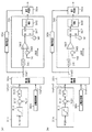
次に、各下位制御部30a,30bの機能を説明する。図2(a)は、第1下位制御部30aを示し、図2(b)は、第2下位制御部30bを示している。第1下位制御部30aと第2下位制御部30bとは基本的には同じ構成であるため、以下では、第1下位制御部30aの機能ブロックのみを詳細に示し、第2下位制御部30bの機能ブロックを適宜省略して説明する。また、以降、各下位制御部30a,30b及び上位制御部40で用いられる第1,第2電流IH1,IH2は、第1,第2電流センサ23a,23bにより検出された第1,第2電流IH1,IH2が一次側コイルL1及び二次側コイルL2の巻数比に応じて変換された値とされている。上記変換された値は、第1,第2DDC10a,10bの出力電流に相当する。
Next, the function of each of the lower control units 30a and 30b will be described. FIG. 2A shows the first lower control unit 30a, and FIG. 2B shows the second lower control unit 30b. Since the first lower control unit 30a and the second lower control unit 30b have basically the same configuration, only the functional blocks of the first lower control unit 30a are shown in detail below, and the second lower control unit 30b The description will be given with the function blocks omitted as appropriate. Hereinafter, the first and second currents IH1 and IH2 used by the lower control units 30a and 30b and the
図2(a)に示すように、第1下位制御部30aは、定電圧制御部31a、定電流制御部32a、最小値選択部33a及びピーク電流制御部34aを備えている。
As shown in FIG. 2A, the first lower control unit 30a includes a constant voltage control unit 31a, a constant
定電圧制御部31aは、第1電圧指令値VL1*に第1出力電圧VL1rをフィードバック制御するための操作量として、第1DDC10aの出力電流の目標値である第1目標電流値Irefcv1を算出する。本実施形態では、上位制御部40から第1下位制御部30aに第1電圧指令値VL1*が出力される。また、上位制御部40から第2下位制御部30bに第2電圧指令値VL2*が出力される。
The constant voltage control unit 31a calculates a first target current value Irefcv1, which is a target value of the output current of the
定電圧制御部31aは、徐変器311、電圧偏差算出器312及びPI制御器313を備えている。まず、第1電圧指令値VL1*は、徐変器311に入力される。徐変器311は、第1電圧指令値VL1*の変化に応じて、この第1電圧指令値VL1*を徐変させた値を出力する。電圧偏差算出器312は、徐変器311により変換された第1電圧指令値VL1*から第1出力電圧センサ22aで検出された第1出力電圧VL1rを減算することにより偏差を算出する。電圧偏差算出器312により算出された偏差は、PI制御器313に入力される。PI制御器313は、入力された偏差に比例積分制御を施すことにより第1目標電流値Irefcv1を算出する。
The constant voltage controller 31a includes a
定電流制御部32aは、第1上限電流値Irefcc1を算出する。本実施形態では、第1上限電流値Irefcc1は第1DDC10aの定格電流(例えば120A)に設定されている。
The constant
最小値選択部33aは、定電圧制御部31aから出力される第1目標電流値Irefcv1と、定電流制御部32aから出力される第1上限電流値Irefcc1とを比較し、いずれか小さい方の値を選択して出力する。そのため、第1目標電流値Irefcv1が第1上限電流値Irefcc1を上回る場合、最小値選択部33aは、第1上限電流値Irefcc1をピーク電流制御部34aへ出力する。以下では、Irefcv1及びIrefcc1の内、最小値選択部33aにより選択された電流値を第1電流指令値Iref1と記載する。
The minimum value selection unit 33a compares the first target current value Irefcv1 output from the constant voltage control unit 31a with the first upper limit current value Irefcc1 output from the constant
ピーク電流制御部34aは、DA変換器341、コンパレータ342及び加算器343を備えている。まず、最小値選択部33aにより選択された第1電流指令値Iref1は、DA変換器341に入力される。DA変換器341は、入力された第1電流指令値Iref1をデジタル値からアナログ値に変換する。アナログ値に変換された第1電流指令値Iref1は、コンパレータ342の反転入力端子に入力される。加算器343は、第1電流IH1とスロープ補償信号とを加算し、補償後スイッチ電流として出力する。加算器343の出力信号は、コンパレータ342の非反転入力端子に入力される。なお、スロープ補償信号は、リアクトル15に流れる電流の変動に伴う発振を抑制するものである。
The peak current control unit 34a includes a
コンパレータ342は、第1電流指令値Iref1と補償後スイッチ電流とを比較し、補償後スイッチ電流が第1電流指令値Iref1より小さい期間において、ロー状態の信号をRSフリップフロップ347のR端子に入力する。また、コンパレータ342は、補償後スイッチ電流が第1電流指令値Iref1より大きい期間において、ハイ状態の信号をRSフリップフロップ347のR端子に入力する。更に、RSフリップフロップ347のS端子には、クロック信号が入力される。RSフリップフロップ347の出力は、デューティ制限部348によってデューティの上限値を設定された上で、第1,第2,第3,第4スイッチQ1,Q2,Q3,Q4をオン・オフするための駆動信号G1,G2,G3,G4として出力される。
The
第1下位制御部30aは、電流判定部35a及び出力判定部36aを備えている。電流判定部35a及び出力判定部36aは、最小値選択部33aにより選択された第1電流指令値Iref1が、第1DDC10aを安定的に動作させることができる電流値を下回る場合に、駆動信号G1〜G4として第1〜第4スイッチQ1〜Q4をオフするオフ駆動信号を出力する。そのため、第1電流指令値Iref1が第1〜第4スイッチQ1〜Q4を安定的に動作させることができないほど小さい場合は、第1〜第4スイッチQ1〜Q4がオフされ、第1DDC10aの動作が停止される。
The first lower control unit 30a includes a
具体的には、電流判定部35aは、最小値選択部33aから出力される第1電流指令値Iref1が所定電流値以下であるか否かを判定する。出力判定部36aは、第1電流指令値Iref1が所定電流値を上回っている旨の判定結果を電流判定部35aから取得した場合、デューティ制限部348から出力された各駆動信号G1〜G4をそのまま第1〜第4スイッチQ1〜Q4のゲートに対して出力する。一方、出力判定部36aは、第1電流指令値Iref1が所定電流値以下である旨の判定結果を電流判定部35aから取得した場合、デューティ制限部348から出力された各駆動信号G1〜G4を全てオフ駆動信号に切り替えて出力する。このため、第1DDC10aの動作が停止される。
Specifically, the
なお、第2下位制御部30bは、図2(b)に示すように、第1下位制御部30aと同様に、定電圧制御部31b、定電流制御部32b、最小値選択部33b、ピーク電流制御部34b、電流判定部35b及び出力判定部36bを備えている。各部31b〜36bの機能は、第1DDC10aが備える各部31a〜36aの機能と同じであるが、入力及び出力される信号が異なる。すなわち、定電圧制御部31bは、第2電圧指令値VL2*に第2出力電圧VL2rをフィードバック制御するための操作量として、出力電流の目標値である第2目標電流値Irefcv2を算出する。また、定電流制御部32bは、第2上限電流値Irefcc2を算出する。本実施形態では、第2上限電流値Irefcc2は第2DDC10bの定格電流(例えば30A)に設定されている。最小値選択部33bは、第2目標電流値Irefcv2と第2上限電流値Irefcc2とを比較し、いずれか小さい方の値を選択して出力する。以下では、Irefcv2及びIrefcc2の内、最小値選択部33aにより選択された電流値を第2電流指令値Iref2と記載する。電流判定部35b及び出力判定部36bは、第2電流指令値Iref2が、第2DDC10bを安定的に動作させることができる電流値を下回る場合に、駆動信号G1〜G4として第2DDC10bの第1〜第4スイッチQ1〜Q4をオフするオフ駆動信号を出力する。
Note that, as shown in FIG. 2B, the second lower control unit 30b includes a constant
次に、第1DDC10a及び第2DDC10bの電力変換効率について説明する。図3は、第1DDC10a及び第2DDC10bそれぞれの出力電流に対する電力変換効率[%]を示す図である。なお、本実施形態では、電力変換システム10の電力変換効率が下式(1)により定義されている。
Next, the power conversion efficiency of the
η=Pout/Pin×100 … (1)
上式(1)において、ηは電力変換効率を示し、0[%]〜100[%]の値である。Poutは、各DDC10a,10bの出力電力を示し、Pinは、各DDC10a,10bの入力電力を示す。
η = Pout / Pin × 100 (1)
In the above equation (1), η indicates the power conversion efficiency, and is a value of 0 [%] to 100 [%]. Pout indicates the output power of each
第1DDC10aは、第2DDC10bと比べて電力変換効率が最大となる負荷が異なっている。図3に示すように、第2DDC10bは、第1負荷領域LA1での電力変換効率が最大となるよう設計され、第1DDC10aは、第1負荷領域LA1よりも負荷が大きい第2負荷領域LA2での電力変換効率が最大となるよう設計されている。また、第1負荷領域LA1の全域において、第2DDC10bの電力変換効率は第1DDC10aの電力変換効率よりも高くなっている。そして、第2負荷領域LA2の全域において、第1DDC10aの電力変換効率は第2DDC10bの電力変換効率よりも高くなっている。
The
本実施形態において、第2DDC10bの定格電流は、第1DDC10aの定格電流よりも小さな値となる。第1負荷領域LA1は、0以上であってかつ第1電流閾値Th11以下の領域に設定され、第1電流閾値Th11は第2DDC10bの定格電流に設定されている。また、第2負荷領域LA2は、第1電流閾値Th11よりも大きくてかつ第2電流閾値Th12以下の領域に設定され、第2電流閾値Th12は第1DDC10aの定格電流よりも小さい値に設定されている。また、第3負荷領域LA3は、第2電流閾値Th12よりも大きい領域に設定されている。
In the present embodiment, the rated current of the
第3負荷領域LA3には、第3電流閾値Th13が設定されている。第3電流閾値Th13は、第2電流閾値Th12よりも大きく、かつ第2DDC10bの定格電流を2倍した値(例えば60A)に設定されている。
A third current threshold Th13 is set in the third load area LA3. The third current threshold Th13 is set to a value (for example, 60 A) that is larger than the second current threshold Th12 and is twice the rated current of the
上位制御部40は、図4に示すように、負荷に応じて第1DDC10a及び第2DDC10bの動作を切り替える。具体的には、第1負荷領域LA1では、第2DDC10bを単独動作させる。第2負荷領域LA2では、第1DDC10aを単独動作させる。そして、第3負荷領域LA3では、第1DDC10aと第2DDC10bとを動作させる。また、この第3負荷領域LA3において、負荷が第2電流閾値Th12よりも大きく、かつ第3電流閾値Th13よりも小さい場合に、第1DDC10aと第2DDC10bとの出力電流を均等化させる均等化制御を実施する。均等化制御により、第1DDC10a及び第2DDC10bの出力電流が同じ値となるよう第1DDC10a及び第2DDC10bが制御される。
The
ここで、第1DDC10a又は第2DDC10bの出力側に断線異常が発生し得る。本実施形態において、第1DDC10aの出力側の断線異常には、第1電気経路LO1と、第2電気経路LO2と、第1出力側配線OUT1において第3出力側配線OUT3との接続箇所よりも第1端子T1側の配線と、第2出力側配線OUT2において第4出力側配線OUT4との接続箇所よりも第2端子T2側の配線とのうち、少なくとも1つが途中で断線することが含まれる。また、第1DDC10aの出力側の断線異常には、第1端子T1から第1出力側配線OUT1がはずれることと、第2端子T2から第2出力側配線OUT2がはずれることとのうち、少なくとも1つが含まれる。また本実施形態において、第2DDC10bの出力側の断線異常には、第3電気経路LO3と、第4電気経路LO4と、第3出力側配線OUT3と、第4出力側配線OUT4とのうち、少なくとも1つが途中で断線することが含まれる。また、第2DDC10bの出力側の断線異常には、第3端子T3から第3出力側配線OUT3がはずれることと、第4端子T4から第4出力側配線OUT4がはずれることとのうち、少なくとも1つが含まれる。
Here, a disconnection abnormality may occur on the output side of the
2台のDDC10a,10bを共通の給電対象である第1蓄電池60に対して並列に接続する構成では、例えば、第1DDC10aの出力側に断線異常が発生しても、断線異常が生じていない第2DDC10bの出力側から第1蓄電池60に対して出力電圧が供給される。そのため、各出力電圧センサ22a、22bにより検出された出力電圧VL1r,VL2rを用いて断線異常を判定する手法では、どちらのDDC10a,10bに断線異常が生じているかの判定が難しい場合がある。そのため、本実施形態では、上位制御部40は、均等化制御で用いる出力補正電圧VLBにより各DDC10a,10bのいずれに断線異常が生じているかを判定する構成としている。
In a configuration in which the two
図5は、電力変換システム10の各部を簡略化して示す回路図である。図5では、第1蓄電池60の端子間電圧をVo、第1DDC10の出力電圧をVL1r、及び第2DDCの出力電圧をVL2rとして示している。また、第1電気経路LO1と、第1出力側配線OUT1のうち第3出力側配線OUT3との接続箇所よりも第1端子T1側の配線との合成抵抗を第1抵抗値R1として示している。また、第3電気経路LO3と、第3出力側配線OUT3との合成抵抗を第2抵抗値R2として示している。なお図5において、RSは、第1出力側配線OUT1のうち第3出力側配線OUT3との接続箇所よりも第1蓄電池60側の配線の抵抗値を示している。ただし本実施形態では、RSがR1,R2と比較して非常に小さい値であるとし、RS≒0としている。
FIG. 5 is a circuit diagram schematically illustrating each unit of the
各DDC10a,10bと第1蓄電池60とを繋ぐ各出力側配線OUT1,OUT3に電流が流れることで電圧降下が生じる。そのため、端子間電圧Vo,出力電圧VL1r,VL2rは下記式(2),(3)で示す関係となる。
VL1r=I1×R1+Vo … (2)
VL2r=I2×R2+Vo … (3)
ここで、I1は第1出力側配線OUT1に流れる電流を示し、I2は第3出力側配線OUT3に流れる電流を示している。
When a current flows through each of the output side wirings OUT1 and OUT3 connecting each of the
VL1r = I1 × R1 + Vo (2)
VL2r = I2 × R2 + Vo (3)
Here, I1 indicates a current flowing through the first output side wiring OUT1, and I2 indicates a current flowing through the third output side wiring OUT3.
上位制御部40が、第1DDC10a及び第2DDC10bの出力電流をI3で均等化するように、出力電圧VL1r,VL2rを出力補正電圧VLBで補正する場合、上記式(2),(3)から、下記式(4),(5)が導出される。
When the higher-
VL1r+VLB=I3×R1+Vo … (4)
VL2r−VLB=I3×R2+Vo … (5)
上記式(4),(5)より、下記式(6)が導出される。
VL1r + VLB = I3 × R1 + Vo (4)
VL2r−VLB = I3 × R2 + Vo (5)
The following equation (6) is derived from the above equations (4) and (5).
VLB=(R1−R2)/2×I3−(VL1r−VL2r)/2 … (6)
上記式(6)より、下記式(7)が導出される。
VLB = (R1-R2) / 2 × I3- (VL1r-VL2r) / 2 (6)
The following equation (7) is derived from the above equation (6).
VLB=(R1−R2)/2×I3+Δoff … (7)
上記式(7)は、出力補正電圧VLBが、各抵抗値R1,R2の差を傾き値として均等化後の電流量I3により変化することを示している。なお、均等化制御の実施下における出力電圧VL1rと出力電圧VL2rとの差を検出ばらつきΔoffとして示している。
VLB = (R1−R2) / 2 × I3 + Δoff (7)
The above equation (7) indicates that the output correction voltage VLB changes according to the equalized current amount I3 using the difference between the resistance values R1 and R2 as a slope value. Note that the difference between the output voltage VL1r and the output voltage VL2r under the execution of the equalization control is shown as a detection variation Δoff.
図6は、横軸を各DDC10a,10bの出力電流の合計値とし、縦軸を出力補正電圧VLBとした場合に、上記式(7)に基づく出力補正電圧VLBの変化を説明する図である。
FIG. 6 is a diagram illustrating a change in the output correction voltage VLB based on the above equation (7), where the horizontal axis is the total value of the output currents of the
各DDC10a,10bの断線異常が生じていない場合、第1出力側配線OUT1の第1抵抗値R1と第3出力側配線OUT3の第2抵抗値R2との差は、所定の範囲となる。そのため、図6では、各DDC10a,10bの断線異常が生じていない場合の出力補正電圧VLBが取り得る変化を正常範囲として規定している。この正常範囲は、上限値LH1及び下限値LH2によって規定される範囲である。そのため、上限値LH1及び下限値LH2は、出力電流が大きいほど大きくなる。
When no disconnection abnormality has occurred in each of the
図6では、出力電流の変化に対する上限値LH1の変化を第1傾き閾値SL1として示しており、出力電流の変化に対する下限値LH2の変化である第2傾き閾値SL2として示している。上限値LH1は下限値LH2よりも傾きが大きいため、第1傾き閾値SL1は第2傾き閾値SL2に対して大きな値となっている。 In FIG. 6, the change of the upper limit LH1 with respect to the change of the output current is shown as the first slope threshold SL1, and the change of the lower limit LH2 with respect to the change of the output current is shown as the second slope threshold SL2. Since the upper limit LH1 has a larger slope than the lower limit LH2, the first slope threshold SL1 is larger than the second slope threshold SL2.
一方、第1DDC10a及び第2DDC10bのいずれかの断線異常が生じている場合、各抵抗値R1,R2のうち断線異常が生じている方に対応する抵抗値が大きくなり、上記式(7)において傾き値(R1−R2)/2を変化させる。具体的には、第1DDC10aの断線異常が生じている場合、第1抵抗値R1が第2抵抗値R2よりも大きくなるため、傾き値(R1−R2)/2をプラス側に変化させる。そのため、図6において、出力補正電圧VLBは、正常範囲よりも高い値となる。また、第2DDC10bの断線異常が生じている場合、第2抵抗値R2が第1抵抗値R1よりも大きくなるため、傾き値(R1−R2)/2をマイナス側に変化させる。そのため、図6において、出力補正電圧VLBは、正常範囲よりも低い値となる。
On the other hand, when any of the
図5,図6で示した特性を用いることにより、均等化制御で用いられる出力補正電圧VLBから、第1DDC10a又は第2DDC10bの断線異常が生じているかを判定することができる。本実施形態では、出力補正電圧VLBの出力電流に対する傾き値を算出し、この傾き値から、第1DDC10a又は第2DDC10bの断線異常を判定する。
By using the characteristics shown in FIGS. 5 and 6, it is possible to determine from the output correction voltage VLB used in the equalization control whether the
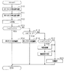
次に、上位制御部40により実施される第1DDC10aと第2DDC10bの動作の切替え処理と断線異常検出処理とを説明する。図7は、上位制御部40が各DDC10a,10bの動作を切り替える切替え処理及び断線異常検出処理を説明するフローチャートである。図7に示すフローチャートは、上位制御部40により所定周期で繰り返し実施される処理である。
Next, a process of switching the operations of the
ステップS10では、第1入力電圧VH1,第1出力電圧VL1r、第1電流IH1を取得する。本実施形態では、第1下位制御部30aが取得した各検出値VH1,VL1r,IH1が上位制御部40に出力されることで、各検出値VH1,VL1r,IH1を取得する。ステップS10が第1出力電流取得部に相当する。
In step S10, the first input voltage VH1, the first output voltage VL1r, and the first current IH1 are obtained. In the present embodiment, the detection values VH1, VL1r, and IH1 acquired by the first lower control unit 30a are output to the
ステップS11では、第2入力電圧VH2,第2出力電圧VL2r、第2電流IH2を取得する。本実施形態では、第2下位制御部30bが取得した各検出値VH2,VL2r,IH2が上位制御部40に出力されることで、各検出値VH2,VL2r,IH2を取得する。ステップS11が第2出力電流取得部に相当する。
In step S11, the second input voltage VH2, the second output voltage VL2r, and the second current IH2 are obtained. In the present embodiment, the detection values VH2, VL2r, and IH2 acquired by the second lower control unit 30b are output to the
ステップS12では、第1蓄電池60への負荷出力としての出力電流Ioを推定する。出力電流Ioは、第1DDC10a及び第2DDC10bのそれぞれから第1蓄電池60へと出力される電流の合計値である。本実施形態では、ステップS10,S11で取得した各検出値と、一次側コイルL1と二次側コイルL2との巻数比とに基づいて、出力電流Ioを推定する。
In step S12, an output current Io as a load output to the
ステップS13,S15では、ステップS12により推定した出力電流Ioが、第1負荷領域LA1に含まれる値であるか、第2負荷領域LA2に含まれる値であるかを判定する。まず、ステップS13では、ステップS12で推定した出力電流Ioが第1電流閾値Th1以下であるか否かを判定する。第1電流閾値Th1は、第1負荷領域LA1と第2負荷領域LA2との境界を区別する値である。 In steps S13 and S15, it is determined whether the output current Io estimated in step S12 is a value included in the first load area LA1 or a value included in the second load area LA2. First, in step S13, it is determined whether the output current Io estimated in step S12 is equal to or less than the first current threshold Th1. The first current threshold Th1 is a value that distinguishes a boundary between the first load area LA1 and the second load area LA2.
なお、第1電流閾値Th1は、第2DDC10bの定格電流に所定のマージンを加えた値としてもよい。この場合において、第1電流閾値Th1は、図3で示す第1DDC10aの電力変換効率が最大となる出力電流よりも大きい値であることが望ましい。
Note that the first current threshold Th1 may be a value obtained by adding a predetermined margin to the rated current of the
ステップS13において、出力電流Ioが第1電流閾値Th1以下であると判定した場合、出力電流Ioが第1負荷領域LA1に含まれると判定し、ステップS14に進む。ステップS14では、第2DDC10bのみを単独動作させる。上位制御部40は、第1電圧指令値VL1*を第2電圧指令値VL2*よりも低い値に設定することで、第2DDC10bのみを単独動作させる。
When it is determined in step S13 that the output current Io is equal to or less than the first current threshold Th1, it is determined that the output current Io is included in the first load region LA1, and the process proceeds to step S14. In step S14, only the
図8は、第2DDC10bを単独動作させる場合に、上位制御部40が実施する各電圧指令値VL1*,VL2*の設定処理を説明する図である。上位電圧指令値VPは、第1DDC10a及び第2DDC10b共に同じ値であり、例えば、第1蓄電池60の定格電圧に応じた電圧(例えば14V)に設定されている。この上位電圧指令値VPは、例えば、上位制御部40に接続された不図示のECUから出力される。
FIG. 8 is a diagram illustrating a setting process of each of the voltage command values VL1 * and VL2 * performed by the
上位制御部40は、上位電圧指令値VPから第1所定値ΔV1(例えば0.5V)を引いた値を第1DDC10aの第1電圧指令値VL1*(例えば13.5V)に設定する。一方、上位制御部40は、上位電圧指令値VPをそのまま第2DDC10bの第2電圧指令値VL2*として設定する。設定された第2電圧指令値VL2*に基づいて第2下位制御部30bの定電圧制御部31bが第2目標電流値Irefcv2を算出することで、第2出力電圧VL2rが第2電圧指令値VL2*に制御される。
The
一方、設定された第1電圧指令値VL1*に基づいて第1下位制御部30aの定電圧制御部31aが第1目標電流値Irefcv1を算出する。ここで、第1電圧指令値VL1*が、第1出力電圧センサ22aにより検出された第1出力電圧VL1rよりも低い値となるため、先の図2の電圧偏差算出器312において、第1出力電圧VL1rと第1電圧指令値VL1*との偏差がマイナスの値となる。そのため、定電圧制御部31aから出力される第1目標電流値Irefcv1は、マイナスの偏差がPI制御器313において比例積分された値となる。この第1目標電流値Irefcv1は、最小値選択部33aにより選択され、第1電流指令値Iref1として電流判定部35aへと出力される。電流判定部35aは、入力された第1電流指令値Iref1が所定電流値以下になると判定する。その結果、出力判定部36aは、デューティ制限部348から出力された各駆動信号G1〜G4を全てオフ駆動信号に切り替えて出力する。これにより、第1DDC10aの動作が停止され、第2DDC10bのみが単独動作する。
On the other hand, the constant voltage control unit 31a of the first lower control unit 30a calculates the first target current value Irefcv1 based on the set first voltage command value VL1 *. Here, since the first voltage command value VL1 * is lower than the first output voltage VL1r detected by the first
先の図7の説明に戻り、ステップS13において出力電流Ioが第1電流閾値Th11を超えていると判定した場合には、ステップS15に進み、出力電流Ioが第2電流閾値Th12以下であるか否かを判定する。第2電流閾値Th12は、第2負荷領域LA2と第3負荷領域LA3とを区別する値である。 Returning to the description of FIG. 7, when it is determined in step S13 that the output current Io exceeds the first current threshold Th11, the process proceeds to step S15, and whether the output current Io is equal to or less than the second current threshold Th12 is performed. Determine whether or not. The second current threshold Th12 is a value that distinguishes the second load region LA2 from the third load region LA3.
なお、第2電流閾値Th12は第1DDC10aの定格電流に所定マージンを加えたに設定されていてもよい。この場合において、第2電流閾値Th12は、図3で示す第1DDC10aの電力変換効率が最大となる出力電流よりも大きい値であることが望ましい。
Note that the second current threshold Th12 may be set to a value obtained by adding a predetermined margin to the rated current of the
ステップS15において出力電流Ioが第2電流閾値Th12以下であると判定した場合には、出力電流が第2負荷領域LA2に含まれると判定し、ステップS16に進む。ステップS16では、第1DDC10aを単独動作させる。具体的には、上位制御部40は、第2電圧指令値VL2*を第1電圧指令値VL1*よりも低い値に設定することで、第1DDC10aを単独動作させる。
If it is determined in step S15 that the output current Io is equal to or smaller than the second current threshold Th12, it is determined that the output current is included in the second load area LA2, and the process proceeds to step S16. In step S16, the
図9は、第1DDC10bを単独動作させる場合に、上位制御部40により実施される各電圧指令値VL1*,VL2*の設定処理を説明する図である。図9においても、上位電圧指令値VPは、例えば、第1蓄電池60の定格電圧に応じた電圧に設定されている。
FIG. 9 is a diagram illustrating a setting process of each of the voltage command values VL1 * and VL2 * performed by the
上位制御部40は、上位電圧指令値VPから第2所定値ΔV2(例えば0.5V)を引いた値を第2DDC10aの第2電圧指令値VL2*(例えば13.5V)に設定する。一方、上位制御部40は、上位電圧指令値VPをそのまま第1DDC10bの第1電圧指令値VL1*として設定する。設定された第1電圧指令値VL1*に基づいて第1DDC10aの定電圧制御部31aが第1目標電流値Irefcv1を算出することで、第1出力電圧VL1rが第1電圧指令値VL1*に制御される。
The
一方、設定された第2電圧指令値VL2*に基づいて第2DDC10bの定電圧制御部31bが第2目標電流値Irefcv2を算出する。ここで、第2電圧指令値VL2*が検出された第2出力電圧VL2rよりも低い値となるため、先の図2の電圧偏差算出器312において、第2出力電圧VL2rと第2電圧指令値VL2*との偏差がマイナスの値となる。そのため、定電圧制御部31bから出力される第2目標電流値Irefcv2は、マイナスの偏差がPI制御器313において比例積分された値となる。この第2目標電流値Irefcv2は、最小値選択部33bにより選択され、第2電流指令値Iref2として電流判定部35bへと出力される。電流判定部35bは、入力された第2電流指令値Iref2が所定電流値以下になると判定する。その結果、出力判定部36bは、デューティ制限部348から出力された各駆動信号G1〜G4を全てオフ駆動信号に切り替えて出力する。これにより、第2DDC10aの動作が停止され、第1DDC10bが単独動作する。
On the other hand, the
先の図7の説明に戻り、ステップS15において出力電流Ioが第2電流閾値Th12を超えていると判定した場合、ステップS17に進み、出力電流Ioが第3電流閾値Th13以下であるか否かを判定する。出力電流Ioが第3電流閾値Th13以下であるため、均等化制御を実施する場合に、第2DDC10bの出力電流を定格電流以下にできる。そのため、ステップS17において出力電流Ioが第3電流閾値Th13以下であると判定した場合には、ステップS18に進み、均等化制御を実施する。
Returning to the description of FIG. 7, when it is determined in step S15 that the output current Io exceeds the second current threshold Th12, the process proceeds to step S17, and whether the output current Io is equal to or less than the third current threshold Th13 is determined. Is determined. Since the output current Io is equal to or less than the third current threshold Th13, the output current of the
図10は、均等化制御を実施する場合の上位制御部40の制御を説明する図である。図10においても、上位電圧指令値VPは、例えば、第1蓄電池60の定格電圧に応じた電圧に設定されている。上位制御部40は、第1電流IH1に、第1電流IH1と第2電流IH2との平均電流値をフィードバック制御するための操作量として出力補正電圧VLBを算出する。そのため、ステップS18が均等化制御部に相当する。
FIG. 10 is a diagram illustrating the control of the higher-
電流偏差算出器401は、出力電流平均値Iave*から第1電流IH1を減算することにより偏差を算出する。ここで、出力電流平均値Iave*は、第1電流センサ23aで検出された第1電流IH1と、第2電流センサ23bで検出された第2電流IH2との平均値である。PI制御器402は、電流偏差算出器401により算出された偏差に基づく比例積分制御により、出力補正電圧VLBを算出する。徐変器403は、PI制御器402により算出された出力補正電圧VLBに徐変処理を施して出力する。第1加算器404は、徐変処理が施された出力補正電圧VLBと上位電圧指令値VPとの加算値を、第1電圧指令値VL1*に設定する。第2加算器405は、徐変処理が施された出力補正電圧VLBの符号反転値と上位電圧指令値VPとの加算値を、第2電圧指令値VL2*に設定する。
The
電流偏差算出器401は、第1DDC10aのトランス13の巻数比に応じて第1電流IH1から算出される出力電流Io1と、出力電流平均値Iave*との偏差を算出するものであってもよい。この場合、出力電流平均値Iave*は、第2DDC10bのトランス13の巻数比に応じて第2電流IH2から算出される出力電流Io2と、出力電流Io1との平均値となる。
The
図10に示す処理によれば、第1電圧指令値VL1*と第2電圧指令値VL2*とは、出力電流を均等化させる値に設定される。これにより、図11に示すように、第1DDC10aの出力電流と第2DDC10bの出力電流とが均等化されて出力される。
According to the processing shown in FIG. 10, the first voltage command value VL1 * and the second voltage command value VL2 * are set to values that equalize the output current. Thereby, as shown in FIG. 11, the output current of the
図7の説明に戻り、ステップS19では、断線異常の判定を行う。本実施形態では、ステップS18で算出した出力補正電圧VLBを用いて、第1DDC10a及び第2DDC10bのいずれかに断線異常が生じているか否かを判定する。ステップS19が断線異常判定部に相当する。
Returning to the description of FIG. 7, in step S19, a disconnection abnormality is determined. In the present embodiment, it is determined whether or not a disconnection abnormality has occurred in any of the
次に、図7のステップS19の詳細な処理を図12のフローチャートを用いて説明する。 Next, the detailed processing of step S19 in FIG. 7 will be described with reference to the flowchart in FIG.
ステップS30では、出力補正電圧VLBの出力電流に対する傾き値Dvlbを算出する。本実施形態では、傾き値Dvlbを、第1電流IH1の変化に対する出力補正電圧VLBの微分値により算出する。ステップS20が傾き値算出部に相当する。傾き値Dvlbは下記式(8)を用いて算出される。
Dvlb=ΔVLB/Δi … (8)
ここで、Δiは、第1電流IH1の変化量を示す。ΔVLBは、第1電流IH1の変化量に対応する出力補正電圧VLBの変化量を示す。
In step S30, a slope value Dvlb with respect to the output current of the output correction voltage VLB is calculated. In the present embodiment, the slope value Dvlb is calculated from the differential value of the output correction voltage VLB with respect to the change in the first current IH1. Step S20 corresponds to a slope value calculation unit. The slope value Dvlb is calculated using the following equation (8).
Dvlb = ΔVLB / Δi (8)
Here, Δi indicates the amount of change in the first current IH1. ΔVLB indicates a change amount of the output correction voltage VLB corresponding to the change amount of the first current IH1.
なお、上位制御部40は、均等化制御の実施下において、出力補正電圧VLBと、この出力補正電圧VLBを算出するのに用いた第1電流IH1とを複数回取得し、これらにより複数の微分値「ΔVLB/Δi」を算出する。そして、算出した複数の微分値「ΔVLB/Δi」の平均値を、傾き値Dvlbとして算出してもよい。また、第1電流IH1の変化量Δiが所定変化以上(主として0以上)であることを条件として、S30の傾き値Dvlbの算出処理を実施してもよい。
Note that the upper-
ステップS31では、ステップS30で算出した傾き値Dvlbを第1傾き閾値SL1と比較する。第1傾き閾値SL1は、図6で示したように正常範囲の上限値SH1の傾き値である。ステップS31において傾き値Dvlbが第1傾き閾値SL1よりも大きいと判定した場合、ステップS32に進む。ステップS32では、第1DDC10aの断線異常が生じていると判定する。これにより、第1DDC10aの断線異常及び第2DDC10bの断線異常のうち、第1DDC10aの断線異常が生じていることを特定できる。
In step S31, the slope value Dvlb calculated in step S30 is compared with a first slope threshold SL1. The first slope threshold SL1 is a slope of the upper limit SH1 of the normal range as shown in FIG. If it is determined in step S31 that the slope value Dvlb is greater than the first slope threshold SL1, the process proceeds to step S32. In step S32, it is determined that the disconnection abnormality of the
ステップS31において傾き値Dvlbが第1傾き閾値SL1以下であると判定した場合、ステップS33に進む。ステップS33では、傾き値Dvlbを第2傾き閾値SL2と比較する。第2傾き閾値SLは、図6で示したように正常範囲の下限値LH2の傾き値である。ステップS33において傾き値Dvlbが第2傾き閾値SL2よりも小さいと判定した場合、ステップS34に進む。ステップS34では、第2DDC10bの断線異常が生じていると判定する。これにより、第1DDC10aの断線異常及び第2DDC10bの断線異常のうち、第2DDC10bの断線異常が生じていることを特定できる。
If it is determined in step S31 that the slope value Dvlb is equal to or less than the first slope threshold SL1, the process proceeds to step S33. In step S33, the slope value Dvlb is compared with a second slope threshold SL2. The second slope threshold SL is a slope of the lower limit LH2 of the normal range as shown in FIG. If it is determined in step S33 that the slope value Dvlb is smaller than the second slope threshold SL2, the process proceeds to step S34. In step S34, it is determined that the disconnection abnormality of the
ステップS33において、傾き値Dvlbが第2傾き閾値SL2以上であると判定した場合、ステップS35に進む。ステップS35では、第1DDC10a及び第2DDC10bの断線異常が共に生じていないと判定する。すなわち、第1DDC10aの出力側と第2DDC10bの出力側とが共に正常であると判定する。
If it is determined in step S33 that the slope value Dvlb is equal to or greater than the second slope threshold SL2, the process proceeds to step S35. In step S35, it is determined that both the
そして、図7の説明に戻り、ステップS17において出力電流Ioが第3電流閾値Th13を超えていると判定した場合には、ステップS20に進む。ステップS20では、第1DDC10aと第2DDC10bとを共同動作させる。本実施形態では、共同動作として、出力電流が定格電流となるよう第2DDC10bを動作させ、かつ第1DDC10aを第1電圧指令値VL1*に応じた出力電圧で動作させる。
Returning to the description of FIG. 7, when it is determined in step S17 that the output current Io exceeds the third current threshold Th13, the process proceeds to step S20. In step S20, the
ステップS14,S16,S19,S20のいずれかの処理を終了した場合、図7の処理を一旦終了する。 When any of the processes in steps S14, S16, S19, and S20 is completed, the process in FIG. 7 is temporarily terminated.
上記構成により、本実施形態に係る電力変換システム10は、以下の効果を奏する。
With the above configuration, the
図13は、出力電圧VL1r,VL2rを用いた断線異常の判定と、本実施形態に係る断線異常の判定の違いを説明する図である。図13では、縦軸に断線異常の判定に必要な各出力側配線OUT1,OUT3の抵抗値を示している。 FIG. 13 is a diagram illustrating the difference between the determination of the disconnection abnormality using the output voltages VL1r and VL2r and the determination of the disconnection abnormality according to the present embodiment. In FIG. 13, the vertical axis indicates the resistance value of each of the output-side wirings OUT1 and OUT3 necessary for determining the disconnection abnormality.
第1DDC10a及び第2DDC10bの出力側配線OUT1,OUT3に生じる出力電圧VL1r,VL2rを用いて断線異常を判定する場合、出力電圧VL1r,VL2rの検出誤差を考慮して、断線異常が生じていない場合と断線異常が生じている場合とで出力電圧VL1r,VL2rの電圧差を所定値以上に設定しておく必要がある。そのため、例えば、第1DDC10a及び第2DDC10bの出力側配線OUT1,OUT3の抵抗値R1,R2を大きな値(例えば、100mΩ)に設定しておく必要がある。
その結果、出力側配線OUT1,OUT3で生じるエネルギー損失が大きくなるといった問題が生じる。
When the disconnection abnormality is determined by using the output voltages VL1r and VL2r generated on the output side wirings OUT1 and OUT3 of the
As a result, there is a problem that energy loss generated in the output side wirings OUT1 and OUT3 increases.
本実施形態では、出力補正電圧VLBを断線異常の判定に用いており、出力側配線OUT1,OUT3の抵抗値R1,R2を大きくする必要がなくなる。そのため、出力側配線OUT1,OUT3で生じるエネルギー損失を低減することができる。また、出力補正電圧VLBを用いて出力側配線OUT1,OUT3の断線異常を判定するため、出力電圧VL1r,VL2rを用いる場合と比べて、断線異常が生じている出力側配線OUT1,OUT3を適正に判定することが可能となる。すなわち、出力側の各抵抗値R1、R2の異常を高精度で検出可能となる。 In the present embodiment, the output correction voltage VLB is used for determining the disconnection abnormality, and it is not necessary to increase the resistance values R1 and R2 of the output-side wirings OUT1 and OUT3. Therefore, energy loss generated in the output side wirings OUT1 and OUT3 can be reduced. In addition, since the disconnection abnormality of the output side wirings OUT1, OUT3 is determined using the output correction voltage VLB, the output side wirings OUT1, OUT3 having the disconnection abnormality are properly compared with the case of using the output voltages VL1r, VL2r. It is possible to make a determination. That is, abnormality of each of the resistance values R1 and R2 on the output side can be detected with high accuracy.
上位制御部40は、出力補正電圧VLBの第1電流IH1に対する傾き値Dvlbを算出し、算出した傾き値Dvlbに基づいて、第1DDC10aの出力側(LO1,LO2,OUT1,OUT2)と第2DDC10bの出力側(LO3,LO4,OUT3,OUT4)とのいずれの断線異常が生じているかを判定する。傾き値Dvlbは、基本的には、断線異常の判定において出力電流の値に対する依存性がない。このため、出力電流の値に関わらず、いずれの出力側に断線異常が生じているかを判定することができる。
The
上位制御部40は、出力側が断線異常でない状態での傾き値を示す傾き閾値SL1,SL2と算出した傾き値Dvlbとの比較により、第1DDC10aの出力側の断線異常と、第2DDC10bの出力側の断線異常とのうち、いずれが生じているかを特定する。上記構成により、傾き値Dvlbと各傾き閾値SL1,SL2との比較という簡易な手法により、第1DDC10aと第2DDC10bとのいずれかの出力側の断線異常を特定することができる。
The
上位制御部40は、第1電流IH1又は第2電流IH2に、第1電流IH1と第2電流IH2との平均値である出力電流平均値Iave*をフィードバック制御するための操作量として出力補正電圧VLBを算出する。上記構成により、第1DDC10aと第2DDC10bの出力電流を均等化させるための出力補正電圧VLBを精度よく算出することができる。
The
(第2実施形態)
第2実施形態では、第1実施形態と異なる構成を中心に説明を行う。
(2nd Embodiment)
In the second embodiment, a description will be given focusing on a configuration different from the first embodiment.
第1DDC10aと第2DDC10bとの双方に断線異常が生じている場合、各出力側の抵抗値R1,R2が共に大きな値となることで、上記式(7)において第1抵抗値R1と第2抵抗値R2との差が小さくなり出力補正電圧VLBが小さな値となる場合がある。このような場合、出力補正電圧VLBの変化が生じにくくなり、傾き値Dvlbが第1傾き閾値SL1より小さく、かつ第2傾き閾値SL2より大きな値となる場合がある。そのため、第1DDC10aと第2DDC10bとの双方に断線異常が生じている場合、出力補正電圧VLBによりこの断線異常を判定できない場合がある。
When the disconnection abnormality has occurred in both the
一方で、第1DDC10aと第2DDC10bとの双方に断線異常が生じている場合、バッテリ補正電圧VLsが異常値となる。そのため、この第2実施形態では、出力補正電圧VLBの変化に加えて、バッテリ補正電圧VLsを用いることで、第1DDC10aと第2DDC10bの出力側の双方が断線異常であることを判定する。
On the other hand, when the disconnection abnormality occurs in both the
図14は、第2実施形態における断線異常の判定を説明するフローチャートである。図14のフローチャートは、図7のステップS19で実施される。なお、ステップS30〜S34の各処理は、図12で示す断線異常の判定と同様であるため、その説明を適宜省略する。 FIG. 14 is a flowchart illustrating the determination of the disconnection abnormality in the second embodiment. The flowchart of FIG. 14 is performed in step S19 of FIG. The processes in steps S30 to S34 are the same as the determination of the disconnection abnormality shown in FIG.
傾き値Dvlbが第2傾き閾値SL2以上であると判定すると(ステップS33:NO)、ステップS40では、バッテリ電圧検出部24により検出された端子間電圧VSrを取得する。ステップS40が端子間電圧取得部に相当する。
If it is determined that the slope value Dvlb is equal to or greater than the second slope threshold SL2 (step S33: NO), in step S40, the terminal voltage VSr detected by the
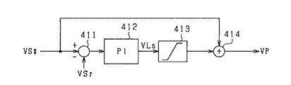
ステップS41では、バッテリ補正電圧VLsを算出する。図15は、上位制御部40の内、第1蓄電池60の端子間電圧VSrを設定するバッテリ電圧指令値VS*に基づいて上位電圧指令値VPを設定する機能を説明する図である。上位制御部40は、バッテリ電圧指令値VS*に端子間電圧VSrをフィードバック制御するための操作量として上位電圧指令値VPを算出する。ステップS41がバッテリ補正電圧算出部に相当する。
In a step S41, a battery correction voltage VLs is calculated. FIG. 15 is a diagram illustrating a function of setting higher-order voltage command value VP based on battery voltage command value VS * that sets terminal-to-terminal voltage VSr of
電圧偏差算出器411は、バッテリ電圧指令値VS*から端子間電圧VSrを減算することにより偏差を算出する。PI制御器412は、電圧偏差算出器411により算出された偏差に基づく比例積分制御により、バッテリ補正電圧VLsを算出する。徐変器413は、PI制御器412により算出されたバッテリ補正電圧VLsに徐変処理を施して出力する。加算器414は、徐変処理が施されたバッテリ補正電圧VLsとバッテリ電圧指令値VS*との加算値を、上位電圧指令値VPに設定する。
上記構成において、第1DDC10aと第2DDC10bとの出力側が共に断線異常である場合、各DDC10a,10bから第1蓄電池60に供給される出力電流が低い値となり、電圧偏差算出器411に加えられる端子間電圧VSrの変化が小さなものとなる。そのため、端子間電圧VSrとバッテリ電圧指令値VS*との偏差が大きくなる。そして、PI制御器412がこの偏差を比例積分してバッテリ補正電圧VLsを算出することで、バッテリ補正電圧は高い値を示す異常値となる。
In the above configuration, when both the output sides of the
ステップS42では、バッテリ補正電圧VLsを補正閾値ThSと比較する。補正閾値ThSは、例えば、第1DDC10aと第2DDC10bとに断線異常が生じていない場合にバッテリ補正電圧VLsが取り得る上限値に設定されていればよい。
In step S42, the battery correction voltage VLs is compared with a correction threshold ThS. The correction threshold ThS may be set to, for example, an upper limit value that the battery correction voltage VLs can take when no disconnection abnormality occurs in the
ステップS42において、バッテリ補正電圧VLsが補正閾値ThSより大きいと判定した場合、ステップS43に進む。ステップS43では、第1DDC10aと第2DDC10bとの双方が断線異常であると判定する。この場合、例えば、上位制御部40は上位のECUに対して電力変換システム10の作動を停止させるよう信号を出力するものであってもよい。
If it is determined in step S42 that the battery correction voltage VLs is higher than the correction threshold ThS, the process proceeds to step S43. In step S43, it is determined that both the
ステップS42において、バッテリ補正電圧VLsが補正閾値ThS以下であると判定した場合、ステップS44に進む。ステップS44では、第1DDC10aの出力側と第2DDC10bの出力側との双方が正常であると判定する。
If it is determined in step S42 that the battery correction voltage VLs is equal to or less than the correction threshold ThS, the process proceeds to step S44. In step S44, it is determined that both the output side of the
ステップS32,S34,S43、S44のいずれかの処理を終了した場合は、図7のフローチャートに戻る。 When any one of steps S32, S34, S43, and S44 is completed, the process returns to the flowchart of FIG.
上記構成により、本実施形態に係る電力変換システム10は、以下の効果を奏する。
With the above configuration, the
出力補正電圧VLBにより断線異常を判定できない場合でも、バッテリ補正電圧VLsが異常であれば、第1DDC10aの出力側と第2DDC10bの出力側との双方が断線異常である可能性が高くなる。上記構成では、上位制御部40は、出力補正電圧VLBに基づいて第1DDC10a及び第2DDC10bの出力側の断線異常を判定しておらず、かつバッテリ補正電圧VLsが補正閾値ThSよりも大きいと判定した場合に、第1DDC10aの出力側と第2DDC10bの出力側との双方が断線異常であると判定することとした。そのため、第1DDC10aの出力側と第2DDC10bの出力側との双方に断線異常が生じている状態を判定でき、断線異常の信頼性を高めることができる。
Even when the disconnection abnormality cannot be determined based on the output correction voltage VLB, if the battery correction voltage VLs is abnormal, it is highly likely that both the output side of the
(第3実施形態)
第3実施形態では、第2実施形態と異なる構成を中心に説明を行う。
(Third embodiment)
In the third embodiment, a description will be given focusing on a configuration different from the second embodiment.
第1DDC10aと第2DDC10bとのいずれかに内部異常が生じていると、出力電圧VL1r,VL2rが異常値となる場合がある。出力電圧VL1r,Vl2rが異常値となることで出力補正電圧VLBの変化を大きくし、上位制御部40がこの出力補正電圧VLBの変化を第1DDC10aの出力側と第2DDC10bの出力側との断線異常として判定してしまうおそれがある。そこで、第3実施形態では、上位制御部40は、第1DDC10a及び第2DDC10bの内部異常を判定し、第1DDC10a及び第2DDC10bに内部異常が生じていないことを条件に、第1DDC10aと第2DDC10bとの断線異常を判定する。
If an internal abnormality occurs in any of the
図16は、第3実施形態にかかる上位制御部40が実施する処理を説明するフローチャートである。図16のフローチャートは、図7のステップS19において上位制御部40により実施される処理である。なお、ステップS30〜S34、及びステップS40〜S44は、図14に示す処理と同様であるため、その説明を適宜省略する。
FIG. 16 is a flowchart illustrating a process performed by the higher-
ステップS42では、バッテリ補正電圧VLsを補正閾値ThSと比較する。ステップS42において、バッテリ補正電圧VLsが補正閾値ThS以下であると判定した場合、ステップS44に進む。ステップS44では、第1DDC10a及び第2DDC10bは共に正常であると判定し、図16の処理を終了する。
In step S42, the battery correction voltage VLs is compared with a correction threshold ThS. If it is determined in step S42 that the battery correction voltage VLs is equal to or less than the correction threshold ThS, the process proceeds to step S44. In step S44, it is determined that both the
一方、ステップS42で、バッテリ補正電圧VLsを補正閾値ThSよりも大きい値であると判定した場合、ステップS51に進む。ステップS51では、第1DDC10a及び第2DDC10bの内部異常が生じているか否かを検出する。内部異常には、例えば、各スイッチQ1〜Q6がオン状態又はオフ状態に固着する異常が含まれる。内部異常の検出手法としては、例えば、各電流センサ23a,23bにより検出される第1電流IH1及び第2電流IH2に基づいて各スイッチQ1〜Q4の故障を検出するものが挙げられる。具体的には、各スイッチQ1〜Q4のいずれかが故障している場合、各電流IH1,IH2の値が変化し、異常値を示す。そのため、上位制御部40は各電流IH1,IH2が電流値の正常値を示す範囲から外れた場合に、第1DDC10a又は第2DDC10bが内部異常であることを検出する。
On the other hand, when it is determined in step S42 that the battery correction voltage VLs is a value larger than the correction threshold ThS, the process proceeds to step S51. In step S51, it is detected whether or not an internal abnormality has occurred in the
ステップS51において、第1DDC10a及び第2DDC10bの少なくとも一方の内部異常を検出した場合、ステップS52に進む。ステップS52では、第1DDC10a及び第2DDC10bの少なくとも一方に内部異常が生じていると判定する。この場合、例えば、上位ECU20に対して内部異常を通知してもよい。ステップS51,S52が内部異常判定部に相当する。
In step S51, when the internal abnormality of at least one of the
ステップS51において、第1DDC10a及び第2DDC10bの少なくとも一方の内部異常を検出していない場合、ステップS43に進む。ステップS43に進む場合、バッテリ補正電圧VLsが補正閾値ThSよりも大きい値と判定しており(ステップS42:YES)、かつ内部異常を判定していない(ステップS51:NO)。そのため、ステップS43では、第1DDC10aの出力側と第2DDC10bの出力側との双方が断線異常であると判定する。
In step S51, when the internal abnormality of at least one of the
ステップS32,S34,S52,S43,S44のいずれかの処理を終了した場合、図7のフローチャートに戻る。 When any one of steps S32, S34, S52, S43, and S44 is completed, the process returns to the flowchart of FIG.
上記構成により、本実施形態に係る電力変換システム10は、以下の効果を奏する。
With the above configuration, the
第1DDC10a及び第2DDC10bに内部異常が生じている場合、出力補正電圧VLBの傾き値の変化がこの内部異常に起因するものか、出力側配線OUT1,OUT2の断線異常に起因するものかが判別しにくくなる。この点、上記構成では、上位制御部40は、第1DDC10a及び第2DDC10bの内部異常を判定する。そして、第1DDC10a及び第2DDC10bの内部異常を判定していないことを条件に、第1DDC10aの出力側と第2DDC10bの出力側との断線異常を判定することとした。そのため、出力補正電圧VLBの異常が第1DDC10a又は第2DDC10bの内部異常に起因するものか、各出力側の断線異常に起因するものかを区別することができ、断線異常の判定精度を高めることができる。
When an internal abnormality has occurred in the
(第4実施形態)
第4実施形態では、第1実施形態と異なる構成を中心に説明を行う。
(Fourth embodiment)
In the fourth embodiment, a description will be given focusing on a configuration different from the first embodiment.
この第4実施形態では、上位制御部40は、電力変換システム10の起動を判定した場合に、均等化制御とこの均等化制御に伴う断線異常の判定とを強制的に実施する。
In the fourth embodiment, when the activation of the
図17は、第4実施形態にかかる上位制御部40が実施する処理を説明するフローチャートである。上位制御部40は図17に示す処理を所定周期で繰り返し実施する。図17では、ステップS10〜S20に示す各処理は、図7で示す各処理と同様であるため、その説明を適宜省略する。
FIG. 17 is a flowchart illustrating a process performed by the higher-
ステップS61では、電力変換システム10の起動の有無を判定する。例えば、電力変換システム10を搭載する車両のイグニッションがオンされることで、不図示のECUから上位制御部40に電力変換システム10を起動させるための起動信号が入力したとする。この場合、電力変換システム10が起動していると判定する。ステップS61が起動判定部に相当する。
In step S61, it is determined whether the
ステップS61において、電力変換システム10の起動を判定した場合、ステップS62に進む。ステップS62では、第1電流IH1を取得する。ステップS63では、第2電流IH2を取得する。
If it is determined in step S61 that the
ステップS64では、第1DDC10a及び第2DDC10bに対して均等化制御を実施する。ステップS64で実施される均等化制御は、図7のステップS18と同様の処理である。ステップS65では、出力補正電圧VLBの傾き値Dvlbを用いて断線異常を判定する。ステップS65で実施される断線異常の判定は、図7のステップS19と同様の処理である。
In step S64, equalization control is performed on the
一方、ステップS61において、電力変換システム10の起動状態を判定しない場合は、ステップS10に進む。ステップS10〜S20では、推定した出力電流Ioに応じて、第1DDC10a及び第2DDC10bの動作を切り替える。そして、均等化制御を実施する場合(ステップS18)、ステップS19では、この均等化制御の実施下において、出力補正電圧VLBに基づいて断線異常を判定する。
On the other hand, when it is determined in step S61 that the
上記構成により、本実施形態に係る電力変換システム10は、以下の効果を奏する。
With the above configuration, the
上位制御部40は、電力変換システム10の起動時において、均等化制御を強制的に実施し、この均等化制御の実施下において、第1DDC10aの出力側及び第2DDC10bの出力側の断線異常を判定することとした。このため、断線異常の有無を判定する機会を適正に確保することができる。
The upper-
(その他の実施形態)
・上位制御部40が均等化制御を実施する際の構成を以下の構成としてもよい。図18〜図20は、均等化制御の他の実施例を示す図である。
(Other embodiments)
The configuration when the higher-
図18,19では、第1DDC10a及び第2DDC10bのいずれかの上位電圧指令値VPのみを、出力補正電圧VLBで補正する。具体的には、図18では、上位制御部40の加算器406は、徐変処理が施された出力補正電圧VLBと上位電圧指令値VPとの加算値を、第1電圧指令値VL1*に設定する。また、上位制御部40は、上位電圧指令値VPをそのまま、第2電圧指令値VL2*に設定する。
18 and 19, only the higher voltage command value VP of one of the
図19では、電流偏差算出器401は、出力電流平均値Iave*から第2電流IH2を減算することにより偏差を算出する。PI制御器402は、電流偏差算出器401により算出された偏差に基づく比例積分制御により、出力補正電圧VLBを算出する。上位制御部40の加算器407は、徐変処理が施された出力補正電圧VLBと上位電圧指令値VPとの加算値を、第2電圧指令値VL2*に設定する。一方、上位制御部40は、上位電圧指令値VPをそのまま、第1電圧指令値VL1*に設定する。
In FIG. 19, the
図20では、電流偏差算出器401は、出力電流平均値Iave*から第2電流IH2を減算することにより偏差を算出する。PI制御器402は、電流偏差算出器401により算出された偏差に基づく比例積分制御により、出力補正電圧VLBを算出する。上位制御部40の第1加算器408は、徐変処理が施された出力補正電圧VLBと上位電圧指令値VPとの加算値を、第2電圧指令値VL2*に設定する。一方、第2加算器409は、徐変処理が施された出力補正電圧VLBの符号反転値と上位電圧指令値VPとの加算値を、第1電圧指令値VL1*に設定する。
In FIG. 20, the
・上位制御部40は、各電流IH1,IH2に基づいて出力電流Ioを推定する以外にも、第1,第2DDC10a,10bの出力電流Ioを直接検出してもよい。この場合、第1,第2DDC10a,10bは、リアクトル15から出力される電流量を検出する電流検出部を備えており、第1,第2下位制御部30a,30bは、電流検出部の検出結果を出力電流として取得し、上位制御部40に出力する。
The
・定電圧制御部31a,31bは、電圧指令値VL*と出力電圧VLrとの偏差を比例積分制御した値に基づいて目標電流値を算出することに代えて、電圧指令値VL*と出力電圧VLrとの偏差を比例制御及び積分制御した値のいずれかに基づいて目標電流値を算出するものであってもよい。
The constant
・上位制御部40が推定する負荷出力としては、第1DDC10a及び第2DDC10bのそれぞれから出力される電力であってもよい。この場合、出力定格値として、定格電流に代えて、定格電力が用いられる。
-The load output estimated by the
・制御装置を、上位制御部40、下位制御部30a,30bにより分割して構成したことは一例に過ぎない。これに代えて、一つの制御部が、上位制御部40及び下位制御部30a,30bの各機能を備える構成であってもよい。
The configuration in which the control device is divided into the
図1において、第2DDC10bと第1蓄電池60とが以下のように接続されていてもよい。第2DDC10bの第3端子T3と繋がる第3出力側配線OUT3が、第1蓄電池60のプラス側端子に接続され、第4端子T4と繋がる第4出力側配線OUT4が第1蓄電池60のマイナス側端子に接続される。この場合において、第1DDC10aの出力側の断線異常には、第1電気経路LO1と、第2電気経路LO2と、第1出力側配線OUT1と、第2出力側配線OUT2とのうち、少なくとも1つが途中で断線することが含まれる。そして、第2DDC10bの出力側の断線異常には、第3電気経路LO3と、第4電気経路LO4と、第3出力側配線OUT3と、第4出力側配線OUT4とのうち、少なくとも1つが途中で断線することが含まれる。
In FIG. 1, the
上位制御部40は、出力補正電圧VLBの傾き値Dvlbに代えて、出力補正電圧VLBを用いて第1DDC10a及び第2DDC10bの断線異常を判定してもよい。この場合、上位制御部40は、出力補正電圧VLBを、図6に示す上限値LH1及び下限値LH2と比較することで、第1DDC10a及び第2DDC10bの断線異常を判定する。具体的には、図12のステップS31において、出力補正電圧VLBが上限値LH1より大きいと判定した場合に、第1DDC10aの出力側の断線異常を判定する。また、図12のステップS33において、出力補正電圧VLBが下限値LH2より小さいと判定した場合に、第2DDC10bの出力側の断線異常を判定する。ここで、断線異常の判定に用いられる上限値LH1及び下限値LH2は、出力電流Ioが大きい程その値が大きく設定されればよい。
The
10…電力変換システム、10a…第1DC/DCコンバータ、10b…第2DC/DCコンバータ、30a,30b…下位制御部、40…上位制御部、60…第1蓄電池。 Reference Signs List 10: power conversion system, 10a: first DC / DC converter, 10b: second DC / DC converter, 30a, 30b: lower control unit, 40: upper control unit, 60: first storage battery.
Claims (7)
出力電流が均等化されるよう前記第1電力変換装置の電圧指令値及び前記第2電力変換装置の電圧指令値の少なくともいずれかを出力補正電圧(VLB)により補正する均等化制御を実施する均等化制御部(S18)と、
前記均等化制御の実施下において、前記出力補正電圧に基づいて、前記第1電力変換装置の出力側(LO1,LO2,OUT1,OUT2)と前記第2電力変換装置の出力側(LO3,LO4,OUT3,OUT4)とのいずれかに断線異常が生じているかを判定する断線異常判定部(S19)と、を備え、
前記第1電力変換装置が前記給電対象に供給する第1出力電流を取得する第1出力電流取得部(S10)と、
前記第2電力変換装置が前記給電対象に供給する第2出力電流を取得する第2出力電流取得部(S11)と、
前記出力補正電圧の前記第1出力電流又は前記第2出力電流の変化に対する傾き値を算出する傾き値算出部(S30)と、を備え、
前記断線異常判定部は、算出した前記傾き値に基づいて、前記第1電力変換装置の出力側と前記第2電力変換装置の出力側とのいずれかに断線異常が生じているかを判定する、電力変換システムの制御装置。 Applied to a power conversion system including a first power conversion device (10a) and a second power conversion device (10b) connected in parallel to a common power supply target (60);
Equalization for performing equalization control for correcting at least one of the voltage command value of the first power converter and the voltage command value of the second power converter using an output correction voltage (VLB) so that the output current is equalized. Conversion control unit (S18);
Under the execution of the equalization control, the output sides (LO1, LO2, OUT1, OUT2) of the first power converter and the output sides (LO3, LO4, LO4) of the second power converter are based on the output correction voltage. OUT3, OUT4), and a disconnection abnormality determination unit (S19) for determining whether a disconnection abnormality has occurred .
A first output current acquisition unit (S10) for acquiring a first output current supplied to the power supply target by the first power conversion device;
A second output current acquisition unit (S11) for acquiring a second output current supplied to the power supply target by the second power conversion device;
A slope value calculator (S30) for calculating a slope value of the output correction voltage with respect to a change in the first output current or the second output current.
The disconnection abnormality determination unit determines whether a disconnection abnormality has occurred on any of the output side of the first power converter and the output side of the second power converter based on the calculated slope value. Control device for power conversion system.
前記第2電力変換装置が前記給電対象に供給する第2出力電流を取得する第2出力電流取得部(S11)と、を備え、
前記均等化制御部は、前記第1出力電流又は前記第2出力電流に、前記第1出力電流と前記第2出力電流との平均電流値をフィードバック制御するための操作量として前記出力補正電圧を算出する、請求項1又は2に記載の電力変換システムの制御装置。 A first output current acquisition unit (S10) for acquiring a first output current supplied to the power supply target by the first power conversion device;
A second output current acquisition unit (S11) for acquiring a second output current supplied to the power supply target by the second power conversion device,
The equalization control unit may control the first output current or the second output current to output the output correction voltage as an operation amount for performing feedback control of an average current value of the first output current and the second output current. The control device of the power conversion system according to claim 1 , wherein the control device calculates.
前記蓄電池の端子間電圧を取得する端子間電圧取得部(S40)と、
バッテリ電圧指令値に前記端子間電圧をフィードバック制御するための操作量として、前記バッテリ電圧指令値を補正するバッテリ補正電圧を算出するバッテリ補正電圧算出部(S41)と、を備え、
前記断線異常判定部は、前記出力補正電圧に基づいて前記第1電力変換装置及び前記第2電力変換装置の出力側の断線異常が生じていると判定しておらず、かつ前記バッテリ補正電圧が異常値であることを判定している場合に、前記第1電力変換装置の出力側と前記第2電力変換装置の出力側との双方に断線異常が生じていると判定する、請求項1〜3のいずれか一項に記載の電力変換システムの制御装置。 The power supply target is a storage battery,
An inter-terminal voltage acquisition unit (S40) for acquiring an inter-terminal voltage of the storage battery;
A battery correction voltage calculation unit (S41) for calculating a battery correction voltage for correcting the battery voltage command value as an operation amount for feedback-controlling the inter-terminal voltage to the battery voltage command value;
The disconnection abnormality determination unit does not determine that a disconnection abnormality on the output side of the first power conversion device and the second power conversion device has occurred based on the output correction voltage, and the battery correction voltage is The method according to claim 1, wherein when it is determined that the output value is an abnormal value, the disconnection abnormality has occurred on both the output side of the first power converter and the output side of the second power converter . 4. The control device for a power conversion system according to claim 3 .
出力電流が均等化されるよう前記第1電力変換装置の電圧指令値及び前記第2電力変換装置の電圧指令値の少なくともいずれかを出力補正電圧(VLB)により補正する均等化制御を実施する均等化制御部(S18)と、Equalization for performing equalization control for correcting at least one of the voltage command value of the first power converter and the voltage command value of the second power converter using an output correction voltage (VLB) so that the output current is equalized. Conversion control unit (S18);
前記均等化制御の実施下において、前記出力補正電圧に基づいて、前記第1電力変換装置の出力側(LO1,LO2,OUT1,OUT2)と前記第2電力変換装置の出力側(LO3,LO4,OUT3,OUT4)とのいずれかに断線異常が生じているかを判定する断線異常判定部(S19)と、を備え、Under the execution of the equalization control, the output sides (LO1, LO2, OUT1, OUT2) of the first power converter and the output sides (LO3, LO4, LO4) of the second power converter are based on the output correction voltage. OUT3, OUT4), and a disconnection abnormality determination unit (S19) for determining whether a disconnection abnormality has occurred.
前記給電対象は蓄電池であって、The power supply target is a storage battery,
前記蓄電池の端子間電圧を取得する端子間電圧取得部(S40)と、An inter-terminal voltage acquisition unit (S40) for acquiring an inter-terminal voltage of the storage battery;
バッテリ電圧指令値に前記端子間電圧をフィードバック制御するための操作量として、前記バッテリ電圧指令値を補正するバッテリ補正電圧を算出するバッテリ補正電圧算出部(S41)と、を備え、A battery correction voltage calculation unit (S41) for calculating a battery correction voltage for correcting the battery voltage command value as an operation amount for feedback-controlling the inter-terminal voltage to the battery voltage command value;
前記断線異常判定部は、前記出力補正電圧に基づいて前記第1電力変換装置及び前記第2電力変換装置の出力側の断線異常が生じていると判定しておらず、かつ前記バッテリ補正電圧が異常値であることを判定している場合に、前記第1電力変換装置の出力側と前記第2電力変換装置の出力側との双方に断線異常が生じていると判定する電力変換システムの制御装置。The disconnection abnormality determination unit does not determine that a disconnection abnormality on the output side of the first power conversion device and the second power conversion device has occurred based on the output correction voltage, and the battery correction voltage is Control of a power conversion system that determines that a disconnection abnormality has occurred on both the output side of the first power conversion device and the output side of the second power conversion device when it is determined that the value is an abnormal value. apparatus.
前記断線異常判定部は、前記第1電力変換装置及び前記第2電力変換装置の出力側の断線異常が生じていると判定しておらず、かつ前記バッテリ補正電圧が前記異常値であることを判定しており、かつ前記内部異常判定部が前記第1電力変換装置及び前記第2電力変換装置の双方に内部異常が生じていると判定していない場合に、前記第1電力変換装置の出力側と前記第2電力変換装置の出力側との双方に断線異常が生じていると判定する、請求項4又は5に記載の電力変換システムの制御装置。 An internal abnormality determining unit (S51, S52) for determining an internal abnormality of the first power converter and the second power converter;
The disconnection abnormality determination unit does not determine that a disconnection abnormality on the output side of the first power conversion device and the second power conversion device has occurred, and that the battery correction voltage is the abnormal value. The output of the first power conversion device when the internal abnormality determination unit has not determined that an internal abnormality has occurred in both the first power conversion device and the second power conversion device. The control device for the power conversion system according to claim 4 , wherein it is determined that a disconnection abnormality has occurred on both the power supply side and the output side of the second power conversion device.
前記均等化制御部は、前記電力変換システムの起動が判定された場合に、前記均等化制御を実施し、
前記断線異常判定部は、前記電力変換システムの起動が判定された場合における前記均等化制御の実施中において、前記出力補正電圧に基づいて、前記第1電力変換装置の出力側と前記第2電力変換装置の出力側とのいずれかに断線異常が生じているかを判定する、請求項1〜6のいずれか一項に記載の電力変換システムの制御装置。 An activation determination unit (S61) for determining that the power conversion system has been activated,
The equalization control unit, when the activation of the power conversion system is determined, performs the equalization control,
The disconnection abnormality determination unit is configured to output the second power and the output side of the first power conversion device based on the output correction voltage during the execution of the equalization control when the activation of the power conversion system is determined. The control device for a power conversion system according to any one of claims 1 to 6, wherein it is determined whether a disconnection abnormality has occurred in any of the output side of the conversion device.
Priority Applications (4)
| Application Number | Priority Date | Filing Date | Title |
|---|---|---|---|
| JP2017016076A JP6634041B2 (en) | 2017-01-31 | 2017-01-31 | Control device for power conversion system |
| PCT/JP2018/002256 WO2018143047A1 (en) | 2017-01-31 | 2018-01-25 | Control device of power conversion system |
| CN201880009118.7A CN110235347B (en) | 2017-01-31 | 2018-01-25 | Control device for power conversion system |
| US16/523,100 US10763669B2 (en) | 2017-01-31 | 2019-07-26 | Power conversion system control device |
Applications Claiming Priority (1)
| Application Number | Priority Date | Filing Date | Title |
|---|---|---|---|
| JP2017016076A JP6634041B2 (en) | 2017-01-31 | 2017-01-31 | Control device for power conversion system |
Publications (3)
| Publication Number | Publication Date |
|---|---|
| JP2018125957A JP2018125957A (en) | 2018-08-09 |
| JP2018125957A5 JP2018125957A5 (en) | 2019-04-25 |
| JP6634041B2 true JP6634041B2 (en) | 2020-01-22 |
Family
ID=63039720
Family Applications (1)
| Application Number | Title | Priority Date | Filing Date |
|---|---|---|---|
| JP2017016076A Active JP6634041B2 (en) | 2017-01-31 | 2017-01-31 | Control device for power conversion system |
Country Status (4)
| Country | Link |
|---|---|
| US (1) | US10763669B2 (en) |
| JP (1) | JP6634041B2 (en) |
| CN (1) | CN110235347B (en) |
| WO (1) | WO2018143047A1 (en) |
Families Citing this family (5)
| Publication number | Priority date | Publication date | Assignee | Title |
|---|---|---|---|---|
| DE102017205481A1 (en) * | 2017-03-31 | 2018-10-04 | Robert Bosch Gmbh | DC converter, power supply and diagnostic method for a DC-DC converter |
| US10978951B2 (en) * | 2017-04-12 | 2021-04-13 | Kyoto University | Passivity-based switching power supply system, controller, and control method |
| JP7257311B2 (en) * | 2019-11-05 | 2023-04-13 | 株式会社デンソー | vehicle charger |
| CN111262448B (en) * | 2020-03-16 | 2021-03-09 | 武汉理工大学 | Full-bridge LLC direct-current charging device and design method thereof |
| CN117129883B (en) * | 2023-10-25 | 2024-02-09 | 广东亿昇达科技有限公司 | Loop control-based battery detection method and device |
Family Cites Families (11)
| Publication number | Priority date | Publication date | Assignee | Title |
|---|---|---|---|---|
| JPH0888971A (en) * | 1994-09-14 | 1996-04-02 | Advantest Corp | Current balance type switching power source |
| JPH08149692A (en) * | 1994-11-18 | 1996-06-07 | Tohoku Oki Denki Kk | Fault detection circuit for dc power supplies connected in parallel |
| JP3052867B2 (en) * | 1997-01-16 | 2000-06-19 | 日本電気株式会社 | Power system |
| JP4379430B2 (en) * | 2006-04-24 | 2009-12-09 | トヨタ自動車株式会社 | Power supply system and vehicle |
| JP5112111B2 (en) * | 2008-03-04 | 2013-01-09 | 株式会社ダイヘン | DC power supply and grid-connected inverter system using this DC power supply |
| JP5202268B2 (en) | 2008-12-11 | 2013-06-05 | 株式会社ダイヘン | Parallel operation type power supply device and control method thereof |
| JP5347795B2 (en) * | 2009-07-21 | 2013-11-20 | 富士通株式会社 | Power supply device, power supply unit diagnosis device, and control method for power supply device |
| JP5634327B2 (en) * | 2011-05-24 | 2014-12-03 | 三菱電機株式会社 | DC / DC converter device |
| CN103311876B (en) * | 2013-06-20 | 2015-09-30 | 华为技术有限公司 | A kind of power supply fuse alarm circuit and alarm device |
| JP5619253B1 (en) * | 2013-10-15 | 2014-11-05 | 三菱電機株式会社 | Inductive load power supply control device |
| JP6369417B2 (en) * | 2015-08-05 | 2018-08-08 | トヨタ自動車株式会社 | Power system |
-
2017
- 2017-01-31 JP JP2017016076A patent/JP6634041B2/en active Active
-
2018
- 2018-01-25 CN CN201880009118.7A patent/CN110235347B/en active Active
- 2018-01-25 WO PCT/JP2018/002256 patent/WO2018143047A1/en active Application Filing
-
2019
- 2019-07-26 US US16/523,100 patent/US10763669B2/en active Active
Also Published As
| Publication number | Publication date |
|---|---|
| CN110235347B (en) | 2020-12-15 |
| JP2018125957A (en) | 2018-08-09 |
| US10763669B2 (en) | 2020-09-01 |
| WO2018143047A1 (en) | 2018-08-09 |
| CN110235347A (en) | 2019-09-13 |
| US20190348837A1 (en) | 2019-11-14 |
Similar Documents
| Publication | Publication Date | Title |
|---|---|---|
| JP6634041B2 (en) | Control device for power conversion system | |
| CN110192336B (en) | Control device and control system for power conversion system | |
| JP6634039B2 (en) | Control device for power conversion system | |
| US9570999B2 (en) | DC-DC converter and DC-DC converter system thereof | |
| KR101682265B1 (en) | Electricity-storage device that can output alternating current | |
| JP6232935B2 (en) | Power supply apparatus and abnormality determination method for power supply apparatus | |
| KR101840412B1 (en) | Buck switch-mode power converter large signal transient response optimizer | |
| JP6192114B2 (en) | Test method and apparatus for transducer | |
| US11228247B2 (en) | Parallel power supply device | |
| CN108897367B (en) | Voltage control circuit, method, apparatus and storage medium | |
| US9780679B2 (en) | Power conversion device and power conversion method | |
| JP6645356B2 (en) | Voltage converter | |
| JP5136394B2 (en) | Vehicle power supply | |
| US11394295B2 (en) | Power supply apparatus | |
| US7336513B1 (en) | Method of compensating output voltage distortion of half-bridge inverter and device based on the method | |
| JP2015177613A (en) | Step-up/down converter device | |
| JP2018099020A (en) | Secondary battery monitoring device and failure diagnosis method | |
| JP2008172862A (en) | Controller of polyphase rotary electric machine | |
| KR20190032682A (en) | System and method for voltage drop compensation control of power supply device | |
| CN109463035A (en) | Power inverter and control method for power inverter | |
| JP6354505B2 (en) | Switching power supply | |
| JP3423196B2 (en) | Inverter circuit | |
| JP4110471B2 (en) | Remote sensing potential detection type vehicle power supply | |
| KR102369338B1 (en) | System and method for auxiliary battery connection status diagnostic | |
| US9444320B1 (en) | Power controller having active voltage balancing of a power supply |
Legal Events
| Date | Code | Title | Description |
|---|---|---|---|
| A521 | Request for written amendment filed |
Free format text: JAPANESE INTERMEDIATE CODE: A523 Effective date: 20190313 |
|
| A621 | Written request for application examination |
Free format text: JAPANESE INTERMEDIATE CODE: A621 Effective date: 20190313 |
|
| TRDD | Decision of grant or rejection written | ||
| A01 | Written decision to grant a patent or to grant a registration (utility model) |
Free format text: JAPANESE INTERMEDIATE CODE: A01 Effective date: 20191119 |
|
| A61 | First payment of annual fees (during grant procedure) |
Free format text: JAPANESE INTERMEDIATE CODE: A61 Effective date: 20191213 |
|
| R150 | Certificate of patent or registration of utility model |
Ref document number: 6634041 Country of ref document: JP Free format text: JAPANESE INTERMEDIATE CODE: R150 |
|
| R250 | Receipt of annual fees |
Free format text: JAPANESE INTERMEDIATE CODE: R250 |
|
| R250 | Receipt of annual fees |
Free format text: JAPANESE INTERMEDIATE CODE: R250 |