JP2015177613A - Step-up/down converter device - Google Patents
Step-up/down converter device Download PDFInfo
- Publication number
- JP2015177613A JP2015177613A JP2014051213A JP2014051213A JP2015177613A JP 2015177613 A JP2015177613 A JP 2015177613A JP 2014051213 A JP2014051213 A JP 2014051213A JP 2014051213 A JP2014051213 A JP 2014051213A JP 2015177613 A JP2015177613 A JP 2015177613A
- Authority
- JP
- Japan
- Prior art keywords
- switch
- signal
- circuit
- output
- input
- Prior art date
- Legal status (The legal status is an assumption and is not a legal conclusion. Google has not performed a legal analysis and makes no representation as to the accuracy of the status listed.)
- Pending
Links
Images


Classifications
-
- H—ELECTRICITY
- H02—GENERATION; CONVERSION OR DISTRIBUTION OF ELECTRIC POWER
- H02M—APPARATUS FOR CONVERSION BETWEEN AC AND AC, BETWEEN AC AND DC, OR BETWEEN DC AND DC, AND FOR USE WITH MAINS OR SIMILAR POWER SUPPLY SYSTEMS; CONVERSION OF DC OR AC INPUT POWER INTO SURGE OUTPUT POWER; CONTROL OR REGULATION THEREOF
- H02M3/00—Conversion of dc power input into dc power output
- H02M3/02—Conversion of dc power input into dc power output without intermediate conversion into ac
- H02M3/04—Conversion of dc power input into dc power output without intermediate conversion into ac by static converters
- H02M3/10—Conversion of dc power input into dc power output without intermediate conversion into ac by static converters using discharge tubes with control electrode or semiconductor devices with control electrode
- H02M3/145—Conversion of dc power input into dc power output without intermediate conversion into ac by static converters using discharge tubes with control electrode or semiconductor devices with control electrode using devices of a triode or transistor type requiring continuous application of a control signal
- H02M3/155—Conversion of dc power input into dc power output without intermediate conversion into ac by static converters using discharge tubes with control electrode or semiconductor devices with control electrode using devices of a triode or transistor type requiring continuous application of a control signal using semiconductor devices only
- H02M3/156—Conversion of dc power input into dc power output without intermediate conversion into ac by static converters using discharge tubes with control electrode or semiconductor devices with control electrode using devices of a triode or transistor type requiring continuous application of a control signal using semiconductor devices only with automatic control of output voltage or current, e.g. switching regulators
- H02M3/158—Conversion of dc power input into dc power output without intermediate conversion into ac by static converters using discharge tubes with control electrode or semiconductor devices with control electrode using devices of a triode or transistor type requiring continuous application of a control signal using semiconductor devices only with automatic control of output voltage or current, e.g. switching regulators including plural semiconductor devices as final control devices for a single load
- H02M3/1582—Buck-boost converters
Abstract
Description
本発明は、太陽光発電等の供給側の入力電圧が変動する電源設備の出力電圧を所定電圧に昇圧又は降圧して出力する昇降圧コンバータ装置に係り、特に自然エネルギーに基づいた昇降圧切換時に発生する不感帯による発電効率の低下を簡素な回路構成で防止することができる昇降圧コンバータ装置に関する。 The present invention relates to a step-up / step-down converter device that outputs an output voltage of a power supply facility in which a supply-side input voltage such as photovoltaic power generation fluctuates to a predetermined voltage, and particularly at the time of step-up / step-down switching based on natural energy. The present invention relates to a buck-boost converter device that can prevent a reduction in power generation efficiency due to a generated dead zone with a simple circuit configuration.
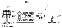
一般に太陽光発電等の供給電力が変化する電源設備において太陽光パネル電圧は、直列接続数や受光光量により大幅に変化することから、入力電圧を所定電圧に昇降圧して出力するための昇降圧コンバータ装置を備える。例えば、図9に示す如く、従来技術による昇降圧コンバータ装置710は、太陽光による直流電圧0V〜600Vの電力を発電する太陽光パネル700に接続され、該太陽光パネル700から出力される0V〜600Vの電圧を0V〜400Vの範囲に昇降圧して出力するように構成されている。
In general, in solar power generation and other power supply facilities where the power supply changes, the solar panel voltage varies greatly depending on the number of serial connections and the amount of received light, so the step-up / down converter for stepping up and down the input voltage to a predetermined voltage for output Equipment. For example, as shown in FIG. 9, a step-up /
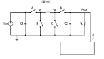
この昇降圧コンバータ装置は、図10に示す如く、太陽光パネルによる入力直流電圧Vinと出力側負荷RLとの間に構成した閉回路の正極側にスイッチAとインダクタとスイッチDとを直列接続し、該閉回路の正極側回路と負極側回路をコンデンサC1又はC2を介して接続する2つの接続回路と、前記スイッチAとインダクタとの間から負極側回路にスイッチBを介して接続する接続回路と、前記インダクタとスイッチDとの間から負極側回路にスイッチCを介して接続する接続回路と、前記スイッチAからDの開閉を制御する制御回路8を備え、スイッチAからDの開閉を制御することによって、該太陽光パネルから出力される電圧を所定の範囲に昇降圧して出力するように構成されている。
In this step-up / down converter apparatus, as shown in FIG. 10, a switch A, an inductor, and a switch D are connected in series on the positive side of a closed circuit formed between an input DC voltage Vin by a solar panel and an output side load RL. , Two connection circuits for connecting the positive-side circuit and the negative-side circuit of the closed circuit via the capacitor C1 or C2, and a connection circuit for connecting the switch A and the inductor to the negative-side circuit via the switch B A connection circuit that connects the inductor and the switch D to the negative circuit via the switch C, and a
上記装置において、昇圧及び降圧動作は入力電圧の値を元に切り替えるため、電圧検出誤差により制御不能となる不感帯が生じ、この電圧付近で所望の動作が得られなくなり、発電効率の低下といった問題が生じる。 In the above device, since the step-up and step-down operations are switched based on the value of the input voltage, there is a dead zone that becomes uncontrollable due to a voltage detection error, and a desired operation cannot be obtained near this voltage, resulting in a problem of a decrease in power generation efficiency. Arise.
上記問題を解決する為に、特許文献1の技術が提案されている。この技術を用いた装置は、図11に示す如く、太陽光パネルによる入力直流電圧Vinと出力側負荷との間に構成した閉回路の正極側にスイッチAとインダクタとスイッチDとを直列接続し、該閉回路の正極側回路と負極側回路をコンデンサC1又はC2を介して接続する2つの接続回路と、前記スイッチAとインダクタとの間から負極側回路にスイッチBを介して接続する接続回路と、前記インダクタとスイッチDとの間から負極側回路にスイッチCを介して接続する接続回路と、前記スイッチAからDの開閉を制御する制御回路80とを備え、該制御回路80が出力側負荷の出力電圧に応じてスイッチAからDの開閉を制御することによって、該太陽光パネルから出力される電圧を所定の範囲に昇降圧して出力するように構成されている。
In order to solve the above problem, the technique of
前記制御回路80は、出力側負荷に供給される出力電圧Voutに接続される抵抗R1及び抵抗R2間の検出電圧をVfbとして負端子に入力し、正端子に目標電圧Vrefを入力し、検出電圧Vfbと目標電圧Vrefとを比較してオンオフ信号VEA1を出力するコンパレータaと、該コンパレータaのオンオフ信号VEA1を負端子に入力し、正端子に所定電圧Vpを入力し、前記オンオフ信号VEA1と所定電圧Vpとを比較してオンオフ信号VEA2を出力するコンパレータbと、前記オンオフ信号VEA1を負端子に入力し、正端子に所定電圧VYを入力とし、オンオフ信号VEA1と所定電圧VYとを比較してオンオフ信号VEA3を出力するコンパレータcと、該コンパレータcからのオンオフ信号VEA3によりスイッチA及びBのオンオフを選択的に切り替える回路素子eと、前記所定電圧VYを180度反転した信号を正端子に入力し、前記コンパレータbからのオンオフ信号VAE2を負端子に入力し、両者を比較してオンオフ信号VEA4を出力するコンパレータdと、該コンパレータdからのオンオフ信号VEA4によりスイッチC及びDのオンオフを選択的に切り替える回路素子fとを備えるように構成されている。
The
このように構成された昇降圧コンバータ装置は、前記制御回路80が、目標電圧(例えば、400V)に対して出力側負荷に供給される出力電圧Voutを監視し、該出力電圧Voutが入力電圧に対して高いときには降圧を行い、低いときには昇圧を行うように降圧動作と昇圧動作を切り替えることによって、原理上は昇降圧の切換時に不感帯が生じることなく、出力電圧を所定範囲(0V〜400Vの範囲)に昇降圧して出力するように動作する。
In the buck-boost converter device configured as described above, the
前記の特許文献1に記載された技術は、出力電圧を監視して所定範囲に昇降圧して出力するものであり、太陽発電のように入力電圧が目標電圧の近傍において変化した際には前記降圧動作と昇圧動作の切り替え動作に不感帯が生じることはないが、反転増幅回路や基準信号生成回路が必要となるなど、回路規模が複雑化するという課題があった。
The technique described in
本発明の目的は、前述の従来技術による課題を解決しようとするものであり、自然エネルギーに基づいた昇降圧切換時に発生する不感帯による発電効率の低下をより簡素な回路構成で防止することができる昇降圧コンバータ装置を提供することである。 An object of the present invention is to solve the above-described problems caused by the prior art, and it is possible to prevent a reduction in power generation efficiency due to a dead zone generated at the time of step-up / step-down switching based on natural energy with a simpler circuit configuration. It is to provide a buck-boost converter device.
前記の目的を達成するために請求項1記載の発明は、昇圧用の複数スイッチと降圧用の複数スイッチのオンオフを切り替えることによって入力電圧を昇降圧して出力するスイッチ回路部と、該スイッチ回路部の入力電圧又は出力電圧と基準信号とを比較した誤差信号に基づいてスイッチ回路部による昇降圧を切り替え制御する制御回路とを備える昇降圧コンバータ装置であって、
該制御回路が、第1の三角波形信号を出力する第1の発振回路と、前記第1三角波形信号と180度位相が異なる第2三角波形信号を出力する第2の発振回路とを備え、第1の三角波形信号及び第2三角波形信号によりデューティ比を規定した降圧パルス信号及び昇圧パルス信号を生成し、該生成した降圧パルス信号及び昇圧パルス信号に基づいてスイッチ回路部の複数スイッチのオンオフ制御を行うことを特徴とする。
In order to achieve the above-described object, the invention according to
The control circuit includes a first oscillation circuit that outputs a first triangular waveform signal, and a second oscillation circuit that outputs a second triangular waveform signal that is 180 degrees out of phase with the first triangular waveform signal; A step-down pulse signal and a step-up pulse signal that define a duty ratio are generated from the first triangular waveform signal and the second triangular waveform signal, and a plurality of switches in the switch circuit unit are turned on and off based on the generated step-down pulse signal and step-up pulse signal. Control is performed.
請求項2記載の発明は、変動する入力直流電圧と出力側負荷の間に構成した閉回路の正極側に第1のスイッチAとインダクタと第4のスイッチD及び第2ダイオードD2の並列回路とを直列接続し、該閉回路の正極側回路と負極側回路を第1又は第2コンデンサC1、C2を介して接続する2つの接続回路と、前記第1スイッチAとインダクタとの間から負極側回路に第2スイッチB及び第1ダイオードD1の並列回路を介して接続する接続回路と、前記インダクタと第4スイッチDとの間から負極側回路に第3スイッチCを介して接続する接続回路と、前記出力側負荷に接続されて前記第1から第4スイッチのオンオフを制御する制御回路とを備え、該制御回路が出力側負荷の出力電圧を監視して第1から第4スイッチのオンオフを制御することによって、前記入力直流電圧を所定の範囲に昇降圧して出力する昇降圧コンバータ装置であって、
前記制御回路が、出力側負荷に供給される出力電圧Voutを負端子に入力し、正端子に基準信号となる目標出力電圧Vrefを入力し、出力電圧Voutと目標出力電圧との差値を増幅して誤差信号として出力する第1増幅器と、第1の三角波形信号を出力する第1発振回路と、前記第1増幅器から出力された誤差信号を正端子に入力し、前記第1発振回路からの第1三角波形信号を負端子に入力し、前記誤差信号と第1三角波形信号とを比較してパルス信号を出力する第1比較器と、前記第1三角波形と180度位相が異なる第2の三角波形信号を出力する第2発振回路と、前記第1増幅器から出力された誤差信号を正端子に入力し、前記第2発振回路からの第2三角波形信号を負端子に入力し、前記誤差信号と第2三角波形信号とを比較してパルス信号を出力する第2比較器と、前記第1比較器及び第2比較器から出力されるパルス信号を入力し、両信号の論理和を第1パルス変調信号として出力する論理素子と、前記論理素子から出力された第1パルス変調信号を反転した第2スイッチ信号を出力する否定素子と、前記第1及び第2比較器から出力されるパルス信号を入力し、両信号の論理積を第3スイッチ信号として出力する論理積素子と、前記論理積素子から出力された第1パルス変調信号を反転して第4スイッチ信号として出力する否定素子とを備え、前記第1パルス変調信号を第1スイッチをオンオフする制御信号とし、前記第2スイッチ信号を第2スイッチをオンオフする制御信号とし、前記第2パルス変調信号を第3スイッチを制御する制御信号とし、前記第4スイッチ信号を第4スイッチをオンオフする制御信号として設定し、降圧動作時においては、第1スイッチ及び第2スイッチを交互にオンオフ並びに第3スイッチをオフ且つ第4スイッチをオンし、昇圧動作時においては、第1スイッチをにオン且つ第2スイッチをオフ並びに第3スイッチ及び第4スイッチを交互にオンオフすることを特徴とする。
According to the second aspect of the present invention, there is provided a parallel circuit of a first switch A, an inductor, a fourth switch D, and a second diode D2 on the positive side of a closed circuit configured between a fluctuating input DC voltage and an output side load. Are connected in series, two connection circuits for connecting the positive side circuit and the negative side circuit of the closed circuit via the first or second capacitor C1, C2, and the negative side from between the first switch A and the inductor. A connection circuit connected to the circuit via a parallel circuit of the second switch B and the first diode D1, and a connection circuit connected between the inductor and the fourth switch D to the negative side circuit via the third switch C; A control circuit connected to the output side load and controlling on / off of the first to fourth switches, and the control circuit monitors the output voltage of the output side load to turn on / off the first to fourth switches. Control It allows the input DC voltage to a buck-boost converter apparatus for elevating pressure and outputs a predetermined range,
The control circuit inputs the output voltage Vout supplied to the output side load to the negative terminal, inputs the target output voltage Vref as a reference signal to the positive terminal, and amplifies the difference value between the output voltage Vout and the target output voltage The first amplifier that outputs the error signal, the first oscillation circuit that outputs the first triangular waveform signal, the error signal output from the first amplifier is input to the positive terminal, and the first oscillation circuit The first triangular waveform signal is input to a negative terminal, the error signal is compared with the first triangular waveform signal, and a pulse signal is output. The first triangular waveform is 180 degrees different in phase from the first triangular waveform. A second oscillation circuit that outputs a triangular waveform signal of 2; an error signal output from the first amplifier is input to a positive terminal; a second triangular waveform signal from the second oscillation circuit is input to a negative terminal; Ratio of the error signal and the second triangular waveform signal A second comparator that outputs a pulse signal and a logic element that receives the pulse signal output from the first comparator and the second comparator and outputs a logical sum of both signals as a first pulse modulation signal; A negative element that outputs a second switch signal obtained by inverting the first pulse modulation signal output from the logic element, and a pulse signal output from the first and second comparators, and a logical product of both signals And a negative element that inverts the first pulse modulation signal output from the AND element and outputs it as a fourth switch signal, and outputs the first pulse modulation signal as a third switch signal. A control signal for turning on and off the first switch; a second control signal for turning on and off the second switch; a second control signal for controlling the third switch; The switch signal is set as a control signal for turning on / off the fourth switch. During the step-down operation, the first switch and the second switch are alternately turned on / off, the third switch is turned off and the fourth switch is turned on. Is characterized in that the first switch is turned on and the second switch is turned off, and the third switch and the fourth switch are alternately turned on and off.
請求項3に記載の発明は、変動する入力直流電圧と出力側負荷の間に構成した閉回路の正極側に第1のスイッチAとインダクタと第4のスイッチD及び第2ダイオードD2の並列回路とを直列接続し、該閉回路の正極側回路と負極側回路を第1又は第2コンデンサC1,C2を介して接続する2つの接続回路と、前記第1スイッチAとインダクタとの間から負極側回路に第2スイッチB及び第1ダイオードD1の並列回路を介して接続する接続回路と、前記インダクタと第4スイッチDとの間から負極側回路に第3スイッチCを介して接続する接続回路と、前記入力直流電圧の電流を検出する電流センサに接続されて前記第1から第4スイッチオンオフAからDを制御する制御回路とを備え、該制御回路が入力電圧を監視して第1から第4スイッチAからDのオンオフを制御することによって、前記入力直流電圧を所定の範囲に昇降圧して出力する昇降圧コンバータ装置であって、
前記制御回路が、前記電流センサにより検出した検出電流を負端子に入力し、正端子に基準信号となる目標出力電圧を入力し、検出電流と目標出力電圧との差値を増幅して誤差信号として出力する増幅器と、第1の三角波形信号を出力する第1発振回路と、前記増幅器から出力された誤差信号を正端子に入力し、前記第1発振回路からの第1三角波形信号を負端子に入力し、該誤差信号と第1三角波形信号とを比較してパルス信号を出力する第1比較器と、前記第1三角波形と180度位相が異なる第2三角波形信号を出力する第2発振回路と、前記増幅器から出力された誤差信号を正端子に入力し、前記第2発振回路からの第2三角波形信号を負端子に入力し、該誤差信号と第2三角波形信号とを比較してパルス信号を出力する第2比較器と、前記第1比較器及び第2比較器から出力されるパルス信号を入力し、両信号の論理和を第1パルス変調信号として出力する論理和素子と、前記論理和素子から出力された第1パルス変調信号を反転した第2スイッチ信号を出力する第1否定素子と、前記第1比較器及び第2比較器から出力される差分信号を入力し、両差分信号の論理積を第3スイッチ信号として出力する論理積素子と、前記論理積素子から出力された第3スイッチ信号を反転した第4スイッチ信号を出力する否定素子とを備え、前記第1パルス変調信号を第1スイッチをオンオフする制御信号とし、前記第2スイッチ信号を第2スイッチをオンオフする制御信号とし、前記第2パルス変調信号を第3スイッチを制御する制御信号とし、前記第4スイッチ信号を第4スイッチをオンオフする制御信号として設定し、降圧動作時においては、第1スイッチ及び第2スイッチを交互にオンオフ並びに第3スイッチをオフ且つ第4スイッチをオンし、昇圧動作時においては、第1スイッチをにオン且つ第2スイッチをオフ並びに第3スイッチ及び第4スイッチを交互にオンオフすることを特徴とする。
According to a third aspect of the present invention, a parallel circuit of a first switch A, an inductor, a fourth switch D, and a second diode D2 is provided on the positive side of a closed circuit configured between a fluctuating input DC voltage and an output side load. Are connected in series, two connection circuits connecting the positive side circuit and the negative side circuit of the closed circuit via the first or second capacitors C1 and C2, and the negative electrode between the first switch A and the inductor. A connection circuit connected to the side circuit via a parallel circuit of the second switch B and the first diode D1, and a connection circuit connected to the negative side circuit via the third switch C from between the inductor and the fourth switch D And a control circuit connected to a current sensor for detecting the current of the input DC voltage and controlling the first to fourth switches on / off A to D, the control circuit monitoring the input voltage and 4th By controlling on and off of D from pitch A, the input DC voltage to a buck-boost converter apparatus for elevating pressure and outputs a predetermined range,
The control circuit inputs a detection current detected by the current sensor to a negative terminal, inputs a target output voltage serving as a reference signal to a positive terminal, amplifies a difference value between the detection current and the target output voltage, and an error signal The first oscillation circuit that outputs the first triangular waveform signal, the error signal output from the amplifier is input to the positive terminal, and the first triangular waveform signal from the first oscillation circuit is negative. A first comparator for inputting a terminal, comparing the error signal with the first triangular waveform signal and outputting a pulse signal, and outputting a second triangular waveform signal that is 180 degrees out of phase with the first triangular waveform. The error signal output from the two oscillation circuit and the amplifier is input to the positive terminal, the second triangular waveform signal from the second oscillation circuit is input to the negative terminal, and the error signal and the second triangular waveform signal are input. Second comparator for comparing and outputting pulse signal A logical sum element for inputting a pulse signal output from the first comparator and the second comparator and outputting a logical sum of both signals as a first pulse modulation signal; and a first output from the logical sum element. A first negative element that outputs a second switch signal obtained by inverting the pulse modulation signal, a difference signal output from the first comparator and the second comparator, and a logical product of both the difference signals are input to a third switch signal. And a negative element that outputs a fourth switch signal obtained by inverting the third switch signal output from the AND element, and controls the first pulse modulation signal to turn on and off the first switch. The second switch signal is a control signal for turning on and off the second switch, the second pulse modulation signal is a control signal for controlling the third switch, and the fourth switch signal is the fourth switch signal. Is set as a control signal for turning on and off, and in the step-down operation, the first switch and the second switch are alternately turned on and off, the third switch is turned off and the fourth switch is turned on, and in the step-up operation, the first switch is turned on. And the second switch is turned off, and the third switch and the fourth switch are alternately turned on and off.
本発明による昇降圧コンバータ装置は、昇圧用の複数スイッチと降圧用の複数スイッチのオンオフを切り替えることによって入力電圧を昇降圧して出力するスイッチ回路部と、該スイッチ回路部の入力電圧又は出力電圧と基準信号とを比較した誤差信号に基づいてスイッチ回路部による昇降圧を切り替え制御する制御回路とを備え、該制御回路が、第1の三角波形信号を出力する第1の発振回路と、前記第1三角波形信号と180度位相が異なる第2三角波形信号を出力する第2の発振回路とを備え、第1の三角波形信号及び第2三角波形信号によりデューティ比を規定した降圧パルス信号及び昇圧パルス信号を生成し、該生成した降圧パルス信号及び昇圧パルス信号に基づいてスイッチ回路部の複数スイッチのオンオフ制御を行うことによって、不感帯による発電効率の低下を簡素回路構成で防止することができる。 A buck-boost converter device according to the present invention includes a switch circuit unit that boosts and outputs an input voltage by switching on and off of a plurality of boosting switches and a plurality of bucking switches, and an input voltage or an output voltage of the switch circuit unit. A control circuit for switching and controlling the step-up / step-down by the switch circuit unit based on an error signal compared with a reference signal, the control circuit outputting a first triangular waveform signal; A step-down pulse signal and a step-up pulse having a duty ratio defined by the first triangular waveform signal and the second triangular waveform signal, and a second oscillation circuit that outputs a second triangular waveform signal that is 180 degrees out of phase with the one triangular waveform signal By generating a pulse signal and performing on / off control of a plurality of switches in the switch circuit unit based on the generated step-down pulse signal and step-up pulse signal. Te, a reduction in power generation efficiency due to the dead zone can be prevented by a simple circuit construction.
また、本発明による昇降圧コンバータ装置は、入力電圧の昇降圧を行うための正極側と負極側を接続する第2スイッチに順方向ダイオードを並列接続すると共に入力直流電圧と出力側負荷の間に構成した閉回路の正極側の第4スイッチに順方向ダイオードを並列接続し、出力電圧又は入力電流を検出する制御回路が、前記出力電圧又は入力電流と目標基準電圧又は目標基準電流との差値に基づく誤差信号に対して位相が180度異なる三角波信号と比較した位相差がある2つのパルス信号を論理和及び論理積した第1パルス変調信号及び第1パルス変調信号と位相が異なる第2パルス変調信号を生成し、降圧動作時には第1パルス変調信号を用いて第1スイッチ及び第2スイッチを交互にオンオフし、昇圧時には第2パルス変調信号を用いて第3スイッチ及び第4スイッチを交互にオンオフすることによって、不感帯による発電効率の低下を簡素回路構成で防止することができる。 In addition, the buck-boost converter device according to the present invention has a forward diode connected in parallel to the second switch that connects the positive electrode side and the negative electrode side for performing step-up / step-down of the input voltage, and between the input DC voltage and the output side load. A control circuit that detects the output voltage or the input current by connecting a forward diode in parallel to the fourth switch on the positive side of the configured closed circuit, and detects a difference value between the output voltage or the input current and the target reference voltage or the target reference current. A first pulse modulation signal obtained by logically and logically ANDing two pulse signals having a phase difference compared to a triangular wave signal that is 180 degrees different in phase with respect to the error signal based on the second pulse having a phase different from that of the first pulse modulation signal A modulation signal is generated. The first switch and the second switch are alternately turned on / off using the first pulse modulation signal during the step-down operation, and the second pulse modulation signal is used during the step-up. By on-off 3 switch and a fourth switch alternately, a reduction in power generation efficiency due to the dead zone can be prevented by a simple circuit construction.
以下、本発明による昇降圧コンバータ方法を適用した昇降圧コンバータ方法装置の一実施形態を図面を参照して詳細に説明する。
[第1実施形態]
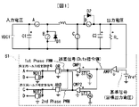
本発明の第1実施形態による昇降圧コンバータ装置は、出力電圧を監視して出力電圧を所定範囲に保つものであって、図1に示す如く、太陽光パネルによる入力直流電圧VDC1と出力側負荷との間に構成した閉回路の正極側にスイッチAとインダクタとスイッチD及びダイオードD2の並列回路とを直列接続し、該閉回路の正極側回路と負極側回路をコンデンサC1又はC2を介して接続する2つの接続回路と、前記スイッチAとインダクタとの間から負極側回路にスイッチB及びダイオードD1の並列回路を介して接続する接続回路と、前記インダクタとスイッチDとの間から負極側回路にスイッチCを介して接続する接続回路を備えるスイッチ回路部と、該スイッチ回路部の出力側負荷RLに接続されて前記スイッチAからDの開閉を制御する制御回路81とを備え、該制御回路81が出力側負荷RLの出力電圧を監視してスイッチAからDの開閉を制御することによって、該太陽光パネルから出力される入力電圧を所定の範囲に昇降圧して出力するように構成されている。
Hereinafter, an embodiment of a buck-boost converter method apparatus to which the buck-boost converter method according to the present invention is applied will be described in detail with reference to the drawings.
[First Embodiment]
The buck-boost converter device according to the first embodiment of the present invention monitors the output voltage and keeps the output voltage within a predetermined range. As shown in FIG. 1, the input DC voltage VDC1 and the output-side load by the solar panel. The parallel circuit of the switch A, the inductor, the switch D, and the diode D2 is connected in series to the positive side of the closed circuit configured between the two and the positive side circuit and the negative side circuit of the closed circuit via the capacitor C1 or C2. Two connecting circuits to be connected, a connecting circuit connected between the switch A and the inductor to the negative side circuit via a parallel circuit of the switch B and the diode D1, and a negative side circuit between the inductor and the switch D A switch circuit section having a connection circuit connected to the switch circuit C via the switch C, and an output side load RL of the switch circuit section to open and close the switches A to D A
前記制御回路81は、出力側負荷RLに供給される出力電圧Voutを負端子に入力し、正端子に基準信号となる目標出力電圧Vrefを入力し、出力電圧Voutと目標出力電圧Vrefとの差値を増幅した誤差信号(Duty指令値)として出力する差分増幅器AMP1と、第1の三角波形(のこぎり波)信号を出力する発振回路ST1と、前記差分増幅器AMP1から出力された誤差信号(Duty指令値)を正端子に入力し、前記発振回路ST1からの第1三角波形信号を負端子に入力し、該誤差信号(Duty指令値)と第1三角波形信号とを比較して誤差信号と基準信号の差がゼロになるようにデューティ比を規定したパルス信号(1st Phase PWM)を出力する比較器CMP1と、前記第1三角波形信号と180度位相が異なる第2三角波形信号を出力する発振回路ST2と、前記差分増幅器AMP1から出力された誤差信号(Duty指令値)を正端子に入力し、前記発振回路ST2からの第2三角波形信号を負端子に入力し、該誤差信号(Duty指令値)と第2三角波形信号とを比較して誤差信号と基準信号の差がゼロになるようにデューティ比を規定したパルス信号(2nd Phase PWM)を出力する比較器CMP2と、前記比較器CMP1及び比較器CMP2から出力されるパルス信号を入力し、両信号の論理和をスイッチ信号Aである降圧用パルス幅変調信号として出力する論理和素子ORと、前記論理和素子ORから出力された降圧用パルス幅変調信号を反転したスイッチ信号Bを出力する否定素子NOT1と、前記比較器CMP1及び比較器CMP2から出力されるパルス信号を入力し、両パルス信号の論理積をスイッチ信号Cである昇圧用パルス幅変調信号として出力する論理積素子ANDと、前記論理積素子ANDから出力された昇圧用パルス幅変調信号を反転してスイッチ信号Dとして出力する否定素子NOT2とを備え、前記スイッチ信号AをスイッチAをオンオフする制御信号、前記スイッチ信号BをスイッチBをオンオフする制御信号、前記スイッチ信号CをスイッチCを制御する制御信号、前記スイッチ信号DをスイッチDをオンオフする制御信号として使用するように構成されている。
The
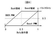
このように構成された第1実施形態による昇降圧コンバータ装置は、誤差信号(Duty指令値)に対して位相が180度異なる第1三角波信号及び第2三角波信号を用いてデューティ比を規定した2つのパルス幅変調(PWM:PULSE WIDTH MODULATION)したパルス信号を生成し、図6に示した2つのパルス信号の論理和(OR)であるBUCK PWMを降圧用パルス幅変調信号(Buck PWM)として使用し、2つのパルス幅変調信号の論理積(AND)であるBoost PWMを昇圧用パルス幅変調信号(Boost PWM)として使用し、Duty(デューティ)指令値が0.5未満においては2つのパルス幅変調信号が同時にオンとならないため、昇圧(Boost)PWMのDuty指令値は常に値「0」であり、Duty指令値の2倍に比例した降圧(BUCK)PWMが生成され、Duty指令値が0.5以上においては2つのパルス幅変調信号が同時にオンとなる期間が発生して降圧(BUCK)Duty指令値が常値に「1」となり、Duty指令値の2倍に比例した昇圧(Boost)PWMが生成される。 The buck-boost converter device according to the first embodiment configured as described above defines a duty ratio using a first triangular wave signal and a second triangular wave signal that are 180 degrees out of phase with respect to an error signal (Duty command value). Two pulse width modulated (PWM: PULSE WIDTH MODULATION) pulse signals are generated, and BUCK PWM, which is the logical sum (OR) of the two pulse signals shown in FIG. 6, is used as a step-down pulse width modulated signal (Buck PWM). Boost PWM, which is the logical product (AND) of the two pulse width modulation signals, is used as the boost pulse width modulation signal (Boost PWM), and when the duty command value is less than 0.5, the two pulse widths are used. Since the modulation signals are not turned on at the same time, the boost PWM boost command value is always the value. A step-down (BUCK) PWM that is “0” and proportional to twice the duty command value is generated, and when the duty command value is 0.5 or more, there is a period in which the two pulse width modulation signals are simultaneously turned on. The step-down (BUCK) duty command value becomes “1” to the normal value, and a boost PWM that is proportional to twice the duty command value is generated.
本実施形態による昇降圧コンバータ装置は、発振回路ST1及びST2の位相が180度異なる2つの三角波信号を発生し、この2つの三角波信号と誤差信号(Duty値)とを比較器CMP1及びCMP2が比較して変調されたパルス信号である1stPhasePWMと2ndPhasePWMとを出力し、スイッチ信号AからDがスイッチAからDのオンオフを制御し、図2に示す如く、降圧動作時においては、スイッチA及びBが交互にオンオフし且つスイッチCは常にオフ、スイッチDは常にオンとなり、昇圧動作時においては、スイッチAは常にオン、スイッチBは常にオフし且つスイッチC及びDが交互にオンオフすることによって、反転増幅回路や基準信号生成回路が必要となるなどの回路規模の複雑化を招くことなく昇降圧を制御することができる。 The buck-boost converter device according to the present embodiment generates two triangular wave signals whose phases of the oscillation circuits ST1 and ST2 are 180 degrees different, and the comparators CMP1 and CMP2 compare the two triangular wave signals with an error signal (Duty value). 1stPhasePWM and 2ndPhasePWM, which are modulated pulse signals, are output, and switch signals A to D control the on / off of switches A to D. As shown in FIG. Inverted by alternately turning on and off, switch C is always off, switch D is always on, and switch A is always on, switch B is always off and switches C and D are alternately turned on and off during the boost operation. Ascending and descending without complicating the circuit scale, such as the need for an amplifier circuit and reference signal generation circuit It is possible to control the.
[第2実施形態]
前述の実施形態においては、出力電圧を監視して降圧及び昇圧を制御する電圧監視制御を行う例を説明したが、本発明による昇降圧コンバータ装置は、入力側の電流を監視して降圧及び昇圧を制御する電流監視制御を行うことができ、この実施形態を図3及び図4を参照して説明する。
[Second Embodiment]
In the above-described embodiment, the example of performing the voltage monitoring control for monitoring the output voltage and controlling the step-down and step-up has been described. However, the step-up / step-down converter device according to the present invention monitors the input side current and performs step-down and step-up. This embodiment will be described with reference to FIGS. 3 and 4. FIG.
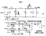
本実施形態による昇降圧コンバータ装置は、図3に示す如く、入力電流を監視して所定範囲に保つものであって、図3に示す如く、太陽光パネルによる入力直流電圧VDC1と出力側負荷との間に電流センサSを介して構成した閉回路の正極側にスイッチAとインダクタとスイッチD及びダイオードD2の並列回路とを直列接続し、該閉回路の正極側回路と負極側回路をコンデンサC1又はC2を介して接続する2つの接続回路と、前記スイッチAとインダクタとの間から負極側回路にスイッチB及びダイオードD1の並列回路を介して接続する接続回路と、前記インダクタとスイッチDとの間から負極側回路にスイッチCを介して接続する接続回路を備えるスイッチ回路部と、該スイッチ回路部の入力直流電圧VDC1の電流を検出する電流センサSに接続されて前記スイッチAからDの開閉を制御する制御回路82とを備え、該制御回路82が電流センサSに流れる入力電流を監視してスイッチAからDの開閉を制御することによって、該太陽光パネルから出力される入力電圧を所定の範囲に昇降圧して出力するように構成されている。
The buck-boost converter device according to the present embodiment monitors the input current and keeps it within a predetermined range as shown in FIG. 3, and as shown in FIG. 3, the input DC voltage VDC1 and the output side load by the solar panel A switch A, an inductor, a parallel circuit of a switch D, and a diode D2 are connected in series to the positive side of the closed circuit configured via the current sensor S between the positive circuit and the negative side circuit of the closed circuit. Or two connection circuits connected via C2, a connection circuit connected between the switch A and the inductor to the negative side circuit via a parallel circuit of the switch B and the diode D1, and the inductor and the switch D. A switch circuit unit having a connection circuit connected to the negative-side circuit via the switch C from the gap, and an electric current for detecting the current of the input DC voltage VDC1 of the switch circuit unit
前記制御回路82は、前記電流センサSにより検出した検出電流を負端子に入力し、正端子に基準信号となる目標入力電流Vrefを入力し、検出電流と目標入力電流Vrefとの差値を増幅して誤差信号(Duty指令値)として出力する差分増幅器AMP1と、第1の三角波形信号を出力する発振回路ST1と、前記差分増幅器AMP1から出力された誤差信号(Duty指令値)を正端子に入力し、前記発振回路ST1からの第1三角波形信号(のこぎり波)を負端子に入力し、該誤差信号(Duty指令値)と第1三角波形信号とを比較して誤差信号と基準信号の差がゼロになるようにデューティ比を規定したパルス信号(1st Phase PWM)を出力する比較器CMP1と、前記第1三角波形と180度位相が異なる第2三角波形信号を出力する発振回路ST2と、前記差分増幅器AMP1から出力された誤差信号Duty指令値)を正端子に入力し、前記発振回路ST2からの第2三角波形信号を負端子に入力し、該誤差信号(Duty指令値)と第2三角波形信号とを比較して誤差信号と基準信号の差がゼロになるようにデューティ比を規定したパルス信号(2nd Phase PWM)を出力する比較器CMP2と、前記比較器CMP1及び比較器CMP2から出力されるパルス信号を入力し、両パルス信号の論理和をスイッチ信号Aである降圧用パルス幅変調信号(Buck PWM)として出力する論理和素子ORと、前記論理和素子ORから出力されたスイッチ信号Aを反転したスイッチ信号Bを出力する否定素子NOT1と、前記比較器CMP1及び比較器CMP2から出力される差分信号を入力し、両差分信号の論理積をスイッチ信号Cである昇圧用パルス幅変調信号(Boost PWM)として出力する論理積素子ANDと、前記論理積素子ANDから出力されたスイッチ信号Cを反転したスイッチ信号Dを出力する否定素子NOT2とを備え、前記第1パルス変調信号をスイッチAをオンオフする制御信号、前記スイッチ信号BをスイッチBをオンオフする制御信号、前記第2パルス変調信号をスイッチCを制御する制御信号、前記スイッチ信号DをスイッチDをオンオフする制御信号として使用するように構成されている。
The
このように構成された第2実施形態による昇降圧コンバータ装置は、入力電流に基づいた誤差信号(Duty指令値)に対して位相が180度異なる第1三角波信号及び第2三角波信号を用いて2つのパルス幅変調(PWM:PULSE WIDTH MODULATION)信号を生成し、第1実施形態同様に、図6に示した第1パルス変調信号(1stPhasePWM)及び第2パルス変調信号(2ndPhasePWM)を生成する。 The buck-boost converter device according to the second embodiment configured as described above uses the first triangular wave signal and the second triangular wave signal that are 180 degrees out of phase with respect to the error signal (Duty command value) based on the input current. Two pulse width modulation (PWM: PULSE WIDTH MODULATION) signals are generated, and the first pulse modulation signal (1stPhasePWM) and the second pulse modulation signal (2ndPhasePWM) shown in FIG. 6 are generated as in the first embodiment.
本実施形態による昇降圧コンバータ装置においても、発振回路ST1及びST2が位相が180度異なる2つの三角波信号を発生し、この2つの三角波信号と入力電流に基づいた誤差信号(Duty指令値)とを比較器CMP1及びCMP2が比較して1stPhasePWMと2ndPhasePWMとを出力し、スイッチ信号AからDがスイッチAからDのオンオフを制御し、図4に示す如く、降圧動作時においては、スイッチA及びBが交互にオンオフし且つスイッチCは常にオフ、スイッチDは常にオンとなり、昇圧動作時においては、スイッチAは常にオン、スイッチBは常にオフし且つスイッチC及びDが交互にオンオフすることによって、反転増幅回路や基準信号生成回路が必要となるなどの回路規模の複雑化を招くことなく昇降圧を制御することができる。 Also in the buck-boost converter device according to the present embodiment, the oscillation circuits ST1 and ST2 generate two triangular wave signals whose phases are different by 180 degrees, and the two triangular wave signals and an error signal (Duty command value) based on the input current are generated. Comparators CMP1 and CMP2 compare to output 1stPhasePWM and 2ndPhasePWM, and switch signals A to D control the on / off of switches A to D. As shown in FIG. Inverted by alternately turning on and off, switch C is always off, switch D is always on, and switch A is always on, switch B is always off and switches C and D are alternately turned on and off during the boost operation. Without complicating the circuit scale, such as the need for an amplifier circuit or reference signal generation circuit It is possible to control the buck.
[第3実施形態]
前記実施形態による昇降圧コンバータ装置の回路構成は、入力電圧又は出力電圧をフィードバックした基本的回路構成を示したものであるが、実際の回路構成は、プログラミングによって入力信号に対する出力信号を設定することができるマイクロコンピュータを使用して回路を構成することが望ましく、このマイクロコンピュータを用いた第3の実施形態を次に説明する。
[Third Embodiment]
The circuit configuration of the buck-boost converter device according to the above embodiment shows a basic circuit configuration in which the input voltage or the output voltage is fed back, but the actual circuit configuration sets the output signal for the input signal by programming. It is desirable to construct a circuit using a microcomputer capable of performing the above, and a third embodiment using this microcomputer will be described next.
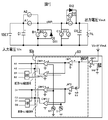
この第3の実施形態よる昇降圧コンバータ装置は、図7に示す如く、前述の実施形態におけるスイッチ回路部におけるスイッチAからスイッチDを、各スイッチを多段に並列配置したスイッチA1及びA2とスイッチB1及びB2とスイッチC1及びC2とスイッチD1及びD2とに変更すると共に、制御回路83における破線で示した部分83aをプログラミングによって入力信号に対する出力信号を設定することができるマイクロコンピュータによって構成している。
As shown in FIG. 7, the step-up / step-down converter device according to the third embodiment includes switches A1 to A2 and switches B1 in which the switches A to D in the switch circuit section in the above-described embodiment are arranged in parallel. And B2, switches C1 and C2, and switches D1 and D2, and a
この制御回路83は、スイッチ回路部からの入力電圧Vin又は出力電圧Voutを入力として降圧動作と昇圧動作を切り替えるものであって、前記入力電圧Vin又は出力電圧Voutを基準信号Vrefと比較して差異を誤差信号(Duty指令値)を出力する差分増幅器AMP1と、この入力した誤差信号(Duty指令値)に基づいた前記複数のスイッチのオンオフを制御する降圧用パルス幅変調信号(Buck PWM)及び昇圧用パルス幅変調信号(Boots PWM)を出力するマイクロコンピュータ83aと、該降圧用パルス幅変調信号(Buck PWM)の位相をシフトすることにより図8に示した位相が異なる降圧用のパルス信号であるスイッチ信号A1,A2,B1,B2を出力し、昇圧用パルス幅変調信号(Boots PWM)の位相をシフトすることにより図8に示した位相が異なる降圧用のパルス信号であるスイッチ信号C1,C2,D1,D2を出力する論理回路素子(LOGIC)とを備える。
The
前記マイクロコンピュータ83aは、プログラミングによって、前記差分増幅器AMP1から出力された誤差信号(Duty指令値)を正端子に入力し、誤差信号が設定された範囲内にあるときには誤差信号に対して線形出力し、設定範囲を超えたとき設定値以上にならない出力信号を出力するリミッタ回路LMT1と、前記差分増幅器AMP1から出力された誤差信号(Duty指令値)を0.5増幅して正端子に入力し、入力信号が設定された範囲内にあるときには誤差信号に対して線形出力し、設定範囲を超えたとき設定値以上にならない出力信号を出力するリミッタ回路LMT2と、第1の三角波形(のこぎり波)信号を出力する発振回路ST1と、前記第1三角波形信号と180度位相が異なる第2三角波形信号を出力する発振回路ST2と、前記リミッタ回路LMT1の出力信号を正端子に入力し負端子に発振回路ST1の第1の三角波形(のこぎり波)信号を入力し、差分値を出力する比較回路CMP1−1と前記リミッタ回路LMT1の出力信号を正端子に入力し負端子に発振回路ST2の第2の三角波形(のこぎり波)信号を入力し、差分値を出力する比較回路CMP1−2と、前記リミッタ回路LMT2の出力信号を正端子に入力し負端子に発振回路ST1の第1の三角波形(のこぎり波)信号を入力し、差分値を出力する比較回路CMP2−1と、前記リミッタ回路LMT2の出力信号を正端子に入力し負端子に発振回路ST2の第2の三角波形(のこぎり波)信号を入力し、差分値を出力する比較回路CMP2−2とを構成している。
The
本実施形態による昇降圧コンバータ装置は、誤差信号(Duty指令値)が0.5〜1の範囲においてはリミッタ回路LMT1が降圧動作を行うための降圧パルス信号を生成し、リミッタ回路LMT2が誤差信号0〜0.5未満の範囲において昇圧動作を行うための昇圧パルス信号を生成し、図8に示す如く、発振回路ST1及びST2からの位相が180度異なる2つの三角波信号を用いて降圧パルス信号により主にスイッチA1,A2,B1,B2を位相をずらしながらオンオフするスイッチ信号A1,A2,B1,B2を生成して降圧動作を行う(スイッチ信号D2のみはオンを維持)と共に、発振回路ST1及びST2からの位相が180度異なる2つの三角波信号を用いて昇圧パルス信号により主にスイッチC1,C2,D1,D2を位相をずらしながらオンオフするスイッチ信号C1,C2,D1,D2を生成して降圧動作を行う(スイッチ信号A1,A2はオンオフ)ように動作することによって、反転増幅回路や基準信号生成回路が必要となるなどの回路規模の複雑化を招くことなく昇降圧を制御することができる。 The buck-boost converter device according to the present embodiment generates a step-down pulse signal for the limiter circuit LMT1 to perform a step-down operation when the error signal (Duty command value) is in the range of 0.5 to 1, and the limiter circuit LMT2 generates the error signal. A step-up pulse signal for performing a step-up operation in the range of less than 0 to 0.5 is generated, and the step-down pulse signal is generated using two triangular wave signals whose phases from the oscillation circuits ST1 and ST2 are different by 180 degrees as shown in FIG. Therefore, switch signals A1, A2, B1, and B2 that turn on and off the switches A1, A2, B1, and B2 while shifting the phase are generated to perform a step-down operation (only the switch signal D2 is kept on), and the oscillation circuit ST1 And the switches C1, C2, D1, D mainly by the boost pulse signal using two triangular wave signals whose phases from ST2 are 180 degrees different from each other. Is generated by generating switch signals C1, C2, D1, and D2 that are turned on and off while shifting the phase of the signal and performing a step-down operation (switch signals A1 and A2 are turned on and off), thereby requiring an inverting amplifier circuit and a reference signal generation circuit. The buck-boost can be controlled without complicating the circuit scale.
このように本発明による昇降圧コンバータ装置は、複数のスイッチをオンオフすることによって入力電圧を昇降圧して出力するスイッチ回路部と、該スイッチ回路部の入力電圧又は出力電圧と基準信号とを比較した誤差信号(Duty指令値)が基準信号に基づいてスイッチ回路部による昇降圧を切り替え制御する制御回路とを備え、該制御回路が、第1の三角波形信号及び第2三角波形信号により誤差信号(Duty指令値)と基準信号の差がゼロになるようにデューティ比を規定した降圧パルス信号及び昇圧パルス信号を生成し、該生成した降圧パルス信号及び昇圧パルス信号に基づいてスイッチ回路部の複数スイッチのオンオフ制御を行うことによって、反転増幅回路や基準信号生成回路が必要となるなどの回路規模の複雑化を招くことなく昇降圧を制御することができる。 As described above, the buck-boost converter device according to the present invention compares the input voltage or output voltage of the switch circuit section with the reference signal, and the switch circuit section that boosts and outputs the input voltage by turning on and off the plurality of switches. And an error signal (Duty command value) including a control circuit for switching and controlling the step-up / step-down by the switch circuit unit based on the reference signal, and the control circuit uses the first triangular waveform signal and the second triangular waveform signal as an error signal ( A step-down pulse signal and a step-up pulse signal that define a duty ratio so that a difference between the duty command value) and the reference signal becomes zero, and a plurality of switches in the switch circuit unit based on the generated step-down pulse signal and step-up pulse signal The on / off control of the circuit may complicate the circuit scale, such as requiring an inverting amplifier circuit and a reference signal generation circuit. It can be controlled without buck.
このように本発明の実施形態による昇降圧コンバータ装置は、図5に示す如く、入力電圧が0Vから600Vの間で変化したとき、入力電圧が出力電圧より大きい状態においては、Duty指令値が0から0.5まで連続的に増加し、入力電圧が出力電圧より小さい状態においては、Duty指令値が0.5から1.0まで連続的に増加することによって、Duty指令値が安定動作(定常動作)ラインと一致する様に変化し、不感帯の発生を防止し、回路規模の複雑化を招くことなく昇降圧を制御することができる。 Thus, in the buck-boost converter device according to the embodiment of the present invention, when the input voltage changes between 0V and 600V, the duty command value is 0 when the input voltage is larger than the output voltage, as shown in FIG. When the input voltage is continuously lower from 0.5 to 1.0 and the input voltage is smaller than the output voltage, the duty command value continuously increases from 0.5 to 1.0. It is possible to control the step-up / step-down without increasing the complexity of the circuit scale by preventing the generation of the dead zone.
80及び81 制御回路、700 太陽光パネル、
710 昇降圧コンバータ装置、AからD スイッチ、S 電流センサ、
ST1及びST2 発振回路、CMP1及びCMP2 比較器
80 and 81 control circuit, 700 solar panel,
710 Buck-Boost converter device, A to D switch, S current sensor,
ST1 and ST2 oscillation circuit, CMP1 and CMP2 comparator
Claims (3)
該制御回路が、第1の三角波形信号を出力する第1の発振回路と、前記第1三角波形信号と180度位相が異なる第2三角波形信号を出力する第2の発振回路とを備え、第1の三角波形信号及び第2三角波形信号によりデューティ比を規定した降圧パルス信号及び昇圧パルス信号を生成し、該生成した降圧パルス信号及び昇圧パルス信号に基づいてスイッチ回路部の複数スイッチのオンオフ制御を行うことを特徴とする昇降圧コンバータ装置。 A switch circuit unit that boosts and outputs an input voltage by switching on and off of a plurality of step-up switches and a plurality of step-down switches, and an error signal that compares the input voltage or output voltage of the switch circuit unit with a reference signal A step-up / down converter apparatus comprising a control circuit for switching and controlling the step-up / step-down by the switch circuit unit,
The control circuit includes a first oscillation circuit that outputs a first triangular waveform signal, and a second oscillation circuit that outputs a second triangular waveform signal that is 180 degrees out of phase with the first triangular waveform signal; A step-down pulse signal and a step-up pulse signal that define a duty ratio are generated from the first triangular waveform signal and the second triangular waveform signal, and a plurality of switches in the switch circuit unit are turned on and off based on the generated step-down pulse signal and step-up pulse signal. A buck-boost converter device characterized by performing control.
前記制御回路が、出力側負荷に供給される出力電圧Voutを負端子に入力し、正端子に基準信号となる目標出力電圧Vrefを入力し、出力電圧Voutと目標出力電圧との差値を増幅して誤差信号として出力する第1増幅器と、第1の三角波形信号を出力する第1発振回路と、前記第1増幅器から出力された誤差信号を正端子に入力し、前記第1発振回路からの第1三角波形信号を負端子に入力し、前記誤差信号と第1三角波形信号とを比較してパルス信号を出力する第1比較器と、前記第1三角波形と180度位相が異なる第2の三角波形信号を出力する第2発振回路と、前記第1増幅器から出力された誤差信号を正端子に入力し、前記第2発振回路からの第2三角波形信号を負端子に入力し、前記誤差信号と第2三角波形信号とを比較してパルス信号を出力する第2比較器と、前記第1比較器及び第2比較器から出力されるパルス信号を入力し、両信号の論理和を第1パルス変調信号として出力する論理素子と、前記論理素子から出力された第1パルス変調信号を反転した第2スイッチ信号を出力する否定素子と、前記第1及び第2比較器から出力されるパルス信号を入力し、両信号の論理積を第3スイッチ信号として出力する論理積素子と、前記論理積素子から出力された第1パルス変調信号を反転して第4スイッチ信号として出力する否定素子とを備え、前記第1パルス変調信号を第1スイッチをオンオフする制御信号とし、前記第2スイッチ信号を第2スイッチをオンオフする制御信号とし、前記第2パルス変調信号を第3スイッチを制御する制御信号とし、前記第4スイッチ信号を第4スイッチをオンオフする制御信号として設定し、降圧動作時においては、第1スイッチ及び第2スイッチを交互にオンオフ並びに第3スイッチをオフ且つ第4スイッチをオンし、昇圧動作時においては、第1スイッチをにオン且つ第2スイッチをオフ並びに第3スイッチ及び第4スイッチを交互にオンオフすることを特徴とする昇降圧コンバータ装置。 A first switch A, an inductor, a parallel circuit of a fourth switch D, and a second diode D2 are connected in series on the positive side of a closed circuit configured between a varying input DC voltage and an output side load, and the closed circuit Two connection circuits for connecting the positive side circuit and the negative side circuit of the first through second capacitors C1 and C2, and the second switch B and the second switch from between the first switch A and the inductor to the negative side circuit. A connection circuit connected via a parallel circuit of one diode D1, a connection circuit connected between the inductor and the fourth switch D to a negative side circuit via a third switch C, and the output side load. And a control circuit for controlling on / off of the first to fourth switches, and the control circuit monitors the output voltage of the load on the output side and controls the on / off of the first to fourth switches, thereby controlling the on / off. A DC voltage to a buck-boost converter apparatus for elevating pressure and outputs a predetermined range,
The control circuit inputs the output voltage Vout supplied to the output side load to the negative terminal, inputs the target output voltage Vref as a reference signal to the positive terminal, and amplifies the difference value between the output voltage Vout and the target output voltage The first amplifier that outputs the error signal, the first oscillation circuit that outputs the first triangular waveform signal, the error signal output from the first amplifier is input to the positive terminal, and the first oscillation circuit The first triangular waveform signal is input to a negative terminal, the error signal is compared with the first triangular waveform signal, and a pulse signal is output. The first triangular waveform is 180 degrees different in phase from the first triangular waveform. A second oscillation circuit that outputs a triangular waveform signal of 2; an error signal output from the first amplifier is input to a positive terminal; a second triangular waveform signal from the second oscillation circuit is input to a negative terminal; Ratio of the error signal and the second triangular waveform signal A second comparator that outputs a pulse signal and a logic element that receives the pulse signal output from the first comparator and the second comparator and outputs a logical sum of both signals as a first pulse modulation signal; A negative element that outputs a second switch signal obtained by inverting the first pulse modulation signal output from the logic element, and a pulse signal output from the first and second comparators, and a logical product of both signals And a negative element that inverts the first pulse modulation signal output from the AND element and outputs it as a fourth switch signal, and outputs the first pulse modulation signal as a third switch signal. A control signal for turning on and off the first switch; a second control signal for turning on and off the second switch; a second control signal for controlling the third switch; The switch signal is set as a control signal for turning on / off the fourth switch. During the step-down operation, the first switch and the second switch are alternately turned on / off, the third switch is turned off and the fourth switch is turned on. Is a step-up / down converter apparatus characterized in that the first switch is turned on, the second switch is turned off, and the third switch and the fourth switch are alternately turned on / off.
前記制御回路が、前記電流センサにより検出した検出電流を負端子に入力し、正端子に基準信号となる目標出力電圧を入力し、検出電流と目標出力電圧との差値を増幅して誤差信号として出力する増幅器と、第1の三角波形信号を出力する第1発振回路と、前記増幅器から出力された誤差信号を正端子に入力し、前記第1発振回路からの第1三角波形信号を負端子に入力し、該誤差信号と第1三角波形信号とを比較してパルス信号を出力する第1比較器と、前記第1三角波形と180度位相が異なる第2三角波形信号を出力する第2発振回路と、前記増幅器から出力された誤差信号を正端子に入力し、前記第2発振回路からの第2三角波形信号を負端子に入力し、該誤差信号と第2三角波形信号とを比較してパルス信号を出力する第2比較器と、前記第1比較器及び第2比較器から出力されるパルス信号を入力し、両信号の論理和を第1パルス変調信号として出力する論理和素子と、前記論理和素子から出力された第1パルス変調信号を反転した第2スイッチ信号を出力する第1否定素子と、前記第1比較器及び第2比較器から出力される差分信号を入力し、両差分信号の論理積を第3スイッチ信号として出力する論理積素子と、前記論理積素子から出力された第3スイッチ信号を反転した第4スイッチ信号を出力する否定素子とを備え、前記第1パルス変調信号を第1スイッチをオンオフする制御信号とし、前記第2スイッチ信号を第2スイッチをオンオフする制御信号とし、前記第2パルス変調信号を第3スイッチを制御する制御信号とし、前記第4スイッチ信号を第4スイッチをオンオフする制御信号として設定し、降圧動作時においては、第1スイッチ及び第2スイッチを交互にオンオフ並びに第3スイッチをオフ且つ第4スイッチをオンし、昇圧動作時においては、第1スイッチをにオン且つ第2スイッチをオフ並びに第3スイッチ及び第4スイッチを交互にオンオフすることを特徴とする昇降圧コンバータ装置。 A first switch A, an inductor, a parallel circuit of a fourth switch D, and a second diode D2 are connected in series on the positive side of a closed circuit configured between a varying input DC voltage and an output side load, and the closed circuit Two connection circuits that connect the positive-side circuit and the negative-side circuit of the first through second capacitors C1 and C2, and the second switch B and the second switch from the first switch A and the inductor to the negative-side circuit. A connection circuit connected via a parallel circuit of one diode D1, a connection circuit connected via a third switch C from the inductor and the fourth switch D to a negative side circuit, and a current of the input DC voltage And a control circuit connected to a current sensor for detecting and controlling the first to fourth switches on / off A to D, and the control circuit monitors the input voltage to turn on / off the first to fourth switches A to D By controlling, the input DC voltage to a buck-boost converter apparatus for elevating pressure and outputs a predetermined range,
The control circuit inputs a detection current detected by the current sensor to a negative terminal, inputs a target output voltage serving as a reference signal to a positive terminal, amplifies a difference value between the detection current and the target output voltage, and an error signal The first oscillation circuit that outputs the first triangular waveform signal, the error signal output from the amplifier is input to the positive terminal, and the first triangular waveform signal from the first oscillation circuit is negative. A first comparator for inputting a terminal, comparing the error signal with the first triangular waveform signal and outputting a pulse signal, and outputting a second triangular waveform signal that is 180 degrees out of phase with the first triangular waveform. The error signal output from the two oscillation circuit and the amplifier is input to the positive terminal, the second triangular waveform signal from the second oscillation circuit is input to the negative terminal, and the error signal and the second triangular waveform signal are input. Second comparator for comparing and outputting pulse signal A logical sum element for inputting a pulse signal output from the first comparator and the second comparator and outputting a logical sum of both signals as a first pulse modulation signal; and a first output from the logical sum element. A first negative element that outputs a second switch signal obtained by inverting the pulse modulation signal, a difference signal output from the first comparator and the second comparator, and a logical product of both the difference signals are input to a third switch signal. And a negative element that outputs a fourth switch signal obtained by inverting the third switch signal output from the AND element, and controls the first pulse modulation signal to turn on and off the first switch. The second switch signal is a control signal for turning on and off the second switch, the second pulse modulation signal is a control signal for controlling the third switch, and the fourth switch signal is the fourth switch signal. Is set as a control signal for turning on and off, and in the step-down operation, the first switch and the second switch are alternately turned on and off, the third switch is turned off and the fourth switch is turned on, and in the step-up operation, the first switch is turned on. The step-up / down converter apparatus is characterized in that the second switch is turned on and the third switch and the fourth switch are alternately turned on and off.
Priority Applications (2)
| Application Number | Priority Date | Filing Date | Title |
|---|---|---|---|
| JP2014051213A JP2015177613A (en) | 2014-03-14 | 2014-03-14 | Step-up/down converter device |
| US14/637,747 US9515557B2 (en) | 2014-03-14 | 2015-03-04 | Step-up step-down converter device |
Applications Claiming Priority (1)
| Application Number | Priority Date | Filing Date | Title |
|---|---|---|---|
| JP2014051213A JP2015177613A (en) | 2014-03-14 | 2014-03-14 | Step-up/down converter device |
Publications (2)
| Publication Number | Publication Date |
|---|---|
| JP2015177613A true JP2015177613A (en) | 2015-10-05 |
| JP2015177613A5 JP2015177613A5 (en) | 2017-03-09 |
Family
ID=54070051
Family Applications (1)
| Application Number | Title | Priority Date | Filing Date |
|---|---|---|---|
| JP2014051213A Pending JP2015177613A (en) | 2014-03-14 | 2014-03-14 | Step-up/down converter device |
Country Status (2)
| Country | Link |
|---|---|
| US (1) | US9515557B2 (en) |
| JP (1) | JP2015177613A (en) |
Cited By (1)
| Publication number | Priority date | Publication date | Assignee | Title |
|---|---|---|---|---|
| KR20180092990A (en) * | 2015-11-16 | 2018-08-20 | 시러스 로직 인터내셔널 세미컨덕터 리미티드 | Multiple Input / Multiple Output Switching Converter |
Families Citing this family (6)
| Publication number | Priority date | Publication date | Assignee | Title |
|---|---|---|---|---|
| US10476372B2 (en) * | 2014-12-22 | 2019-11-12 | Futurewei Technologies, Inc. | Buck-boost power converter and method of operation thereof |
| CN108768168B (en) * | 2018-09-07 | 2023-07-04 | 大山科技有限公司 | Single-tube up-down voltage driver |
| CN109341721B (en) * | 2018-11-14 | 2021-05-07 | 中国空空导弹研究院 | Dead zone elimination method for accelerometer injection current source |
| US11552568B2 (en) | 2019-03-21 | 2023-01-10 | Samsung Electronics Co., Ltd. | Switching regulator and power management unit including the same |
| CN113315396B (en) * | 2021-06-28 | 2024-03-19 | 新疆希望电子有限公司 | High-frequency high-voltage pulse charge-discharge power supply system and control method thereof |
| CN114069587B (en) * | 2021-10-18 | 2024-03-22 | 太原理工大学 | Control method for flexible interconnection between direct-current micro-networks |
Citations (4)
| Publication number | Priority date | Publication date | Assignee | Title |
|---|---|---|---|---|
| JP2002186249A (en) * | 2000-12-14 | 2002-06-28 | Fuji Electric Co Ltd | Step up/step down dc-dc converter |
| JP2003299396A (en) * | 2002-04-03 | 2003-10-17 | Ebara Densan Ltd | Wind power generating set |
| JP2009124844A (en) * | 2007-11-14 | 2009-06-04 | Renesas Technology Corp | Switching power supply |
| JP2013207895A (en) * | 2012-03-28 | 2013-10-07 | Fujitsu Ltd | Step-down type dc-dc converter, and portable device |
Family Cites Families (13)
| Publication number | Priority date | Publication date | Assignee | Title |
|---|---|---|---|---|
| WO2000067366A1 (en) * | 1999-05-04 | 2000-11-09 | Koninklijke Philips Electronics N.V. | Dc-dc converter |
| US6166527A (en) * | 2000-03-27 | 2000-12-26 | Linear Technology Corporation | Control circuit and method for maintaining high efficiency in a buck-boost switching regulator |
| US6788033B2 (en) * | 2002-08-08 | 2004-09-07 | Vlt, Inc. | Buck-boost DC-DC switching power conversion |
| EP1437823B1 (en) * | 2003-01-08 | 2012-12-12 | Continental Automotive GmbH | Wide input range, DC-DC voltage-switching converter regulator device with boost and buck modes |
| JP4054714B2 (en) * | 2003-04-28 | 2008-03-05 | 株式会社リコー | Buck-boost DC-DC converter |
| JP2006006004A (en) * | 2004-06-16 | 2006-01-05 | Ricoh Co Ltd | Buck-boost dc-dc converter |
| US20090102440A1 (en) | 2007-10-23 | 2009-04-23 | Advanced Analogic Technologies, Inc. | Buck-Boost Switching Voltage Regulator |
| US7994762B2 (en) * | 2007-12-11 | 2011-08-09 | Analog Devices, Inc. | DC to DC converter |
| TW201034363A (en) * | 2009-03-13 | 2010-09-16 | Richtek Technology Corp | Buck-boost power converter and its control method |
| US7768245B1 (en) * | 2009-04-28 | 2010-08-03 | Analog Devices, Inc. | Emulator circuit, a controller for a switched mode power supply, and a switched mode power supply |
| US9467053B2 (en) * | 2009-07-09 | 2016-10-11 | Infineon Technologies Ag | Controlling a multi-mode switching converter |
| EP2479878B1 (en) * | 2011-01-25 | 2016-07-20 | Siemens Aktiengesellschaft | Method for regulating a step-up/step-down converter |
| EP2779398B1 (en) * | 2013-03-15 | 2019-01-23 | Dialog Semiconductor GmbH | A control method of high efficient buck-boost switching regulator |
-
2014
- 2014-03-14 JP JP2014051213A patent/JP2015177613A/en active Pending
-
2015
- 2015-03-04 US US14/637,747 patent/US9515557B2/en active Active
Patent Citations (4)
| Publication number | Priority date | Publication date | Assignee | Title |
|---|---|---|---|---|
| JP2002186249A (en) * | 2000-12-14 | 2002-06-28 | Fuji Electric Co Ltd | Step up/step down dc-dc converter |
| JP2003299396A (en) * | 2002-04-03 | 2003-10-17 | Ebara Densan Ltd | Wind power generating set |
| JP2009124844A (en) * | 2007-11-14 | 2009-06-04 | Renesas Technology Corp | Switching power supply |
| JP2013207895A (en) * | 2012-03-28 | 2013-10-07 | Fujitsu Ltd | Step-down type dc-dc converter, and portable device |
Cited By (2)
| Publication number | Priority date | Publication date | Assignee | Title |
|---|---|---|---|---|
| KR20180092990A (en) * | 2015-11-16 | 2018-08-20 | 시러스 로직 인터내셔널 세미컨덕터 리미티드 | Multiple Input / Multiple Output Switching Converter |
| KR102493533B1 (en) | 2015-11-16 | 2023-02-01 | 시러스 로직 인터내셔널 세미컨덕터 리미티드 | Multi-Input/Multi-Output Switching Converter |
Also Published As
| Publication number | Publication date |
|---|---|
| US9515557B2 (en) | 2016-12-06 |
| US20150263608A1 (en) | 2015-09-17 |
Similar Documents
| Publication | Publication Date | Title |
|---|---|---|
| JP2015177613A (en) | Step-up/down converter device | |
| US9504102B1 (en) | Light emitting device driver circuit and control circuit and control method thereof | |
| US9685860B2 (en) | Buck-boost converter and method for regulation | |
| US7323851B2 (en) | Digital power factor correction controller and AC-to-DC power supply including same | |
| US8965589B2 (en) | Circuit and method for maximum power point tracking of solar panel | |
| TWI519199B (en) | Led driver with pwm dimming and driving method thereof | |
| TWI404309B (en) | Control circuit and method for buck-boost switching converter | |
| CN104521121B (en) | For the control circuit of power supply changeover device | |
| TWI426689B (en) | Switching regulator and control circuit and control method thereof | |
| CN104600983A (en) | Step-up and step-down switch power converter, control circuit and mode switching control unit | |
| US9362822B2 (en) | Average load current detector for a multi-mode switching converter | |
| WO2015011781A1 (en) | Control device for solar power generation inverter | |
| TWI435519B (en) | Power converterhome and controlling methd using the same | |
| JP6201613B2 (en) | INVERTER DEVICE, POWER CONDITIONER, POWER GENERATION SYSTEM, AND INVERTER DEVICE CONTROL METHOD | |
| CN103683925A (en) | DC-DC controller | |
| WO2019207747A1 (en) | Switching power supply device | |
| JP2015177613A5 (en) | ||
| CN204376711U (en) | Step-up and step-down switch power converter, control circuit and mode switching control unit | |
| JP6148277B2 (en) | Control device for grid-connected inverter system | |
| JP2000152647A (en) | System interconnection inverter | |
| CN108521848B (en) | Network feedback unit and electric drive system | |
| JP6045814B2 (en) | Photovoltaic power generation system and operating point correction device used therefor | |
| US20200144825A1 (en) | Power convertor, power generation system, and power generation control method | |
| CN104144544B (en) | Dimmable LED drive circuit | |
| KR101920469B1 (en) | Grid connected single-stage inverter based on cuk converter |
Legal Events
| Date | Code | Title | Description |
|---|---|---|---|
| A521 | Request for written amendment filed |
Free format text: JAPANESE INTERMEDIATE CODE: A523 Effective date: 20170201 |
|
| A621 | Written request for application examination |
Free format text: JAPANESE INTERMEDIATE CODE: A621 Effective date: 20170201 |
|
| A131 | Notification of reasons for refusal |
Free format text: JAPANESE INTERMEDIATE CODE: A131 Effective date: 20171109 |
|
| A977 | Report on retrieval |
Free format text: JAPANESE INTERMEDIATE CODE: A971007 Effective date: 20171109 |
|
| A02 | Decision of refusal |
Free format text: JAPANESE INTERMEDIATE CODE: A02 Effective date: 20180518 |