JP6623634B2 - Physical quantity sensors, electronic devices and moving objects - Google Patents
Physical quantity sensors, electronic devices and moving objects Download PDFInfo
- Publication number
- JP6623634B2 JP6623634B2 JP2015182057A JP2015182057A JP6623634B2 JP 6623634 B2 JP6623634 B2 JP 6623634B2 JP 2015182057 A JP2015182057 A JP 2015182057A JP 2015182057 A JP2015182057 A JP 2015182057A JP 6623634 B2 JP6623634 B2 JP 6623634B2
- Authority
- JP
- Japan
- Prior art keywords
- movable
- axis
- physical quantity
- quantity sensor
- detection
- Prior art date
- Legal status (The legal status is an assumption and is not a legal conclusion. Google has not performed a legal analysis and makes no representation as to the accuracy of the status listed.)
- Active
Links
Images


Classifications
-
- G—PHYSICS
- G01—MEASURING; TESTING
- G01C—MEASURING DISTANCES, LEVELS OR BEARINGS; SURVEYING; NAVIGATION; GYROSCOPIC INSTRUMENTS; PHOTOGRAMMETRY OR VIDEOGRAMMETRY
- G01C19/00—Gyroscopes; Turn-sensitive devices using vibrating masses; Turn-sensitive devices without moving masses; Measuring angular rate using gyroscopic effects
- G01C19/56—Turn-sensitive devices using vibrating masses, e.g. vibratory angular rate sensors based on Coriolis forces
- G01C19/5719—Turn-sensitive devices using vibrating masses, e.g. vibratory angular rate sensors based on Coriolis forces using planar vibrating masses driven in a translation vibration along an axis
- G01C19/5733—Structural details or topology
- G01C19/574—Structural details or topology the devices having two sensing masses in anti-phase motion
-
- G—PHYSICS
- G01—MEASURING; TESTING
- G01C—MEASURING DISTANCES, LEVELS OR BEARINGS; SURVEYING; NAVIGATION; GYROSCOPIC INSTRUMENTS; PHOTOGRAMMETRY OR VIDEOGRAMMETRY
- G01C19/00—Gyroscopes; Turn-sensitive devices using vibrating masses; Turn-sensitive devices without moving masses; Measuring angular rate using gyroscopic effects
- G01C19/56—Turn-sensitive devices using vibrating masses, e.g. vibratory angular rate sensors based on Coriolis forces
- G01C19/5705—Turn-sensitive devices using vibrating masses, e.g. vibratory angular rate sensors based on Coriolis forces using masses driven in reciprocating rotary motion about an axis
- G01C19/5712—Turn-sensitive devices using vibrating masses, e.g. vibratory angular rate sensors based on Coriolis forces using masses driven in reciprocating rotary motion about an axis the devices involving a micromechanical structure
Description
本発明は、振動子、電子機器および移動体に関するものである。 The present invention relates to a vibrator, an electronic device, and a moving body.
従来から、ジャイロセンサー(角速度センサー)として、特許文献1に記載の構成が知られている。この特許文献1に記載のジャイロセンサーは、枠状の質量部(枠)と、質量部の内側に配置された可動部(振動装置)と、可動部と枠とを連結する梁部(懸架片)と、可動部と対向して配置された電極と、を有し、質量部をY軸方向に振動させた状態でX軸まわりの角速度が加わると、コリオリの力によって、可動部が梁部を捩り変形させつつZ軸方向に振動するように構成されている。このような可動部の振動によって、可動部と電極との間に形成された静電容量が変化するため、この静電容量の変化に基づいて、ジャイロセンサーに加わった角速度を検出することができる。
BACKGROUND ART Conventionally, a configuration described in
しかしながら、このような特許文献1の構成では、可動部が電極側へ大きく変位すると、可動部と電極との間に発生する静電力(電気的な引力)が、梁部の復元力(自然状態へ戻ろうとする力)よりも大きくなってしまい、前記静電力によって、可動部が電極に貼り付いてしまうおそれがある。
However, in the configuration of
本発明の目的は、可動部の基板への貼り付きを低減することのできる振動子、電子機器および移動体を提供することにある。 An object of the present invention is to provide a vibrator, an electronic device, and a moving body that can reduce sticking of a movable portion to a substrate.
このような目的は、下記の本発明により達成される。 Such an object is achieved by the present invention described below.
本発明の振動子は、基板と、
前記基板と対向して配置されている可動部と、
前記可動部を、前記基板に対して前記基板の厚さ方向に変位可能に支持する弾性変形可能な梁部と、を有し、
前記基板と前記可動部との間に形成される静電力よりも前記梁部の復元力が大きい範囲で前記可動部が前記基板側へ変位することを特徴とする。
これにより、可動部の基板への貼り付きを低減することのできる振動子が得られる。
A vibrator of the present invention, a substrate,
A movable portion disposed opposite to the substrate,
An elastically deformable beam portion that supports the movable portion so as to be displaceable in the thickness direction of the substrate with respect to the substrate,
The movable portion is displaced toward the substrate in a range where the restoring force of the beam portion is larger than the electrostatic force formed between the substrate and the movable portion.
Thus, a vibrator capable of reducing sticking of the movable portion to the substrate is obtained.
本発明の振動子では、前記基板の側面視にて、
前記静電力と前記復元力とが等しくなる位置を可動臨界としたとき、
前記可動部は、前記可動臨界を超える前に前記基板と接触することが好ましい。
これにより、可動部の基板への貼り付きを低減することができる。
In the vibrator of the present invention, in a side view of the substrate,
When the position where the electrostatic force and the restoring force are equal to each other is a movable critical,
It is preferable that the movable part contacts the substrate before the movable criticality is exceeded.
Thereby, sticking of the movable portion to the substrate can be reduced.
本発明の振動子では、前記可動臨界は、前記基板の前記可動部と対向する面よりも、前記可動部と反対側に位置することが好ましい。
これにより、可動部の基板への貼り付きを低減することができる。
In the vibrator according to the aspect of the invention, it is preferable that the movable critical position is located on a side of the substrate opposite to the movable portion with respect to a surface of the substrate facing the movable portion.
Thereby, sticking of the movable portion to the substrate can be reduced.
本発明の振動子では、前記基板は、前記可動部と対向して配置されている電極と、前記電極を支持するベース基板と、を有していることが好ましい。
これにより、例えば、可動部と電極との間に形成される静電容量の変化を検知することで、可動部の変位量を検出することができる。そのため、例えば、加速度や角速度などの物理量を検出する物理量センサーとして好適に利用することができる。
In the vibrator according to the aspect of the invention, it is preferable that the substrate include an electrode disposed to face the movable portion and a base substrate that supports the electrode.
Thus, for example, by detecting a change in the capacitance formed between the movable part and the electrode, the displacement amount of the movable part can be detected. Therefore, for example, it can be suitably used as a physical quantity sensor for detecting physical quantities such as acceleration and angular velocity.
本発明の振動子では、前記可動部は、前記基板の面内方向に沿う回動軸まわりに回動することが好ましい。
これにより、可動部をスムーズに変位させることができる。
In the vibrator according to the aspect of the invention, it is preferable that the movable unit rotate around a rotation axis along an in-plane direction of the substrate.
Thereby, the movable part can be smoothly displaced.
本発明の振動子では、前記可動部は、先端部から先端側へ突出する突出部を有していることが好ましい。
これにより、仮に、可動部が基板に接触した際の、基板との接触面積を小さくすることができる。そのため、可動部の基板への貼り付きをより効果的に低減することができる。
In the vibrator according to the aspect of the invention, it is preferable that the movable portion has a protruding portion that protrudes from the distal end toward the distal end.
This makes it possible to reduce the contact area between the movable portion and the substrate when the movable portion contacts the substrate. Therefore, sticking of the movable portion to the substrate can be reduced more effectively.
本発明の振動子では、前記基板は、前記可動部の先端部と対向する位置に設けられ、前記可動部と反対側へ凹む段差部を有していることが好ましい。
これにより、可動部と基板との接触を低減することができる。
In the vibrator according to the aspect of the invention, it is preferable that the substrate has a step portion that is provided at a position facing a distal end portion of the movable portion and that is recessed to a side opposite to the movable portion.
Thereby, the contact between the movable part and the substrate can be reduced.
本発明の振動子では、前記基板の前記可動部と接触し得る箇所には、凹凸が形成されていることが好ましい。
これにより、仮に、可動部が基板に接触した際の、基板との接触面積を小さくすることができる。そのため、可動部の基板への貼り付きをより効果的に低減することができる。
In the vibrator according to the aspect of the invention, it is preferable that unevenness is formed at a portion of the substrate that can come into contact with the movable portion.
This makes it possible to reduce the contact area between the movable portion and the substrate when the movable portion contacts the substrate. Therefore, sticking of the movable portion to the substrate can be reduced more effectively.
本発明の電子機器は、本発明の振動子を有することを特徴とする。
これにより、信頼性の高い電子機器が得られる。
An electronic device according to the present invention includes the vibrator according to the present invention.
Thus, a highly reliable electronic device can be obtained.
本発明の移動体は、本発明の振動子を有することを特徴とする。
これにより、信頼性の高い移動体が得られる。
A moving body according to the present invention includes the vibrator according to the present invention.
Thereby, a highly reliable moving object can be obtained.
以下、本発明の振動子、電子機器および移動体を添付図面に示す実施形態に基づいて詳細に説明する。 Hereinafter, a vibrator, an electronic device, and a moving body according to the present invention will be described in detail based on embodiments shown in the accompanying drawings.
<第1実施形態>
まず、本発明の第1実施形態に係る振動子について説明する。
<First embodiment>
First, a resonator according to the first embodiment of the present invention will be described.
図1は、本発明の第1実施形態に係る振動子を示す平面図である。図2は、図1中のA−A線断面図である。図3および図4は、それぞれ、従来の問題点を説明するための断面図である。図5および図6は、それぞれ、図1に示す振動子の断面図である。図7は、固定検出電極の変形例を示す断面図である。図8は、機能素子の変形例を示す平面図である。図9は、図8中のB−B線断面図である。なお、以下の説明では、互いに直交する3つの軸をX軸、Y軸およびZ軸とする。また、X軸に沿う方向を「X軸方向」とも言い、Y軸方向に沿う方向を「Y軸方向」とも言い、Z軸に沿う方向を「Z軸方向」とも言う。 FIG. 1 is a plan view showing a vibrator according to the first embodiment of the present invention. FIG. 2 is a sectional view taken along line AA in FIG. 3 and 4 are cross-sectional views for explaining a conventional problem. 5 and 6 are cross-sectional views of the vibrator shown in FIG. FIG. 7 is a sectional view showing a modification of the fixed detection electrode. FIG. 8 is a plan view showing a modification of the functional element. FIG. 9 is a sectional view taken along line BB in FIG. In the following description, three axes orthogonal to each other are referred to as an X axis, a Y axis, and a Z axis. The direction along the X axis is also referred to as “X axis direction”, the direction along the Y axis direction is also referred to as “Y axis direction”, and the direction along the Z axis is also referred to as “Z axis direction”.
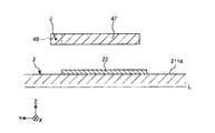
図1および図2に示す振動子1は、Y軸まわりの角速度ωyを検出することのできるジャイロセンサー(角速度センサー)である。このような振動子1は、基板2と、蓋体3と、機能素子4と、を有する。なお、説明の便宜上、図1では、基板2および蓋体3の図示を省略している。
The
基板2は、ベース基板21と、ベース基板21に支持された固定検出電極22と、を有する。ベース基板21は、上面に開放する凹部211と、凹部211内に設けられたポスト(突起部)212と、を有し、上面とポスト212とで機能素子4を支持している。また、固定検出電極22は、凹部211の底面211aに2つ設けられている。一方、蓋体3は、下面に開放する凹部31を有する。これらベース基板21と蓋体3とが、凹部211と凹部31とで内部空間Sを形成するように接合されている。そして、内部空間Sに機能素子4が収容されている。なお、内部空間Sは、減圧状態であることが好ましい。これにより、粘性抵抗が減り、機能素子4を効率的に振動させることができる。
The
本実施形態では、ベース基板21がガラス基板から形成されており、蓋体3がシリコン基板から形成されている。そのため、ベース基板21と蓋体3とを陽極接合によって接合することができる。ただし、ベース基板21および蓋体3の材料としては、これに限定されないし、ベース基板21と蓋体3との接合方法も、これに限定されない。
In the present embodiment, the
機能素子4は、前述したように、内部空間Sに配置されており、ベース基板21の上面とポスト212とに接合されている。このような機能素子4は、2つの構造体40(40a、40b)を有する。2つの構造体40a、40bは、X軸方向に並んで設けられており、Y軸に沿う仮想直線αに対して対称となっている。
As described above, the
構造体40は、質量部(振動部)41と、駆動バネ部42と、固定部43と、可動駆動電極44と、固定駆動電極45、46と、検出用フラップ板(可動部)47と、梁部48と、を有する。このような構造体40は、リン、ボロン等の不純物がドープされた導電性のシリコン基板をエッチング等によってパターニングすることで一体的に形成されている。
The
質量部41は、矩形の枠体であり、構造体40の中央部に配置されている。そして、質量部41の4隅にそれぞれ駆動バネ部42の一端部が接続されている。また、駆動バネ部42の他端部は、固定部43に接続されており、固定部43は、ベース基板21の上面またはポスト212に接合(固定)されている。これにより、質量部41および駆動バネ部42が基板2から浮いた状態で支持された状態となる。そして、駆動バネ部42をX軸方向に伸縮(弾性変形)させることで、質量部41を固定部43に対してX軸方向に振動させることができる。なお、固定部43とポスト212との接合方法としては、特に限定されないが、例えば、陽極接合を用いることができる。
The
可動駆動電極44は、質量部41に設けられており、本実施形態では、質量部41の+Y軸側に2つ、−Y軸側に2つ、計4つ設けられている。これら可動駆動電極44は、質量部41からY軸方向に延出する幹部と、この幹部からX軸方向に延出する複数の枝部と、を備えた櫛歯形状となっている。一方、固定駆動電極45、46は、ベース基板21に接合(固定)されている。固定駆動電極45、46は、可動駆動電極44と対向して設けられ、固定駆動電極45、46の間に可動駆動電極44が配置されている。また、固定駆動電極45、46は、Y軸方向に延在する幹部と、この幹部からX軸方向に延在する枝部と、を備えた櫛歯形状となっている。
The
そのため、可動駆動電極44と固定駆動電極45、46との間に駆動電圧を印加すると、可動駆動電極44と固定駆動電極45、46との間に静電力が発生し、これにより、駆動バネ部42をX軸方向に伸縮させつつ、質量部41をX軸方向に振動(駆動)させることができる。なお、構造体40aと構造体40bとでは、固定駆動電極45と固定駆動電極46の配置が逆である。すなわち、構造体40aでは、可動駆動電極44の−X軸側に固定駆動電極45が位置し、+X軸側に固定駆動電極46が位置しているのに対して、構造体40bでは、可動駆動電極44の+X軸側に固定駆動電極45が位置し、−X軸側に固定駆動電極46が位置している。そのため、構造体40aの質量部41と、構造体40bの質量部41は、互いに接近、離間するようにX軸方向に逆位相で振動する。これにより、2つの質量部41の振動をキャンセルことができ、振動漏れを低減することができる。
Therefore, when a drive voltage is applied between the
なお、本実施形態では、上述したように、静電力によって質量部41を振動させる形態(静電駆動方式)について説明したが、質量部41を振動させる方法は、特に限定されず、圧電駆動方式や、磁場のローレンツ力を利用した電磁駆動方式等を適用することもできる。
In the present embodiment, as described above, the mode in which the
検出用フラップ板47は、質量部41の内側に配置されている。また、検出用フラップ板47は、矩形の板状をなし、Y軸方向の一端部において梁部48を介して質量部41に支持されている。このような検出用フラップ板47は、質量部41をX軸方向に振動させた状態の振動子1にY軸まわりの角速度ωyが加わることで、コリオリの力によって、梁部48を捩り変形(弾性変形)させつつ、梁部48で形成された回動軸Jまわりに回動(変位)する。これにより、検出用フラップ板47をスムーズにZ軸方向に変位させることができる。
The
ベース基板21の検出用フラップ板47と対向する領域(Z軸方向から見た平面視で重なる領域)には固定検出電極22が設けられており、固定検出電極22と検出用フラップ板47との間に静電容量Cが形成されている。前述したように、角速度ωyによって検出用フラップ板47が回動軸Jまわりに変位(傾倒)すると、静電容量Cの大きさが変化するため、この静電容量Cの変化に基づいて角速度ωyを検出することができる。なお、固定検出電極22の構成材料としては、導電性を有していれば特に限定されず、例えば、アルミニウム、金、白金、ITO(Indium Tin Oxide)等を用いることができる。
The fixed
以上、振動子1の形状について説明した。次に、振動子1の動作について説明する。可動駆動電極44と固定駆動電極45、46との間に駆動電圧を印加し、構造体40aの質量部41と構造体40bの質量部41とを逆位相でかつ所定の周波数でX軸方向に振動させる。この状態において、振動子1にY軸まわりの角速度ωyが加わると、コリオリ力が働き、構造体40aの検出用フラップ板47と、構造体40bの検出用フラップ板47とが、回動軸Jまわりに(Z軸方向に)逆位相で変位する。検出用フラップ板47が変位することで、検出用フラップ板47と固定検出電極22とのギャップが変化し、それに伴って静電容量Cが変化するため、この静電容量Cの変化量を検出することで、角速度ωyを求めることができる。
The shape of the
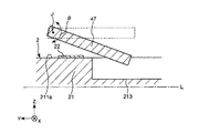
次に、振動子1の特徴の1つである、検出用フラップ板47の可動域について詳細に説明する。前述したように、検出用フラップ板47は、質量部41を駆動させた状態で角速度ωyが加わることで、Z軸方向に振動するようになっている。振動子1では、検出用フラップ板47がZ軸方向に振動する際に、固定検出電極22との間に作用する静電力(電気的な引力)によって固定検出電極22に貼り付いてしまうことを低減する構成となっている。
Next, the movable range of the
まず、静電力による検出用フラップ板47の固定検出電極22への貼り付きについて説明する。まず、図3に示すように、振動子1の側面視(X軸方向から見た平面視)で、固定検出電極22との間に作用する静電力と、梁部48の復元力(自然状態へ戻ろうとする力。ばね定数)と、が等しくなる境界をプルイン臨界(可動臨界)Lとする。すなわち、検出用フラップ板47がプルイン臨界Lよりも上側(+Z軸側)に位置していれば、梁部48の復元力の方が、検出用フラップ板47と固定検出電極22との間に作用する静電力よりも大きく、検出用フラップ板47の少なくとも一部がプルイン臨界Lよりも下側(−Z軸側)に位置していれば、梁部48の復元力の方が、検出用フラップ板47と固定検出電極22との間に作用する静電力よりも小さいことを意味する。
First, sticking of the
そのため、例えば、過度な角速度ωyや検出用フラップ板47をZ軸方向へ変位させるその他の外力が加わり、検出用フラップ板47がプルイン臨界Lよりも下側まで変位してしまうと、梁部48の復元力が静電力に対抗しきれず、検出用フラップ板47が固定検出電極22に引き付けられ、図4に示すように、基板2に貼り付いてしまうおそれがある。
Therefore, for example, if an excessive angular velocity ωy or other external force for displacing the
そこで、振動子1では、図5に示すように、プルイン臨界Lが基板2の検出用フラップ板47と対向する面(本実施形態では、固定検出電極22の上面)よりも下側(検出用フラップ板47と反対側)に位置するように、梁部48のばね定数や、固定検出電極22の面積等を設計している。このような設計とすると、図6に示すように、検出用フラップ板47がプルイン臨界Lを超える前に、検出用フラップ板47が基板2とぶつかり、それ以上の変位が規制される。言い換えると、検出用フラップ板47が基板2と接触するまで−Z軸方向に変位しても、検出用フラップ板47がプルイン臨界Lよりも下側へ変位することがない。すなわち、プルイン臨界Lを超える前に検出用フラップ板47が基板2に接触する。そのため、常に、検出用フラップ板47をプルイン臨界Lよりも上側の領域内で振動させることができる。したがって、振動子1によれば、上述したような、検出用フラップ板47の基板2への貼り付きを低減することができる。
Therefore, in the
なお、振動子1のように、プルイン臨界Lを固定検出電極22の上面よりも下側に位置させるために、例えば、梁部48のバネ定数を次のように設定することができる。すなわち、梁部48のバネ定数をkrとし、内部空間Sの誘電率をεとし、固定検出電極22の面積をSeとし、検出用フラップ板47と固定検出電極22との間に印加する電圧をVとし、初期状態での検出用フラップ板47と固定検出電極22との離間距離をd、検出用フラップ板47との長さ(Y軸方向の長さ)をlとしたとき、下記式(1)を満足することで、プルイン臨界Lを固定検出電極22の上面よりも下側に位置させることができる。
Kr>ε・Se・V2・(l/d(3/2))/√2…(1)
In order to position the pull-in critical L below the upper surface of the fixed
Kr> ε · Se · V2 · ( l / d (3/2)) / √2 ... (1)
以上、本実施形態の振動子1について説明した。なお、本実施形態の振動子1では、検出用フラップ板47がZ軸方向に過度に変位すると、固定検出電極22に接触するようになっているため、接触時にショートが発生するおそれがある。そのため、図7に示すように、検出用フラップ板47がZ軸方向に過度に変位すると、固定検出電極22ではなくて凹部211の底面211aと接触するように構成されていてもよい。底面211aは、基板2が必ずしも露出していなくてもよい。例えば、基板2の上面に導電膜や検出用フラップ板47と電気的に接続された導電膜が設けられていてもよい。この場合は、底面211aまたは導電膜より下側にプルイン臨界Lが位置していればよい。
As above, the
なお、図7に示す構成とすることで、検出用フラップ板47と固定検出電極22との対向面積が減る。また、固定検出電極22を梁部48側に寄せて配置しているため、検出用フラップ板47が変位したときに、検出用フラップ板47と固定検出電極22とのギャップの変化量が小さくなる。そのため、検出用フラップ板47と固定検出電極22との間の静電力の変動が小さくなり、検出用フラップ板47の基板2への貼り付きをより効果的に低減することができる。
Note that the configuration shown in FIG. 7 reduces the facing area between the
以上、第1実施形態の振動子1について説明した。なお、本実施形態では、各構造体40が1つの検出用フラップ板47を備えた構成について説明しているが、検出用フラップ板47の数としては、1つに限定されない。例えば、図8および図9に示すように、検出用フラップ板47がY軸方向に並んで2つ設けられていてもよい。この構成では、2つの検出用フラップ板47を自由端同士が背を向けるように配置しているが、例えば、自由端同士が向き合うように配置してもよいし、自由端同士が同じ方向を向くように配置してもよい。
As described above, the
<第2実施形態>
次に、本発明の第2実施形態に係る振動子について説明する。
<Second embodiment>
Next, a vibrator according to a second embodiment of the present invention will be described.
図10は、本発明の第2実施形態に係る振動子が備える検出用フラップ板を示す平面図である。図11は、固定検出電極の変形例を示す平面図である。図12および図13は、それぞれ、検出用フラップ板の変形例を示す平面図である。 FIG. 10 is a plan view illustrating a detection flap plate included in the vibrator according to the second embodiment of the present invention. FIG. 11 is a plan view showing a modification of the fixed detection electrode. 12 and 13 are plan views each showing a modification of the detection flap plate.
本実施形態に係る振動子では、主に、機能素子の構成(検出用フラップ板の形状)が異なること以外は、前述した第1実施形態にかかる振動子と同様である。 The vibrator according to the present embodiment is the same as the vibrator according to the above-described first embodiment, except that the configuration of the functional element (the shape of the detection flap plate) is different.
なお、以下の説明では、第2実施形態の振動子に関し、前述した実施形態との相違点を中心に説明し、同様の事項に関してはその説明を省略する。また、図10ないし図12では前述した実施形態と同様の構成について、同一符号を付している。 In the following description, the vibrator according to the second embodiment will be described focusing on differences from the above-described embodiment, and description of the same items will be omitted. 10 to 12, the same components as those in the above-described embodiment are denoted by the same reference numerals.
図10に示す機能素子4では、検出用フラップ板47が、その先端部から先端側へ突出する突出部471を有する。本実施形態では、略矩形の突出部471が互いに離間して複数設けられている。このような突出部471を設けることで、検出用フラップ板47の先端に凹凸が形成されるため、検出用フラップ板47が基板2に接触した際の基板2との接触面積を、例えば、前述した第1実施形態と比較して小さくすることができる。したがって、前述した静電力の影響を小さくすることができると共に、静電力以外の要因に起因した検出用フラップ板47の基板2への貼り付きを低減することができる。なお、静電力以外の要因としては、例えば、検出用フラップ板47と基板2との接触による接触帯電や、検出用フラップ板47と基板2との接触摩擦(微小な凹凸同士の引っ掛かり)等による貼り付きが挙げられる。
In the
このような第2実施形態によっても、前述した第1実施形態と同様の効果を発揮することができる。 According to the second embodiment, the same effects as those of the first embodiment can be obtained.
なお、突出部471と固定検出電極22との接触を防止するために、図11に示すように、固定検出電極22の突出部471と対向する部分を除去してもよい。また、突出部471の形状としては、検出用フラップ板47と基板2との接触面積を小さくすることができれば、特に限定されない。例えば、突出部471は、図12に示すような三角形状や、図13に示すような半円形状等、先端へ向けて幅が漸減するテーパー状をなしていてもよい。また、突出部471の数としては、特に限定されず、1つであってもよい。
Note that, in order to prevent the contact between the
<第3実施形態>
次に、本発明の第3実施形態に係る振動子について説明する。
<Third embodiment>
Next, a resonator according to a third embodiment of the present invention will be described.
図14は、本発明の第3実施形態に係る振動子の断面図である。図15は、検出用フラップ板が基板に接触した状態を示す断面図である。図16は、基板に設けられた角部を示す平面図である。図17は、図16中のC−C線断面図である。図18および図19は、それぞれ、図16に示す角部の変形例を示す平面図である。 FIG. 14 is a sectional view of a vibrator according to the third embodiment of the present invention. FIG. 15 is a cross-sectional view showing a state in which the detection flap plate is in contact with the substrate. FIG. 16 is a plan view showing a corner provided on the substrate. FIG. 17 is a sectional view taken along line CC in FIG. 18 and 19 are plan views each showing a modified example of the corner shown in FIG.
本実施形態に係る振動子では、主に、基板の構成が異なっていること以外は、前述した第1実施形態にかかる振動子と同様である。 The vibrator according to the present embodiment is the same as the vibrator according to the above-described first embodiment except that the configuration of the substrate is different.
なお、以下の説明では、第3実施形態の振動子に関し、前述した実施形態との相違点を中心に説明し、同様の事項に関してはその説明を省略する。また、図14ないし16では前述した実施形態と同様の構成について、同一符号を付している。 In the following description, the resonator according to the third embodiment will be described focusing on the differences from the above-described embodiment, and the description of the same items will be omitted. In FIGS. 14 to 16, the same components as those in the above-described embodiment are denoted by the same reference numerals.
図14に示す基板2では、凹部211の底面211aの検出用フラップ板47と対向する位置に、下側へ凹む段差部(凹部)213が形成されている。この段差部213は、検出用フラップ板47と基板2との接触を防止するための逃げ部として機能する。このような段差部213を設けることで、段差部213がない場合(例えば前述した第1実施形態)と比較して、検出用フラップ板47の回動角度θを大きくすることができる。そのため、より大きい角速度ωyが検出可能となり、角速度ωyの検出許容範囲を広くすることができる。
In the
このような第3実施形態によっても、前述した第1実施形態と同様の効果を発揮することができる。 According to the third embodiment, the same effects as those of the first embodiment can be exerted.
なお、本実施形態では、検出用フラップ板47は、図15に示すように、底面211aと段差部213との接続部に形成された角部214に接触し得る。そのため、角部214は、検出用フラップ板47のそれ以上の変位(−Z軸側への変位)を規制するストッパーとして機能するとも言える。このように、角部214がストッパーとして機能することから、プルイン臨界Lは、角部214よりも下方(段差部213の底面側)に位置することが好ましく、段差部213の底面側よりも下方に位置することがより好ましい。これにより、検出用フラップ板47の基板2への貼り付きをより効果的に低減することができる。
In the present embodiment, as shown in FIG. 15, the
このような角部214(検出用フラップ板47と接触する位置)には、図16および図17に示すような凹凸を形成してもよい。図16および図17の構成では、角部214から段差部213内へ突出する矩形状の突出部215が互いに離間して複数設けられていることで凹凸が形成されている。このような構成とすることで、前述した第2実施形態と同様に、基板2と検出用フラップ板47との接触面積を小さくすることができるため、静電力の影響を小さくすることができると共に、静電力以外の要因に起因した検出用フラップ板47の基板2への貼り付きを低減することができる。
Such corner portions 214 (positions that come into contact with the detection flap plate 47) may be formed with irregularities as shown in FIGS. In the configuration of FIG. 16 and FIG. 17, unevenness is formed by providing a plurality of
なお、突出部215の形状としては、検出用フラップ板47と基板2との接触面積を小さくすることができれば、特に限定されない。例えば、突出部215は、図18に示すような三角形状や、図19に示すような半円形状等、先端へ向けて幅が漸減するテーパー状をなしていてもよい。また、突出部215の数としては、特に限定されず、1つであってもよい。
The shape of the
次に、本発明の振動子を備える電子機器について説明する。
図20は、本発明の電子機器を適用したモバイル型(またはノート型)のパーソナルコンピューターの構成を示す斜視図である。
Next, an electronic device including the vibrator of the invention will be described.
FIG. 20 is a perspective view showing a configuration of a mobile (or notebook) personal computer to which the electronic device of the present invention is applied.
この図において、パーソナルコンピューター1100は、キーボード1102を備えた本体部1104と、表示部1108を備えた表示ユニット1106とにより構成され、表示ユニット1106は、本体部1104に対しヒンジ構造部を介して回動可能に支持されている。このようなパーソナルコンピューター1100には、ジャイロセンサーとして機能する振動子1が内蔵されている。
In this figure, a
図21は、本発明の電子機器を適用した携帯電話機(PHSも含む)の構成を示す斜視図である。 FIG. 21 is a perspective view illustrating a configuration of a mobile phone (including a PHS) to which the electronic device of the present invention is applied.
この図において、携帯電話機1200は、アンテナ(図示せず)、複数の操作ボタン1202、受話口1204および送話口1206を備え、操作ボタン1202と受話口1204との間には、表示部1208が配置されている。このような携帯電話機1200には、ジャイロセンサーとして機能する振動子1が内蔵されている。
In this drawing, a
図22は、本発明の電子機器を適用したデジタルスチールカメラの構成を示す斜視図である。 FIG. 22 is a perspective view illustrating a configuration of a digital still camera to which the electronic apparatus according to the invention is applied.
デジタルスチールカメラ1300におけるケース(ボディー)1302の背面には表示部1310が設けられ、CCDによる撮像信号に基づいて表示を行う構成になっており、表示部1310は、被写体を電子画像として表示するファインダーとして機能する。また、ケース1302の正面側(図中裏面側)には、光学レンズ(撮像光学系)やCCDなどを含む受光ユニット1304が設けられている。そして、撮影者が表示部1310に表示された被写体像を確認し、シャッターボタン1306を押すと、その時点におけるCCDの撮像信号が、メモリー1308に転送・格納される。このようなデジタルスチールカメラ1300には、例えば、ジャイロセンサーとして手振れ補正に用いられる振動子1が内蔵されている。
このような電子機器は、振動子1を備えているので、優れた信頼性を有している。
A
Since such an electronic device includes the
なお、本発明の電子機器は、図20のパーソナルコンピューター、図21の携帯電話機、図22のデジタルスチールカメラの他にも、例えば、スマートフォン、タブレット端末、時計、インクジェット式吐出装置(例えばインクジェットプリンタ)、ラップトップ型パーソナルコンピューター、テレビ、ビデオカメラ、ビデオテープレコーダ、カーナビゲーション装置、ページャ、電子手帳(通信機能付も含む)、電子辞書、電卓、電子ゲーム機器、ワードプロセッサ、ワークステーション、テレビ電話、防犯用テレビモニタ、電子双眼鏡、POS端末、医療機器(例えば電子体温計、血圧計、血糖計、心電図計測装置、超音波診断装置、電子内視鏡)、魚群探知機、各種測定機器、計器類(例えば、車両、航空機、船舶の計器類)、フライトシュミレータ等に適用することができる。 In addition to the personal computer shown in FIG. 20, the mobile phone shown in FIG. 21, and the digital still camera shown in FIG. 22, the electronic apparatus of the present invention includes, for example, a smartphone, a tablet terminal, a clock, and an ink jet type ejection device (eg, an ink jet printer). , Laptop personal computer, television, video camera, video tape recorder, car navigation system, pager, electronic organizer (including communication function), electronic dictionary, calculator, electronic game machine, word processor, workstation, videophone, crime prevention TV monitor, electronic binoculars, POS terminal, medical equipment (for example, electronic thermometer, sphygmomanometer, blood glucose meter, electrocardiogram measuring device, ultrasonic diagnostic device, electronic endoscope), fish finder, various measuring devices, instruments (for example, , Instruments for vehicles, aircraft, ships), fly It can be applied to a simulator or the like.
次に、本発明の移動体について説明する。
図23は、本発明の移動体を適用した自動車を示す斜視図である。
Next, the moving object of the present invention will be described.
FIG. 23 is a perspective view showing an automobile to which the moving body of the present invention is applied.
図23に示すように、自動車1500には振動子1が内蔵されており、例えば、振動子1によって車体1501の姿勢を検出することができる。振動子1の検出信号は、車体姿勢制御装置1502に供給され、車体姿勢制御装置1502は、その信号に基づいて車体1501の姿勢を検出し、検出結果に応じてサスペンションの硬軟を制御したり、個々の車輪1503のブレーキを制御したりすることができる。その他、このような姿勢制御は、二足歩行ロボットやラジコンヘリコプター(ドローンを含む)で利用することができる。以上のように、各種移動体の姿勢制御の実現にあたって、振動子1が組み込まれる。
As shown in FIG. 23, the
以上、本発明の振動子、電子機器および移動体を図示の実施形態に基づいて説明したが、本発明はこれに限定されるものではなく、各部の構成は、同様の機能を有する任意の構成のものに置換することができる。また、本発明に、他の任意の構成物が付加されていてもよい。 As described above, the vibrator, the electronic device, and the moving body of the present invention have been described based on the illustrated embodiment. However, the present invention is not limited to this, and the configuration of each unit may be any configuration having the same function. Can be replaced by Further, other arbitrary components may be added to the present invention.
また、前述した実施形態では、検出用フラップ板が回動軸まわりに回動する構成について説明したが、検出用フラップ板としては、Z軸方向に変位することができれば、どのように変位してもよい。例えば、検出用フラップ板は、回動軸まわりにシーソー揺動してもよいし、姿勢を保ったままZ軸方向に変位していてもよい。すなわち、シーソー揺動型の振動子であってもよいし、平行平板型の振動子であってもよい。 In the above-described embodiment, the configuration in which the detection flap plate rotates around the rotation axis has been described. However, as long as the detection flap plate can be displaced in the Z-axis direction, Is also good. For example, the detection flap plate may swing the seesaw around the rotation axis, or may be displaced in the Z-axis direction while maintaining the posture. That is, it may be a seesaw swing type vibrator or a parallel plate type vibrator.
また、振動子としては、角速度を検出するジャイロセンサーに限定されず、例えば、加速度センサー、気圧センサー等の角速度以外の物理量を検知する物理量センサーであってもよい。また、物理量センサー以外にも、例えば、発振器等に用いられる振動子であってもよい。 Further, the vibrator is not limited to a gyro sensor that detects an angular velocity, but may be a physical quantity sensor that detects a physical quantity other than the angular velocity, such as an acceleration sensor or a barometric pressure sensor. Further, other than the physical quantity sensor, for example, a vibrator used for an oscillator or the like may be used.
1…振動子、2…基板、21…ベース基板、211…凹部、211a…底面、212…ポスト、213…段差部、214…角部、215…突出部、22…固定検出電極、3…蓋体、31…凹部、4…機能素子、40…構造体、40a、40b…構造体、41…質量部、42…駆動バネ部、43…固定部、44…可動駆動電極、45、46…固定駆動電極、47…検出用フラップ板、471…突出部、48…梁部、1100…パーソナルコンピューター、1102…キーボード、1104…本体部、1106…表示ユニット、1108…表示部、1200…携帯電話機、1202…操作ボタン、1204…受話口、1206…送話口、1208…表示部、1300…デジタルスチールカメラ、1302…ケース、1304…受光ユニット、1306…シャッターボタン、1308…メモリー、1310…表示部、1500…自動車、1501…車体、1502…車体姿勢制御装置、1503…車輪、C…静電容量、J…回動軸、L…プルイン臨界、S…内部空間、α…仮想直線、θ…回動角度、ωy…角速度
DESCRIPTION OF
Claims (11)
前記X軸および前記Y軸を含む平面に沿っている底面を含む第1の凹部が設けられているベース基板と、
前記第1の凹部に対向している第2の凹部が設けられ、前記第1の凹部と前記第2の凹部との間に内部空間が形成されるように、前記ベース基板に接合されている蓋体と、
前記第1の凹部の前記底面に設けられている固定検出電極と、
前記固定検出電極と前記Z軸方向に離間して対向するように配置されている可動部、及び前記可動部に連結され、前記X軸に沿って配置されている梁部を含み、前記内部空間に配置されている構造体と、
を含み、
前記可動部は、前記梁部を回動軸として揺動可能であり、
前記梁部のバネ定数をkr、
前記内部空間の誘電率をε、
前記Z軸方向からの平面視で、前記固定検出電極の面積をSe、
前記可動部と前記固定検出電極との間に印加する電圧をV、
初期状態での前記可動部と前記固定検出電極との離間距離をd、
前記可動部の前記Y軸に沿った長さをlとしたとき、
Kr>ε・Se・V 2 ・(l/d (3/2) )/√2
を満足することを特徴とする物理量センサー。 When three axes orthogonal to each other are defined as an X axis, a Y axis, and a Z axis,
A base substrate provided with a first concave portion including a bottom surface extending along a plane including the X axis and the Y axis ;
A second concave portion facing the first concave portion is provided, and is joined to the base substrate so that an internal space is formed between the first concave portion and the second concave portion. A lid,
A fixed detection electrode provided on the bottom surface of the first recess,
A movable portion arranged to face the fixed detection electrode at a distance in the Z-axis direction, and a beam portion connected to the movable portion and arranged along the X-axis; A structure located at
Including
The movable portion is swingable around the beam portion as a rotation axis,
The spring constant of the beam part is kr,
The dielectric constant of the internal space is ε,
In a plan view from the Z-axis direction, the area of the fixed detection electrode is Se,
The voltage applied between the movable part and the fixed detection electrode is V,
The distance between the movable portion and the fixed detection electrode in the initial state is d,
When the length of the movable portion along the Y axis is l,
Kr> ε · Se · V 2 · (l / d (3/2) ) / √2
Physical quantity sensor characterized by satisfying the following .
前記固定検出電極と前記可動部との間に生じる静電力と、前記梁部の復元力と、が等しくなる位置を可動臨界としたとき、
前記X軸方向からの側面視で、
前記可動部は、前記可動臨界を超える前に、前記ベース基板又は前記固定検出電極と接触することを特徴とする物理量センサー。 In claim 1,
When the electrostatic force generated between the fixed detection electrode and the movable unit, and the restoring force of the beam portion, a movable critical the equal position,
In a side view from the X-axis direction,
The movable part, before exceeding the movable critical, the physical quantity sensor, characterized by contacting the base substrate or the fixed sensing electrode.
前記可動臨界は、前記ベース基板の前記可動部と対向する面に対して、前記可動部の側とは反対側に位置することを特徴とする物理量センサー。 In claim 2,
The movable criticality, the physical quantity sensor, characterized in that with respect to the movable portion and the opposing surfaces of the base substrate, the side of the movable portion on the opposite side.
前記構造体は、枠状の質量部を含み、
前記Z軸方向からの平面視で、前記可動部は、前記質量部の内側に配置され、
前記可動部は、前記梁部を介して、前記質量部に支持されていることを特徴とする物理量センサー。 In any one of claims 1 to 3,
The structure includes a frame-shaped mass part,
In a plan view from the Z-axis direction, the movable unit is disposed inside the mass unit,
The physical quantity sensor, wherein the movable part is supported by the mass part via the beam part .
前記可動部は、前記Y軸に沿って並んでいる第1の可動部と第2の可動部とから構成されていることを特徴とする物理量センサー。 In claim 4,
The physical quantity sensor, wherein the movable part includes a first movable part and a second movable part arranged along the Y axis .
前記構造体は、駆動電極と駆動バネを含み、
前記質量部は、矩形状であり、
前記駆動バネの一端部は、前記質量部に接続され、
前記駆動バネの他端部は、前記ベース基板に接続されていることを特徴とする物理量センサー。 In claim 4 or 5,
The structure includes a driving electrode and a driving spring,
The mass section is rectangular,
One end of the drive spring is connected to the mass,
The other end of the driving spring is connected to the base substrate .
前記可動部は、前記質量部に向かって突出している突出部を含むことを特徴とする物理量センサー。 In any one of claims 4 to 6,
The physical quantity sensor , wherein the movable part includes a protruding part protruding toward the mass part .
前記ベース基板は、
前記Z軸方向からの平面視で、前記可動部の先端部と対向する位置に配置され、
且つ、前記可動部の側とは反対側へ凹む段差部が設けられていることを特徴とする物理量センサー。 In any one of claims 1 to 7,
The base substrate,
In a plan view from the Z-axis direction, the movable portion is disposed at a position facing the distal end portion,
And, the physical quantity sensor, wherein a stepped portion which is recessed to the opposite side is provided to the side of the movable portion.
前記ベース基板の前記可動部と接触し得る箇所には、凹凸が形成されていることを特徴とする物理量センサー。 In any one of claims 1 to 8,
A physical quantity sensor , wherein irregularities are formed in a portion of the base substrate that can contact the movable portion.
Priority Applications (3)
| Application Number | Priority Date | Filing Date | Title |
|---|---|---|---|
| JP2015182057A JP6623634B2 (en) | 2015-09-15 | 2015-09-15 | Physical quantity sensors, electronic devices and moving objects |
| US15/260,793 US10215566B2 (en) | 2015-09-15 | 2016-09-09 | Oscillator, electronic device, and moving object |
| CN201610821869.1A CN107036590A (en) | 2015-09-15 | 2016-09-13 | Oscillator, electronic equipment and moving body |
Applications Claiming Priority (1)
| Application Number | Priority Date | Filing Date | Title |
|---|---|---|---|
| JP2015182057A JP6623634B2 (en) | 2015-09-15 | 2015-09-15 | Physical quantity sensors, electronic devices and moving objects |
Publications (3)
| Publication Number | Publication Date |
|---|---|
| JP2017058197A JP2017058197A (en) | 2017-03-23 |
| JP2017058197A5 JP2017058197A5 (en) | 2018-09-27 |
| JP6623634B2 true JP6623634B2 (en) | 2019-12-25 |
Family
ID=58257249
Family Applications (1)
| Application Number | Title | Priority Date | Filing Date |
|---|---|---|---|
| JP2015182057A Active JP6623634B2 (en) | 2015-09-15 | 2015-09-15 | Physical quantity sensors, electronic devices and moving objects |
Country Status (3)
| Country | Link |
|---|---|
| US (1) | US10215566B2 (en) |
| JP (1) | JP6623634B2 (en) |
| CN (1) | CN107036590A (en) |
Families Citing this family (5)
| Publication number | Priority date | Publication date | Assignee | Title |
|---|---|---|---|---|
| JP6711305B2 (en) | 2017-03-23 | 2020-06-17 | 株式会社デンソー | Rotating electric machine control device |
| JP2019060675A (en) * | 2017-09-26 | 2019-04-18 | セイコーエプソン株式会社 | Physical quantity sensor, physical quantity sensor device, electronic apparatus, and moving body |
| WO2019114239A1 (en) * | 2017-12-13 | 2019-06-20 | 清华大学 | Terahertz detection method and system for highly hazardous chemical in atmosphere |
| JP7192437B2 (en) * | 2018-11-28 | 2022-12-20 | セイコーエプソン株式会社 | Inertial sensors, electronics and vehicles |
| JP2020101484A (en) * | 2018-12-25 | 2020-07-02 | セイコーエプソン株式会社 | Inertia sensor, electronic apparatus and moving body |
Family Cites Families (14)
| Publication number | Priority date | Publication date | Assignee | Title |
|---|---|---|---|---|
| JP3597806B2 (en) | 2001-09-25 | 2004-12-08 | 東京エレクトロン株式会社 | Microstructure having movable structure and method of manufacturing the same |
| JP2004361115A (en) | 2003-06-02 | 2004-12-24 | Denso Corp | Semiconductor dynamic amount sensor |
| JP2005283393A (en) | 2004-03-30 | 2005-10-13 | Fujitsu Media Device Kk | Inertia sensor |
| WO2006034706A1 (en) | 2004-09-27 | 2006-04-06 | Conti Temic Microelectronic Gmbh | Rotation speed sensor |
| ATE425544T1 (en) | 2005-10-14 | 2009-03-15 | Nxp Bv | TUNABLE MEMS ARRANGEMENT |
| JP4998401B2 (en) | 2008-07-29 | 2012-08-15 | 大日本印刷株式会社 | Acceleration sensor and manufacturing method thereof |
| JP5493691B2 (en) | 2009-10-21 | 2014-05-14 | 大日本印刷株式会社 | Method for forming stopper, method for manufacturing mechanical quantity sensor, and mechanical quantity sensor |
| US8555720B2 (en) * | 2011-02-24 | 2013-10-15 | Freescale Semiconductor, Inc. | MEMS device with enhanced resistance to stiction |
| JP5811634B2 (en) * | 2011-06-30 | 2015-11-11 | セイコーエプソン株式会社 | Physical quantity sensor, electronic equipment |
| JP5790296B2 (en) * | 2011-08-17 | 2015-10-07 | セイコーエプソン株式会社 | Physical quantity sensor and electronic equipment |
| JP5979344B2 (en) * | 2012-01-30 | 2016-08-24 | セイコーエプソン株式会社 | Physical quantity sensor and electronic equipment |
| JP2013160554A (en) * | 2012-02-02 | 2013-08-19 | Seiko Epson Corp | Physical quantity sensor, manufacturing method thereof, and electronic apparatus |
| JP6098780B2 (en) * | 2012-04-19 | 2017-03-22 | セイコーエプソン株式会社 | Gyro sensor and electronics |
| US9476712B2 (en) * | 2013-07-31 | 2016-10-25 | Honeywell International Inc. | MEMS device mechanism enhancement for robust operation through severe shock and acceleration |
-
2015
- 2015-09-15 JP JP2015182057A patent/JP6623634B2/en active Active
-
2016
- 2016-09-09 US US15/260,793 patent/US10215566B2/en active Active
- 2016-09-13 CN CN201610821869.1A patent/CN107036590A/en active Pending
Also Published As
| Publication number | Publication date |
|---|---|
| US10215566B2 (en) | 2019-02-26 |
| CN107036590A (en) | 2017-08-11 |
| US20170074654A1 (en) | 2017-03-16 |
| JP2017058197A (en) | 2017-03-23 |
Similar Documents
| Publication | Publication Date | Title |
|---|---|---|
| US9383383B2 (en) | Physical quantity sensor, manufacturing method thereof, and electronic apparatus | |
| JP6098780B2 (en) | Gyro sensor and electronics | |
| JP6623634B2 (en) | Physical quantity sensors, electronic devices and moving objects | |
| JP6205921B2 (en) | Physical quantity sensors, electronic devices, and moving objects | |
| JP6146566B2 (en) | Physical quantity sensors, electronic devices, and moving objects | |
| JP6338813B2 (en) | Gyro sensor and electronic device using the same | |
| JP6380737B2 (en) | Electronic devices, electronic devices, and moving objects | |
| US9879999B2 (en) | Gyro sensor and electronic apparatus | |
| JP6398348B2 (en) | Functional element, method for manufacturing functional element, electronic device, and moving body | |
| JP6344552B2 (en) | Functional element, electronic device, and moving object | |
| JP6269992B2 (en) | Gyro sensor and electronics | |
| US9243908B2 (en) | Gyro sensor and electronic apparatus | |
| JP5958688B2 (en) | Gyro sensor and electronics | |
| JP2016176835A (en) | Inertia sensor, electronic apparatus, and mobile body | |
| JP6597099B2 (en) | Physical quantity sensor, electronic device and mobile object | |
| JP6922325B2 (en) | Physical quantity sensors, physical quantity sensor devices, electronic devices and mobiles | |
| JP6447049B2 (en) | Physical quantity sensor, electronic device and mobile object | |
| JP2018021920A (en) | Physical amount sensor, electronic apparatus, and moving body | |
| JP2018173288A (en) | Vibration device, method for manufacturing vibration device, vibration device module, electronic apparatus, and mobile body | |
| JP2016176834A (en) | Gyro sensor, electronic apparatus, and mobile body | |
| JP2020016557A (en) | Physical quantity sensor, electronic apparatus, and movable body | |
| JP2018155501A (en) | Physical quantity sensor, physical quantity sensor device, electronic device, and mobile body | |
| JP2017219459A (en) | Physical-quantity sensor, electronic apparatus, and mobile body | |
| JP2016176825A (en) | Physical quantity sensor, method for manufacturing the same, electronic apparatus, and movable body | |
| JP2013234913A (en) | Gyro sensor and electronic apparatus |
Legal Events
| Date | Code | Title | Description |
|---|---|---|---|
| A521 | Written amendment |
Free format text: JAPANESE INTERMEDIATE CODE: A523 Effective date: 20180814 |
|
| A621 | Written request for application examination |
Free format text: JAPANESE INTERMEDIATE CODE: A621 Effective date: 20180814 |
|
| A977 | Report on retrieval |
Free format text: JAPANESE INTERMEDIATE CODE: A971007 Effective date: 20190614 |
|
| A131 | Notification of reasons for refusal |
Free format text: JAPANESE INTERMEDIATE CODE: A131 Effective date: 20190618 |
|
| A521 | Written amendment |
Free format text: JAPANESE INTERMEDIATE CODE: A523 Effective date: 20190815 |
|
| TRDD | Decision of grant or rejection written | ||
| A01 | Written decision to grant a patent or to grant a registration (utility model) |
Free format text: JAPANESE INTERMEDIATE CODE: A01 Effective date: 20191029 |
|
| A61 | First payment of annual fees (during grant procedure) |
Free format text: JAPANESE INTERMEDIATE CODE: A61 Effective date: 20191111 |
|
| R150 | Certificate of patent or registration of utility model |
Ref document number: 6623634 Country of ref document: JP Free format text: JAPANESE INTERMEDIATE CODE: R150 |