JP6623156B2 - Illumination system for EUV projection lithography - Google Patents
Illumination system for EUV projection lithography Download PDFInfo
- Publication number
- JP6623156B2 JP6623156B2 JP2016533541A JP2016533541A JP6623156B2 JP 6623156 B2 JP6623156 B2 JP 6623156B2 JP 2016533541 A JP2016533541 A JP 2016533541A JP 2016533541 A JP2016533541 A JP 2016533541A JP 6623156 B2 JP6623156 B2 JP 6623156B2
- Authority
- JP
- Japan
- Prior art keywords
- optical unit
- euv
- mirror
- mirrors
- deflection
- Prior art date
- Legal status (The legal status is an assumption and is not a legal conclusion. Google has not performed a legal analysis and makes no representation as to the accuracy of the status listed.)
- Active
Links
- 238000005286 illumination Methods 0.000 title claims description 102
- 238000001459 lithography Methods 0.000 title claims description 13
- 230000003287 optical effect Effects 0.000 claims description 308
- 238000007493 shaping process Methods 0.000 claims description 138
- 230000008878 coupling Effects 0.000 claims description 57
- 238000010168 coupling process Methods 0.000 claims description 57
- 238000005859 coupling reaction Methods 0.000 claims description 57
- 230000005855 radiation Effects 0.000 claims description 35
- 238000009304 pastoral farming Methods 0.000 claims description 19
- 230000000694 effects Effects 0.000 claims description 15
- 238000000034 method Methods 0.000 claims description 13
- 230000005469 synchrotron radiation Effects 0.000 claims description 11
- 238000003384 imaging method Methods 0.000 claims description 6
- 238000001900 extreme ultraviolet lithography Methods 0.000 claims description 3
- 239000002086 nanomaterial Substances 0.000 claims description 3
- 238000013461 design Methods 0.000 description 17
- 230000006870 function Effects 0.000 description 15
- 238000009826 distribution Methods 0.000 description 14
- 210000001747 pupil Anatomy 0.000 description 11
- 238000000265 homogenisation Methods 0.000 description 8
- 230000004048 modification Effects 0.000 description 8
- 238000012986 modification Methods 0.000 description 8
- 230000007704 transition Effects 0.000 description 7
- 230000006978 adaptation Effects 0.000 description 6
- 230000002093 peripheral effect Effects 0.000 description 6
- 230000005540 biological transmission Effects 0.000 description 5
- 238000006073 displacement reaction Methods 0.000 description 5
- 238000010894 electron beam technology Methods 0.000 description 5
- 238000011144 upstream manufacturing Methods 0.000 description 5
- 239000000463 material Substances 0.000 description 4
- 238000000926 separation method Methods 0.000 description 4
- 230000000712 assembly Effects 0.000 description 3
- 238000000429 assembly Methods 0.000 description 3
- 238000010586 diagram Methods 0.000 description 3
- 239000003574 free electron Substances 0.000 description 3
- 239000004065 semiconductor Substances 0.000 description 3
- 230000003044 adaptive effect Effects 0.000 description 2
- 230000008901 benefit Effects 0.000 description 2
- 230000008859 change Effects 0.000 description 2
- 238000009434 installation Methods 0.000 description 2
- 230000010287 polarization Effects 0.000 description 2
- 239000011248 coating agent Substances 0.000 description 1
- 238000000576 coating method Methods 0.000 description 1
- 230000001427 coherent effect Effects 0.000 description 1
- 238000001816 cooling Methods 0.000 description 1
- 238000011161 development Methods 0.000 description 1
- 230000005684 electric field Effects 0.000 description 1
- 238000001393 microlithography Methods 0.000 description 1
- 230000007480 spreading Effects 0.000 description 1
- 230000000007 visual effect Effects 0.000 description 1
Images


Classifications
-
- G—PHYSICS
- G03—PHOTOGRAPHY; CINEMATOGRAPHY; ANALOGOUS TECHNIQUES USING WAVES OTHER THAN OPTICAL WAVES; ELECTROGRAPHY; HOLOGRAPHY
- G03F—PHOTOMECHANICAL PRODUCTION OF TEXTURED OR PATTERNED SURFACES, e.g. FOR PRINTING, FOR PROCESSING OF SEMICONDUCTOR DEVICES; MATERIALS THEREFOR; ORIGINALS THEREFOR; APPARATUS SPECIALLY ADAPTED THEREFOR
- G03F7/00—Photomechanical, e.g. photolithographic, production of textured or patterned surfaces, e.g. printing surfaces; Materials therefor, e.g. comprising photoresists; Apparatus specially adapted therefor
- G03F7/20—Exposure; Apparatus therefor
- G03F7/2002—Exposure; Apparatus therefor with visible light or UV light, through an original having an opaque pattern on a transparent support, e.g. film printing, projection printing; by reflection of visible or UV light from an original such as a printed image
- G03F7/2004—Exposure; Apparatus therefor with visible light or UV light, through an original having an opaque pattern on a transparent support, e.g. film printing, projection printing; by reflection of visible or UV light from an original such as a printed image characterised by the use of a particular light source, e.g. fluorescent lamps or deep UV light
- G03F7/2006—Exposure; Apparatus therefor with visible light or UV light, through an original having an opaque pattern on a transparent support, e.g. film printing, projection printing; by reflection of visible or UV light from an original such as a printed image characterised by the use of a particular light source, e.g. fluorescent lamps or deep UV light using coherent light; using polarised light
-
- G—PHYSICS
- G03—PHOTOGRAPHY; CINEMATOGRAPHY; ANALOGOUS TECHNIQUES USING WAVES OTHER THAN OPTICAL WAVES; ELECTROGRAPHY; HOLOGRAPHY
- G03F—PHOTOMECHANICAL PRODUCTION OF TEXTURED OR PATTERNED SURFACES, e.g. FOR PRINTING, FOR PROCESSING OF SEMICONDUCTOR DEVICES; MATERIALS THEREFOR; ORIGINALS THEREFOR; APPARATUS SPECIALLY ADAPTED THEREFOR
- G03F7/00—Photomechanical, e.g. photolithographic, production of textured or patterned surfaces, e.g. printing surfaces; Materials therefor, e.g. comprising photoresists; Apparatus specially adapted therefor
- G03F7/70—Microphotolithographic exposure; Apparatus therefor
- G03F7/70058—Mask illumination systems
- G03F7/7015—Details of optical elements
- G03F7/70183—Zoom systems for adjusting beam diameter
-
- G—PHYSICS
- G03—PHOTOGRAPHY; CINEMATOGRAPHY; ANALOGOUS TECHNIQUES USING WAVES OTHER THAN OPTICAL WAVES; ELECTROGRAPHY; HOLOGRAPHY
- G03F—PHOTOMECHANICAL PRODUCTION OF TEXTURED OR PATTERNED SURFACES, e.g. FOR PRINTING, FOR PROCESSING OF SEMICONDUCTOR DEVICES; MATERIALS THEREFOR; ORIGINALS THEREFOR; APPARATUS SPECIALLY ADAPTED THEREFOR
- G03F7/00—Photomechanical, e.g. photolithographic, production of textured or patterned surfaces, e.g. printing surfaces; Materials therefor, e.g. comprising photoresists; Apparatus specially adapted therefor
- G03F7/70—Microphotolithographic exposure; Apparatus therefor
- G03F7/70008—Production of exposure light, i.e. light sources
- G03F7/70033—Production of exposure light, i.e. light sources by plasma extreme ultraviolet [EUV] sources
-
- G—PHYSICS
- G03—PHOTOGRAPHY; CINEMATOGRAPHY; ANALOGOUS TECHNIQUES USING WAVES OTHER THAN OPTICAL WAVES; ELECTROGRAPHY; HOLOGRAPHY
- G03F—PHOTOMECHANICAL PRODUCTION OF TEXTURED OR PATTERNED SURFACES, e.g. FOR PRINTING, FOR PROCESSING OF SEMICONDUCTOR DEVICES; MATERIALS THEREFOR; ORIGINALS THEREFOR; APPARATUS SPECIALLY ADAPTED THEREFOR
- G03F7/00—Photomechanical, e.g. photolithographic, production of textured or patterned surfaces, e.g. printing surfaces; Materials therefor, e.g. comprising photoresists; Apparatus specially adapted therefor
- G03F7/70—Microphotolithographic exposure; Apparatus therefor
- G03F7/70058—Mask illumination systems
- G03F7/70091—Illumination settings, i.e. intensity distribution in the pupil plane or angular distribution in the field plane; On-axis or off-axis settings, e.g. annular, dipole or quadrupole settings; Partial coherence control, i.e. sigma or numerical aperture [NA]
- G03F7/70116—Off-axis setting using a programmable means, e.g. liquid crystal display [LCD], digital micromirror device [DMD] or pupil facets
-
- G—PHYSICS
- G03—PHOTOGRAPHY; CINEMATOGRAPHY; ANALOGOUS TECHNIQUES USING WAVES OTHER THAN OPTICAL WAVES; ELECTROGRAPHY; HOLOGRAPHY
- G03F—PHOTOMECHANICAL PRODUCTION OF TEXTURED OR PATTERNED SURFACES, e.g. FOR PRINTING, FOR PROCESSING OF SEMICONDUCTOR DEVICES; MATERIALS THEREFOR; ORIGINALS THEREFOR; APPARATUS SPECIALLY ADAPTED THEREFOR
- G03F7/00—Photomechanical, e.g. photolithographic, production of textured or patterned surfaces, e.g. printing surfaces; Materials therefor, e.g. comprising photoresists; Apparatus specially adapted therefor
- G03F7/70—Microphotolithographic exposure; Apparatus therefor
- G03F7/70058—Mask illumination systems
- G03F7/70191—Optical correction elements, filters or phase plates for controlling intensity, wavelength, polarisation, phase or the like
-
- G—PHYSICS
- G03—PHOTOGRAPHY; CINEMATOGRAPHY; ANALOGOUS TECHNIQUES USING WAVES OTHER THAN OPTICAL WAVES; ELECTROGRAPHY; HOLOGRAPHY
- G03F—PHOTOMECHANICAL PRODUCTION OF TEXTURED OR PATTERNED SURFACES, e.g. FOR PRINTING, FOR PROCESSING OF SEMICONDUCTOR DEVICES; MATERIALS THEREFOR; ORIGINALS THEREFOR; APPARATUS SPECIALLY ADAPTED THEREFOR
- G03F7/00—Photomechanical, e.g. photolithographic, production of textured or patterned surfaces, e.g. printing surfaces; Materials therefor, e.g. comprising photoresists; Apparatus specially adapted therefor
- G03F7/70—Microphotolithographic exposure; Apparatus therefor
- G03F7/70058—Mask illumination systems
- G03F7/702—Reflective illumination, i.e. reflective optical elements other than folding mirrors, e.g. extreme ultraviolet [EUV] illumination systems
-
- G—PHYSICS
- G03—PHOTOGRAPHY; CINEMATOGRAPHY; ANALOGOUS TECHNIQUES USING WAVES OTHER THAN OPTICAL WAVES; ELECTROGRAPHY; HOLOGRAPHY
- G03F—PHOTOMECHANICAL PRODUCTION OF TEXTURED OR PATTERNED SURFACES, e.g. FOR PRINTING, FOR PROCESSING OF SEMICONDUCTOR DEVICES; MATERIALS THEREFOR; ORIGINALS THEREFOR; APPARATUS SPECIALLY ADAPTED THEREFOR
- G03F7/00—Photomechanical, e.g. photolithographic, production of textured or patterned surfaces, e.g. printing surfaces; Materials therefor, e.g. comprising photoresists; Apparatus specially adapted therefor
- G03F7/70—Microphotolithographic exposure; Apparatus therefor
- G03F7/708—Construction of apparatus, e.g. environment aspects, hygiene aspects or materials
- G03F7/70991—Connection with other apparatus, e.g. multiple exposure stations, particular arrangement of exposure apparatus and pre-exposure and/or post-exposure apparatus; Shared apparatus, e.g. having shared radiation source, shared mask or workpiece stage, shared base-plate; Utilities, e.g. cable, pipe or wireless arrangements for data, power, fluids or vacuum
Landscapes
- Physics & Mathematics (AREA)
- General Physics & Mathematics (AREA)
- Engineering & Computer Science (AREA)
- Computer Networks & Wireless Communication (AREA)
- Health & Medical Sciences (AREA)
- Environmental & Geological Engineering (AREA)
- Epidemiology (AREA)
- Public Health (AREA)
- Plasma & Fusion (AREA)
- Exposure And Positioning Against Photoresist Photosensitive Materials (AREA)
- Exposure Of Semiconductors, Excluding Electron Or Ion Beam Exposure (AREA)
- Lenses (AREA)
Description
ドイツ特許出願第10 2013 223 935.1号明細書の内容が引用によって本明細書に組み込まれている。 The content of German Patent Application No. 10 2013 223 935.1 is hereby incorporated by reference.
本発明は、EUV投影リソグラフィのための照明系のための偏向光学ユニットに関する。本発明は、EUV投影リソグラフィのための照明系のためのビーム成形光学ユニット及びビーム案内(誘導)光学ユニットに関する。これに加えて、本発明は、EUV投影リソグラフィのための照明系及びEUVリソグラフィのための投影露光装置に関する。最後に、本発明は、構造化構成要素を生成する方法、及び本方法に従って生成された構造化構成要素に関する。 The present invention relates to a deflection optical unit for an illumination system for EUV projection lithography. The present invention relates to a beam shaping optical unit and a beam guiding (guidance) optical unit for an illumination system for EUV projection lithography. In addition, the present invention relates to an illumination system for EUV projection lithography and a projection exposure apparatus for EUV lithography. Finally, the present invention relates to a method for generating a structured component and a structured component generated according to the method.
照明系を含む投影露光装置は、US 2011/0 014 799 A1、WO 2009/121 438 A1、US 2009/0 174 876 A1、US 6,438,199 B1、及びUS 6,658,084 B2から公知である。EUV光源は、DE 103 58 225 B3及びUS 6,859,515 Bから公知である。EUV投影リソグラフィに対する更に別の構成部分は、US 2003/0002022 A1、DE 10 2009 025 655 A1、US 6,700,952、及びUS 2004/0140440 Aから公知である。EUV光源が公知である更に別の参考文献は、WO 2009/121 438 A1に見出される。EUV照明光学ユニットは、US 2003/0043359 A1及びUS 5,896,438から公知である。 Projection exposure apparatus including illumination systems are known from US 2011/0 014 799 A1, WO 2009/121 438 A1, US 2009/0 174 876 A1, US 6,438,199 B1, and US 6,658,084 B2. It is. EUV light sources are known from DE 103 58 225 B3 and US 6,859,515 B. Further components for EUV projection lithography are known from US 2003/0002022 A1, DE 10 2009 025 655 A1, US 6,700,952 and US 2004/0140440 A. Yet another reference in which EUV light sources are known is found in WO 2009/121 438 A1. EUV illumination optical units are known from US 2003/0043359 A1 and US 5,896,438.
本発明の目的は、シンクロトロン放射線ベースの光源のEUV光を可能な最大程度まで損失がなくかつ柔軟に案内(誘導)することが提供されるようなEUV投影リソグラフィのための照明系のための偏向光学ユニット、ビーム成形光学ユニット、ビーム案内(誘導)光学ユニット、並びにEUV投影リソグラフィのための照明系を開発することである。 The object of the present invention is for an illumination system for EUV projection lithography such that the EUV light of a synchrotron radiation-based light source is provided with a lossless and flexible guidance (guidance) to the maximum possible extent. It is to develop a deflection optics unit, a beam shaping optics unit, a beam guidance (guide) optics unit, and an illumination system for EUV projection lithography.
本発明により、これらの目的は、当初請求項1に記載の特徴を有する偏向光学ユニット、当初請求項9に記載の特徴を有するビーム案内光学ユニット、当初請求項4に記載の特徴を有するビーム成形光学ユニット、及び当初請求項11に記載の特徴を有する照明系を用いて達成される。
According to the present invention, these objects are initially achieved by a deflecting optical unit having the characteristics of
シンクロトロン放射線ベースの光源によって供給されるEUV光又はEUV放射線のビーム案内は、そのような光源によって放出されるEUV生ビームの特性に起因して特定の調整を必要とする。この調整は、本発明によるビーム成形光学ユニットと、出力結合光学ユニットと、ビーム案内光学ユニットとにより、更に個々のビーム案内構成部分、すなわち、偏向光学ユニットとフォーカスアセンブリとによって確実になる。 The beam guidance of EUV light or EUV radiation supplied by a synchrotron radiation-based light source requires specific adjustments due to the properties of the EUV raw beam emitted by such a light source. This adjustment is ensured by the beam shaping optical unit according to the invention, the output coupling optical unit and the beam guiding optical unit, and also by the individual beam guiding components, i.e. the deflection optical unit and the focus assembly.
シンクロトロン放射線ベースの光源は、自由電子レーザ(FEL)、アンジュレーター、ウィグラー、又はX線レーザとすることができる。シンクロトロン放射線ベースの光源は、0.1mm2よりも小さいエタンデュ又は更に小さいエタンデュを有することができる。本発明による光学ユニットは、一般的に、シンクロトロン放射線ベースの光源が含まれるか否かに関係なくそのような小さいエタンデュを有する光源の放出光で作動させることができる。 The synchrotron radiation-based light source can be a free electron laser (FEL), undulator, wiggler, or x-ray laser. A synchrotron radiation-based light source can have an etendue smaller than 0.1 mm 2 or even smaller. The optical unit according to the invention can generally be operated with the emitted light of a light source having such a small etendue, whether or not a synchrotron radiation-based light source is included.
ビーム成形光学ユニットは、出力結合光学ユニットによる個々の出力ビームにおけるその後の出力結合を準備するために生ビームからの集合出力ビームの予備成形を可能にする。個々の出力ビームは、ビーム案内光学ユニットによってそれぞれの物体視野に案内される。それによって複数の物体視野を1つの同じシンクロトロン放射線ベースの光源を用いて照明する可能性がもたらされ、更にそれによって微細又はナノ構造化構成要素、例えば、半導体チップ、特にメモリチップを生成するのに使用することができる複数の投影露光装置に1つの同じシンクロトロン放射線ベースの光源を用いて給光する可能性がもたらされる。 The beam shaping optical unit allows pre-shaping of the collective output beam from the raw beam to prepare for subsequent output combination in the individual output beams by the output combining optical unit. Individual output beams are guided to their respective object fields by a beam guiding optical unit. This offers the possibility of illuminating multiple object fields with one and the same synchrotron radiation-based light source, thereby generating fine or nanostructured components, for example semiconductor chips, in particular memory chips The possibility of supplying a plurality of projection exposure apparatuses that can be used with one same synchrotron radiation-based light source is provided.
出力結合光学ユニットと、下流のビーム案内光学ユニットとを使用することにより、様々なEUV個別出力ビーム内の放射線電力の分量に対して可変の強度分布を確実にすることができる。それによって給光される投影露光装置の台数への適応、及びそれぞれの投影露光装置によって要求される屈折力への適応を実施することができる。従って、この場合に、特定の構造を生成するためにそれぞれ必要とされる屈折力の様々な要件を照明系の対応する適応によって満たすことができる。 By using an output coupling optical unit and a downstream beam guiding optical unit, a variable intensity distribution can be ensured for the amount of radiation power in the various EUV individual output beams. Accordingly, adaptation to the number of projection exposure apparatuses supplied with light and adaptation to the refractive power required by each projection exposure apparatus can be performed. Thus, in this case, the various requirements of the refractive power each required for creating a particular structure can be met by the corresponding adaptation of the illumination system.
当初請求項1に記載の偏向光学ユニットは、それによって偏向されるEUV放射線の低い損失をもたらす。
The deflection optical unit according to
かすめ入射ミラーは、60°よりも大きい入射角に向けて設計される。この入射角は、更に大きいとすることができる。 The grazing incidence mirror is designed for an angle of incidence greater than 60 °. This incident angle can be even greater.
かすめ入射偏向ミラーのうちの少なくとも1つは、凸円柱ミラーとして具現化することができる。かすめ入射偏向ミラーのうちの少なくとも1つは、凹円柱ミラーとして具現化することができる。偏向光学ユニットの実施形態は、凸円柱ミラーよりも多い個数の凹円柱ミラーを含むことができる。 At least one of the grazing incidence deflection mirrors can be embodied as a convex cylindrical mirror. At least one of the grazing incidence deflection mirrors can be embodied as a concave cylindrical mirror. Embodiments of the deflecting optical unit can include a greater number of concave cylindrical mirrors than convex cylindrical mirrors.
偏向光学ユニットに平行に入射するEUVビーム、特にEUV個別出力ビームは、偏向光学ユニットを射出した後に1mradよりも小さい発散を有することができる。偏向光学ユニットのそのような設計は、EUVビームを大きい距離にわたって案内することを可能にする。 An EUV beam incident in parallel to the deflection optical unit, in particular an EUV individual output beam, can have a divergence of less than 1 mrad after exiting the deflection optical unit. Such a design of the deflection optical unit makes it possible to guide the EUV beam over a large distance.
当初請求項2に記載の偏向光学ユニットの場合に、それによって生成されるビーム案内光学ユニットのアスペクト比寄与を所定値に適応させることができる。一例として、アスペクト比に対する拡大率を値4と値5の間、又は値1.5と値2の間で、特に連続可変方式で変更することができる。偏向光学ユニットのかすめ入射偏向ミラーのうちの少なくとも1つを駆動方式で可変である曲率半径を有するように具現化することができる。その結果、偏向光学ユニットの光学効果の所定値への更に別の適応を達成することができる。
In the case of the deflecting optical unit according to the first aspect of the invention, the aspect ratio contribution of the beam guiding optical unit generated thereby can be adapted to a predetermined value. As an example, the magnification ratio for the aspect ratio can be changed between a
当初請求項4に記載のビーム成形光学ユニットの場合に、群入射平面は、互いに垂直にすることができる。ビーム成形光学ユニットのミラー群は、2つのミラー、3つのミラー、又は更に多くのミラーを含むことができる。異なる群入射平面を有するより多くのミラー群の使用は、望ましいアスペクト比を生成するのに、2つの横方向寸法において独立してEUV放射線に影響を及ぼすことを可能にする。 In the case of the beam shaping optical unit according to the first aspect of the invention, the group incidence planes can be perpendicular to each other. The mirror group of the beam shaping optical unit can include two mirrors, three mirrors, or more mirrors. The use of more mirror groups with different group incidence planes allows to influence EUV radiation independently in two lateral dimensions to produce the desired aspect ratio.
ミラー群は、ガリレオ望遠鏡方式で設計することができる。 The mirror group can be designed by the Galileo telescope method.
ビーム成形光学ユニットのミラーは、例えば、凸又は凹の円柱ミラーとして具現化することができる。 The mirror of the beam shaping optical unit can be embodied as a convex or concave cylindrical mirror, for example.
かすめ入射ミラーは、60°よりも大きい入射角に向けて設計される。入射角は、更に大きいとすることができる。 The grazing incidence mirror is designed for an angle of incidence greater than 60 °. The incident angle can be even greater.
当初請求項5に記載の配置は、例えば、望ましいアスペクト比を生成するために、大きい拡大率を与えなければならない1つの同じミラー群のミラーの間に大きい距離を与える可能性をもたらす。
The arrangement according to
当初請求項6に記載のEUV放射線の入射角は、ビーム成形光学ユニットを通過するときのEUV放射線に対する伝達率の最適化を可能にする。 The incident angle of the EUV radiation according to the first claim makes it possible to optimize the transmission rate for the EUV radiation as it passes through the beam shaping optical unit.
当初請求項7に記載の入射角は、ビーム成形光学ユニットの設計において柔軟性を高め、例えば、ミラーサイズが所定寸法の範囲に留まるように、かすめ入射を入射EUVビームの所定ビーム直径に適応させることを可能にする。
The incident angle according to
当初請求項8に記載のビーム成形光学ユニットの設計は、例えば、ビーム成形光学ユニット内に入射するビームとビーム成形光学ユニットから射出するビームの両方を水平に案内することを可能にする。
The design of the beam shaping optical unit originally described in
EUV集合出力ビームの発散は、EUV生ビームの発散の半分よりも小さいとすることができる。ビーム成形光学ユニットの対応する設計は、EUV集合出力ビームを大きい距離にわたって案内することを可能にする。 The divergence of the EUV collective output beam can be less than half of the divergence of the EUV raw beam. The corresponding design of the beam shaping optical unit makes it possible to guide the EUV collective output beam over a large distance.
ビーム成形光学ユニットの少なくとも1つのミラーは、最適当て嵌め円錐から少なくとも5μmの偏差を有することができる。ビーム成形光学ユニットの少なくとも1つのミラーは、自由曲面として具現化することができる。ビーム成形光学ユニットの対応するミラー設計は、ビーム成形光学ユニットの光学効果を所定値に適応させる上での自由度を高める。 The at least one mirror of the beam shaping optical unit can have a deviation of at least 5 μm from the optimal fitting cone. At least one mirror of the beam shaping optical unit can be embodied as a free-form surface. The corresponding mirror design of the beam shaping optical unit increases the degree of freedom in adapting the optical effect of the beam shaping optical unit to a predetermined value.
当初請求項9に記載のビーム案内光学ユニットは、絞り又は壁を通る比較的小さい通路開口部を通してEUV放射線を案内することを可能にする。それによってEUV放射線が内部で案内される様々なチャンバの間の望ましい分離が可能になる。これに加えて、中間フォーカスの下流において、所定開口数を有するEUV照明光の中間フォーカスと整合された投影露光装置のアセンブリを使用することができる。 The beam guiding optical unit according to the first claim makes it possible to guide EUV radiation through a relatively small passage opening through a diaphragm or wall. This allows the desired separation between the various chambers in which EUV radiation is guided. In addition to this, it is possible to use an assembly of a projection exposure apparatus aligned with the intermediate focus of EUV illumination light having a predetermined numerical aperture downstream of the intermediate focus.
当初請求項10に記載のフォーカスアセンブリは、I型、II型、又はIII型のウォルターミラー群の方式で具現化することができる。フォーカスアセンブリの少なくとも2つのミラーは、EUV個別出力ビームのビーム経路に順次配置することができる。 Initially the focus assembly of claim 10 can be embodied in types I, II, or III of the Wolter mirror group scheme. At least two mirrors of the focus assembly can be sequentially placed in the beam path of the EUV individual output beam.
フォーカスアセンブリは、EUV個別出力ビームのビーム経路に沿うフォーカスアセンブリの構造空間が、フォーカスアセンブリの楕円面ミラーの長半軸の大きさの約2倍であるように具現化することができる。フォーカスアセンブリは、EUV個別出力ビームのビーム経路に沿うフォーカスアセンブリの構造空間が、フォーカスアセンブリに入射するときのEUV個別出力ビームの直径の大きさの約50倍であるように具現化することができる。NAが、フォーカスアセンブリの中間フォーカスにおける開口数を表す時に、フォーカスアセンブリは、楕円面ミラーの短半軸bと楕円面ミラーの長半軸aとの比b/aに関して0.7NA<b/a<0.9NAが成り立つように具現化することができる。 The focus assembly can be implemented such that the structural space of the focus assembly along the beam path of the EUV individual output beam is approximately twice the size of the major half axis of the ellipsoidal mirror of the focus assembly. The focus assembly can be implemented such that the structural space of the focus assembly along the beam path of the EUV individual output beam is about 50 times the size of the diameter of the EUV individual output beam as it enters the focus assembly. . When NA represents the numerical aperture at the intermediate focus of the focus assembly, the focus assembly is 0.7 NA <b / a with respect to the ratio b / a of the minor semi-axis b of the ellipsoidal mirror to the major semi-axis a of the ellipsoidal mirror. <0.9NA can be realized.
フォーカスアセンブリは、少なくとも1つの放物面ミラーを含み、楕円面ミラーの長半軸aと放物面ミラーの焦点距離fとの比a/fに関してa/f>50が成り立つように具現化することができる。 The focus assembly includes at least one paraboloidal mirror and is embodied such that a / f> 50 with respect to the ratio a / f between the major axis a of the ellipsoidal mirror and the focal length f of the parabolic mirror. be able to.
フォーカスアセンブリは、それを通るEUV個別出力ビームの周辺光線が受ける最小偏向角が5°よりも大きくないように具現化することができる。 The focus assembly can be implemented such that the minimum deflection angle experienced by the peripheral rays of the EUV individual output beam passing through it is not greater than 5 °.
上述の目的は、ビーム成形光学ユニットと、出力結合光学ユニットと、各場合にビーム案内光学ユニットとを含む照明系を用いて達成される。ビーム成形光学ユニット、出力結合光学ユニット、及び/又はビーム案内光学ユニットは、特に以上の説明に従って具現化することができる。これらの利点は、それぞれの構成部分に対して記述したことで明らかである。 The above objective is accomplished with an illumination system comprising a beam shaping optical unit, an output coupling optical unit, and in each case a beam guiding optical unit. The beam shaping optical unit, the output coupling optical unit, and / or the beam guiding optical unit can be implemented in particular according to the above description. These advantages are apparent from the description of each component.
当初請求項11に記載のビーム成形光学ユニットと出力結合光学ユニットとを含む照明系は、EUVビーム直径の所定アスペクト比を有する複数のEUV個別出力ビームを供給することを可能にする。一方でビーム成形光学ユニットによって与えられ、他方で出力結合光学ユニット及びその下流のビーム案内光学ユニットによって与えられるアスペクト比寄与には、望ましい設定値アスペクト比、例えば、照明される物体視野のアスペクト比を乗じることができる。生ビームから始まる複数の個々の出力ビームの1:1の望ましいアスペクト比寄与の生成は、最初はビーム成形光学ユニットによる1に等しくないアスペクト比寄与の生成に割り振られ、複数の個々の出力ビームへの集合出力ビームの分割後に、出力結合光学ユニット及びビーム案内光学ユニットによる対応するアスペクト比寄与の生成によるものである。それによって光源から物体視野に至るまでのEUV照明光の経路上で、EUVビームが通過する様々な光学アセンブリによって余儀なく引き起こされるアスペクト比変化が穏やかな変化であることが可能になる。これに代えて、最初にビーム成形光学ユニットを使用することにより、異なるアスペクト比寄与を生成する、例えば、N本のEUV個別出力ビームに対して1:Nのアスペクト比寄与を生成することができる。この場合に、下流の出力結合光学ユニットは、このようにして生成されたEUV集合出力ビームをそれにも関わらず分割しなければならないが、各場合に1:1のアスペクト比寄与を有するEUV個別出力ビームを予め定めるのにこのユニット独自のアスペクト比影響効果を必要としない。各場合に1:1のアスペクト比寄与を有する個数NのEUV個別出力ビームを生成するのに、一方でビーム成形光学ユニットによって生成されるアスペクト比寄与と、他方で出力結合光学ユニット及びビーム案内光学ユニットによって生成されるアスペクト比寄与との異なる分布も可能である。
The illumination system comprising the beam shaping optical unit and the output coupling optical unit according to
当初請求項14に記載の投影露光装置、当初請求項15に記載の生成方法、及び当初請求項16に記載の構造化構成要素の利点は、先行当初請求項を参照して上述したものに対応する。
[当初請求項1]
EUV投影リソグラフィのための照明系のための偏向光学ユニット(13;35;36;37,38;39;40)であって、
複数の偏向ミラー(D1からD4;D1からD5,D1からD6;D1からD8)を含み、その上にEUV放射線(3)が、かすめ入射で共通偏向入射平面(xz)に入射し、 70°よりも大きい偏向効果を前記偏向入射平面(xz)に共同で有する少なくとも4つのかすめ入射のための偏向ミラー(D1からD4)が設けられ、
前記偏向ミラー(D1からD8)のうちの少なくとも1つが、凸円柱ミラーとして具現化され、及び/又は該偏向ミラー(D1からD8)のうちの少なくとも1つが、凹円柱ミラーとして具現化される、
ことを特徴とする偏向光学ユニット(13;35;36;37,38;39;40)。
[当初請求項2]
前記偏向ミラー(D1;D1からD8;D1からD4)のうちの少なくとも1つが、駆動方式で変位可能であるように具現化されることを特徴とする当初請求項1に記載の偏向光学ユニット。
[当初請求項3]
前記偏向ミラー(D1からD8)のうちの少なくとも1つが、駆動方式で可変である曲率半径を用いて具現化されることを特徴とする当初請求項1及び当初請求項2のいずれか1項に記載の偏向光学ユニット。
[当初請求項4]
EUV投影リソグラフィのための照明系のためのビーム成形光学ユニット(6)であって、
ミラー(27 i ,28 i )の少なくとも2つの群(27,28)を含み、その上にEUV放射線(3)が、かすめ入射で入射し、
各ミラー群(27,28)が、共通群入射平面(yz,xz)を有し、
前記ミラー群(27,28)の前記群入射平面(yz,xz)は、互いに異なっている、
ことを特徴とするビーム成形光学ユニット(6)。
[当初請求項5]
前記ミラー群のうちの一方(28)の全てのミラー(28 1 ,28 2 )が、更に別のミラー群(27)の最初のミラー(27 1 )の下流、かつ該更に別のミラー群(27)の最後のミラー(27 2 ;27 3 )の上流のビーム経路に配置されることを特徴とする当初請求項4に記載のビーム成形光学ユニット。
[当初請求項6]
前記ミラー群(27,28)のうちの一方の全てのミラー(27 i ,28 i )上への前記EUV放射線の入射の角度(α)が、同一の大きさのものであることを特徴とする当初請求項4又は当初請求項5に記載のビーム成形光学ユニット。
[当初請求項7]
前記ミラー群(27,28)のうちの一方の少なくとも2つのミラー(27 1 ,27 2 ;28 1 ,28 2 ;27 1 ,27 2 ,27 3 )上への前記EUV放射線(3)の入射の異なる角度(α,β;α,β,γ)を特徴とする当初請求項4又は当初請求項5に記載のビーム成形光学ユニット。
[当初請求項8]
入射の異なる角度(α,β;α,β,γ)で前記ミラー群(27)の前記群入射平面(xz)の上に投影されると、発生されたEUV集合出力ビーム(7)が、ビーム成形光学ユニット(30)に入射するEUV生ビーム(4)と同じ方向(z)に進むことを特徴とする当初請求項4から当初請求項7のいずれか1項に記載のビーム成形光学ユニット。
[当初請求項9]
EUV投影リソグラフィのための照明系のためのビーム案内(誘導)光学ユニット(10)であって、
それぞれのEUV個別出力ビーム(9 i )をビーム案内(誘導)光学ユニット(10)の中間フォーカス(42)内に伝達するフォーカスアセンブリ(14;41;45;46;49;52;55)を含む、
ことを特徴とするビーム案内(誘導)光学ユニット(10)。
[当初請求項10]
前記フォーカスアセンブリ(14;41;45,46;49;52;55)は、少なくとも2つのミラー(47,48;50;51;53,54)、すなわち
一方で少なくとも1つの楕円面ミラー(47;50;54)と、
他方で少なくとも1つの放物面ミラー(53)又は少なくとも1つの双曲面ミラー(48;51)と、
を含むことを特徴とする当初請求項9に記載のビーム案内(誘導)光学ユニット(10)。
[当初請求項11]
EUV投影リソグラフィのための照明系であって、
シンクロトロン放射線ベースの光源(2)のEUV生ビーム(4)からEUV集合出力ビーム(7)を発生させるためのビーム成形光学ユニット(6)を含み、
前記EUV集合出力ビーム(7)から複数のEUV個別出力ビーム(9 i )を発生させるための出力結合光学ユニット(8)を含み、
各場合に、前記それぞれのEUV個別出力ビーム(9 i )をリソグラフィマスク(12)を配置可能である物体視野(11)に向けて案内(誘導)するためのビーム案内(誘導)光学ユニット(10)を含む、
ことを特徴とする照明系。
[当初請求項12]
前記ビーム成形光学ユニット(6)は、
![]()
前記出力結合光学ユニット(8)及び/又は前記ビーム案内(誘導)光学ユニット(10)は、各場合に1:1のアスペクト比寄与を有する個数Nの前記EUV個別出力ビーム(9 1 ,9 N )を続いて発生させるように具現化される、
ことを特徴とする当初請求項11に記載の照明系。
[当初請求項13]
EUV光源(2)を含むことを特徴とする当初請求項11又は当初請求項12に記載の照明系。
[当初請求項14]
EUVリソグラフィのための投影露光装置(1)であって、
当初請求項11から当初請求項13のいずれか1項に記載の照明系を含み、
光学系の照明光(3)が入射することになるレチクル(12)を物体視野(11)に装着するためのレチクルホルダ(20)を含み、
照明視野(11)を像平面(23)内の像視野(22)の中に結像するための投影光学ユニット(19)を含み、
投影露光中に前記物体視野(11)に配置されたレチクル構造が前記像視野(22)に配置されたウェーハセクションの上に結像されるようにウェーハ(24)を前記像平面(23)に装着するためのウェーハホルダ(25)を含む、
ことを特徴とする投影露光装置(1)。
[当初請求項15]
構造化構成要素を生成する方法であって、
レチクル(12)及びウェーハ(24)を与える段階と、
当初請求項13に記載の投影露光装置(1)を用いて前記レチクル(12)上の構造を前記ウェーハ(24)の感光層の上に投影する段階と、
微細構造又はナノ構造を前記ウェーハ(24)上に生成する段階と、
を含むことを特徴とする方法。
[当初請求項16]
当初請求項15に記載の方法に従って生成された構造化構成要素。
The projection exposure apparatus according to
[Initial claim 1]
A deflection optical unit (13; 35; 36; 37, 38; 39; 40) for an illumination system for EUV projection lithography,
A plurality of deflecting mirrors (D1 to D4; D1 to D5, D1 to D6; D1 to D8) on which EUV radiation (3) is incident on the common deflection incidence plane (xz) with grazing incidence, 70 ° Deflection mirrors (D1 to D4) for at least four grazing incidences that jointly have a greater deflection effect in the deflection incidence plane (xz),
At least one of the deflection mirrors (D1 to D8) is embodied as a convex cylindrical mirror and / or at least one of the deflection mirrors (D1 to D8) is embodied as a concave cylindrical mirror;
A deflecting optical unit (13; 35; 36; 37, 38; 39; 40).
[Initial claim 2]
2. The deflecting optical unit according to
[Initial claim 3]
At least one of said deflecting mirrors (D1 to D8) is embodied using a radius of curvature that is variable in a driving manner. The deflection optical unit described.
[Initial claim 4]
A beam shaping optical unit (6) for an illumination system for EUV projection lithography,
Comprising at least two groups (27 , 28 ) of mirrors (27 i , 28 i ) on which EUV radiation (3) is incident with grazing incidence;
Each mirror group (27, 28) has a common group incidence plane (yz, xz),
The group incidence planes (yz, xz) of the mirror group (27, 28) are different from each other.
A beam shaping optical unit (6) characterized by the above.
[Initial claim 5]
All mirrors (28 1 , 28 2 ) of one of the mirror groups ( 28 ) are downstream of the first mirror (27 1 ) of the further mirror group (27) and the further mirror group ( 27. Beam shaping optical unit according to
[Initial claim 6]
The angle of incidence (α) of the EUV radiation on all the mirrors (27 i , 28 i ) in the mirror group (27 , 28 ) is of the same size. The beam shaping optical unit according to
[Initial claim 7]
Incidence of the EUV radiation (3) on at least two mirrors (27 1 , 27 2 ; 28 1 , 28 2 ; 27 1 , 27 2 , 27 3 ) of one of the mirror groups (27 , 28 ) 6. The beam shaping optical unit according to
[Initial claim 8]
When projected onto the group incidence plane (xz) of the mirror group (27) at different angles of incidence (α, β; α, β, γ), the generated EUV collective output beam (7) is The beam shaping optical unit according to any one of
[Initial claim 9]
A beam guiding (guiding) optical unit (10) for an illumination system for EUV projection lithography comprising:
A focus assembly (14; 41; 45; 46; 49; 52; 55) that transmits each EUV individual output beam (9 i ) into the intermediate focus (42) of the beam guiding (guidance) optical unit (10). ,
A beam guiding (guidance) optical unit (10) characterized in that.
[Initial claim 10]
The focus assembly (14; 41; 45, 46; 49; 52; 55) comprises at least two mirrors (47, 48; 50; 51; 53, 54);
On the one hand at least one ellipsoidal mirror (47; 50; 54);
On the other hand at least one parabolic mirror (53) or at least one hyperboloidal mirror (48; 51);
10. A beam guiding (guidance) optical unit (10) according to
[Initial claim 11]
An illumination system for EUV projection lithography,
A beam shaping optical unit (6) for generating an EUV collective output beam (7) from an EUV raw beam (4) of a synchrotron radiation-based light source (2);
An output coupling optical unit (8) for generating a plurality of individual EUV output beams (9 i ) from the EUV collective output beam (7) ;
In each case, a beam guiding (guiding) optical unit (10) for guiding (guiding) the respective EUV individual output beam (9 i ) towards an object field (11) where a lithographic mask (12) can be placed. )including,
An illumination system characterized by that.
[Initial claim 12]
The beam shaping optical unit (6)
![]()
The output coupling optical unit (8) and / or the beam guiding (guiding) optical unit (10) may comprise a number N of the EUV individual output beams (9 1 , 9 N) having an aspect ratio contribution of 1: 1 in each case. ) Is subsequently generated,
The illumination system according to
[Initial claim 13]
13. Illumination system according to claim 11 or 12, characterized in that it comprises an EUV light source (2).
[Initial claim 14]
A projection exposure apparatus (1) for EUV lithography comprising:
Including the illumination system according to any one of
A reticle holder (20) for mounting the reticle (12) on which the illumination light (3) of the optical system is incident on the object field (11);
A projection optics unit (19) for imaging the illumination field (11) into the image field (22) in the image plane (23);
During projection exposure, the wafer (24) is placed on the image plane (23) so that the reticle structure located in the object field (11) is imaged onto the wafer section located in the image field (22). Including a wafer holder (25) for mounting;
The projection exposure apparatus (1) characterized by the above-mentioned.
[Initial claim 15]
A method for generating a structured component, comprising:
Providing a reticle (12) and a wafer (24);
Projecting the structure on the reticle (12) onto the photosensitive layer of the wafer (24) using the projection exposure apparatus (1) of
Generating a microstructure or nanostructure on the wafer (24);
A method comprising the steps of:
[Initial claim 16]
A structured component initially generated according to the method of claim 15.
照明系の光源は、自由電子レーザ(FEL)、アンジュレーター、ウィグラー、又はX線レーザとすることができる。 The light source of the illumination system can be a free electron laser (FEL), undulator, wiggler, or X-ray laser.
EUV集合出力ビームは、使用断面の範囲に、その全ての点で均一な強度から10%よりも小さくしかずれない強度分布を有することができる。それぞれのEUV個別出力ビームは、偏向光学ユニットの下流において対応する均一性を有することができる。 The EUV collective output beam can have an intensity distribution that deviates by less than 10% from uniform intensity at all points in the range of the working cross section. Each EUV individual output beam can have a corresponding uniformity downstream of the deflection optics unit.
照明系の全てのミラーは、高反射コーティングを担持することができる。 All mirrors of the illumination system can carry a highly reflective coating.
ビーム成形光学ユニット、偏向光学ユニット、及びフォーカスアセンブリは、自律的にも、すなわち、照明系の更に別のアセンブリなしでも本発明に対して不可欠なアセンブリである。 The beam shaping optical unit, the deflection optical unit, and the focus assembly are essential assemblies for the present invention, both autonomously, i.e. without further assembly of the illumination system.
特許請求の全ての特徴を異なる組合せにおいて互いに組み合わせることができる。 All the features of the claims can be combined with each other in different combinations.
本発明の例示的実施形態を下記で図面を参照してより詳細に説明する。 Exemplary embodiments of the invention are described in more detail below with reference to the drawings.
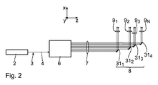
マイクロリソグラフィのための投影露光装置1は、複数の投影露光装置を含むシステムの一部であり、図1は、これらの投影露光装置のうちの1つの投影露光装置1を示している。投影露光装置1は、微細構造又はナノ構造の電子半導体構成要素を発生させるように機能する。システムの全ての投影露光装置に対して共通の光源又は放射線源2が、例えば、2nmと30nmの間、特に2nmと15nmの間の範囲の波長のEUV放射線を放出する。光源2は、自由電子レーザ(FEL)として具現化される。光源2は、非常に高い輝度を有するコヒーレント放射線を生成するシンクロトロン放射線源又はシンクロトロン放射線ベースの光源を含む。そのようなFELを記載している公報は、WO 2009/121 438 A1に示されている。使用することができる光源2は、Uwe Schindler著「電気的に切換可能なヘリシティーを有する超電導アンジュレーター(Ein supraleitender Undulator mit elektrisch umschaltbarer Helizitat)」、ヘルムホルツ協会カールスルーエ研究センター、科学報告書FZKA 6997、2004年8月、US 2007/0152171 A1、及びDE 103 58 225 B3に記載されている。
A
光源2は、生ビーム内に0.1mm2よりも小さいオリジナルエタンデュを有する。エタンデュは、光源の放出光エネルギの90%を含む最小位相空間体積である。このエタンデュに対応するエタンデュの定義は、EP 1 072 957 A2及びUS 6 198 793 B1に見出され、これらの文献は、x及びyが、照明される照明視野を張る視野寸法であり、NAが視野照明の開口数である時に、照明データx,yとNA2との乗算によって得られることを示している。光源の0.1mm2よりも一層小さいエタンデュ、例えば、0.01mm2よりも小さいエタンデュが可能である。
The
EUV光源2は、電子ビームを生成するための電子ビーム供給デバイスとEUV生成デバイスとを有する。EUV生成デバイスには、電子ビーム供給デバイスによって電子ビームが供給される。電子ビーム供給デバイスは、アンジュレーターとして具現化される。任意的にアンジュレーターは、変位によって調節可能なアンジュレーター磁石を含むことができる。アンジュレーターは、電磁石を含むことができる。光源2の場合はウィグラーを設けることができる。
The EUV
光源2は2.5kWの平均電力を有する。光源2のパルス周波数は30MHzである。各個々の放射線パルスは、83μJのエネルギを伝達する。100fsの放射線パルス長の場合に、833MWの放射線パルス電力に対応する。
The
光源2の繰り返し数は、キロヘルツ範囲では、例えば、100kHz、比較的低いメガヘルツ範囲では、例えば、3MHz、中程度のメガヘルツ範囲では、例えば、30MHz、上位メガヘルツ範囲では、例えば、300MHz、又は他にギガヘルツ範囲で例えば、1.3GHzにあるとすることができる。
The number of repetitions of the
下記では、位置関係の例示を容易にするために直交xyz座標系を使用する。通常これらの例示では、x座標は、y座標と共にEUV照明結像光3のビーム断面を張る。相応にz方向は、通常、照明結像光3のビーム方向に延びている。例えば、図2及び図12では、x方向は、投影露光装置1のシステムが収まる構成面と垂直に延びている。図4から図11の座標系は、このx方向に対してz軸の周りに90°だけ回転される。
In the following, an orthogonal xyz coordinate system is used to facilitate the illustration of the positional relationship. Usually, in these examples, the x coordinate stretches the beam cross section of the EUV
図1は、システムの投影露光装置1のうちの1つの主構成要素を非常に概略的に示している。
FIG. 1 very schematically shows one main component of a
光源2は、照明結像光3を最初にEUV生ビーム4の形態で模造する。図3は、左に1:1のx/yアスペクト比を有するEUV生ビーム4を通る断面を非常に概略的に示している。一般的に生ビーム4は、ガウス強度分布を有するビーム、すなわち、図3に破線境界線5に示す円形断面のビームとして存在する。EUV生ビーム4は、非常に小さい発散を有する。
The
ビーム成形光学ユニット6(図1を参照されたい)は、EUV生ビーム4からEUV集合出力ビーム7を発生させるように機能する。これを図1には非常に概略的に、図2にはそれよりも幾分詳細に示している。EUV集合出力ビーム7は非常に小さい発散を有する。図3は、左から第2の断面図にEUV集合出力ビーム7のアスペクト比を前と同じく指定している。このアスペクト比は、システム内部で光源2によって給光される投影露光装置1の台数Nに依存してビーム成形光学ユニット6によって予め定められる。ビーム成形光学ユニット6によって生成されるx/yアスペクト比は、ほぼ
![]()
![]()
![]()
![]()
図2は、N=4であり、従って、光源2が、図1に記載の投影露光装置1のタイプによる4台の投影露光装置に照明光3を供給するためのシステム設計を示している。N=4では、EUV集合出力ビーム7のx/yアスペクト比は2:1である。投影露光装置1の台数Nは、より大きいとすることができ、例えば、最大で10台までとすることができる。
FIG. 2 shows a system design for N = 4, so that the
別のシステム設計では、EUV集合出力ビームはN:1のx/yアスペクト比を有する。この比にも、望ましい設定値アスペクト比を乗じることができる。 In another system design, the EUV collective output beam has an x / y aspect ratio of N: 1. This ratio can also be multiplied by the desired setting aspect ratio.
出力結合光学ユニット8(図1及び図2を参照されたい)は、EUV集合出力ビーム7から複数本、すなわち、N本のEUV個別出力ビーム91から9N(i=1,...N)を発生させるように機能する。
The output coupling optical unit 8 (see FIGS. 1 and 2) has a plurality of EUV
図1は、これらの個々の出力ビーム9のうちの正確に1つのもの、すなわち、出力ビーム91の更に別の案内を示している。出力結合光学ユニット8によって生成された図1に同じく略示す他のEUV個別出力ビーム9iは、システムの他の投影露光装置に供給される。
1 are those of exactly one of these
出力結合光学ユニット8の下流では、照明結像光3は、ビーム案内光学ユニット10(図1を参照されたい)により、投影される物体としてレチクルの形態にあるリソグラフィマスク12が内部に配置された投影露光装置1の物体視野11に向けて案内される。ビーム案内光学ユニット10と共に、ビーム成形光学ユニット6及び出力結合光学ユニット8は、投影露光装置1のための照明系を構成する。
Downstream of the output coupling
ビーム案内光学ユニット10は、照明光3に対するビーム経路、すなわち、EUV個別出力ビーム9iに対するビーム経路の順番に、フォーカスアセンブリ14の形態にある入力結合光学ユニットと、下流照明光学ユニット15とを含む。照明光学ユニット15は、従来技術で公知であるものに対応する機能を有し、従って、図1には関連のEUVビーム経路なく極めて概略的にしか例示していない視野ファセットミラー16と瞳ファセットミラー17とを含む。
Beam guiding optical unit 10 includes the beam path for the
視野ファセットミラー16での反射の後に、視野ファセットミラー16の個々の視野ファセット(例示していない)に割り当てられたEUV部分ビームに分割された照明光3の使用放射線ビームは、瞳ファセットミラー17上に入射する。瞳ファセットミラー17の瞳ファセット(図1には例示していない)は円形である。視野ファセットのうちの1つと瞳ファセットのうちの1つとを含む被入射ファセット対が各場合に使用放射線ビームの関連部分ビームに対する照明チャネル又はビーム案内チャネルを予め定めるように、これらの瞳ファセットのうちの1つが、視野ファセットのうちの1つから反射される使用放射線ビームの各部分ビームに割り当てられる。視野ファセットに対する瞳ファセットのチャネル別割り当ては、投影露光装置1による望ましい照明に依存して行われる。従って、照明光3は、視野ファセットのうちのそれぞれの1つと瞳ファセットのうちのそれぞれの1つとを含む対を連続して経由する照明チャネルに沿って個々の照明角度を予め定めるように案内される。それぞれ予め定められる瞳ファセットを駆動するために、視野ファセットミラーは、各場合に個々に傾斜される。
After reflection at the
瞳ファセットミラー17を経由し、更に適切な場合に、例えば、3つのEUVミラー(例示していない)の下流伝達光学ユニットを通して、視野ファセットは、投影露光装置1の投影光学ユニット19(図1に同じく略示す)のレチクル平面又は物体平面18内の照明視野又は物体視野11に結像される。
The field facet passes through the
視野ファセットミラー16の視野ファセットの照明によって全ての照明チャネルを通して引き起こされる個々の照明角度から、照明光学ユニット15による物体視野11の照明の照明角度分布がもたらされる。
From the individual illumination angles caused through all the illumination channels by the illumination of the field facets of the
照明光学ユニット15の更に別の実施形態において、特に投影光学ユニット19の入射瞳の適切な位置を前提として、物体視野11の上流の伝達光学ユニットのミラーを省くことができ、それによって使用放射線ビームに関して投影露光装置1の照明の対応する増強が引き起こされる。
In yet another embodiment of the illumination optical unit 15, the mirror of the transmission optical unit upstream of the
使用放射線ビームを反射するレチクル12は、物体平面18内にある物体視野11の領域に配置される。レチクル12は、レチクル変位ドライブ21を用いて駆動される方式で変位可能なレチクルホルダ20によって担持される。
The
投影光学ユニット19は、物体視野11を像平面23の像視野22に結像する。投影露光中に、この像平面23内に、投影露光中に投影露光装置1によって露光される感光層を担持するウェーハ24が配置される。ウェーハ24は、この場合はウェーハ変位ドライブ26を用いて制御される方式で変位可能なウェーハホルダ25によって担持される。
The projection
投影露光中に、図1のレチクル12とウェーハ24の両方が、レチクル変位ドライブ21とウェーハ変位ドライブ26との対応する駆動によってx方向と同期方式で走査される。ウェーハは、投影露光中に一般的に600mm/sの走査速度でx方向に走査される。
During projection exposure, both the
図4及び図5は、ビーム成形光学ユニット6の実施形態を示している。図4及び図5に記載のビーム成形光学ユニット6は、照明光3が入射する順番に順次番号が振られた合計で4つのミラーBS1、BS2、BS3、及びBS4を有する。図4は、xz平面と平行な図にビーム成形光学ユニット6を示している。図5は、yz平面と平行な平面図にビーム成形光学ユニット6を示している。
4 and 5 show an embodiment of the beam shaping
図4及び図5のビーム成形光学ユニット6のミラーBS1からBS4によるビーム偏向の例示は、図4のミラーMS1及びBS4、並びに図5のミラーBS2及びBS3が、各場合に両方のミラーを反射面が観察者に向く平面図内に示すことに限って現実からずれている。実際には、図4のミラーBS4の反射面及び図5のミラーBS3の反射面は観察者から逸れている。
An example of beam deflection by the mirrors BS1 to BS4 of the beam shaping
照明光3は、ミラーBS1からBS4の全ての上にかすめ入射で入射する。かすめ入射は、照明光3の入射又は反射の主方向と、照明光3が入射するそれぞれのミラーの反射面セクションに対する法線Nとの間の入射角αが60°よりも大きい場合に存在する。入射角αは、例えば、65°よりも大きいとすることができ、70°よりも大きいとすることができ、75°よりも大きいとすることができる。
The
図4及び図5に記載のビーム成形光学ユニット6は、2つのビーム成形ミラー群27、28、すなわち、最初に図4に271及び272によっても表記しているミラーBS1及びBS4を含むビーム成形ミラー群27と、図5に281及び282によっても表記しているミラーBS2及びBS3を含むビーム成形ミラー群28とを有する。各ミラー群27、28は、共通の群入射平面を有する。ミラー群27の入射平面は、yz平面(図5の作図面)と平行である。ミラー群28の入射平面は、xz平面(図4の作図面)と平行である。従って、ミラー群27、28の2つの群入射平面yzとxzとは、互いに異なり、図示の実施形態では互いに対して垂直である。
The beam shaping
ビーム成形ミラー群27は、yz平面におけるEUV集合出力ビーム7のビーム成形のためなどに機能する。ビーム成形ミラー群28は、xz平面におけるEUV集合出力ビーム7のビーム成形のためなどに機能する。
The beam shaping mirror group 27 functions for beam shaping of the EUV
一方でビーム成形ミラー群27と、他方で28とは、原理的にガリレオ円筒形望遠鏡の効果を有する。例えば、ガウス強度分布を有する実質的に円形の生ビーム4から矩形使用断面の範囲に均一な強度分布を有する実質的に矩形のEUV集合出力ビーム7へのビームプロファイルの再成形をもたらすために、ビーム成形ミラー群27及び/又は28のミラーの少なくとも一部に、自由形プロファイルを与えることができ、すなわち、これらのミラーは、反射面として自由曲面を有することができる。自由形プロファイルは、円錐形として表すことができない高さ分布である。この場合の円錐は、2つの直交方向に異なる円錐によって表される面形状を意味するとも理解しなければならず、そのような面形状の一例は円柱である。自由形プロファイルは、そのような円錐形によっても表すことができない。ビーム成形光学ユニット6の1又は2以上のミラーの高さ分布の偏差は、1マイクロメートル(μm)よりも大きく、特に5マイクロメートルよりも大きく、特に20マイクロメートルよりも大きいとすることができる。
On the other hand, the beam shaping mirror group 27 and the other 28 have the effect of a Galileo cylindrical telescope in principle. For example, to provide a reshaping of the beam profile from a substantially circular
ミラーBS2及びBS3を含むミラー群28は、全体的に更に別のミラー群27の最初のミラーBS1の下流で、この更に別のミラー群27の第2かつ最後のミラーBS4の上流のビーム経路に配置される。
The
ビーム成形光学ユニット6の実施形態に基づいて、照明光3の入射角は、ミラー群27、28の一方のものの全てのミラー上で同じ大きさとすることができ、又はミラー群27、28の一方のものの少なくとも2つのミラー上で異なる大きさとすることができる。この関連において、入射角は、EUV生ビーム4内で中心を進む光線の入射角を意味すると理解しなければならない。
Based on the embodiment of the beam shaping
ミラーBS1は、x軸と平行に延びる円柱軸を有する凸円筒形ミラーとして具現化される。ミラーBS2は、y軸と平行に延びる円柱軸を有する凸円筒形ミラーとして具現化される。ミラーBS3は、y軸と平行に延びる円柱軸を有する凹円筒形ミラーとして具現化される。ミラーBS4は、x軸と平行に延びる円柱軸を有する凹円筒形ミラーとして具現化される。 The mirror BS1 is embodied as a convex cylindrical mirror having a cylindrical axis extending parallel to the x axis. The mirror BS2 is embodied as a convex cylindrical mirror having a cylindrical axis extending parallel to the y axis. The mirror BS3 is embodied as a concave cylindrical mirror having a cylindrical axis extending parallel to the y-axis. The mirror BS4 is embodied as a concave cylindrical mirror having a cylindrical axis extending parallel to the x axis.
ミラー群27は、x座標軸に、ミラー群28のy座標軸の拡大効果と比較して2倍の生ビームのビーム直径の拡大を可能にする。更に、2つのミラー群27、28は、EUV集合出力ビーム7の矩形の断面プロファイルを成形するように機能する。
The mirror group 27 allows the beam diameter of the raw beam to be expanded on the x coordinate axis by a factor of two compared to the expansion effect of the y coordinate axis of the
図6から図11は、ビーム成形光学ユニット6の更に別の実施形態を示している。これらの実施形態は、様々なビーム成形ミラーBSi(i=1,...)によって生成される偏向角の順序が異なる。従って、図6から図11では、各場合にミラー自体を物理的に示さず、ミラーBSiの偏向効果のみを示している。
6 to 11 show still another embodiment of the beam shaping
図6及び図7に記載のビーム成形光学ユニットの実施形態6は、ミラーBS1からBS4上の照明光3の入射角に関して、更にミラー群27、28へのミラーBS1からBS4の割り当てに関しても図4及び図5に記載の実施形態に対応する。ミラーBS1からBS4における照明光3の入射角αは、図6及び図7に記載の実施形態の場合の全てのこれらのミラーに関して等しい。従って、EUV集合出力ビーム7の主ビーム方向は、ビーム成形光学ユニット6内に入射するEUV生ビーム4の主ビーム方向に等しい。
図8及び図9は、図4から図7に記載のビーム成形光学ユニット6の代わりに使用することができるビーム成形光学ユニットの更に別の実施形態29を示している。ビーム成形光学ユニット6を参照して上述したものに対応する構成部分及び機能は、ビーム成形光学ユニット29の場合にも同じ参照符号を伴い、これらに対して再度詳細に解説することはしない。
8 and 9 show yet another
ビーム成形光学ユニット6とは対照的に、ビーム成形光学ユニット29の場合は、ミラーBS1からBS4上でEUV放射線の異なる入射角α、βが存在する。ミラーBS1及びBS2は、各場合に、第3のミラーBS3に至るまでのビーム成形光学ユニット29のビーム経路が、ビーム成形光学ユニット6内のビーム経路に対応するように入射角αで反射する。ミラーBS3及びBS4において、照明光3は、入射角αと比較して小さい入射角βではあるが、それにも関わらずかすめ入射で反射される。この反射は、ビーム成形光学ユニット29から射出するEUV集合出力ビーム7の主ビーム方向がz方向と平行に延びず、xz平面とyz平面の両方において、z方向と平行に延びる入射方向に対してゼロとは異なる角度を形成するという効果を有する。
In contrast to the beam shaping
ビーム成形光学ユニット29の最後の2つのミラーBS3及びBS4における小さめの入射角βは、これらの最後の2つのミラーBS3及びBS4の構造的に小さめの実施形態、すなわち、小さい広がりの反射面を有する実施形態を可能にする。この実施形態は、これらの最後のミラーBS3及びBS4の場所では、照明光は入射EUV生ビームと比較して断面が既にかなり拡大されているので、2つの先頭のミラーBS1及びBS2よりもビーム成形光学ユニット29のこれらの最後の2つのミラーBS3及びBS4に対してより大きい意味を有する。
The smaller angle of incidence β in the last two mirrors BS3 and BS4 of the beam shaping
図10及び図11は、ビーム成形光学ユニット6、29の代わりに使用することができるビーム成形光学ユニットの更に別の実施形態30を示している。ビーム成形光学ユニット6、29を参照して上述したものに対応する構成部分及び機能は、ビーム成形光学ユニット30の場合にも同じ参照符号を伴い、これらに対して再度詳細に解説することはしない。
10 and 11 show yet another
ビーム成形光学ユニット30は、その中で前と同じく照明光3が入射する順番に順次番号が振られた合計で5つのミラーBS1、BS2、BS3、BS4、BS5を有する。ミラーBS1、BS2及びBS5は、yz入射平面を有するビーム成形光学ユニット30の最初のミラー群27に属する。残りの2つのミラーBS3及びBS4は、xz入射平面を有するミラー群28に属する。
The beam shaping
最初のミラーBS1での反射の後に、ビーム成形光学ユニット30内の照明光3のビーム経路は、ビーム成形光学ユニット29内のものに対応し、この場合に、ビーム成形光学ユニット30のミラーBS2からBS5は、ビーム成形光学ユニット29のミラーBS1からBS4の機能を有する。
After reflection at the first mirror BS1, the beam path of the
照明光3、すなわち、EUV生ビーム4は、ビーム成形光学ユニット30の最初のミラーBS1上に強いかすめ入射で入射する。従って、ビーム成形光学ユニット30の最初のミラーBS1上での照明光3の入射角γは、入射角αよりも大きい。入射角γは、一方でミラーBS1とBS2の間に、他方でミラーBS5の下流に照明光3によって出現するyz平面における照明光3のビーム方向差を正確に補償し、それによってビーム成形光学ユニット30から射出した後のyz平面内の照明光3の主ビーム方向が、ビーム成形光学ユニット30への入射時のyz平面内の主ビーム方向と平行であり、すなわち、z方向と平行であるような大きさを有する。
The
ビーム成形光学ユニット30の上流及び下流において、照明光3は、内部にシステムが含まれる建物の天井と平行に進む。
Upstream and downstream of the beam shaping
個々のミラー271(BS1)、272(BS2)、及び273(BS5)が異なる入射角、すなわち、γ、α、及びβを内部で有するビーム成形光学ユニット30のミラー群27の群入射平面yz上に投影した場合に、ビーム成形光学ユニット30によって生成されたEUV集合出力ビーム7は、ビーム成形光学ユニット30内に入射するEUV生ビーム4と同じ方向、すなわち、z方向に進む。
Group incidence of the mirror group 27 of the beam shaping
ビーム成形光学ユニット6及び30の最後のミラーBS4及びBS5の反射面の典型的な断面寸法は、それぞれ1mから1.5mであり、一般的にこれらのミラーは、第一近似として矩形である反射面を有し、指定断面寸法は、2つの軸のうちの長い方に関するものである。ビーム成形光学ユニットの最初のミラーBS1の反射面の典型的な断面寸法は20mmから100mmである。
Typical cross-sectional dimensions of the reflecting surfaces of the last mirrors BS4 and BS5 of the beam shaping
ビーム成形光学ユニット6又は30を射出した後に、EUV集合出力ビーム7の光線は実質的に平行に進む。EUV集合出力ビーム7の発散は、10mradよりも小さく、特に1mradよりも小さく、特に100μradよりも小さく、特に10μradよりも小さいとすることができる。
After exiting the beam shaping
図2及び図12は、EUV集合出力ビーム7からEUV個別出力ビーム9を発生させるための出力結合光学ユニット8の例を示している。出力結合光学ユニットは、EUV個別出力ビーム91、92、...に割り当てられ、これらのビームをEUV集合出力ビーム7から脱結合する複数の出力結合ミラー311、312、...を有する。図2は、照明光3が、脱結合中に出力結合ミラー31によって90°だけ偏向されるような出力結合ミラー31の配置を示している。出力結合ミラー31が、図12に略示するような照明光3のかすめ入射を用いて作動される実施形態が好ましい。図2に記載の実施形態において、出力結合ミラー31上での照明光3の入射角αは約70°であるが、それを有意に超えることさえ可能であり、それぞれの出力結合ミラー31によるEUV個別出力ビーム9の有効な偏向が、EUV集合出力ビーム7の入射方向と比較して10°であるように、例えば、85°の領域内にあるとすることができる。
FIGS. 2 and 12 show an example of the output coupling
出力結合ミラー31iの各々は、ヒートシンク(詳細には例示していない)に熱結合される。 Each of the output coupling mirrors 31 i is thermally coupled to a heat sink (not illustrated in detail).
図2は、合計で4つの出力結合ミラー311から314を有する。図12は、合計で3つの出力結合ミラー311から313を有する出力結合光学ユニット8の変形を示している。例えばN=2又はN≧4、特にN≧8等、光源2によって給光される投影露光装置1の台数Nに依存して異なる個数Nの出力結合ミラー31も可能である。
FIG. 2 has a total of four output coupling mirrors 31 1 to 31 4 . FIG. 12 shows a modification of the output coupling
脱結合後に、EUV個別出力ビーム9の各々は、

出力結合ミラー31i(i=1,2,...)は、それぞれの最近接出力結合ミラー31iが、EUV集合出力ビーム7の辺縁断面部分を反射し、それによってこの断面部分をこの出力結合ミラー31iのそばを通過する残りのEUV集合出力ビーム7から脱結合するように、EUV集合出力ビーム7のビーム経路にEUV集合出力ビーム7のビーム方向に縦列偏差方式で配置される。縁部からのこの出力結合は、EUV集合出力ビーム7のそれにも関わらず残っている最後の断面部分が脱結合されるまで、その後の出力結合ミラー31 i+1 ,...によって繰り返される。
The output coupling mirrors 31 i (i = 1, 2,...) Are such that each closest output coupling mirror 31 i reflects a marginal cross-section portion of the EUV
EUV集合出力ビーム7の断面内では、y軸と平行に、すなわち、EUV集合出力ビーム7のx/y矩形断面の短辺と平行に延びる分離線32上で、EUV個別出力ビーム9iに割り当てられた断面部分の間の分離が実施される。EUV個別出力ビーム9iの分離は、各場合にビーム経路内の次の光学構成部分から最も離れている断面部分が切り離されるように実施される。それによって取りわけ出力結合光学ユニット8の冷却が容易になる。
In the cross section of the EUV
照明光3のビーム経路内で出力結合光学ユニット8の下流にある偏向光学ユニット13は、第1にEUV個別出力ビーム9が各場合にこの偏向光学ユニット13の下流で垂直ビーム方向を有するようにEUV個別出力ビーム9を偏向するために、第2に、EUV個別出力ビーム9のx/yアスペクト比を図3の右端に示すような1:1のx/yアスペクト比に適応させるように機能する。このアスペクト比寄与にも、望ましい設定値アスペクト比を乗じることができる。従って、上述のx/yアスペクト比は、設定値アスペクト比、例えば、矩形又は弓形の物体視野のアスペクト比が乗じられて望ましい実際のアスペクト比をもたらすアスペクト比寄与である。上述のx/y設定値アスペクト比は、照明光学ユニット15の最初の光学要素のアスペクト比とすることができる。上述のx/y設定値アスペクト比は、照明光学ユニット15の中間フォーカス42における照明光3の角度のアスペクト比とすることができる。
The deflection
EUV個別出力ビーム9の垂直ビーム経路が出力結合光学ユニット8の下流に既に存在する場合に、偏向光学ユニット13の偏向効果を省くことができ、EUV個別出力ビーム9のx/yアスペクト比に関する適応効果で十分である。
When the vertical beam path of the EUV
偏向光学ユニット13の下流のEUV個別出力ビーム9は、適切な場合はフォーカスアセンブリ14を通した後に、照明光学ユニットの効率的な折り返しを可能にする角度で照明光学ユニット15内に入射するように進むことができる。偏向光学ユニット13の下流では、EUV個別出力ビーム9iは、垂直に対して0°から10°までの角度、垂直に対して10°から20°までの角度、又は垂直に対して20°から30°までの角度で進むことができる。
The EUV
下記では、偏向光学ユニット13に関する様々な変形を図13から図19を参照して説明する。この場合に、照明光3を単一光線として略示し、すなわち、ビーム例示を省いている。
In the following, various modifications relating to the deflection
偏向光学ユニットを通した後のEUV個別出力ビーム9iの発散は、10mradよりも小さく、特に1mradよりも小さく、特に100μradよりも小さく、すなわち、EUV個別出力ビーム9iのビーム内の任意の2つの光線の間の角度が20mradよりも小さく、特に2mradよりも小さく、特に200μradよりも小さい。これは、下記で説明する変形に対して満たされる。
The divergence of the EUV
図13に記載の偏向光学ユニット13は、脱結合されたEUV個別出力ビーム9を全体的に約75°の偏向角で偏向する。従って、EUV個別出力ビーム9は、図13に記載の偏向光学ユニット13上に、水平(xy平面)に対して約15°の角度で入射し、偏向光学ユニット13を図13のx軸と平行なビーム方向で射出する。偏向光学ユニット13は、EUV個別出力ビーム9に対して約55%の全伝達率を有する。
The deflecting
図13に記載の偏向光学ユニット13は、ビーム経路内で照明光3が入射する順番に順次番号が振られた合計で6つの偏向ミラーD1、D2、D3、D4、D5、及びD6を有する。偏向ミラーD1〜D6から、各場合にこれらの反射面を通る一セクションのみを略示しており、それぞれの反射面の曲率を有意に誇張して例示している。照明光3は、図13に記載の偏向光学ユニット13の全てのミラーD1からD6上に、xz平面と平行な共通の偏向入射平面内でかすめ入射で入射する。
The deflection
ミラーD1及びD2は、y軸と平行な円柱軸を有する凸円柱ミラーとして具現化される。ミラーD3は平面ミラーとして具現化される。ミラーD4からD6は、ここでもまた、y軸と平行な円柱軸を有する凹円柱ミラーとして具現化される。 The mirrors D1 and D2 are embodied as convex cylindrical mirrors having a cylindrical axis parallel to the y axis. The mirror D3 is embodied as a plane mirror. The mirrors D4 to D6 are again embodied as concave cylindrical mirrors having a cylindrical axis parallel to the y-axis.
凸円柱ミラーをドーム形ミラーとも呼ぶ。凹円柱ミラーを皿形ミラーとも呼ぶ。 A convex cylindrical mirror is also called a dome-shaped mirror. A concave cylindrical mirror is also called a dish-shaped mirror.
ミラーD1からD6の組合せビーム成形効果は、x/yアスペクト比が、値
![]()
![]()
偏向ミラーD1からD6のうちの少なくとも1つ、又は他に偏向ミラーD1からD6の全ては、割り当てアクチュエータ34を用いてx方向及び/又はz方向に変位可能なものとして具現化することができる。その結果、偏向光学ユニット13の第1に偏向効果の適応を第2にアスペクト比適応効果の適応をもたらすことができる。これに代えて又はこれに加えて、偏向ミラーD1からD6のうちの少なくとも1つをその曲率半径に関して適応可能なミラーとして具現化することができる。この目的のために、それぞれのミラーD1からD6をこの図面には例示していないアクチュエータシステムによって互いに対して変位可能な複数の個々のミラーから構成することができる。
At least one of the deflection mirrors D1 to D6, or else all of the deflection mirrors D1 to D6, can be embodied as displaceable in the x and / or z direction using the assigning
投影露光装置1を含むシステムの様々な光学アセンブリは、適応的に具現化することができる。従って、光源2からのEUV個別出力ビーム9iを投影露光装置1のうちの何台に供給するように意図するかということと共に、それぞれの偏向光学ユニット13を通した後のそれぞれのEUV個別出力ビーム9に関してどのようなエネルギ比及びどのようなビーム幾何学形状が存在するように意図するかということを中心的に予め定めることができる。所定値に基づいて、EUV個別出力ビーム9iは、その強度及びその設定値x/yアスペクト比が異なることができる。特に、出力結合ミラー31iを適応可能に設定することによってEUV個別出力ビーム9iのエネルギ比を変更することができ、偏向光学ユニット13を適応可能に設定することにより、偏向光学ユニット13を通した後のEUV個別出力ビーム9iのサイズ及びアスペクト比を不変に保つことができる。
The various optical assemblies of the system including the
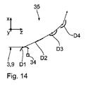
N台の投影露光装置1を含むシステム内で図13に記載の偏向光学ユニット13の代わりに使用することができる偏向光学ユニットの更に別の実施形態を図14から図19を参照して以下に説明する。図1から図13、特に図13を参照して上述した構成部分及び機能は同じ参照符号を伴い、これらに対して再度詳細に解説することはしない。
Still another embodiment of a deflection optical unit that can be used in place of the deflection
図14に記載の偏向光学ユニット35は、照明光3のビーム経路に合計で4つのミラーD1、D2、D3、D4を有する。ミラーD1は、凸円柱ミラーとして具現化される。ミラーD2からD4は、凹円柱ミラーとして具現化される。
The deflection
より詳細な光学データを下記の表から達成することができる。この場合に、最初の列は、それぞれのミラーD1からD4の曲率半径を表し、第2の列は、それぞれのミラーD1からD3とそれぞれのその後のミラーD2からD4との間の距離を表している。この距離は、対応する反射の間でEUV個別出力ビーム9i内の中心光線が進む距離に関するものである。この表及びその後の表に使用する単位は、別途記載しない限り各場合にmmである。この場合のEUV個別出力ビーム9iは、偏向光学ユニット13内に10mmの半直径d in /2を用いて入射する。
図14に記載の偏向光学ユニット35は、x/yアスペクト比を3倍拡大する。
The deflection
図15は、同じく4つのミラーD1からD4を含む偏向光学ユニットの更に別の実施形態36を示している。ミラーD1は、凸円柱ミラーである。ミラーD2は平面ミラーである。ミラーD3とD4とは、等しい曲率半径を有する2つの円柱ミラーである。
FIG. 15 shows a
より詳細な光学データをレイアウトに関して図14に関する表に対応する下記の表から達成することができる。
図15に記載の偏向光学ユニット35は、EUV個別出力ビーム9のx/yアスペクト比を2倍拡大する。
The deflection
図16は、5つのミラーD1からD5を含む偏向光学ユニットの更に別の実施形態37を示している。最初のミラーD1は、凸円柱ミラーである。第2のミラーD2は平面ミラーである。更に別のミラーD3からD5は、3つの凹円柱ミラーである。
FIG. 16 shows a
より詳細なデータをレイアウトに関して図14及び図15に関する表に対応する以下の表から達成することができる。
図16に記載の偏向光学ユニット37は、EUV個別出力ビーム9のx/yアスペクト比を5倍拡大する。
The deflection
偏向光学ユニット37の更に別の実施形態は、以下の表に示す曲率半径及びミラー距離においてのみ図16に記載の実施形態と異なる。
図16に記載の第1の実施形態とは対照的に、この代替設計は、x/yアスペクト比に関して4という拡大率を有する。 In contrast to the first embodiment described in FIG. 16, this alternative design has a magnification factor of 4 with respect to the x / y aspect ratio.
偏向光学ユニットの更に別の実施形態37は、以下の表に示す曲率半径及びミラー距離において図16に記載の実施形態と異なる。
上記で記述した実施形態とは対照的に、この更に別の代替設計は、x/yアスペクト比に関して3という拡大率を有する。最後の2つのミラーD4及びD5の曲率半径は等しい。 In contrast to the embodiment described above, this further alternative design has a magnification factor of 3 with respect to the x / y aspect ratio. The last two mirrors D4 and D5 have the same radius of curvature.
図17は、6つのミラーD1からD6を含む偏向光学ユニット38の更に別の実施形態を示している。最初のミラーD1は、凸円柱ミラーである。次の2つの偏向ミラーD2、D3は、各場合に等しい曲率半径を有する凹円柱ミラーである。次の偏向ミラーD4は平面ミラーである。偏向光学ユニット38の最後の2つの偏向ミラーD5、D6は、再度等しい曲率半径を有する凹円柱ミラーである。
FIG. 17 shows a further embodiment of the deflection
より詳細なデータをレイアウトに関して図16に関する表に対応する以下の表から達成することができる。
偏向光学ユニット38は、x/yアスペクト比に関して5という拡大率を有する。
The deflection
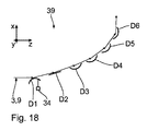
図18は、6つのミラーD1からD6を含む偏向光学ユニットの更に別の実施形態39を示している。偏向光学ユニット39の最初のミラーD1は、凸円柱ミラーである。下流にある第2の偏向ミラーD2は平面ミラーである。下流にある偏向ミラーD3からD6は、各場合に凹円柱ミラーである。一方でミラーD3及びD4の曲率半径と、他方でミラーD5及びD6の曲率半径とは等しい。
FIG. 18 shows a
より詳細なデータをレイアウトに関して図17に関する表に対応する以下の表から達成することができる。
偏向光学ユニット39は、x/yアスペクト比に関して5という拡大率を有する。
The deflection
図18に関する代替設計では、凸/平面/凹/凹/凹/凹というミラー順序は、上記で記述した偏向光学ユニット39の実施形態の場合と正確に同じである。図18に関するこの代替設計は、以下の表によって例示するように、特定の曲率半径及びミラー距離が異なる。
図18に関するこの代替設計は、EUV個別出力ビーム9のx/yアスペクト比に関して4という拡大率を有する。
This alternative design for FIG. 18 has a magnification factor of 4 with respect to the x / y aspect ratio of the EUV
図19は、6つのミラーD1からD6を含む偏向光学ユニットの更に別の実施形態40を示している。偏向光学ユニット40の最初の偏向ミラーD1は、凸円柱ミラーである。2つの下流偏向ミラーD2及びD3は平面ミラーである。偏向光学ユニット40の下流偏向ミラーD4からD6は、凹円柱ミラーである。最後の2つの偏向ミラーD5及びD6の曲率半径は等しい。
FIG. 19 shows a
より詳細なデータをレイアウトに関して図18に関する表に対応する以下の表から達成することができる。
偏向光学ユニット40は、x/yアスペクト比に関して5という拡大率を有する。
The deflection
更に別の変形(例示していない)では、偏向光学ユニットは、合計で8つのミラーD1からD8を有する。EUV個別出力ビーム9のビーム経路にある2つの先頭偏向ミラーD1及びD2は、凹円柱ミラーである。4つの下流偏向ミラーD3からD6は、凸円柱ミラーである。この偏向光学ユニットの最後の2つの偏向ミラーD7及びD8は再度凹円柱ミラーである。
In yet another variant (not illustrated), the deflection optical unit has a total of eight mirrors D1 to D8. The two leading deflection mirrors D1 and D2 in the beam path of the EUV
これらのミラーD1からD8は、図13のミラーD1と同様な方式でアクチュエータ34に接続され、これらのアクチュエータによって隣接ミラーD1からD8の間の距離を予め定めることができる。
These mirrors D1 to D8 are connected to the
以下の表は、8つのミラーD1からD8を含むこの偏向光学ユニットの設計を示しており、曲率半径に加えて、射出EUV個別出力ビーム9iの様々な半直径dout/2に関するミラー距離も示している。この場合に、EUV個別出力ビームは、8つのミラーD1からD8を含む偏向光学ユニット内に10mmの半直径din/2を用いて入射し、図示の距離値に基づいて、偏向を受けるEUV個別出力ビーム9iのx/yアスペクト比に関して4.0、4.5、及び5.0という拡大率を提供する。
偏向光学ユニットの更に別の実施形態(同じく例示していない)では、4つのミラーD1からD4が存在する。EUV個別出力ビーム9iのビーム経路内の最初のミラーD1及び第3のミラーD3は、凹円柱ミラーとして具現化される。以下の表は、曲率半径に加えて、10mmのEUV個別出力ビーム9iの入力半直径din/2に関して計算した距離値、すなわち、4つのミラーD1からD4を含むこの偏向群を通過する時にx/yアスペクト比に関して1.5(半直径dout/2 15mm)、1.75(半直径dout/2 17.5mm)、及び2.0(半直径dout/2 20mm)という拡大率をもたらす距離値も示している。
偏向光学ユニット13は、平行な入射光が偏向光学ユニットを再び平行に射出するように設計することができる。偏向光学ユニット13に平行入射で入射したEUV個別出力ビーム9iの光線方向の偏角は、偏向光学ユニットを射出した後に、10mradよりも小さく、特に1mradよりも小さく、特に100μradよりも小さいとすることができる。
The deflection
偏向光学ユニット13のミラーDiは、屈折力を持たないように、すなわち、平面方式に具現化することができる。この平面方式での具現化は、特に、Nが、光源2によって給光される投影露光装置1の台数である時に、EUV集合出力ビーム7のx/yアスペクト比がN:1のアスペクト比を有する場合に可能である。このアスペクト比に、望ましい設定値アスペクト比を乗じることができる。
The mirror Di of the deflecting
屈折力を持たないミラーDiの偏向光学ユニット13は、3個から10個のミラー、特に4個から8個のミラー、特に4個又は5個のミラーで構成することができる。
The deflecting
光源2は、直線偏光光を放出することができ、偏向光学ユニット13のミラー上に入射するときの照明光3の偏光方向、すなわち、電界強度ベクトルの方向は、入射平面に対して垂直とすることができる。屈折力を持たないミラーDiの偏向光学ユニット13は、3個よりも少ないミラー、特に1個のミラーで構成することができる。
The
ビーム案内光学ユニット10内には、それぞれのEUV個別出力ビーム9のビーム経路内のそれぞれの偏向光学ユニットの下流に、入力結合光学ユニットとも表記するフォーカスアセンブリ41が配置される。
In the beam guiding optical unit 10, a
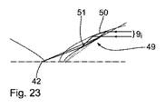
図20は、EUV個別出力ビーム9iのうちの1つに対する入力結合光学ユニット41の機能を略示している。フォーカスアセンブリ41は、それぞれのEUV個別出力ビーム9iをビーム案内光学ユニット10の中間フォーカス42に伝達する。中間フォーカス42は、照明光3に対する貫通開口部43の場所に配置される。貫通開口部43は、投影露光装置1を含むシステムが内部に含まれる建物の天井に具現化することができる。天井は、図1にも示すビーム案内光学ユニット10の中間焦点面44内で延びている。
FIG. 20 schematically shows the function of the input coupling
フォーカスアセンブリ41は、中心主光線CRに対して約10°の有効偏向角を有する。
The
別の構成では、δが中間フォーカス42における中心主光線と周辺光線の間の角度である時に、フォーカスアセンブリ41は、中心主光線CRに対してδ/2とδの間の有効偏向角を有する。δの正弦値を中間フォーカス42における放射線3の開口数(NA)とも呼ぶ。
In another configuration, the
図21は、図20に記載のフォーカスアセンブリ41の代わりに使用することができる代替フォーカスアセンブリ45のフォーカス効果を示している。フォーカスアセンブリ41とは対照的に、フォーカスアセンブリ45は、入射EUV個別出力ビーム9iの全ての個々の光線をxz入射平面内で同じ偏向方向、すなわち、負のy値に向けて偏向する。図21の左端に示すEUV個別出力ビーム9iのフォーカス個々の光線46の最小偏向角を図21ではαで表記しており、αは5°又はそれよりも小さい。
FIG. 21 illustrates the focus effect of an
フォーカスアセンブリ45は、中心主光線CRに対して約20°の有効偏向角を有する。
The
別の構成では、δが中間フォーカス42における中心主光線と周辺光線の間の角度である時に、フォーカスアセンブリ45は、中心主光線CRに対してδ/2とδの間の有効偏向角を有する。
In another configuration, the
フォーカスアセンブリ41又は45に対して使用することができるフォーカスアセンブリに関する実施形態変形を図22から図25を参照して以下に説明する。
An embodiment variant relating to the focus assembly that can be used for the
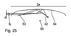
図22から図25は、各場合に、関わっているミラー反射面を通る子午断面を示している。これらのミラー面の使用反射部分を太線で強調表示している。それぞれのミラーの形状特徴に関する楕円面双曲面/放物面の面設計を解説するために、母材面切欠き部を細線で同じく描示している。 22 to 25 show meridional sections through the mirror reflection surfaces involved in each case. Use reflection portions of these mirror surfaces are highlighted with bold lines. In order to explain the elliptical hyperboloid / parabolic surface design for the shape characteristics of each mirror, the notch of the base material surface is also drawn with thin lines.
図22に記載のフォーカスアセンブリ46は、それぞれのEUV個別出力ビーム9iのビーム経路内で下流に配置された2つのミラー、すなわち、先頭の楕円面ミラー47と下流の双曲面ミラー48とを有する。
The
フォーカスアセンブリ46の場合に、EUV個別出力ビーム9iの中心主光線CRに対する有効偏向角は約50°である。フォーカスアセンブリ46の場合に、2つのミラー47及び48での反射時の中心主光線CRに対する偏向角は加算される。
In the case of the
ミラー47及び48は、凹ミラーとして具現化される。フォーカスアセンブリ46は、I型ウォルターコレクターの方式に具現化される。様々なタイプのウォルターコレクターに関する情報は、H.Wolter著「X線に対する結像光学ユニットとしてのかすめ入射ミラーシステム(Spiegelsysteme streifenden Einfalls als abbildende Optiken fur Rontgenstrahlen)」、アナーレンデアフィジーク第10巻、94ページから114ページ、1952年に見出すことができる。
The
代替構成では、フォーカスアセンブリ46の場合のEUV出力ビーム9iの中心主光線CRに対する有効偏向角は、40°よりも小さく、特に30°よりも小さく、特に15°よりも小さく、特に10°よりも小さい。
In an alternative configuration, the effective deflection angle of the
代替構成では、フォーカスアセンブリ46の場合のEUV出力ビーム9iの中心主光線CRに対する有効偏向角は、中間フォーカス42における中心主光線CRと周辺光線の間の角度の2倍よりも小さい。
In an alternative configuration, the effective deflection angle of the
図23に記載のフォーカスアセンブリ49も同じく2つのミラー、すなわち、先頭の楕円面ミラー50と下流の双曲面ミラー51とを含む。
Similarly, the
ミラー50は、凹のものであり、ミラー51は、凸のものである。
The
フォーカスアセンブリ49の場合に、ミラー50及び51での反射時の中心主光線CRに対する偏向角は減算される。
In the case of the
フォーカスアセンブリ49の場合に、主光線CRに対する有効偏向角は約30°である。
In the case of the
フォーカスアセンブリ49は、II型のウォルターコレクターの方式に具現化される。
The
代替構成では、フォーカスアセンブリ49は、主光線CRに対して最大で20°、特に最大で15°、特に最大で10°の有効偏向角を有する。
In an alternative configuration, the
フォーカスアセンブリ49の1つの構成では、主光線CRに対する有効偏向角は、中間フォーカス42における主光線CRと周辺光線の間の角度の2倍よりも小さい。
In one configuration of the
図24に記載のフォーカスアセンブリ52もまた、EUV個別出力ビーム9iのビーム経路に経路の流れに沿って配置された2つのミラー、すなわち、先頭の放物面ミラー53と下流の楕円面ミラー54とを有する。
The
ミラー53は、凸のものであり、ミラー54は、凹のものである。
The
フォーカスアセンブリ52の場合に、ミラー53及び54での反射時の中心主光線CRに対する偏向角は減算される。
In the case of the
フォーカスアセンブリ52の場合に、主光線CRに対する有効偏向角は約50°である。
In the case of the
フォーカスアセンブリ52は、III型のウォルターコレクターの方式に具現化される。
The
図25は、同じくIII型のウォルターコレクターの方式に具現化されるフォーカスアセンブリの更に別の実施形態52を示している。図21から図24に記載のフォーカスアセンブリ、特に図24に記載のフォーカスアセンブリを参照して上述した構成部分及び機能は同じ参照符号を伴い、これらに対して再度詳細に解説することはしない。
FIG. 25 shows yet another
EUV個別出力ビーム9iの出力発散は、中間フォーカス42におけるEUV個別出力ビーム9iの開口数NAによって予め定められる。この開口数NAに基づいて、図25に記載のフォーカスアセンブリの伝達率Tに対して近似的に次式を指定することができる。
T=1−0.9NA
The output divergence of EUV
T = 1-0.9NA
この場合に、開口数NAは、中間フォーカス42における主光線と周辺光線の間の角度の正弦値として定められる。同等な定義は、NAがビーム発散の半分の正弦値であると説明する。
In this case, the numerical aperture NA is determined as a sine value of the angle between the principal ray and the peripheral ray at the
楕円面ミラー54の反射面を説明する楕円面の長半軸は長さaを有する。フォーカスアセンブリ55に必要とされる構造空間2aは、2aという典型的な寸法を有する。
The major axis of the ellipsoid describing the reflecting surface of the
典型的な構造空間寸法2aは、フォーカスアセンブリ55内への入射時のEUV個別出力ビーム9iのビーム直径dの約50倍である。この比は、中間フォーカス42における開口数NAに極めて弱くしか依存しない。
A typical
楕円面ミラー54の反射面の典型的な寸法も同じくaである。楕円面ミラー54の反射面の1.4mの典型的な広がりが与えられる場合に、ビーム直径dに対して約60mmの直径が続く。
The typical dimension of the reflecting surface of the
楕円面ミラー54は短半軸bを有する。この短半軸bは、図25の作図面に対して垂直である。半軸比b/aに関して、次式が成り立つ。
b/a〜0.8NA
The
b / a-0.8NA
この場合に、NAは中間フォーカス42における開口数である。
In this case, NA is the numerical aperture at the
放物面ミラー52は焦点距離fを有する。楕円面ミラー54の長半軸aと放物面ミラーの焦点距離fとの比に関して次式が成り立つ。
a/f>50
The
a / f> 50
投影露光装置1を用いた微細又はナノ構造化構成要素の生成中に、最初にレチクル12とウェーハ24とが与えられる。その後に、投影露光装置1を用いてレチクル12上の構造が、ウェーハ24の感光層上に投影される。感光層の現像により、ウェーハ24上に微細構造又はナノ構造が生成され、従って、微細又はナノ構造化構成要素、例えば、メモリチップの形態にある半導体構成要素が生成される。
During the generation of a fine or nanostructured component using the
下記では、投影露光装置1の更に別の態様、特にビーム成形光学ユニット6の更に別の態様を説明する。
In the following, still another aspect of the
一般的に、ビーム成形光学ユニット6は、生ビーム4から搬送ビームとも呼ぶ集合出力ビーム7を成形するように機能する。集合出力ビーム7は、出力結合光学ユニット8によって様々なスキャナに案内されるEUV個別出力ビーム9iに分かれる。
In general, the beam shaping
搬送ビームは、大きい距離にわたって容易に搬送することができる。この目的のためには、搬送ビームが非常に小さい発散を有する方が有利である。非常に小さい発散は、ビーム成形光学ユニット6とスキャナ、特にスキャナの照明光学ユニット15の間の距離が必ずしも既知であるわけではないことで有利である。
The carrier beam can be easily carried over a large distance. For this purpose, it is advantageous if the carrier beam has a very small divergence. The very small divergence is advantageous in that the distance between the beam shaping
スキャナに沿って搬送ビームをより容易に分割することを可能にするためには、搬送ビームが、生ビーム4に関して慣例であるようなガウス分布ではなく、実質的に均一な強度分布を有する方が有利である。この均一な強度分布は、上述のようにビーム成形光学ユニット6により、特に自由曲面での反射を用いて達成することができる。
In order to make it easier to split the carrier beam along the scanner, it is better for the carrier beam to have a substantially uniform intensity distribution rather than a Gaussian distribution as is customary for the
均一な強度分布を有する集合出力ビーム7は、このビームを様々な個々の出力ビーム9iに分割することを容易にする。しかし、本発明により、個々のスキャナの照射量安定性を達成する上で、均一性要件が絶対的に必要というわけではないことが認識されている。更に、集合出力ビーム7が、必ずしも矩形の強度分布を有する必要がないことが認識されている。
The
1つの変形により、ビーム成形光学ユニット6は、自由曲面として具現化されない反射面を有するミラーを含む。特に、ビーム成形光学ユニット6を自由曲面として具現化されない反射面を有するミラーのみを含むように具現化することができる。
According to one variant, the beam shaping
出力結合光学ユニット8及び偏向光学ユニット13は、特に、照明光3がかすめ入射で入射するミラーのみを含む。全体的に望ましい偏向角による照明放射線3の偏向は、特に複数回の反射によって発生する。出力結合光学ユニット8及び偏向光学ユニット13における全反射回数は、特に少なくとも2回、特に少なくとも3回、特に少なくとも4回である。
In particular, the output coupling
ビーム成形光学ユニット6は、放射線源2と、出力結合光学ユニット8、すなわち、集合出力ビーム7を個々の出力ビーム9iに分割するのに使用する光学構成要素との間に配置される。
The beam shaping
ビーム成形光学ユニット6は、特に生ビーム4が、伝播方向に対して垂直な少なくとも1つの方向に拡大されるように具現化される。ビーム成形光学ユニット6は、特に、生ビーム4の断面が、少なくとも1つの方向に、特に互い対して斜方に延びる2つの方向に、特に垂直に拡大されるように具現化される。拡大スケールは、好ましくは、1:4と1:50の間の範囲にあり、特に少なくとも1:6、特に少なくとも1:8、特に少なくとも1:10である。
The beam shaping
ビーム成形光学ユニット6の入力において、生ビーム4は、特に1mmから10mmの範囲の直径を有する断面を有する。ビーム成形光学ユニット6の出力において、集合出力ビーム7は、特に15mmから300mmの範囲の直径、特に少なくとも30mm、特に少なくとも50mmの直径を有する。
At the input of the beam shaping
ビーム成形光学ユニット6の入力において、生ビーム4は、特に25μradから100μradの範囲の発散を有する。ビーム成形光学ユニット6の出力において、集合出力ビーム7の発散は特に10μradよりも小さい。
At the input of the beam shaping
ビーム成形光学ユニット6は、特にテレセントリックなものである。ビーム成形光学ユニット6は、少なくとも2つの光学的有効面を含む。光学的有効面は、好ましくは、かすめ入射で作動される。
The beam shaping
好ましくは、生ビーム4は、互いに対して斜方の特に垂直な2つの方向に拡大される。この場合に、ビーム成形光学ユニット6は、各場合に少なくとも2つの光学的有効面、すなわち、特に少なくとも4つの光学的有効面を有する少なくとも2つの群を含む。ビーム成形光学ユニット6は、特にミラー群27、28を含む。ミラー群27、28は、特に各場合に2つのミラー27i、28iを含む。
Preferably, the
ビーム成形光学ユニット6は、特に、各場合に少なくとも2つのミラー27i、28iを有する少なくとも1つのビーム成形ミラー群27、28を含む。ミラー27i、28iは、各場合にある局所座標に沿って一定であり、この座標に直交する座標に沿って球面推移を有する面プロファイルを有することができる。それによって単一方向にのみ生ビーム4の拡大が引き起こされる。生ビーム4を2つの異なる方向、特に2つの直交方向に拡大するために、この種の2つのミラー群27、28を使用することができる。
The beam shaping
ミラー27i、28iは、第1の局所座標に沿って曲率半径R1を有する球面推移を有し、この座標に直交する座標に沿って曲率半径R2を有する球面推移を有することができる。この場合に、R1とR2とは、等しいか又は異なるとすることができる。そのような変形は、2つの互いに垂直な方向に生ビーム4の拡大をもたらす。
The
ミラー27i、28iは、各場合に楕円面に対応する面プロファイルを有することができる。それによっても、2つの方向に拡大が引き起こされる。
The
好ましくは、ビーム成形光学ユニット6は、生ビーム、特にその断面が、設置面と平行に、すなわち、水平方向と平行に延びる方向に関して拡大されるように配置及び具現化される。ビーム成形光学ユニット6は、特に、ビーム成形光学ユニット6の出力における集合出力ビーム7が設置面と平行に延びるように具現化される。
Preferably, the beam shaping
下記では、ビーム成形光学ユニット6の更に別の態様及び変形を簡単に要約して説明する。
In the following, further aspects and modifications of the beam shaping
上述のように、ビーム成形光学ユニット6を用いて生ビーム4を均一化することが絶対的に必要というわけではない。しかし、生ビーム4の均一化は有利である可能性がある。この均一化は、特に高い材料寿命をもたらす可能性がある。この均一化は、特に出力結合光学ユニット8の生成可能性を簡易化する可能性もある。
As described above, it is not absolutely necessary to make the
どの態様が主として重要なものであるかに基づいて、生ビーム4を1つの方向だけに均一化することは好適である場合があり、それを可能にすることができる。この点に関して、1つの方向の生ビーム4の均一化が材料寿命に対して有利な効果を有し、それに対してこの方向に直交する方向の均一化が、特に出力結合光学ユニット8の生産可能性に対して有利であることが認識されている。
Based on which aspects are of primary importance, it may be preferable to make the
上述のように、ビーム成形光学ユニット6は、これら2つの方向に各場合にミラー27i、28iの別個の群27、28、特に別個のミラー対を有するので、例えば、これらのミラー対の一方をトーラスとして具現化し、他方を自由曲面として具現化することができる。これはコスト節約をもたらす。
As mentioned above, the beam shaping
ビーム成形光学ユニット6を用いた生ビーム4の均一化の様々な変形を図26から図28に略示している。図26は、生ビーム4を2つの互いに垂直な方向に均一化するのに使用するビーム成形光学ユニット6の実施形態を略示している。この均一化は、第1の方向の強度プロファイル56のステップ状推移と、第2の方向の強度プロファイル57のステップ状推移とによって明らかになる。強度プロファイル56、57は、集合出力ビーム7の伝播方向に対して垂直なこのビームの断面内の照明放射線3の強度に関するものである。
Various variations of the homogenization of the
図27は、生ビーム4が第2の方向にのみ均一化されるビーム成形光学ユニット6の変形を示している。従って、強度プロファイル57はステップ状推移を有する。強度プロファイル56は、不均一で、特にステップがなく、特にガウス状の推移を有する。言い換えれば、図27の垂直方向に進む集合出力ビーム7の中心領域内で局所強度増大が発生する。
FIG. 27 shows a modification of the beam shaping
図28は、図27に記載の実施形態と比較して生ビーム4が他方の方向に精密に均一化されるビーム成形光学ユニット6の変形を相応に例示している。この実施形態において、第1の方向の強度プロファイル56がステップ状推移を有する。第2の方向の強度プロファイル57は均一ではなく、特にステップがなく、特にガウス状のものである。強度は、水平に延びる中心領域内で増大する。
FIG. 28 correspondingly illustrates a modification of the beam shaping
中間ステップも可能である。特に、生ビーム4を一方又は両方の方向に部分的に均一化することができる。特に、生ビーム4を一方又は両方の方向に、当該方向の様々な空間座標における照明放射線の強度が、各場合に最大でも25%しか異ならないように均一化することができる。対応する均一化により、特に強度の急増大を回避することができる。この急増大の回避は、特に材料寿命に対して有利な効果を有する。
Intermediate steps are also possible. In particular, the
強度プロファイル56及び/又は強度プロファイル57は、特に正確にガウス状のものでもなく、正確にステップ状のものでもなく、ガウス状部分とステップ状部分とを有する形態を有することができる。強度プロファイル56及び/又は強度プロファイル57は、ガウス状部分とステップ状部分との和として説明することができる。
The
出力結合光学ユニット8によって様々な個々の出力ビーム9iに脱結合される集合出力ビーム7の領域が様々なサイズのものであることによって第2の方向の集合出力ビーム7の不均一性を補償することができる。これらの領域のサイズは、集合出力ビーム7内のどの程度の照明放射線3の分量が個々のスキャナに案内されるかを予め定めることを可能にする。
The non-uniformity of the
図29は、照明放射線3を有するビームの断面を拡大するための光学要素を示している。ビーム断面を拡大するために、凸反射面を有するミラー58が、照明放射線3のビーム経路に配置される。ミラー58を発散ミラーとも呼ぶ。
FIG. 29 shows an optical element for enlarging the cross section of a beam with
ミラー58は、実質的に円筒形の反射面を有することができ、すなわち、第1の方向に凸とし、第1の方向と垂直に延びる第2の方向に平面とすることができる。ミラー58は、両方の方向に凸とすることができる。この場合に、曲率半径は、等しいか又は異なるとすることができる。原理的に、調節可能な曲率半径、特にアクチュエータシステムによって調節可能な曲率半径を有するようにミラー58を具現化することができる。第1の方向及びこの方向に対して垂直な第2の方向に関するミラー58の曲率半径の選択は、対応する方向の断面の拡大に目標を定めた方式で影響を及ぼすことを可能にする。
The
ミラー58は、照明放射線3を有するビーム又は光線ビームの断面のターゲットを定めた拡大に向けてこのように使用することができる。
The
1 投影露光装置
2 シンクロトロン放射線ベースの光源
4 EUV生ビーム
8 出力結合光学ユニット
10 ビーム案内光学ユニット
DESCRIPTION OF
Claims (10)
複数の偏向ミラー(D1からD4;D1からD5,D1からD6;D1からD8)を含み、その上にEUV放射線(3)が、かすめ入射で共通偏向入射平面(xz)に入射し、 70°よりも大きい偏向効果を前記偏向入射平面(xz)に共同で有する少なくとも4つのかすめ入射のための偏向ミラー(D1からD4)が設けられ、
前記偏向ミラー(D1からD8)のうちの少なくとも1つが、凸円柱ミラーとして具現化され、及び/又は該偏向ミラー(D1からD8)のうちの少なくとも1つが、凹円柱ミラーとして具現化される、
ことを特徴とする偏向光学ユニット(13;35;36;37,38;39;40)。 A deflection optical unit (13; 35; 36; 37, 38; 39; 40) for an illumination system for EUV projection lithography,
A plurality of deflecting mirrors (D1 to D4; D1 to D5, D1 to D6; D1 to D8) on which EUV radiation (3) is incident on the common deflection incidence plane (xz) with grazing incidence, 70 ° Deflection mirrors (D1 to D4) for at least four grazing incidences that jointly have a greater deflection effect in the deflection incidence plane (xz),
At least one of the deflection mirrors (D1 to D8) is embodied as a convex cylindrical mirror and / or at least one of the deflection mirrors (D1 to D8) is embodied as a concave cylindrical mirror;
A deflecting optical unit (13; 35; 36; 37, 38; 39; 40).
それぞれのEUV個別出力ビーム(9i)をビーム案内(誘導)光学ユニット(10)の中間フォーカス(42)内に伝達するフォーカスアセンブリ(14;41;45;46;49;52;55)を含む、
ことを特徴とするビーム案内(誘導)光学ユニット(10)。 A beam guiding (guiding) optical unit (10) for an illumination system for EUV projection lithography, comprising a deflection optical unit according to claim 1,
A focus assembly (14; 41; 45; 46; 49; 52; 55) that transmits each EUV individual output beam (9 i ) into the intermediate focus (42) of the beam guiding (guidance) optical unit (10). ,
A beam guiding (guidance) optical unit (10) characterized in that.
一方で少なくとも1つの楕円面ミラー(47;50;54)と、
他方で少なくとも1つの放物面ミラー(53)又は少なくとも1つの双曲面ミラー(48;51)と、
を含むことを特徴とする請求項4に記載のビーム案内(誘導)光学ユニット(10)。 The focus assembly (14; 41; 45, 46; 49; 52; 55) comprises at least two mirrors (47, 48; 50; 51; 53, 54), i.e. at least one ellipsoidal mirror (47; 50; 54)
On the other hand at least one parabolic mirror (53) or at least one hyperboloidal mirror (48; 51);
The beam guiding (guiding) optical unit (10) according to claim 4, characterized in that
シンクロトロン放射線ベースの光源(2)のEUV生ビーム(4)からEUV集合出力ビーム(7)を発生させるためのビーム成形光学ユニット(6)を含み、
前記EUV集合出力ビーム(7)から複数のEUV個別出力ビーム(9i)を発生させるための出力結合光学ユニット(8)を含み、
各場合に、前記それぞれのEUV個別出力ビーム(9i)をリソグラフィマスク(12)を配置可能である物体視野(11)に向けて案内(誘導)するための、請求項4に記載のビーム案内(誘導)光学ユニット(10)を含む、
ことを特徴とする照明系。 An illumination system for EUV projection lithography,
A beam shaping optical unit (6) for generating an EUV collective output beam (7) from an EUV raw beam (4) of a synchrotron radiation-based light source (2);
An output coupling optical unit (8) for generating a plurality of individual EUV output beams (9 i ) from the EUV collective output beam (7);
5. The beam guidance according to claim 4, for guiding in each case the respective EUV individual output beam (9 i ) towards an object field (11) in which a lithographic mask (12) can be placed. Including a (guidance) optical unit (10),
An illumination system characterized by that.
前記出力結合光学ユニット(8)及び/又は前記ビーム案内(誘導)光学ユニット(10)は、各場合に1:1のアスペクト比寄与を有する個数Nの前記EUV個別出力ビーム(91,9N)を続いて発生させるように具現化される、
ことを特徴とする請求項6に記載の照明系。 The beam shaping optical unit (6)
The output coupling optical unit (8) and / or the beam guiding (guiding) optical unit (10) is provided with a number N of EUV individual output beams (9 1 , 9 N) having an aspect ratio contribution of 1: 1 in each case. ) Is subsequently generated,
The illumination system according to claim 6.
請求項6から請求項8のいずれか1項に記載の照明系を含み、
光学系の照明光(3)が入射することになるレチクル(12)を物体視野(11)に装着するためのレチクルホルダ(20)を含み、
照明視野(11)を像平面(23)内の像視野(22)の中に結像するための投影光学ユニット(19)を含み、
投影露光中に前記物体視野(11)に配置されたレチクル構造が前記像視野(22)に配置されたウェーハセクションの上に結像されるようにウェーハ(24)を前記像平面(23)に装着するためのウェーハホルダ(25)を含む、
ことを特徴とする投影露光装置(1)。 A projection exposure apparatus (1) for EUV lithography comprising:
Including the illumination system according to any one of claims 6 to 8,
A reticle holder (20) for mounting the reticle (12) on which the illumination light (3) of the optical system is incident on the object field (11);
A projection optics unit (19) for imaging the illumination field (11) into the image field (22) in the image plane (23);
During projection exposure, the wafer (24) is placed on the image plane (23) so that the reticle structure located in the object field (11) is imaged onto the wafer section located in the image field (22). Including a wafer holder (25) for mounting;
The projection exposure apparatus (1) characterized by the above-mentioned.
レチクル(12)及びウェーハ(24)を与える段階と、
請求項9に記載の投影露光装置(1)を用いて前記レチクル(12)上の構造を前記ウェーハ(24)の感光層の上に投影する段階と、
微細構造又はナノ構造を前記ウェーハ(24)上に生成する段階と、
を含むことを特徴とする方法。 A method for generating a structured component, comprising:
Providing a reticle (12) and a wafer (24);
Projecting the structure on the reticle (12) onto the photosensitive layer of the wafer (24) using the projection exposure apparatus (1) according to claim 9 ;
Generating a microstructure or nanostructure on the wafer (24);
A method comprising the steps of:
Applications Claiming Priority (3)
| Application Number | Priority Date | Filing Date | Title |
|---|---|---|---|
| DE102013223935.1 | 2013-11-22 | ||
| DE102013223935.1A DE102013223935A1 (en) | 2013-11-22 | 2013-11-22 | Illumination system for EUV exposure lithography |
| PCT/EP2014/075257 WO2015078776A1 (en) | 2013-11-22 | 2014-11-21 | Illumination system for euv projection lithography |
Publications (3)
| Publication Number | Publication Date |
|---|---|
| JP2016537681A JP2016537681A (en) | 2016-12-01 |
| JP2016537681A5 JP2016537681A5 (en) | 2019-03-14 |
| JP6623156B2 true JP6623156B2 (en) | 2019-12-18 |
Family
ID=51945892
Family Applications (1)
| Application Number | Title | Priority Date | Filing Date |
|---|---|---|---|
| JP2016533541A Active JP6623156B2 (en) | 2013-11-22 | 2014-11-21 | Illumination system for EUV projection lithography |
Country Status (7)
| Country | Link |
|---|---|
| US (2) | US9958783B2 (en) |
| EP (2) | EP3072015B1 (en) |
| JP (1) | JP6623156B2 (en) |
| KR (2) | KR102380615B1 (en) |
| CN (2) | CN110068990B (en) |
| DE (1) | DE102013223935A1 (en) |
| WO (1) | WO2015078776A1 (en) |
Families Citing this family (18)
| Publication number | Priority date | Publication date | Assignee | Title |
|---|---|---|---|---|
| DE102013223935A1 (en) | 2013-11-22 | 2015-05-28 | Carl Zeiss Smt Gmbh | Illumination system for EUV exposure lithography |
| DE102014221173A1 (en) | 2014-10-17 | 2016-04-21 | Carl Zeiss Smt Gmbh | The radiation source module |
| DE102014226918A1 (en) | 2014-12-23 | 2016-06-23 | Carl Zeiss Smt Gmbh | Optical component |
| DE102014226921A1 (en) | 2014-12-23 | 2016-06-23 | Carl Zeiss Smt Gmbh | The radiation source module |
| TWI701517B (en) | 2014-12-23 | 2020-08-11 | 德商卡爾蔡司Smt有限公司 | Optical component |
| DE102014226920A1 (en) | 2014-12-23 | 2016-06-23 | Carl Zeiss Smt Gmbh | Optical component |
| DE102015212878A1 (en) | 2015-07-09 | 2017-01-12 | Carl Zeiss Smt Gmbh | Beam control device |
| DE102015215216A1 (en) * | 2015-08-10 | 2017-02-16 | Carl Zeiss Smt Gmbh | Optical system |
| US11112618B2 (en) | 2015-09-03 | 2021-09-07 | Asml Netherlands B.V. | Beam splitting apparatus |
| DE102015012053A1 (en) * | 2015-09-14 | 2017-03-16 | M+W Group GmbH | Manufacturing plant for the production of integrated circuits from semiconductor wafers and waffle element for a manufacturing plant |
| DE102015220955A1 (en) | 2015-10-27 | 2015-12-17 | Carl Zeiss Smt Gmbh | Optical component |
| DE102016217426A1 (en) | 2016-09-13 | 2017-08-24 | Carl Zeiss Smt Gmbh | beamsplitter |
| DE102017205548A1 (en) * | 2017-03-31 | 2018-10-04 | Carl Zeiss Smt Gmbh | Optical assembly for guiding an output beam of a free-electron laser |
| CN107166180A (en) * | 2017-06-14 | 2017-09-15 | 杨毅 | Light fixture |
| DE102017210190A1 (en) | 2017-06-19 | 2018-03-15 | Carl Zeiss Smt Gmbh | Optical element |
| KR102374206B1 (en) | 2017-12-05 | 2022-03-14 | 삼성전자주식회사 | Method of fabricating semiconductor device |
| DE102018212224A1 (en) | 2018-07-23 | 2020-01-23 | Carl Zeiss Smt Gmbh | Device for feeding back emitted radiation into a laser source |
| EP3627226A1 (en) * | 2018-09-20 | 2020-03-25 | ASML Netherlands B.V. | Optical system, metrology apparatus and associated method |
Family Cites Families (39)
| Publication number | Priority date | Publication date | Assignee | Title |
|---|---|---|---|---|
| US2766385A (en) * | 1952-09-11 | 1956-10-09 | Herrnring Gunther | Optical image-forming plural reflecting mirror systems |
| JPH05114546A (en) * | 1991-10-22 | 1993-05-07 | Toshiba Corp | X-ray aligner |
| US5268951A (en) * | 1992-12-22 | 1993-12-07 | International Business Machines Corporation | X-ray beam scanning method for producing low distortion or constant distortion in x-ray proximity printing |
| JP3499592B2 (en) * | 1994-01-31 | 2004-02-23 | 株式会社ルネサステクノロジ | Projection exposure apparatus and pattern transfer method |
| WO1995031815A1 (en) * | 1994-05-11 | 1995-11-23 | The Regents Of The University Of Colorado | Spherical mirror grazing incidence x-ray optics |
| JP3167095B2 (en) | 1995-07-04 | 2001-05-14 | キヤノン株式会社 | Illumination apparatus, exposure apparatus and microscope apparatus having the same, and device production method |
| JP3284045B2 (en) | 1996-04-30 | 2002-05-20 | キヤノン株式会社 | X-ray optical apparatus and device manufacturing method |
| DE19935404A1 (en) | 1999-07-30 | 2001-02-01 | Zeiss Carl Fa | Lighting system with multiple light sources |
| US6859515B2 (en) | 1998-05-05 | 2005-02-22 | Carl-Zeiss-Stiftung Trading | Illumination system, particularly for EUV lithography |
| US6438199B1 (en) | 1998-05-05 | 2002-08-20 | Carl-Zeiss-Stiftung | Illumination system particularly for microlithography |
| DE10053587A1 (en) | 2000-10-27 | 2002-05-02 | Zeiss Carl | Lighting system with variable adjustment of the illumination |
| DE10138313A1 (en) * | 2001-01-23 | 2002-07-25 | Zeiss Carl | Collector for lighting systems with a wavelength <193 nm |
| EP0955641B1 (en) | 1998-05-05 | 2004-04-28 | Carl Zeiss | Illumination system,particularly for deep ultraviolet lithography |
| TWI243287B (en) * | 1999-03-12 | 2005-11-11 | Asml Netherlands Bv | Lithographic projection apparatus and device manufacturing method using the same |
| WO2001009684A1 (en) | 1999-07-30 | 2001-02-08 | Carl Zeiss | Control of the distribution of lighting in the exit pupil of an euv lighting system |
| DE10001291A1 (en) | 2000-01-14 | 2001-07-19 | Zeiss Carl | Adaptronic mirror |
| DE60217771T3 (en) * | 2001-07-27 | 2012-02-09 | Canon K.K. | Exposure system, projection exposure apparatus and method of making an article |
| US6798494B2 (en) | 2001-08-30 | 2004-09-28 | Euv Llc | Apparatus for generating partially coherent radiation |
| US7020006B2 (en) * | 2002-08-02 | 2006-03-28 | Unity Semiconductor Corporation | Discharge of conductive array lines in fast memory |
| US7217940B2 (en) * | 2003-04-08 | 2007-05-15 | Cymer, Inc. | Collector for EUV light source |
| EP1496521A1 (en) | 2003-07-09 | 2005-01-12 | ASML Netherlands B.V. | Mirror and lithographic apparatus with mirror |
| DE10343333A1 (en) * | 2003-09-12 | 2005-04-14 | Carl Zeiss Smt Ag | Illumination system for microlithography projection exposure system, has mirror arrangement with array of individual mirrors that is controlled individually by changing angular distribution of light incident on mirror arrangement |
| EP1668421A2 (en) * | 2003-09-12 | 2006-06-14 | Carl Zeiss SMT AG | Illumination system for a microlithography projection exposure installation |
| DE10358225B3 (en) | 2003-12-12 | 2005-06-30 | Forschungszentrum Karlsruhe Gmbh | Undulator and method for its operation |
| JP4551666B2 (en) * | 2004-02-19 | 2010-09-29 | キヤノン株式会社 | Illumination apparatus and exposure apparatus |
| US7030963B2 (en) * | 2004-05-03 | 2006-04-18 | Asml Netherlands B.V. | Lithographic apparatus and device manufacturing method |
| US20070152171A1 (en) | 2005-12-30 | 2007-07-05 | Michael Goldstein | Free electron laser |
| US8766212B2 (en) * | 2006-07-19 | 2014-07-01 | Asml Netherlands B.V. | Correction of spatial instability of an EUV source by laser beam steering |
| DE102006034755A1 (en) | 2006-07-24 | 2008-01-31 | Carl Zeiss Smt Ag | Optical device and method for correcting or improving the imaging behavior of an optical device |
| ATE528692T1 (en) * | 2006-07-28 | 2011-10-15 | Media Lario Srl | MULTIRE-REFLECTION OPTICAL SYSTEMS AND THEIR PRODUCTION |
| DE102008014832A1 (en) | 2007-04-19 | 2008-10-23 | Carl Zeiss Smt Ag | Projection exposure machine for microlithography |
| DE102008000967B4 (en) | 2008-04-03 | 2015-04-09 | Carl Zeiss Smt Gmbh | Projection exposure machine for EUV microlithography |
| EP2326990B1 (en) * | 2008-07-11 | 2013-03-13 | ASML Netherlands BV | Spectral purity filter, radiation source, lithographic apparatus, and device manufacturing method |
| DE102009025655A1 (en) | 2008-08-27 | 2010-03-04 | Carl Zeiss Smt Ag | Optical distribution component for extreme UV-microlithography for manufacturing e.g. nano structured electronic-components, has base body exhibiting transmission for wavelengths smaller and greater than preset target wavelength range |
| DE102009045135A1 (en) * | 2009-09-30 | 2011-03-31 | Carl Zeiss Smt Gmbh | Illumination optics for microlithography |
| EP2513697B1 (en) * | 2009-12-14 | 2019-08-07 | Carl Zeiss SMT GmbH | Imaging optics |
| EP2533078B1 (en) * | 2011-06-09 | 2014-02-12 | ASML Netherlands BV | Radiation source and lithographic apparatus |
| WO2015044182A2 (en) * | 2013-09-25 | 2015-04-02 | Asml Netherlands B.V. | Beam delivery apparatus and method |
| DE102013223935A1 (en) | 2013-11-22 | 2015-05-28 | Carl Zeiss Smt Gmbh | Illumination system for EUV exposure lithography |
-
2013
- 2013-11-22 DE DE102013223935.1A patent/DE102013223935A1/en not_active Ceased
-
2014
- 2014-11-21 EP EP14802052.2A patent/EP3072015B1/en active Active
- 2014-11-21 EP EP18205398.3A patent/EP3467590A1/en active Pending
- 2014-11-21 CN CN201811466330.4A patent/CN110068990B/en active Active
- 2014-11-21 WO PCT/EP2014/075257 patent/WO2015078776A1/en active Application Filing
- 2014-11-21 CN CN201480063956.4A patent/CN105765460B/en active Active
- 2014-11-21 JP JP2016533541A patent/JP6623156B2/en active Active
- 2014-11-21 KR KR1020217009708A patent/KR102380615B1/en active IP Right Grant
- 2014-11-21 KR KR1020167016530A patent/KR102413481B1/en active IP Right Grant
-
2016
- 2016-05-12 US US15/152,670 patent/US9958783B2/en active Active
-
2018
- 2018-04-05 US US15/945,879 patent/US10310381B2/en active Active
Also Published As
| Publication number | Publication date |
|---|---|
| EP3467590A1 (en) | 2019-04-10 |
| CN105765460A (en) | 2016-07-13 |
| CN105765460B (en) | 2018-12-28 |
| KR20160088421A (en) | 2016-07-25 |
| CN110068990B (en) | 2021-12-28 |
| CN110068990A (en) | 2019-07-30 |
| EP3072015B1 (en) | 2019-01-02 |
| KR102380615B1 (en) | 2022-03-30 |
| DE102013223935A1 (en) | 2015-05-28 |
| KR102413481B1 (en) | 2022-06-27 |
| JP2016537681A (en) | 2016-12-01 |
| WO2015078776A1 (en) | 2015-06-04 |
| KR20210039000A (en) | 2021-04-08 |
| US9958783B2 (en) | 2018-05-01 |
| US20180224750A1 (en) | 2018-08-09 |
| EP3072015A1 (en) | 2016-09-28 |
| US20160252823A1 (en) | 2016-09-01 |
| US10310381B2 (en) | 2019-06-04 |
Similar Documents
| Publication | Publication Date | Title |
|---|---|---|
| JP6623156B2 (en) | Illumination system for EUV projection lithography | |
| US11353795B2 (en) | Light source apparatus, optical apparatus, exposure apparatus, device manufacturing method, illuminating method, exposure method, and method for manufacturing optical apparatus | |
| TWI397786B (en) | Illumination optical unit for projection lithography | |
| JP6347895B2 (en) | Illumination optical unit for projection lithography and hollow waveguide components therefor | |
| TW201621473A (en) | Optical subsystem for projection lithography and illumination optical unit for projection lithography | |
| JP6678159B2 (en) | Illumination device for projection exposure system | |
| JP2015534132A (en) | EUV light source for generating an output beam that can be used in a projection exposure apparatus | |
| KR102631210B1 (en) | Faceted mirrors for EUV projection lithography and illumination optical units containing such faceted mirrors | |
| TWI701517B (en) | Optical component | |
| JP6861149B2 (en) | Illumination optics assembly for projection lithography | |
| CN112470349B (en) | Radiation source and device for feeding back emitted radiation to a laser source | |
| TW201624145A (en) | Radiation source module | |
| TW201626111A (en) | Illumination optical unit for illuminating an illumination field and projection exposure apparatus comprising such an illumination optical unit |
Legal Events
| Date | Code | Title | Description |
|---|---|---|---|
| A521 | Request for written amendment filed |
Free format text: JAPANESE INTERMEDIATE CODE: A523 Effective date: 20160727 |
|
| A621 | Written request for application examination |
Free format text: JAPANESE INTERMEDIATE CODE: A621 Effective date: 20171121 |
|
| A524 | Written submission of copy of amendment under article 19 pct |
Free format text: JAPANESE INTERMEDIATE CODE: A524 Effective date: 20180308 |
|
| A131 | Notification of reasons for refusal |
Free format text: JAPANESE INTERMEDIATE CODE: A131 Effective date: 20180730 |
|
| A601 | Written request for extension of time |
Free format text: JAPANESE INTERMEDIATE CODE: A601 Effective date: 20181022 |
|
| A601 | Written request for extension of time |
Free format text: JAPANESE INTERMEDIATE CODE: A601 Effective date: 20181226 |
|
| A524 | Written submission of copy of amendment under article 19 pct |
Free format text: JAPANESE INTERMEDIATE CODE: A524 Effective date: 20190130 |
|
| RD04 | Notification of resignation of power of attorney |
Free format text: JAPANESE INTERMEDIATE CODE: A7424 Effective date: 20190122 |
|
| A131 | Notification of reasons for refusal |
Free format text: JAPANESE INTERMEDIATE CODE: A131 Effective date: 20190418 |
|
| A601 | Written request for extension of time |
Free format text: JAPANESE INTERMEDIATE CODE: A601 Effective date: 20190702 |
|
| A521 | Request for written amendment filed |
Free format text: JAPANESE INTERMEDIATE CODE: A523 Effective date: 20190917 |
|
| TRDD | Decision of grant or rejection written | ||
| A01 | Written decision to grant a patent or to grant a registration (utility model) |
Free format text: JAPANESE INTERMEDIATE CODE: A01 Effective date: 20190926 |
|
| A601 | Written request for extension of time |
Free format text: JAPANESE INTERMEDIATE CODE: A601 Effective date: 20191028 |
|
| A61 | First payment of annual fees (during grant procedure) |
Free format text: JAPANESE INTERMEDIATE CODE: A61 Effective date: 20191125 |
|
| R150 | Certificate of patent or registration of utility model |
Ref document number: 6623156 Country of ref document: JP Free format text: JAPANESE INTERMEDIATE CODE: R150 |
|
| R250 | Receipt of annual fees |
Free format text: JAPANESE INTERMEDIATE CODE: R250 |
|
| R250 | Receipt of annual fees |
Free format text: JAPANESE INTERMEDIATE CODE: R250 |