JP6599981B2 - Injection modulator - Google Patents
Injection modulator Download PDFInfo
- Publication number
- JP6599981B2 JP6599981B2 JP2017516784A JP2017516784A JP6599981B2 JP 6599981 B2 JP6599981 B2 JP 6599981B2 JP 2017516784 A JP2017516784 A JP 2017516784A JP 2017516784 A JP2017516784 A JP 2017516784A JP 6599981 B2 JP6599981 B2 JP 6599981B2
- Authority
- JP
- Japan
- Prior art keywords
- waveguide
- doped semiconductor
- doped
- modulator
- injection
- Prior art date
- Legal status (The legal status is an assumption and is not a legal conclusion. Google has not performed a legal analysis and makes no representation as to the accuracy of the status listed.)
- Active
Links
- 238000002347 injection Methods 0.000 title claims description 64
- 239000007924 injection Substances 0.000 title claims description 64
- 239000004065 semiconductor Substances 0.000 claims description 140
- 239000002800 charge carrier Substances 0.000 claims description 17
- 230000003287 optical effect Effects 0.000 claims description 9
- 238000005253 cladding Methods 0.000 claims description 8
- 239000002184 metal Substances 0.000 claims description 6
- 238000000605 extraction Methods 0.000 claims description 5
- 238000000034 method Methods 0.000 claims description 5
- 230000000694 effects Effects 0.000 description 7
- 239000000463 material Substances 0.000 description 5
- 230000005540 biological transmission Effects 0.000 description 4
- 238000010521 absorption reaction Methods 0.000 description 3
- 238000005516 engineering process Methods 0.000 description 3
- XUIMIQQOPSSXEZ-UHFFFAOYSA-N Silicon Chemical compound [Si] XUIMIQQOPSSXEZ-UHFFFAOYSA-N 0.000 description 2
- 230000001066 destructive effect Effects 0.000 description 2
- 239000000382 optic material Substances 0.000 description 2
- 229910052710 silicon Inorganic materials 0.000 description 2
- 239000010703 silicon Substances 0.000 description 2
- 229910001218 Gallium arsenide Inorganic materials 0.000 description 1
- 230000008033 biological extinction Effects 0.000 description 1
- 239000000969 carrier Substances 0.000 description 1
- 210000001520 comb Anatomy 0.000 description 1
- 230000001419 dependent effect Effects 0.000 description 1
- 239000006185 dispersion Substances 0.000 description 1
- 230000005684 electric field Effects 0.000 description 1
- 238000005265 energy consumption Methods 0.000 description 1
- 239000000835 fiber Substances 0.000 description 1
- 239000012212 insulator Substances 0.000 description 1
- 229910021332 silicide Inorganic materials 0.000 description 1
- FVBUAEGBCNSCDD-UHFFFAOYSA-N silicide(4-) Chemical compound [Si-4] FVBUAEGBCNSCDD-UHFFFAOYSA-N 0.000 description 1
Images


Classifications
-
- G—PHYSICS
- G02—OPTICS
- G02F—OPTICAL DEVICES OR ARRANGEMENTS FOR THE CONTROL OF LIGHT BY MODIFICATION OF THE OPTICAL PROPERTIES OF THE MEDIA OF THE ELEMENTS INVOLVED THEREIN; NON-LINEAR OPTICS; FREQUENCY-CHANGING OF LIGHT; OPTICAL LOGIC ELEMENTS; OPTICAL ANALOGUE/DIGITAL CONVERTERS
- G02F1/00—Devices or arrangements for the control of the intensity, colour, phase, polarisation or direction of light arriving from an independent light source, e.g. switching, gating or modulating; Non-linear optics
- G02F1/01—Devices or arrangements for the control of the intensity, colour, phase, polarisation or direction of light arriving from an independent light source, e.g. switching, gating or modulating; Non-linear optics for the control of the intensity, phase, polarisation or colour
- G02F1/21—Devices or arrangements for the control of the intensity, colour, phase, polarisation or direction of light arriving from an independent light source, e.g. switching, gating or modulating; Non-linear optics for the control of the intensity, phase, polarisation or colour by interference
- G02F1/225—Devices or arrangements for the control of the intensity, colour, phase, polarisation or direction of light arriving from an independent light source, e.g. switching, gating or modulating; Non-linear optics for the control of the intensity, phase, polarisation or colour by interference in an optical waveguide structure
- G02F1/2257—Devices or arrangements for the control of the intensity, colour, phase, polarisation or direction of light arriving from an independent light source, e.g. switching, gating or modulating; Non-linear optics for the control of the intensity, phase, polarisation or colour by interference in an optical waveguide structure the optical waveguides being made of semiconducting material
-
- G—PHYSICS
- G02—OPTICS
- G02F—OPTICAL DEVICES OR ARRANGEMENTS FOR THE CONTROL OF LIGHT BY MODIFICATION OF THE OPTICAL PROPERTIES OF THE MEDIA OF THE ELEMENTS INVOLVED THEREIN; NON-LINEAR OPTICS; FREQUENCY-CHANGING OF LIGHT; OPTICAL LOGIC ELEMENTS; OPTICAL ANALOGUE/DIGITAL CONVERTERS
- G02F1/00—Devices or arrangements for the control of the intensity, colour, phase, polarisation or direction of light arriving from an independent light source, e.g. switching, gating or modulating; Non-linear optics
- G02F1/01—Devices or arrangements for the control of the intensity, colour, phase, polarisation or direction of light arriving from an independent light source, e.g. switching, gating or modulating; Non-linear optics for the control of the intensity, phase, polarisation or colour
- G02F1/015—Devices or arrangements for the control of the intensity, colour, phase, polarisation or direction of light arriving from an independent light source, e.g. switching, gating or modulating; Non-linear optics for the control of the intensity, phase, polarisation or colour based on semiconductor elements having potential barriers, e.g. having a PN or PIN junction
- G02F1/025—Devices or arrangements for the control of the intensity, colour, phase, polarisation or direction of light arriving from an independent light source, e.g. switching, gating or modulating; Non-linear optics for the control of the intensity, phase, polarisation or colour based on semiconductor elements having potential barriers, e.g. having a PN or PIN junction in an optical waveguide structure
-
- H—ELECTRICITY
- H04—ELECTRIC COMMUNICATION TECHNIQUE
- H04B—TRANSMISSION
- H04B10/00—Transmission systems employing electromagnetic waves other than radio-waves, e.g. infrared, visible or ultraviolet light, or employing corpuscular radiation, e.g. quantum communication
- H04B10/50—Transmitters
- H04B10/516—Details of coding or modulation
- H04B10/54—Intensity modulation
-
- H—ELECTRICITY
- H04—ELECTRIC COMMUNICATION TECHNIQUE
- H04B—TRANSMISSION
- H04B10/00—Transmission systems employing electromagnetic waves other than radio-waves, e.g. infrared, visible or ultraviolet light, or employing corpuscular radiation, e.g. quantum communication
- H04B10/50—Transmitters
- H04B10/516—Details of coding or modulation
- H04B10/548—Phase or frequency modulation
-
- G—PHYSICS
- G02—OPTICS
- G02F—OPTICAL DEVICES OR ARRANGEMENTS FOR THE CONTROL OF LIGHT BY MODIFICATION OF THE OPTICAL PROPERTIES OF THE MEDIA OF THE ELEMENTS INVOLVED THEREIN; NON-LINEAR OPTICS; FREQUENCY-CHANGING OF LIGHT; OPTICAL LOGIC ELEMENTS; OPTICAL ANALOGUE/DIGITAL CONVERTERS
- G02F1/00—Devices or arrangements for the control of the intensity, colour, phase, polarisation or direction of light arriving from an independent light source, e.g. switching, gating or modulating; Non-linear optics
- G02F1/01—Devices or arrangements for the control of the intensity, colour, phase, polarisation or direction of light arriving from an independent light source, e.g. switching, gating or modulating; Non-linear optics for the control of the intensity, phase, polarisation or colour
- G02F1/015—Devices or arrangements for the control of the intensity, colour, phase, polarisation or direction of light arriving from an independent light source, e.g. switching, gating or modulating; Non-linear optics for the control of the intensity, phase, polarisation or colour based on semiconductor elements having potential barriers, e.g. having a PN or PIN junction
- G02F1/0151—Devices or arrangements for the control of the intensity, colour, phase, polarisation or direction of light arriving from an independent light source, e.g. switching, gating or modulating; Non-linear optics for the control of the intensity, phase, polarisation or colour based on semiconductor elements having potential barriers, e.g. having a PN or PIN junction modulating the refractive index
- G02F1/0152—Devices or arrangements for the control of the intensity, colour, phase, polarisation or direction of light arriving from an independent light source, e.g. switching, gating or modulating; Non-linear optics for the control of the intensity, phase, polarisation or colour based on semiconductor elements having potential barriers, e.g. having a PN or PIN junction modulating the refractive index using free carrier effects, e.g. plasma effect
-
- G—PHYSICS
- G02—OPTICS
- G02F—OPTICAL DEVICES OR ARRANGEMENTS FOR THE CONTROL OF LIGHT BY MODIFICATION OF THE OPTICAL PROPERTIES OF THE MEDIA OF THE ELEMENTS INVOLVED THEREIN; NON-LINEAR OPTICS; FREQUENCY-CHANGING OF LIGHT; OPTICAL LOGIC ELEMENTS; OPTICAL ANALOGUE/DIGITAL CONVERTERS
- G02F1/00—Devices or arrangements for the control of the intensity, colour, phase, polarisation or direction of light arriving from an independent light source, e.g. switching, gating or modulating; Non-linear optics
- G02F1/01—Devices or arrangements for the control of the intensity, colour, phase, polarisation or direction of light arriving from an independent light source, e.g. switching, gating or modulating; Non-linear optics for the control of the intensity, phase, polarisation or colour
- G02F1/21—Devices or arrangements for the control of the intensity, colour, phase, polarisation or direction of light arriving from an independent light source, e.g. switching, gating or modulating; Non-linear optics for the control of the intensity, phase, polarisation or colour by interference
- G02F1/212—Mach-Zehnder type
-
- G—PHYSICS
- G02—OPTICS
- G02F—OPTICAL DEVICES OR ARRANGEMENTS FOR THE CONTROL OF LIGHT BY MODIFICATION OF THE OPTICAL PROPERTIES OF THE MEDIA OF THE ELEMENTS INVOLVED THEREIN; NON-LINEAR OPTICS; FREQUENCY-CHANGING OF LIGHT; OPTICAL LOGIC ELEMENTS; OPTICAL ANALOGUE/DIGITAL CONVERTERS
- G02F2201/00—Constructional arrangements not provided for in groups G02F1/00 - G02F7/00
- G02F2201/06—Constructional arrangements not provided for in groups G02F1/00 - G02F7/00 integrated waveguide
- G02F2201/063—Constructional arrangements not provided for in groups G02F1/00 - G02F7/00 integrated waveguide ridge; rib; strip loaded
-
- G—PHYSICS
- G02—OPTICS
- G02F—OPTICAL DEVICES OR ARRANGEMENTS FOR THE CONTROL OF LIGHT BY MODIFICATION OF THE OPTICAL PROPERTIES OF THE MEDIA OF THE ELEMENTS INVOLVED THEREIN; NON-LINEAR OPTICS; FREQUENCY-CHANGING OF LIGHT; OPTICAL LOGIC ELEMENTS; OPTICAL ANALOGUE/DIGITAL CONVERTERS
- G02F2201/00—Constructional arrangements not provided for in groups G02F1/00 - G02F7/00
- G02F2201/12—Constructional arrangements not provided for in groups G02F1/00 - G02F7/00 electrode
- G02F2201/124—Constructional arrangements not provided for in groups G02F1/00 - G02F7/00 electrode interdigital
-
- G—PHYSICS
- G02—OPTICS
- G02F—OPTICAL DEVICES OR ARRANGEMENTS FOR THE CONTROL OF LIGHT BY MODIFICATION OF THE OPTICAL PROPERTIES OF THE MEDIA OF THE ELEMENTS INVOLVED THEREIN; NON-LINEAR OPTICS; FREQUENCY-CHANGING OF LIGHT; OPTICAL LOGIC ELEMENTS; OPTICAL ANALOGUE/DIGITAL CONVERTERS
- G02F2202/00—Materials and properties
- G02F2202/10—Materials and properties semiconductor
- G02F2202/105—Materials and properties semiconductor single crystal Si
Landscapes
- Physics & Mathematics (AREA)
- Nonlinear Science (AREA)
- General Physics & Mathematics (AREA)
- Optics & Photonics (AREA)
- Electromagnetism (AREA)
- Engineering & Computer Science (AREA)
- Computer Networks & Wireless Communication (AREA)
- Signal Processing (AREA)
- Optical Modulation, Optical Deflection, Nonlinear Optics, Optical Demodulation, Optical Logic Elements (AREA)
Description
本発明は、光線を変調するための変調調整器に関する。 The present invention relates to a modulation adjuster for modulating light.
導波路と組み合わせた光信号の変調に関して、例えば通信技術、センサシステム、画像伝送等においてなど、複数の利用分野が存在する。特に半導体材料(例えばシリコン、InP、GaAsなど)に一体化される電気光学変調器は、ここで重要な役割を果たす。シリコン導波路をベースとする電気光学変調器は、ますます魅力的なものになっており、なぜなら、それらは、いわゆるオンチップ、チップツーチップ、ファイバ通信等の光ブロードバンド伝送にとって重要な構成要素を構成するからである。光接続を用いると、これまで一般的であった金属ベース接続と比較して、中程度のエネルギー消費で、これまでよりも大幅に広い帯域幅を得ることが可能である。 There are multiple fields of use for modulating optical signals in combination with waveguides, such as in communications technology, sensor systems, image transmission, and the like. In particular, electro-optic modulators integrated in semiconductor materials (eg silicon, InP, GaAs, etc.) play an important role here. Electro-optic modulators based on silicon waveguides are becoming increasingly attractive because they are an important component for optical broadband transmission such as so-called on-chip, chip-to-chip, and fiber communications. It is because it constitutes. With an optical connection, it is possible to obtain a much wider bandwidth with a moderate energy consumption compared to the metal base connection that has been common so far.
そのような伝送リンクの光変調器構成要素の様々な設計が知られている。最もよく知られている設計は、マッハツェンダー変調器(Liu et al.,Optics Express,15,660,2007)、リング共振器(Xu et al.Nature,435,325,2005)およびファブリーペロー共振器(Schmidt et al.,Optics Express,16,334,2008)である。 Various designs of such transmission link optical modulator components are known. The best known designs are Mach-Zehnder modulators (Liu et al., Optics Express, 15,660, 2007), ring resonators (Xu et al. Nature, 435, 325, 2005) and Fabry-Perot resonators. (Schmidt et al., Optics Express, 16, 334, 2008).
マッハツェンダー変調器は、高データ速度でのメッセージ伝送において使用されることが多い。マッハツェンダー変調器の主な利点は、広い光帯域、すなわち、変調されるべき光の波長の変化に対する変調器の高い許容度および(消光比の)高い達成可能な変調深さにある。 Mach-Zehnder modulators are often used in message transmission at high data rates. The main advantage of Mach-Zehnder modulators is the wide optical bandwidth, ie the high tolerance of the modulator to changes in the wavelength of the light to be modulated and the high achievable modulation depth (with extinction ratio).
導波路ベースのマッハツェンダー変調器(Liu et al.Optics Express,15,660,2007)において、光は変調器の少なくとも1つのアーム部分において電気光学材料を通過する。電気光学変調器の屈折率(または吸収)は、電圧を印加することによって変化させることができる。結果として、光波は、前記アーム部分で位相変化を経験する。位相変化が、変調器の他方のアーム部分を通過する光波に対してπ(またはπの奇数の整数倍)である場合、2つの波が重なるとき、弱め合う干渉がマッハツェンダー変調器の出力部で起こる。変調器は、強め合う干渉の状態と弱め合う干渉の状態との間で操作され得、振幅変調器とも呼ばれる。さらに、変調器の構造はまた、同じ振幅であるが異なる位相の状態間で操作され得、位相変調器とも呼ばれる。同様に、これらの状態の組合せ間で切り換えることも可能である。これは、一般に、シンボル(同じくより高い変調フォーマット)によって伝送可能なビットを増大するために使用される。πの位相変化を達成するために、光は、電気光学材料中、通常ミリメートルからセンチメートルの範囲の経路長さを通過しなければならない。マッハツェンダー変調器の前記経路長さ、従って最小構造長さは、電気光学効果の強度に依存する。 In a waveguide-based Mach-Zehnder modulator (Liu et al. Optics Express, 15, 660, 2007), light passes through an electro-optic material in at least one arm portion of the modulator. The refractive index (or absorption) of the electro-optic modulator can be changed by applying a voltage. As a result, the light wave experiences a phase change at the arm portion. When the phase change is π (or an odd integer multiple of π) with respect to the light wave passing through the other arm portion of the modulator, when the two waves overlap, the destructive interference is at the output of the Mach-Zehnder modulator. Happens at. The modulator can be operated between constructive and destructive interference states, also called amplitude modulators. Furthermore, the structure of the modulator can also be operated between states of the same amplitude but different phases, also called a phase modulator. Similarly, switching between combinations of these states is possible. This is generally used to increase the bits that can be transmitted by a symbol (also a higher modulation format). In order to achieve a phase change of π, the light must pass through a path length in the electro-optic material, usually in the millimeter to centimeter range. The path length and thus the minimum structure length of the Mach-Zehnder modulator depends on the intensity of the electro-optic effect.
電気光学効果を発生させるために、半導体中、導波路内のまたはその近くの材料領域がドーピングされる。これに関して、例として、シリコンオンインシュレータ(SOI)導波路において、p−i−nまたはp−nダイオード構造体がドーピングによって形成される(Reed et al.,Nature Photonics,4,518,2010)。そのようなダイオード構造体を用いて、導波路内の電荷キャリア密度を、目標を定めた方法で変化させることができる。いわゆる自由キャリアプラズマ分散効果の結果として、これは導波路内の屈折率のおよび吸収挙動の変動をもたらす(Soref et al.,IEEE J.Quant.Electron.,23,123,2004)。この場合、ダイオードに順方向に電圧を印加することによって、電荷キャリアを導波路に注入すること(注入とも称される)が可能であり、またはダイオードに逆方向に電圧を印加することによって、電荷キャリアを導波路から引き抜くこと(空乏とも称される)が可能である。 In order to generate an electro-optic effect, a material region in or near the waveguide is doped in the semiconductor. In this regard, as an example, in silicon-on-insulator (SOI) waveguides, pin or pn diode structures are formed by doping (Reed et al., Nature Photonics, 4, 518, 2010). With such a diode structure, the charge carrier density in the waveguide can be varied in a targeted manner. As a result of the so-called free carrier plasma dispersion effect, this leads to variations in the refractive index and absorption behavior in the waveguide (Soref et al., IEEE J. Quant. Electron., 23, 123, 2004). In this case, it is possible to inject charge carriers into the waveguide (also referred to as injection) by applying a voltage to the diode in the forward direction, or charge by applying a voltage to the diode in the reverse direction. It is possible to withdraw carriers from the waveguide (also called depletion).
「空乏」原理による電気光学光変調器において、導波路コア自体は、pおよび/またはnドープされる。光は、光導波路内の電荷キャリアの低減によって変調される。空乏変調器における電荷キャリアの引抜きによって、非常に高い変調速度が達成され得ることが知られている。しかしながら、導波路コアのドーピングは、高い吸収に、従って高い光の損失につながる。 In an electro-optic light modulator according to the “depletion” principle, the waveguide core itself is p and / or n doped. Light is modulated by the reduction of charge carriers in the optical waveguide. It is known that very high modulation rates can be achieved by extracting charge carriers in a depletion modulator. However, waveguide core doping leads to high absorption and thus high light loss.
Z.−Y.Liらによる刊行物(Opt.Express 17,15947,2009)は、導波路に対してp−n接合内の「空乏領域」の長さを伸ばすために使用可能な空乏変調器におけるp−nダイオードの交互のp−およびnドープ領域を開示している。結果として、電気光学効果は増大され得、従って変調器の構造的寸法は低減され得る。変調器の変調速度をこの構成によって増大することはできない。 Z. -Y. A publication by Li et al. (Opt. Express 17, 15947, 2009) describes a pn diode in a depletion modulator that can be used to extend the length of a “depletion region” in a pn junction to a waveguide. Alternate p- and n-doped regions are disclosed. As a result, the electro-optic effect can be increased and thus the structural dimensions of the modulator can be reduced. The modulation rate of the modulator cannot be increased by this configuration.
特許請求項1の前提部による特徴を有する注入変調器は、刊行物“CMOS compatible fully integrated Mach−Zehnder interferometer in SOI technology”,P.Dainesi et al.,IEEE Photonics Technology Letters,Vol.12,No.6,June 2000から知られている。 An injection modulator having the features according to the preamble of claim 1 is described in the publication “CMOS compatible fully integrated Mach-Zehnder interferometer in SOI technology”, P.A. Dainesi et al. , IEEE Photonics Technology Letters, Vol. 12, no. 6, known from June 2000.
本発明は、高速で大きい変調効果と、同時に比較的低い光減衰とを達成することが可能な注入変調器を特定するという目的に基づく。 The invention is based on the object of identifying an injection modulator that can achieve high modulation effects at high speed and at the same time relatively low light attenuation.
この目的は、特許請求項1で特許請求される特徴を有する注入変調器によって本発明により達成される。本発明による変調器の有利な構成は、従属項に特定される。 This object is achieved according to the invention by an injection modulator having the features claimed in claim 1. Advantageous configurations of the modulator according to the invention are specified in the dependent claims.
その結果、pドープ半導体部分が、− 導波路の長手方向において見たときに、かつ導波路中心に対して − 導波路の一方の側に存在し、nドープ半導体部分が導波路の他方の側に存在し、かつ中間部分が導波路中心の領域に存在し、半導体部分が、それぞれの場合に、導波路長手方向に対して横方向に、導波路の導波路中心の方向に延在し、およびpドープ半導体部分が、− 導波路の長手方向において見たときに − それぞれの場合にnドープ半導体部分との重なりがないことが本発明により提供される。 As a result, the p-doped semiconductor portion is present on one side of the waveguide when viewed in the longitudinal direction of the waveguide and with respect to the center of the waveguide, and the n-doped semiconductor portion is on the other side of the waveguide. And the intermediate portion is present in the center region of the waveguide, and in each case, the semiconductor portion extends in a direction transverse to the longitudinal direction of the waveguide, in the direction of the waveguide center of the waveguide, It is provided according to the invention that the p-doped semiconductor part, when viewed in the longitudinal direction of the waveguide, does not overlap with the n-doped semiconductor part in each case.
本発明による注入変調器の著しい利点は、pドープ半導体部分およびnドープ半導体部分が、本発明によるそれらの配置の結果として、比較的高度にドーピングされ得、その結果、導波路において比較的強力な電気光学効果を達成することが可能であるという事実に見ることができる。この場合、それらの重ならない構成により、高度にドーピングされた半導体部分により引き起こされる追加的な減衰はごくわずかである。 A significant advantage of the injection modulator according to the invention is that the p-doped semiconductor part and the n-doped semiconductor part can be relatively highly doped as a result of their arrangement according to the invention, so that they are relatively strong in the waveguide. It can be seen in the fact that it is possible to achieve the electro-optic effect. In this case, due to their non-overlapping configuration, the additional attenuation caused by the highly doped semiconductor parts is negligible.
pドープ半導体部分およびnドープ半導体部分は、好ましくは、それぞれ並列に電気的に接続される。 The p-doped semiconductor portion and the n-doped semiconductor portion are preferably each electrically connected in parallel.
導波路およびダイオード構造体の構成に関して、導波路が、導波する持ち上がった隆起部分と、隆起部長手方向において見たときに隆起部と平行に延びる2つの隣接するウェブ部分とを含む隆起導波路であり、pドープ半導体部分が、2つのウェブ部分の一方に配置され、nドープ半導体部分が、2つのウェブ部分の他方に配置され、および隆起部部分の少なくとも中心にpおよびnドープ半導体部分がない場合に特に有利であると考えられる。 With respect to the configuration of the waveguide and diode structure, the waveguide includes a raised raised portion that guides and two adjacent web portions that extend parallel to the raised portion when viewed in the longitudinal direction of the raised portion. A p-doped semiconductor portion is disposed on one of the two web portions, an n-doped semiconductor portion is disposed on the other of the two web portions, and a p- and n-doped semiconductor portion is at least in the center of the raised portion. If not, it is considered particularly advantageous.
変調領域における最小導波路減衰に関して、隆起部分全体にpおよびnドープ半導体部分がない場合に有利であると考えられる。 With regard to the minimum waveguide attenuation in the modulation region, it is considered advantageous when there are no p- and n-doped semiconductor portions throughout the raised portion.
導波路領域における特に高い電界強度に関して、pドープ半導体部分が、pドープくし形構造の歯部分を形成し、その歯は導波路長手方向において互いに距離を置いて配置され、かつそれぞれの場合に、導波路の外側に配置された共通の接触接続部を起点にして、導波路長手方向に対して横方向に外側から、導波路の導波路中心の方向に延在し、およびnドープ半導体部分が、nドープくし形構造の歯部分を形成し、その歯は導波路長手方向において互いに距離を置いて配置され、かつ導波路の外側に配置された共通の接触接続部を起点にして、それぞれの場合に、導波路長手方向に対して横方向に外側から、導波路の導波路中心の方向に延在する場合に有利であると考えられる。 For a particularly high electric field strength in the waveguide region, the p-doped semiconductor part forms a tooth part of a p-doped comb structure, the teeth being arranged at a distance from each other in the longitudinal direction of the waveguide, and in each case Starting from a common contact connection located outside the waveguide, extending from the outside in a direction transverse to the longitudinal direction of the waveguide, in the direction of the waveguide center of the waveguide, and an n-doped semiconductor portion , N-doped comb-shaped tooth portions, the teeth being spaced apart from each other in the longitudinal direction of the waveguide and starting from a common contact connection located outside the waveguide. In this case, it is considered advantageous when extending from the outside in the direction transverse to the longitudinal direction of the waveguide in the direction of the waveguide center of the waveguide.
好ましくは、隆起導波路は、導波層と、下にある下部クラッディング層とを含む。隆起導波路のそのような構成の場合、nドープ半導体部分のドーピングおよびpドープ半導体部分のドーピングは、それぞれの場合に、隆起導波路の導波層の表面から下部クラッディング層まで延在する場合に有利である。 Preferably, the raised waveguide includes a waveguiding layer and an underlying lower cladding layer. For such a configuration of a raised waveguide, the doping of the n-doped semiconductor portion and the doping of the p-doped semiconductor portion in each case extends from the surface of the waveguide layer of the raised waveguide to the lower cladding layer. Is advantageous.
好ましくは、pドープ半導体部分の幅およびnドープ半導体部分の幅は、それぞれの場合に、同じドーピングの隣接する半導体部分間の距離よりも小さく、そのような構成は、導波路内の導波路減衰を小さいものに維持する。特に好ましくは、半導体部分の幅と、隣接する半導体部分間の距離との間の比率は、1/4未満である。 Preferably, the width of the p-doped semiconductor part and the width of the n-doped semiconductor part are in each case less than the distance between adjacent semiconductor parts of the same doping, such a configuration being a waveguide attenuation in the waveguide. Is kept small. Particularly preferably, the ratio between the width of the semiconductor part and the distance between adjacent semiconductor parts is less than ¼.
半導体部分の構造および構成に関して、pドープ半導体部分が第1くし形構造の構成要素を形成し、およびnドープ半導体部分が第2くし形構造の構成要素を形成する場合に有利であると考えられる。2つのくし形構造のくしの背骨部分は、好ましくは導波路と平行に整列され、かつ好ましくはそれぞれの場合に隆起導波路の持ち上がった隆起部分から距離を置いて存在する。 With regard to the structure and configuration of the semiconductor portion, it may be advantageous if the p-doped semiconductor portion forms a component of a first comb structure and the n-doped semiconductor portion forms a component of a second comb structure. . The comb backbones of the two comb structures are preferably aligned parallel to the waveguide and preferably in each case at a distance from the raised ridge of the raised waveguide.
くしの背骨部分は、好ましくは、それぞれの場合に金属接触接続部によって形成されるか、または好ましくは少なくとも金属接触接続部も含む。接触接続部の下で、半導体材料は、好ましくは同じようにドーピングされる。例えばシリサイドから構成されるさらなる層が、接触接続部と半導体材料との間に配置され得る。 The comb spine portion is preferably formed in each case by a metal contact connection or preferably also includes at least a metal contact connection. Under the contact connection, the semiconductor material is preferably doped in the same way. A further layer composed, for example, of silicide, can be arranged between the contact connection and the semiconductor material.
最小の導波路損失に関して、中間部分の領域のドーピングが非常に低い程度であり、その結果、弱くドーピングされたまたはドーピングされていない中間部分の真性電荷キャリア密度が、中間部分のドーピングよりも高い場合に有利であると考えられる。 For minimum waveguide loss, the doping of the intermediate region is very low, so that the intrinsic charge carrier density of the weakly doped or undoped intermediate portion is higher than the doping of the intermediate portion It is thought that it is advantageous to.
変調領域の均一な変調を保証するために、注入変調器に共振器がなく、かつ導波路全体に共振がない場合に有利であると考えられる。 To ensure uniform modulation in the modulation region, it may be advantageous if the injection modulator has no resonator and the entire waveguide has no resonance.
同様に、導波路長手方向における均一な変調に関して、pドープ半導体部分およびnドープ半導体部分が、− 導波路の長手方向において見たときに − 隣接する半導体部分間の距離の半分だけ互いにオフセットされて配置される場合に有利であると考えられる。換言すると、pドープ半導体部分の少なくとも1つが、− 導波路の長手方向において見たときに − 斜め反対側に存在する2つのnドープ半導体部分間の中心に配置され、およびnドープ半導体部分の少なくとも1つが、− 導波路の長手方向において見たときに − 斜め反対側に存在する2つのpドープ半導体部分間の中心に配置される場合に有利である。 Similarly, for uniform modulation in the longitudinal direction of the waveguide, the p-doped semiconductor portion and the n-doped semiconductor portion are offset from each other by half the distance between adjacent semiconductor portions when viewed in the longitudinal direction of the waveguide. It is considered advantageous when arranged. In other words, at least one of the p-doped semiconductor portions is arranged in the center between two n-doped semiconductor portions that are diagonally opposite when viewed in the longitudinal direction of the waveguide, and at least of the n-doped semiconductor portions One is advantageous if it is arranged in the center between two p-doped semiconductor parts that are present diagonally opposite, when viewed in the longitudinal direction of the waveguide.
注入変調器の1つの特に好ましい構造において、pドープ半導体部分が、pドープくし形構造またはその構成要素を形成し、かつnドープ半導体部分が、nドープくし形構造またはその構成要素を形成することが提供される。pドープくし形構造は、好ましくは、導波路の一方の側に配置され、かつnドープくし形構造は、導波路の他方の側に配置される。2つのくし形構造の歯は、好ましくはそれぞれの場合に、導波路の導波路中心の方向において整列される。pドープくし形構造の歯は、− 導波路の長手方向において見たときに − nドープくし形構造の歯との重なりがない。 In one particularly preferred structure of the injection modulator, the p-doped semiconductor portion forms a p-doped comb structure or a component thereof, and the n-doped semiconductor portion forms an n-doped comb structure or a component thereof. Is provided. The p-doped comb structure is preferably located on one side of the waveguide and the n-doped comb structure is located on the other side of the waveguide. The two comb-shaped teeth are preferably aligned in each case in the direction of the waveguide center of the waveguide. The teeth of the p-doped comb structure do not overlap with the teeth of the n-doped comb structure when viewed in the longitudinal direction of the waveguide.
導波路中心、好ましくは、導波路全体は、好ましくは歯がない。隆起導波路の場合、好ましくは隆起導波路の持ち上がった隆起部分全体に歯がない。 The center of the waveguide, preferably the entire waveguide, is preferably toothless. In the case of a raised waveguide, the entire raised portion of the raised waveguide is preferably free of teeth.
歯の構造に関して、歯の幅は、歯の長さより少なくとも4倍小さく、および隣接する歯間の距離より少なくとも4倍小さい場合に有利であると考えられる。 With regard to the tooth structure, it is considered advantageous if the tooth width is at least 4 times smaller than the tooth length and at least 4 times smaller than the distance between adjacent teeth.
注入変調器の導波路は、好ましくは、MZI(マッハツェンダー干渉計)構成を形成する。そのような構造の場合、MZI構成のアーム部分の少なくとも1つが、電荷キャリアを注入するためのダイオード構造体を備える場合に有利であると考えられる。 The waveguide of the injection modulator preferably forms an MZI (Mach-Zehnder interferometer) configuration. For such a structure, it may be advantageous if at least one of the arm portions of the MZI configuration comprises a diode structure for injecting charge carriers.
代替的には、注入変調器の導波路は、リング変調器のリング内に配置され得る。 Alternatively, the waveguide of the injection modulator can be placed in the ring of the ring modulator.
本発明は、上に記載したものなどの注入変調器と、光線源とを含む構成にさらに関する。 The invention further relates to an arrangement comprising an injection modulator such as those described above and a light source.
そのような構成の場合、pドープ半導体部分間の互いの間の距離およびnドープ半導体部分間の互いの間の距離が、それぞれの場合に、光線源の光線の波長の半分超もしくは未満であるか、または前記半分の整数倍超もしくは未満である場合に有利である。光線の波長の半分超または未満である半導体部分間の距離は、pおよびnドープ半導体部分の結果として、変調された導波路部分内に共振構成が起こることが不可能であること、および均一な変調が − 導波路長手方向において見たときに − 達成されることを保証する。 For such a configuration, the distance between the p-doped semiconductor portions and the distance between the n-doped semiconductor portions in each case is greater than or less than half the wavelength of the light beam of the source. Or more than or less than an integral multiple of said half. The distance between semiconductor portions that is greater than or less than half of the wavelength of the light beam is such that, as a result of the p and n doped semiconductor portions, no resonant configuration can occur in the modulated waveguide portion, and uniform Ensure that modulation is achieved-when viewed in the longitudinal direction of the waveguide.
本発明は、光線を変調するための方法にさらに関し、ここで、注入ダイオード構造体を用いて、電荷キャリアが導波路の共振のない部分に注入され、ここで、− 導波路減衰は別として − 導波路内で案内される光線の光線強度が一定であり、または先に注入された電荷キャリアがそれから引き抜かれる。 The invention further relates to a method for modulating a light beam, wherein, using an injection diode structure, charge carriers are injected into a non-resonant part of the waveguide, where-apart from waveguide attenuation. The light intensity of the light guided in the waveguide is constant, or previously injected charge carriers are extracted from it;
本発明によれば、そのような方法に関して、少なくとも2つのpドープ半導体部分と、少なくとも2つのnドープ半導体部分と、pドープおよびnドープ半導体部分間の少なくとも1つの弱くドーピングされたまたはドーピングされていない中間部分とを含むダイオード構造体を用いて、正孔の注入または引抜きが導波路の一方の側から実行され、かつ電子の注入または引抜きが導波路の他方の側から実行され、pドープ半導体部分は、− 導波路長手方向において見たときに、かつ導波路中心に対して − 導波路の一方の側に存在し、nドープ半導体部分は導波路の他方の側に存在し、かつ中間部分は導波路中心の領域に存在し、半導体部分は、それぞれの場合に導波路長手方向に対して横方向に、導波路の導波路中心の方向に延在し、
pドープ半導体部分は、− 導波路の長手方向において見たときに − それぞれの場合にnドープ半導体部分に対してオフセットされ、かつnドープ半導体部分に対して重なりがない。
According to the present invention, for such a method, at least two p-doped semiconductor portions, at least two n-doped semiconductor portions, and at least one weakly doped or doped between p-doped and n-doped semiconductor portions. A p-doped semiconductor, wherein a hole injection or extraction is performed from one side of the waveguide and an electron injection or extraction is performed from the other side of the waveguide, The portion is-when viewed in the longitudinal direction of the waveguide and with respect to the waveguide center-is present on one side of the waveguide, the n-doped semiconductor portion is present on the other side of the waveguide, and the middle portion Exists in the region of the center of the waveguide, and in each case the semiconductor portion extends transversely to the longitudinal direction of the waveguide, in the direction of the waveguide center of the waveguide,
The p-doped semiconductor part—when viewed in the longitudinal direction of the waveguide—is offset in each case with respect to the n-doped semiconductor part and does not overlap with the n-doped semiconductor part.
本発明による方法の利点に関して、本発明による注入変調器に関連付けられる上の説明を参照すべきである。 With regard to the advantages of the method according to the invention, reference should be made to the above description associated with an injection modulator according to the invention.
以下、本発明を例示的な実施形態に基づいてより詳しく説明する。 Hereinafter, the present invention will be described in more detail based on exemplary embodiments.
図面中、明確にするために、同一または同等の構成要素には同じ参照符号が常に使用される。 In the drawings, the same reference numbers will always be used for identical or equivalent elements for clarity.
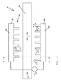
図1は、光導波路20とダイオード構造体30とを含む注入変調器10を示す。ダイオード構造体30は、正孔注入用の第1くし形構造100、図1の上部くし形構造と、電子注入用の第2くし形構造200、図1の下部くし形構造とを含む。
FIG. 1 shows an
第1くし形構造100は、くしの背骨部分120から指状に突出する、導波路20の方向に延在するpドープ半導体部分110を備える。導波路20の方向におけるpドープ半導体部分110の延伸方向は、好ましくは、くしの背骨部分120の長手方向Lからまたは導波路20の長手方向Lに対して垂直に突出する。くしの背骨部分120の長手方向Lおよび導波路20の長手方向Lは、好ましくは平行である。導波路20の長手方向Lは、その中で案内される光線の伝播方向に一致する。
The
離間した態様でおよび好ましくは互いに平行に配置されたpドープ半導体部分110は、従って、くし形構造100の歯を実例として形成し、その先端111は、ダイオード構造体30が励起されると直ちに正孔を注入するように機能する。
The p-doped
第2くし形構造200は、くしの背骨部分220の長手方向Lに対して垂直におよび導波路20の長手方向Lに対して垂直にくしの背骨部分220から突出する、導波路20の方向に延在するnドープ半導体部分210を備える。nドープ半導体部分210は離間した態様でおよび好ましくは互いに平行に配置され、ダイオード構造体30が作動する間、それらの先端211が導波路20へまたは導波路20から正孔を注入または引き抜くように機能する。
The
導波路20内で案内される光線の均一な変調を達成するために、ダイオード構造体30は、好ましくは、導波路20の共振のない部分に配置され、ここで、− 導波路の減衰は別として− 導波路20内で案内される光線Pの光線強度は少なくともほぼ一定である。
In order to achieve a uniform modulation of the light beam guided in the
導波路20内で案内される光線Pの均一な変調と同様に、図1による例示的な実施形態において、第1くし形構造100のpドープ半導体部分110が第2くし形構造200のnドープ半導体部分210に対してオフセットされることが提供される。好ましくは、このオフセットは、図1に示されるように、pドープ半導体部分110の先端111が、それぞれ場合に、nドープ半導体部分210の先端211間に存在し、およびnドープ半導体部分210の先端211が、それぞれの場合に、pドープ半導体部分110の割り当てられた先端111間に存在するように選択される。
Similar to the uniform modulation of the light beam P guided in the
第1くし形構造100のくしの背骨部分120は好ましくは、全体的にまたは少なくとも部分的に金属接触接続を提供されたpドープ半導体部分によって形成される。くしの背骨部分220は、対応して好ましくは、全体的にまたは少なくとも部分的に金属接触接続を提供されたnドープ半導体材料によって形成される。
The
図1による注入変調器10は、例えば以下のように動作可能である。
The
導波路20の領域に電荷キャリアを注入するために、順電圧が電圧または電流源Uを用いてダイオード構造体30に印加され、その結果、pドープ半導体部分110の部分において、正孔が導波路20の方向におよび第2くし形構造200の方向に放出され、nドープ半導体部分210の部分において、導波路20の方向におよびpドープ半導体部分110の方向に電子が放出される。導波路20の領域に注入された正孔および電子は導波路20内の屈折率を修正し、その結果、位相変調、および − 電荷キャリアのために − 導波路20内で案内される光線の特定の減衰が起こる。
In order to inject charge carriers into the region of the
変調の切換えをもたらすために、注入された電荷キャリアが導波路20の領域から可能な限り速く引き抜かれるように意図されている場合、逆電圧が好ましくはダイオード構造体30に印加され、その結果、導波路20の領域に位置する正孔および電子は、第1くし形構造100および第2くし形構造200によって引き抜かれる。
If the injected charge carriers are intended to be extracted from the region of the
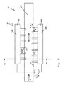
図2は、図1による注入変調器10を図1による断面線II−IIに沿った断面図で示す。
FIG. 2 shows the
導波路20は、好ましくは導波層21中に具現化された隆起した導波路であることを確認することができる。導波層21は、下部クラッディング層22上に配置され、下部クラッディング層22は垂直方向に導波するために導波層21よりも小さい屈折率を有する。
It can be ascertained that the
横方向導波のために、導波路20は、− 導波路の長手方向において見られるように − 左右において2つのウェブ部分24および25によって隣接される隆起部分23を備える。ウェブ部分24および25のウェブ高さは、隆起部分23の高さよりも小さい。
For transverse waveguiding, the
図2は、pドープ半導体部分110およびnドープ部分210の構成をさらに示す。選択された断面のために、pドープ半導体部分110のみが、示されている面内に位置し、従ってこの部分のみが実線で示されている。nドープ半導体部分210は、選択された目視方向に沿ってpドープ半導体部分110の後方に間隔をあけて配置され、従って単に点線で示されている。
FIG. 2 further illustrates the configuration of the p-doped
換言すると、図2において選択された線の種類は、pドープ半導体部分110およびnドープ半導体部分210が同じ面内に位置せず、図1に関連して既に記載したように、互いにオフセットされるという事実を図で視覚化するために使用される。
In other words, the line types selected in FIG. 2 are offset from each other, as already described in connection with FIG. 1, where the p-doped
図1および2による例示的な実施形態において、導波路20内で案内される光線の最小限の減衰に関して、2つのくし形構造100および200の構成は、pドープ半導体部分110およびnドープ半導体部分210の先端111および211がそれぞれ導波路20の隆起部分23の外側に常に存在するように選択される。
In the exemplary embodiment according to FIGS. 1 and 2, with respect to the minimum attenuation of the light guided in the
可能な限り効果的に電子および正孔を注入することに関連して、pドープ半導体部分110のドーピングおよびnドープ半導体部分210のドーピングは、導波層21の表面21aを起点にして、下部クラッディング層22まで下方に延在するような方法で選択される。このドーピング深さは、導波路20がウェブ部分24および25の全体ウェブ高さの領域において電荷キャリアで均一に満たされ得ることを保証する。
In connection with injecting electrons and holes as effectively as possible, the doping of the p-doped
図3は、構造の点で図1および2による注入変調器10に対応する注入変調器の1つの例示的な実施形態を示す。図1および2による注入変調器と対照的に、ダイオード構造体30の2つのくし形構造100および200は、導波路20のより近くに配置されている。これに関して、図3において、2つのくし形構造100および200のpドープ半導体部分110およびnドープ半導体部分210の先端111および211は、それぞれ真直ぐに導波路20内へ突出することを確認することができる。2つのくし形構造100および200のくしの背骨部分120および220のみが導波路20の外側に位置する。
FIG. 3 shows one exemplary embodiment of an injection modulator corresponding in structure to the
pドープ半導体部分110とnドープ半導体部分210との間のより短い距離のために、ダイオード構造体30の作動中、導波路20内のより高い電界強度、先に注入された電荷キャリアのより速い注入および引抜きの結果としてのより速い変調速度、および導波路20内のより高い電荷キャリア密度を達成することが可能である。欠点は、導波路20内の光線Pのより高い減衰であり、これは導波路20に突出するpドープ半導体部分110およびnドープ半導体部分210の部分によってもたらされる、すなわち、これは、2つのくし形構造100および200の歯の端部が導波路減衰を増大するためである。
Due to the shorter distance between the p-doped
減衰を最小化するために、半導体部分110および210の幅bは、半導体部分間の距離Aよりもかなり小さくなるように選択される。
In order to minimize the attenuation, the width b of the
その他の点に関して、図1および2に関連する説明は、図3による例示的な実施形態の事例に対応してあてはまる。 In other respects, the description relating to FIGS. 1 and 2 applies correspondingly to the case of the exemplary embodiment according to FIG.
図4は、図3による注入変調器10を断面線IV−IVに沿って断面で示す。pドープ半導体部分110およびnドープ半導体部分210はそれぞれウェブ部分24および25を起点にして導波路20の隆起部分23内へ真直ぐに延在することを確認することができる。それにもかかわらず、弱くドーピングされるまたはドーピングされていない中間構造部分300が、半導体部分110および210間に残り、前記中間構造部分は半導体部分を互いに分離し、光線 − 光線の少なくとも主要部分 − は、前記中間構造部分内で案内される。
FIG. 4 shows the
図4において、nドープ半導体部分210は、導波路長手方向に沿ってpドープ半導体部分110に対してオフセットされていることを同じく確認することができる。これは、図4においてnドープ半導体部分210の点線によって視覚化されている。
In FIG. 4, it can also be confirmed that the n-doped
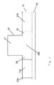
図5は、2つの干渉計アーム部分410および420を含むMZI変調器400の1つの例示的な実施形態を示す。干渉計アーム部分の一方、例えば干渉計アーム部分410は、上で図1〜4において例として説明したようなものなどの注入変調器10を備える。
FIG. 5 illustrates one exemplary embodiment of an
注入変調器10が励起されると、干渉計アーム部分410内で案内される光線の位相を、干渉計アーム部分420内で案内される光線の位相に対して変化させることが可能であり、その結果、振幅変調がMZI変調器400の出力部で起こる。
When the
図6は、MZI変調器400の1つの例示的な実施形態を示し、MZI変調器400中、両方の干渉計アーム部分410および420は、それぞれ上で図1〜4に関連して説明したようなものなどの注入変調器10を備える。
FIG. 6 shows one exemplary embodiment of an
図7は、リング変調器500の1つの例示的な実施形態を示し、リング変調器500中、導波路20はリング共振器を形成する。図1〜4に関連して説明したようなものなどの注入変調器10が、導波路20の共振器のない部分に提供される。従って、上の説明が図7による変調器10に対応して当てはまる。
FIG. 7 illustrates one exemplary embodiment of a
本発明を、好ましい例示的な実施形態を用いてより具体的に説明し詳細に記載してきたが、本発明は開示される例に限定されず、当業者は、それらの例から、本発明の保護範囲から逸脱することなく他の変形形態を導き出すことができる。 Although the present invention has been more specifically described and described in detail using preferred exemplary embodiments, the present invention is not limited to the disclosed examples, and those skilled in the art can Other variations can be derived without departing from the protection scope.
10 注入変調器
20 導波路
21 層
21a 表面
22 クラッディング層
23 隆起部分
24 ウェブ部分
25 ウェブ部分
30 ダイオード構造体
100 上部くし形構造
110 Pドープ半導体部分
111 先端
120 くしの背骨部分
200 下部くし形構造
210 Nドープ半導体部分
211 先端
220 くしの背骨部分
300 中間部分
400 MZI変調器
410 干渉計アーム部分
420 干渉計アーム部分
500 リング変調器
A 距離
b 幅
L 長手方向
P 光線
U 電圧/電流源
DESCRIPTION OF
Claims (14)
− 光導波路(20)、および、
− 少なくとも2つのpドープ半導体部分(110)と、少なくとも2つのnドープ半導体部分(210)と、前記pドープおよびnドープ半導体部分(110、210)間の少なくとも1つの弱くドーピングされたまたはドーピングされていない中間部分(300)とを含むダイオード構造体(30)
を含み、
− 前記pドープ半導体部分(110)が、− 前記導波路(20)の長手方向(L)において見たときに − 前記nドープ半導体部分(210)に対してオフセットされて配置され、および
− 前記ダイオード構造体(30)が、前記導波路(20)の共振のない部分に配置され、ここで、− 導波路減衰は別として −前記導波路(20)内で案内される前記光線(P)の光線強度が一定である、注入変調器(10)において、
− 前記pドープ半導体部分(110)が、− 前記導波路(20)の前記長手方向(L)において見たときに、かつ導波路中心に対して − 前記導波路(20)の一方の側に存在し、前記nドープ半導体部分(210)が前記導波路(20)の他方の側に存在し、かつ前記中間部分(300)が前記導波路中心の領域に存在し、
− 前記半導体部分(110、210)が、前記導波路長手方向(L)に対して横方向に、前記導波路(20)の前記導波路中心の方向に延在し、
− 前記pドープ半導体部分(110)が、− 前記導波路(20)の前記長手方向(L)において見たときに − 前記nドープ半導体部分(210)との重なりがなく、
− 前記導波路(20)が、導波する持ち上がった隆起部分(23)と、隆起部長手方向において見たときに前記隆起部分(23)と平行に延びる2つの隣接するウェブ部分(24、25)とを含む隆起導波路であり、
− 前記pドープ半導体部分(110)が、前記2つのウェブ部分(24、25)の一方に配置され、
− 前記nドープ半導体部分(210)が、前記2つのウェブ部分(24、25)の他方に配置され、
− 前記半導体部分(110、210)が、前記2つのウェブ部分(24、25)を起点にして前記導波路(20)の前記隆起部分(23)内へ延在することを特徴とする注入変調器(10)。 In an injection modulator (10) for modulating the light beam (P):
-An optical waveguide (20), and
At least two p-doped semiconductor parts (110), at least two n-doped semiconductor parts (210) and at least one weakly doped or doped between said p-doped and n-doped semiconductor parts (110, 210); Diode structure (30) including a non-intermediate portion (300)
Including
The p-doped semiconductor portion (110) is arranged offset with respect to the n-doped semiconductor portion (210) when viewed in the longitudinal direction (L) of the waveguide (20), and A diode structure (30) is arranged in a non-resonant part of the waveguide (20), where:-apart from waveguide attenuation-the light beam (P) guided in the waveguide (20) In the injection modulator (10) where the light intensity of
-When the p-doped semiconductor portion (110) is seen in the longitudinal direction (L) of the waveguide (20) and with respect to the center of the waveguide-on one side of the waveguide (20) Present, the n-doped semiconductor portion (210) is on the other side of the waveguide (20), and the intermediate portion (300) is in a region in the center of the waveguide,
- wherein the semiconductor portion (110, 210) is pre-transversely to Kishirube waveguide longitudinal direction (L), extend in the direction of the waveguide center of the waveguide (20),
- wherein p-doped semiconductor portion (110) - said waveguide when viewed in the longitudinal direction of the (20) (L) - overlap rather name of the previous SL n-doped semiconductor portion (210),
A raised ridge (23) in which the waveguide (20) guides and two adjacent web portions (24, 25) extending parallel to the ridge (23) when viewed in the longitudinal direction of the ridge ) And a raised waveguide including
The p-doped semiconductor portion (110) is disposed on one of the two web portions (24, 25);
The n-doped semiconductor part (210) is arranged on the other of the two web parts (24, 25);
An injection modulation characterized in that the semiconductor part (110, 210) extends into the raised part (23) of the waveguide (20) starting from the two web parts (24, 25); Vessel (10).
− 前記隆起部分の少なくとも中心に前記pおよびnドープ半導体部分(110、210)がないことを特徴とする注入変調器(10)。 Injection modulator according to claim 1 (10) Te odor,
- injection modulator, wherein the absence p and n-doped semiconductor portion (110, 210) to at least the center of the front Symbol raised portion (10).
− 前記pドープ半導体部分(110)が、pドープくし形構造(100)の歯部分を形成し、その歯は前記導波路長手方向(L)において互いに距離を置いて配置され、かつ、前記導波路(20)の外側に配置された共通の接触接続部を起点にして、前記導波路長手方向(L)に対して横方向に外側から、前記導波路(20)の前記導波路中心の前記方向に延在し、およびThe p-doped semiconductor portion (110) forms a tooth portion of a p-doped comb structure (100), the teeth being spaced apart from each other in the longitudinal direction of the waveguide (L), and Starting from the common contact connection portion arranged outside the waveguide (20), the waveguide center of the waveguide (20) from the outside in the lateral direction with respect to the waveguide longitudinal direction (L). Extending in the direction, and
− 前記nドープ半導体部分(210)が、nドープくし形構造(200)の歯部分を形成し、その歯は前記導波路長手方向(L)において互いに距離を置いて配置され、かつ前記導波路(20)の外側に配置された共通の接触接続部を起点にして、前記導波路長手方向(L)に対して横方向に外側から、前記導波路(20)の前記導波路中心の前記方向に延在することを特徴とする注入変調器(10)。The n-doped semiconductor portion (210) forms a tooth portion of an n-doped comb structure (200), the teeth being spaced apart from each other in the waveguide longitudinal direction (L), and the waveguide The direction of the waveguide center of the waveguide (20) from the outside in the lateral direction with respect to the longitudinal direction (L) of the waveguide, starting from the common contact connection portion arranged outside (20) An injection modulator (10), characterized in that it extends into
− 前記隆起導波路が、導波層(21)と、下にある下部クラッディング層(22)とを含み、およびThe raised waveguide comprises a waveguiding layer (21) and an underlying lower cladding layer (22); and
− 前記nドープ半導体部分(210)のドーピングおよび前記pドープ半導体部分(110)のドーピングが、前記隆起導波路の前記導波層(21)の表面(21a)から前記下部クラッディング層(22)まで延在することを特徴とする注入変調器(10)。The doping of the n-doped semiconductor part (210) and the doping of the p-doped semiconductor part (110) from the surface (21a) of the waveguide layer (21) of the raised waveguide to the lower cladding layer (22) Injection modulator (10) characterized in that it extends to
− 前記pドープ半導体部分(110)の幅(b)が、隣接するpドープ半導体部分(110)間の距離(A)よりも小さく、およびThe width (b) of the p-doped semiconductor portion (110) is smaller than the distance (A) between adjacent p-doped semiconductor portions (110); and
− 前記nドープ半導体部分(210)の幅(b)が、隣接するnドープ半導体部分(210)間の距離(A)よりも小さいことを特徴とする注入変調器(10)。An injection modulator (10) characterized in that the width (b) of the n-doped semiconductor part (210) is smaller than the distance (A) between adjacent n-doped semiconductor parts (210).
− 前記pドープ半導体部分(110)が、第1くし形構造(100)の構成要素を形成し、The p-doped semiconductor portion (110) forms a component of the first comb structure (100);
− 前記nドープ半導体部分(210)が第2くし形構造(200)の構成要素を形成し、およびThe n-doped semiconductor portion (210) forms a component of a second comb structure (200); and
− 前記2つのくし形構造(100、200)のくしの背骨部分(120、220)が、前記導波路(20)と平行に整列され、かつ前記隆起導波路の前記持ち上がった隆起部分(23)から距離を置いて存在することを特徴とする注入変調器(10)。The comb backbone (120, 220) of the two comb structures (100, 200) is aligned parallel to the waveguide (20) and the raised raised portion (23) of the raised waveguide; Injection modulator (10) characterized in that it exists at a distance from
− 前記pドープ半導体部分(110)の少なくとも1つが、− 前記導波路(20)の前記長手方向(L)において見たときに − 斜め反対側に存在する2つのnドープ半導体部分(210)間の中心に配置され、および-At least one of the p-doped semiconductor portions (110)-when viewed in the longitudinal direction (L) of the waveguide (20)-between two n-doped semiconductor portions (210) present diagonally opposite sides Placed in the center of, and
− 前記nドープ半導体部分(210)の少なくとも1つが、− 前記導波路(20)の前記長手方向(L)において見たときに − 斜め反対側に存在する2つのpドープ半導体部分(110)間の中心に配置されることを特徴とする注入変調器(10)。-At least one of the n-doped semiconductor portions (210)-when viewed in the longitudinal direction (L) of the waveguide (20)-between two p-doped semiconductor portions (110) existing diagonally opposite sides Injection modulator (10), characterized in that it is arranged in the center of
− 前記pドープ半導体部分(110)が、pドープくし形構造(100)またはその構成要素を形成し、かつ前記nドープ半導体部分(210)が、nドープくし形構造(200)またはその構成要素を形成し、The p-doped semiconductor portion (110) forms a p-doped comb structure (100) or a component thereof, and the n-doped semiconductor portion (210) comprises an n-doped comb structure (200) or a component thereof. Form the
− 前記pドープくし形構造(100)が、前記導波路(20)の一方の側に配置され、かつ前記nドープくし形構造(200)が、前記導波路(20)の他方の側に配置され、およびThe p-doped comb structure (100) is arranged on one side of the waveguide (20) and the n-doped comb structure (200) is arranged on the other side of the waveguide (20) And
− 前記2つのくし形構造の歯が、前記導波路(20)の前記導波路中心の前記方向において整列されることを特徴とする注入変調器(10)。An injection modulator (10), characterized in that the teeth of the two comb structures are aligned in the direction of the waveguide center of the waveguide (20).
− 前記導波路(20)がMZI変調器(400)を形成し、およびThe waveguide (20) forms an MZI modulator (400); and
− 前記MZI変調器のアーム部分の少なくとも1つが、電荷キャリアを注入するためのダイオード構造体(30)を備えることを特徴とする注入変調器(10)。An injection modulator (10), characterized in that at least one of the arm parts of the MZI modulator comprises a diode structure (30) for injecting charge carriers;
− 少なくとも2つのpドープ半導体部分(110)と、少なくとも2つのnドープ半導体部分(210)と、前記pドープおよびnドープ半導体部分(110、210)間の少なくとも1つの弱くドーピングされたまたはドーピングされていない中間部分(300)とを含むダイオード構造体(30)を用いて、正孔の注入または引抜きが前記導波路(20)の一方の側から実行され、かつ電子の注入または引抜きが前記導波路(20)の他方の側から実行され、At least two p-doped semiconductor parts (110), at least two n-doped semiconductor parts (210) and at least one weakly doped or doped between said p-doped and n-doped semiconductor parts (110, 210); Using a diode structure (30) that includes a non-intermediate portion (300), hole injection or extraction is performed from one side of the waveguide (20), and electron injection or extraction is performed in the conductive structure. Performed from the other side of the waveguide (20),
− 前記pドープ半導体部分(110)が、− 導波路長手方向(L)において見たときに、かつ導波路中心に対して − 前記導波路(20)の一方の側に存在し、前記nドープ半導体部分(210)が前記導波路(20)の他方の側に存在し、かつ前記中間部分(300)が前記導波路中心の領域に存在し、The p-doped semiconductor portion (110) is present in one side of the waveguide (20) when viewed in the longitudinal direction (L) of the waveguide and with respect to the center of the waveguide; A semiconductor portion (210) is present on the other side of the waveguide (20), and the intermediate portion (300) is present in the central region of the waveguide;
− 前記半導体部分(110、210)が、前記導波路長手方向(L)に対して横方向に、前記導波路(20)の前記導波路中心の方向に延在し、The semiconductor portion (110, 210) extends in a direction transverse to the waveguide longitudinal direction (L), in the direction of the waveguide center of the waveguide (20);
− 前記pドープ半導体部分(110)が、− 前記導波路(20)の前記長手方向(L)において見たときに − 前記nドープ半導体部分(210)に対してオフセットされ、かつ前記nドープ半導体部分(210)に対して重なりがなく、The p-doped semiconductor portion (110) is offset with respect to the n-doped semiconductor portion (210) when viewed in the longitudinal direction (L) of the waveguide (20) and the n-doped semiconductor There is no overlap with part (210),
− 前記導波路(20)が、導波する持ち上がった隆起部分(23)と、隆起部長手方向において見たときに前記隆起部分(23)と平行に延びる2つの隣接するウェブ部分(24、25)とを含む隆起導波路であり、The waveguide (20) is a raised raised section (23) that guides and two adjacent web sections (24, 25) that run parallel to the raised section (23) when viewed in the longitudinal direction of the ridge; ) And a raised waveguide including
− 前記pドープ半導体部分(110)が、前記2つのウェブ部分(24、25)の一方に配置され、The p-doped semiconductor portion (110) is disposed on one of the two web portions (24, 25);
− 前記nドープ半導体部分(210)が、前記2つのウェブ部分(24、25)の他方に配置され、The n-doped semiconductor part (210) is arranged on the other of the two web parts (24, 25);
− 前記半導体部分(110、210)が、前記2つのウェブ部分(24、25)を起点にして前記導波路(20)の前記隆起部分(23)内へ延在することを特徴とする方法。The semiconductor part (110, 210) extends into the raised part (23) of the waveguide (20) starting from the two web parts (24, 25);
Applications Claiming Priority (3)
| Application Number | Priority Date | Filing Date | Title |
|---|---|---|---|
| DE102014219295.1A DE102014219295A1 (en) | 2014-09-24 | 2014-09-24 | injection modulator |
| DE102014219295.1 | 2014-09-24 | ||
| PCT/DE2015/200460 WO2016045675A1 (en) | 2014-09-24 | 2015-09-21 | Injection modulator |
Publications (2)
| Publication Number | Publication Date |
|---|---|
| JP2017529569A JP2017529569A (en) | 2017-10-05 |
| JP6599981B2 true JP6599981B2 (en) | 2019-10-30 |
Family
ID=54697420
Family Applications (1)
| Application Number | Title | Priority Date | Filing Date |
|---|---|---|---|
| JP2017516784A Active JP6599981B2 (en) | 2014-09-24 | 2015-09-21 | Injection modulator |
Country Status (7)
| Country | Link |
|---|---|
| US (1) | US9817295B2 (en) |
| EP (1) | EP3198750B1 (en) |
| JP (1) | JP6599981B2 (en) |
| CN (1) | CN106716239B (en) |
| CA (1) | CA2961685C (en) |
| DE (1) | DE102014219295A1 (en) |
| WO (1) | WO2016045675A1 (en) |
Families Citing this family (3)
| Publication number | Priority date | Publication date | Assignee | Title |
|---|---|---|---|---|
| WO2018045300A1 (en) * | 2016-09-01 | 2018-03-08 | Luxtera, Inc. | Method and system for a vertical junction high-speed phase modulator |
| CN107238951B (en) * | 2017-07-05 | 2023-10-27 | 浙江大学 | Low bias large bandwidth electro-optic modulator |
| EP3667279B1 (en) * | 2018-12-10 | 2021-12-01 | FRAUNHOFER-GESELLSCHAFT zur Förderung der angewandten Forschung e.V. | Sensing device |
Family Cites Families (10)
| Publication number | Priority date | Publication date | Assignee | Title |
|---|---|---|---|---|
| WO2002069004A2 (en) * | 2001-02-22 | 2002-09-06 | Bookham Technology Plc | Semiconductor optical waveguide device |
| US7880201B2 (en) * | 2006-11-09 | 2011-02-01 | International Business Machines Corporation | Optical modulator using a serpentine dielectric layer between silicon layers |
| KR101768676B1 (en) * | 2010-10-22 | 2017-08-16 | 삼성전자주식회사 | Silicon phase shifter, electro-optic modulator and photonic integrated circuit employing the same |
| DE102011005422B4 (en) | 2011-03-11 | 2013-01-31 | Ihp Gmbh - Innovations For High Performance Microelectronics / Leibniz-Institut Für Innovative Mikroelektronik | Electro-optical modulator |
| CN102495449B (en) * | 2011-12-07 | 2013-09-11 | 中国科学院半导体研究所 | Induced waveguide grating of tunable current carrier |
| SG2013082102A (en) * | 2012-11-05 | 2014-06-27 | Agency Science Tech & Res | Method for forming an optical modulator |
| JP6020096B2 (en) * | 2012-11-30 | 2016-11-02 | 富士通株式会社 | Optical modulator and optical transmitter |
| FR3009893B1 (en) * | 2013-08-26 | 2016-12-30 | Commissariat Energie Atomique | METHOD FOR MANUFACTURING AN AREA PIN CORRUGATED AND SPACED DOPED ZONES, APPLICATION TO THE MANUFACTURE OF ELECTRO-OPTICAL SILICON MODULATORS AND GERMANIUM PHOTO-DETECTORS |
| JP6303718B2 (en) * | 2014-03-28 | 2018-04-04 | 富士通株式会社 | Optical semiconductor device and manufacturing method thereof |
| US9575338B2 (en) * | 2015-03-10 | 2017-02-21 | International Business Machines Corporation | Controlled-capacitance full-depletion interdigitated pin modulator |
-
2014
- 2014-09-24 DE DE102014219295.1A patent/DE102014219295A1/en not_active Withdrawn
-
2015
- 2015-09-21 CN CN201580049944.0A patent/CN106716239B/en active Active
- 2015-09-21 CA CA2961685A patent/CA2961685C/en active Active
- 2015-09-21 JP JP2017516784A patent/JP6599981B2/en active Active
- 2015-09-21 US US15/512,873 patent/US9817295B2/en active Active
- 2015-09-21 WO PCT/DE2015/200460 patent/WO2016045675A1/en active Application Filing
- 2015-09-21 EP EP15798323.0A patent/EP3198750B1/en active Active
Also Published As
| Publication number | Publication date |
|---|---|
| CA2961685C (en) | 2023-03-28 |
| US20170299939A1 (en) | 2017-10-19 |
| CA2961685A1 (en) | 2016-03-31 |
| WO2016045675A1 (en) | 2016-03-31 |
| US9817295B2 (en) | 2017-11-14 |
| CN106716239B (en) | 2018-04-10 |
| CN106716239A (en) | 2017-05-24 |
| EP3198750A1 (en) | 2017-08-02 |
| EP3198750B1 (en) | 2018-11-28 |
| DE102014219295A1 (en) | 2016-03-24 |
| JP2017529569A (en) | 2017-10-05 |
Similar Documents
| Publication | Publication Date | Title |
|---|---|---|
| US9235101B2 (en) | Optical source | |
| US20140241656A1 (en) | Electro-Optic Modulator | |
| US7113329B2 (en) | Optical logical circuits based on lasing semiconductor optical amplifiers | |
| JP6599981B2 (en) | Injection modulator | |
| JP2009282460A (en) | Optical modulator | |
| US20200409187A1 (en) | Optical phase modulator and optical modulator | |
| CN104937791A (en) | Laser device, optical modulation device, and optical semiconductor element | |
| US6912079B2 (en) | Method and apparatus for phase shifting an optical beam in an optical device | |
| JP2012078508A (en) | Optical waveguide device | |
| JP3839710B2 (en) | Semiconductor optical modulator, Mach-Zehnder optical modulator, and optical modulator integrated semiconductor laser | |
| Pathak | Photonics integrated circuits | |
| JP5858476B2 (en) | Optical element | |
| US9281661B2 (en) | Integrated optoelectronic device comprising a Mach-Zehnder modulator and a vertical cavity surface emitting laser (VCSEL) | |
| JP4863272B2 (en) | Optical flip-flop | |
| JP4141451B2 (en) | Semiconductor optical modulator | |
| JP5945240B2 (en) | Optical phase modulator | |
| Zhang et al. | Silicon microring-based signal modulation for chip-scale optical interconnection | |
| JP6353474B2 (en) | Light modulator | |
| JP2016114712A (en) | Semiconductor Mach-Zehnder optical modulator | |
| JP6151958B2 (en) | Light modulation element and method for driving light modulation element | |
| May-Arrioja et al. | Ultra-compact multimode interference InGaAsP multiple quantum well modulator | |
| JP5918787B2 (en) | Wavelength multiplexing transmitter | |
| Rabus et al. | Devices | |
| JP2809216B2 (en) | Nonlinear optical waveguide | |
| Pérez-Galacho et al. | 25 Gbit/s O-Band push-pull Mach-Zehnder silicon modulator for datacom applications |
Legal Events
| Date | Code | Title | Description |
|---|---|---|---|
| A621 | Written request for application examination |
Free format text: JAPANESE INTERMEDIATE CODE: A621 Effective date: 20180920 |
|
| A871 | Explanation of circumstances concerning accelerated examination |
Free format text: JAPANESE INTERMEDIATE CODE: A871 Effective date: 20180920 |
|
| A977 | Report on retrieval |
Free format text: JAPANESE INTERMEDIATE CODE: A971007 Effective date: 20190118 |
|
| A975 | Report on accelerated examination |
Free format text: JAPANESE INTERMEDIATE CODE: A971005 Effective date: 20190221 |
|
| A131 | Notification of reasons for refusal |
Free format text: JAPANESE INTERMEDIATE CODE: A131 Effective date: 20190305 |
|
| A601 | Written request for extension of time |
Free format text: JAPANESE INTERMEDIATE CODE: A601 Effective date: 20190603 |
|
| A521 | Request for written amendment filed |
Free format text: JAPANESE INTERMEDIATE CODE: A523 Effective date: 20190802 |
|
| TRDD | Decision of grant or rejection written | ||
| A01 | Written decision to grant a patent or to grant a registration (utility model) |
Free format text: JAPANESE INTERMEDIATE CODE: A01 Effective date: 20190910 |
|
| A61 | First payment of annual fees (during grant procedure) |
Free format text: JAPANESE INTERMEDIATE CODE: A61 Effective date: 20191003 |
|
| R150 | Certificate of patent or registration of utility model |
Ref document number: 6599981 Country of ref document: JP Free format text: JAPANESE INTERMEDIATE CODE: R150 |
|
| S111 | Request for change of ownership or part of ownership |
Free format text: JAPANESE INTERMEDIATE CODE: R313117 |
|
| R350 | Written notification of registration of transfer |
Free format text: JAPANESE INTERMEDIATE CODE: R350 |
|
| R250 | Receipt of annual fees |
Free format text: JAPANESE INTERMEDIATE CODE: R250 |
|
| R250 | Receipt of annual fees |
Free format text: JAPANESE INTERMEDIATE CODE: R250 |