JP6591908B2 - Radiation detector - Google Patents
Radiation detector Download PDFInfo
- Publication number
- JP6591908B2 JP6591908B2 JP2016029218A JP2016029218A JP6591908B2 JP 6591908 B2 JP6591908 B2 JP 6591908B2 JP 2016029218 A JP2016029218 A JP 2016029218A JP 2016029218 A JP2016029218 A JP 2016029218A JP 6591908 B2 JP6591908 B2 JP 6591908B2
- Authority
- JP
- Japan
- Prior art keywords
- radiation
- detection
- detector
- radiation detection
- stacked
- Prior art date
- Legal status (The legal status is an assumption and is not a legal conclusion. Google has not performed a legal analysis and makes no representation as to the accuracy of the status listed.)
- Expired - Fee Related
Links
Images


Landscapes
- Measurement Of Radiation (AREA)
Description
本発明は、種々の構造物の非破壊検査等に用いられる放射線検出装置に関する。 The present invention relates to a radiation detection apparatus used for nondestructive inspection of various structures.
従来より、X線やγ線等の放射線を用いた非破壊検査装置が知られている。これらの放射線を検出する装置としては、例えば特許文献1に開示された装置がある。特許文献1の装置に設けられたX線検出要素は、公知のシリコンストリップ検出器(SSD)と同様に製造されるX線検出半導体と、金属板からなるX線阻止部材とを交互に重ねて構成される。X線阻止部材は、X線の入射方向側においてX線検出半導体より突出して形成されている。特許文献1では、かかるX線阻止部材の突出によってコリメータ機能を有するようになり、被検体内で散乱された散乱X線のX線検出半導体への入射が阻止されるようになる。つまり、特許文献1の検出装置は、X線阻止部材によってコリメータを一体に備えた構成となる。 Conventionally, non-destructive inspection apparatuses using radiation such as X-rays and γ-rays are known. As an apparatus for detecting these radiations, there is an apparatus disclosed in Patent Document 1, for example. The X-ray detection element provided in the apparatus of Patent Document 1 is formed by alternately stacking an X-ray detection semiconductor manufactured in the same manner as a known silicon strip detector (SSD) and an X-ray blocking member made of a metal plate. Composed. The X-ray blocking member is formed so as to protrude from the X-ray detection semiconductor on the X-ray incident direction side. In Patent Document 1, the projection of the X-ray blocking member has a collimator function, and the scattered X-rays scattered in the subject are prevented from entering the X-ray detection semiconductor. That is, the detection apparatus of Patent Document 1 has a configuration in which a collimator is integrally provided by an X-ray blocking member.
しかしながら、特許文献1のようにコリメータを備えた構成とすると、コリメータの影による不感領域が発生するため、高い位置分解能を達成することが難しくなる、という問題がある。また、X線検出半導体の間にX線阻止部材が積層されるので、当該X線阻止部材の厚み分、X線検出半導体同士が積層方向に離れてしまい、これによっても、高い位置分解能を達成することが難しくなる、という問題がある。 However, when a configuration including a collimator as in Patent Document 1 is used, there is a problem in that it is difficult to achieve a high position resolution because a dead area due to the shadow of the collimator is generated. Further, since the X-ray blocking member is stacked between the X-ray detecting semiconductors, the X-ray detecting semiconductors are separated from each other in the stacking direction by the thickness of the X-ray blocking member, thereby achieving high position resolution. There is a problem that it becomes difficult to do.
本発明は、かかる点に鑑みてなされたものであり、放射線検出の高分解能化を図ることができる放射線検出装置を提供することを目的とする。 This invention is made | formed in view of this point, and it aims at providing the radiation detection apparatus which can aim at the high resolution of a radiation detection.
本発明の放射線検出装置は、厚み方向に積層されて一端面を放射線の入射面として放射線を検出する複数枚の放射線検出体と、前記放射線検出体が検出した放射線のパルス信号を処理する信号処理部及び当該信号処理部が実装される主基板を有する実装体とを備え、前記放射線検出体の前記入射面側にコリメータを設けない放射線検出装置であって、前記放射線検出体は、検出体用基板と、当該検出体用基板の面内に実装される半導体素子と、当該半導体素子の一方の主面に一軸方向に並列して配列され長手方向が前記入射面に直交する複数の短冊状のストリップ電極とを備え、前記信号処理部は、前記放射線検出体の検出信号に応じ、被検体での散乱放射線のパルス信号と、透過放射線のパルス信号とを弁別する弁別部と、前記弁別部で弁別された透過放射線のパルス信号を計数する演算部とを備え、前記実装体の枚数は、前記放射線検出体の枚数より少ないことを特徴とする。 The radiation detection apparatus of the present invention includes a plurality of radiation detectors that are stacked in the thickness direction and detect radiation using one end surface as a radiation incident surface, and signal processing that processes a pulse signal of radiation detected by the radiation detector And a mounting body having a main substrate on which the signal processing section is mounted, and a radiation detection apparatus that does not provide a collimator on the incident surface side of the radiation detection body, the radiation detection body for the detection body A substrate, a semiconductor element mounted in a plane of the detector substrate, and a plurality of strip-like elements arranged in parallel in a uniaxial direction on one main surface of the semiconductor element and having a longitudinal direction orthogonal to the incident surface. A strip electrode, and the signal processing unit is configured to discriminate a pulse signal of scattered radiation from a subject and a pulse signal of transmitted radiation according to a detection signal of the radiation detector, and a discrimination unit valve And a calculator for counting a pulse signal of the transmitted radiation that is, the number of the mounting body, characterized in that less than the number of the radiation detector.
この構成によれば、透過放射線のパルス信号を弁別及び計数するので、コリメータを設けずに放射線を検出でき、不感領域の発生を抑制して高い位置分解能を達成することができる。また、上述した従来構造のX線阻止部材をなくすことができるので、放射線検出体の積層方向の間隔を小さくでき、これによっても、高い位置分解能を実現することができる。しかも、放射線検出体の枚数より実装体の枚数の方が少ないので、実装体における信号処理部の厚みの制約を緩和して放射線検出体の積層方向の間隔を短くでき、位置分解能を高くすることができる。 According to this configuration, since the pulse signal of the transmitted radiation is discriminated and counted, the radiation can be detected without providing a collimator, and the generation of the insensitive area can be suppressed and high position resolution can be achieved. Moreover, since the X-ray blocking member having the conventional structure described above can be eliminated, the interval in the stacking direction of the radiation detectors can be reduced, and this also realizes high position resolution. In addition, since the number of mounted bodies is smaller than the number of radiation detectors, it is possible to relax the restrictions on the thickness of the signal processing unit in the mounted body, shorten the interval in the stacking direction of the radiation detectors, and increase the position resolution. Can do.
本発明によれば、被検体での透過放射線のパルス信号を弁別及び計数し、また、放射線検出体より実装体の枚数が少なくなるので、放射線検出の高分解能化を図ることができる。 According to the present invention, the pulse signal of the transmitted radiation in the subject is discriminated and counted, and the number of mounted bodies is smaller than that of the radiation detector, so that the resolution of radiation detection can be increased.
以下に、本発明の実施の形態について、添付図面を参照して詳細に説明する。なお、本発明は、下記の実施の形態に限定されるものではなく、その要旨を変更しない範囲内で適宜変形して実施することができるものである。以下の図においては、説明の便宜上、一部の構成を省略することがある。また、以下の説明において、特に明示しない限り、「上」、「下」、「左」、「右」、「前」、「後」は、各図において矢印で示した方向を基準として用いる。但し、以下の各実施の形態での各構成の向きは、一例にすぎず、任意の向きに変更することができる。 Hereinafter, embodiments of the present invention will be described in detail with reference to the accompanying drawings. In addition, this invention is not limited to the following embodiment, It can deform | transform suitably and implement in the range which does not change the summary. In the following drawings, some components may be omitted for convenience of explanation. In the following description, unless otherwise specified, “upper”, “lower”, “left”, “right”, “front”, and “rear” are used with reference to directions indicated by arrows in the drawings. However, the direction of each component in each of the following embodiments is merely an example, and can be changed to an arbitrary direction.
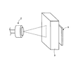
以下の実施の形態では、放射線検出装置としてX線検出装置を採用した場合を説明するが、放射線検出装置としては、α線やβ線、中性子線等の粒子放射線や、X線と同様に電磁放射線となるγ線を検出する装置を採用することができる。図1は、実施の形態に係る放射線検出装置の使用例を示す概略図である。図1に示すように、実施の形態に係る放射線検出装置1は、例えば、橋梁や原子炉周辺の構造物等の大型構造物の健全性等を評価するための非破壊検査に用いられる。非破壊検査では、線源となる線形加速器(ライナック)2を用いて生成された高エネルギーX線を被検体(構造物)3に照射し、被検体3を透過したX線を放射線検出装置1で検出することが例示できる。
In the following embodiment, a case where an X-ray detection device is adopted as a radiation detection device will be described. However, as a radiation detection device, particle radiation such as α-rays, β-rays, neutrons, etc. An apparatus for detecting γ-rays that become radiation can be employed. FIG. 1 is a schematic diagram illustrating a usage example of the radiation detection apparatus according to the embodiment. As shown in FIG. 1, the radiation detection apparatus 1 according to the embodiment is used for a nondestructive inspection for evaluating the soundness and the like of a large structure such as a bridge or a structure around a nuclear reactor, for example. In the non-destructive inspection, the subject (structure) 3 is irradiated with high energy X-rays generated using a linear accelerator (linac) 2 serving as a radiation source, and the X-ray transmitted through the
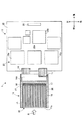
図2は、実施の形態に係る放射線検出装置の内部構造の平面図である。図3は、実施の形態に係る放射線検出装置の内部構造の縦断面図である。図2及び図3に示すように、放射線検出装置1は、複数枚(本実施の形態では5枚)の放射線検出体としてのシリコンストリップ検出器11に対し、1枚の実装体12が設けられ、それらは図示省略した筐体内に組み込まれる。複数枚のシリコンストリップ検出器11は、上下方向(厚み方向)に積層され、前端面を放射線の入射面11aとして前方から入射されるX線(放射線)Rを検出する。
FIG. 2 is a plan view of the internal structure of the radiation detection apparatus according to the embodiment. FIG. 3 is a longitudinal sectional view of the internal structure of the radiation detection apparatus according to the embodiment. As shown in FIGS. 2 and 3, the radiation detection apparatus 1 is provided with a
シリコンストリップ検出器11は、検出体用基板としてのプリント基板14と、プリント基板14の面内前方領域に実装される薄板状の半導体素子15と、半導体素子の上面(一方の主面)に設けられる複数のストリップ電極16(図3では不図示)とを備えている。半導体素子15の構成については後述する。複数のストリップ電極16は、それぞれ長手方向が入射面11aに直交する(前後方向に延びる)短冊状に形成されるとともに、左右方向(一軸方向)に並列して配列されている。ストリップ電極16は、プリント基板14に対し、ワイヤボンディングによってワイヤ17で1本ずつ接続されており、ストリップ電極16からのパルス信号をそれぞれ独立したチャネルにて検出できるようになっている。ワイヤ17は、ストリップ電極16の上面から膨らむように湾曲して形成される。なお、検出体用基板としてプリント基板14を用いたが、これに代えてFPC(Flexible Printed Circuits)を用いてもよい。
The
プリント基板14の上面における半導体素子15の設置領域は、その隣接領域に対して一段低くなるように凹んで形成されている。この凹んだ領域に半導体素子15が設置されるので、プリント基板14の下面から半導体素子15の上面までの高さを低くすることができる。プリント基板14における半導体素子15の後方において、符号14Aで示す領域は、CR回路等の図示省略した各種電子部品が実装される実装領域14Aとされる。この実装領域14Aにて、ストリップ電極16から出力されたパルス信号がI/V変換され、フレキシブルケーブル18を介して実装体12側に送信される。帯状となるフレキシブルケーブル18は、複数のシリコンストリップ検出器11に応じて1本ずつ設けられて実装体12の所定部分に接続される。
The installation region of the
複数のシリコンストリップ検出器11におけるそれぞれのプリント基板14の上面には、図2及び図3において網点で示すスペーサ20が設けられている。スペーサ20は、上面視でプリント基板14の左右両端に沿う位置と、半導体素子15及び実装領域14Aの境界位置とに設けられる。スペーサ20の上面には、シリコンストリップ検出器11の積層によって上方に隣り合う他のプリント基板14の下面が接触される。従って、スペーサ20は、プリント基板14の上下方向(厚さ方向)に隣り合う他のプリント基板14との間の間隔を確保する。スペーサ20の厚み(高さ)は、湾曲するワイヤ17に対し上方のプリント基板14の下面が非接触となるように設定され、これにより、上方のプリント基板14からワイヤ17に力が加わることが回避される。
実装体12は、プリント基板からなる主基板22と、主基板22の上下両面に実装された回路となる信号処理部23とを備えている。信号処理部23は、ストリップ電極16が検出したパルス信号を入力して処理するASIC23a(Application Specific Integrated Circuit)や、FPGA23b(Field-Programmable Gate Array)等を含み、その処理については後述する。本実施の形態の信号処理部23では、シリコンストリップ検出器11の設置数に応じてASIC23aも複数(本実施の形態では5体)設けられている。また、実装体12の上下各面には、ASIC23a及びFPGA23bの他に、図2中方形状に簡素化して示したICや記憶装置等の各種電子部品が実装され、また、実装体12の後端側には信号を入出力するためのコネクタ25が設けられている。
The
本実施の形態では、シリコンストリップ検出器11が5枚に対し、実装体12が1枚設けられ、実装体12の枚数はシリコンストリップ検出器11の枚数より少なくなっている。そして、5枚積層されたシリコンストリップ検出器11の全体厚みより、各種電子部品等を含む実装体12の上下幅の方が小さく形成され、積層されたシリコンストリップ検出器11の高さに収まるよう、その後方に実装体12が配置される。従って、積層されたシリコンストリップ検出器11をX線(放射線)Rの入射側つまり前側から見たときに、高さ方向において、積層されたシリコンストリップ検出器11に実装体12が重なって隠れるように設けられる。これにより、積層されたシリコンストリップ検出器11がX線Rの遮蔽体となって実装体12を保護することができ、実装体12に実装される各部品に対する耐放射線性の向上を図ることができる。
In the present embodiment, one mounting
なお、本実施の形態では、X線(放射線)Rの入射側つまり前側から見たときに、左右方向において、積層されたシリコンストリップ検出器11に実装体12の左右が重なって隠れるようになっていないが、これに重なって隠れるようにしてもよい。これにより、積層されたシリコンストリップ検出器11がX線Rの遮蔽体となって実装体12を保護することができ、実装体12に実装される各部品に対する耐放射線性の向上を図ることができる。
In the present embodiment, when viewed from the X-ray (radiation) R incident side, that is, the front side, the left and right sides of the mounting
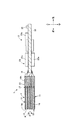
続いて、シリコンストリップ検出器11における半導体素子15及びストリップ電極16の構成について図4を参照して説明する。図4は、実施の形態に係るシリコンストリップ検出器を断面視した説明用模式図である。図4に示すように、半導体素子15は、基材となるP型のシリコン基板31の上面(一方の面)に、N型のアモルファスシリコン膜32を形成して構成される。
Next, the configuration of the
アモルファスシリコン膜32の形成は、CVD(Chemical Vapor Deposition)装置にて所定厚み製膜することが例示できる。アモルファスシリコン膜32の上面には、アルミ蒸着等によって複数のストリップ電極16が配列され、シリコン基板31における下面(他方の面)の概略全領域には、裏面電極34が形成されている。ストリップ電極16及び裏面電極34に逆方向バイアスの電圧を印加すると、シリコン基板31とアモルファスシリコン膜32との間に空乏層が形成される。この空乏層にX線が入射されると、空乏層内でのX線の相互作用により、逆バイアスされている電場にて電子は+方向へ、正孔は−方向へ移動する。この電子及び正孔の流れが電流となり、かかる電流がパルス信号としてストリップ電極16から出力される。なお、半導体素子15は、インプラによるPN接合やPIN構造の半導体シリコン素子としてもよい。
The formation of the
パルス信号を出力するストリップ電極16は、空乏層でのX線の反応位置に最も近いストリップ電極16となる。従って、ストリップ電極16の形成領域がX線に対する有感領域となり、パルス信号を出力したストリップ電極16はX線の入射位置を表すことになる。これにより、1体の半導体素子15において、ストリップ電極16の配列方向(左右方向)での形成間隔で、X線の入射位置の情報が得られる位置分解能を有する。
The
シリコンストリップ検出器11は、上下方向に複数枚積層されるので、半導体素子15も上下に複数並んで配置される。従って、シリコンストリップ検出器11をX線の入射面側となる前側から見たときに、ストリップ電極16が左右及び上下方向にマトリクス状に配列される。従って、X線に対する有感領域が左右及び上下方向に並ぶこととなり、X線の入射位置を二次元情報として得られる位置分解能を備えることとなる。このとき、上下方向の位置分解能は、シリコンストリップ検出器11の配列間隔となる。
Since a plurality of
このように配置された半導体素子15では、その主面(上下各面)がX線の入射方向となる前後方向(図4中紙面直交方向)に沿うようになり、厚さ寸法に比べて前後長さが極めて大きくなる(図3参照)。このように半導体素子15の前後長さを確保したことで、入射したX線が半導体素子15で反応せずに貫通することを防ぐことができる。その結果、高エネルギーとなるX線に対して検出効率を高めることができ、被検体2が橋梁や原子炉周辺の構造物等の大型構造物を透過する高エネルギーなX線に対する感度を十分に持たせて非破壊検査を精度良く行うことができる。かかる検出効率を良好に維持するため、半導体素子15の前後長さ(ストリップ電極16の長手方向長さ)は、50mm以上に形成することが好ましい。
In the
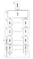
次いで、シリコンストリップ検出器11にて放射線を検出するため信号処理部の回路構成について説明する。図5は、実施の形態に係る信号処理部の回路構成を示すブロック図である。図5に示すように、信号処理部23は、増幅部41と、弁別部42と、演算部43と、出力部44とを備えている。
Next, the circuit configuration of the signal processing unit for detecting radiation with the
信号処理部23では、シリコンストリップ検出器11におけるストリップ電極16から出力されるパルス信号が増幅部41に入力されて増幅される。この増幅されたパルス信号は弁別部42において予め定められた閾値電圧と比較される。閾値電圧は、被検体3(図1参照)にて散乱した散乱X線による値と、被検体3を透過した透過X線による値との境界値となるよう被検体3に依存した最適な値が選択される。弁別部42では、閾値電圧未満のパルス信号が散乱X線のパルス信号、閾値電圧以上のパルス信号が透過X線のパルス信号として弁別され、散乱X線のパルス信号が除去される。
In the
弁別部42で弁別された透過X線のパルス信号は演算部43に入力される。演算部43では、透過X線のパルス信号を計数し、該パルス信号が波高分析されて複数のチャネルに弁別され、該チャネル毎にエネルギーの検出頻度が求められる。そして、波高分析後に各チャネルのエネルギーの検出頻度から放射線のエネルギー強度が求められる。
The transmitted X-ray pulse signal discriminated by the discriminating
上記の処理が全てのストリップ電極16それぞれの出力について行われ、演算部43では、各ストリップ電極16でのエネルギー強度のデータと、各ストリップ電極16の位置データとが関連付けられる。そして、関連付けられたデータは出力部44を介して外部機器46に出力される。外部機器46は、コンピュータ等を含み、演算部43で演算したデータに基づいてX線透過イメージを表示するためのデータが演算処理される。
The above processing is performed on the outputs of all the
以上のように、本実施の形態に係る放射線検出装置1では、シリコンストリップ検出器11の入射面11a側に、散乱X線を除去するコリメータを設けない構成としたが、上述した信号処理部23の処理によって散乱X線のパルス信号が除去することができる。これにより、本実施の形態では、コリメータを配置した分の不感領域をなくすことができ、X線検出の位置分解能を高めることができる。
As described above, in the radiation detection apparatus 1 according to the present embodiment, the collimator that removes scattered X-rays is not provided on the
また、上下に積層されるプリント基板14の間にスペーサ20を設けたので、ワイヤ18の形成空間を確保してワイヤ18による通電状態を良好に保つことができる。しかも、スペーサ20をできるだけ薄厚とすることでシリコンストリップ検出器11の上下間隔を小さくすることができ、上下方向における位置分解能を高密度化することができる。
In addition, since the
ここで、本実施の形態の比較構造として、シリコンストリップ検出器と実装体とが1枚のプリント基板で一体となる構成とすることが考えられる。この比較構造では、シリコンストリップ検出器と共に実装体も複数積層され、実装体に実装された回路等の厚みの制約を受けてシリコンストリップ検出器の上下間隔が大きくなる。この点、本実施の形態では、5枚のシリコンストリップ検出器11に対して実装体12を1枚としたので、実装体12における信号処理部23の厚みの制約を受けずにシリコンストリップ検出器11の上下間隔を小さくでき、これによっても、高い位置分解能を実現することができる。
Here, as a comparative structure of the present embodiment, it can be considered that the silicon strip detector and the mounting body are integrated with one printed board. In this comparative structure, a plurality of mounting bodies are stacked together with the silicon strip detector, and the vertical distance between the silicon strip detectors is increased under the restriction of the thickness of a circuit or the like mounted on the mounting body. In this regard, in this embodiment, since one mounting
本発明は上記実施の形態に限定されず種々変更して実施することが可能である。また、上記実施の形態で説明した数値、寸法、材質、方向については特に制限はない。その他、本発明の目的の範囲を逸脱しない限りにおいて適宜変更することが可能である。 The present invention is not limited to the above embodiment, and can be implemented with various modifications. Moreover, there is no restriction | limiting in particular about the numerical value, dimension, material, and direction which were demonstrated by the said embodiment. Other modifications may be made as appropriate without departing from the scope of the object of the present invention.
例えば、シリコンストリップ検出器11の枚数は複数であれば増減してもよい。また、実装体12の枚数も、シリコンストリップ検出器11より少ない枚数であれば、2枚以上設けてもよく、これによっても、シリコンストリップ検出器11の上下間隔を小さくすることができる。なお、一部の基板をシリコンストリップ検出器11と実装体12とで共通のものとしてもよい。
For example, the number of
また、弁別部42での閾値電圧は、上述した値に限定されるものでなく、変更してもよい。図6は、放射線検出時のエネルギースペクトルを示すグラフの一例であり、縦軸が計数(検出頻度)、横軸がエネルギー値を示している。光子と電子の相互作用の1つであるコンプトン散乱が起こる光子エネルギーの場合には、コンプトン散乱の連続的なスペクトルが観測される。このスペクトルは、γ線がエネルギーを与えそのまま180°折り返しす(散乱角180°の)場合が最も高く、ここをコンプトンエッジと呼ぶ。ここで、透過X線は入射面11aに真っ直ぐ入射してくるものの、散乱X線は不規則に入射してくる。したがって、図6に示すエネルギースペクトルとなる放射線においては、弁別部42での閾値として、同図のグラフのコンプトンエッジ近傍に設定するとよい。より具体的には、散乱角が150°の場合に対応したエネルギー値以上に設定され、より好ましくは、散乱角が170°の場合に対応したエネルギー値以上に設定されるとよい。これにより、散乱X線と透過X線との弁別を適切に実施可能となる。
Further, the threshold voltage in the
1 放射線検出装置
2 線形加速器
3 被検体
11 シリコンストリップ検出器(放射線検出体)
11a 入射面
12 実装体
14 プリント基板(検出体用基板)
15 半導体素子
16 ストリップ電極
20 スペーサ
22 主基板
23 信号処理部
42 弁別部
43 演算部
R X線(放射線)
DESCRIPTION OF SYMBOLS 1 Radiation detection apparatus 2
DESCRIPTION OF
Claims (7)
前記放射線検出体が検出した放射線のパルス信号を処理する信号処理部及び当該信号処理部が実装される主基板を有する実装体とを備え、前記放射線検出体の前記入射面側にコリメータを設けない放射線検出装置であって、
前記放射線検出体は、検出体用基板と、当該検出体用基板の面内に実装される半導体素子と、当該半導体素子の一方の主面に一軸方向に並列して配列され長手方向が前記入射面に直交する複数の短冊状のストリップ電極とを備え、
前記信号処理部は、前記放射線検出体の検出信号に応じ、被検体での散乱放射線のパルス信号と、透過放射線のパルス信号とを弁別する弁別部と、
前記弁別部で弁別された透過放射線のパルス信号を計数する演算部とを備え、
前記実装体の枚数は、前記放射線検出体の枚数より少ないことを特徴とする放射線検出装置。 A plurality of radiation detectors that are stacked in the thickness direction and detect radiation with one end surface as a radiation incident surface;
A signal processing unit that processes a pulse signal of radiation detected by the radiation detector, and a mounting body having a main substrate on which the signal processing unit is mounted, and no collimator is provided on the incident surface side of the radiation detector A radiation detection device comprising:
The radiation detection body is arranged in parallel in a uniaxial direction on one main surface of the semiconductor element, a semiconductor element mounted on the surface of the detection body substrate, and the semiconductor element mounted in the plane of the detection body. A plurality of strip-shaped strip electrodes orthogonal to the surface,
The signal processing unit is configured to discriminate a pulse signal of scattered radiation from a subject and a pulse signal of transmitted radiation according to a detection signal of the radiation detector,
A calculation unit that counts a pulse signal of the transmitted radiation discriminated by the discrimination unit;
The number of the mounting bodies is less than the number of the radiation detection bodies.
The threshold value used for discrimination in the discrimination unit is set to an energy value equal to or higher than the energy value corresponding to a scattering angle of 150 ° when the Compton edge scattering angle of transmitted radiation incident on the radiation detector is 180 °. The radiation detection apparatus according to claim 1, wherein the radiation detection apparatus is provided.
Priority Applications (1)
| Application Number | Priority Date | Filing Date | Title |
|---|---|---|---|
| JP2016029218A JP6591908B2 (en) | 2016-02-18 | 2016-02-18 | Radiation detector |
Applications Claiming Priority (1)
| Application Number | Priority Date | Filing Date | Title |
|---|---|---|---|
| JP2016029218A JP6591908B2 (en) | 2016-02-18 | 2016-02-18 | Radiation detector |
Publications (2)
| Publication Number | Publication Date |
|---|---|
| JP2017146244A JP2017146244A (en) | 2017-08-24 |
| JP6591908B2 true JP6591908B2 (en) | 2019-10-16 |
Family
ID=59683050
Family Applications (1)
| Application Number | Title | Priority Date | Filing Date |
|---|---|---|---|
| JP2016029218A Expired - Fee Related JP6591908B2 (en) | 2016-02-18 | 2016-02-18 | Radiation detector |
Country Status (1)
| Country | Link |
|---|---|
| JP (1) | JP6591908B2 (en) |
Families Citing this family (2)
| Publication number | Priority date | Publication date | Assignee | Title |
|---|---|---|---|---|
| JP7273842B2 (en) * | 2018-10-25 | 2023-05-15 | 株式会社東芝 | Photon-counting radiation detector and radiation inspection apparatus using the same |
| CN118234436A (en) * | 2021-11-24 | 2024-06-21 | 上海联影医疗科技股份有限公司 | Imaging Detector System |
Family Cites Families (7)
| Publication number | Priority date | Publication date | Assignee | Title |
|---|---|---|---|---|
| JPH07218642A (en) * | 1994-02-01 | 1995-08-18 | Hitachi Chem Co Ltd | Semiconductor radiation detector |
| JP2000321357A (en) * | 1999-03-10 | 2000-11-24 | Toshiba Corp | Nuclear medicine diagnostic equipment |
| JP4582022B2 (en) * | 2002-10-07 | 2010-11-17 | 株式会社日立製作所 | Radiation detector, radiation detection element, and radiation imaging apparatus |
| JP4413874B2 (en) * | 2006-02-06 | 2010-02-10 | 住友重機械工業株式会社 | Radiation detection unit and radiation inspection apparatus |
| JP4621188B2 (en) * | 2006-09-29 | 2011-01-26 | 株式会社日立製作所 | Nuclear medicine diagnostic equipment |
| JP2008227117A (en) * | 2007-03-13 | 2008-09-25 | Hitachi Ltd | Semiconductor radiation detector and industrial X-ray CT apparatus using the same |
| JP5027832B2 (en) * | 2009-02-17 | 2012-09-19 | 株式会社日立製作所 | Radiation detection module and radiation imaging apparatus |
-
2016
- 2016-02-18 JP JP2016029218A patent/JP6591908B2/en not_active Expired - Fee Related
Also Published As
| Publication number | Publication date |
|---|---|
| JP2017146244A (en) | 2017-08-24 |
Similar Documents
| Publication | Publication Date | Title |
|---|---|---|
| JP6456854B2 (en) | Radiation imaging device | |
| US8110809B2 (en) | Radiation detector and radiographic inspection apparatus | |
| WO2008018534A1 (en) | Gamma ray detector | |
| US12183844B2 (en) | Radiation detection element, radiation detector and radiation detection device | |
| CN205015485U (en) | Detector subassembly and X -ray detector | |
| US7265359B2 (en) | Method and device for detecting fast neutrons | |
| US9054260B2 (en) | Radiation detecting element and radiation detecting device | |
| CN106324649A (en) | Semiconductor detector | |
| CN113874758B (en) | Panel Radiation Detector | |
| JP6591908B2 (en) | Radiation detector | |
| JP2016035437A (en) | Compton camera detector and Compton camera | |
| US20140119512A1 (en) | X-ray detector and x-ray diffraction device | |
| JP4464998B2 (en) | Semiconductor detector module, and radiation detection apparatus or nuclear medicine diagnostic apparatus using the semiconductor detector module | |
| CN108345024A (en) | Detection device and detection method | |
| Matteson et al. | Charge collection studies of a high resolution CZT-based detector for PET | |
| JP2009156740A (en) | Radiation detection apparatus | |
| JP6780429B2 (en) | Radiation detector | |
| CN118339621A (en) | Target collimation for detectors using post-collimators | |
| JP2004354271A (en) | Radiation detector | |
| JP4748567B2 (en) | Radiation incident position detector | |
| JP5403423B2 (en) | High energy X-ray energy discrimination inspection device and inspection method | |
| Vanier et al. | Demonstration of a directional fast neutron detector | |
| JPH0732968U (en) | Radiation detector | |
| JP7496181B1 (en) | Measuring device and measuring method | |
| US7639783B1 (en) | Parallax free and spark protected X-ray detector |
Legal Events
| Date | Code | Title | Description |
|---|---|---|---|
| RD01 | Notification of change of attorney |
Free format text: JAPANESE INTERMEDIATE CODE: A7426 Effective date: 20160318 |
|
| A521 | Request for written amendment filed |
Free format text: JAPANESE INTERMEDIATE CODE: A821 Effective date: 20160318 |
|
| A80 | Written request to apply exceptions to lack of novelty of invention |
Free format text: JAPANESE INTERMEDIATE CODE: A80 Effective date: 20160318 |
|
| A621 | Written request for application examination |
Free format text: JAPANESE INTERMEDIATE CODE: A621 Effective date: 20181025 |
|
| A521 | Request for written amendment filed |
Free format text: JAPANESE INTERMEDIATE CODE: A821 Effective date: 20181025 |
|
| A977 | Report on retrieval |
Free format text: JAPANESE INTERMEDIATE CODE: A971007 Effective date: 20190813 |
|
| TRDD | Decision of grant or rejection written | ||
| A01 | Written decision to grant a patent or to grant a registration (utility model) |
Free format text: JAPANESE INTERMEDIATE CODE: A01 Effective date: 20190820 |
|
| A61 | First payment of annual fees (during grant procedure) |
Free format text: JAPANESE INTERMEDIATE CODE: A61 Effective date: 20190919 |
|
| R150 | Certificate of patent or registration of utility model |
Ref document number: 6591908 Country of ref document: JP Free format text: JAPANESE INTERMEDIATE CODE: R150 |
|
| LAPS | Cancellation because of no payment of annual fees |