JP6588731B2 - Electrophotographic photosensitive member, process cartridge, and electrophotographic apparatus - Google Patents
Electrophotographic photosensitive member, process cartridge, and electrophotographic apparatus Download PDFInfo
- Publication number
- JP6588731B2 JP6588731B2 JP2015094849A JP2015094849A JP6588731B2 JP 6588731 B2 JP6588731 B2 JP 6588731B2 JP 2015094849 A JP2015094849 A JP 2015094849A JP 2015094849 A JP2015094849 A JP 2015094849A JP 6588731 B2 JP6588731 B2 JP 6588731B2
- Authority
- JP
- Japan
- Prior art keywords
- photosensitive member
- electrophotographic photosensitive
- layer
- boron nitride
- electrophotographic
- Prior art date
- Legal status (The legal status is an assumption and is not a legal conclusion. Google has not performed a legal analysis and makes no representation as to the accuracy of the status listed.)
- Active
Links
Images

Classifications
-
- G—PHYSICS
- G03—PHOTOGRAPHY; CINEMATOGRAPHY; ANALOGOUS TECHNIQUES USING WAVES OTHER THAN OPTICAL WAVES; ELECTROGRAPHY; HOLOGRAPHY
- G03G—ELECTROGRAPHY; ELECTROPHOTOGRAPHY; MAGNETOGRAPHY
- G03G5/00—Recording members for original recording by exposure, e.g. to light, to heat, to electrons; Manufacture thereof; Selection of materials therefor
- G03G5/02—Charge-receiving layers
- G03G5/04—Photoconductive layers; Charge-generation layers or charge-transporting layers; Additives therefor; Binders therefor
- G03G5/05—Organic bonding materials; Methods for coating a substrate with a photoconductive layer; Inert supplements for use in photoconductive layers
- G03G5/0503—Inert supplements
- G03G5/0507—Inorganic compounds
-
- G—PHYSICS
- G03—PHOTOGRAPHY; CINEMATOGRAPHY; ANALOGOUS TECHNIQUES USING WAVES OTHER THAN OPTICAL WAVES; ELECTROGRAPHY; HOLOGRAPHY
- G03G—ELECTROGRAPHY; ELECTROPHOTOGRAPHY; MAGNETOGRAPHY
- G03G5/00—Recording members for original recording by exposure, e.g. to light, to heat, to electrons; Manufacture thereof; Selection of materials therefor
- G03G5/14—Inert intermediate or cover layers for charge-receiving layers
- G03G5/147—Cover layers
- G03G5/14704—Cover layers comprising inorganic material
Description
本発明は、電子写真感光体ならびに、電子写真感光体を有するプロセスカートリッジおよび電子写真感光体を有する電子写真装置に関する。 The present invention relates to an electrophotographic photosensitive member, a process cartridge having an electrophotographic photosensitive member, and an electrophotographic apparatus having an electrophotographic photosensitive member.
電子写真感光体や中間転写体の表面の転写残トナーを除去する方法として、例えば、ブラシ形状やブレード形状のクリーニング部材を電子写真感光体や中間転写体の表面に当接させて不要物を掻き取る方法や、不要物を吸引除去する方法が知られている。これらの中でも、ブレード形状のクリーニング部材、いわゆるクリーニングブレードを用いる方法は、簡単な構成で効率的にクリーニングを行うことができるため、広く用いられている方法である。 As a method of removing the transfer residual toner on the surface of the electrophotographic photosensitive member or intermediate transfer member, for example, a brush-shaped or blade-shaped cleaning member is brought into contact with the surface of the electrophotographic photosensitive member or intermediate transfer member to scrape unnecessary materials. There are known methods for removing and removing unnecessary substances by suction. Among these, a method using a blade-shaped cleaning member, a so-called cleaning blade, is a widely used method because it can be efficiently cleaned with a simple configuration.
クリーニングブレードの材質としては、電子写真感光体や中間転写体の表面との密着性を確保しやすいゴム(特にウレタンゴム)が用いられることが多い。一方で、ゴムは、摩擦係数が高い材料でもある。そのため、異音の発生(ブレード鳴き)や、クリーニングブレードの振動によるトナーの掻き取り能力の低下(トナー摺り抜け)や、クリーニングブレードが捲れる現象(ブレード捲れ)が発生し、電子写真感光体の駆動トルクを確保するために多くのエネルギーを要する原因となっていた。 As the material of the cleaning blade, rubber (especially urethane rubber) that can easily secure adhesion to the surface of the electrophotographic photosensitive member or the intermediate transfer member is often used. On the other hand, rubber is also a material with a high coefficient of friction. Therefore, abnormal noise (blade squealing), reduction of toner scraping ability due to vibration of the cleaning blade (toner slipping), and a phenomenon that the cleaning blade is swollen (blade curl) occur. It has become a cause that requires a lot of energy to secure the driving torque.
これらの課題を解決する手法として、例えば特許文献1にはフッ素樹脂成分を電子写真感光体の表面層に含有させる方法が開示されており、また特許文献2には、金属石鹸と無機微粒子を感光体周辺から供給する機構が開示されている。 As a technique for solving these problems, for example, Patent Document 1 discloses a method in which a fluororesin component is included in the surface layer of an electrophotographic photosensitive member, and Patent Document 2 discloses a method in which metal soap and inorganic fine particles are exposed. A mechanism for supplying from around the body is disclosed.
しかしながら、特許文献1に記載の方法では、特にフッ素樹脂成分の含有量が少ない時は、初期の感光体の摩擦係数を低減することはできても、耐久中の放電履歴等により材料が劣化し、摩擦係数の上昇を招きやすい。一方で、フッ素樹脂成分の含有量が多くなると、フッ素樹脂成分の結着樹脂への分散性が悪化し、またフッ素樹脂は屈折率が小さいため、レーザー光を散乱し、静電潜像や電位コントラストの不良を引き起こし、異常画像が発生する場合がある。 However, in the method described in Patent Document 1, particularly when the content of the fluororesin component is small, the friction coefficient of the initial photoreceptor can be reduced, but the material deteriorates due to the discharge history during the durability. It tends to increase the friction coefficient. On the other hand, when the content of the fluororesin component increases, the dispersibility of the fluororesin component into the binder resin deteriorates, and since the fluororesin has a low refractive index, it scatters laser light, causing electrostatic latent images and potentials An abnormal image may occur due to a poor contrast.
また、特許文献2に記載の方法についても、感光体周辺から供給ユニットを通じて材料が供給されるため、装置の大型化、複雑化が避けられず、生産性の低下、コストアップを発生させる。また、摩擦特性についても、金属石鹸については速やかに放電劣化が起き、摩擦係数が上昇するため、供給量が多くなりフィルミング等により画像不良を発生しやすい。また併用されている窒化ホウ素は、一定の耐放電性が認められるものの、金属石鹸もしくは感光体表面層に付着しているだけであり、十分に劈開性を発現することができず、感光体表面の摩擦係数低下に十分に寄与することができないものであった。 In the method described in Patent Document 2, since the material is supplied from the periphery of the photoreceptor through the supply unit, the apparatus is inevitably increased in size and complexity, resulting in a decrease in productivity and an increase in cost. In addition, with regard to the friction characteristics, since the metal soap quickly undergoes discharge deterioration and the friction coefficient increases, the supply amount increases, and image defects are likely to occur due to filming or the like. In addition, boron nitride used in combination has a certain discharge resistance, but it is only attached to the metal soap or the surface layer of the photoconductor, and cannot sufficiently exhibit the cleaving property. It was not possible to sufficiently contribute to lowering the friction coefficient.
本発明の目的は、耐久使用中に渡って、表面の潤滑性(低摩擦性)に優れた電子写真感光体、ならびに、該電子写真感光体を有するプロセスカートリッジおよび電子写真装置を提供することにある。 An object of the present invention is to provide an electrophotographic photoreceptor excellent in surface lubricity (low friction) during durability use, and a process cartridge and an electrophotographic apparatus having the electrophotographic photoreceptor. is there.
支持体と、前記支持体上に設けられた感光層と、を有する電子写真感光体であって、前記電子写真感光体の最表面層が結着樹脂を含有し、前記最表面層の結着樹脂に六方晶窒化ホウ素が分散されており、かつ、前記六方晶窒化ホウ素の黒鉛化指数(GI)が3.0以上15.0未満であり、および前記六方晶窒化ホウ素の最表面層の体積に対する含有割合が1体積%〜20体積%であることを特徴とする電子写真感光体である。 An electrophotographic photosensitive member having a support and a photosensitive layer provided on the support, wherein the outermost surface layer of the electrophotographic photosensitive member contains a binder resin, and the binding of the outermost surface layer hexagonal boron nitride in the resin are dispersed, and, of the hexagonal boron nitride graphitization index (GI) is Ri der less 15.0 3.0 or more, and the outermost surface layer of said hexagonal boron nitride proportion to volume is an electrophotographic photosensitive member according to claim 20 vol% der Rukoto 1 vol%.
また、本発明は、上記電子写真感光体と、前記電子写真感光体の表面を帯電させる帯電手段、トナーを用いて前記電子写真感光体上に形成された静電潜像を現像してトナー画像を形成する現像手段、前記電子写真感光体上に形成された前記トナー画像を転写材に転写する転写手段、および前記電子写真感光体の表面に当接しながら当該電子写真感光体をクリーニングするクリーニングブレードを有するクリーニング手段からなる群より選択される少なくとも1つの手段とを一体に支持し、電子写真装置本体に着脱自在であることを特徴とするプロセスカートリッジである。 The present invention also provides a toner image obtained by developing the electrophotographic photosensitive member, a charging unit for charging the surface of the electrophotographic photosensitive member, and a toner to develop an electrostatic latent image formed on the electrophotographic photosensitive member. Developing means for forming the toner image, transfer means for transferring the toner image formed on the electrophotographic photosensitive member to a transfer material, and a cleaning blade for cleaning the electrophotographic photosensitive member while contacting the surface of the electrophotographic photosensitive member A process cartridge characterized in that it integrally supports at least one means selected from the group consisting of cleaning means, and is detachable from the electrophotographic apparatus main body.
また、本発明は、上記電子写真感光体と、前記電子写真感光体の表面を帯電させる帯電手段と、帯電された前記電子写真感光体を露光して像様に静電潜像を形成する画像露光手段と、トナーを用いて前記電子写真感光体上に形成された前記静電潜像を現像してトナー画像を形成する現像手段と、前記電子写真感光体上に形成された前記トナー画像を転写材に転写する転写手段と、該電子写真感光体の表面に当接しながら当該電子写真感光体をクリーニングするクリーニングブレードを有するクリーニング手段とを有する電子写真装置である。 The present invention also provides an image for forming an electrostatic latent image in an image-like manner by exposing the electrophotographic photosensitive member, a charging unit for charging the surface of the electrophotographic photosensitive member, and the charged electrophotographic photosensitive member. An exposure means, a developing means for developing the electrostatic latent image formed on the electrophotographic photosensitive member using toner to form a toner image, and the toner image formed on the electrophotographic photosensitive member An electrophotographic apparatus comprising: a transfer unit that transfers to a transfer material; and a cleaning unit that includes a cleaning blade that cleans the electrophotographic photosensitive member while being in contact with the surface of the electrophotographic photosensitive member.
本発明によれば、電子写真感光体における表面の潤滑性に優れ、その潤滑性が放電を受けても維持されるため、耐久性に優れた電子写真感光体ならびに、該電子写真感光体を有するプロセスカートリッジおよび電子写真装置を提供することができる。 According to the present invention, the electrophotographic photosensitive member has excellent surface lubricity, and the lubricity is maintained even after being discharged. Therefore, the electrophotographic photosensitive member having excellent durability and the electrophotographic photosensitive member are provided. A process cartridge and an electrophotographic apparatus can be provided.
(電子写真感光体)
本発明における第一の実施形態は、最表面層の結着樹脂に六方晶窒化ホウ素が分散されており、かつ、前記六方晶窒化ホウ素の黒鉛化指数(GI)が3.0以上15.0未満であることを特徴とする電子写真感光体である。
(Electrophotographic photoreceptor)
In the first embodiment of the present invention, hexagonal boron nitride is dispersed in the binder resin of the outermost surface layer, and the graphitization index (GI) of the hexagonal boron nitride is 3.0 or more and 15.0. The electrophotographic photosensitive member is characterized by being less than the above.
ここで、本発明における窒化ホウ素は、六方晶の結晶型を有する窒化ホウ素であり、燐片状に結晶が成長しているものをいう。六方晶窒化ホウ素は、黒鉛同様、窒化ホウ素の平面構造がファンデルワールス力により積層構造を形成しているものであり、せん断力により積層構造が劈開するという性質を有しているため、低摩擦係数を有する材料である。また、有機物に比べて結合エネルギーや耐熱性が高く、電子写真プロセスにおける放電に対して材料耐性が高い材料でもある。 Here, the boron nitride in the present invention is a boron nitride having a hexagonal crystal type, and means that crystals grow in the form of flakes. Hexagonal boron nitride, like graphite, has the property that the planar structure of boron nitride forms a laminated structure by van der Waals force, and the laminated structure is cleaved by shearing force. A material having a coefficient. In addition, it is a material having higher binding energy and heat resistance than organic materials and high material resistance against discharge in an electrophotographic process.
本発明における六方晶窒化ホウ素の結晶化度は、黒鉛化指数(GI)で定義する。ここでGI(Graphitization Index)はX線回折図の(100)、(101)及び(102)線の積分強度比すなわち面積比を、GI=〔面積{(100)+(101)}〕/〔面積(102)〕、の計算によって求めるものである(J.Thomas,et.al,J.Am.Chem.Soc.84,4619(1962))。GIは鱗片状である六方晶窒化ホウ素の結晶性の指標であり、この値が小さいほど結晶性が高いことが知られている。本発明は、上記六方晶窒化ホウ素のGIが3.0以上15.0未満であることを特徴とする。すなわち、結晶化度が比較的低い六方晶窒化ホウ素を用いることを特徴とする。 The crystallinity of hexagonal boron nitride in the present invention is defined by the graphitization index (GI). Here, GI (Graphization Index) is the integrated intensity ratio of the (100), (101) and (102) lines of the X-ray diffraction diagram, that is, the area ratio, GI = [area {(100) + (101)}] / [ Area (102)] (J. Thomas, et.al, J. Am. Chem. Soc. 84, 4619 (1962)). GI is an index of crystallinity of hexagonal boron nitride that is in the form of scales, and it is known that the smaller this value, the higher the crystallinity. The present invention is characterized in that the GI of the hexagonal boron nitride is 3.0 or more and less than 15.0. That is, hexagonal boron nitride having a relatively low crystallinity is used.
一般に、同様の六方晶の結晶構造を有する黒鉛では結晶化度が高いほど劈開しやすく、低摩擦係数を発現することが知られている。しかし、本発明者らが鋭意検討した結果、窒化ホウ素を電子写真感光体の最表面層に含有させて検討したところ、結晶化度が高いほど劈開し易いわけではなく、上記GIの範囲外(3.0未満)においては、むしろ逆の傾向があることを見出した。 In general, it is known that graphite having a similar hexagonal crystal structure is more easily cleaved as the degree of crystallinity is higher, and exhibits a low coefficient of friction. However, as a result of intensive studies by the present inventors, boron nitride was included in the outermost surface layer of the electrophotographic photosensitive member, and as a result, the higher the crystallinity, the easier it was to cleave, and it was out of the above GI range ( In less than 3.0), the reverse tendency was found.
六方晶窒化ホウ素のゼータ電位測定、及び結着樹脂分散膜の断面SEM観察の結果、GIが3.0未満では発達した結晶のため六方晶窒化ホウ素粒子同士の凝集が起きにくく、結着樹脂に包埋されやすいことがわかった。そのため、クリーニングブレード等から最面表層にせん断力がかかった際、劈開現象が起こりにくくなり、摩擦係数が大きくなる。また、GIが15.0以上となると、そもそも結晶化度が小さいため、六方晶窒化ホウ素の劈開が起こりにくく、摩擦係数が大きくなる。 As a result of the zeta potential measurement of hexagonal boron nitride and the cross-sectional SEM observation of the binder resin dispersion film, the GI is less than 3.0, so that the agglomerated hexagonal boron nitride particles hardly occur due to the developed crystals. It turns out that it is easy to be embedded. Therefore, when a shearing force is applied to the outermost surface layer from a cleaning blade or the like, the cleavage phenomenon is less likely to occur and the friction coefficient is increased. On the other hand, when the GI is 15.0 or more, the degree of crystallinity is small in the first place, so that the hexagonal boron nitride is hardly cleaved, and the friction coefficient increases.
一方、本発明のようにGIが3.0以上15.0未満である六方晶窒化ホウ素を用いると、比較的小さな結晶化度のため、六方晶窒化ホウ素粒子同士の親和性が大きく、結着樹脂へ分散した際も、結着樹脂による包埋が起きにくい。そのため、分散膜中でも六方晶窒化ホウ素粒子の劈開が阻害されにくく、低摩擦係数を実現することができる。本発明に好適に用いられるGIの範囲として4.0以上11.0以下であるとさらに好ましい。 On the other hand, when hexagonal boron nitride having a GI of 3.0 or more and less than 15.0 is used as in the present invention, the affinity between hexagonal boron nitride particles is large due to relatively small crystallinity, and binding Even when dispersed in a resin, embedding with a binder resin is unlikely to occur. Therefore, cleavage of hexagonal boron nitride particles is hardly inhibited even in the dispersion film, and a low friction coefficient can be realized. The range of GI preferably used in the present invention is more preferably 4.0 or more and 11.0 or less.
さらに検討した結果、本発明のように六方晶窒化ホウ素を結着樹脂に分散した膜は、六方晶窒化ホウ素を外部添加により表面に塗布した膜より、摩擦係数が低下することがわかった。これは、本発明に係る範囲内のGIを有する六方晶窒化ホウ素を用いた場合、上述したように部分的に六方晶窒化ホウ素が樹脂と接し固定されている影響で、最表層表面に塗布している状態より、せん断のエネルギー散逸が減少し、効率的に劈開が起こるためであると考えられる。 As a result of further investigation, it was found that a film in which hexagonal boron nitride is dispersed in a binder resin as in the present invention has a lower friction coefficient than a film in which hexagonal boron nitride is applied to the surface by external addition. This is because when hexagonal boron nitride having a GI within the range according to the present invention is used, the hexagonal boron nitride is applied to the surface of the outermost layer due to the influence of the hexagonal boron nitride being in contact with the resin and being fixed as described above. It is thought that the energy dissipation of the shear is reduced and the cleavage is efficiently performed.
本発明において、最表面層における六方晶窒化ホウ素の含有割合は1体積%〜20体積%であることが好ましい。さらに好ましくは5体積%〜15体積%である。この六方晶窒化ホウ素の含有割合は、従来電子写真感光体表層に潤滑性を付与するために用いられてきた種々のフィラー、例えばポリテトラフルオロエチレン(PTFE)の含有割合に比較して、少ない量である。六方晶窒化ホウ素の含有量が1体積%未満では、十分な潤滑性が得られない場合がある。また六方晶窒化ホウ素の含有割合が20体積%より多いと、六方晶窒化ホウ素の分散性が悪化し、レーザー光の透過性が損なわれ、画像不良の原因となる場合がある。 In the present invention, the content ratio of hexagonal boron nitride in the outermost surface layer is preferably 1% by volume to 20% by volume. More preferably, it is 5 volume%-15 volume%. The content ratio of this hexagonal boron nitride is small compared to the content ratios of various fillers conventionally used for imparting lubricity to the surface layer of the electrophotographic photoreceptor, such as polytetrafluoroethylene (PTFE). It is. If the content of hexagonal boron nitride is less than 1% by volume, sufficient lubricity may not be obtained. On the other hand, when the content of hexagonal boron nitride is more than 20% by volume, the dispersibility of hexagonal boron nitride is deteriorated, the laser beam transmittance is impaired, and image defects may be caused.
本発明において、六方晶窒化ホウ素の平均粒子径は0.1〜10μmであることが好ましい。 In the present invention, the average particle size of hexagonal boron nitride is preferably 0.1 to 10 μm.
また、本発明における六方晶窒化ホウ素は、表面(結晶の端部)に存在するアミノ基や水酸基等の極性官能基が疎水的に処理されていてもよい。六方晶窒化ホウ素が有する極性官能基が疎水的に処理されていることにより、電子写真感光体の電位特性、潤滑効果をさらに高めることができる。六方晶窒化ホウ素はホウ酸、酸化ホウ素、ホウ砂などのホウ素化合物とメラミン、尿素、ジシアンアミドなどの窒素含有化合物とを混合し、焼成する等の方法により製造することができる。六方晶窒化ホウ素の結晶化度は焼成条件により制御することができ、特に焼成温度に大きく依存する。例えば1600℃以上においては、焼成温度の増加に伴いGI値が減少し、結晶化度が向上することが知られている。 Further, in the hexagonal boron nitride in the present invention, polar functional groups such as amino groups and hydroxyl groups present on the surface (crystal ends) may be treated hydrophobicly. Since the polar functional group of hexagonal boron nitride is treated hydrophobicly, the potential characteristics and lubrication effect of the electrophotographic photoreceptor can be further enhanced. Hexagonal boron nitride can be produced by a method in which a boron compound such as boric acid, boron oxide, or borax and a nitrogen-containing compound such as melamine, urea, or dicyanamide are mixed and fired. The degree of crystallinity of hexagonal boron nitride can be controlled by firing conditions, and particularly depends greatly on the firing temperature. For example, at 1600 ° C. or higher, it is known that the GI value decreases as the firing temperature increases and the crystallinity improves.
ここで疎水的処理とは、シランカップリング反応、エステル反応、イソシアネート反応等の方法により、種々の疎水基を有する分子ユニットを六方晶窒化ホウ素表面に共有結合を介して導入することを言う。本発明における疎水的処理は操作の簡便性の観点から、シランカップリング剤によるシランカップリング反応を用いることが好ましい。ここで疎水基とは、C1〜C18の直鎖状もしくは枝分れ状のアルキル基、前記アルキル基中の一部の炭素原子が二重結合炭素、三重結合炭素、芳香族炭素で置換されているもの、前記アルキル基中の一部もしくは全部の水素原子がフッ素原子、シクロアルキル基、アリール基で置換されたもの、またこれらを含有するものをいう。これらのうち、フッ素原子を含有するもの、C8以上のアルキル鎖長を含有するものは、潤滑効果の観点から特に好適に用いることができる。また、反応生成物の感光体特性への影響を考慮し、塩素原子を含まないシランカップリング剤を用いることが好ましい。
以下に、本発明に用いられるシランカップリング剤の構造を例示するが、本発明はこれらに限定されるものではない。
Here, the hydrophobic treatment means that molecular units having various hydrophobic groups are introduced into the hexagonal boron nitride surface via a covalent bond by a method such as a silane coupling reaction, an ester reaction, or an isocyanate reaction. The hydrophobic treatment in the present invention preferably uses a silane coupling reaction with a silane coupling agent from the viewpoint of simplicity of operation. Here, the hydrophobic group is a C1-C18 linear or branched alkyl group, in which some carbon atoms in the alkyl group are substituted with double bond carbon, triple bond carbon, or aromatic carbon. And those in which some or all of the hydrogen atoms in the alkyl group are substituted with fluorine atoms, cycloalkyl groups, and aryl groups, and those containing these. Among these, those containing a fluorine atom and those containing an alkyl chain length of C8 or more can be particularly preferably used from the viewpoint of the lubricating effect. In consideration of the influence of the reaction product on the characteristics of the photoreceptor, it is preferable to use a silane coupling agent that does not contain a chlorine atom.
Although the structure of the silane coupling agent used for this invention is illustrated below, this invention is not limited to these.

次に、電子写真感光体の層構成について説明する。 Next, the layer structure of the electrophotographic photoreceptor will be described.
電子写真感光体は、一般的に、支持体および該支持体上に形成された感光層を有する。
感光層は、電荷輸送物質と電荷発生物質とを同一の層に含有させてなる単層型の感光層であってもよいし、電荷発生物質を含有する電荷発生層と電荷輸送物質を含有する電荷輸送層とを積層してなる積層型の感光層であってもよい。また、積層型の感光層は、支持体側から電荷発生層、電荷輸送層の順に積層してなる順層型の感光層が好ましい。
An electrophotographic photoreceptor generally has a support and a photosensitive layer formed on the support.
The photosensitive layer may be a single-layer type photosensitive layer containing a charge transport material and a charge generation material in the same layer, or contains a charge generation layer containing a charge generation material and a charge transport material. It may be a laminate type photosensitive layer formed by laminating a charge transport layer. In addition, the multilayer photosensitive layer is preferably a normal photosensitive layer formed by laminating a charge generation layer and a charge transport layer in this order from the support side.
また、感光層上に保護層を設けて最表面層としてもよい。保護層は、導電性金属酸化物粒子などの導電性粒子を含有してもよい。保護層用の結着樹脂としては、表面硬度が硬く、耐磨耗性に優れる点から硬化性樹脂がより好ましい。硬化性樹脂としては、アクリル樹脂、ウレタン樹脂、エポキシ樹脂、シリコーン樹脂、フェノール樹脂等が挙げられるが、これらに限定されるものではない。保護層の膜厚は、0.5〜10μmであることが好ましく、特には、1〜7μmであることが好ましい。 Further, a protective layer may be provided on the photosensitive layer to form the outermost surface layer. The protective layer may contain conductive particles such as conductive metal oxide particles. As the binder resin for the protective layer, a curable resin is more preferable because of its high surface hardness and excellent wear resistance. Examples of the curable resin include, but are not limited to, an acrylic resin, a urethane resin, an epoxy resin, a silicone resin, and a phenol resin. The thickness of the protective layer is preferably 0.5 to 10 μm, and particularly preferably 1 to 7 μm.
ここで電子写真感光体の最表面層とは、電子写真感光体の最表面に位置する層(支持体から最も離隔した層)を意味する。例えば、保護層を設ける場合、電子写真感光体の最表面層は保護層である。保護層を設けない場合であって感光層が単層型の感光層である場合、電子写真感光体の最表面層は単層型の感光層である。保護層を設けない場合であって感光層が順層型の感光層である場合、電子写真感光体の最表面層は電荷輸送層である。 Here, the outermost surface layer of the electrophotographic photosensitive member means a layer (a layer farthest from the support) located on the outermost surface of the electrophotographic photosensitive member. For example, when a protective layer is provided, the outermost surface layer of the electrophotographic photosensitive member is a protective layer. When the protective layer is not provided and the photosensitive layer is a single layer type photosensitive layer, the outermost surface layer of the electrophotographic photosensitive member is a single layer type photosensitive layer. When the protective layer is not provided and the photosensitive layer is a normal layer type photosensitive layer, the outermost surface layer of the electrophotographic photosensitive member is a charge transport layer.
支持体としては、導電性を有するもの(導電性支持体)が好ましい。具体的には、アルミニウム、ニッケル、銅、金、鉄などの金属またはこれらの複数からなる合金製の支持体や、ポリエステル、ポリカーボネート、ポリイミド、ガラスなどの絶縁性支持体上にアルミニウム、銀、金などの金属または酸化インジウム、酸化スズなどの導電性材料の薄膜を形成してなるものや、カーボンブラックまたは導電性フィラーを樹脂中に分散し、導電性を付与してなるものなどが挙げられる。 As a support body, what has electroconductivity (conductive support body) is preferable. Specifically, a support made of a metal such as aluminum, nickel, copper, gold, iron or an alloy made of a plurality of these, or an insulating support such as polyester, polycarbonate, polyimide, glass, aluminum, silver, gold, etc. Examples include those obtained by forming a thin film of a conductive material such as metal or indium oxide or tin oxide, and those obtained by dispersing carbon black or a conductive filler in a resin to impart conductivity.
支持体の表面には、電気的特性や密着性の改善のために、陽極酸化などの電気化学的な処理を施すことができる。また、支持体の表面を、アルカリリン酸塩やリン酸やタンニン酸を主成分とする酸性水溶液に金属塩の化合物やフッ素化合物の金属塩を溶解してなる溶液で化学処理を施すこともできる。 The surface of the support can be subjected to an electrochemical treatment such as anodization in order to improve electrical characteristics and adhesion. Further, the surface of the support can be subjected to chemical treatment with a solution obtained by dissolving a metal salt compound or a fluorine compound metal salt in an acidic aqueous solution mainly composed of alkali phosphate, phosphoric acid or tannic acid. .
また、レーザー光などの単一波長光を画像露光光として用いる場合、干渉縞を抑制するため、支持体の表面を粗面化することが好ましい。具体的には、支持体の表面を、ホーニング、ブラスト、切削、電界研磨などの処理を施したり、支持体の表面に導電性金属酸化物および結着樹脂からなる導電性皮膜を設けたりすることによって、支持体の表面を粗面化することができる。 Moreover, when using single wavelength light, such as a laser beam, as image exposure light, in order to suppress an interference fringe, it is preferable to roughen the surface of a support body. Specifically, the surface of the support is subjected to processing such as honing, blasting, cutting, and electropolishing, or a conductive film made of a conductive metal oxide and a binder resin is provided on the surface of the support. Thus, the surface of the support can be roughened.
ホーニング処理としては、乾式および湿式での処理方法がある。湿式ホーニング処理は、水などの液体に粉末状の研磨剤を懸濁させ、高速度で支持体の表面に吹き付けて、支持体の表面を粗面化する方法である。支持体の表面粗さは、吹き付け圧力、速度、研磨剤の量、種類、形状、大きさ、硬度、比重、懸濁温度などにより制御することができる。乾式ホーニング処理は、研磨剤をエアーにより、高速度で支持体の表面に吹き付けて、支持体の表面を粗面化する方法であり、湿式ホーニング処理と同じようにして、支持体の表面粗さを制御することができる。ホーニング処理に用いられる研磨剤としては、例えば、炭化ケイ素、アルミナ、鉄、ガラスなどの粒子が挙げられる。 As the honing treatment, there are dry and wet treatment methods. The wet honing treatment is a method in which a powdery abrasive is suspended in a liquid such as water and sprayed onto the surface of the support at a high speed to roughen the surface of the support. The surface roughness of the support can be controlled by spraying pressure, speed, amount of abrasive, type, shape, size, hardness, specific gravity, suspension temperature, and the like. The dry honing process is a method in which the surface of the support is roughened by spraying an abrasive on the surface of the support with air at a high speed. The surface roughness of the support is the same as in the wet honing process. Can be controlled. As an abrasive | polishing agent used for a honing process, particles, such as silicon carbide, an alumina, iron, glass, are mentioned, for example.
支持体と感光層または後述の下引き層との間には、レーザー光などの単一波長光による干渉縞の抑制や、支持体の表面の傷の被覆を目的とした導電層を設けてもよい。
導電層は、カーボンブラック、金属粒子、金属酸化物粒子などの導電性粒子を結着樹脂および溶剤とともに分散処理することによって得られる導電層用塗布液を塗布し、得られた塗膜を乾燥/硬化させることによって形成することができる。金属酸化物粒子としては、例えば、酸化亜鉛粒子、酸化チタン粒子などが挙げられる。また、導電性粒子として、硫酸バリウム粒子を用いることもできる。また、導電性粒子は、芯材粒子に被覆層を設けてなる複合粒子であってもよい。
A conductive layer may be provided between the support and the photosensitive layer or the undercoat layer described below for the purpose of suppressing interference fringes by single-wavelength light such as laser light and covering scratches on the surface of the support. Good.
The conductive layer is obtained by applying a conductive layer coating solution obtained by dispersing conductive particles such as carbon black, metal particles, and metal oxide particles together with a binder resin and a solvent, and drying the obtained coating film. It can be formed by curing. Examples of the metal oxide particles include zinc oxide particles and titanium oxide particles. Also, barium sulfate particles can be used as the conductive particles. The conductive particles may be composite particles obtained by providing a coating layer on the core material particles.
導電性粒子の体積抵抗率は、0.1〜1000Ω・cmであることが好ましく、1〜1000Ω・cmであることがより好ましい。この体積抵抗率は、三菱油化(株)(現:(株)三菱化学アナリテック)製の抵抗測定装置ロレスタAPを用いて測定して求めた値である。測定サンプルは、導電性粒子を49MPaの圧力で固めてコイン状としたものである。 The volume resistivity of the conductive particles is preferably 0.1 to 1000 Ω · cm, and more preferably 1 to 1000 Ω · cm. The volume resistivity is a value obtained by measurement using a resistance measuring apparatus Loresta AP manufactured by Mitsubishi Oil Chemical Co., Ltd. (currently Mitsubishi Chemical Analytech Co., Ltd.). The measurement sample is obtained by solidifying conductive particles with a pressure of 49 MPa to form a coin.
導電性粒子の平均粒径は、0.05〜1.0μmであることが好ましく、0.07〜0.7μmであることがより好ましい。この平均粒径は、遠心沈降法により測定した値である。 The average particle size of the conductive particles is preferably 0.05 to 1.0 μm, and more preferably 0.07 to 0.7 μm. This average particle diameter is a value measured by a centrifugal sedimentation method.
導電層中の導電性粒子の含有量は、導電層全質量に対して1〜90質量%であることが好ましく、5〜80質量%であることがより好ましい。 The content of the conductive particles in the conductive layer is preferably 1 to 90% by mass and more preferably 5 to 80% by mass with respect to the total mass of the conductive layer.
導電層に用いられる結着樹脂としては、例えば、フェノール樹脂、ポリウレタン、ポリアミド、ポリイミド、ポリアミドイミド、ポリアミド、ポリビニルアセタール、エポキシ樹脂、アクリル樹脂、メラミン樹脂、ポリエステルなどが挙げられる。これらは、1種のみ用いてもよいし、混合または共重合体として2種以上用いてもよい。これらの中でも、支持体に対する接着性が良好であるとともに、導電性粒子の分散性が高く、導電層形成後の耐溶剤性が良好である点で、フェノール樹脂、ポリウレタン、ポリアミドが好ましい。 Examples of the binder resin used for the conductive layer include phenol resin, polyurethane, polyamide, polyimide, polyamideimide, polyamide, polyvinyl acetal, epoxy resin, acrylic resin, melamine resin, and polyester. These may be used alone or in combination as a mixture or copolymer. Among these, phenol resin, polyurethane, and polyamide are preferable because they have good adhesion to the support, high dispersibility of the conductive particles, and good solvent resistance after forming the conductive layer.
導電層の膜厚は、0.1〜30μmであることが好ましく、0.5〜20μmであることがより好ましい。 The thickness of the conductive layer is preferably 0.1 to 30 μm, and more preferably 0.5 to 20 μm.
導電層の体積抵抗率は、1013Ω・cm以下であることが好ましく、105〜1012Ω・cmであることがより好ましい。この体積抵抗率は、測定対象の導電層と同じ材料によってアルミニウム板上に膜を形成し、この膜上に金の薄膜を形成して、アルミニウム板と金の薄膜との間を流れる電流値をpAメーターで測定して求めた値である。 The volume resistivity of the conductive layer is preferably 10 13 Ω · cm or less, and more preferably 10 5 to 10 12 Ω · cm. This volume resistivity is obtained by forming a film on an aluminum plate with the same material as the conductive layer to be measured, forming a gold thin film on the film, and determining the current value flowing between the aluminum plate and the gold thin film. It is a value obtained by measuring with a pA meter.
導電層には、導電層の表面性を高めるために、レベリング剤を添加してもよい。 A leveling agent may be added to the conductive layer in order to enhance the surface properties of the conductive layer.
支持体または導電層と感光層(電荷発生層、電荷輸送層)との間には、バリア機能や接着性改良機能等を有する下引き層(中間層とも呼ばれる。)を設けてもよい。下引き層は、感光層の接着性改良、塗工性改良、支持体からの電荷注入性改良、感光層の電気的破壊に対する保護などのために設けられる。 An undercoat layer (also referred to as an intermediate layer) having a barrier function, an adhesion improving function, or the like may be provided between the support or the conductive layer and the photosensitive layer (charge generation layer, charge transport layer). The undercoat layer is provided for improving the adhesion of the photosensitive layer, improving the coating property, improving the charge injection property from the support, and protecting the photosensitive layer from electrical breakdown.
下引き層は、樹脂を溶剤に溶解させることによって得られる下引き層用塗布液を塗布し、得られた塗膜を乾燥させることによって形成することができる。 The undercoat layer can be formed by applying an undercoat layer coating solution obtained by dissolving a resin in a solvent, and drying the obtained coating film.
下引き層に用いられる樹脂としては、例えば、アクリル樹脂、アリル樹脂、アルキッド樹脂、エチルセルロース樹脂、エチレン−アクリル酸コポリマー、エポキシ樹脂、カゼイン樹脂、シリコーン樹脂、ゼラチン樹脂、フェノール樹脂、ブチラール樹脂、ポリアクリレート、ポリアセタール、ポリアミドイミド、ポリアミド、ポリアリルエーテル、ポリイミド、ポリウレタン、ポリエステル、ポリエチレン、ポリカーボネート、ポリスチレン、ポリスルホン、ポリビニルアルコール、ポリブタジエン、ポリプロピレン、ユリア樹脂などが挙げられる。 Examples of the resin used for the undercoat layer include acrylic resin, allyl resin, alkyd resin, ethyl cellulose resin, ethylene-acrylic acid copolymer, epoxy resin, casein resin, silicone resin, gelatin resin, phenol resin, butyral resin, polyacrylate. , Polyacetal, polyamideimide, polyamide, polyallyl ether, polyimide, polyurethane, polyester, polyethylene, polycarbonate, polystyrene, polysulfone, polyvinyl alcohol, polybutadiene, polypropylene, urea resin and the like.
また、酸化アルミニウムなどを用いて、蒸着等の公知の方法により下引き層を形成することもできる。 Moreover, an undercoat layer can also be formed by a known method such as vapor deposition using aluminum oxide or the like.
下引き層の膜厚は、0.05〜5μmであることが好ましく、0.3〜3μmであることがより好ましい。 The thickness of the undercoat layer is preferably 0.05 to 5 μm, and more preferably 0.3 to 3 μm.
支持体、導電層または下引き層の上には感光層が形成される。 A photosensitive layer is formed on the support, conductive layer or undercoat layer.
感光層が積層型の感光層である場合、電荷発生層は、電荷発生物質を結着樹脂および溶剤とともに分散処理することによって得られる電荷発生層用塗布液を塗布し、得られた塗膜を乾燥させることによって形成することができる。 When the photosensitive layer is a multi-layer photosensitive layer, the charge generation layer is obtained by applying a charge generation layer coating solution obtained by dispersing a charge generation material together with a binder resin and a solvent, It can be formed by drying.
電荷発生物質と結着樹脂との割合は、1:0.3〜1:4(質量比)の範囲が好ましい。 The ratio between the charge generating material and the binder resin is preferably in the range of 1: 0.3 to 1: 4 (mass ratio).
電荷発生物質としては、ピリリウム、チアピリリウム、フタロシアニン、アントアントロン、ジベンズピレンキノン、シアニン、トリスアゾ、ビスアゾ、モノアゾ、インジゴ、キナクリドン、非対称キノシアニンなどの染料または顔料が挙げられる。これらの中でも、フタロシアニン顔料が好ましい。フタロシアニン顔料としては、例えば、オキシチタニウムフタロシアニン、クロロガリウムフタロシアニン、ジクロロスズフタロシアニン、ヒドロキシガリウムフタロシアニンなどが挙げられる。 Examples of the charge generating substance include dyes or pigments such as pyrylium, thiapyrylium, phthalocyanine, anthanthrone, dibenzpyrenequinone, cyanine, trisazo, bisazo, monoazo, indigo, quinacridone, and asymmetric quinocyanine. Of these, phthalocyanine pigments are preferred. Examples of the phthalocyanine pigment include oxytitanium phthalocyanine, chlorogallium phthalocyanine, dichlorotin phthalocyanine, and hydroxygallium phthalocyanine.
電荷発生層に用いられる結着樹脂としては、例えば、アクリル樹脂、メタクリル樹脂、アリル樹脂、アルキッド樹脂、エポキシ樹脂、ジアリルフタレート樹脂、シリコーン樹脂、スチレン−ブタジエンコポリマー、セルロース樹脂、フェノール樹脂、ブチラール樹脂、ベンザール樹脂、メラミン樹脂、ポリアクリレート、ポリアセタール、ポリアミドイミド、ポリアミド、ポリアリルエーテル、ポリアリレート、ポリイミド、ポリウレタン、ポリエステル、ポリエチレン、ポリカーボネート、ポリスチレン、ポリスルホン、ポリビニルアセタール、ポリビニルメタクリレート、ポリビニルアクリレート、ポリブタジエン、ポリプロピレン、ユリア樹脂、塩化ビニル−酢酸ビニルコポリマー、酢酸ビニル樹脂、塩化ビニル樹脂などが挙げられる。これらの中でも、ブチラール樹脂が好ましい。これらは、単独、混合または共重合体として、1種または2種以上用いることができる。 Examples of the binder resin used for the charge generation layer include acrylic resin, methacrylic resin, allyl resin, alkyd resin, epoxy resin, diallyl phthalate resin, silicone resin, styrene-butadiene copolymer, cellulose resin, phenol resin, butyral resin, Benzal resin, melamine resin, polyacrylate, polyacetal, polyamideimide, polyamide, polyallyl ether, polyarylate, polyimide, polyurethane, polyester, polyethylene, polycarbonate, polystyrene, polysulfone, polyvinyl acetal, polyvinyl methacrylate, polyvinyl acrylate, polybutadiene, polypropylene, Examples include urea resin, vinyl chloride-vinyl acetate copolymer, vinyl acetate resin, and vinyl chloride resin.Among these, a butyral resin is preferable. These may be used alone or in combination as a mixture or copolymer.
電荷発生層用塗布液に用いられる溶剤としては、例えば、アルコール、スルホキシド、ケトン、エーテル、エステル、脂肪族ハロゲン化炭化水素、芳香族化合物などが挙げられる。 Examples of the solvent used in the charge generation layer coating solution include alcohols, sulfoxides, ketones, ethers, esters, aliphatic halogenated hydrocarbons, and aromatic compounds.
電荷発生層の膜厚は、0.01〜5μmであることが好ましく、0.01〜2μmであることがより好ましく、0.05〜0.3μmであることがより好ましい。 The film thickness of the charge generation layer is preferably 0.01 to 5 μm, more preferably 0.01 to 2 μm, and more preferably 0.05 to 0.3 μm.
電荷発生層には、増感剤、酸化防止剤、紫外線吸収剤、可塑剤、電子搬送性剤などを添加してもよい。 A sensitizer, an antioxidant, an ultraviolet absorber, a plasticizer, an electron transport agent, and the like may be added to the charge generation layer.
感光層が積層型の感光層である場合、電荷輸送層は、電荷輸送物質および結着樹脂を溶剤に溶解させることによって得られる電荷輸送層用塗布液を塗布し、得られた塗膜を乾燥させることによって形成することができる。電荷輸送層が最表面層である場合、上述の六方晶窒化ホウ素などが電荷輸送層用塗布液に添加される。 When the photosensitive layer is a laminated type photosensitive layer, the charge transport layer is applied with a charge transport layer coating solution obtained by dissolving a charge transport material and a binder resin in a solvent, and the resulting coating film is dried. Can be formed. When the charge transport layer is the outermost surface layer, the above-described hexagonal boron nitride or the like is added to the charge transport layer coating solution.
電荷輸送物質としては、例えば、トリアリールアミン化合物、ヒドラゾン化合物、スチリル化合物、スチルベン化合物、ピラゾリン化合物、オキサゾール化合物、チアゾール化合物およびトリアリールメタン化合物などが挙げられる。これら電荷輸送物質は1種のみ用いてもよく、2種以上用いてもよい。 Examples of the charge transport material include triarylamine compounds, hydrazone compounds, styryl compounds, stilbene compounds, pyrazoline compounds, oxazole compounds, thiazole compounds, and triarylmethane compounds. These charge transport materials may be used alone or in combination of two or more.
電荷輸送層に用いられる結着樹脂としては、例えば、アクリル樹脂、メタクリル樹脂、アクリロニトリル樹脂、アリル樹脂、アルキッド樹脂、エポキシ樹脂、シリコーン樹脂、フェノール樹脂、フェノキシ樹脂、ブチラール樹脂、ポリアクリルアミド、ポリアセタール、ポリアミドイミド、ポリアミド、ポリアリルエーテル、ポリアリレート、ポリイミド、ポリウレタン、ポリエステル、ポリエチレン、ポリカーボネート、ポリスチレン、ポリスルホン、ポリビニルブチラール、ポリフェニレンオキシド、ポリブタジエン、ポリプロピレン、ユリア樹脂、塩化ビニル樹脂、酢酸ビニル樹脂などが挙げられる。これらの中でも、ポリアリレート、ポリカーボネートが好ましい。 Examples of the binder resin used for the charge transport layer include acrylic resin, methacrylic resin, acrylonitrile resin, allyl resin, alkyd resin, epoxy resin, silicone resin, phenol resin, phenoxy resin, butyral resin, polyacrylamide, polyacetal, and polyamide. Examples include imide, polyamide, polyallyl ether, polyarylate, polyimide, polyurethane, polyester, polyethylene, polycarbonate, polystyrene, polysulfone, polyvinyl butyral, polyphenylene oxide, polybutadiene, polypropylene, urea resin, vinyl chloride resin, and vinyl acetate resin. Among these, polyarylate and polycarbonate are preferable.
電荷輸送層用塗布液に用いられる溶剤としては、例えば、アルコール、スルホキシド、ケトン、エーテル、エステル、脂肪族ハロゲン化炭化水素、芳香族化合物などが挙げられる。 Examples of the solvent used in the charge transport layer coating solution include alcohols, sulfoxides, ketones, ethers, esters, aliphatic halogenated hydrocarbons, and aromatic compounds.
電荷輸送物質と結着樹脂との割合は、2:1〜1:2(質量比)の範囲が好ましい。 The ratio between the charge transport material and the binder resin is preferably in the range of 2: 1 to 1: 2 (mass ratio).
電荷輸送層の膜厚は、5〜50μmであることが好ましく、7〜30μmであることがより好ましい。 The thickness of the charge transport layer is preferably 5 to 50 μm, and more preferably 7 to 30 μm.
電荷輸送層には、酸化防止剤、紫外線吸収剤、可塑剤、フッ素原子含有樹脂粒子、シリコーン化合物などの添加剤を添加してもよい。 You may add additives, such as antioxidant, a ultraviolet absorber, a plasticizer, a fluorine atom containing resin particle, a silicone compound, to a charge transport layer.
また、感光層が単層型の感光層である場合は、上述の電荷発生物質や電荷輸送物質を上述の結着樹脂および溶剤とともに分散処理することによって得られる感光層用塗布液を塗布し、得られた塗膜を乾燥させることによって形成することができる。 Further, when the photosensitive layer is a single-layer type photosensitive layer, a photosensitive layer coating solution obtained by dispersing the charge generating substance or charge transporting substance together with the binder resin and solvent described above is applied, It can form by drying the obtained coating film.
単層型の感光層の膜厚は、5〜40μmであることが好ましく、15〜30μmであることがより好ましい。 The film thickness of the single-layer type photosensitive layer is preferably 5 to 40 μm, and more preferably 15 to 30 μm.
電子写真感光体により高い耐久性を付与する目的で、電子写真感光体の最表面層の樹脂(結着樹脂)として、硬化性樹脂を用いることができる。硬化性樹脂としては、例えば、熱硬化性フェノール樹脂、メラミン樹脂、ウレタン樹脂、エポキシ樹脂、ユリア樹脂、不飽和ポリエステル、ゾルゲル法によるシロキサン樹脂、熱硬化性ポリイミド、アルキッド樹脂などが挙げられる。また、不飽和結合を有するアクリル化合物(アクリル樹脂のモノマー)、メタクリル化合物(メタクリル樹脂のモノマー)、アリル化合物、ビニル化合物、環状部分構造を有するエポキシ化合物、オキセタン化合物を紫外線や電子線などの放射線を利用して架橋させて得られる樹脂を用いることもできる。また、最表面層中における電荷の滞留を抑制するため、近年、電荷輸送性構造とアクリロイルオキシ基やヒドロキシ基などの重合性官能基を併有する化合物を熱、紫外線、電子線などを用いて架橋させてなる樹脂を最表面層に用いる方法が提案されている。本発明においても、このような架橋性材料を電子写真感光体の最表面層の結着樹脂としても用いることもできる。 For the purpose of imparting higher durability to the electrophotographic photosensitive member, a curable resin can be used as the resin (binder resin) of the outermost surface layer of the electrophotographic photosensitive member. Examples of the curable resin include a thermosetting phenol resin, a melamine resin, a urethane resin, an epoxy resin, a urea resin, an unsaturated polyester, a siloxane resin by a sol-gel method, a thermosetting polyimide, and an alkyd resin. In addition, acryl compounds having an unsaturated bond (acrylic resin monomers), methacrylic compounds (methacrylic resin monomers), allyl compounds, vinyl compounds, epoxy compounds having a cyclic partial structure, and oxetane compounds are irradiated with radiation such as ultraviolet rays and electron beams. It is also possible to use a resin obtained by crosslinking by use. In addition, in order to suppress charge retention in the outermost surface layer, recently, a compound having both a charge transporting structure and a polymerizable functional group such as acryloyloxy group and hydroxy group is crosslinked using heat, ultraviolet rays, electron beam, etc. There has been proposed a method in which the resin thus formed is used for the outermost surface layer. Also in the present invention, such a crosslinkable material can be used as a binder resin for the outermost surface layer of the electrophotographic photosensitive member.
最表面層に架橋性材料を用いる場合には、架橋反応としては特に制限はなく、例えば脱水縮合反応、重付加反応および不飽和重合反応など目的に応じた架橋反応を適宜採用すればよい。 When a crosslinkable material is used for the outermost surface layer, the crosslinking reaction is not particularly limited, and a crosslinking reaction according to the purpose such as dehydration condensation reaction, polyaddition reaction and unsaturated polymerization reaction may be appropriately employed.
電子写真感光体の最表面層には、酸化防止剤、紫外線吸収剤、可塑剤、フッ素原子含有樹脂粒子、シリコーン化合物などの添加剤を添加してもよい。 You may add additives, such as antioxidant, a ultraviolet absorber, a plasticizer, a fluorine atom containing resin particle, a silicone compound, to the outermost surface layer of an electrophotographic photoreceptor.
上記各層の塗布液を作製する際に分散処理を要する場合、分散処理方法としては、例えば、ホモジナイザー、超音波分散、ボールミル、振動ボールミル、サンドミル、アトライター、ロールミル、液衝突型高速分散機などを用いる方法が挙げられる。 When a dispersion treatment is required when preparing the coating liquid for each layer, examples of the dispersion treatment method include a homogenizer, an ultrasonic dispersion, a ball mill, a vibration ball mill, a sand mill, an attritor, a roll mill, and a liquid collision type high-speed disperser. The method to use is mentioned.
上記各層の塗布液を塗布する際には、例えば、浸漬塗布法(浸漬コーティング法)、スプレーコーティング法、スピンナーコーティング法、ローラーコーティング法、マイヤーバーコーティング法、ブレードコーティング法などの塗布方法を用いることができる。また、塗布液の粘度は、塗工性の観点から、5〜500mPa・sであることが好ましい。塗布によって得られた塗膜の処理としては、熱風乾燥処理が一般的であるが、層の強度を高めるため、紫外線、電子線、赤外線などを照射することもできる。 When applying the coating liquid for each of the above layers, for example, a coating method such as a dip coating method (dip coating method), a spray coating method, a spinner coating method, a roller coating method, a Meyer bar coating method, a blade coating method, or the like should be used. Can do. Moreover, it is preferable that the viscosity of a coating liquid is 5-500 mPa * s from a viewpoint of coating property. As the treatment of the coating film obtained by coating, hot air drying treatment is common, but in order to increase the strength of the layer, ultraviolet rays, electron beams, infrared rays and the like can be irradiated.
(プロセスカートリッジおよび電子写真感光体)
次に、本発明の電子写真感光体を有するプロセスカートリッジおよび電子写真装置について説明する。プロセスカートリッジおよび電子写真装置が、本発明における第二および第三の実施形態である。
(Process cartridge and electrophotographic photosensitive member)
Next, a process cartridge and an electrophotographic apparatus having the electrophotographic photosensitive member of the present invention will be described. The process cartridge and the electrophotographic apparatus are the second and third embodiments of the present invention.
本発明のプロセスカートリッジは、本発明の電子写真感光体と、前記電子写真感光体の表面を帯電させる帯電手段、トナーを用いて前記電子写真感光体上に形成された静電潜像を現像してトナー画像を形成する現像手段、前記電子写真感光体上に形成された前記トナー画像を転写材に転写する転写手段、および前記電子写真感光体の表面に当接しながら当該電子写真感光体をクリーニングするクリーニングブレードを有するクリーニング手段からなる群より選択される少なくとも1つの手段と、を一体に支持し、電子写真装置本体に着脱自在である。
本発明の電子写真装置は、本発明の電子写真感光体と、前記電子写真感光体の表面を帯電させる帯電手段と、帯電された前記電子写真感光体を露光して像様に静電潜像を形成する画像露光手段と、トナーを用いて前記電子写真感光体上に形成された前記静電潜像を現像してトナー画像を形成する現像手段と、前記電子写真感光体上に形成された前記トナー画像を転写材に転写する転写手段と、前記電子写真感光体の表面に当接しながら当該電子写真感光体をクリーニングするクリーニングブレードを有するクリーニング手段と、を有する。
The process cartridge of the present invention develops the electrostatic latent image formed on the electrophotographic photosensitive member using the electrophotographic photosensitive member of the present invention, charging means for charging the surface of the electrophotographic photosensitive member, and toner. Developing means for forming a toner image, transfer means for transferring the toner image formed on the electrophotographic photosensitive member to a transfer material, and cleaning the electrophotographic photosensitive member while being in contact with the surface of the electrophotographic photosensitive member And at least one means selected from the group consisting of cleaning means having a cleaning blade to be integrated, and is detachable from the main body of the electrophotographic apparatus.
The electrophotographic apparatus of the present invention comprises an electrophotographic photosensitive member of the present invention, a charging means for charging the surface of the electrophotographic photosensitive member, and an electrostatic latent image imagewise by exposing the charged electrophotographic photosensitive member. An image exposing means for forming the toner, a developing means for developing the electrostatic latent image formed on the electrophotographic photosensitive member using toner to form a toner image, and a toner formed on the electrophotographic photosensitive member. A transfer unit that transfers the toner image to a transfer material; and a cleaning unit that includes a cleaning blade that cleans the electrophotographic photosensitive member while being in contact with the surface of the electrophotographic photosensitive member.
電子写真感光体の表面の転写残トナーは、クリーニング手段のクリーニングブレードにより除去される。電子写真感光体とクリーニングブレードとのクリーニング時の当接部位における長手方向(電子写真感光体の回転軸方向)の単位長さ当たりの線圧は、300〜1200mN/cmとすることが一般的である。このような線圧の範囲であっても、本発明の表面の潤滑性(低摩擦性)に優れた電子写真感光体を用いれば、良好なクリーニング性を得ることができる。 Transfer residual toner on the surface of the electrophotographic photosensitive member is removed by a cleaning blade of a cleaning unit. The linear pressure per unit length in the longitudinal direction (in the direction of the rotation axis of the electrophotographic photosensitive member) at the contact portion during cleaning of the electrophotographic photosensitive member and the cleaning blade is generally 300 to 1200 mN / cm. is there. Even in such a linear pressure range, good cleaning properties can be obtained by using the electrophotographic photosensitive member having excellent surface lubricity (low friction) according to the present invention.
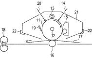
図1は、本発明に係る電子写真装置の一実施形態における構成例を示した概略図である。図1に示す電子写真装置の実施形態では、本発明の電子写真感光体を有するプロセスカートリッジを備える構成である。 FIG. 1 is a schematic view showing a configuration example in an embodiment of an electrophotographic apparatus according to the present invention. In the embodiment of the electrophotographic apparatus shown in FIG. 1, a process cartridge having the electrophotographic photosensitive member of the present invention is provided.
図1において、本発明の円筒状の電子写真感光体11は、軸12を中心に矢印方向(時計回り方向)に所定の周速度で回転駆動される。
回転駆動される電子写真感光体11の表面(周面)は、帯電手段13により正または負の電位に帯電され、次いで、画像露光手段(不図示)から出力される露光光(画像露光光)14を受ける。こうして電子写真感光体11の表面には、目的の画像に対応した静電潜像が形成されていく。
In FIG. 1, a cylindrical electrophotographic photosensitive member 11 of the present invention is driven to rotate at a predetermined peripheral speed in the direction of an arrow (clockwise direction) about a
The surface (circumferential surface) of the electrophotographic photosensitive member 11 that is driven to rotate is charged to a positive or negative potential by the charging
帯電手段13としては、例えば、コロトロン、スコロトロンなどを用いたコロナ帯電手段や、ローラー、ブラシ、フィルムなどを用いた接触帯電手段などが挙げられる。また、帯電手段に印加する電圧は、直流電圧のみであってもよいし、交流電圧を重畳した直流電圧であってもよい。
Examples of the charging
また、露光手段としては、例えば、スリット露光、レーザービーム走査露光などが挙げられる。 Examples of the exposure means include slit exposure and laser beam scanning exposure.
電子写真感光体11の表面に形成された静電潜像は、現像手段15中に収容されているトナーを用いて現像手段15により現像されてトナー画像となる。現像方式としては、磁性あるいは非磁性の一成分または二成分の現像剤を(一成分現像剤であるトナーを、または二成分現像剤であるトナーおよびキャリアを)用いて、接触させてまたは非接触で現像する方式が挙げられる。
The electrostatic latent image formed on the surface of the electrophotographic photosensitive member 11 is developed by the developing
トナーとしては、例えば、懸濁重合、乳化重合などによる重合トナーや、機械式粉砕法や球形化処理などによって球形化されたトナーなどが挙げられる。トナーの重量平均粒径は4〜7μmであることが好ましく、トナーの平均円形度は0.95〜0.99であることが好ましい。 Examples of the toner include polymerized toner by suspension polymerization, emulsion polymerization, and the like, and toner that has been spheroidized by a mechanical pulverization method or spheronization treatment. The weight average particle diameter of the toner is preferably 4 to 7 μm, and the average circularity of the toner is preferably 0.95 to 0.99.
電子写真感光体11の表面に形成されたトナー画像は、転写手段16によって、転写材(紙など)17に順次転写されていく。転写材17は、転写材供給手段(不図示)から電子写真感光体11と転写手段16との間(当接部)に電子写真感光体11の回転と同期して取り出されて給送される。
The toner image formed on the surface of the electrophotographic photoreceptor 11 is sequentially transferred onto a transfer material (paper or the like) 17 by the
トナー画像が転写された転写材17は、電子写真感光体11の表面から分離されて定着手段18へ導入されて像定着を受けることにより、画像形成物(プリント、コピー)として電子写真装置外へプリントアウトされる。
The
トナー画像転写後の電子写真感光体11の表面は、クリーニング手段であるクリーニングブレード19が所定の線圧をもって電子写真感光体11の表面に当接しながら、当該電子写真感光体11の回転に伴い転写残トナーを除去する。しかる後に、電子写真感光体11は前露光手段(不図示)からの前露光光20により除電処理され、繰り返し画像形成に使用される。
The surface of the electrophotographic photosensitive member 11 after the transfer of the toner image is transferred along with the rotation of the electrophotographic photosensitive member 11 while a
上述の電子写真感光体11、帯電手段13、現像手段15、転写手段16、クリーニング手段であるクリーニングブレード19などから選択される構成要素のうち、電子写真感光体11を含む複数のものを容器に納めてプロセスカートリッジとして一体に結合して構成し、このプロセスカートリッジを電子写真装置本体に対して着脱自在に構成してもよい。図1では、電子写真感光体11と、帯電手段13と、現像手段15と、クリーニング手段であるクリーニングブレード19と、を一体に支持してカートリッジ化して、電子写真装置本体に設けられたレールなどの案内手段22を用いて電子写真装置本体に着脱自在なプロセスカートリッジ21としている。
Among the components selected from the above-described electrophotographic photosensitive member 11, charging
以下に、具体的な実施例を挙げて本発明をさらに詳細に説明する。ただし、本発明はこれらに限定されるものではない。実施例中の「部」は質量部を意味する。 Hereinafter, the present invention will be described in more detail with reference to specific examples. However, the present invention is not limited to these. “Parts” in the examples means parts by mass.
(実施例1)
直径30mm、長さ260mmのアルミニウムシリンダーを支持体とした。
次に、10質量%の酸化アンチモンを含有する酸化スズで被覆されている酸化チタン粒子50部、レゾール型フェノール樹脂25部、メトキシプロパノール30部、メタノール30部、および、シリコーンオイル(ポリジメチルシロキサンポリオキシアルキレン共重合体、重量平均分子量:3000)0.002部を、直径1mmのガラスビーズを用いたサンドミルに入れ、2時間分散処理することによって、導電層用塗布液を調製した。この導電層用塗布液を支持体上に浸漬塗布し、得られた塗膜を20分間140℃で硬化させることによって、膜厚が20μmの導電層を形成した。
Example 1
An aluminum cylinder having a diameter of 30 mm and a length of 260 mm was used as a support.
Next, 50 parts of titanium oxide particles coated with tin oxide containing 10% by weight of antimony oxide, 25 parts of a resol type phenol resin, 30 parts of methoxypropanol, 30 parts of methanol, and silicone oil (polydimethylsiloxane poly) A conductive layer coating solution was prepared by placing 0.002 part of an oxyalkylene copolymer (weight average molecular weight: 3000) in a sand mill using glass beads having a diameter of 1 mm and dispersing the mixture for 2 hours. This conductive layer coating solution was dip-coated on a support, and the resulting coating film was cured at 140 ° C. for 20 minutes to form a conductive layer having a thickness of 20 μm.
次に、N−メトキシメチル化6ナイロン5部をメタノール95部に溶解させることによって、下引き層用塗布液を調製した。この下引き層用塗布液を支持体上に浸漬塗布し、得られた塗膜を20分間100℃で乾燥させることによって、膜厚が0.5μmの下引き層を形成した。 Next, an undercoat layer coating solution was prepared by dissolving 5 parts of N-methoxymethylated 6 nylon in 95 parts of methanol. The undercoat layer coating solution was dip-coated on a support, and the resulting coating film was dried at 100 ° C. for 20 minutes to form an undercoat layer having a thickness of 0.5 μm.
次に、CuKα特性X線回折におけるブラッグ角(2θ±0.2°)の7.5°、9.9°、12.5°、16.3°、18.6°、25.1°および28.3°に強いピークを有する結晶形のヒドロキシガリウムフタロシアニン結晶(電荷発生物質)10部、下記
構造式(1)で示される化合物0.1部、
次に、下記構造式(2)で示される化合物(電荷輸送物質)40部、
一方、テトラヒドロフラン100部、および、六方晶窒化ホウ素粒子(GI=3.3、電気化学工業社製)33部、直径1mmのガラスビーズをペイントシェーカーに入れ、1時間分散処理することによって、六方晶窒化ホウ素分散液を得た。 On the other hand, 100 parts of tetrahydrofuran, 33 parts of hexagonal boron nitride particles (GI = 3.3, manufactured by Denki Kagaku Kogyo Co., Ltd.), glass beads having a diameter of 1 mm were placed in a paint shaker and dispersed for 1 hour, thereby producing hexagonal crystals. A boron nitride dispersion was obtained.
得られた電荷輸送物質溶解液および六方晶窒化ホウ素分散液を、乾燥後の電荷輸送層中における六方晶窒化ホウ素の体積分率が5体積%になるように混合・撹拌することによって、電荷輸送層用塗布液を調製した。この電荷輸送層塗布液を電荷発生層上に浸漬塗布し、得られた塗膜を1時間120℃で乾燥させることによって、膜厚が20μmの電荷輸送層(最表面層)を形成した。
これを実施例1の電子写真感光体とした。
The resulting charge transport material solution and hexagonal boron nitride dispersion were mixed and stirred so that the volume fraction of hexagonal boron nitride in the charge transport layer after drying was 5% by volume. A layer coating solution was prepared. The charge transport layer coating solution was dip-coated on the charge generation layer, and the resulting coating film was dried at 120 ° C. for 1 hour to form a charge transport layer (outermost surface layer) having a thickness of 20 μm.
This was designated as the electrophotographic photosensitive member of Example 1.
(実施例2)
GI値の異なる六方晶窒化ホウ素(GI=4.0、電気化学工業社製)を用いた以外は実施例1と同様の方法で電子写真感光体を作製した。乾燥後の電荷輸送層の膜厚は21μmであった。
(Example 2)
An electrophotographic photosensitive member was produced in the same manner as in Example 1 except that hexagonal boron nitride having a different GI value (GI = 4.0, manufactured by Denki Kagaku Kogyo Co., Ltd.) was used. The thickness of the charge transport layer after drying was 21 μm.
(実施例3)
GI値の異なる六方晶窒化ホウ素(GI=7.5、電気化学工業社製)を用いた以外は実施例1と同様の方法で電子写真感光体を作製した。乾燥後の電荷輸送層の膜厚は20μmであった。
(Example 3)
An electrophotographic photosensitive member was produced in the same manner as in Example 1 except that hexagonal boron nitride having a different GI value (GI = 7.5, manufactured by Denki Kagaku Kogyo Co., Ltd.) was used. The thickness of the charge transport layer after drying was 20 μm.
(実施例4)
GI値の異なる六方晶窒化ホウ素(GI=10.8、電気化学工業社製)を用いた以外は実施例1と同様の方法で電子写真感光体を作製した。乾燥後の電荷輸送層の膜厚は20μmであった。
(Example 4)
An electrophotographic photoreceptor was produced in the same manner as in Example 1 except that hexagonal boron nitride having a different GI value (GI = 10.8, manufactured by Denki Kagaku Kogyo Co., Ltd.) was used. The thickness of the charge transport layer after drying was 20 μm.
(実施例5)
GI値の異なる六方晶窒化ホウ素(GI=14.0、電気化学工業社製)を用いた以外は実施例1と同様の方法で電子写真感光体を作製した。乾燥後の電荷輸送層の膜厚は21μmであった。
(Example 5)
An electrophotographic photoreceptor was produced in the same manner as in Example 1 except that hexagonal boron nitride having a different GI value (GI = 14.0, manufactured by Denki Kagaku Kogyo Co., Ltd.) was used. The thickness of the charge transport layer after drying was 21 μm.
(実施例6)
乾燥後の電荷輸送層中における六方晶窒化ホウ素の体積分率が10体積%になるよう混合・撹拌した以外は実施例3と同様の方法で電子写真感光体を作製した。乾燥後の電荷輸送層の膜厚は21μmであった。
(Example 6)
An electrophotographic photosensitive member was produced in the same manner as in Example 3 except that mixing and stirring were performed so that the volume fraction of hexagonal boron nitride in the charge transport layer after drying was 10% by volume. The thickness of the charge transport layer after drying was 21 μm.
(実施例7)
乾燥後の電荷輸送層中における六方晶窒化ホウ素の体積分率が15体積%になるよう混合・撹拌した以外は実施例3と同様の方法で電子写真感光体を作製した。乾燥後の電荷輸送層の膜厚は21μmであった。
(Example 7)
An electrophotographic photosensitive member was produced in the same manner as in Example 3 except that mixing and stirring were performed so that the volume fraction of hexagonal boron nitride in the charge transport layer after drying was 15% by volume. The thickness of the charge transport layer after drying was 21 μm.
(参考例8)
乾燥後の電荷輸送層中における六方晶窒化ホウ素の体積分率が25体積%になるよう混合・撹拌した以外は実施例3と同様の方法で電子写真感光体を作製した。乾燥後の電荷輸送層の膜厚は21μmであった。
( Reference Example 8)
An electrophotographic photosensitive member was produced in the same manner as in Example 3 except that mixing and stirring were performed so that the volume fraction of hexagonal boron nitride in the charge transport layer after drying was 25% by volume. The thickness of the charge transport layer after drying was 21 μm.
(実施例9)
実施例1と同様にして電荷発生層まで形成した。
次に、構造式(2)で示される化合物(電荷輸送物質)40部、構造式(3)で示される化合物(電荷輸送物質)5部、および、構造式(4)で示される構成単位を有するポリアリレート(重量平均分子量:115000、テレフタル酸骨格とイソフタル酸骨格のモル比:テレフタル酸骨格/イソフタル酸骨格=50/50)50部を、モノクロロベンゼン300部に溶解させることによって、電荷輸送物質溶解液を得た。この電荷輸送物質溶解液を本実施例における電荷輸送層塗布液として、浸漬塗布により電荷発生層上に積層した。この電荷輸送層の膜厚は20μmであった。
Example 9
The charge generation layer was formed in the same manner as in Example 1.
Next, 40 parts of the compound represented by the structural formula (2) (charge transporting substance), 5 parts of the compound represented by the structural formula (3) (charge transporting substance), and the structural unit represented by the structural formula (4) 50 parts of polyarylate (weight average molecular weight: 115000, molar ratio of terephthalic acid skeleton to isophthalic acid skeleton: terephthalic acid skeleton / isophthalic acid skeleton = 50/50) is dissolved in 300 parts of monochlorobenzene, thereby dissolving the charge transport material. A solution was obtained. This charge transport material solution was laminated on the charge generation layer by dip coating as a charge transport layer coating solution in this example. The thickness of this charge transport layer was 20 μm.
次に、六方晶窒化ホウ素(GI=7.5、電気化学工業製)10部、下記構造式(5)で示される化合物(メタクリル樹脂のモノマー)47部、及びエタノール143部をペイントシェーカーに入れ、2時間分散処理することにより、保護層用塗布液を調製した。
(実施例10)
六方晶窒化ホウ素(GI=7.5、電気化学工業社製)5部を水/エタノール=1/9の混合溶剤9部に加えた。そこに、シランカップリング剤としてオクタデシルトリメトキシシラン(東京化成製)を0.1部加え、少量の酢酸を滴下した後、直径1mmのジルコニアビーズを加え、ペイントシェーカーで3時間撹拌した。その後、反応溶液をトルエンで3回洗浄し、170℃で1時間乾燥し、シランカップリング処理した六方晶窒化ホウ素を得た。
次に、上記で得られた六方晶窒化ホウ素を用いた以外は、実施例3と同様の方法で電子写真感光体を作製した。乾燥後の電荷輸送層の膜厚は21μmであった。
(Example 10)
5 parts of hexagonal boron nitride (GI = 7.5, manufactured by Denki Kagaku Kogyo Co., Ltd.) was added to 9 parts of a mixed solvent of water / ethanol = 1/9. Thereto, 0.1 part of octadecyltrimethoxysilane (manufactured by Tokyo Chemical Industry Co., Ltd.) was added as a silane coupling agent, a small amount of acetic acid was added dropwise, zirconia beads having a diameter of 1 mm were added, and the mixture was stirred with a paint shaker for 3 hours. Thereafter, the reaction solution was washed three times with toluene, dried at 170 ° C. for 1 hour, and hexagonal boron nitride treated with silane coupling was obtained.
Next, an electrophotographic photosensitive member was produced in the same manner as in Example 3 except that the hexagonal boron nitride obtained above was used. The thickness of the charge transport layer after drying was 21 μm.
(実施例11)
シランカップリング剤としてn−デシルトリエトキシシラン(東京化成製)を用いた以外は、実施例10と同様の方法で電子写真感光体を作製した。乾燥後の電荷輸送層の膜厚は20μmであった。
(Example 11)
An electrophotographic photoreceptor was produced in the same manner as in Example 10 except that n-decyltriethoxysilane (manufactured by Tokyo Chemical Industry) was used as the silane coupling agent. The thickness of the charge transport layer after drying was 20 μm.
(実施例12)
シランカップリング剤として、トリメトキシ(1H、1H、2H、2H−ヘプタデカフルオロデシル)シラン(東京化成製)を用いた以外は、実施例10と同様の方法で電子写真感光体を作製した。乾燥後の電荷輸送層の膜厚は20μmであった。
Example 12
An electrophotographic photosensitive member was produced in the same manner as in Example 10 except that trimethoxy (1H, 1H, 2H, 2H-heptadecafluorodecyl) silane (manufactured by Tokyo Chemical Industry) was used as the silane coupling agent. The thickness of the charge transport layer after drying was 20 μm.
(比較例1)
GI値の異なる六方晶窒化ホウ素(GI=0.9、電気化学工業社製)を用いた以外は実施例1と同様の方法で、最面表層を電荷輸送層とする電子写真感光体を作製した。乾燥後の電荷輸送層の膜厚は20μmであった。
(Comparative Example 1)
An electrophotographic photosensitive member having the outermost surface layer as a charge transport layer was prepared in the same manner as in Example 1 except that hexagonal boron nitride having a different GI value (GI = 0.9, manufactured by Denki Kagaku Kogyo Co., Ltd.) was used. did. The thickness of the charge transport layer after drying was 20 μm.
(比較例2)
GI値の異なる六方晶窒化ホウ素(GI=1.5、電気化学工業社製)を用いた以外は実施例1と同様の方法で、最表面層を電荷輸送層とする電子写真感光体を作製した。乾燥後の電荷輸送層の膜厚は20μmであった。
(Comparative Example 2)
An electrophotographic photosensitive member having an outermost surface layer as a charge transport layer is prepared in the same manner as in Example 1 except that hexagonal boron nitride having a different GI value (GI = 1.5, manufactured by Denki Kagaku Kogyo Co., Ltd.) is used. did. The thickness of the charge transport layer after drying was 20 μm.
(比較例3)
GI値の異なる六方晶窒化ホウ素(GI=2.8、電気化学工業社製)を用いた以外は実施例1と同様の方法で、最表面層を電荷輸送層とする電子写真感光体を作製した。乾燥後の電荷輸送層の膜厚は20μmであった。
(Comparative Example 3)
An electrophotographic photosensitive member having the outermost surface layer as a charge transport layer is produced in the same manner as in Example 1 except that hexagonal boron nitride having a different GI value (GI = 2.8, manufactured by Denki Kagaku Kogyo Co., Ltd.) is used. did. The thickness of the charge transport layer after drying was 20 μm.
(比較例4)
GI値の異なる六方晶窒化ホウ素(GI=15.2、電気化学工業社製)を用いた以外は実施例1と同様の方法で、最表面層を電荷輸送層とする電子写真感光体を作製した。乾燥後の電荷輸送層の膜厚は20μmであった。
(Comparative Example 4)
An electrophotographic photoreceptor having the outermost surface layer as a charge transport layer is prepared in the same manner as in Example 1 except that hexagonal boron nitride having a different GI value (GI = 15.2, manufactured by Denki Kagaku Kogyo Co., Ltd.) is used. did. The thickness of the charge transport layer after drying was 20 μm.
(比較例5)
電荷発生層までは、実施例1と同様に作成した。
次に、ポリテトラフルオロエチレン(PTFE)粉末(ルブロンL−2、ダイキン工業製)100部、界面活性剤(GF−300、東亜合成製)5部、トルエン315部、1mm径ガラスビーズをペイントシェーカーに入れ、1時間分散処理し、PTFE分散液を作製した。次いで、実施例1に記載の電荷輸送物質溶解液と、作製したPTFE分散液とを、乾燥後における電荷輸送層のPTFE含有量が5体積%になるよう混合・撹拌し、電荷輸送層用塗布液を調製した。この電荷輸送層塗布液を電荷発生層上に浸漬塗布し、得られた塗膜を1時間120℃で乾燥させることによって、20μmの電荷輸送層(最表面層)を形成し、電子写真感光体を作製した。
(Comparative Example 5)
The charge generation layer was made in the same manner as in Example 1.
Next, 100 parts of polytetrafluoroethylene (PTFE) powder (Lublon L-2, manufactured by Daikin Industries), 5 parts of a surfactant (GF-300, manufactured by Toagosei Co., Ltd.), 315 parts of toluene, 1 mm diameter glass beads, paint shaker And dispersed for 1 hour to prepare a PTFE dispersion. Next, the charge transport material solution described in Example 1 and the prepared PTFE dispersion were mixed and stirred so that the PTFE content of the charge transport layer after drying was 5% by volume, and applied to the charge transport layer. A liquid was prepared. This charge transport layer coating solution is dip coated on the charge generation layer, and the resulting coating film is dried at 120 ° C. for 1 hour to form a 20 μm charge transport layer (outermost surface layer). Was made.
(比較例6)
実施例1と同様にして電荷発生層まで形成した。
次に、実施例1に記載の電荷輸送物質溶解液を本比較例における電荷輸送層塗布液として電荷発生層上に浸漬塗布し、得られた塗膜を1時間120℃で乾燥させることによって、20μmの電荷輸送層を形成した。続いて、六方晶窒化ホウ素(GI=7.5、電気化学工業社製)5部、エタノール95部、1mm径のガラスビーズをペイントシェーカーに入れ、1時間分散処理し、六方晶窒化ホウ素分散液を作製した。この六方晶窒化ホウ素分散液を電荷輸送層上に浸漬塗布し、得られた塗膜を10分、120℃で乾燥させ、電子写真感光体を作製した。
(Comparative Example 6)
The charge generation layer was formed in the same manner as in Example 1.
Next, by dip-coating the charge transport material solution described in Example 1 onto the charge generation layer as the charge transport layer coating solution in this comparative example, and drying the obtained coating film at 120 ° C. for 1 hour, A 20 μm charge transport layer was formed. Subsequently, 5 parts of hexagonal boron nitride (GI = 7.5, manufactured by Denki Kagaku Kogyo Co., Ltd.), 95 parts of ethanol, and 1 mm diameter glass beads were placed in a paint shaker and dispersed for 1 hour to obtain a hexagonal boron nitride dispersion. Was made. This hexagonal boron nitride dispersion was dip-coated on the charge transport layer, and the resulting coating film was dried at 120 ° C. for 10 minutes to produce an electrophotographic photoreceptor.
(比較例7)
窒化ホウ素として、立方晶窒化ホウ素(昭和電工製)を用いた以外は、実施例6と同様の方法で、最表面層を電荷輸送層とする電子写真感光体を作製した。乾燥後の電荷輸送層の膜厚は20μmであった。
(Comparative Example 7)
An electrophotographic photosensitive member having an outermost surface layer as a charge transport layer was produced in the same manner as in Example 6 except that cubic boron nitride (manufactured by Showa Denko) was used as boron nitride. The thickness of the charge transport layer after drying was 20 μm.
以上、作製した電子写真感光体の詳細を表1に示す。 The details of the produced electrophotographic photosensitive member are shown in Table 1.
(評価方法)
(ブレード鳴き、捲れの評価)
評価は、まず、作製した電子写真感光体を、ヒューレットパッカード社製のレーザービームプリンター(LBP)(商品名:レーザージェット4300n(モノクロ機))用のプロセスカートリッジに装着した。このLBPにて2000枚の画像出力(耐久試験)を行って、最初の5枚(初期)と最後の5枚(耐久試験後半)の段階でブレード捲れやブレード鳴きの有無を評価した。
(Evaluation methods)
(Evaluation of blade noise and drowning)
In the evaluation, first, the produced electrophotographic photosensitive member was mounted on a process cartridge for a laser beam printer (LBP) (trade name: Laser Jet 4300n (monochrome machine)) manufactured by Hewlett-Packard Company. With this LBP, 2000 images were output (endurance test), and the presence or absence of blade squeezing or blade squealing was evaluated at the first 5 sheets (initial stage) and the last 5 sheets (second half of the endurance test).
(動摩擦係数の測定)
動摩擦係数の測定は、JIS−A硬度が70度であるウレタンブレードと電子写真感光体との動摩擦係数の変化を測定した。上記ブレード鳴き、捲れの評価に用いた、初期連続2,000枚通紙使用後の電子写真感光体を評価装置から取りだした。この電子写真感光体について、表面性測定機Type14FW(新東科学社製)を用いて垂直荷重30g、摺擦速度100mm/minの条件で、図2に示すようにウレタンブレード32を電子写真感光体31の表面に対して当接角26°および当接圧30gとなるように設定し、動摩擦係数を測定した。なお、電子写真感光体31は留め具33で固定されている。
得られた動摩擦係数を通紙時(耐久使用時)の動摩擦係数とした。また、上記ブレード鳴き、捲れの評価を行う前にあらかじめ測定しておいたウレタンブレード32の動摩擦係数を初期の動摩擦係数とした。
なお、図2中、実線矢印(垂直下向きの矢印)はウレタンブレード32にかかる垂直荷重を示し、破線矢印(水平左向きの矢印)はウレタンブレード32の移動方向を示す。
(Measurement of dynamic friction coefficient)
The dynamic friction coefficient was measured by measuring the change in the dynamic friction coefficient between the urethane blade having a JIS-A hardness of 70 degrees and the electrophotographic photosensitive member. The electrophotographic photosensitive member after the initial continuous use of 2,000 sheets, which was used for the evaluation of the blade squeal and wrinkle, was taken out from the evaluation apparatus. With respect to this electrophotographic photosensitive member, the
The obtained dynamic friction coefficient was defined as the dynamic friction coefficient during paper passing (during durable use). In addition, the dynamic friction coefficient of the
In FIG. 2, a solid line arrow (vertical downward arrow) indicates a vertical load applied to the
(電位特性)
ドラム電子写真感光体試験装置(ジェンテック社製「CYNTHIA59」)を用い、23℃/50%RHの環境下で電子写真特性を測定した。
測定方法は、ドラム状の電子写真感光体を暗所下60rpmで回転させながら、コロナ放電により負帯電させ、電位プローブ位置での電位V0が−700Vになるように一次電流を制御した。ここで、光源としてハロゲンランプを用い、フィルターで単色光(775nm)としたものを照射し、表面電位がV0の1/2(すなわち、−350V)に減少するまでの露光量を求め、その半減露光量E1/2[μJ/cm2]を感度とした。更に、帯電/露光後に波長700nmの発光ダイオードにより15μJ/cm2のエネルギーを与えて除電する前露光工程を入れ、前露光工程における露光の終了後、0.3秒経過時の電位を残留電位(Vr)[−V]とした。
(Potential characteristics)
The electrophotographic characteristics were measured in a 23 ° C./50% RH environment using a drum electrophotographic photoreceptor test apparatus (“CYNTHIA59” manufactured by Gentec).
In the measurement method, the drum-shaped electrophotographic photosensitive member was rotated at 60 rpm in the dark while being negatively charged by corona discharge, and the primary current was controlled so that the potential V 0 at the potential probe position was −700 V. Here, a halogen lamp is used as the light source, and the filter is irradiated with monochromatic light (775 nm), and the exposure amount until the surface potential is reduced to 1/2 of V 0 (ie, −350 V) is obtained. The half exposure amount E 1/2 [μJ / cm 2 ] was defined as sensitivity. Further, after the charging / exposure, a pre-exposure step is performed in which a light-emitting diode having a wavelength of 700 nm is applied to remove electricity by applying energy of 15 μJ / cm 2. Vr) [-V].
以上の評価結果を表1に示す。 The above evaluation results are shown in Table 1.
表1より、六方晶窒化ホウ素は、その結晶化度に応じて動摩擦係数が変化し、GIが3.0以上になると動摩擦係数が大きく低下し、電子写真プロセスの耐久使用に渡って動摩擦係数の変化が小さいことがわかった。また、六方晶窒化ホウ素を分散した膜はPTFEを同量含有する膜に比べて動摩擦係数が低く、電気的な劣化に対する耐性(耐久使用)に優れることもわかり、従来の材料に優位性を持つことがわかった。また、六方晶窒化ホウ素を分散した膜は、電子写真感光体に外部から塗布した(塗膜を形成した)場合に比べて、動摩擦係数が小さくなることもわかった。
さらに、シランカップリング剤で表面処理した窒化ホウ素を用いた場合、電位特性が向上することがわかった。
From Table 1, the hexagonal boron nitride has a dynamic friction coefficient that changes depending on the degree of crystallinity. When the GI is 3.0 or more, the dynamic friction coefficient is greatly reduced. I found that the change was small. Also, it can be seen that a film in which hexagonal boron nitride is dispersed has a lower coefficient of dynamic friction than a film containing the same amount of PTFE, and has superior resistance to electrical deterioration (durable use), and has an advantage over conventional materials. I understood it. It has also been found that the film in which hexagonal boron nitride is dispersed has a smaller coefficient of dynamic friction than when the film is applied to the electrophotographic photosensitive member from the outside (a coating film is formed).
Furthermore, it was found that the potential characteristics were improved when boron nitride surface-treated with a silane coupling agent was used.
11 電子写真感光体
12 軸
13 帯電手段
14 露光光(画像露光光)
15 現像手段
16 転写手段
17 転写材
18 定着手段
19 クリーニングブレード
20 前露光光
21 プロセスカートリッジ
22 案内手段
11 Electrophotographic
15 Developing means 16 Transfer means 17
Claims (6)
前記電子写真感光体の最表面層が結着樹脂を含有し、
前記最表面層の結着樹脂に六方晶窒化ホウ素が分散されており、かつ、前記六方晶窒化ホウ素の黒鉛化指数(GI)が3.0以上15.0未満であり、および
前記六方晶窒化ホウ素の最表面層の体積に対する含有割合が1体積%〜20体積%であることを特徴とする電子写真感光体。 An electrophotographic photosensitive member having a support and a photosensitive layer provided on the support,
The outermost surface layer of the electrophotographic photoreceptor contains a binder resin;
It said being hexagonal boron nitride in the binder resin of the outermost layer is dispersed, and Ri graphitization index (GI) is 3.0 to 15.0 than der of the hexagonal boron nitride, and
Electrophotographic photoreceptor proportion to the volume of the outermost surface layer of said hexagonal boron nitride is characterized by 1 vol% to 20 vol% der Rukoto.
前記電子写真感光体の表面を帯電させる帯電手段、トナーを用いて前記電子写真感光体上に形成された静電潜像を現像してトナー画像を形成する現像手段、前記電子写真感光体上に形成された前記トナー画像を転写材に転写する転写手段、および前記電子写真感光体の表面に当接しながら当該電子写真感光体をクリーニングするクリーニングブレードを有するクリーニング手段からなる群より選択される少なくとも1つの手段と、を一体に支持し、電子写真装置本体に着脱自在であることを特徴とするプロセスカートリッジ。 An electrophotographic photosensitive member according to any one of claims 1 to 4 ,
A charging means for charging the surface of the electrophotographic photosensitive member, a developing means for developing a latent electrostatic image formed on the electrophotographic photosensitive member using toner and forming a toner image, on the electrophotographic photosensitive member At least one selected from the group consisting of transfer means for transferring the formed toner image to a transfer material, and cleaning means having a cleaning blade for cleaning the electrophotographic photosensitive member while contacting the surface of the electrophotographic photosensitive member. And a detachable attachment to the main body of the electrophotographic apparatus.
前記電子写真感光体の表面を帯電させる帯電手段と、
帯電された前記電子写真感光体を露光して静電潜像を形成する画像露光手段と、
トナーを用いて前記電子写真感光体上に形成された前記静電潜像を現像してトナー画像を形成する現像手段と、
前記電子写真感光体上に形成された前記トナー画像を転写材に転写する転写手段と、
前記電子写真感光体の表面に当接しながら当該電子写真感光体をクリーニングするクリーニングブレードを有するクリーニング手段と、を有することを特徴とする電子写真装置。 An electrophotographic photosensitive member according to any one of claims 1 to 4 ,
Charging means for charging the surface of the electrophotographic photosensitive member;
Image exposing means for exposing the charged electrophotographic photosensitive member to form an electrostatic latent image; and
Developing means for developing the electrostatic latent image formed on the electrophotographic photoreceptor using toner to form a toner image;
Transfer means for transferring the toner image formed on the electrophotographic photosensitive member to a transfer material;
An electrophotographic apparatus comprising: a cleaning unit having a cleaning blade for cleaning the electrophotographic photosensitive member while being in contact with the surface of the electrophotographic photosensitive member.
Priority Applications (3)
| Application Number | Priority Date | Filing Date | Title |
|---|---|---|---|
| JP2015094849A JP6588731B2 (en) | 2015-05-07 | 2015-05-07 | Electrophotographic photosensitive member, process cartridge, and electrophotographic apparatus |
| US15/132,227 US9791792B2 (en) | 2015-05-07 | 2016-04-18 | Electrophotographic photosensitive member, process cartridge and electrophotographic apparatus |
| DE102016108275.9A DE102016108275B4 (en) | 2015-05-07 | 2016-05-04 | ELECTROPHOTOGRAPHIC LIGHT SENSITIVE ELEMENT, PROCESS CARTRIDGE AND ELECTROPHOTOGRAPHIC DEVICE |
Applications Claiming Priority (1)
| Application Number | Priority Date | Filing Date | Title |
|---|---|---|---|
| JP2015094849A JP6588731B2 (en) | 2015-05-07 | 2015-05-07 | Electrophotographic photosensitive member, process cartridge, and electrophotographic apparatus |
Publications (3)
| Publication Number | Publication Date |
|---|---|
| JP2016212218A JP2016212218A (en) | 2016-12-15 |
| JP2016212218A5 JP2016212218A5 (en) | 2018-06-14 |
| JP6588731B2 true JP6588731B2 (en) | 2019-10-09 |
Family
ID=57179101
Family Applications (1)
| Application Number | Title | Priority Date | Filing Date |
|---|---|---|---|
| JP2015094849A Active JP6588731B2 (en) | 2015-05-07 | 2015-05-07 | Electrophotographic photosensitive member, process cartridge, and electrophotographic apparatus |
Country Status (3)
| Country | Link |
|---|---|
| US (1) | US9791792B2 (en) |
| JP (1) | JP6588731B2 (en) |
| DE (1) | DE102016108275B4 (en) |
Families Citing this family (29)
| Publication number | Priority date | Publication date | Assignee | Title |
|---|---|---|---|---|
| JP2016038577A (en) | 2014-08-06 | 2016-03-22 | キヤノン株式会社 | Electrophotographic photoreceptor, process cartridge and electrophotographing device |
| EP3201691B1 (en) | 2014-09-30 | 2019-04-24 | Canon Kabushiki Kaisha | Electrophotographic photosensitive member, process cartridge and electrophotographic apparatus |
| US9811012B2 (en) | 2015-09-24 | 2017-11-07 | Canon Kabushiki Kaisha | Electrophotographic photosensitive member, process cartridge, electrophotographic apparatus and process for producing electrophotographic photosensitive member |
| JP6704739B2 (en) | 2016-01-28 | 2020-06-03 | キヤノン株式会社 | Electrophotographic photoreceptor, process cartridge and electrophotographic apparatus |
| JP6639256B2 (en) | 2016-02-10 | 2020-02-05 | キヤノン株式会社 | Electrophotographic apparatus and process cartridge |
| US9983490B2 (en) | 2016-03-31 | 2018-05-29 | Canon Kabushiki Kaisha | Electrophotographic apparatus |
| JP7060921B2 (en) | 2017-04-18 | 2022-04-27 | キヤノン株式会社 | Electrophotographic photosensitive members, process cartridges and electrophotographic equipment |
| US10241429B2 (en) | 2017-04-27 | 2019-03-26 | Canon Kabushiki Kaisha | Electrophotographic photosensitive member, process cartridge and electrophotographic apparatus |
| JP6983543B2 (en) | 2017-06-09 | 2021-12-17 | キヤノン株式会社 | Electrophotographic photosensitive members, process cartridges and electrophotographic equipment |
| JP6918663B2 (en) | 2017-09-26 | 2021-08-11 | キヤノン株式会社 | Electrophotographic photosensitive members, process cartridges and electrophotographic equipment |
| JP7034655B2 (en) | 2017-10-03 | 2022-03-14 | キヤノン株式会社 | Electrophotographic photosensitive members, process cartridges and electrophotographic equipment |
| JP7057104B2 (en) | 2017-11-24 | 2022-04-19 | キヤノン株式会社 | Process cartridge and electrophotographic image forming apparatus |
| JP7187270B2 (en) | 2017-11-24 | 2022-12-12 | キヤノン株式会社 | Process cartridge and electrophotographic device |
| JP7046571B2 (en) | 2017-11-24 | 2022-04-04 | キヤノン株式会社 | Process cartridges and electrophotographic equipment |
| JP7034769B2 (en) | 2018-02-28 | 2022-03-14 | キヤノン株式会社 | Electrophotographic photosensitive members, process cartridges and electrophotographic equipment |
| JP7034768B2 (en) | 2018-02-28 | 2022-03-14 | キヤノン株式会社 | Process cartridge and image forming equipment |
| JP2019152699A (en) | 2018-02-28 | 2019-09-12 | キヤノン株式会社 | Electrophotographic photoreceptor, process cartridge, and electrophotographic device |
| JP7129225B2 (en) | 2018-05-31 | 2022-09-01 | キヤノン株式会社 | Electrophotographic photoreceptor and method for producing electrophotographic photoreceptor |
| JP7150485B2 (en) | 2018-05-31 | 2022-10-11 | キヤノン株式会社 | Electrophotographic photoreceptor, process cartridge and electrophotographic apparatus |
| JP7059112B2 (en) | 2018-05-31 | 2022-04-25 | キヤノン株式会社 | Electrophotographic photosensitive member, process cartridge and electrophotographic image forming apparatus |
| JP7054366B2 (en) | 2018-05-31 | 2022-04-13 | キヤノン株式会社 | Electrophotographic photosensitive members, process cartridges and electrophotographic equipment |
| US10747130B2 (en) | 2018-05-31 | 2020-08-18 | Canon Kabushiki Kaisha | Process cartridge and electrophotographic apparatus |
| JP7075288B2 (en) | 2018-06-05 | 2022-05-25 | キヤノン株式会社 | Electrophotographic photosensitive members, process cartridges and electrophotographic equipment |
| JP7413054B2 (en) | 2019-02-14 | 2024-01-15 | キヤノン株式会社 | Electrophotographic photoreceptors, process cartridges, and electrophotographic devices |
| US11320754B2 (en) | 2019-07-25 | 2022-05-03 | Canon Kabushiki Kaisha | Process cartridge and electrophotographic apparatus |
| US11573499B2 (en) | 2019-07-25 | 2023-02-07 | Canon Kabushiki Kaisha | Process cartridge and electrophotographic apparatus |
| JP7337652B2 (en) | 2019-10-18 | 2023-09-04 | キヤノン株式会社 | Process cartridge and electrophotographic apparatus using the same |
| JP7337649B2 (en) | 2019-10-18 | 2023-09-04 | キヤノン株式会社 | Process cartridge and electrophotographic device |
| US11372351B2 (en) | 2020-09-14 | 2022-06-28 | Canon Kabushiki Kaisha | Electrophotographic member and electrophotographic image forming apparatus |
Family Cites Families (94)
| Publication number | Priority date | Publication date | Assignee | Title |
|---|---|---|---|---|
| US4729937A (en) * | 1985-12-26 | 1988-03-08 | Kabushiki Kaisha Toshiba | Layered amorphous silicon electrophotographic photosensitive member comprises BN surface layer and BN barrier layer |
| US4845001A (en) * | 1986-04-30 | 1989-07-04 | Canon Kabushiki Kaisha | Light receiving member for use in electrophotography with a surface layer comprising non-single-crystal material containing tetrahedrally bonded boron nitride |
| US5124219A (en) * | 1989-03-15 | 1992-06-23 | Minolta Camera Kabushiki Kaisha | Photosensitive member for electrophotography comprising specified nylon copolymer |
| JPH07319182A (en) * | 1994-05-25 | 1995-12-08 | Mita Ind Co Ltd | Electrophotographic photoreceptor |
| JP3530676B2 (en) * | 1995-04-26 | 2004-05-24 | キヤノン株式会社 | Method for manufacturing light receiving member, light receiving member, electrophotographic apparatus having light receiving member, and electrophotographic process using light receiving member |
| JP3461651B2 (en) * | 1996-01-24 | 2003-10-27 | 電気化学工業株式会社 | Hexagonal boron nitride powder and its use |
| EP0798599B9 (en) | 1996-03-27 | 2002-08-07 | Canon Kabushiki Kaisha | Electrophotographic photosensitive member, and electrophotographic apparatus and process cartridge including same |
| US5876890A (en) | 1996-05-27 | 1999-03-02 | Canon Kabushiki Kaisha | Electrophotographic photosensitive member and apparatus and process cartridge provided with the same |
| JP3238634B2 (en) * | 1996-09-30 | 2001-12-17 | 電気化学工業株式会社 | Grease composition |
| JPH10102083A (en) * | 1996-10-01 | 1998-04-21 | Denki Kagaku Kogyo Kk | Lubricant |
| US6408152B1 (en) | 1998-04-30 | 2002-06-18 | Canon Kabushiki Kaisha | Process cartridge and electrophotographic apparatus |
| US6562530B2 (en) | 2000-06-21 | 2003-05-13 | Canon Kabushiki Kaisha | Electrophotographic photosensitive member, and process cartridge and electrophotographic apparatus having the electrophotographic photosensitive member |
| JP3766008B2 (en) * | 2000-11-30 | 2006-04-12 | 株式会社リコー | Electrophotographic photosensitive member, method for producing the same, electrophotographic method, image forming apparatus, and process cartridge for image forming apparatus |
| US6806009B2 (en) | 2001-12-21 | 2004-10-19 | Canon Kabushiki Kaisha | Electrophotographic photosensitive member, process cartridge and electrophotographic apparatus |
| MXPA02012321A (en) | 2001-12-21 | 2004-12-13 | Canon Kk | Electrophotographic photosensitive member, process cartridgeand electrophotographic apparatus. |
| US6913862B2 (en) | 2001-12-21 | 2005-07-05 | Canon Kabushiki Kaisha | Phenolic compound, novel resol resin, cured products thereof, electrophotographic photosensitive member containing them, and process cartridge and electrophotographic apparatus which have the electrophotographic photosensitive member |
| MXPA02012553A (en) | 2001-12-21 | 2004-09-03 | Canon Kk | Electrophotographic photosensitive member, process cartridge and electrophotographic apparatus. |
| JP2004004146A (en) | 2002-04-19 | 2004-01-08 | Canon Inc | Conductive member, processing cartridge, and image forming apparatus |
| DE60324219D1 (en) | 2002-04-26 | 2008-12-04 | Canon Kk | Electrophotographic photosensitive member, process cartridge and electrophotographic apparatus |
| US7022446B2 (en) | 2002-07-15 | 2006-04-04 | Canon Kk | Electrophotographic photosensitive member, process cartridge and electrophotographic apparatus |
| DE60318155T2 (en) | 2002-07-15 | 2008-12-11 | Canon K.K. | Electrophotographic photosensitive member, image recording apparatus, and process cartridge |
| JP4174391B2 (en) | 2002-08-30 | 2008-10-29 | キヤノン株式会社 | Electrophotographic photosensitive member, process cartridge, and electrophotographic apparatus |
| JP3913148B2 (en) | 2002-08-30 | 2007-05-09 | キヤノン株式会社 | Electrophotographic photosensitive member, process cartridge, and electrophotographic apparatus |
| US7001699B2 (en) | 2002-08-30 | 2006-02-21 | Canon Kabushiki Kaisha | Electrophotographic photosensitive member, process cartridge and electrophotographic apparatus |
| CN100373262C (en) | 2002-11-18 | 2008-03-05 | 佳能株式会社 | Electrophotographic photosensitive member, electrophotographic apparatus, and process cartridge |
| JP4141341B2 (en) * | 2003-07-28 | 2008-08-27 | 株式会社リコー | Electrophotographic photosensitive member, image forming apparatus, and process cartridge for image forming apparatus |
| US7585604B2 (en) | 2004-09-10 | 2009-09-08 | Canon Kabushiki Kaisha | Electrographic photosensitive member, process cartridge and electrophotographic apparatus |
| WO2006129879A1 (en) | 2005-06-02 | 2006-12-07 | Canon Kabushiki Kaisha | Electrophotographic photoreceptor, process cartridge, and electrophotographic apparatus |
| US20080277619A1 (en) * | 2005-12-09 | 2008-11-13 | Kazuaki Matsumoto | Thermoplastic Resin Composition with High Thermal Conductivity |
| JP4059518B2 (en) | 2006-01-31 | 2008-03-12 | キヤノン株式会社 | Method for producing electrophotographic photosensitive member |
| JP4101278B2 (en) | 2006-01-31 | 2008-06-18 | キヤノン株式会社 | Electrophotographic photosensitive member, process cartridge, and electrophotographic apparatus |
| JP4183267B2 (en) | 2006-01-31 | 2008-11-19 | キヤノン株式会社 | Electrophotographic photosensitive member, process cartridge, and electrophotographic apparatus |
| JP4194631B2 (en) | 2006-01-31 | 2008-12-10 | キヤノン株式会社 | Image forming method and electrophotographic apparatus using the image forming method |
| US8663665B2 (en) * | 2006-03-02 | 2014-03-04 | Momentive Performance Materials Inc. | Anti-chafing compositions comprising boron nitride |
| EP2071403B1 (en) | 2006-10-31 | 2013-01-16 | Canon Kabushiki Kaisha | Electrophotographic photosensitive body, method for producing electrophotographic photosensitive body, process cartridge, and electrophotographic device |
| EP2071404B1 (en) | 2006-10-31 | 2013-02-13 | Canon Kabushiki Kaisha | Electrophotographic photosensitive body, method for producing electrophotographic photosensitive body, process cartridge, and electrophotographic device |
| US7851113B2 (en) * | 2006-11-01 | 2010-12-14 | Xerox Corporation | Electrophotographic photoreceptors having reduced torque and improved mechanical robustness |
| JP4041921B1 (en) | 2007-01-26 | 2008-02-06 | キヤノン株式会社 | Electrophotographic photoreceptor manufacturing method |
| JP4018741B1 (en) | 2007-01-26 | 2007-12-05 | キヤノン株式会社 | Method for producing a solid having a concave shape on the surface |
| JP4909105B2 (en) * | 2007-02-02 | 2012-04-04 | 電気化学工業株式会社 | Boron nitride containing slurry |
| WO2008117806A1 (en) | 2007-03-27 | 2008-10-02 | Canon Kabushiki Kaisha | Electrophotographic photosensitive material, process cartridge and electrophotographic apparatus |
| JP4372213B2 (en) | 2007-03-28 | 2009-11-25 | キヤノン株式会社 | Electrophotographic photosensitive member, process cartridge, and electrophotographic apparatus |
| JP4235673B2 (en) | 2007-07-17 | 2009-03-11 | キヤノン株式会社 | Method for producing electrophotographic photosensitive member |
| JP5239531B2 (en) * | 2008-06-16 | 2013-07-17 | 株式会社リコー | Image carrier protecting agent, protective layer forming apparatus, image forming method, image forming apparatus, and process cartridge |
| KR101317070B1 (en) | 2008-07-18 | 2013-10-11 | 캐논 가부시끼가이샤 | Electrophotographic photoreceptor, process cartridge, and electrophotographic apparatus |
| CN102165375B (en) | 2008-09-26 | 2013-06-19 | 佳能株式会社 | Electrophotographic photosensitive member, process cartridge, and electrophotographic apparatus |
| JP5369908B2 (en) * | 2009-06-04 | 2013-12-18 | 株式会社リコー | Image carrier protecting agent, method for applying image carrier protecting agent, protective layer forming apparatus, method for producing image carrier protecting agent, image forming method, process cartridge, and image forming apparatus |
| JP4663819B1 (en) | 2009-08-31 | 2011-04-06 | キヤノン株式会社 | Electrophotographic equipment |
| JP5573472B2 (en) * | 2009-09-02 | 2014-08-20 | 株式会社リコー | Image carrier protective agent, protective agent supply device, process cartridge, and image forming apparatus |
| JP5521525B2 (en) * | 2009-12-11 | 2014-06-18 | 株式会社リコー | Electrophotographic photoreceptor and electrophotographic apparatus using the electrophotographic photoreceptor |
| JP5629588B2 (en) | 2010-01-15 | 2014-11-19 | キヤノン株式会社 | Electrophotographic photosensitive member, process cartridge, and electrophotographic apparatus |
| JP5430449B2 (en) * | 2010-03-05 | 2014-02-26 | 電気化学工業株式会社 | High thermal conductive filler |
| CN103109236B (en) | 2010-09-14 | 2015-03-25 | 佳能株式会社 | Electrophotographic photosensitive member, process cartridge, electrophotographic apparatus, and method of manufacturing electrophotographic photosensitive member |
| JP4948670B2 (en) | 2010-10-14 | 2012-06-06 | キヤノン株式会社 | Electrophotographic photosensitive member, process cartridge, electrophotographic apparatus, and method of manufacturing electrophotographic photosensitive member |
| JP5036901B1 (en) | 2010-10-29 | 2012-09-26 | キヤノン株式会社 | Electrophotographic photosensitive member, process cartridge, electrophotographic apparatus, and method of manufacturing electrophotographic photosensitive member |
| JP4959022B2 (en) | 2010-10-29 | 2012-06-20 | キヤノン株式会社 | Electrophotographic photosensitive member, process cartridge, and electrophotographic apparatus |
| JP4975185B1 (en) | 2010-11-26 | 2012-07-11 | キヤノン株式会社 | Method for forming uneven shape on surface of surface layer of cylindrical electrophotographic photoreceptor, and method for producing cylindrical electrophotographic photoreceptor having uneven surface formed on surface of surface layer |
| JP4959024B1 (en) | 2010-12-02 | 2012-06-20 | キヤノン株式会社 | Electrophotographic photosensitive member, process cartridge, electrophotographic apparatus, and method of manufacturing electrophotographic photosensitive member |
| JP5089816B2 (en) | 2011-04-12 | 2012-12-05 | キヤノン株式会社 | Electrophotographic photosensitive member, process cartridge, electrophotographic apparatus, and method of manufacturing electrophotographic photosensitive member |
| JP5089815B2 (en) | 2011-04-12 | 2012-12-05 | キヤノン株式会社 | Electrophotographic photosensitive member, process cartridge, electrophotographic apparatus, and method of manufacturing electrophotographic photosensitive member |
| CN103998506B (en) * | 2011-12-16 | 2016-08-24 | 提克纳有限责任公司 | Boracic nucleator for polyphenylene sulfide |
| JP6040018B2 (en) | 2011-12-22 | 2016-12-07 | キヤノン株式会社 | Method for producing electrophotographic photoreceptor, method for producing organic device, and emulsion for charge transport layer |
| JP6071509B2 (en) | 2011-12-22 | 2017-02-01 | キヤノン株式会社 | Method for producing electrophotographic photosensitive member |
| JP6049417B2 (en) | 2011-12-22 | 2016-12-21 | キヤノン株式会社 | Electrophotographic photoreceptor having charge transport layer and method for producing organic device |
| US9689074B2 (en) * | 2012-02-27 | 2017-06-27 | Momentive Performance Materials, Inc. | Low drag coating containing boron nitride powder |
| JP6105974B2 (en) | 2012-03-15 | 2017-03-29 | キヤノン株式会社 | Method for producing electrophotographic photoreceptor and emulsion for charge transport layer |
| JP6105973B2 (en) | 2012-03-22 | 2017-03-29 | キヤノン株式会社 | Method for producing electrophotographic photoreceptor, emulsion for charge transport layer |
| JP6015160B2 (en) * | 2012-06-22 | 2016-10-26 | 富士ゼロックス株式会社 | Electrophotographic photosensitive member, process cartridge, and image forming apparatus |
| JP6049329B2 (en) | 2012-06-29 | 2016-12-21 | キヤノン株式会社 | Electrophotographic photosensitive member, method for manufacturing electrophotographic photosensitive member, process cartridge, and electrophotographic apparatus |
| US9029054B2 (en) | 2012-06-29 | 2015-05-12 | Canon Kabushiki Kaisha | Electrophotographic photosensitive member, process cartridge, and electrophotographic apparatus |
| KR101599579B1 (en) | 2012-06-29 | 2016-03-03 | 캐논 가부시끼가이샤 | Electrophotographic photosensitive member, process cartridge, and electrophotographic apparatus |
| KR101599578B1 (en) | 2012-06-29 | 2016-03-03 | 캐논 가부시끼가이샤 | Electrophotographic photosensitive member, process cartridge, and electrophotographic apparatus |
| JP5983152B2 (en) * | 2012-07-27 | 2016-08-31 | 株式会社リコー | Image forming apparatus |
| US20140077125A1 (en) * | 2012-09-19 | 2014-03-20 | Kang Yi Lin | Composition comprising exfoliated boron nitride and method for forming such compositions |
| JP5911459B2 (en) | 2012-09-28 | 2016-04-27 | キヤノン株式会社 | Electrophotographic photosensitive member, manufacturing method thereof, process cartridge, and electrophotographic apparatus |
| JP6028501B2 (en) * | 2012-10-03 | 2016-11-16 | 株式会社リコー | Image carrier protecting agent, protective layer forming apparatus, and image forming apparatus |
| JP6198571B2 (en) | 2012-11-30 | 2017-09-20 | キヤノン株式会社 | Electrophotographic photosensitive member, method for manufacturing electrophotographic photosensitive member, process cartridge, and electrophotographic apparatus |
| JP2014130329A (en) | 2012-11-30 | 2014-07-10 | Canon Inc | Electrophotographic photoreceptor, method for manufacturing electrophotographic photoreceptor, process cartridge, and electrophotographic device |
| JP2014119508A (en) | 2012-12-13 | 2014-06-30 | Ricoh Co Ltd | Image forming apparatus and process cartridge |
| JP6218006B2 (en) * | 2012-12-17 | 2017-10-25 | 株式会社リコー | Electrophotographic photoreceptor |
| WO2014136959A1 (en) * | 2013-03-07 | 2014-09-12 | 電気化学工業株式会社 | Boron-nitride powder and resin composition containing same |
| US10301328B2 (en) * | 2013-03-25 | 2019-05-28 | Jiasheng Lu | Organoboron compounds and methods of making same |
| JP6161425B2 (en) | 2013-06-19 | 2017-07-12 | キヤノン株式会社 | Method for producing electrophotographic photosensitive member |
| JP6353285B2 (en) | 2013-06-19 | 2018-07-04 | キヤノン株式会社 | Method for producing electrophotographic photosensitive member |
| JP6423697B2 (en) | 2013-12-26 | 2018-11-14 | キヤノン株式会社 | Electrophotographic photosensitive member, method for manufacturing electrophotographic photosensitive member, process cartridge, and electrophotographic apparatus |
| JP6456126B2 (en) | 2013-12-26 | 2019-01-23 | キヤノン株式会社 | Method for producing electrophotographic photosensitive member |
| JP2017510540A (en) * | 2014-01-06 | 2017-04-13 | モーメンティブ・パフォーマンス・マテリアルズ・インク | High aspect boron nitride, methods, and compositions containing the same |
| US9879168B2 (en) * | 2014-01-08 | 2018-01-30 | Denka Company Limited | Method for producing hexagonal boron nitride, and heat dissipation sheet |
| JP6427024B2 (en) | 2014-03-26 | 2018-11-21 | キヤノン株式会社 | Electrophotographic photosensitive member, method of manufacturing electrophotographic photosensitive member, process cartridge, and electrophotographic apparatus |
| US9274442B2 (en) | 2014-03-27 | 2016-03-01 | Canon Kabushiki Kaisha | Electrophotographic image forming apparatus having charge transport layer with matrix-domain structure and charging member having concavity and protrusion |
| US9684277B2 (en) | 2014-11-19 | 2017-06-20 | Canon Kabushiki Kaisha | Process cartridge and image-forming method |
| US9568846B2 (en) * | 2014-11-28 | 2017-02-14 | Canon Kabushiki Kaisha | Electrophotographic photosensitive member, method for producing the same, process cartridge, and electrophotographic apparatus |
| US9599917B2 (en) | 2014-12-26 | 2017-03-21 | Canon Kabushiki Kaisha | Electrophotographic photosensitive member, process cartridge and electrophotographic apparatus |
| JP6508948B2 (en) | 2015-01-26 | 2019-05-08 | キヤノン株式会社 | Electrophotographic photosensitive member, method of manufacturing electrophotographic photosensitive member, process cartridge and electrophotographic apparatus |
-
2015
- 2015-05-07 JP JP2015094849A patent/JP6588731B2/en active Active
-
2016
- 2016-04-18 US US15/132,227 patent/US9791792B2/en active Active
- 2016-05-04 DE DE102016108275.9A patent/DE102016108275B4/en active Active
Also Published As
| Publication number | Publication date |
|---|---|
| JP2016212218A (en) | 2016-12-15 |
| US20160327876A1 (en) | 2016-11-10 |
| DE102016108275A1 (en) | 2016-11-10 |
| US9791792B2 (en) | 2017-10-17 |
| DE102016108275B4 (en) | 2021-03-11 |
Similar Documents
| Publication | Publication Date | Title |
|---|---|---|
| JP6588731B2 (en) | Electrophotographic photosensitive member, process cartridge, and electrophotographic apparatus | |
| JP4944591B2 (en) | Electrophotographic photosensitive member, process cartridge, and electrophotographic apparatus | |
| JP4743921B1 (en) | Electrophotographic photosensitive member, process cartridge, and electrophotographic apparatus | |
| US20090123205A1 (en) | Cleaning device, method of manufacturing the cleaning device, and process unit and image forming apparatus using same | |
| JP2016038577A (en) | Electrophotographic photoreceptor, process cartridge and electrophotographing device | |
| JP2014224960A (en) | Cleaning device, process cartridge, and image forming apparatus | |
| US9158214B2 (en) | Electrophotographic photosensitive member, intermediate transfer member, process cartridge, and electrophotographic apparatus | |
| JP2002318459A (en) | Electrophotographic photoreceptor, and electrophotographic process cartridge and electrophotographic device using photoreceptor | |
| JP2008175980A (en) | Electrophotographic photoreceptor, process cartridge, and electrophotographic apparatus | |
| JP2015176139A (en) | Electrophotographic photoreceptor, process cartridge, and electrophotographic device | |
| CN109557776B (en) | Electrophotographic photoreceptor, process cartridge, and image forming apparatus | |
| JP7418121B2 (en) | Electrophotographic photoreceptors, process cartridges, and electrophotographic devices | |
| JP4839413B1 (en) | Electrophotographic photosensitive member, process cartridge, and electrophotographic apparatus | |
| JP3938043B2 (en) | Method for producing electrophotographic photosensitive member | |
| JP2010181630A (en) | Coating liquid for basecoat layer of electrophotographic photoreceptor, method for producing the liquid, and usage of the liquid | |
| JP3894023B2 (en) | Image forming method and image forming apparatus | |
| JP6541440B2 (en) | Electrophotographic photosensitive member, process cartridge and electrophotographic apparatus | |
| JP2014178424A (en) | Electrophotographic photoreceptor, image forming apparatus, and process cartridge | |
| JP2023179249A (en) | Electrophotographic photoreceptor, and image formation device including the same | |
| JP2023069379A (en) | Electrophotographic photoreceptor and image forming apparatus | |
| JP2012220880A (en) | Electrophotographic photoreceptor, process cartridge and electrophotographic apparatus | |
| JP2021067915A (en) | Electro-photographic photoreceptor, process cartridge, and electro-photographic apparatus | |
| JP5582389B2 (en) | Electrophotographic photoreceptor | |
| JP2010276851A (en) | Method of manufacturing electrophotographic photoreceptor | |
| JP2023056790A (en) | Electrophotographic photoreceptor and image forming apparatus including the same |
Legal Events
| Date | Code | Title | Description |
|---|---|---|---|
| RD05 | Notification of revocation of power of attorney |
Free format text: JAPANESE INTERMEDIATE CODE: A7425 Effective date: 20171214 |
|
| RD04 | Notification of resignation of power of attorney |
Free format text: JAPANESE INTERMEDIATE CODE: A7424 Effective date: 20180126 |
|
| A521 | Written amendment |
Free format text: JAPANESE INTERMEDIATE CODE: A523 Effective date: 20180502 |
|
| A621 | Written request for application examination |
Free format text: JAPANESE INTERMEDIATE CODE: A621 Effective date: 20180502 |
|
| A977 | Report on retrieval |
Free format text: JAPANESE INTERMEDIATE CODE: A971007 Effective date: 20190215 |
|
| A131 | Notification of reasons for refusal |
Free format text: JAPANESE INTERMEDIATE CODE: A131 Effective date: 20190221 |
|
| A521 | Written amendment |
Free format text: JAPANESE INTERMEDIATE CODE: A523 Effective date: 20190422 |
|
| TRDD | Decision of grant or rejection written | ||
| A01 | Written decision to grant a patent or to grant a registration (utility model) |
Free format text: JAPANESE INTERMEDIATE CODE: A01 Effective date: 20190815 |
|
| A61 | First payment of annual fees (during grant procedure) |
Free format text: JAPANESE INTERMEDIATE CODE: A61 Effective date: 20190913 |
|
| R151 | Written notification of patent or utility model registration |
Ref document number: 6588731 Country of ref document: JP Free format text: JAPANESE INTERMEDIATE CODE: R151 |