JP6581754B2 - Liquid crystal display - Google Patents
Liquid crystal display Download PDFInfo
- Publication number
- JP6581754B2 JP6581754B2 JP2013118421A JP2013118421A JP6581754B2 JP 6581754 B2 JP6581754 B2 JP 6581754B2 JP 2013118421 A JP2013118421 A JP 2013118421A JP 2013118421 A JP2013118421 A JP 2013118421A JP 6581754 B2 JP6581754 B2 JP 6581754B2
- Authority
- JP
- Japan
- Prior art keywords
- liquid crystal
- vertical length
- length
- pixel
- crystal display
- Prior art date
- Legal status (The legal status is an assumption and is not a legal conclusion. Google has not performed a legal analysis and makes no representation as to the accuracy of the status listed.)
- Active
Links
Images


Classifications
-
- G—PHYSICS
- G02—OPTICS
- G02F—OPTICAL DEVICES OR ARRANGEMENTS FOR THE CONTROL OF LIGHT BY MODIFICATION OF THE OPTICAL PROPERTIES OF THE MEDIA OF THE ELEMENTS INVOLVED THEREIN; NON-LINEAR OPTICS; FREQUENCY-CHANGING OF LIGHT; OPTICAL LOGIC ELEMENTS; OPTICAL ANALOGUE/DIGITAL CONVERTERS
- G02F1/00—Devices or arrangements for the control of the intensity, colour, phase, polarisation or direction of light arriving from an independent light source, e.g. switching, gating or modulating; Non-linear optics
- G02F1/01—Devices or arrangements for the control of the intensity, colour, phase, polarisation or direction of light arriving from an independent light source, e.g. switching, gating or modulating; Non-linear optics for the control of the intensity, phase, polarisation or colour
- G02F1/13—Devices or arrangements for the control of the intensity, colour, phase, polarisation or direction of light arriving from an independent light source, e.g. switching, gating or modulating; Non-linear optics for the control of the intensity, phase, polarisation or colour based on liquid crystals, e.g. single liquid crystal display cells
- G02F1/133—Constructional arrangements; Operation of liquid crystal cells; Circuit arrangements
- G02F1/1333—Constructional arrangements; Manufacturing methods
- G02F1/1343—Electrodes
- G02F1/134309—Electrodes characterised by their geometrical arrangement
- G02F1/134363—Electrodes characterised by their geometrical arrangement for applying an electric field parallel to the substrate, i.e. in-plane switching [IPS]
-
- G—PHYSICS
- G02—OPTICS
- G02F—OPTICAL DEVICES OR ARRANGEMENTS FOR THE CONTROL OF LIGHT BY MODIFICATION OF THE OPTICAL PROPERTIES OF THE MEDIA OF THE ELEMENTS INVOLVED THEREIN; NON-LINEAR OPTICS; FREQUENCY-CHANGING OF LIGHT; OPTICAL LOGIC ELEMENTS; OPTICAL ANALOGUE/DIGITAL CONVERTERS
- G02F1/00—Devices or arrangements for the control of the intensity, colour, phase, polarisation or direction of light arriving from an independent light source, e.g. switching, gating or modulating; Non-linear optics
- G02F1/01—Devices or arrangements for the control of the intensity, colour, phase, polarisation or direction of light arriving from an independent light source, e.g. switching, gating or modulating; Non-linear optics for the control of the intensity, phase, polarisation or colour
- G02F1/13—Devices or arrangements for the control of the intensity, colour, phase, polarisation or direction of light arriving from an independent light source, e.g. switching, gating or modulating; Non-linear optics for the control of the intensity, phase, polarisation or colour based on liquid crystals, e.g. single liquid crystal display cells
- G02F1/133—Constructional arrangements; Operation of liquid crystal cells; Circuit arrangements
- G02F1/1333—Constructional arrangements; Manufacturing methods
- G02F1/133345—Insulating layers
-
- G—PHYSICS
- G02—OPTICS
- G02F—OPTICAL DEVICES OR ARRANGEMENTS FOR THE CONTROL OF LIGHT BY MODIFICATION OF THE OPTICAL PROPERTIES OF THE MEDIA OF THE ELEMENTS INVOLVED THEREIN; NON-LINEAR OPTICS; FREQUENCY-CHANGING OF LIGHT; OPTICAL LOGIC ELEMENTS; OPTICAL ANALOGUE/DIGITAL CONVERTERS
- G02F1/00—Devices or arrangements for the control of the intensity, colour, phase, polarisation or direction of light arriving from an independent light source, e.g. switching, gating or modulating; Non-linear optics
- G02F1/01—Devices or arrangements for the control of the intensity, colour, phase, polarisation or direction of light arriving from an independent light source, e.g. switching, gating or modulating; Non-linear optics for the control of the intensity, phase, polarisation or colour
- G02F1/13—Devices or arrangements for the control of the intensity, colour, phase, polarisation or direction of light arriving from an independent light source, e.g. switching, gating or modulating; Non-linear optics for the control of the intensity, phase, polarisation or colour based on liquid crystals, e.g. single liquid crystal display cells
- G02F1/133—Constructional arrangements; Operation of liquid crystal cells; Circuit arrangements
- G02F1/1333—Constructional arrangements; Manufacturing methods
- G02F1/1337—Surface-induced orientation of the liquid crystal molecules, e.g. by alignment layers
- G02F1/133707—Structures for producing distorted electric fields, e.g. bumps, protrusions, recesses, slits in pixel electrodes
-
- G—PHYSICS
- G02—OPTICS
- G02F—OPTICAL DEVICES OR ARRANGEMENTS FOR THE CONTROL OF LIGHT BY MODIFICATION OF THE OPTICAL PROPERTIES OF THE MEDIA OF THE ELEMENTS INVOLVED THEREIN; NON-LINEAR OPTICS; FREQUENCY-CHANGING OF LIGHT; OPTICAL LOGIC ELEMENTS; OPTICAL ANALOGUE/DIGITAL CONVERTERS
- G02F1/00—Devices or arrangements for the control of the intensity, colour, phase, polarisation or direction of light arriving from an independent light source, e.g. switching, gating or modulating; Non-linear optics
- G02F1/01—Devices or arrangements for the control of the intensity, colour, phase, polarisation or direction of light arriving from an independent light source, e.g. switching, gating or modulating; Non-linear optics for the control of the intensity, phase, polarisation or colour
- G02F1/13—Devices or arrangements for the control of the intensity, colour, phase, polarisation or direction of light arriving from an independent light source, e.g. switching, gating or modulating; Non-linear optics for the control of the intensity, phase, polarisation or colour based on liquid crystals, e.g. single liquid crystal display cells
- G02F1/133—Constructional arrangements; Operation of liquid crystal cells; Circuit arrangements
- G02F1/1333—Constructional arrangements; Manufacturing methods
- G02F1/1343—Electrodes
- G02F1/134309—Electrodes characterised by their geometrical arrangement
-
- G—PHYSICS
- G02—OPTICS
- G02F—OPTICAL DEVICES OR ARRANGEMENTS FOR THE CONTROL OF LIGHT BY MODIFICATION OF THE OPTICAL PROPERTIES OF THE MEDIA OF THE ELEMENTS INVOLVED THEREIN; NON-LINEAR OPTICS; FREQUENCY-CHANGING OF LIGHT; OPTICAL LOGIC ELEMENTS; OPTICAL ANALOGUE/DIGITAL CONVERTERS
- G02F1/00—Devices or arrangements for the control of the intensity, colour, phase, polarisation or direction of light arriving from an independent light source, e.g. switching, gating or modulating; Non-linear optics
- G02F1/01—Devices or arrangements for the control of the intensity, colour, phase, polarisation or direction of light arriving from an independent light source, e.g. switching, gating or modulating; Non-linear optics for the control of the intensity, phase, polarisation or colour
- G02F1/13—Devices or arrangements for the control of the intensity, colour, phase, polarisation or direction of light arriving from an independent light source, e.g. switching, gating or modulating; Non-linear optics for the control of the intensity, phase, polarisation or colour based on liquid crystals, e.g. single liquid crystal display cells
- G02F1/133—Constructional arrangements; Operation of liquid crystal cells; Circuit arrangements
- G02F1/136—Liquid crystal cells structurally associated with a semi-conducting layer or substrate, e.g. cells forming part of an integrated circuit
- G02F1/1362—Active matrix addressed cells
- G02F1/136286—Wiring, e.g. gate line, drain line
-
- G—PHYSICS
- G02—OPTICS
- G02F—OPTICAL DEVICES OR ARRANGEMENTS FOR THE CONTROL OF LIGHT BY MODIFICATION OF THE OPTICAL PROPERTIES OF THE MEDIA OF THE ELEMENTS INVOLVED THEREIN; NON-LINEAR OPTICS; FREQUENCY-CHANGING OF LIGHT; OPTICAL LOGIC ELEMENTS; OPTICAL ANALOGUE/DIGITAL CONVERTERS
- G02F1/00—Devices or arrangements for the control of the intensity, colour, phase, polarisation or direction of light arriving from an independent light source, e.g. switching, gating or modulating; Non-linear optics
- G02F1/01—Devices or arrangements for the control of the intensity, colour, phase, polarisation or direction of light arriving from an independent light source, e.g. switching, gating or modulating; Non-linear optics for the control of the intensity, phase, polarisation or colour
- G02F1/13—Devices or arrangements for the control of the intensity, colour, phase, polarisation or direction of light arriving from an independent light source, e.g. switching, gating or modulating; Non-linear optics for the control of the intensity, phase, polarisation or colour based on liquid crystals, e.g. single liquid crystal display cells
- G02F1/133—Constructional arrangements; Operation of liquid crystal cells; Circuit arrangements
- G02F1/1333—Constructional arrangements; Manufacturing methods
- G02F1/1343—Electrodes
- G02F1/134309—Electrodes characterised by their geometrical arrangement
- G02F1/134372—Electrodes characterised by their geometrical arrangement for fringe field switching [FFS] where the common electrode is not patterned
-
- G—PHYSICS
- G02—OPTICS
- G02F—OPTICAL DEVICES OR ARRANGEMENTS FOR THE CONTROL OF LIGHT BY MODIFICATION OF THE OPTICAL PROPERTIES OF THE MEDIA OF THE ELEMENTS INVOLVED THEREIN; NON-LINEAR OPTICS; FREQUENCY-CHANGING OF LIGHT; OPTICAL LOGIC ELEMENTS; OPTICAL ANALOGUE/DIGITAL CONVERTERS
- G02F2201/00—Constructional arrangements not provided for in groups G02F1/00 - G02F7/00
- G02F2201/12—Constructional arrangements not provided for in groups G02F1/00 - G02F7/00 electrode
- G02F2201/122—Constructional arrangements not provided for in groups G02F1/00 - G02F7/00 electrode having a particular pattern
-
- G—PHYSICS
- G02—OPTICS
- G02F—OPTICAL DEVICES OR ARRANGEMENTS FOR THE CONTROL OF LIGHT BY MODIFICATION OF THE OPTICAL PROPERTIES OF THE MEDIA OF THE ELEMENTS INVOLVED THEREIN; NON-LINEAR OPTICS; FREQUENCY-CHANGING OF LIGHT; OPTICAL LOGIC ELEMENTS; OPTICAL ANALOGUE/DIGITAL CONVERTERS
- G02F2201/00—Constructional arrangements not provided for in groups G02F1/00 - G02F7/00
- G02F2201/50—Protective arrangements
- G02F2201/503—Arrangements improving the resistance to shock
Description
本発明は液晶表示装置に関し、より詳細には、透過率を高めながらも表示品質の低下を抑制できる液晶表示装置に関する。 The present invention relates to a liquid crystal display device, and more particularly, to a liquid crystal display device capable of suppressing deterioration in display quality while increasing transmittance.
液晶表示装置(Liquid Crystal Display)は、現在最も広く使用されている平板表示装置(Flat Panel Display)のうちの1つであって、電極に電圧を印加して液晶層の液晶分子を再配列させることによって透過する光の量を調節する表示装置である。 A liquid crystal display is one of the most widely used flat panel displays at present, and a voltage is applied to electrodes to rearrange the liquid crystal molecules in the liquid crystal layer. This is a display device that adjusts the amount of transmitted light.
液晶表示装置は薄形化が容易であるという長所を持ってはいるが、前面視認性に比べて側面視認性が低下するという短所がある。これを克服するために、多様な方式の液晶配列および駆動方法が開発されている。このような広視野角を実現するための方法として、画素電極および基準電極を1つの基板に形成する液晶表示装置が注目を集めている。 Although the liquid crystal display device has an advantage that it can be easily thinned, there is a disadvantage that the side visibility is lowered as compared with the front visibility. In order to overcome this, various types of liquid crystal alignment and driving methods have been developed. As a method for realizing such a wide viewing angle, a liquid crystal display device in which a pixel electrode and a reference electrode are formed on one substrate has attracted attention.
このような液晶表示装置において、画素電極と基準電極の2つの電場生成電極のうちの少なくとも1つは複数の切開部を有しており、複数の切開部によって定義される複数の枝電極が形成されるようになる。 In such a liquid crystal display device, at least one of the two electric field generating electrodes of the pixel electrode and the reference electrode has a plurality of incisions, and a plurality of branch electrodes defined by the plurality of incisions are formed. Will come to be.
一方、液晶表示装置の外部から圧力などが加われば液晶分子の不規則な動きが発生し、このような液晶分子の不規則な動きが電場生成電極の切開部に沿って移動することがある。これを防ぐために、切開部が縦基準線となす角度を多様に形成することにより、液晶分子の不規則な動きが電場生成電極の切開部に沿って移動することを防ぐことができる。 On the other hand, when pressure or the like is applied from the outside of the liquid crystal display device, irregular movement of the liquid crystal molecules occurs, and such irregular movement of the liquid crystal molecules may move along the incision portion of the electric field generating electrode. In order to prevent this, it is possible to prevent the irregular movement of the liquid crystal molecules from moving along the incision portion of the electric field generating electrode by forming various angles between the incision portion and the vertical reference line.
しかし、液晶表示装置の解像度が高まるにつれて液晶表示装置の各画素の大きさが減少するようになり、これによって切開部が縦基準線となす角度を多様にすることによって液晶表示装置の透過率が低下するようになる。 However, as the resolution of the liquid crystal display device is increased, the size of each pixel of the liquid crystal display device is decreased. As a result, the transmittance of the liquid crystal display device can be increased by varying the angle formed by the incision with the vertical reference line. It begins to decline.
本発明が解決しようとする技術的課題は、液晶表示装置の透過率低下を防ぐことができる液晶表示装置を提供することを目的とする。 The technical problem to be solved by the present invention is to provide a liquid crystal display device capable of preventing a decrease in transmittance of the liquid crystal display device.
本発明の実施形態に係る液晶表示装置は、第1基板、前記第1基板上に配置されているゲート線、前記第1基板上に配置されており、絶縁膜を間において重なる第1電場生成電極と第2電場生成電極を含む複数の画素、前記第1電場生成電極と前記第2電場生成電極のうちのいずれか1つは複数の切開部を有し、前記複数の切開部は、前記ゲート線と90度をなす基準線と第1角度をなす第1部分、そして前記基準線と前記第1角度とは異なる第2角度をなす第2部分を含み、前記切開部の長さに対する前記第1部分の長さの比率は約80%以上であり、前記複数の画素の数は約200PPI以上である。 A liquid crystal display device according to an embodiment of the present invention includes a first substrate, a gate line disposed on the first substrate, and a first electric field generated on the first substrate and overlapping an insulating film therebetween. A plurality of pixels including an electrode and a second electric field generating electrode, and any one of the first electric field generating electrode and the second electric field generating electrode has a plurality of incisions, and the plurality of incisions A first portion that forms a first angle with a reference line that forms 90 degrees with the gate line, and a second portion that forms a second angle that is different from the first line and the reference line, and the length relative to the length of the incision The length ratio of the first portion is about 80% or more, and the number of the plurality of pixels is about 200 PPI or more.
前記切開部の長さに対する前記第2部分の長さの比率は、約6%〜約13%であってもよい。 The ratio of the length of the second part to the length of the incision may be about 6% to about 13%.
前記第2角度は、前記第1角度より大きくてもよい。 The second angle may be larger than the first angle.
前記切開部は、前記基準線と前記第1角度とは異なる第3角度をなす第3部分をさらに含み、前記切開部の長さに対する前記第3部分の長さの比率は、約10%以下であってもよい。 The incision portion further includes a third portion having a third angle different from the reference line and the first angle, and a ratio of the length of the third portion to the length of the incision portion is about 10% or less. It may be.
前記第3角度は、前記第1角度より大きくてもよい。 The third angle may be larger than the first angle.
前記切開部の長さに対する前記第2部分の長さの比率と前記切開部の長さに対する前記第3部分の長さの比率を合わせた値に前記画素の縦長さを掛けた値は、約20μm以下であってもよい。 The value obtained by multiplying the ratio of the ratio of the length of the second portion to the length of the incision and the ratio of the length of the third portion to the length of the incision by the vertical length of the pixel is about It may be 20 μm or less.
前記切開部の長さに対する前記第2部分の長さの比率または前記切開部の長さに対する2つの前記第3部分のうちの一方の長さの比率に前記画素の縦長さを掛けた値は、約5μm以下であってもよい。
One value obtained by multiplying the vertical length of the pixel in the ratio of length of the two of the third portion to the length of the ratio of the length of the second portion to the length of the incision or the incision About 5 μm or less.
前記画素の横長さは約40μm以下であり、縦長さは約120μm以下であってもよい。 The horizontal length of the pixel may be about 40 μm or less, and the vertical length may be about 120 μm or less.
前記第1電場生成電極と前記第2電場生成電極のうちの残り1つは、板形態の平面形態を有してもよい。 The remaining one of the first electric field generating electrode and the second electric field generating electrode may have a plate-like planar shape.
本発明の他の一実施形態に係る液晶表示装置は、第1基板、前記第1基板上に配置されているゲート線、前記第1基板上に配置されており、絶縁膜を間において重なる第1電場生成電極と第2電場生成電極を含む複数の画素、前記第1電場生成電極と前記第2電場生成電極のうちのいずれか1つは複数の切開部を有し、前記複数の切開部は、前記ゲート線と90度をなす基準線と第1角度をなす第1部分、前記基準線と前記第1角度よりも大きい第2角度をなす第2部分、そして前記基準線と前記第1角度よりも大きい第3角度をなす第3部分を含み、前記切開部の長さに対する前記第2部分の長さの比率と前記切開部の長さに対する前記第3部分の長さの比率を合わせた値に前記画素の縦長さを掛けた値は、約20μm以下である。 A liquid crystal display device according to another embodiment of the present invention includes a first substrate, a gate line disposed on the first substrate, a first line disposed on the first substrate, and overlapping an insulating film therebetween. A plurality of pixels including one electric field generating electrode and a second electric field generating electrode, and any one of the first electric field generating electrode and the second electric field generating electrode has a plurality of incisions, and the plurality of incisions Includes a first portion that forms a first angle with a reference line that forms 90 degrees with the gate line, a second portion that forms a second angle that is greater than the first angle with the reference line, and the first portion with the first line. A third portion having a third angle larger than the angle, and the ratio of the length of the second portion to the length of the incision and the ratio of the length of the third portion to the length of the incision are combined A value obtained by multiplying the obtained value by the vertical length of the pixel is about 20 μm or less.
前記複数の画素の数は、約200PPI以上であってもよい。 The number of the plurality of pixels may be about 200 PPI or more.
本発明の他の一実施形態に係る液晶表示装置は、第1基板、前記第1基板上に配置されているゲート線、前記第1基板上に配置されており、絶縁膜を間において重なる第1電場生成電極と第2電場生成電極を含む複数の画素、前記第1電場生成電極と前記第2電場生成電極のうちのいずれか1つは複数の切開部を有し、前記複数の切開部は、前記ゲート線と90度をなす基準線と第1角度をなす第1部分、前記基準線と前記第1角度よりも大きい第2角度をなす第2部分、そして前記基準線と前記第1角度よりも大きい第3角度をなす第3部分を含み、前記切開部の長さに対する前記第2部分の長さの比率または前記切開部の長さに対する前記第3部分の長さの比率に前記画素の縦長さを掛けた値は、約5μm以下であってもよい。 A liquid crystal display device according to another embodiment of the present invention includes a first substrate, a gate line disposed on the first substrate, a first line disposed on the first substrate, and overlapping an insulating film therebetween. A plurality of pixels including one electric field generating electrode and a second electric field generating electrode, and any one of the first electric field generating electrode and the second electric field generating electrode has a plurality of incisions, and the plurality of incisions Includes a first portion that forms a first angle with a reference line that forms 90 degrees with the gate line, a second portion that forms a second angle that is greater than the first angle with the reference line, and the first portion with the first line. A third portion having a third angle greater than the angle, wherein the ratio of the length of the second portion to the length of the incision or the ratio of the length of the third portion to the length of the incision The value obtained by multiplying the vertical length of the pixel may be about 5 μm or less.
本発明の他の一実施形態に係る液晶表示装置は、第1基板、前記第1基板上に配置されているゲート線、前記第1基板上に配置されており、絶縁膜を間において重なる第1電場生成電極と第2電場生成電極を含む複数の画素、前記第1電場生成電極と前記第2電場生成電極のうちのいずれか1つは複数の切開部を有し、前記複数の切開部は、前記ゲート線と90度をなす基準線と第1角度をなす第1部分、前記基準線と前記第1角度よりも大きい第2角度をなす第2部分、そして前記基準線と前記第1角度よりも大きい第3角度をなす第3部分を含み、前記切開部の長さに対する前記第2部分の長さの比率と前記切開部の長さに対する前記第3部分の長さの比率を合わせた値に10を掛けた後、前記複数の画素のPPIで割った値が1以下であってもよい。 A liquid crystal display device according to another embodiment of the present invention includes a first substrate, a gate line disposed on the first substrate, a first line disposed on the first substrate, and overlapping an insulating film therebetween. A plurality of pixels including one electric field generating electrode and a second electric field generating electrode, and any one of the first electric field generating electrode and the second electric field generating electrode has a plurality of incisions, and the plurality of incisions Includes a first portion that forms a first angle with a reference line that forms 90 degrees with the gate line, a second portion that forms a second angle that is greater than the first angle with the reference line, and the first portion with the first line. A third portion having a third angle larger than the angle, and the ratio of the length of the second portion to the length of the incision and the ratio of the length of the third portion to the length of the incision are combined Is multiplied by 10 and the value divided by the PPI of the plurality of pixels is 1 or less. It may be.
本発明の実施形態に係る液晶表示装置は、透過率低下を防ぐことができる。 The liquid crystal display device according to the embodiment of the present invention can prevent a decrease in transmittance.
以下、添付の図面を参照しながら、本発明の実施形態について、本発明が属する技術分野において通常の知識を有する者が容易に実施できるように詳しく説明する。しかし、本発明は多様に相違した形態で実現されてもよく、ここで説明する実施形態に限定されることはない。 Hereinafter, embodiments of the present invention will be described in detail with reference to the accompanying drawings so that a person having ordinary knowledge in the technical field to which the present invention can easily carry out. However, the present invention may be realized in various different forms, and is not limited to the embodiments described here.
図面において、多様な層および領域を明確に表現するために厚さを拡大して示した。明細書全体に渡って類似する部分については、同じ図面符号を付与した。層、膜、領域、板などの部分が他の部分の「上」にあるとするとき、これは他の部分の「直ぐ上」にある場合だけではなく、その中間にさらに他の部分が存在する場合も含む。これとは反対に、ある部分が他の部分の「直ぐ上」にあるとするときには、中間に他の部分が存在しないことを意味する。 In the drawings, the thickness is shown enlarged to clearly represent various layers and regions. Similar parts throughout the specification are given the same reference numerals. When a layer, membrane, region, plate, or other part is “on top” of another part, this is not just “on top” of the other part, but there is another part in the middle This includes cases where On the other hand, if a part is “just above” another part, it means that there is no other part in the middle.
以下、図面を参照しながら、本発明の実施形態に係る液晶表示装置について説明する。 Hereinafter, a liquid crystal display device according to an embodiment of the present invention will be described with reference to the drawings.
先ず、図1および図2を参照しながら、本発明の一実施形態に係る液晶表示装置について説明する。図1は本発明の一実施形態に係る液晶表示装置の配置図であり、図2は図1に示す実施形態に係る液晶表示装置をII−II線に沿って切断した断面図であり、図3は本発明の一実施形態に係る液晶表示装置の電場生成電極の切開部を示す配置図である。 First, a liquid crystal display device according to an embodiment of the present invention will be described with reference to FIGS. FIG. 1 is a layout view of a liquid crystal display device according to an embodiment of the present invention, and FIG. 2 is a cross-sectional view taken along line II-II of the liquid crystal display device according to the embodiment shown in FIG. 3 is a layout view showing a cut-out portion of the electric field generating electrode of the liquid crystal display device according to the embodiment of the present invention.
先ず、図1および図2を参照すれば、本発明の一実施形態に係る液晶表示装置は、互いに対向する下部表示板100および上部表示板200、その間に注入されている液晶層3を含む。以下では1つの画素領域を例示して説明するが、本発明の実施形態に係る液晶表示装置は約200PPI以上の解像度を有してもよい。すなわち、液晶表示装置のうち、横と縦が約1インチ(inch)の領域内に約200以上の画素が含まれてもよい。また、本発明の実施形態に係る液晶表示装置の1つの画素の横長さ(L1)は約40μm以下であり、縦長さ(L2)は約120μm以下であってもよい。ここで、図に示すように、画素の横長さ(L1)は隣接した2つのデータ線171の縦方向の中央部分の間の間隔であり、画素の縦長さ(L2)は隣接した2つのゲート線121の横方向の中央部分の間の間隔を意味する。
1 and 2, a liquid crystal display according to an embodiment of the present invention includes a
先ず、下部表示板100について説明する。
First, the
透明なガラスまたはプラスチックなどで形成された絶縁基板110上には、ゲート線121を含むゲート導電体が形成されている。
A gate conductor including the
ゲート線121は、ゲート電極124および他の層または外部駆動回路との接続のための広い端部分(図示せず)を含む。ゲート線121は、アルミニウム(Al)やアルミニウム合金などのアルミニウム系金属、銀(Ag)や銀合金などの銀系金属、銅(Cu)や銅合金などの銅系金属、モリブデン(Mo)やモリブデン合金などのモリブデン系金属、クロム(Cr)、タンタル(Ta)、およびチタニウム(Ti)などで生成されてもよい。しかし、ゲート線121は、物理的性質が異なる少なくとも2つの導電膜を含む多重膜構造を有してもよい。
The
ゲート導電体121上には、窒化シリコン(SiNx)または酸化シリコン(SiOx)などからなるゲート絶縁膜140が形成されている。ゲート絶縁膜140は、物理的性質が異なる少なくとも2つの絶縁層を含む多層膜構造を有してもよい。
On the
ゲート絶縁膜140上には、非晶質シリコンまたは多結晶シリコンなどで生成された半導体154が形成されている。半導体154は、酸化物半導体を含んでもよい。
A
半導体154上には、抵抗性接触部材163、165が形成されている。抵抗性接触部材163、165は、リン(phosphorus)などのn型不純物が高濃度にドーピングされているn+水素化非晶質シリコンなどの物質で生成されてもよく、シリサイド(silicide)で生成されてもよい。抵抗性接触部材163、165は、対をなして半導体154上に配置されてもよい。半導体154が酸化物半導体である場合、抵抗性接触部材163、165は省略が可能である。
抵抗性接触部材163、165およびゲート絶縁膜140上には、ソース電極173を含むデータ線171とドレイン電極175を含むデータ導電体が形成されている。
A data conductor including a
データ線171は、他の層または外部駆動回路との接続のための広い端部分(図示せず)を含む。データ線171はデータ信号を伝達し、主に縦方向に伸びてゲート線121と交差する。
The
このとき、データ線171は、液晶表示装置の最大透過率を得るために曲がった形状を有する第1屈曲部を有してもよく、屈曲部どうしは、画素領域の中間領域で互いに接してV字形態をなしてもよい。画素領域の中間領域には、第1屈曲部と所定の角度をなすように曲がった第2屈曲部をさらに含んでもよい。
At this time, the
データ線171の第1屈曲部は、ゲート線121が伸びている方向(x方向)と90度をなす縦基準線(y)(y方向に伸びている基準線)と約7度をなすように曲がっていてもよい。画素領域の中間領域に配置されている第2屈曲部は、第1屈曲部と約7度〜約15度をなすようにさらに曲がっていてもよい。
The first bent portion of the
ソース電極173はデータ線171の一部であって、データ線171と同一線上に配置される。ドレイン電極175は、ソース電極173と概ね平行に並んで延在して形成されている。したがって、ドレイン電極175は、データ線171の一部と概ね平行に並んで延在している。
The
ゲート電極124、ソース電極173、およびドレイン電極175は、半導体154と共に1つの薄膜トランジスタ(thin−film−transistor:TFT)をなし、薄膜トランジスタのチャネル(channel)は、ソース電極173とドレイン電極175の間の半導体154に形成される。
The
本発明の実施形態に係る液晶表示装置は、データ線171と同一線上に位置するソース電極173とデータ線171と並んで伸びているドレイン電極175を含むことにより、データ導電体が占める面積を広げなくても薄膜トランジスタの幅を広げられるようになり、これによって液晶表示装置の開口率を増加させることができる。
The liquid crystal display according to the embodiment of the present invention includes a
データ線171とドレイン電極175は、モリブデン、クロム、タンタル、およびチタニウムなどの耐火性金属(refractory metal)またはこれらの合金で生成されることが好ましく、耐火性金属膜(図示せず)と低抵抗導電膜(図示せず)を含む多重膜構造を有してもよい。多重膜構造の例としては、クロムまたはモリブデン(合金)下部膜とアルミニウム(合金)上部膜の二重膜、モリブデン(合金)下部膜とアルミニウム(合金)中間膜とモリブデン(合金)上部膜の三重膜が挙げられてもよい。しかし、データ線171とドレイン電極175は、その他にも多様な金属または導電体で生成されてもよい。データ線171の幅は、約3.5μm±0.75であってもよい。
The
データ導電体171、173、175、ゲート絶縁膜140、そして半導体154の露出した部分上には、第1保護膜180nが配置されている。第1保護膜180nは、有機絶縁物質または無機絶縁物質などで形成されてもよい。
A first
第1保護膜180n上には、第2保護膜180qが配置されている。第2保護膜180qは省略が可能である。第2保護膜180qはカラーフィルタであってもよい。第2保護膜180qがカラーフィルタである場合、第2保護膜180qは基本色(primary color)のうちの1つを固有に表示してもよいが、基本色の例としては、赤色、緑色、青色などの三原色、または黄色(yellow)、青緑色(cyan)、紅紫色(magenta)などが挙げられてもよい。図に示してはいないが、カラーフィルタは、基本色の他にも基本色の混合色または白色(white)を表示するカラーフィルタをさらに含んでもよい。
A second
第2保護膜180q上には、基準電極(reference electrode)270が形成されている。基準電極270は面型であって、基板110全面上に筒板で形成されていてもよく、ドレイン電極175周辺に対応する領域に配置されている開口部(図示せず)を有してもよい。すなわち、基準電極270は、板形態の平面形態を有してもよい。
A
隣接画素に位置する基準電極270は互いに連結し、表示領域外部から供給される一定の大きさの共通電圧の伝達を受けてもよい。
The
基準電極270上には、第3保護膜180zが配置されている。第3保護膜180zは、有機絶縁物質または無機絶縁物質などで形成されてもよい。
A third
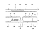
第3保護膜180z上には、画素電極191が形成されている。画素電極191は、データ線171の第1屈曲部および第2屈曲部とほぼ並んだ屈曲縁(curved edge)を含む。画素電極191は複数の第1切開部92を有し、複数の第1切開部92によって定義される複数の第1枝電極192を含む。画素電極191は、図6を参照しながら後述する基準電極199の形態のような第1切開部92およびこれに伴う複数の第1枝電極192を含む。画素電極191の第1切開部92は、ゲート線121が伸びている方向(x方向)と90度をなす縦基準線(y方向に伸びている基準線)と第1角度(θ1)をなす幹部分(main branch portion)、縦基準線と第2角度(θ2)をなす中央部分(center portion)、そして縦基準線と第3角度(θ3)をなすエッジ部分(edge portion)を含む。第2角度(θ2)と第3角度(θ3)は、第1角度(θ1)より大きくてもよい。画素電極191の第1切開部92の幹部分の縦基準線に沿って測定した縦長さは、切開部の全体の縦基準線(y)に沿って測定した縦長さに対して約80%以上の比率を有し、中央部分の縦基準線(y)に沿って測定した縦長さは、切開部の全体の縦長さに対して約6%〜約13%の比率を有し、エッジ部分の縦基準線(y)に沿って測定した縦長さは、切開部の全体の縦長さの約0%〜約10%の比率を有してもよい。明細書全般において、縦長さは、上述したゲート線121が伸びている方向(x方向)と90度をなす縦基準線(y)(y方向に伸びている基準線)に沿って測定した長さを意味する。また、画素電極191の第1切開部92の縦長さに対する中央部分の縦長さの比率と切開部の縦長さに対するエッジ部分の縦長さの比率を合わせた値に10を掛け、液晶表示装置のPPIで割った値が約1以下であってもよい。また、画素電極191の第1切開部92の縦長さに対する中央部分の縦長さの比率と切開部の縦長さに対するエッジ部分の縦長さの比率を合わせた値に一画素の縦長さを掛ければ、約20μm以下であってもよい。また、画素電極191の第1切開部92の縦長さに対する中央部分の縦長さの比率に一画素の縦長さを掛ければ、約5μm以下であってもよい。また、画素電極191の第1切開部92の縦長さに対する各エッジ部分の縦長さの比率に一画素の縦長さを掛ければ、約5μm以下であってもよい。
A
第1保護膜180n、第2保護膜180q、そして第3保護膜180zには、ドレイン電極175を露出する第1接触孔185が形成されている。画素電極191は、第1接触孔185を通じてドレイン電極175と物理的電気的に連結し、ドレイン電極175から電圧の印加を受ける。
A
図に示してはいないが、画素電極191と第3保護膜180z上には配向膜(alignment layer)が塗布されているが、配向膜は水平配向膜であってもよく、一定の方向にラビングされている。しかし、本発明の他の一実施形態に係る液晶表示装置によれば、配向膜は光反応物質を含み、光配向してもよい。
Although not shown in the drawing, an alignment layer is applied on the
以下、上部表示板200について説明する。
Hereinafter, the
透明なガラスまたはプラスチックなどで生成された絶縁基板210上には、遮光部材(light blocking member)220が形成されている。遮光部材220はブラックマトリックス(black matrix)とも呼ばれ、光漏れを防ぐ。
A
基板210上には、さらに複数のカラーフィルタ230が形成されている。下部表示板100の第2保護膜180qがカラーフィルタである場合、上部表示板200のカラーフィルタ230は省略されてもよい。また、上部表示板200の遮光部材220も下部表示板100に形成されてもよい。
A plurality of
カラーフィルタ230および遮光部材220上には、カバー膜(overcoat)250が形成されている。カバー膜250は(有機)絶縁物で生成されてもよく、カラーフィルタ230が露出することを防いで平坦面を提供する。カバー膜250は省略されてもよい。
A
カバー膜250上には、配向膜が配置されていてもよい。
An alignment film may be disposed on the
液晶層3は、正の誘電率異方性を有するネマチック(nematic)液晶物質を含む。液晶層3の液晶分子は、その長軸方向が表示板100、200に平行に配列されており、その方向が下部表示板100の配向膜のラビング方向から上部表示板200に至るまで螺旋状に90度捩じれた構造を有する。
The
画素電極191はドレイン電極175からデータ電圧の印加を受け、基準電極270は表示領域外部に配置されている基準電圧印加部から一定の大きさの基準電圧の印加を受ける。
The
電場生成電極の画素電極191と基準電極270は、電場を生成することにより、2つの電極191、270上に位置する液晶層3の液晶分子は電場の方向と平行な方向に回転する。このように決められた液晶分子の回転方向に応じて液晶層を通過する光の偏光が異なるようになる。
The
以下、図3および図4を参照しながら、本発明の他の一実施形態に係る液晶表示装置について説明する。図3は本発明の他の一実施形態に係る液晶表示装置の配置図であり、図4は図3に示す実施形態に係る液晶表示装置をIV−IV線に沿って切断した断面図である。 Hereinafter, a liquid crystal display device according to another embodiment of the present invention will be described with reference to FIGS. 3 and 4. FIG. 3 is a layout view of a liquid crystal display device according to another embodiment of the present invention, and FIG. 4 is a cross-sectional view taken along the line IV-IV of the liquid crystal display device according to the embodiment shown in FIG. .
図3および図4を参照すれば、本実施形態に係る液晶表示装置は、図1および図2に示す実施形態に係る液晶表示装置とほぼ類似している。 3 and 4, the liquid crystal display device according to the present embodiment is substantially similar to the liquid crystal display device according to the embodiment shown in FIGS. 1 and 2.
図3および図4を参照すれば、本発明の一実施形態に係る液晶表示装置は、互いに対向する下部表示板100および上部表示板200と、その間に注入されている液晶層3を含む。以下では1つの画素領域を例示して説明するが、本発明の実施形態に係る液晶表示装置は約200PPI以上の解像度を有してもよい。すなわち、液晶表示装置のうち、横と縦が約1インチ(inch)の領域内に約200以上の画素が含まれる。また、本発明の実施形態に係る液晶表示装置の1つの画素の横長さ(L1)は約40μm以下であり、縦長さ(L2)は約120μm以下であってもよい。ここで、図に示すように、画素の横長さ(L1)は隣接した2つのデータ線171の縦中央部分の間の間隔であり、画素の縦長さ(L2)は隣接した2つのゲート線121の横中央部分の間の間隔を意味する。
3 and 4, the liquid crystal display according to an exemplary embodiment of the present invention includes a
先ず、下部表示板100について説明する。
First, the
絶縁基板110上には、ゲート線121を含むゲート導電体が形成されている。
A gate conductor including the
ゲート導電体121上には、窒化シリコン(SiNx)または酸化シリコン(SiOx)などからなるゲート絶縁膜140が形成されている。
On the
ゲート絶縁膜140上には、半導体154が形成されている。
A
半導体154上には、抵抗性接触部材163、165が形成されている。半導体154が酸化物半導体である場合、抵抗性接触部材163、165は省略が可能である。
抵抗性接触部材163、165およびゲート絶縁膜140上には、ソース電極173を含むデータ線171とドレイン電極175を含むデータ導電体が形成されている。
A data conductor including a
ドレイン電極175の直ぐ上には、画素電極191が形成されている。画素電極191は面型、すなわち板形態を有し、1つの画素領域に配置される。
A
データ導電体171、173、175、ゲート絶縁膜140、半導体154の露出した部分、そして画素電極191上には、保護膜180が配置される。しかし、本発明の他の実施形態に係る液晶表示装置では、画素電極191とデータ線171の間に保護膜180が配置され、画素電極191は保護膜180に形成された接触孔(図示せず)を通じてドレイン電極175と連結してもよい。
A
保護膜180上には、基準電極270が形成されている。基準電極270は互いに連結し、表示領域外部に配置されている基準電圧印加部から基準電圧の印加を受ける。
A
基準電極270は、データ線171の第1屈曲部および第2屈曲部とほぼ並んだ屈曲縁を含み、隣接画素に配置されている基準電極270は互いに連結している。基準電極270は複数の第2切開部272を有し、複数の第2切開部272によって定義される複数の第2枝電極271を含む。基準電極270は、図6を参照しながら後述する基準電極199の形態のような第2切開部272およびこれに伴う複数の第2枝電極271を含む。基準電極270の第2切開部272は、ゲート線121が伸びている方向(x方向)と90度をなす縦基準線(y方向に伸びている基準線)と第1角度(θ1)をなす幹部分M(main branch portion)、縦基準線と第2角度(θ2)をなす中央部分C(center portion)、そして縦基準線と第3角度(θ3)をなすエッジ部分E(edge portion)を含む。第2角度(θ2)と第3角度(θ3)は、第1角度(θ1)より大きくてもよい。基準電極270の第2切開部272の幹部分の縦長さは切開部の縦長さに約80%以上の比率を有し、中央部分の縦長さは切開部の縦長さの約6%〜約13%の比率を有し、エッジ部分の縦長さは切開部の縦長さの約0%〜約10%の比率を有してもよい。また、基準電極270の第2切開部272の縦長さに対する中央部分の縦長さの比率と切開部の縦長さに対するエッジ部分の縦長さの比率を合わせた値に10を掛け、液晶表示装置のPPIで割った値が約1以下であってもよい。また、基準電極270の第2切開部272の縦長さに対する中央部分の縦長さの比率と切開部の縦長さに対するエッジ部分の縦長さの比率を合わせた値に一画素の縦長さを掛ければ、約20μm以下であってもよい。また、基準電極270の第2切開部272の縦長さに対する中央部分の縦長さの比率に一画素の縦長さを掛ければ、約5μm以下であってもよい。また、基準電極270の第2切開部272の縦長さに対する各エッジ部分の縦長さの比率に一画素の縦長さを掛ければ、約5μm以下であってもよい。
The
図に示してはいないが、基準電極270と保護膜180上には配向膜が塗布されているが、配向膜は水平配向膜であってもよく、一定の方向にラビングされている。しかし、本発明の他の一実施形態に係る液晶表示装置によれば、配向膜は光反応物質を含み、光配向してもよい。
Although not shown in the drawing, an alignment film is applied on the
以下、上部表示板200について説明する。
Hereinafter, the
絶縁基板210上には、遮光部材220が形成されている。基板210上には、複数のカラーフィルタ230も形成されている。カラーフィルタ230は下部表示板100上に配置されてもよいが、この場合、遮光部材220も下部表示板100に配置されてもよい。
A
カラーフィルタ230および遮光部材220上には、カバー膜250が形成されている。カバー膜250は省略されてもよい。
A
カバー膜250上には、配向膜が配置されていてもよい。液晶層3は、正の誘電率異方性を有するネマチック(nematic)液晶物質を含む。液晶層3の液晶分子は、その長軸方向が表示板100、200に平行に配列されているが、その方向が下部表示板100の配向膜のラビング方向から上部表示板200に至るまで螺旋状に90度捩じれた構造を有する。
An alignment film may be disposed on the
以下、図5を参照しながら、本発明の他の一実施形態に係る液晶表示装置について説明する。図5は、本発明の他の一実施形態に係る液晶表示装置の配置図である。 Hereinafter, a liquid crystal display device according to another embodiment of the present invention will be described with reference to FIG. FIG. 5 is a layout view of a liquid crystal display device according to another embodiment of the present invention.
図5を参照すれば、本実施形態に係る液晶表示装置は、図1および図2に示す実施形態に係る液晶表示装置と類似している。類似した構成要素についての具体的な説明は省略する。 Referring to FIG. 5, the liquid crystal display device according to the present embodiment is similar to the liquid crystal display device according to the embodiment shown in FIGS. Detailed description of similar components will be omitted.
しかし、本実施形態に係る液晶表示装置は、図1および図2に示す実施形態に係る液晶表示装置とは異なり、ゲート線121のようにゲート導電体からなる基準電圧線131をさらに含む。基準電圧線131は一定の基準電圧を伝達し、基準電極270との接続のための拡張部を含む。基準電圧線131はゲート線121と平行してもよく、ゲート線121と同一物質で形成されてもよい。
However, unlike the liquid crystal display device according to the embodiment shown in FIGS. 1 and 2, the liquid crystal display device according to the present embodiment further includes a
基準電極270は、第1保護膜180nおよび第2保護膜180qに形成されている第2接触孔138を通じて基準電圧線131と物理的電気的に連結し、基準電圧線131から一定の大きさの共通電圧が伝達されてもよい。
The
基準電極270は互いに連結し、表示領域外部に配置されている基準電圧印加部から基準電圧の印加を受けてもよいが、基準電圧線131と連結して基準電圧の印加を受けることにより、表示領域内で基準電圧降下などを防ぐことができる。
The
図1および図2を参照しながら上述した実施形態に係る液晶表示装置のように、本実施形態に係る液晶表示装置の画素電極191は、図6を参照しながら後述する基準電極199の形態のような第1切開部92およびこれに伴う複数の第1枝電極192を含む。画素電極191の第1切開部92は、ゲート線121が伸びている方向(x方向)と90度をなす縦基準線(y方向に伸びている基準線)と第1角度(θ1)をなす幹部分(main branch portion)、縦基準線と第2角度(θ2)をなす中央部分(center portion)、そして縦基準線と第3角度(θ3)をなすエッジ部分(edge portion)を含む。第2角度(θ2)と第3角度(θ3)は、第1角度(θ1)より大きくてもよい。画素電極191の第1切開部92の幹部分の縦長さは切開部の縦長さに約80%以上の比率を有し、中央部分の縦長さは切開部の縦長さの約6%〜約13%の比率を有し、エッジ部分の縦長さは切開部の縦長さの約0%〜約10%の比率を有してもよい。また、画素電極191の縦長さに対する中央部分の縦長さの比率と切開部の縦長さに対するエッジ部分の縦長さの比率を合わせた値に10を掛け、液晶表示装置のPPIで割った値が約1以下であってもよい。また、画素電極191の第1切開部92の縦長さに対する中央部分の縦長さの比率と切開部の縦長さに対するエッジ部分の縦長さの比率を合わせた値に一画素の縦長さを掛ければ、約20μm以下であってもよい。また、画素電極191の第1切開部92の縦長さに対する中央部分の縦長さの比率に一画素の縦長さを掛ければ、約5μm以下であってもよい。また、画素電極191の第1切開部92の縦長さに対する各エッジ部分の縦長さの比率に一画素の縦長さを掛ければ、約5μm以下であってもよい。
Like the liquid crystal display device according to the embodiment described above with reference to FIGS. 1 and 2, the
以下、図6を参照しながら、本発明の一実施形態に係る液晶表示装置の電場生成電極の基本電極199について説明する。
Hereinafter, the
図6を参照すれば、本発明の一実施形態に係る液晶表示装置の電場生成電極の基本電極の切開部は、ゲート線が伸びている方向(x方向)と90度をなす縦基準線(y方向に伸びている基準線)と第1角度(θ1)をなす幹部分M(main branch portion)(MS)、縦基準線と第2角度(θ2)をなす中央部分C(center portion)(CS)、そして縦基準線と第3角度(θ3)をなすエッジ部分E(edge portion)(ES)を含む。第2角度(θ2)と第3角度(θ3)は、第1角度(θ1)より大きくてもよい。例えば、第1角度(θ1)は約5度〜約20度であってもよく、第2角度(θ2)は約40度〜約50度であってもよい。 Referring to FIG. 6, the incision portion of the basic electrode of the electric field generating electrode of the liquid crystal display device according to the embodiment of the present invention has a vertical reference line (90 degrees) with the direction in which the gate line extends (x direction). A main portion M (main branch portion) (MS) that forms a first angle (θ1) with a reference line extending in the y direction, and a central portion C (center portion) that forms a second angle (θ2) with the vertical reference line CS) and an edge portion E (edge portion) (ES) that forms a third angle (θ3) with the vertical reference line. The second angle (θ2) and the third angle (θ3) may be larger than the first angle (θ1). For example, the first angle (θ1) may be about 5 degrees to about 20 degrees, and the second angle (θ2) may be about 40 degrees to about 50 degrees.
このように、電場生成電極の基本電極の切開部を、幹部分(MS)以外にも、縦基準線となる角度が幹部分(MS)よりも大きい中央部分(CS)とエッジ部分(ES)をさらに含むように形成する。すなわち、幹部分(MS)と中央部分(CS)の境界部で切開部は大きい角度に折れており、幹部分(MS)とエッジ部分(ES)の境界部で切開部は大きい角度に折れている。したがって、中央部分(CS)とエッジ部分(ES)に外部から圧力などが加えられたとき、外部圧力によって不規則になる液晶分子の位置が幹部分(MS)に広がることを防ぐことができる。具体的に、中央部分(CS)とエッジ部分(ES)で発生する液晶分子の不規則な動きは、大きい角度をなして折れている幹部分(MS)との境界部に移動できなくなる。したがって、外部圧力などにより輝度が不均一に現れる現象(bruising)を防ぐことができる。 As described above, in addition to the trunk portion (MS), the incision portion of the basic electrode of the electric field generating electrode has a central portion (CS) and an edge portion (ES) whose vertical reference line is larger than the trunk portion (MS). Is further included. That is, the incision is bent at a large angle at the boundary between the trunk portion (MS) and the central portion (CS), and the incision is bent at a large angle at the boundary between the trunk portion (MS) and the edge portion (ES). Yes. Therefore, when a pressure or the like is applied from the outside to the central portion (CS) and the edge portion (ES), the position of the liquid crystal molecules that become irregular due to the external pressure can be prevented from spreading to the trunk portion (MS). Specifically, the irregular movement of the liquid crystal molecules generated at the central portion (CS) and the edge portion (ES) cannot move to the boundary portion with the trunk portion (MS) that is bent at a large angle. Therefore, it is possible to prevent a phenomenon in which luminance appears unevenly due to external pressure or the like.
上述したように、本発明の実施形態に係る液晶表示装置は、約200PPI以上の解像度を有してもよい。すなわち、液晶表示装置のうち、横と縦が約1インチ(inch)の領域内に約200以上の画素が含まれてもよい。また、本発明の実施形態に係る液晶表示装置の1つの画素の横長さは約40μm以下であり、縦長さは約120μm以下であってもよい。 As described above, the liquid crystal display device according to the embodiment of the present invention may have a resolution of about 200 PPI or more. That is, in the liquid crystal display device, about 200 or more pixels may be included in a region of about 1 inch in width and length. In addition, the horizontal length of one pixel of the liquid crystal display device according to the embodiment of the present invention may be about 40 μm or less, and the vertical length may be about 120 μm or less.
電場生成電極の基本電極の切開部の幹部分(MS)の縦長さは切開部の全体縦長さに約80%以上の比率を有し、中央部分(CS)の縦長さは切開部の全体縦長さの約6%〜約13%の比率を有し、エッジ部分(ES)の縦長さは切開部の全体縦長さの約0%〜約10%の比率を有してもよい。 The vertical length of the trunk portion (MS) of the incision portion of the basic electrode of the electric field generating electrode has a ratio of about 80% or more to the overall vertical length of the incision portion, and the vertical length of the central portion (CS) is the overall vertical length of the incision portion. The length of the edge portion (ES) may have a ratio of about 0% to about 10% of the overall length of the incision.
切開部の中央部分(CS)が占める縦長さと切開部のエッジ部分(ES)が占める縦長さは約5μm以下であってもよく、切開部全体が占める領域の縦長さは約100μmであってもよい。 The vertical length occupied by the central portion (CS) of the incision portion and the vertical length occupied by the edge portion (ES) of the incision portion may be about 5 μm or less, and the vertical length of the region occupied by the entire incision portion may be about 100 μm. Good.
また、切開部の全体縦長さに対する中央部分(CS)の縦長さの比率(%)と切開部の全体縦長さに対するエッジ部分(ES)の縦長さの比率(%)を合わせた値に10を掛け、液晶表示装置のPPIで割った値が約1以下であってもよい。 Further, 10 is set to a value obtained by combining the ratio (%) of the vertical length of the central portion (CS) to the total vertical length of the incised portion and the ratio (%) of the vertical length of the edge portion (ES) to the total vertical length of the incised portion. The value divided by the PPI of the liquid crystal display device may be about 1 or less.
また、切開部の全体縦長さに対する中央部分(CS)の縦長さの比率と切開部の全体縦長さに対するエッジ部分(ES)の縦長さの比率を合わせた値に一画素の縦長さを掛ければ、約20μm以下であってもよい。 Also, if the ratio of the vertical length of the central portion (CS) to the overall vertical length of the incision portion and the ratio of the vertical length of the edge portion (ES) to the overall vertical length of the incision portion is multiplied by the vertical length of one pixel About 20 μm or less.
また、切開部の全体縦長さに対する中央部分(CS)の縦長さの比率に一画素の縦長さを掛ければ、約5μm以下であってもよい。 Further, if the ratio of the vertical length of the central portion (CS) to the overall vertical length of the incised portion is multiplied by the vertical length of one pixel, it may be about 5 μm or less.
また、切開部の全体縦長さに対するエッジ部分(ES)の縦長さの比率に一画素の縦長さを掛ければ、約5μm以下であってもよい。 Further, if the ratio of the vertical length of the edge portion (ES) to the overall vertical length of the incised portion is multiplied by the vertical length of one pixel, it may be about 5 μm or less.
このように、電場生成電極の切開部の幹部分(MS)の全体切開部長さに対する比率を高め、中央部分(CS)およびエッジ部分(ES)の比率を減らすことにより、液晶表示装置の透過率を高めることができる。 Thus, by increasing the ratio of the trunk portion (MS) of the incision portion of the electric field generating electrode to the overall incision length and reducing the ratio of the central portion (CS) and the edge portion (ES), the transmittance of the liquid crystal display device Can be increased.
以下、表1と表2、そして図7を参照しながら、本発明の一実験例に係る液晶表示装置の透過率について説明する。 Hereinafter, the transmittance of the liquid crystal display device according to an experimental example of the present invention will be described with reference to Tables 1 and 2 and FIG.
本実験例では、液晶表示装置の解像度、例えばPPI、すなわち液晶表示装置のうち、横と縦が約1インチ(inch)の領域内に配置される画素の総数、画素の横長さと縦長さ、切開部の長さ、切開部の中央部分(CS)の長さ、切開部のエッジ部分(ES)の長さなどを変化させながら透過率を測定し、その結果を表1に示した。例えば、既存の液晶表示装置でのように、切開部の全体縦長さに対する切開部の中央部分(CS)の縦長さの比率とエッジ部分(ES)の縦長さの比率を形成した場合(Case A1、Case A2、Case A3)と本発明の実施形態に係る液晶表示装置のように、切開部の全体縦長さに対する切開部の中央部分(CS)の縦長さの比率とエッジ部分(ES)の縦長さの比率を調節した場合(Case B1、Case B2、Case B3、Case B4、Case B5)とに分けて透過率を測定した。その他の条件はすべて同じであった。本実験例で製作したすべての液晶表示装置で同じ圧力を加えたとき、外部圧力などにより輝度が不均一に現れる現象(bruising) は発生しなかった。 In this experimental example, the resolution of the liquid crystal display device, for example, PPI, that is, the total number of pixels arranged in an area of about 1 inch in the horizontal and vertical directions in the liquid crystal display device, the horizontal and vertical lengths of the pixels, the incision The transmittance was measured while changing the length of the cut portion, the length of the central portion (CS) of the incised portion, the length of the edge portion (ES) of the cut portion, and the results are shown in Table 1. For example, when the ratio of the vertical length of the central portion (CS) of the incised portion and the vertical length of the edge portion (ES) to the entire vertical length of the incised portion is formed as in an existing liquid crystal display device (Case A1) , Case A2, Case A3) and the ratio of the vertical length of the central portion (CS) of the incised portion to the overall vertical length of the incised portion and the vertical length of the edge portion (ES) as in the liquid crystal display device according to the embodiment of the present invention. The transmittance was measured separately when the ratio was adjusted (Case B1, Case B2, Case B3, Case B4, Case B5). All other conditions were the same. When the same pressure was applied to all the liquid crystal display devices manufactured in this experimental example, a phenomenon in which luminance appeared uneven due to external pressure or the like did not occur.

表1を参照すれば、切開部の全体長さに対する切開部の中央部分(CS)の比率とエッジ部分(ES)の比率を相対的に大きく、例えば、切開部のエッジ部分(ES)の比率を約7.5μで形成し、エッジ部分(ES)の比率を約15%以上で形成した場合(Case A1、Case A2、Case A3)に比べ、本発明の実施形態に係る液晶表示装置のように、切開部の全体長さに対する切開部の中央部分(CS)の比率とエッジ部分(ES)の比率を調節した場合(Case B1、Case B2、Case B3、Case B4、Case B5)、液晶表示装置のPPIを大きく形成しても、液晶表示装置の透過率が増加したことが分かった。すなわち、本発明の実施形態に係る液晶表示装置のように、切開部の全体長さに対する切開部の中央部分(CS)の比率とエッジ部分(ES)の比率を調節すれば、液晶表示装置を高解像度に形成しても、液晶表示装置の透過率が増加することが分かった。
Referring to Table 1, the ratio of the central part (CS) of the incision part and the ratio of the edge part (ES) to the entire length of the incision part is relatively large, for example, the ratio of the edge part (ES) of the incision part Compared to the case where the edge portion (ES) is formed at a ratio of about 15% or more (Case A1, Case A2, Case A3), as in the liquid crystal display device according to the embodiment of the present invention. In addition, when the ratio of the central part (CS) of the incision part and the ratio of the edge part (ES) to the entire length of the incision part is adjusted (Case B1, Case B2, Case B3, Case B4, Case B5), liquid crystal display It was found that the transmittance of the liquid crystal display device increased even when the PPI of the device was made large. That is, as in the liquid crystal display device according to the embodiment of the present invention, by adjusting the ratio of the central portion (CS) of the incision portion and the ratio of the edge portion (ES) to the entire length of the incision portion, the liquid crystal display device can be obtained. It has been found that the transmittance of the liquid crystal display device is increased even when it is formed at a high resolution.
このように、本発明の実施形態に係る液晶表示装置では、外部圧力などにより輝度が不均一に現れる現象(bruising)を防ぎながらも、液晶表示装置の透過率減少を防ぐことができることが分かった。 As described above, the liquid crystal display device according to the embodiment of the present invention can prevent a decrease in transmittance of the liquid crystal display device while preventing a phenomenon in which luminance is unevenly generated due to an external pressure or the like. .
また、本発明の実施形態に係る液晶表示装置のように、切開部の全体長さに対する中央部分(CS)の比率と切開部の全体長さに対するエッジ部分(ES)の比率を合わせた値に一画素の縦長さを掛けた値Bが約20μm以下である場合(Case B1、Case B2、Case B3、Case B4、Case B5)、透過率が増加したことが分かった。 Further, like the liquid crystal display device according to the embodiment of the present invention, the ratio of the central portion (CS) to the entire length of the incised portion and the ratio of the edge portion (ES) to the entire length of the incised portion are combined. When the value B multiplied by the vertical length of one pixel is about 20 μm or less (Case B1, Case B2, Case B3, Case B4, Case B5), it was found that the transmittance increased.
また、本発明の実施形態に係る液晶表示装置のように、切開部の全体長さに対する中央部分(CS)の比率に一画素の縦長さをかけた値Cが約5μm以下である場合(Case B1、Case B2、Case B3、Case B4、Case B5)、透過率が増加したことが分かった。 Further, as in the liquid crystal display device according to the embodiment of the present invention, a value C obtained by multiplying the ratio of the central portion (CS) to the entire length of the incised portion by the vertical length of one pixel is about 5 μm or less (Case B1, Case B2, Case B3, Case B4, Case B5), it was found that the transmittance increased.
また、本発明の実施形態に係る液晶表示装置のように、切開部の全体長さに対する各エッジ部分(ES)の比率に一画素の縦長さを掛けた値Dが約5μm以下である場合(Case B1、Case B2、Case B3、Case B4、Case B5)、透過率が増加したことが分かった。 Further, as in the liquid crystal display device according to the embodiment of the present invention, when a value D obtained by multiplying the ratio of each edge portion (ES) to the entire length of the incised portion by the vertical length of one pixel is about 5 μm or less ( Case B1, Case B2, Case B3, Case B4, Case B5), it was found that the transmittance increased.
以下、図7を参照しながら、本発明の一実験例に係る液晶表示装置の外部圧力などにより輝度が不均一に現れる現象(bruising)について説明する。図7は、本発明の一実験例に係る液晶表示装置の一部の透過率結果を示す電子顕微鏡写真である。 Hereinafter, a phenomenon in which luminance appears uneven due to an external pressure of a liquid crystal display device according to an experimental example of the present invention will be described with reference to FIG. FIG. 7 is an electron micrograph showing the transmittance results of a part of the liquid crystal display device according to an experimental example of the present invention.
本実験例では、表1を参照して上述した実験例において、2つの場合(Case A1とCase B4)で第2角度(θ2)を変化させた。具体的に、既存の液晶表示装置のように、電場生成電極の切開部の中央部分(CS)の縦長さを約10μmに形成して第2角度(θ2)を約25度に形成した場合(Case A1)と、本発明の実施形態に係る液晶表示装置のように、電場生成電極の切開部の中央部分(CS)の縦長さを約5μmに形成して第2角度(θ2)を約45度に形成した場合(Case B4)に対して同じ大きさの外部圧力を加えた後、切開部の中央部分を電子顕微鏡で観察し、その結果を図7に示した。 In this experimental example, in the experimental example described above with reference to Table 1, the second angle (θ2) was changed in two cases (Case A1 and Case B4). Specifically, as in an existing liquid crystal display device, when the vertical length of the central portion (CS) of the incision portion of the electric field generating electrode is formed to about 10 μm and the second angle (θ2) is formed to about 25 degrees ( As in the case A1) and the liquid crystal display device according to the embodiment of the present invention, the vertical length of the central portion (CS) of the incision portion of the electric field generating electrode is formed to be about 5 μm, and the second angle (θ2) is about 45 μm. After applying the same external pressure to the case (Case B4), the central part of the incision was observed with an electron microscope, and the result is shown in FIG.
図7において、(a)は本実験例の場合(Case A1)の結果を示し、(b)は本実験例の場合(Case B4)の結果を示している。 In FIG. 7, (a) shows the result of the present experimental example (Case A1), and (b) shows the result of the present experimental example (Case B4).
図7を参照すれば、同じ外部圧力が加えられた場合、本発明の実施形態のような場合(Case B4)でも、既存の液晶表示装置の場合(Case A1)のように、液晶の不規則な動きによる透過率低下部分は切開部の中央部分(CS)にのみ発生し、切開部の幹部分(MS)にまで拡散していないことが分かった。このように、本発明の実施形態に係る液晶表示装置は、外部圧力による液晶分子の不規則な動きが切開部に沿って移動することを防ぐと同時に、高解像度の液晶表示装置において透過率低下を防げることが分かった。 Referring to FIG. 7, when the same external pressure is applied, even in the case of the embodiment of the present invention (Case B4), as in the case of the existing liquid crystal display device (Case A1), the irregularity of the liquid crystal It was found that the transmittance-decreasing part due to a simple movement occurred only in the central part (CS) of the incision and did not diffuse to the trunk part (MS) of the incision. As described above, the liquid crystal display device according to the embodiment of the present invention prevents the irregular movement of the liquid crystal molecules due to the external pressure from moving along the incision, and at the same time, reduces the transmittance in the high-resolution liquid crystal display device. I found out that
以下、図8〜図14を参照しながら、本発明の他の実施形態に係る液晶表示装置の電場生成電極の基本電極の切開部について説明する。図8〜図14は、本発明の他の実施形態に係る液晶表示装置の電場生成電極の切開部を示す配置図である。 Hereinafter, an incision portion of a basic electrode of an electric field generating electrode of a liquid crystal display device according to another embodiment of the present invention will be described with reference to FIGS. 8 to 14 are arrangement views illustrating cut portions of the electric field generating electrode of the liquid crystal display device according to another embodiment of the present invention.
図8を参照すれば、本実施形態に係る液晶表示装置の電場生成電極の基本電極の切開部は、図1〜図6を参照しながら説明した実施形態に係る液晶表示装置の電場生成電極の基本電極の切開部と類似している。 Referring to FIG. 8, the incision of the basic electrode of the electric field generating electrode of the liquid crystal display device according to the present embodiment is the same as that of the electric field generating electrode of the liquid crystal display device according to the embodiment described with reference to FIGS. Similar to the basic electrode incision.
電場生成電極の基本電極の切開部は、ゲート線が伸びている方向と90度をなす縦基準線と第1角度(θ1)をなす幹部分(MS)、縦基準線と第2角度(θ2)をなす中央部分(CS)、そして縦基準線と第3角度(θ3)をなすエッジ部分(ES)を含む。第2角度(θ2)と第3角度(θ3)は、第1角度(θ1)より大きくてもよい。 The cut-out portion of the basic electrode of the electric field generating electrode includes a trunk portion (MS) that forms a first angle (θ1) with a vertical reference line that forms 90 degrees with the direction in which the gate line extends, and a vertical reference line and a second angle (θ2). ) Forming a central portion (CS) and an edge portion (ES) forming a third angle (θ3) with the vertical reference line. The second angle (θ2) and the third angle (θ3) may be larger than the first angle (θ1).
しかし、本実施形態に係る液晶表示装置の電場生成電極の基本電極の切開部のエッジ部分(ES)は、画素領域の下部に配置されている第1エッジ部分(ES1)と画素領域の上部に配置されている第2エッジ部分(ES2)を有する。 However, the edge portion (ES) of the cut-out portion of the basic electrode of the electric field generating electrode of the liquid crystal display device according to the present embodiment is located above the first edge portion (ES1) disposed below the pixel region and the pixel region. It has the 2nd edge part (ES2) arranged.
第2エッジ部分(ES2)が縦基準線となす角度(θ3b)は第1エッジ部分(ES1)が縦基準線となす角度(θ3a)よりも小さく、第2エッジ部分(ES2)の長さは第1エッジ部分(ES1)の長さよりも短い。 The angle (θ3b) that the second edge portion (ES2) makes with the vertical reference line is smaller than the angle (θ3a) that the first edge portion (ES1) makes with the vertical reference line, and the length of the second edge portion (ES2) is It is shorter than the length of the first edge portion (ES1).
また、第2エッジ部分(ES2)の端部は、電場生成電極で囲まれておらずに開いている。 Further, the end portion of the second edge portion (ES2) is open without being surrounded by the electric field generating electrode.
図1〜図6を参照しながら上述した実施形態に係る液晶表示装置のすべての特徴は、本実施形態に係る液晶表示装置にすべて適用が可能である。 All the features of the liquid crystal display device according to the embodiment described above with reference to FIGS. 1 to 6 can be applied to the liquid crystal display device according to this embodiment.
図9および図10を参照すれば、本実施形態に係る液晶表示装置の電場生成電極の基本電極の切開部は、図1〜図6を参照しながら上述した実施形態に係る液晶表示装置の電場生成電極の基本電極の切開部、そして図8を参照しながら説明した実施形態に係る液晶表示装置の電場生成電極の基本電極の切開部と類似している。 Referring to FIGS. 9 and 10, the cut-out portion of the basic electrode of the electric field generating electrode of the liquid crystal display device according to the present embodiment is the electric field of the liquid crystal display device according to the embodiment described above with reference to FIGS. The cutout portion of the basic electrode of the generation electrode and the cutout portion of the basic electrode of the electric field generation electrode of the liquid crystal display device according to the embodiment described with reference to FIG.
図9および図10を参照すれば、電場生成電極の基本電極の切開部は、ゲート線が伸びている方向と90度をなす縦基準線と第1角度(θ1)をなす幹部分(MS)、縦基準線と第2角度(θ2)をなす中央部分(CS)、そして縦基準線と第3角度(θ3)をなすエッジ部分(ES)を含む。第2角度(θ2)と第3角度(θ3)は、第1角度(θ1)より大きくてもよい。 Referring to FIGS. 9 and 10, the incision of the basic electrode of the electric field generating electrode is a trunk portion (MS) that forms a first angle (θ1) with the vertical reference line that forms 90 degrees with the direction in which the gate line extends. , A central part (CS) forming a second angle (θ2) with the vertical reference line, and an edge part (ES) forming a third angle (θ3) with the vertical reference line. The second angle (θ2) and the third angle (θ3) may be larger than the first angle (θ1).
しかし、本実施形態に係る液晶表示装置の電場生成電極の基本電極の切開部のエッジ部分(ES)は、画素領域の下部に配置されている第1エッジ部分(ES1)と画素領域の上部に配置されている第2エッジ部分(ES2)を有する。 However, the edge portion (ES) of the cut-out portion of the basic electrode of the electric field generating electrode of the liquid crystal display device according to the present embodiment is located above the first edge portion (ES1) disposed below the pixel region and the pixel region. It has the 2nd edge part (ES2) arranged.
第2エッジ部分(ES2)が縦基準線となす角度(θ3b)は第1エッジ部分(ES1)が縦基準線となす角度(θ3a)よりも小さく、第2エッジ部分(ES2)の長さは第1エッジ部分(ES1)の長さよりも短い。 The angle (θ3b) that the second edge portion (ES2) makes with the vertical reference line is smaller than the angle (θ3a) that the first edge portion (ES1) makes with the vertical reference line, and the length of the second edge portion (ES2) is It is shorter than the length of the first edge portion (ES1).
また、第2エッジ部分(ES2)の端部は、電場生成電極で囲まれておらずに開いている。 Further, the end portion of the second edge portion (ES2) is open without being surrounded by the electric field generating electrode.
図8に示す実施形態に係る液晶表示装置の電場生成電極の基本電極の切開部の第2エッジ部分(ES2)の端部が隣接した基本電極の幹部となす間隔(d1)に比べ、図9および図10に示す実施形態に係る液晶表示装置の電場生成電極の基本電極の切開部の第2エッジ部分(ES2)の端部が隣接した基本電極の幹部となす間隔(d2)および(d3)は互いに異なる。例えば、d1>d2>d3の関係を有している。 Compared to the interval (d1) between the end of the second edge portion (ES2) of the cut-out portion of the basic electrode of the electric field generating electrode of the liquid crystal display device according to the embodiment shown in FIG. And the interval (d2) and (d3) between the end of the second edge portion (ES2) of the cut-out portion of the basic electrode of the electric field generating electrode of the liquid crystal display device according to the embodiment shown in FIG. 10 and the trunk of the adjacent basic electrode Are different from each other. For example, it has a relationship of d1> d2> d3.
図1〜図6を参照しながら上述した実施形態に係る液晶表示装置のすべての特徴は、本実施形態に係る液晶表示装置にすべて適用が可能である。 All the features of the liquid crystal display device according to the embodiment described above with reference to FIGS. 1 to 6 can be applied to the liquid crystal display device according to this embodiment.
図11を参照すれば、本実施形態に係る液晶表示装置の電場生成電極の基本電極の切開部は、図1〜図6を参照しながら説明した実施形態に係る液晶表示装置の電場生成電極の基本電極の切開部と類似している。 Referring to FIG. 11, the incision portion of the basic electrode of the electric field generating electrode of the liquid crystal display device according to the present embodiment is the same as that of the electric field generating electrode of the liquid crystal display device according to the embodiment described with reference to FIGS. 1 to 6. Similar to the basic electrode incision.
電場生成電極の基本電極の切開部は、ゲート線が伸びている方向と90度をなす縦基準線と第1角度(θ1)をなす幹部分(MS)、縦基準線と第2角度(θ2)をなす中央部分(CS)、そして縦基準線と第3角度(θ3)をなすエッジ部分(ES)を含む。第2角度(θ2)と第3角度(θ3)は、第1角度(θ1)より大きくてもよい。 The cut-out portion of the basic electrode of the electric field generating electrode includes a trunk portion (MS) that forms a first angle (θ1) with a vertical reference line that forms 90 degrees with the direction in which the gate line extends, and a vertical reference line and a second angle (θ2). ) Forming a central portion (CS) and an edge portion (ES) forming a third angle (θ3) with the vertical reference line. The second angle (θ2) and the third angle (θ3) may be larger than the first angle (θ1).
しかし、本実施形態に係る液晶表示装置の電場生成電極の基本電極の切開部のエッジ部分(ES)は、画素領域の下部に配置されている第1エッジ部分(ES1)と画素領域の上部に配置されている第2エッジ部分(ES2)を有する。 However, the edge portion (ES) of the cut-out portion of the basic electrode of the electric field generating electrode of the liquid crystal display device according to the present embodiment is located above the first edge portion (ES1) disposed below the pixel region and the pixel region. It has the 2nd edge part (ES2) arranged.
第2エッジ部分(ES2)が縦基準線となす角度(θ3b)は第1エッジ部分(ES1)が縦基準線となす角度(θ3a)よりも小さく、第2エッジ部分(ES2)の長さは第1エッジ部分(ES1)の長さよりも短い。 The angle (θ3b) that the second edge portion (ES2) makes with the vertical reference line is smaller than the angle (θ3a) that the first edge portion (ES1) makes with the vertical reference line, and the length of the second edge portion (ES2) is It is shorter than the length of the first edge portion (ES1).
また、図8〜図10に示す実施形態に係る液晶表示装置とは異なり、第2エッジ部分(ES2)の端部は電場生成電極で囲まれている。 Further, unlike the liquid crystal display device according to the embodiment shown in FIGS. 8 to 10, the end portion of the second edge portion (ES2) is surrounded by the electric field generating electrode.
図1〜図6を参照しながら上述した実施形態に係る液晶表示装置のすべての特徴は、本実施形態に係る液晶表示装置にすべてに適用が可能である。 All the features of the liquid crystal display device according to the embodiment described above with reference to FIGS. 1 to 6 can be applied to the liquid crystal display device according to this embodiment.
図12を参照すれば、本実施形態に係る液晶表示装置の電場生成電極の基本電極の切開部は、図1〜図6を参照しながら説明した実施形態に係る液晶表示装置の電場生成電極の基本電極の切開部と類似している。 Referring to FIG. 12, the incision of the basic electrode of the electric field generating electrode of the liquid crystal display device according to the present embodiment is the same as that of the electric field generating electrode of the liquid crystal display device according to the embodiment described with reference to FIGS. Similar to the basic electrode incision.
電場生成電極の基本電極の切開部は、ゲート線が伸びている方向と90度をなす縦基準線と第1角度(θ1)をなす幹部分(MS)、縦基準線と第2角度(θ2)をなす中央部分(CS)、そして縦基準線と第3角度(θ3)をなすエッジ部分(ES)を含む。第2角度(θ2)と第3角度(θ3)は、第1角度(θ1)より大きくてもよい。 The cut-out portion of the basic electrode of the electric field generating electrode includes a trunk portion (MS) that forms a first angle (θ1) with a vertical reference line that forms 90 degrees with the direction in which the gate line extends, and a vertical reference line and a second angle (θ2). ) Forming a central portion (CS) and an edge portion (ES) forming a third angle (θ3) with the vertical reference line. The second angle (θ2) and the third angle (θ3) may be larger than the first angle (θ1).
しかし、本実施形態に係る液晶表示装置の電場生成電極の基本電極の切開部のエッジ部分(ES)は、画素領域の下部に配置されている第1エッジ部分(ES1)と画素領域の上部に配置されている第2エッジ部分(ES2)を有する。 However, the edge portion (ES) of the cut-out portion of the basic electrode of the electric field generating electrode of the liquid crystal display device according to the present embodiment is located above the first edge portion (ES1) disposed below the pixel region and the pixel region. It has the 2nd edge part (ES2) arranged.
第2エッジ部分(ES2)が縦基準線となす角度(θ3b)は第1エッジ部分(ES1)が縦基準線となす角度(θ3a)よりも大きく、第2エッジ部分(ES2)の長さは第1エッジ部分(ES1)の長さよりも短い。 The angle (θ3b) that the second edge portion (ES2) makes with the vertical reference line is larger than the angle (θ3a) that the first edge portion (ES1) makes with the vertical reference line, and the length of the second edge portion (ES2) is It is shorter than the length of the first edge portion (ES1).
また、第2エッジ部分(ES2)の端部は、電場生成電極で囲まれておらずに開いている。 Further, the end portion of the second edge portion (ES2) is open without being surrounded by the electric field generating electrode.
図1〜図6を参照しながら上述した実施形態に係る液晶表示装置のすべての特徴は、本実施形態に係る液晶表示装置にすべて適用が可能である。 All the features of the liquid crystal display device according to the embodiment described above with reference to FIGS. 1 to 6 can be applied to the liquid crystal display device according to this embodiment.
図13および図14を参照すれば、本実施形態に係る液晶表示装置の電場生成電極の基本電極の切開部は、図1〜図6を参照しながら説明した実施形態に係る液晶表示装置の電場生成電極の基本電極の切開部、そして図12を参照しながら説明した実施形態に係る液晶表示装置の電場生成電極の基本電極の切開部と類似している。 Referring to FIGS. 13 and 14, the incision portion of the basic electrode of the electric field generating electrode of the liquid crystal display device according to the present embodiment is the electric field of the liquid crystal display device according to the embodiment described with reference to FIGS. 1 to 6. The cutout portion of the basic electrode of the generation electrode is similar to the cutout portion of the basic electrode of the electric field generation electrode of the liquid crystal display device according to the embodiment described with reference to FIG.
図13および図14を参照すれば、電場生成電極の基本電極の切開部は、ゲート線が伸びている方向と90度をなす縦基準線と第1角度(θ1)をなす幹部分(MS)、縦基準線と第2角度(θ2)をなす中央部分(CS)、そして縦基準線と第3角度(θ3)をなすエッジ部分(ES)を含む。第2角度(θ2)と第3角度(θ3)は、第1角度(θ1)より大きくてもよい。 Referring to FIGS. 13 and 14, the incision portion of the basic electrode of the electric field generating electrode is a trunk portion (MS) that forms a first angle (θ1) with the vertical reference line that forms 90 degrees with the direction in which the gate line extends. , A central part (CS) forming a second angle (θ2) with the vertical reference line, and an edge part (ES) forming a third angle (θ3) with the vertical reference line. The second angle (θ2) and the third angle (θ3) may be larger than the first angle (θ1).
しかし、本実施形態に係る液晶表示装置の電場生成電極の基本電極の切開部のエッジ部分(ES)は、画素領域の下部に配置されている第1エッジ部分(ES1)と画素領域の上部に配置されている第2エッジ部分(ES2)を有する。 However, the edge portion (ES) of the cut-out portion of the basic electrode of the electric field generating electrode of the liquid crystal display device according to the present embodiment is located above the first edge portion (ES1) disposed below the pixel region and the pixel region. It has the 2nd edge part (ES2) arranged.
第2エッジ部分(ES2)が縦基準線となす角度(θ3b)は第1エッジ部分(ES1)が縦基準線となす角度(θ3a)よりも大きく、第2エッジ部分(ES2)の長さは第1エッジ部分(ES1)の長さよりも短い。 The angle (θ3b) that the second edge portion (ES2) makes with the vertical reference line is larger than the angle (θ3a) that the first edge portion (ES1) makes with the vertical reference line, and the length of the second edge portion (ES2) is It is shorter than the length of the first edge portion (ES1).
また、第2エッジ部分(ES2)の端部は、電場生成電極で囲まれておらずに開いている。 Further, the end portion of the second edge portion (ES2) is open without being surrounded by the electric field generating electrode.
また、図12に示す実施形態に係る液晶表示装置の電場生成電極の基本電極の切開部の第2エッジ部分(ES2)の端部が隣接した基本電極の幹部となす間隔(d4)に比べ、図13および図14に示す実施形態に係る液晶表示装置の電場生成電極の基本電極の切開部の第2エッジ部分(ES2)の端部が隣接した基本電極の幹部となす間隔(d5)および(d6)は互いに異なる。例えば、d4>d5>d6の関係を有している。 In addition, compared to the interval (d4) between the end of the second edge portion (ES2) of the incision portion of the basic electrode of the electric field generating electrode of the liquid crystal display device according to the embodiment shown in FIG. 12 and the trunk portion of the adjacent basic electrode, The distance (d5) between the end of the second edge portion (ES2) of the cut portion of the basic electrode of the electric field generating electrode of the liquid crystal display device according to the embodiment shown in FIG. 13 and FIG. d6) are different from each other. For example, there is a relationship of d4> d5> d6.
図1〜図6を参照しながら上述した実施形態に係る液晶表示装置のすべての特徴は、本実施形態に係る液晶表示装置にすべて適用が可能である。 All the features of the liquid crystal display device according to the embodiment described above with reference to FIGS. 1 to 6 can be applied to the liquid crystal display device according to this embodiment.
上記構成によれば、高解像度液晶表示装置において2つの電場生成電極を1つの基板上に形成し、2つの電場生成電極のうちの少なくとも1つは切開部を有するように形成し、外部圧力による液晶分子の不規則な動きが切開部に沿って移動することを防ぐと同時に、液晶表示装置の透過率低下を防ぐことができる液晶表示装置を提供することができる。 According to the above configuration, in the high-resolution liquid crystal display device, two electric field generating electrodes are formed on one substrate, and at least one of the two electric field generating electrodes is formed to have an incision, which is caused by external pressure. It is possible to provide a liquid crystal display device capable of preventing irregular movement of liquid crystal molecules from moving along the incision portion and at the same time preventing a decrease in transmittance of the liquid crystal display device.
以上、本発明の好ましい実施形態について詳細に説明したが、本発明の権利範囲はこれに限定されることはなく、添付した特許請求の範囲で定義している本発明の基本概念を利用した当業者の多様な変形および改良形態も本発明の権利範囲に属する。 The preferred embodiment of the present invention has been described in detail above, but the scope of the present invention is not limited to this, and the basic concept of the present invention defined in the appended claims is used. Various modifications and improvements of the merchants are also within the scope of the present invention.
3:液晶層
110、210:絶縁基板
121:ゲート線
124:ゲート電極
131:基準電圧線
140:ゲート絶縁膜
154:半導体
163、165:抵抗性接触部材
171:データ線
173:ソース電極
175:ドレイン電極
180、180n、180q、180z:保護膜
191:画素電極
199:基本電極
270:基準電極
MS:切開部の幹部分
CS:切開部の中央部分
ES:切開部のエッジ部分
3: Liquid crystal layer 110, 210: Insulating substrate 121: Gate line 124: Gate electrode 131: Reference voltage line 140: Gate insulating film 154:
Claims (6)
前記第1基板上に、互いに平行に配置されているゲート線、
前記ゲート線と交差するデータ線、
前記第1基板上に配置されており、絶縁膜を間に挟んで重なる第1電場生成電極と第2電場生成電極を含む複数の画素、及び、
前記第1基板と、前記第1基板に対向する第2基板との間に保持されて、前記第1電場生成電極と第2電場生成電極とにより画素ごとに駆動される液晶層を含み、
各画素は、2つのゲート線の間の中間の箇所にて折れ曲がった、くの字をなし、
各画素中、前記第1電場生成電極と前記第2電場生成電極のうちのいずれか1つは複数の切開部及びこれらにより互いに分けられる複数の枝電極を有し、
各画素における長さ方向の一方の端部に、薄膜トランジスタ(TFT)が備えられ、各画素中、切開部及び枝電極は、前記薄膜トランジスタの近傍から、画素の長さ方向の他端部の近傍にまで延びており、
前記複数の切開部及び前記複数の枝電極は、いずれも、画素がなすくの字に対応して、全体として、波線括弧({)状をなし、前記ゲート線と90度をなす基準線に対して第1角度をなす第1部分、及び、前記基準線に対して前記第1角度とは異なる第2角度をなす第2部分を含み、前記複数の切開部は、いずれも、前記基準線に対して前記第1角度とは異なる第3角度をなす第3部分をさらに含み、
前記各切開部及び前記各枝電極における長さ方向中央部分は、2つの前記第2部分がL字状に組み合わさって形成されており、この両側からそれぞれ、2つの前記第1部分が延びており、
各画素中、前記複数の切開部及び前記各枝電極についての、前記L字状がなす頂点及び前記データ線が折れ曲がる箇所は、ゲート線に平行の、一つの直線上にあり、
前記第1角度は5度〜20度であって、前記第2角度は40度〜50度であり、
前記切開部の縦長さに対する前記第1部分の縦長さの比率は80%以上であり、ここで、前記縦長さは、前記基準線の方向に測定した長さであり、
各画素の縦長さは96〜120μmであり、また、各画素の横長さは32〜40μmであり、ここで、横長さは、前記ゲート線の方向に測定した長さであり、
前記複数の画素の密度は200PPI〜264PPIであり、
前記切開部の縦長さに対する前記第2部分の縦長さの比率は6.3%〜9.9%であり、
前記切開部の縦長さに対する前記第3部分の縦長さの比率は10.1%〜12.6%であり、
各画素の縦長さに対する第3部分の縦長さの比率は、8.3%〜10.4%である、液晶表示装置。 A first substrate,
Gate lines arranged in parallel with each other on the first substrate;
A data line intersecting the gate line;
A plurality of pixels disposed on the first substrate and including a first electric field generating electrode and a second electric field generating electrode that overlap with each other with an insulating film interposed therebetween; and
A liquid crystal layer that is held between the first substrate and a second substrate facing the first substrate and is driven for each pixel by the first electric field generating electrode and the second electric field generating electrode;
Each pixel is folded in the middle between the two gate lines, and has a square shape,
In each pixel, any one of the first electric field generating electrode and the second electric field generating electrode has a plurality of incisions and a plurality of branch electrodes separated from each other.
A thin film transistor (TFT) is provided at one end portion in the length direction of each pixel, and in each pixel, the cut-out portion and the branch electrode are located near the other end portion in the length direction of the pixel from the vicinity of the thin film transistor. Extends to
Each of the plurality of cutout portions and the plurality of branch electrodes has a wavy parenthesis ({) shape as a whole corresponding to the shape of the pixel, and serves as a reference line that forms 90 degrees with the gate line. A first portion that forms a first angle with respect to the reference line; and a second portion that forms a second angle different from the first angle with respect to the reference line. Further comprising a third portion having a third angle different from the first angle,
The central part in the longitudinal direction of each incision and each branch electrode is formed by combining the two second parts in an L shape, and the two first parts extend from both sides. And
In each pixel, the apex formed by the L shape and the portion where the data line is bent on the plurality of cutout portions and the branch electrodes are on a single straight line parallel to the gate line,
The first angle is 5 degrees to 20 degrees, and the second angle is 40 degrees to 50 degrees;
The ratio of the vertical length of the first portion to the vertical length of the incision is 80% or more, wherein the vertical length is a length measured in the direction of the reference line,
The vertical length of each pixel is 96 to 120 μm, and the horizontal length of each pixel is 32 to 40 μm, where the horizontal length is a length measured in the direction of the gate line,
The density of the plurality of pixels is 200 PPI to 264 PPI,
The ratio of the length of the second portion to the length of the incision is 6.3% to 9.9% ,
The ratio of the length of the third portion to the length of the incision is 10.1% to 12.6%,
The ratio of the vertical length of the third portion to the vertical length of each pixel is 8.3% to 10.4%.
前記各第3部分は、先端に向かって幅が狭くなるテーパー状をなす、請求項1に記載の液晶表示装置。 In at least one of the ends of each pixel, the plurality of branch electrodes are continuous with each other, and the third portion is included in each incision,
2. The liquid crystal display device according to claim 1, wherein each of the third portions has a tapered shape with a width becoming narrower toward a tip.
3. The liquid crystal display device according to claim 2, wherein a value obtained by multiplying a ratio of a vertical length of one of the two third portions to a vertical length of the cut portion by a vertical length of the pixel is 5 μm or less.
Applications Claiming Priority (2)
| Application Number | Priority Date | Filing Date | Title |
|---|---|---|---|
| KR10-2012-0096595 | 2012-08-31 | ||
| KR1020120096595A KR101968257B1 (en) | 2012-08-31 | 2012-08-31 | Liquid crystal display |
Publications (3)
| Publication Number | Publication Date |
|---|---|
| JP2014048663A JP2014048663A (en) | 2014-03-17 |
| JP2014048663A5 JP2014048663A5 (en) | 2016-07-21 |
| JP6581754B2 true JP6581754B2 (en) | 2019-09-25 |
Family
ID=48143087
Family Applications (1)
| Application Number | Title | Priority Date | Filing Date |
|---|---|---|---|
| JP2013118421A Active JP6581754B2 (en) | 2012-08-31 | 2013-06-05 | Liquid crystal display |
Country Status (5)
| Country | Link |
|---|---|
| US (5) | US9316873B2 (en) |
| EP (1) | EP2703881B1 (en) |
| JP (1) | JP6581754B2 (en) |
| KR (1) | KR101968257B1 (en) |
| CN (1) | CN103676348B (en) |
Families Citing this family (22)
| Publication number | Priority date | Publication date | Assignee | Title |
|---|---|---|---|---|
| JP5246782B2 (en) | 2008-03-06 | 2013-07-24 | 株式会社ジャパンディスプレイウェスト | Liquid crystal device and electronic device |
| KR101968257B1 (en) | 2012-08-31 | 2019-04-12 | 삼성디스플레이 주식회사 | Liquid crystal display |
| KR102060802B1 (en) * | 2013-06-11 | 2019-12-31 | 삼성디스플레이 주식회사 | Liquid crystal display |
| KR102175818B1 (en) * | 2014-06-10 | 2020-11-09 | 삼성디스플레이 주식회사 | Liquid crystal display |
| KR102295478B1 (en) * | 2014-06-20 | 2021-08-31 | 삼성디스플레이 주식회사 | Liquid crystal display |
| KR102211598B1 (en) * | 2014-07-10 | 2021-02-03 | 삼성디스플레이 주식회사 | Liquid crystal display |
| KR20160013433A (en) | 2014-07-25 | 2016-02-04 | 삼성디스플레이 주식회사 | Display device and method for fabricating the same |
| CN104503161B (en) * | 2014-12-24 | 2017-11-10 | 厦门天马微电子有限公司 | Pixel electrode, array base palte, display panel |
| JP2016148760A (en) * | 2015-02-12 | 2016-08-18 | 株式会社ジャパンディスプレイ | Liquid crystal display device |
| KR20160106798A (en) * | 2015-03-02 | 2016-09-13 | 삼성디스플레이 주식회사 | Display devices |
| KR102320000B1 (en) * | 2015-03-09 | 2021-11-01 | 삼성디스플레이 주식회사 | Liquid crystal display |
| WO2016172903A1 (en) * | 2015-04-30 | 2016-11-03 | 华为技术有限公司 | Space phase modulator and method for fabricating same |
| CN104865758A (en) | 2015-06-09 | 2015-08-26 | 京东方科技集团股份有限公司 | Array substrate, manufacturing method thereof, liquid crystal display panel and liquid crystal display device |
| KR102427411B1 (en) * | 2015-12-02 | 2022-08-01 | 삼성디스플레이 주식회사 | Liquid crystal display device |
| CN105759477A (en) * | 2016-03-24 | 2016-07-13 | 京东方科技集团股份有限公司 | Thin film preparation method capable of improving adhesive power of thin film, display substrate and production method of display substrate |
| CN105676550A (en) * | 2016-04-21 | 2016-06-15 | 京东方科技集团股份有限公司 | Array substrate, manufacturing method thereof and display device |
| TWI614556B (en) * | 2016-04-28 | 2018-02-11 | 群創光電股份有限公司 | Transistor substrate and display device manufactured from the transistor substrate |
| CN105739197B (en) * | 2016-05-16 | 2019-08-13 | 厦门天马微电子有限公司 | Array substrate, display panel and display device comprising it |
| KR102511886B1 (en) * | 2016-07-04 | 2023-03-21 | 삼성디스플레이 주식회사 | Liquid crystal display device |
| CN106526989B (en) * | 2016-11-29 | 2019-05-03 | 厦门天马微电子有限公司 | Array substrate, display panel and display device |
| CN108983476B (en) * | 2018-08-31 | 2021-09-07 | 上海天马微电子有限公司 | Liquid crystal display panel and liquid crystal display device |
| CN111610677A (en) * | 2020-06-28 | 2020-09-01 | 京东方科技集团股份有限公司 | Array substrate and display device |
Family Cites Families (25)
| Publication number | Priority date | Publication date | Assignee | Title |
|---|---|---|---|---|
| JP3398025B2 (en) | 1997-10-01 | 2003-04-21 | 三洋電機株式会社 | Liquid crystal display |
| KR100507271B1 (en) | 1999-06-30 | 2005-08-10 | 비오이 하이디스 테크놀로지 주식회사 | LCD having high aperture ratio and high transmittance and method for manufacturing the same |
| KR100476044B1 (en) | 2000-12-05 | 2005-03-10 | 비오이 하이디스 테크놀로지 주식회사 | Liquid crystal display for elevating aperture ratio |
| KR20020085244A (en) | 2001-05-07 | 2002-11-16 | 주식회사 현대 디스플레이 테크놀로지 | Liquid crystal display |
| KR101267078B1 (en) | 2006-06-30 | 2013-05-23 | 엘지디스플레이 주식회사 | Array substrate and liquid crystal display of in-plane switching mode using the same |
| KR101347894B1 (en) | 2007-03-07 | 2014-01-06 | 엘지디스플레이 주식회사 | An array substrate for IPS mode LCD and method for fabricating of the same |
| KR101380784B1 (en) | 2007-10-10 | 2014-04-04 | 엘지디스플레이 주식회사 | Method for fabricating liquid crystal display device |
| JP2009122595A (en) * | 2007-11-19 | 2009-06-04 | Hitachi Displays Ltd | Liquid crystal display |
| JP4613973B2 (en) * | 2008-03-26 | 2011-01-19 | カシオ計算機株式会社 | Liquid crystal display element |
| KR20090116856A (en) | 2008-05-08 | 2009-11-12 | 전북대학교산학협력단 | Fringe in-plane field switching liquid crystal display |
| JP5513751B2 (en) * | 2008-09-29 | 2014-06-04 | 株式会社ジャパンディスプレイ | LCD panel |
| JP5273368B2 (en) * | 2008-11-26 | 2013-08-28 | 株式会社ジャパンディスプレイ | Liquid crystal display |
| JP2010145871A (en) | 2008-12-19 | 2010-07-01 | Sony Corp | Liquid crystal panel and electronic device |
| JP5455011B2 (en) | 2009-03-18 | 2014-03-26 | 株式会社ジャパンディスプレイ | LCD panel |
| KR101592917B1 (en) | 2009-04-15 | 2016-02-18 | 엘지디스플레이 주식회사 | In-Plane Switching mode Liquid crystal display device |
| KR101250318B1 (en) | 2009-05-22 | 2013-04-03 | 엘지디스플레이 주식회사 | Array substrate for fringe field switching mode liquid crystal display device |
| JP5178691B2 (en) * | 2009-11-10 | 2013-04-10 | 株式会社ジャパンディスプレイイースト | Liquid crystal display |
| KR20110070475A (en) * | 2009-12-18 | 2011-06-24 | 삼성전자주식회사 | Liquid crystal display |
| JP5103494B2 (en) | 2010-03-05 | 2012-12-19 | 株式会社ジャパンディスプレイイースト | Liquid crystal display |
| KR20120004045A (en) | 2010-07-06 | 2012-01-12 | 삼성전자주식회사 | Liquid crystal display |
| JP5612399B2 (en) | 2010-08-31 | 2014-10-22 | 株式会社ジャパンディスプレイ | Liquid crystal display |
| US20120127148A1 (en) * | 2010-11-24 | 2012-05-24 | Seong-Jun Lee | Display substrate, display panel and display device |
| KR20120065151A (en) * | 2010-12-10 | 2012-06-20 | 삼성전자주식회사 | Liquid crystal display |
| JP5732331B2 (en) * | 2011-06-27 | 2015-06-10 | 株式会社ジャパンディスプレイ | Liquid crystal display |
| KR101968257B1 (en) * | 2012-08-31 | 2019-04-12 | 삼성디스플레이 주식회사 | Liquid crystal display |
-
2012
- 2012-08-31 KR KR1020120096595A patent/KR101968257B1/en active IP Right Grant
-
2013
- 2013-03-16 US US13/844,798 patent/US9316873B2/en active Active
- 2013-04-12 EP EP13163488.3A patent/EP2703881B1/en active Active
- 2013-06-04 CN CN201310218297.4A patent/CN103676348B/en active Active
- 2013-06-05 JP JP2013118421A patent/JP6581754B2/en active Active
-
2016
- 2016-04-18 US US15/132,101 patent/US9995974B2/en active Active
-
2018
- 2018-05-16 US US15/981,412 patent/US10353252B2/en active Active
-
2019
- 2019-07-03 US US16/502,658 patent/US10782572B2/en active Active
-
2020
- 2020-08-19 US US16/997,559 patent/US11249353B2/en active Active
Also Published As
| Publication number | Publication date |
|---|---|
| EP2703881B1 (en) | 2016-05-18 |
| US20200379306A1 (en) | 2020-12-03 |
| US10353252B2 (en) | 2019-07-16 |
| US20190324331A1 (en) | 2019-10-24 |
| US9316873B2 (en) | 2016-04-19 |
| US11249353B2 (en) | 2022-02-15 |
| CN103676348A (en) | 2014-03-26 |
| KR20140029021A (en) | 2014-03-10 |
| EP2703881A3 (en) | 2014-07-02 |
| US20160259216A1 (en) | 2016-09-08 |
| US9995974B2 (en) | 2018-06-12 |
| US10782572B2 (en) | 2020-09-22 |
| EP2703881A1 (en) | 2014-03-05 |
| US20140063429A1 (en) | 2014-03-06 |
| JP2014048663A (en) | 2014-03-17 |
| KR101968257B1 (en) | 2019-04-12 |
| US20180267371A1 (en) | 2018-09-20 |
| CN103676348B (en) | 2018-05-22 |
Similar Documents
| Publication | Publication Date | Title |
|---|---|---|
| JP6581754B2 (en) | Liquid crystal display | |
| JP5552518B2 (en) | Liquid crystal display | |
| JP6676416B2 (en) | Liquid crystal display | |
| KR20080069733A (en) | Thin film transistor array panel | |
| US9530364B2 (en) | Liquid crystal display | |
| KR102084061B1 (en) | Liquid crystal display | |
| KR20150146111A (en) | Liquid crystal display | |
| CN105911778B (en) | Liquid crystal display with improved texture resistance and lateral visibility | |
| US9562193B2 (en) | Liquid crystal display | |
| KR102141593B1 (en) | Liquid crystal display | |
| KR102262431B1 (en) | Liquid crystal display | |
| CN105319785B (en) | Liquid crystal display device with a light guide plate | |
| KR20070089359A (en) | Liquid crystal display | |
| KR20170041929A (en) | Liquid crystal display device | |
| KR102109678B1 (en) | Liquid crystal display | |
| KR20160089938A (en) | Liquid crystal display | |
| KR102050512B1 (en) | Liquid crystal display | |
| US20170090253A1 (en) | Liquid crystal display device | |
| KR102190766B1 (en) | Liquid crystal display | |
| KR102233865B1 (en) | Liquid crystal display | |
| KR20150039405A (en) | Liquid crystal display and method for manufacturing the same | |
| US20160202557A1 (en) | Liquid crystal display and method of manufacturing the same | |
| KR102295478B1 (en) | Liquid crystal display | |
| KR20080067485A (en) | Liquid crystal display | |
| KR20080022900A (en) | Liquid crystal display |
Legal Events
| Date | Code | Title | Description |
|---|---|---|---|
| A521 | Request for written amendment filed |
Free format text: JAPANESE INTERMEDIATE CODE: A523 Effective date: 20160603 |
|
| A621 | Written request for application examination |
Free format text: JAPANESE INTERMEDIATE CODE: A621 Effective date: 20160603 |
|
| RD04 | Notification of resignation of power of attorney |
Free format text: JAPANESE INTERMEDIATE CODE: A7424 Effective date: 20160629 |
|
| A977 | Report on retrieval |
Free format text: JAPANESE INTERMEDIATE CODE: A971007 Effective date: 20170308 |
|
| A131 | Notification of reasons for refusal |
Free format text: JAPANESE INTERMEDIATE CODE: A131 Effective date: 20170314 |
|
| A521 | Request for written amendment filed |
Free format text: JAPANESE INTERMEDIATE CODE: A523 Effective date: 20170614 |
|
| A02 | Decision of refusal |
Free format text: JAPANESE INTERMEDIATE CODE: A02 Effective date: 20171121 |
|
| A521 | Request for written amendment filed |
Free format text: JAPANESE INTERMEDIATE CODE: A523 Effective date: 20180320 |
|
| A911 | Transfer to examiner for re-examination before appeal (zenchi) |
Free format text: JAPANESE INTERMEDIATE CODE: A911 Effective date: 20180328 |
|
| A912 | Re-examination (zenchi) completed and case transferred to appeal board |
Free format text: JAPANESE INTERMEDIATE CODE: A912 Effective date: 20180601 |
|
| A521 | Request for written amendment filed |
Free format text: JAPANESE INTERMEDIATE CODE: A523 Effective date: 20190311 |
|
| A521 | Request for written amendment filed |
Free format text: JAPANESE INTERMEDIATE CODE: A523 Effective date: 20190619 |
|
| A61 | First payment of annual fees (during grant procedure) |
Free format text: JAPANESE INTERMEDIATE CODE: A61 Effective date: 20190902 |
|
| R150 | Certificate of patent or registration of utility model |
Ref document number: 6581754 Country of ref document: JP Free format text: JAPANESE INTERMEDIATE CODE: R150 |
|
| R250 | Receipt of annual fees |
Free format text: JAPANESE INTERMEDIATE CODE: R250 |
|
| R250 | Receipt of annual fees |
Free format text: JAPANESE INTERMEDIATE CODE: R250 |