JP6578942B2 - IMAGING UNIT, ELECTRONIC DEVICE, PROGRAM, AND CONTROL METHOD - Google Patents
IMAGING UNIT, ELECTRONIC DEVICE, PROGRAM, AND CONTROL METHOD Download PDFInfo
- Publication number
- JP6578942B2 JP6578942B2 JP2015505279A JP2015505279A JP6578942B2 JP 6578942 B2 JP6578942 B2 JP 6578942B2 JP 2015505279 A JP2015505279 A JP 2015505279A JP 2015505279 A JP2015505279 A JP 2015505279A JP 6578942 B2 JP6578942 B2 JP 6578942B2
- Authority
- JP
- Japan
- Prior art keywords
- signal
- unit
- photoelectric conversion
- pixel
- charge accumulation
- Prior art date
- Legal status (The legal status is an assumption and is not a legal conclusion. Google has not performed a legal analysis and makes no representation as to the accuracy of the status listed.)
- Active
Links
Images


Classifications
-
- H—ELECTRICITY
- H04—ELECTRIC COMMUNICATION TECHNIQUE
- H04N—PICTORIAL COMMUNICATION, e.g. TELEVISION
- H04N23/00—Cameras or camera modules comprising electronic image sensors; Control thereof
- H04N23/70—Circuitry for compensating brightness variation in the scene
- H04N23/73—Circuitry for compensating brightness variation in the scene by influencing the exposure time
-
- H—ELECTRICITY
- H04—ELECTRIC COMMUNICATION TECHNIQUE
- H04N—PICTORIAL COMMUNICATION, e.g. TELEVISION
- H04N23/00—Cameras or camera modules comprising electronic image sensors; Control thereof
- H04N23/70—Circuitry for compensating brightness variation in the scene
- H04N23/741—Circuitry for compensating brightness variation in the scene by increasing the dynamic range of the image compared to the dynamic range of the electronic image sensors
-
- H—ELECTRICITY
- H04—ELECTRIC COMMUNICATION TECHNIQUE
- H04N—PICTORIAL COMMUNICATION, e.g. TELEVISION
- H04N25/00—Circuitry of solid-state image sensors [SSIS]; Control thereof
- H04N25/50—Control of the SSIS exposure
- H04N25/53—Control of the integration time
-
- H—ELECTRICITY
- H04—ELECTRIC COMMUNICATION TECHNIQUE
- H04N—PICTORIAL COMMUNICATION, e.g. TELEVISION
- H04N25/00—Circuitry of solid-state image sensors [SSIS]; Control thereof
- H04N25/50—Control of the SSIS exposure
- H04N25/53—Control of the integration time
- H04N25/533—Control of the integration time by using differing integration times for different sensor regions
-
- H—ELECTRICITY
- H04—ELECTRIC COMMUNICATION TECHNIQUE
- H04N—PICTORIAL COMMUNICATION, e.g. TELEVISION
- H04N25/00—Circuitry of solid-state image sensors [SSIS]; Control thereof
- H04N25/50—Control of the SSIS exposure
- H04N25/57—Control of the dynamic range
- H04N25/58—Control of the dynamic range involving two or more exposures
- H04N25/581—Control of the dynamic range involving two or more exposures acquired simultaneously
- H04N25/583—Control of the dynamic range involving two or more exposures acquired simultaneously with different integration times
-
- H—ELECTRICITY
- H04—ELECTRIC COMMUNICATION TECHNIQUE
- H04N—PICTORIAL COMMUNICATION, e.g. TELEVISION
- H04N25/00—Circuitry of solid-state image sensors [SSIS]; Control thereof
- H04N25/50—Control of the SSIS exposure
- H04N25/57—Control of the dynamic range
- H04N25/59—Control of the dynamic range by controlling the amount of charge storable in the pixel, e.g. modification of the charge conversion ratio of the floating node capacitance
-
- H—ELECTRICITY
- H04—ELECTRIC COMMUNICATION TECHNIQUE
- H04N—PICTORIAL COMMUNICATION, e.g. TELEVISION
- H04N25/00—Circuitry of solid-state image sensors [SSIS]; Control thereof
- H04N25/70—SSIS architectures; Circuits associated therewith
- H04N25/76—Addressed sensors, e.g. MOS or CMOS sensors
-
- H—ELECTRICITY
- H04—ELECTRIC COMMUNICATION TECHNIQUE
- H04N—PICTORIAL COMMUNICATION, e.g. TELEVISION
- H04N25/00—Circuitry of solid-state image sensors [SSIS]; Control thereof
- H04N25/70—SSIS architectures; Circuits associated therewith
- H04N25/79—Arrangements of circuitry being divided between different or multiple substrates, chips or circuit boards, e.g. stacked image sensors
-
- H—ELECTRICITY
- H04—ELECTRIC COMMUNICATION TECHNIQUE
- H04N—PICTORIAL COMMUNICATION, e.g. TELEVISION
- H04N3/00—Scanning details of television systems; Combination thereof with generation of supply voltages
- H04N3/10—Scanning details of television systems; Combination thereof with generation of supply voltages by means not exclusively optical-mechanical
- H04N3/14—Scanning details of television systems; Combination thereof with generation of supply voltages by means not exclusively optical-mechanical by means of electrically scanned solid-state devices
- H04N3/15—Scanning details of television systems; Combination thereof with generation of supply voltages by means not exclusively optical-mechanical by means of electrically scanned solid-state devices for picture signal generation
- H04N3/155—Control of the image-sensor operation, e.g. image processing within the image-sensor
Description
本発明は、撮像ユニット、撮像装置および撮像制御プログラムに関する。 The present invention relates to an imaging unit, an imaging apparatus, and an imaging control program.
裏面照射型撮像チップと信号処理チップが、複数画素をまとめたセル単位ごとにマイクロバンプを介して接続された撮像ユニットが知られている。
[先行技術文献]
[特許文献]
[特許文献1] 特開2006−49361号公報There is known an imaging unit in which a back-illuminated imaging chip and a signal processing chip are connected via a micro bump for each cell unit in which a plurality of pixels are combined.
[Prior art documents]
[Patent Literature]
[Patent Document 1] JP 2006-49361 A
入射光が強く、変換される電荷が多い場合に合わせて電荷蓄積時間を短くすると、入射光の弱い領域から読み出される信号が小さくなる。逆に、入射光が弱い領域に合わせて電荷蓄積時間を長くすると、入射光が強い領域から読み出される信号が飽和してしまう。このため、撮像ユニットのダイナミックレンジは、狭い範囲に限られていた。 When the charge accumulation time is shortened in accordance with the case where the incident light is strong and the amount of charges to be converted is large, the signal read from the region where the incident light is weak becomes small. Conversely, if the charge accumulation time is increased in accordance with the region where the incident light is weak, the signal read from the region where the incident light is strong is saturated. For this reason, the dynamic range of the imaging unit has been limited to a narrow range.
本発明の第1の態様における撮像ユニットは、1フレームの画像データを生成するための撮像指示に対して複数回の電荷蓄積を実行可能な画素を含む撮像部と、画素からの出力に基づく画素信号を格納する格納部と、新たな電荷蓄積により画素から出力された画素信号と、既に格納部に格納された画素信号とを積算処理して、既に格納部に格納された画素信号を更新する更新部と、画素を1つ以上含む画素グループごとに、積算更新部による更新を実行するか否かを制御する制御部とを備える。 An imaging unit according to a first aspect of the present invention includes an imaging unit including a pixel capable of performing charge accumulation a plurality of times in response to an imaging instruction for generating one frame of image data, and a pixel based on an output from the pixel The storage unit for storing the signal, the pixel signal output from the pixel by the new charge accumulation, and the pixel signal already stored in the storage unit are integrated to update the pixel signal already stored in the storage unit An update unit and a control unit that controls whether or not the update by the integration update unit is executed for each pixel group including one or more pixels.
本発明の第2の態様における撮像装置は、上記の撮像ユニットと、撮像ユニットへ送信する撮像指示を生成する撮像指示部と、格納部からの画素信号を処理して画像データを生成する画像処理部とを備える。 An imaging apparatus according to a second aspect of the present invention includes the above-described imaging unit, an imaging instruction unit that generates an imaging instruction to be transmitted to the imaging unit, and image processing that generates image data by processing pixel signals from the storage unit A part.
本発明の第3の態様における撮像制御プログラムは、撮像部を構成する少なくとも一部の画素が、1フレームの画像データを生成するための撮像指示に対して複数回の電荷蓄積を実行する電荷蓄積ステップと、電荷蓄積ステップにおける画素からの出力に基づく画素信号を格納部に格納する格納ステップと、画素を1つ以上含む画素グループごとに格納部に格納された画素信号の更新を実行するか否かを判断する判断ステップと、判断ステップで更新を実行すると判断した場合に、電荷ステップにおける新たな電荷蓄積により画素から出力された画素信号と、格納ステップにより既に格納部に格納された画素信号とを積算処理して、既に格納部に格納された画素信号を更新する更新ステップとをコンピュータに実行させる。 The imaging control program according to the third aspect of the present invention is a charge accumulation in which at least some of the pixels constituting the imaging unit execute charge accumulation a plurality of times in response to an imaging instruction for generating one frame of image data. A storage step of storing a pixel signal based on an output from the pixel in the charge accumulation step in the storage unit, and whether or not to update the pixel signal stored in the storage unit for each pixel group including one or more pixels And a pixel signal output from the pixel by the new charge accumulation in the charge step and a pixel signal already stored in the storage unit by the storage step And an update step of updating the pixel signal already stored in the storage unit is executed by the computer.
なお、上記の発明の概要は、本発明の必要な特徴の全てを列挙したものではない。また、これらの特徴群のサブコンビネーションもまた、発明となりうる。 It should be noted that the above summary of the invention does not enumerate all the necessary features of the present invention. In addition, a sub-combination of these feature groups can also be an invention.
以下、発明の実施の形態を通じて本発明を説明するが、以下の実施形態は請求の範囲にかかる発明を限定するものではない。また、実施形態の中で説明されている特徴の組み合わせの全てが発明の解決手段に必須であるとは限らない。 Hereinafter, the present invention will be described through embodiments of the invention, but the following embodiments do not limit the invention according to the claims. In addition, not all the combinations of features described in the embodiments are essential for the solving means of the invention.
図1は、本実施形態に係る裏面照射型の撮像素子100の断面図である。撮像素子100は、入射光に対応した画素信号を出力する撮像チップ113と、画素信号を処理する信号処理チップ111と、画素信号を記憶するメモリチップ112とを備える。これら撮像チップ113、信号処理チップ111およびメモリチップ112は積層されており、Cu等の導電性を有するバンプ109により互いに電気的に接続される。
FIG. 1 is a cross-sectional view of a back-illuminated
なお、図示するように、入射光は主に白抜き矢印で示すZ軸プラス方向へ向かって入射する。本実施形態においては、撮像チップ113において、入射光が入射する側の面を裏面と称する。また、座標軸に示すように、Z軸に直交する紙面左方向をX軸プラス方向、Z軸およびX軸に直交する紙面手前方向をY軸プラス方向とする。以降のいくつかの図においては、図1の座標軸を基準として、それぞれの図の向きがわかるように座標軸を表示する。
As shown in the figure, incident light is incident mainly in the positive direction of the Z-axis indicated by a white arrow. In the present embodiment, in the
撮像チップ113の一例は、裏面照射型のMOSイメージセンサである。PD層106は、配線層108の裏面側に配されている。PD層106は、二次元的に配された複数のPD(フォトダイオード)104、および、PD104に対応して設けられたトランジスタ105を有する。
An example of the
PD層106における入射光の入射側にはパッシベーション膜103を介してカラーフィルタ102が設けられる。カラーフィルタ102は、互いに異なる波長領域を透過する複数の種類を有しており、PD104のそれぞれに対応して特定の配列を有している。カラーフィルタ102の配列については後述する。カラーフィルタ102、PD104およびトランジスタ105の組が一つの画素を形成する。
A
カラーフィルタ102における入射光の入射側には、それぞれの画素に対応して、マイクロレンズ101が設けられる。マイクロレンズ101は、対応するPD104へ向けて入射光を集光する。
On the incident light incident side of the
配線層108は、PD層106からの画素信号を信号処理チップ111に伝送する配線107を有する。配線107は多層であってもよく、また、受動素子および能動素子が設けられてもよい。
The
配線層108の表面には複数のバンプ109が配される。当該複数のバンプ109が信号処理チップ111の対向する面に設けられた複数のバンプ109と位置合わせされて、撮像チップ113と信号処理チップ111とが加圧等されることにより、位置合わせされたバンプ109同士が接合されて、電気的に接続される。
A plurality of
同様に、信号処理チップ111およびメモリチップ112の互いに対向する面には、複数のバンプ109が配される。これらのバンプ109が互いに位置合わせされて、信号処理チップ111とメモリチップ112とが加圧等されることにより、位置合わせされたバンプ109同士が接合されて、電気的に接続される。
Similarly, a plurality of
なお、バンプ109間の接合には、固相拡散によるCuバンプ接合に限らず、はんだ溶融によるマイクロバンプ結合を採用しても良い。また、バンプ109は、例えば後述する一つの画素グループに対して一つ程度設ければ良い。したがって、バンプ109の大きさは、PD104のピッチよりも大きくても良い。また、画素が配列された画素領域以外の周辺領域において、画素領域に対応するバンプ109よりも大きなバンプを併せて設けても良い。
The bonding between the
信号処理チップ111は、表裏面にそれぞれ設けられた回路を互いに接続するTSV(シリコン貫通電極)110を有する。TSV110は、周辺領域に設けられることが好ましい。また、TSV110は、撮像チップ113の周辺領域、メモリチップ112にも設けられて良い。
The
図2は、撮像チップ113の画素配列と単位グループ131を説明する図である。特に、撮像チップ113を裏面側から観察した様子を示す。画素領域には2000万個以上もの画素がマトリックス状に配列されている。本実施形態においては、隣接する4画素×4画素の16画素が一つのグループを形成する。図の格子線は、隣接する画素がグループ化されて単位グループ131を形成する概念を示す。
FIG. 2 is a diagram for explaining the pixel array and the
画素領域の部分拡大図に示すように、単位グループ131は、緑色画素Gb、Gr、青色画素Bおよび赤色画素Rの4画素から成るいわゆるベイヤー配列を、上下左右に4つ内包する。緑色画素は、カラーフィルタ102として緑色フィルタを有する画素であり、入射光のうち緑色波長帯の光を受光する。同様に、青色画素は、カラーフィルタ102として青色フィルタを有する画素であって青色波長帯の光を受光し、赤色画素は、カラーフィルタ102として赤色フィルタを有する画素であって赤色波長帯の光を受光する。
As shown in the partially enlarged view of the pixel region, the
図3は、撮像チップ113の単位グループ131に対応する回路図である。図において、代表的に点線で囲む矩形が、1画素に対応する回路を表す。なお、以下に説明する各トランジスタの少なくとも一部は、図1のトランジスタ105に対応する。
FIG. 3 is a circuit diagram corresponding to the
上述のように、単位グループ131は、16画素から形成される。それぞれの画素に対応する16個のPD104は、それぞれ転送トランジスタ302に接続され、各転送トランジスタ302の各ゲートには、転送パルスが供給されるTX配線307に接続される。本実施形態において、TX配線307は、16個の転送トランジスタ302に対して共通接続される。
As described above, the
各転送トランジスタ302のドレインは、対応する各リセットトランジスタ303のソースに接続されると共に、転送トランジスタ302のドレインとリセットトランジスタ303のソース間のいわゆるフローティングディフュージョンFDが増幅トランジスタ304のゲートに接続される。リセットトランジスタ303のドレインは電源電圧が供給されるVdd配線310に接続され、そのゲートはリセットパルスが供給されるリセット配線306に接続される。本実施形態において、リセット配線306は、16個のリセットトランジスタ303に対して共通接続される。
The drain of each
各々の増幅トランジスタ304のドレインは電源電圧が供給されるVdd配線310に接続される。また、各々の増幅トランジスタ304のソースは、対応する各々の選択トランジスタ305のドレインに接続される。選択トランジスタの各ゲートには、選択パルスが供給されるデコーダ配線308に接続される。本実施形態において、デコーダ配線308は、16個の選択トランジスタ305に対してそれぞれ独立に設けられる。そして、各々の選択トランジスタ305のソースは、共通の出力配線309に接続される。負荷電流源311は、出力配線309に電流を供給する。すなわち、選択トランジスタ305に対する出力配線309は、ソースフォロアにより形成される。なお、負荷電流源311は、撮像チップ113側に設けても良いし、信号処理チップ111側に設けても良い。
The drain of each
ここで、電荷の蓄積開始から蓄積終了後の画素出力までの流れを説明する。リセット配線306を通じてリセットパルスがリセットトランジスタ303に印加され、同時にTX配線307を通じて転送パルスが転送トランジスタ302に印加されると、PD104およびフローティングディフュージョンFDの電位はリセットされる。
Here, the flow from the start of charge accumulation to pixel output after the end of accumulation will be described. When a reset pulse is applied to the
PD104は、転送パルスの印加が解除されると、受光する入射光を電荷に変換して蓄積する。その後、リセットパルスが印加されていない状態で再び転送パルスが印加されると、蓄積された電荷はフローティングディフュージョンFDへ転送され、フローティングディフュージョンFDの電位は、リセット電位から電荷蓄積後の信号電位になる。そして、デコーダ配線308を通じて選択パルスが選択トランジスタ305に印加されると、フローティングディフュージョンFDの信号電位の変動が、増幅トランジスタ304および選択トランジスタ305を介して出力配線309に伝わる。これにより、リセット電位と信号電位とに対応する画素信号は、単位画素から出力配線309に出力される。
When the application of the transfer pulse is canceled, the
図示するように、本実施形態においては、単位グループ131を形成する16画素に対して、リセット配線306とTX配線307が共通である。すなわち、リセットパルスと転送パルスはそれぞれ、16画素全てに対して同時に印加される。したがって、単位グループ131を形成する全ての画素は、同一のタイミングで電荷蓄積を開始し、同一のタイミングで電荷蓄積を終了する。ただし、蓄積された電荷に対応する画素信号は、それぞれの選択トランジスタ305が選択パルスによって順次印加されて、選択的に出力配線309に出力される。
As shown in the figure, in this embodiment, the
このように単位グループ131を基準として回路を構成することにより、単位グループ131ごとに電荷蓄積時間を制御することができる。単位グループごとに電荷蓄積時間を制御できるので、隣接する単位グループ131同士で、異なった電荷蓄積時間による画素信号をそれぞれ出力させることができる。さらには、全ての単位グループ131について共通の電荷蓄積時間を設定しておき、ある単位グループ131については、1回分の電荷蓄積と画素信号出力を実行させ、隣接する単位グループ131については、2回分の電荷蓄積と画素信号出力を繰り返させるといった制御もできる。後者のような、共通の単位時間による電荷蓄積および画素信号出力の繰り返し制御を単位時間制御という。なお、単位時間制御を行う場合であって、電荷蓄積の開始時点および終了時点を、全ての単位グループ131で同期させるのであれば、リセット配線306は、撮像チップ113上の全てのリセットトランジスタ303に対して共通接続されて良い。
By configuring the circuit with the
本実施形態においては、単位時間制御について詳細に説明する。特に、一度の撮像指示に対して、電荷蓄積と画素信号出力の繰り返し回数を単位グループ131間で異ならせる制御について説明する。
In this embodiment, unit time control will be described in detail. In particular, a description will be given of control for changing the number of repetitions of charge accumulation and pixel signal output among the
図4は、撮像素子100の機能的構成を示すブロック図である。特にここでは画素信号の流れを説明する。
FIG. 4 is a block diagram illustrating a functional configuration of the
アナログのマルチプレクサ411は、単位グループ131を形成する16個のPD104を順番に選択して、それぞれの画素信号を出力配線309へ出力させる。マルチプレクサ411は、PD104と共に、撮像チップ113に形成される。
The
マルチプレクサ411を介して出力された画素信号は、信号処理チップ111に形成された、相関二重サンプリング(CDS)・アナログ/デジタル(A/D)変換を行う信号処理回路412により、CDSおよびA/D変換が行われる。A/D変換は、入力されるアナログ画素信号を、12bitのデジタル画素信号に変換する。A/D変換された画素信号は、同じく信号処理チップ111に形成された、演算回路415に引き渡される。演算回路415は、受け取った画素信号に後述の積算処理等を施して、デマルチプレクサ413へ引き渡す。
The pixel signal output via the
デマルチプレクサ413は、受け取った画素信号をそれぞれの画素に対応する画素メモリ414に格納する。画素メモリ414のそれぞれは、後述の積算処理を実行した後の画素信号を格納できる容量を有する。デマルチプレクサ413および画素メモリ414は、メモリチップ112に形成される。
The
演算回路415は、積算処理に用いる対応する画素信号を、デマルチプレクサ413を介して画素メモリ414から読み出す。あるいは、外部からの引渡要求に従って、デマルチプレクサ413を介して画素メモリ414から読み出した画素信号を、後段の画像処理部に引き渡す。なお、演算回路415は、メモリチップ112に設けられても良い。
The
また、図では1グループ分の画素信号の流れを示すが、実際にはこれらがグループごとに存在して、並列で動作する。ただし、演算回路415はグループごとに存在しなくても良く、例えば、一つの演算回路415がそれぞれのグループに対応する画素メモリ414の値を順に参照しながらシーケンシャルに処理しても良い。
In addition, although the flow of pixel signals for one group is shown in the figure, these actually exist for each group and operate in parallel. However, the
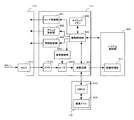
次に、主に信号処理チップ111の具体的な構成の一例について説明する。図5は、主に信号処理チップ111の具体的構成を示すブロック図である。
Next, an example of a specific configuration of the
信号処理チップ111は、分担化された制御機能としてのセンサ制御部441、ブロック制御部442、同期制御部443、信号制御部444と、これらの各制御部を統括制御する駆動制御部420とを含む。駆動制御部420は、撮像装置全体の統合制御を担うシステム制御部501からの指示を、各制御部が実行可能な制御信号に変換してそれぞれに引き渡す。
The
センサ制御部441は、撮像チップ113へ送出する、各画素の電荷蓄積、電荷読み出しに関わる制御パルスの送出制御を担う。具体的には、センサ制御部441は、対象画素に対してリセットパルスと転送パルスを送出することにより、電荷蓄積の開始と終了を制御し、読み出し画素に対して選択パルスを送出することにより、画素信号を出力配線309へ出力させる。
The
ブロック制御部442は、撮像チップ113へ送出する、制御対象となる単位グループ131を特定する特定パルスの送出を実行する。システム制御部501は、後述するように、被写界であるシーンの特性等に応じて撮像チップ113の画素領域を、それぞれが1つ以上の単位グループ131を含むように、複数のブロックに分割する。同一のブロックに含まれる画素は、同一の単位時間制御が実行される。すなわち、同一のブロックに含まれる画素は、一度の撮像指示に対して、同じ回数の電荷蓄積と画素信号出力を繰り返す。そこで、ブロック制御部442は、駆動制御部420からの指定に基づいて対象となる単位グループ131に特定パルスを送出することにより、単位グループ131をブロック化する役割を担う。各画素がTX配線307およびリセット配線306を介して受ける転送パルスおよびリセットパルスは、センサ制御部441が送出する各パルスとブロック制御部442が送出する特定パルスの論理積となる。駆動制御部420からの具体的なブロック化指定については、後に詳述する。
The
同期制御部443は、同期信号を撮像チップ113へ送出する。各パルスは、同期信号に同期して撮像チップ113においてアクティブとなる。例えば、同期信号を調整することにより、同一の単位グループ131に属する画素の特定画素のみを制御対象とするランダム制御、間引き制御等を実現する。
The
信号制御部444は、主にA/D変換器412bに対するタイミング制御を担う。出力配線309を介して出力された画素信号は、マルチプレクサ411を経てCDS回路412aおよびA/D変換器412bに入力される。A/D変換器412bは、信号制御部444によって制御されて、入力された画素信号をデジタル信号に変換する。デジタル信号に変換された画素信号は、演算回路415に引き渡され、後述の積算処理等が施される。積算処理等が施された画素信号は、メモリチップ112のデマルチプレクサ413に引き渡され、そしてそれぞれの画素に対応する画素メモリ414にデジタルデータの画素値として格納される。
The
信号処理チップ111は、いずれの単位グループ131を組み合わせてブロックを形成するかについてのブロック区分情報と、形成されたそれぞれのブロックが何回の電荷蓄積と画素信号出力を繰り返すかについての蓄積回数情報とを格納する、蓄積制御メモリとしてのタイミングメモリ430を有する。タイミングメモリ430は、例えばフラッシュRAMによって構成される。
The
後述するように、いずれの単位グループを組み合わせてブロックを形成するかについては、例えば、一連の撮影シーケンスに先立って実行されるシーンの輝度分布検出の検出結果に基づいて、システム制御部501により決定される。決定されたブロックは、例えば第1ブロック、第2ブロック…のように区分され、それぞれのブロックがいずれの単位グループ131を包含するかにより規定される。駆動制御部420は、このブロック区分情報をシステム制御部501から受け取り、タイミングメモリ430へ格納する。
As will be described later, which unit group is combined to form a block is determined by the
システム制御部501は、例えば、輝度分布の検出結果に基づいて、各ブロックが何回の電荷蓄積と画素信号出力を繰り返すかを決定する。駆動制御部420は、この繰り返し回数情報をシステム制御部501から受け取り、対応するブロック区分情報と対でタイミングメモリ430へ格納する。このようにタイミングメモリ430へブロック区分情報と繰り返し回数情報を格納することにより、駆動制御部420は、一連の電荷蓄積制御を、タイミングメモリ430を逐次参照して独立して実行し得る。すなわち、駆動制御部420は、1枚の画像取得制御において撮像指示の信号をシステム制御部501から一旦受け取ると、その後は各画素の制御についてその都度システム制御部501から指示を受けること無く、蓄積制御を完了させることができる。
For example, the
駆動制御部420は、更新されるブロック区分情報と繰り返し回数情報をシステム制御部501から受け取って、タイミングメモリ430の記憶内容を適宜更新する。例えば、駆動制御部420は、撮像準備指示または撮像指示に同期して、タイミングメモリ430を更新する。このように構成することにより、より高速な電荷蓄積制御を実現すると共に、駆動制御部420が電荷蓄積制御を実行している間に、システム制御部501は他の処理を並行して実行し得る。
The
駆動制御部420は、撮像チップ113に対する電荷蓄積制御を実行するに留まらず、読み出し制御の実行においてもタイミングメモリ430を参照する。例えば、駆動制御部420は、各ブロックの繰り返し回数情報を参照して、すでに画素メモリ414に格納されている画素信号を読み出し、演算回路415へ引き渡す。更には、演算回路415が演算処理を施した画素信号を、再度当該画素メモリ414に格納する。すなわち、画素メモリ414の画素信号を更新する。
The
また、駆動制御部420は、システム制御部501からの引渡要求に従って、対象画素信号を演算回路415およびデマルチプレクサ413を介して画素メモリ414から読み出し、撮像装置に設けられた画像処理部511へ引き渡す。画素メモリ414には、引渡要求に従って画素信号を伝送するデータ転送インタフェースが設けられている。データ転送インタフェースは、画像処理部511と繋がるデータ転送ラインと接続されている。データ転送ラインは例えばバスラインのうちのデータバスによって構成される。この場合、システム制御部501から駆動制御部420への引渡要求は、アドレスバスを利用したアドレス指定によって実行される。
Further, the
データ転送インタフェースによる画素信号の伝送は、アドレス指定方式に限らず、さまざまな方式を採用しうる。例えば、データ転送を行うときに、各回路の同期に用いられるクロック信号の立ち上がり・立ち下がりの両方を利用して処理を行うダブルデータレート方式を採用し得る。また、アドレス指定などの手順を一部省略することによってデータを一気に転送し、高速化を図るバースト転送方式を採用し得る。また、制御部、メモリ部、入出力部を並列に接続している回線を用いたバス方式、直列にデータを1ビットずつ転送するシリアル方式などを組み合わせて採用することもできる。 Transmission of pixel signals by the data transfer interface is not limited to the addressing method, and various methods can be adopted. For example, when performing data transfer, a double data rate method in which processing is performed using both rising and falling edges of a clock signal used for synchronization of each circuit may be employed. Further, it is possible to adopt a burst transfer method in which data is transferred all at once by omitting a part of the procedure such as addressing and the like, and the speed is increased. Further, a bus system using a line in which a control unit, a memory unit, and an input / output unit are connected in parallel, or a serial system that transfers data one bit at a time can be combined.
このように構成することにより、画像処理部511は、必要な画素信号に限って受け取ることができるので、特に低解像度の画像を形成する場合などにおいて、高速に画像処理を完了させることができる。また、演算回路415に積算処理を実行させる場合には、画像処理部511が積算処理を実行しなくて良いので、機能分担と並行処理により、画像処理の高速化を図ることができる。
With this configuration, the
図6は、本実施形態に係る撮像装置の構成を示すブロック図である。撮像装置500は、撮影光学系としての撮影レンズ520を備え、撮影レンズ520は、光軸Oに沿って入射する被写体光束を撮像素子100へ導く。撮影レンズ520は、撮像装置500に対して着脱できる交換式レンズであっても構わない。撮像装置500は、撮像素子100、システム制御部501、測光部503、ワークメモリ504、記録部505、および表示部506を主に備える。システム制御部501は、ユーザからの指示を受けて、撮像素子100へ送信する撮像指示を生成する撮像指示部の機能を担う。
FIG. 6 is a block diagram illustrating a configuration of the imaging apparatus according to the present embodiment. The imaging apparatus 500 includes a
撮影レンズ520は、複数の光学レンズ群から構成され、シーンからの被写体光束をその焦点面近傍に結像させる。なお、図6では瞳近傍に配置された仮想的な1枚のレンズで代表して表している。上述の通り、撮像素子100の駆動制御部420は、システム制御部501からの指示に従って撮像素子100のタイミング制御、領域制御等の電荷蓄積制御を実行する制御回路である。
The photographing
撮像素子100は、画素信号をシステム制御部501の画像処理部511へ引き渡す。画像処理部511は、ワークメモリ504をワークスペースとして種々の画像処理を施し、画像データを生成する。例えば、JPEGファイル形式の画像データを生成する場合は、ホワイトバランス処理、ガンマ処理等を施した後に圧縮処理を実行する。生成された画像データは、記録部505に記録されるとともに、表示信号に変換されて予め設定された時間の間、表示部506に表示される。なお、画像処理部511は、システム制御部501とは独立したASICとして構成されても良い。
The
測光部503は、画像データを生成する一連の撮影シーケンスに先立ち、シーンの輝度分布を検出する。測光部503は、例えば100万画素程度のAEセンサを含む。システム制御部501の演算部512は、測光部503の出力を受けてシーンの領域ごとの輝度を算出する。演算部512は、算出した輝度分布に従って上述の単位時間、絞り値、ISO感度を決定する。本実施形態において演算部512は、更に、撮像チップ113のどの画素グループ領域に決定した単位時間により何回の電荷蓄積と画素信号出力を繰り返させるかを決定する。また、演算部512は、最大の繰り返し回数が割り当てられた画素グループ領域の電荷蓄積が終了するまでの時間を計算して、シャッタの開閉タイミングを決定する。なお、演算部512は、撮像装置500を動作させるための各種演算も実行する。
The
図7は、シーンの例と領域分割を説明する図である。図7(a)は、撮像チップ113の画素領域が捉えるシーンを示す。具体的には、屋内環境に含まれるシャドウ被写体601および中間被写体602と、窓枠604の内側に観察される屋外環境のハイライト被写体603とが同時に写り込むシーンである。このような、ハイライト部からシャドウ部までの明暗差が大きなシーンを撮影する場合、従来の撮像素子であれば、ハイライト部を基準として電荷蓄積を実行するとシャドウ部で黒潰れが生じ、シャドウ部を基準として電荷蓄積を実行するとハイライト部で白飛びが生じた。すなわち、ハイライト部もシャドウ部も一律に一度の電荷蓄積により画像信号を出力させるには、明暗差の大きなシーンに対してフォトダイオードのダイナミックレンジが不足していると言える。そこで、本実施形態においては、シーンをハイライト部、シャドウ部といった部分領域に分割して、それぞれの領域に対応するフォトダイオードの電荷蓄積と画素信号読み出しの繰り返し回数を互いに異ならせることにより、ダイナミックレンジの実質的な拡大を図る。
FIG. 7 is a diagram for explaining an example of a scene and area division. FIG. 7A shows a scene captured by the pixel area of the
図7(b)は、撮像チップ113の画素領域における領域分割を示す。演算部512は、測光部503が捉えた図7(a)のシーンを解析して、輝度を基準に画素領域を分割する。例えば、システム制御部501は、測光部503に露光時間を変更しつつ複数回のシーン取得を実行させ、演算部512は、その白飛び領域、黒潰れ領域の分布の変化を参照して画素領域の分割ラインを決定する。図7(b)の例においては、演算部512は、シャドウ領域611、中間領域612、およびハイライト領域613の3領域に分割している。
FIG. 7B shows region division in the pixel region of the
分割ラインは、単位グループ131の境界に沿って定義される。すなわち、分割された各領域は、整数個の単位グループ131をそれぞれ含む。そして、同一の領域に包含される各グループの画素は、演算部512によって決定された単位時間による同一回数の電荷蓄積および画素信号出力を行う。属する領域が異なれば、異なる回数の電荷蓄積および画素信号出力を行う。
The division line is defined along the boundary of the
図8は、図7の例による分割された領域ごとの単位制御を説明する図である。ここでは、演算部512が、測光部503の出力を受けて、中間領域612のEV値とハイライト領域613のEV値との差が約1段分であり、また、シャドウ領域611のEV値と中間領域612のEV値との差が同じく約1段分であると算出した場合を説明する。
FIG. 8 is a diagram illustrating unit control for each divided area according to the example of FIG. Here, the
演算部512は、ユーザから撮影準備指示を受けると、測光部503の出力から1回あたりの電荷蓄積時間である共通の単位時間T0を決定する。ここでは、単位時間T0は、1回の電荷蓄積によりハイライト領域613の画素が飽和しないように、ハイライト領域613のEV値から決定される。例えば、ハイライト領域613の中でも最も明るい部分に対応する画素において、1回の電荷蓄積動作により蓄積可能な8割から9割の電荷が蓄積されることを基準として、単位時間T0が決定される。このとき、出力される画素信号の増幅率に相関するISO感度、および撮影レンズ520に設けられた絞りの絞り値は、演算部512により、決定された単位時間T0に応じて、ハイライト領域613が適正露出となるように算出される。なお、ISO感度は、全ての画素に共通に設定される。When the
演算部512は、算出したハイライト領域613のEV値と中間領域612のEV値の差を参照して、中間領域612の繰り返し回数を2回とする。すなわち、単位時間T0の電荷蓄積と、その電荷蓄積による画素信号読み出しを2回繰り返させる。同様に、演算部512は、算出したハイライト領域613のEV値とシャドウ領域611のEV値の差を参照して、シャドウ領域611の電荷蓄積回数を4回とする。すなわち、単位時間T0の電荷蓄積と、その電荷蓄積による画素信号読み出しを4回繰り返させる。後述するように、繰り返し読み出された画素信号は、演算回路415で順次足し合わされて画素メモリ414に格納される。The
ユーザから撮像指示を時刻t=0で受けると、駆動制御部420は、いずれの領域に属するグループの画素に対しても、リセットパルスと転送パルスを印加する。この印加をトリガーとして、いずれの画素も電荷蓄積を開始する。
When receiving an imaging instruction from the user at time t = 0, the
時刻t=T0となったら、駆動制御部420は、全ての画素に対して転送パルスを印加する。そして、各グループ内の画素に対して順次選択パルスを印加して、それぞれの画素信号を出力配線309に出力させる。駆動制御部420は、A/D変換器412bによりそれぞれの画素信号をデジタル信号に変換して、演算回路415を通過させ、それぞれ対応する画素メモリ414に格納する。この処理により、1回目の単位制御が完了する。そして、ハイライト領域613に属するグループの画素に対する処理を終了する。この時点で、ハイライト領域613の画素に対応する画素メモリ414に格納された画素信号から生成される画像は、白飛びおよび黒潰れがほとんど生じていない、PD104のダイナミックレンジを全体的に利用した適正露出の画像であることが期待できる。When time t = T 0 , the
全ての画素の画素信号を出力させたら、駆動制御部420は、中間領域612とシャドウ領域611に属するグループの画素に対して、時刻t=T0のタイミングで再びリセットパルスと転送パルスを印加して、2回目の電荷蓄積を開始させる。なお、画素信号の選択出力には時間を要するので、1回目の電荷蓄積の終了と2回目の電荷蓄積の開始の間には時間差が生じる。この時間差が実質的に無視し得ないのであれば、その時間分を遅延させて2回目の電荷蓄積を開始すれば良い。After outputting the pixel signals of all the pixels, the
時刻t=2T0となったら、駆動制御部420は、中間領域612とシャドウ領域611に属するグループの画素に対して転送パルスを印加する。そして、これらのグループ内の画素に対して順次選択パルスを印加して、それぞれの画素信号を出力配線309に出力させる。駆動制御部420は、A/D変換器412bによりそれぞれの画素信号をデジタル信号に変換する。これに並行して、それぞれ対応する既に画素メモリ414に格納された1回目の画素信号を読み出す。そして、駆動制御部420は、演算回路415に、1回目の画素信号と新たに取得した2回目の画素信号とを足し合わせる積算処理を実行させる。駆動制御部420は、積算処理により新たに生成された画素信号を、対応する画素メモリ414に格納する。これにより、それぞれの画素メモリ414は、1回目の画素信号から積算処理された画素信号に更新される。この処理により、2回目の単位制御が完了する。そして、中間領域612に属するグループの画素に対する処理を終了する。When time t = 2T 0 , the
この時点で、中間領域612の画素に対応する画素メモリ414に格納された画素信号から生成される画像は、白飛びおよび黒潰れがほとんど生じていない、画像データのビット幅を全体的に利用した適正露出の画像であることが期待できる。つまり、1回の単位制御では電荷蓄積時間が十分ではなく、黒潰れが生じがちなアンダー画像となってしまうところ、2回の単位制御を跨いで積算処理を施すことにより、実質的に2T0の期間の電荷蓄積を行ったのと同等の適正画像を得ることができる。さらには、電荷蓄積を2回に分けることにより、2T0の期間に渡る1回の電荷蓄積で得られる画像に比べ、ランダムノイズが低減することも期待できる。At this time, the image generated from the pixel signal stored in the
中間領域612とシャドウ領域611に属するグループの各画素の画素信号を出力させたら、駆動制御部420は、シャドウ領域611に属するグループの画素に対して、時刻t=2T0のタイミングで再びリセットパルスと転送パルスを印加して、3回目の電荷蓄積を開始させる。When the pixel signal of each pixel of the group belonging to the
時刻t=3T0となったら、駆動制御部420は、シャドウ領域611に属するグループの画素に対して転送パルスを印加する。そして、このグループ内の画素に対して順次選択パルスを印加して、それぞれの画素信号を出力配線309に出力させる。駆動制御部420は、A/D変換器412bによりそれぞれの画素信号をデジタル信号に変換する。これに並行して、それぞれ対応する既に画素メモリ414に格納された画素信号を読み出す。そして、駆動制御部420は、演算回路415に、読み出した画素信号と新たに取得した3回目の画素信号とを足し合わせる積算処理を実行させる。駆動制御部420は、積算処理により新たに生成された画素信号を、対応する画素メモリ414に格納する。これにより、それぞれの画素メモリ414は、新たに積算処理された画素信号に更新される。この処理により、3回目の単位制御が完了する。When time t = 3T 0 , the
続けて、駆動制御部420は、シャドウ領域611に属するグループの画素に対して、時刻t=3T0のタイミングで再びリセットパルスと転送パルスを印加して、4回目の電荷蓄積を開始させる。Subsequently, the
時刻t=4T0となったら、駆動制御部420は、シャドウ領域611に属するグループの画素に対して転送パルスを印加する。そして、このグループ内の画素に対して順次選択パルスを印加して、それぞれの画素信号を出力配線309に出力させる。駆動制御部420は、A/D変換器412bによりそれぞれの画素信号をデジタル信号に変換する。これに並行して、それぞれ対応する既に画素メモリ414に格納された画素信号を読み出す。そして、駆動制御部420は、演算回路415に、読み出した画素信号と新たに取得した4回目の画素信号とを足し合わせる積算処理を実行させる。駆動制御部420は、積算処理により新たに生成された画素信号を、対応する画素メモリ414に格納する。これにより、それぞれの画素メモリ414は、新たに積算処理された画素信号に更新される。この処理により、4回目の単位制御が完了する。そして、シャドウ領域611に属するグループの画素に対する処理を終了する。When time t = 4T 0 , the
この時点で、シャドウ領域611の画素に対応する画素メモリ414に格納された画素信号から生成される画像は、白飛びおよび黒潰れがほとんど生じていない、画像データのビット幅を全体的に利用した適正露出の画像であることが期待できる。つまり、1回の単位制御では電荷蓄積時間が十分ではなく、黒潰れが生じがちなアンダー画像となってしまうところ、4回の単位制御に跨いで積算処理を施すことにより、実質的に4T0の期間の電荷蓄積を行ったのと同等の適正画像を得ることができる。さらには、電荷蓄積を4回に分けることにより、4T0の期間に渡る1回の電荷蓄積で得られる画像に比べ、ランダムノイズが低減することも期待できる。At this time, the image generated from the pixel signal stored in the
システム制御部501は、4回目の電荷蓄積が終了するt=4T0のタイミングで、シャッタを閉じる。画像処理部511は、以上のように処理された各領域の画素信号を繋ぎ合わせて処理することにより、高ダイナミックレンジの画像データを生成する。The
なお、上記で説明した処理においては、駆動制御部420は、ある領域において予め定められた回数の単位制御が終了すると、他の領域が単位制御を継続している場合でも、その領域については、その後は電荷蓄積を実行しなかった。しかし、他の領域の単位制御に合わせて、その後も電荷蓄積を実行しても良い。この場合、転送パルスおよび選択パルスの印加による画素信号出力を行わなければ良い。あるいは、画素信号出力を行ったとしても、A/D変換器412bによるデジタル信号への変換、演算回路415による積算処理、画素メモリ414への格納等のいずれかの段階で画素信号を破棄する処理を行えば良い。
In the processing described above, when the unit control for a predetermined number of times in a certain region is completed, the
次に、一連の撮影動作処理について説明する。図9は、撮影動作の処理を示すフロー図である。フローは、撮像装置500の電源がONにされて開始される。 Next, a series of shooting operation processing will be described. FIG. 9 is a flowchart showing processing of the photographing operation. The flow is started when the power of the imaging apparatus 500 is turned on.
システム制御部501は、ステップS101で、撮像準備指示であるシャッタスイッチSW1の押し下げがなされるまで待機する。シャッタスイッチSW1の押し下げを検知したらステップS102へ進む。
In step S101, the
ステップS102では、システム制御部501は、測光処理を実行する。具体的には、測光部503の出力を得て、演算部512がシーンの輝度分布を算出する。そして、ステップS103へ進み、上述のように、単位時間、領域分割、繰り返し回数等を決定する。決定されたこれらの情報は、システム制御部501から駆動制御部420へ送られ、タイミングメモリ430で記憶される。
In step S102, the
撮像準備動作が完了したら、ステップS104へ進み、ユーザからの撮像指示であるシャッタスイッチSW2の押し下げがなされるまで待機する。このとき、経過時間が予め定められた時間Twを超えたら(ステップS105のYES)、ステップS101へ戻る。Twを超える前に(ステップS105のNO)スイッチSW2の押し下げを検知したら、ステップS106へ進む。 When the imaging preparation operation is completed, the process proceeds to step S104 and waits until the shutter switch SW2 that is an imaging instruction from the user is pressed down. At this time, if the elapsed time exceeds a predetermined time Tw (YES in step S105), the process returns to step S101. If the depression of the switch SW2 is detected before exceeding Tw (NO in step S105), the process proceeds to step S106.
駆動制御部420は、ステップS106において、1回目の単位制御として全画素による電荷蓄積を実行する。そして、単位時間の経過後に画素信号出力とA/D変換を実行し(ステップS107)、変換されたデジタル画素信号を、画素メモリ414に格納する(ステップS108)。
In step S106, the
続いて駆動制御部420は、ステップS109へ進み、2回目の単位制御を実行する対象領域を、タイミングメモリ430の領域分割情報を参照して決定する。そして、当該対象領域において電荷蓄積を実行する(ステップS110)。
Subsequently, the
駆動制御部420は、単位時間の経過後に2回目の電荷蓄積による画素信号出力とA/D変換を実行する(ステップS111)。これに並行して、あるいは前後して、駆動制御部420は、1回目の単位制御により格納された画素信号を画素メモリ414から読み出す(ステップS112)。そして、駆動制御部420は、演算回路415に、ステップS111でA/D変換された画素信号と、ステップS112で読み出された画素信号とを積算する積算処理を実行させる(ステップS113)。演算回路415によって積算された結果は、新たな画素信号として、ステップS112で読み出した画素メモリ414の値を更新して、格納される(ステップS114)。
The
駆動制御部420は、ステップS115へ進み、ステップS103で決定された繰り返し回数に到達したか否かを、タイミングメモリ430の繰り返し回数情報を参照して判断する。繰り返し回数に達していないと判断したら、ステップS109へ進み、3回目、4回目…の単位制御(ステップS109からステップS114)を実行する。繰り返し回数に達したと判断したら、ステップS116へ進む。
The
ステップS116では、駆動制御部420が単位制御の完了報告をシステム制御部501へ対して行い、これに応じて、システム制御部501は、駆動制御部420に対して画素メモリ414に格納された画素信号を画像処理部511へ送信させる。画像処理部511は画像処理を実行し例えばJPEG等の画像データを生成する。システム制御部501は、生成された画像データを記録部505に記録する記録処理を実行する。
In step S116, the
記録処理が完了したらステップS117へ進み、撮像装置500の電源がOFFにされたか否かを判断する。電源がOFFにされていないと判断したらステップS101へ戻り、OFFにされたと判断したら一連の撮影動作処理を終了する。 When the recording process is completed, the process proceeds to step S117, and it is determined whether or not the power of the imaging apparatus 500 has been turned off. If it is determined that the power has not been turned off, the process returns to step S101.
なお、上記で説明した処理においては、駆動制御部420は、単位時間T0を、ハイライト領域613の画素が飽和しない時間として決定した。ハイライト領域613は、測光部503の測光結果に基づいて決定されるので、駆動制御部420は、図9のフローを用いて説明したような撮像タイミングに合わせて、単位時間T0をその都度決定している。しかし、単位時間T0は、撮影ごとに動的に変更するのでは無く、予め定められた固定値を採用することもできる。In the processing described above, the
例えば、固定値としてT0=1/256秒を採用した場合の、図8のシーンに対する単位制御を考える。システム制御部501は、測光結果として、ハイライト領域613を適正露出とする電荷蓄積時間を1/64秒、中間領域612を適正露出とする電荷蓄積時間を1/32秒、シャドウ領域611を適正露出とする電荷蓄積時間を1/16秒と算出した場合を想定する。この場合、ハイライト領域613に対しては、(1/64)÷(1/256)=4回、中間領域612に対しては、(1/32)÷(1/256)=8回、シャドウ領域611に対しては、(1/16)÷(1/256)=16回の繰り返し回数を決定すれば良い。For example, consider unit control for the scene of FIG. 8 when T 0 = 1/256 seconds is adopted as a fixed value. As a photometric result, the
ここで、固定値としての単位時間T0は、これより短時間の電荷蓄積を行えないことになるので、明るいシーンに対しても単位時間制御が行えるように、比較的短い時間に設定することが好ましい。ただし、本実施形態においてはA/D変換後のデジタルの画素信号で積算処理を実行するので、単位時間T0の電荷蓄積によりシャドウ部においても1以上の値を持つように、A/D変換器412bの量子化ビット数を増やしておくべきである。この場合、画素メモリ414も、当該量子化ビット数に合わせて格納サイズが設定される。ここで、画像処理部511で処理されるビット数と画素メモリ414に格納される画素信号のビット数が異なる場合は、システム制御部501からの引渡要求に同期して、演算回路415によりビット変換を行った後に画素信号を画像処理部511へ引き渡せば良い。Here, since the unit time T 0 as a fixed value cannot be stored for a shorter time than this, the unit time T 0 should be set to a relatively short time so that the unit time can be controlled even for a bright scene. Is preferred. However, in this embodiment, since the integration process is executed with the digital pixel signal after A / D conversion, the A / D conversion is performed so that the shadow portion has a value of 1 or more due to the charge accumulation of unit time T 0. The number of quantization bits of the
さらに、測光部503の測光結果を利用すること無く、単位制御を実行することもできる。具体的には、画素メモリ414から画素信号を読み出して単位グループごとの平均値、あるいは、隣接する単位グループも含めた例えば縦横5×5=25グループごとの平均値を逐次算出しつつ、これが閾値を超えたか否かにより、更なる単位制御を行うか否かを決定する。すなわち、単位制御を繰り返した結果、明るい画像となったと考えられる領域はそれ以上の単位制御を行わず、まだ暗い画像であると考えられる領域は更なる単位制御を続ける。このような平均値判断を行うことによっても、それぞれの領域の画像を適正露出に近い画像とすることができる。この場合、画素メモリ414に格納された画素信号を画像処理部511へ引き渡すときには、繰り返し回数で正規化すれば良い。具体的には、例えばそれぞれの画素信号を繰り返し回数で割った値とすれば良い。なお、閾値を超えたか否かの判断を行う対象となる値は、平均値に限らず、さまざまな統計処理により算出された算出値を利用することができる。
Furthermore, unit control can be performed without using the photometric result of the
本実施形態における撮像装置500の構成によれば、領域ごとに適正露出にすべく単位制御を実行するに留まらず、さまざまな画像効果との関係において単位制御を実行することができる。例えば、単位時間T0を、手振れが生じにくい比較的短い時間に設定しておき、像ずれが許容量を超えるまで単位制御の繰り返しを実行することができる。この場合、像ずれ量の検出は動作検出部の検出結果を用いることができる。動作検出部は、例えば測光センサの出力を利用するのであれば測光部503が担うこともできるし、別途設けられた他の動き検出センサが担うこともできる。このような単位時間制御によれば、像振れの少ない画像を得ることができる。なお、予定された電荷蓄積時間に到達しないことによる明るさの不足分は、画素信号を増幅することにより調整すれば良い。According to the configuration of the imaging apparatus 500 in the present embodiment, unit control can be executed in relation to various image effects, in addition to executing unit control to achieve appropriate exposure for each region. For example, the unit time T 0 can be set to a relatively short time in which camera shake is unlikely to occur, and the unit control can be repeated until the image shift exceeds an allowable amount. In this case, the detection result of the motion detection unit can be used to detect the image shift amount. For example, if the output of the photometric sensor is used, the motion detection unit can be used by the
また、領域ごとに排他的に単位制御を実行することもできる。例えば図8の例において、1回目の単位制御はハイライト領域613に対してのみを行い、続く2回目と3回目の単位制御は中間領域612に対してのみ行い、続く4回目から7回目の単位制御はシャドウ領域611に対してのみを行うことができる。このように領域ごとに排他的に単位制御を実行すれば、例えば領域ごとに絞り値などの光学条件を変更した、多彩な画像を取得することができる。より具体的には、滝の流れる領域に対しては絞りを絞って単位制御をより多く繰り返し、その周辺に存在する木々の領域に対しては絞りを開いて少ない単位制御を実行することができる。このような制御によれば、1枚の画像の中に異なるシャッタ速度の像を共存させることができるので、従来に無い画像を一度の撮像指示により取得することができる。なお、例えばライブビュー画像を通じてユーザから予め指示を受け付ければ、シーンのどの領域に何回の単位制御を繰り返させるかを事前に定めることができる。
In addition, unit control can be executed exclusively for each area. For example, in the example of FIG. 8, the first unit control is performed only for the
以上説明した各実施形態においては、静止画像を前提として説明したが、もちろんフレームごとに同様の単位制御をおこなうことにより、動画像を生成することもできる。また、デジタルカメラ専用機に限らず、もちろん携帯電話、情報端末、PC等の電子機器に組み込まれたカメラユニットに対しても上述の処理を実行させることができる。 In each of the embodiments described above, a description has been given on the premise of a still image. However, a moving image can also be generated by performing similar unit control for each frame. In addition, the above-described processing can be executed not only on a digital camera dedicated machine, but also on a camera unit incorporated in an electronic device such as a mobile phone, an information terminal, or a PC.
さらにバリエーションについて説明する。図10は、別実施例としての、分割された領域ごとの電荷蓄積制御を説明する図である。ここでは、図8の例と同様に、演算部512が、測光部503の出力を受けて、中間領域612のEV値とハイライト領域613のEV値との差が約1段分であり、また、シャドウ領域611のEV値と中間領域612のEV値との差が同じく約1段分であると算出した場合を説明する。演算部512は、ユーザから撮影準備指示を受けると、図8の例と同様に、測光部503の出力から1回あたりの電荷蓄積時間である共通の単位時間T0を決定する。Further variations will be described. FIG. 10 is a diagram for explaining charge accumulation control for each divided area as another embodiment. Here, as in the example of FIG. 8, the
演算部512は、算出したハイライト領域613のEV値と中間領域612のEV値の差を参照して、中間領域612において必要な電荷蓄積回数を2回と決定する。同様に、演算部512は、算出したハイライト領域613のEV値とシャドウ領域611のEV値の差を参照して、シャドウ領域611において必要な電荷蓄積回数を4回と決定する。ここで、本実施例においては、シャドウ領域611において決定された、すなわち必要と決定された電荷蓄積回数の最大値である4回を、全領域における電荷蓄積回数とする。つまり、ハイライト領域613、中間領域612、シャドウ領域611の全領域において、単位時間T0の電荷蓄積と、その電荷蓄積による画素信号読み出しを4回繰り返させる。The
ユーザから撮像指示を時刻t=0で受けると、駆動制御部420は、いずれの領域に属するグループの画素に対しても、リセットパルスと転送パルスを印加する。この印加をトリガーとして、いずれの画素も電荷蓄積を開始する。
When receiving an imaging instruction from the user at time t = 0, the
時刻t=T0となったら、駆動制御部420は、全ての画素に対して転送パルスを印加する。そして、各グループ内の画素に対して順次選択パルスを印加して、それぞれの画素信号を出力配線309に出力させる。駆動制御部420は、A/D変換器412bによりそれぞれの画素信号をデジタル信号に変換して、演算回路415を通過させ、それぞれ対応する画素メモリ414に格納する。この処理により、1回目の単位制御が完了する。When time t = T 0 , the
全ての画素の画素信号を出力させたら、駆動制御部420は、再び全領域の画素に対して、時刻t=T0のタイミングで再びリセットパルスと転送パルスを印加して、2回目の電荷蓄積を開始させる。なお、画素信号の選択出力には時間を要するので、1回目の電荷蓄積の終了と2回目の電荷蓄積の開始の間には時間差が生じる。この時間差が実質的に無視し得ないのであれば、その時間分を遅延させて2回目の電荷蓄積を開始すれば良い。After outputting the pixel signals of all the pixels, the
時刻t=2T0となったら、駆動制御部420は、全ての画素に対して転送パルスを印加する。そして、各グループ内の画素に対して順次選択パルスを印加して、それぞれの画素信号を出力配線309に出力させる。駆動制御部420は、A/D変換器412bによりそれぞれの画素信号をデジタル信号に変換する。これに並行して、それぞれ対応する既に画素メモリ414に格納された1回目の画素信号を読み出す。そして、駆動制御部420は、演算回路415に、1回目の画素信号と新たに取得した2回目の画素信号とを足し合わせる積算処理を実行させる。駆動制御部420は、積算処理により新たに生成された画素信号を、対応する画素メモリ414に格納する。これにより、それぞれの画素メモリ414は、1回目の画素信号から積算処理された画素信号に更新される。この処理により、2回目の単位制御が完了する。When time t = 2T 0 , the
同様に、時刻t=2T0から3T0の間に3回目の電荷蓄積および画素信号読み出しを行い、時刻t=3T0から4T0の間に4回目の電荷蓄積および画素信号読み出しを行う。4回目の積算処理が終了した時点で、ハイライト領域613においては、1回の電荷蓄積で足りるところを4回繰り返しているので、積算処理した画素信号の値を1/4とする演算を行う。単位時間T0は、上述のように、ハイライト領域613の中でも最も明るい部分に対応する画素において、1回の電荷蓄積動作により蓄積可能な8割から9割の電荷が蓄積されることを基準として定められているので、それぞれの電荷蓄積において飽和することはない。したがって、積算処理した画素信号の値を1/4にして得られるハイライト領域613の画像は、白飛びおよび黒潰れがほとんど生じていない、PD104のダイナミックレンジを全体的に利用した適正露出の画像であることが期待できる。Similarly, the third charge accumulation and pixel signal readout are performed between time t = 2T 0 and 3T 0 , and the fourth charge accumulation and pixel signal readout are performed between time t = 3T 0 and 4T 0 . At the end of the fourth integration process, in the
同様に、4回目の積算処理が終了した時点で、中間領域612においては、2回の電荷蓄積で足りるところを4回繰り返しているので、積算処理した画素信号の値を1/2とする演算を行う。積算処理した画素信号の値を1/2にして得られる中間領域612の画像は、白飛びおよび黒潰れがほとんど生じていない、画像データのビット幅を全体的に利用した適正露出の画像であることが期待できる。
Similarly, at the time when the fourth integration process is completed, in the
また、4回積算処理した画素信号から得られるシャドウ領域611の画像は、白飛びおよび黒潰れがほとんど生じていない、画像データのビット幅を全体的に利用した適正露出の画像であることが期待できる。つまり、1回の単位制御では電荷蓄積時間が十分ではなく、黒潰れが生じがちなアンダー画像となってしまうところ、4回の単位制御に跨いで積算処理を施すことにより、実質的に4T0の期間の電荷蓄積を行ったのと同等の適正画像を得ることができる。Also, the image of the
本実施例におけるこのような電荷蓄積制御を行うと、4T0の期間の間に被写体が領域間を跨いで移動するような場合でも、領域の境界において被写体像が不連続となるような不自然な画像にはならない。例えば、太陽光が車体の一部に当たった移動する自動車を撮影する場合でも、撮影画像において輝点の軌跡が領域間で途切れることがない。When such charge accumulation control is performed in the present embodiment, even when the subject moves across regions during the period of 4T 0 , the subject image becomes unnatural at the boundary of the region. It will not be a good image. For example, even when shooting a moving automobile in which sunlight hits a part of a vehicle body, the locus of bright spots does not break between regions in the captured image.
なお、以上の制御においては、すべての積算処理を終えてから、ハイライト領域613では1/4とし、中間領域612では1/2とする演算を行った。しかし、それぞれの画素信号をデジタル信号に変換して、それぞれに対応する画素メモリ414に格納する段階において、演算回路415が、ハイライト領域613の画素に対しては1/4とし、中間領域612の画素に対しては1/2とする演算を行っても良い。つまり、各回の画素信号読み出し処理において、領域ごとに低減演算を行っても良い。このように処理しても、上記と同様の効果が得られる。
In the above control, after all the integration processes have been completed, the calculation is performed such that the
さらに別のバリエーションについて説明する。図8を用いて説明した実施例においては、システム制御部501は、測光部503の出力からシーンの輝度分布を算出して、単位時間T0、領域分割、繰り返し回数を決定した。しかし、測光部503の出力結果を得なくても、これらを決定することができる。Still another variation will be described. In the embodiment described with reference to FIG. 8, the
システム制御部501は、例えば、ビューファインダとして用いていたライブビュー画像から単位時間T0を決める。このとき、ハイライト部が白飛びしないように、ライブビュー画像を取得するためのシャッタ速度よりも短い時間とすると良い。そして、ユーザから撮像指示であるシャッタスイッチSW2の押し下げ操作を受けたら、システム制御部501は、まず1回目の電荷蓄積および画素信号読み出しを行う。そして、ここで得られた画素信号のレベルを解析して、領域を分割し、その分割された領域ごとの電荷蓄積の繰り返し回数を決定する。具体的には、例えば、蓄積可能な50%以上の電荷が蓄積された画素が多数を占める領域を1回の蓄積制御で終了する領域と定め、25%以上50%未満の電荷が蓄積された画素が多数を占める領域を2回の蓄積制御で終了する領域と定め、25%未満の電荷が蓄積された画素が多数を占める領域を4回の蓄積制御で終了する領域と定める。そして、2回目以降の電荷蓄積および画素信号読み出しを継続して実行する。このように制御すれば、測光部503を独立して設けなくても良い。あるいは、撮影モードの特性に合わせて、測光部503の出力を用いた制御とこのような制御を切り替えることもできる。For example, the
あるいは、システム制御部501は、1回目の電荷蓄積および画素信号読み出しにおいては領域分割までを実行し、それぞれの領域ごとに次の電荷蓄積および画素信号読み出しを行うか否かを各回の信号読み出し後に判断するように制御することもできる。すなわち、システム制御部501は、ある領域においてm(自然数)回の電荷蓄積および画素信号読み出しが終了した時に、積算処理後の画素信号の値が予め定められた範囲に入っていればm+1回目の電荷蓄積を行わず終了し、入っていなければm+1回目の電荷蓄積を実行する。また、別の領域においてn(自然数)回の電荷蓄積および画素信号読み出しが終了した時に、積算処理後の画素信号の値が予め定められた範囲に入っていればn+1回目の電荷蓄積を行わず終了し、入っていなければn+1回目の電荷蓄積を実行する。
Alternatively, the
また上述において、測光部503の測光結果を用いず、単位グループごとの平均値等を逐次算出しつつ、これが閾値を超えたか否かにより、更なる単位制御を行うか否かを決定する例を説明したが、この制御において閾値を蓄積回数に応じて変更しても良い。具体的には、蓄積回数が増えるに従って、閾値を徐々に小さくする。閾値を徐々に小さくすることにより、シャドウ領域とハイライト領域の明るさが逆転することのない、自然な画像を生成することができる。
Further, in the above description, an example in which whether or not to perform further unit control is determined by sequentially calculating an average value or the like for each unit group without using the photometric result of the
以上、本発明を実施の形態を用いて説明したが、本発明の技術的範囲は上記実施の形態に記載の範囲には限定されない。上記実施の形態に、多様な変更または改良を加えることが可能であることが当業者に明らかである。その様な変更または改良を加えた形態も本発明の技術的範囲に含まれ得ることが、請求の範囲の記載から明らかである。 As mentioned above, although this invention was demonstrated using embodiment, the technical scope of this invention is not limited to the range as described in the said embodiment. It will be apparent to those skilled in the art that various modifications or improvements can be added to the above-described embodiment. It is apparent from the scope of the claims that the embodiments added with such changes or improvements can be included in the technical scope of the present invention.
請求の範囲、明細書、および図面中において示した装置、システム、プログラム、および方法における動作、手順、ステップ、および段階等の各処理の実行順序は、特段「より前に」、「先立って」等と明示しておらず、また、前の処理の出力を後の処理で用いるのでない限り、任意の順序で実現しうることに留意すべきである。請求の範囲、明細書、および図面中の動作フローに関して、便宜上「まず、」、「次に、」等を用いて説明したとしても、この順で実施することが必須であることを意味するものではない。 The execution order of each process such as operations, procedures, steps, and stages in the apparatus, system, program, and method shown in the claims, the description, and the drawings is particularly “before” or “prior”. It should be noted that they can be implemented in any order unless the output of the previous process is used in the subsequent process. Regarding the operation flow in the claims, the description, and the drawings, even if it is described using “first”, “next”, etc. for the sake of convenience, it means that it is essential to carry out in this order. is not.
100 撮像素子、101 マイクロレンズ、102 カラーフィルタ、103 パッシベーション膜、104 PD、105 トランジスタ、106 PD層、107 配線、108 配線層、109 バンプ、110 TSV、111 信号処理チップ、112 メモリチップ、113 撮像チップ、131 単位グループ、302 転送トランジスタ、303 リセットトランジスタ、304 増幅トランジスタ、305 選択トランジスタ、306 リセット配線、307 TX配線、308 デコーダ配線、309 出力配線、310 Vdd配線、311 負荷電流源、411 マルチプレクサ、412 信号処理回路、413 デマルチプレクサ、414 画素メモリ、415 演算回路、420 駆動制御部、430 タイミングメモリ、441 センサ制御部、442 ブロック制御部、443 同期制御部、444 信号制御部、500 撮像装置、501 システム制御部、503 測光部、504 ワークメモリ、505 記録部、506 表示部、511 画像処理部、512 演算部、601 シャドウ被写体、602 中間被写体、603 ハイライト被写体、604 窓枠、611 シャドウ領域、612 中間領域、613 ハイライト領域 100 imaging device, 101 microlens, 102 color filter, 103 passivation film, 104 PD, 105 transistor, 106 PD layer, 107 wiring, 108 wiring layer, 109 bump, 110 TSV, 111 signal processing chip, 112 memory chip, 113 imaging Chip, 131 unit group, 302 transfer transistor, 303 reset transistor, 304 amplification transistor, 305 selection transistor, 306 reset wiring, 307 TX wiring, 308 decoder wiring, 309 output wiring, 310 Vdd wiring, 311 load current source, 411 multiplexer, 412 Signal processing circuit, 413 demultiplexer, 414 pixel memory, 415 arithmetic circuit, 420 drive control unit, 430 timing memory, 441 Sensor control unit, 442 block control unit, 443 synchronization control unit, 444 signal control unit, 500 imaging device, 501 system control unit, 503 photometry unit, 504 work memory, 505 recording unit, 506 display unit, 511 image processing unit, 512 Calculation unit, 601 shadow subject, 602 intermediate subject, 603 highlight subject, 604 window frame, 611 shadow region, 612 intermediate region, 613 highlight region
Claims (95)
少なくとも1つの画素を含む前記第1画素グループとは異なる第2画素グループと、
前記第1画素グループに含まれる前記画素においてm(mは自然数)回の電荷蓄積により得られた第1画素信号に基づいて、前記第1画素グループに含まれる前記画素においてm+1回目の電荷蓄積を行うように制御し、前記第2画素グループに含まれる前記画素においてn(nは自然数)回の電荷蓄積により得られた第2画素信号に基づいて、前記第2画素グループに含まれる前記画素においてn+1回目の電荷蓄積を行うように制御する制御部と、
を備える撮像ユニット。 A first pixel group including at least one pixel;
A second pixel group different from the first pixel group including at least one pixel;
Based on a first pixel signal obtained by m (m is a natural number) charge accumulation in the pixels included in the first pixel group, m + 1 charge accumulation is performed in the pixels included in the first pixel group. The pixel included in the second pixel group is controlled based on the second pixel signal obtained by n (n is a natural number) charge accumulation in the pixel included in the second pixel group. a control unit that controls to perform the (n + 1) th charge accumulation;
An imaging unit comprising:
前記第2画素信号が格納される第2格納部と、
前記第1格納部に格納されている前記第1画素信号と、前記第1画素グループに含まれる前記画素においてm+1回目の電荷蓄積を行うことにより得られた画素信号と、により第1信号を生成する第1信号処理部と、
前記第2格納部に格納されている前記第2画素信号と、前記第2画素グループに含まれる前記画素においてn+1回目の電荷蓄積を行うことにより得られた画素信号と、により第2信号を生成する第2信号処理部と、
を備える請求項1から請求項3のいずれか一項に記載の撮像ユニット。 A first storage for storing the first pixel signal;
A second storage for storing the second pixel signal;
A first signal is generated from the first pixel signal stored in the first storage unit and a pixel signal obtained by performing m + 1th charge accumulation in the pixels included in the first pixel group. A first signal processing unit,
A second signal is generated based on the second pixel signal stored in the second storage unit and the pixel signal obtained by performing the (n + 1) th charge accumulation in the pixels included in the second pixel group. A second signal processing unit,
The imaging unit according to any one of claims 1 to 3, further comprising:
前記第2画素グループの画素は、光を電荷に変換する第2光電変換部を有する請求項1から請求項6のいずれか一項に記載の撮像ユニット。 The pixels of the first pixel group have a first photoelectric conversion unit that converts light into electric charge,
7. The imaging unit according to claim 1, wherein the pixels of the second pixel group include a second photoelectric conversion unit that converts light into electric charge.
前記第2画素グループの画素は、前記第2光電変換部の電荷を転送するための第2転送部を有し、
前記第1転送部に接続され、前記第1転送部を制御するための制御信号が出力される第1転送配線と、
前記第2転送部に接続され、前記第2転送部を制御するための制御信号が出力される第2転送配線と、
を備える請求項7に記載の撮像ユニット。 The pixels of the first pixel group have a first transfer unit for transferring charges of the first photoelectric conversion unit,
The pixels of the second pixel group have a second transfer unit for transferring charges of the second photoelectric conversion unit,
A first transfer wiring connected to the first transfer unit and outputting a control signal for controlling the first transfer unit;
A second transfer wiring connected to the second transfer unit and outputting a control signal for controlling the second transfer unit;
An imaging unit according to claim 7.
前記第2画素グループの画素は、前記第2光電変換部からの電荷が転送される第2フローティングディフュージョンの電位をリセットする第2リセット部を有し、
前記第1リセット部に接続され、前記第1リセット部を制御するための制御信号が出力される第1リセット配線と、
前記第2リセット部に接続され、前記第2リセット部を制御するための制御信号が出力される第2リセット配線と、
を備える請求項7又は請求項8に記載の撮像ユニット。 The pixels of the first pixel group include a first reset unit that resets a potential of a first floating diffusion to which charges from the first photoelectric conversion unit are transferred,
The pixels of the second pixel group have a second reset unit that resets the potential of the second floating diffusion to which the charge from the second photoelectric conversion unit is transferred,
A first reset wiring connected to the first reset unit and outputting a control signal for controlling the first reset unit;
A second reset wiring connected to the second reset unit and outputting a control signal for controlling the second reset unit;
The imaging unit according to claim 7 or 8, comprising:
前記第2画素グループは、複数の前記画素を有する請求項1から請求項8のいずれか一項に記載の撮像ユニット。 The first pixel group includes a plurality of the pixels,
The imaging unit according to any one of claims 1 to 8, wherein the second pixel group includes a plurality of the pixels.
複数の前記第2画素グループと、
を備える請求項1から請求項11のいずれか一項に記載の撮像ユニット。 A plurality of the first pixel groups;
A plurality of the second pixel groups;
The imaging unit according to claim 1, further comprising:
前記制御部は、前記撮像チップとは異なる半導体チップに配置されている請求項1から請求項12のいずれか一項に記載の撮像ユニット。 The first pixel group and the second pixel group are disposed on an imaging chip,
The imaging unit according to any one of claims 1 to 12, wherein the control unit is arranged on a semiconductor chip different from the imaging chip.
前記画素において蓄積された電荷に基づく第1画素信号が格納される格納部と、
前記格納部に格納されている前記第1画素信号と、前記画素において前記第1画素信号が生成された後に電荷蓄積を実行して生成された第2画素信号と、により生成された信号を前記格納部に格納する信号処理を行う信号処理部と、
前記複数の画素グループの画素グループごとに前記信号処理を前記信号処理部に実行させるか否かを制御する制御部と、
を備える撮像ユニット。 A plurality of pixel groups including at least one pixel capable of performing charge accumulation a plurality of times in response to an imaging instruction for generating one frame of image data;
A storage unit for storing a first pixel signal based on charges accumulated in the pixel;
A signal generated by the first pixel signal stored in the storage unit and a second pixel signal generated by performing charge accumulation after the first pixel signal is generated in the pixel is the signal A signal processing unit for performing signal processing to be stored in the storage unit;
A control unit that controls whether or not to cause the signal processing unit to execute the signal processing for each pixel group of the plurality of pixel groups;
An imaging unit comprising:
前記信号処理部は、前記撮像チップとは異なる信号処理チップに配置されている請求項15に記載の撮像ユニット。 The plurality of pixel groups are arranged on an imaging chip,
The imaging unit according to claim 15, wherein the signal processing unit is arranged in a signal processing chip different from the imaging chip.
前記格納部は、前記撮像チップとは異なるメモリチップに配置されている請求項15に記載の撮像ユニット。 The pixel group is disposed on an imaging chip,
The imaging unit according to claim 15, wherein the storage unit is arranged in a memory chip different from the imaging chip.
を備える請求項25に記載の電子機器。 An image processing unit connected to the storage unit and generating image data;
An electronic apparatus according to claim 25.
光を電荷に変換する第2光電変換部と、
前記第1光電変換部においてm(mは自然数)回の電荷蓄積を行って得られた第1信号に基づいて、前記第1光電変換部においてm+1回目の電荷蓄積を行うように制御し、前記第2光電変換部においてn(nは自然数)回の電荷蓄積を行って得られた第2信号に基づいて、前記第2光電変換部においてn+1回目の電荷蓄積を行うように制御する制御部と、
を備える撮像ユニット。 A first photoelectric conversion unit that converts light into electric charge;
A second photoelectric conversion unit that converts light into electric charge;
Based on the first signal obtained by performing the charge accumulation m (m is a natural number) times in the first photoelectric conversion unit, the first photoelectric conversion unit is controlled to perform the (m + 1) th charge accumulation, A control unit that controls to perform the (n + 1) th charge accumulation in the second photoelectric conversion unit based on a second signal obtained by performing n (n is a natural number) charge accumulation in the second photoelectric conversion unit; ,
An imaging unit comprising:
前記第2信号が格納される第2格納部と、を備え、
前記制御部は、前記第1格納部に格納された前記第1信号に基づいて、前記第1光電変換部において前記m+1回目の電荷蓄積を行うように制御し、前記第2格納部に格納された前記第2信号に基づいて、前記第2光電変換部において前記n+1回目の電荷蓄積を行うように制御する請求項27に記載の撮像ユニット。 A first storage for storing the first signal;
A second storage unit in which the second signal is stored,
The control unit controls the first photoelectric conversion unit to perform the (m + 1) th charge accumulation based on the first signal stored in the first storage unit, and is stored in the second storage unit. 28. The imaging unit according to claim 27, wherein control is performed so that the (n + 1) th charge accumulation is performed in the second photoelectric conversion unit based on the second signal.
前記第2格納部に格納された前記第2信号を用いて演算を行う第2演算回路と、を備え、
前記制御部は、前記第1演算回路の演算結果により、前記第1光電変換部において前記m+1回目の電荷蓄積を行うように制御し、前記第2演算回路の演算結果により、前記第2光電変換部において前記n+1回目の電荷蓄積を行うように制御する請求項28に記載の撮像ユニット。 A first arithmetic circuit that performs an operation using the first signal stored in the first storage unit;
A second arithmetic circuit that performs an operation using the second signal stored in the second storage unit,
The control unit controls the first photoelectric conversion unit to perform the (m + 1) th charge accumulation according to the calculation result of the first calculation circuit, and the second photoelectric conversion according to the calculation result of the second calculation circuit. 29. The imaging unit according to claim 28, wherein control is performed so that the (n + 1) th charge accumulation is performed in a unit.
前記第2演算回路は、前記第2格納部に格納された前記第2信号と、前記n+1回目の電荷蓄積により得られる第5信号と、により第6信号を生成する請求項31に記載の撮像ユニット。 The first arithmetic circuit generates a fourth signal from the first signal stored in the first storage unit and the third signal obtained by the m + 1th charge accumulation,
32. The imaging according to claim 31, wherein the second arithmetic circuit generates a sixth signal from the second signal stored in the second storage unit and a fifth signal obtained by the n + 1-th charge accumulation. unit.
前記第2演算回路は、前記第2格納部に格納された前記第2信号と、前記第5信号と、を用いて信号処理を行って前記第6信号を生成する請求項32に記載の撮像ユニット。 The first arithmetic circuit performs signal processing using the first signal stored in the first storage unit and the third signal to generate the fourth signal,
The imaging according to claim 32, wherein the second arithmetic circuit performs signal processing using the second signal stored in the second storage unit and the fifth signal to generate the sixth signal. unit.
前記第2格納部は、前記第2演算回路により生成された前記第6信号が格納される請求項32又は請求項33に記載の撮像ユニット。 The first storage unit stores the fourth signal generated by the first arithmetic circuit,
The imaging unit according to claim 32 or 33, wherein the second storage unit stores the sixth signal generated by the second arithmetic circuit.
前記第2格納部は、前記第2信号に置き換えて前記第6信号が格納される請求項34に記載の撮像ユニット。 The first storage unit stores the fourth signal in place of the first signal,
The imaging unit according to claim 34, wherein the second storage unit stores the sixth signal in place of the second signal.
前記第1格納部及び前記第2格納部は、前記第1半導体チップとは異なる第2半導体チップに配置される請求項28から請求項35のいずれか一項に記載の撮像ユニット。 The first photoelectric conversion unit and the second photoelectric conversion unit are disposed on a first semiconductor chip,
36. The imaging unit according to any one of claims 28 to 35, wherein the first storage unit and the second storage unit are disposed on a second semiconductor chip different from the first semiconductor chip.
アナログ信号をデジタル信号に変換するための第2変換部と、を備え、
前記第1格納部は、前記第1変換部を用いてデジタル信号に変換された前記第1信号が格納され、
前記第2格納部は、前記第2変換部を用いてデジタル信号に変換された前記第2信号が格納される請求項28から請求項37のいずれか一項に記載の撮像ユニット。 A first converter for converting an analog signal into a digital signal;
A second converter for converting an analog signal into a digital signal,
The first storage unit stores the first signal converted into a digital signal using the first conversion unit,
38. The imaging unit according to any one of claims 28 to 37, wherein the second storage unit stores the second signal converted into a digital signal using the second conversion unit.
前記第1格納部及び前記第2格納部は、前記第1半導体チップとは異なる第2半導体チップに配置され、
前記第1変換部及び前記第2変換部は、前記第1半導体チップ及び前記第2半導体チップとは異なる第3半導体チップに配置される請求項38に記載の撮像ユニット。 The first photoelectric conversion unit and the second photoelectric conversion unit are disposed on a first semiconductor chip,
The first storage unit and the second storage unit are disposed on a second semiconductor chip different from the first semiconductor chip,
39. The imaging unit according to claim 38, wherein the first conversion unit and the second conversion unit are arranged on a third semiconductor chip different from the first semiconductor chip and the second semiconductor chip.
前記第2光電変換部の電荷を転送する第2転送部と、を備え、
前記制御部は、前記m+1回目の電荷蓄積を行うように前記第1転送部を制御し、前記n+1回目の電荷蓄積を行うように前記第2転送部を制御する請求項27から請求項40のいずれか一項に記載の撮像ユニット。 A first transfer unit that transfers charges of the first photoelectric conversion unit;
A second transfer unit that transfers the charge of the second photoelectric conversion unit,
41. The control unit according to claim 27, wherein the control unit controls the first transfer unit to perform the m + 1th charge accumulation and controls the second transfer unit to perform the n + 1th charge accumulation. The imaging unit according to any one of the above.
前記第2光電変換部からの電荷が転送される第2フローティングディフュージョンの電位をリセットする第2リセット部と、を備え、
前記制御部は、前記m+1回目の電荷蓄積を行うように前記第1リセット部を制御し、前記n+1回目の電荷蓄積を行うように前記第2リセット部を制御する請求項27から請求項41のいずれか一項に記載の撮像ユニット。 A first reset unit for resetting a potential of the first floating diffusion to which charges from the first photoelectric conversion unit are transferred;
A second reset unit that resets the potential of the second floating diffusion to which the charge from the second photoelectric conversion unit is transferred,
42. The control unit according to claim 27, wherein the control unit controls the first reset unit to perform the m + 1th charge accumulation and controls the second reset unit to perform the n + 1th charge accumulation. The imaging unit according to any one of the above.
前記第2光電変換部は、光が入射される第2領域において配置される請求項27から請求項42のいずれか一項に記載の撮像ユニット。 The first photoelectric conversion unit is disposed in a first region where light is incident,
The imaging unit according to any one of claims 27 to 42, wherein the second photoelectric conversion unit is disposed in a second region where light is incident.
前記第2光電変換部は、前記第2領域において複数配置される請求項43に記載の撮像ユニット。 A plurality of the first photoelectric conversion units are arranged in the first region,
44. The imaging unit according to claim 43, wherein a plurality of the second photoelectric conversion units are arranged in the second region.
光を電荷に変換する第2光電変換部と、
前記第1光電変換部において電荷蓄積を複数回行うことにより生成された第1信号に基づいて、前記第1光電変換部において前記第1信号よりも後に生成される第2信号のための電荷蓄積を行うように制御し、前記第2光電変換部において電荷蓄積を複数回行うことにより生成された第3信号に基づいて、前記第2光電変換部において前記第3信号よりも後に生成される第4信号のための電荷蓄積を行うように制御する制御部と、
を備える撮像ユニット。 A first photoelectric conversion unit that converts light into electric charge;
A second photoelectric conversion unit that converts light into electric charge;
Charge accumulation for a second signal generated after the first signal in the first photoelectric conversion unit based on a first signal generated by performing charge accumulation a plurality of times in the first photoelectric conversion unit And the second photoelectric conversion unit generates the second signal after the third signal based on the third signal generated by performing charge accumulation a plurality of times in the second photoelectric conversion unit. A control unit that controls to perform charge accumulation for four signals;
An imaging unit comprising:
前記第3信号が格納される第2格納部と、を備え、
前記制御部は、前記第1格納部に格納された前記第1信号に基づいて、前記第1光電変換部において前記第2信号を生成するための電荷蓄積を行うように制御し、前記第2格納部に格納された前記第3信号に基づいて、前記第2光電変換部において前記第4信号を生成するための電荷蓄積を行うように制御する請求項47に記載の撮像ユニット。 A first storage for storing the first signal;
A second storage unit in which the third signal is stored,
The control unit controls the first photoelectric conversion unit to perform charge accumulation for generating the second signal based on the first signal stored in the first storage unit, and 48. The imaging unit according to claim 47, wherein control is performed so as to perform charge accumulation for generating the fourth signal in the second photoelectric conversion unit based on the third signal stored in the storage unit.
前記第2格納部に格納された前記第3信号を用いて演算を行う第2演算回路と、を備え、
前記制御部は、前記第1演算回路の演算結果により、前記第1光電変換部において前記第2信号を生成するための電荷蓄積を行うように制御し、前記第2演算回路の演算結果により、前記第2光電変換部において前記第4信号を生成するための電荷蓄積を行うように制御する請求項48に記載の撮像ユニット。 A first arithmetic circuit that performs an operation using the first signal stored in the first storage unit;
A second arithmetic circuit that performs an operation using the third signal stored in the second storage unit,
The control unit controls to perform charge accumulation for generating the second signal in the first photoelectric conversion unit according to a calculation result of the first calculation circuit, and according to a calculation result of the second calculation circuit, 49. The imaging unit according to claim 48, wherein control is performed so that charge accumulation for generating the fourth signal is performed in the second photoelectric conversion unit.
前記第2演算回路は、前記第2格納部に格納された前記第3信号と、前記第4信号と、により第6信号を生成する請求項51に記載の撮像ユニット。 The first arithmetic circuit generates a fifth signal from the first signal stored in the first storage unit and the second signal,
52. The imaging unit according to claim 51, wherein the second arithmetic circuit generates a sixth signal from the third signal stored in the second storage unit and the fourth signal.
前記第2演算回路は、前記第2格納部に格納された前記第3信号と、前記第4信号と、を用いて信号処理を行って前記第6信号を生成する請求項52に記載の撮像ユニット。 The first arithmetic circuit performs signal processing using the first signal stored in the first storage unit and the second signal to generate the fifth signal,
53. The imaging according to claim 52, wherein the second arithmetic circuit performs signal processing using the third signal stored in the second storage unit and the fourth signal to generate the sixth signal. unit.
前記第2格納部は、前記第2演算回路により生成された前記第6信号が格納される請求項52又は請求項53に記載の撮像ユニット。 The first storage unit stores the fifth signal generated by the first arithmetic circuit,
54. The imaging unit according to claim 52 or 53, wherein the second storage unit stores the sixth signal generated by the second arithmetic circuit.
前記第2格納部は、前記第3信号に置き換えて前記第6信号が格納される請求項54に記載の撮像ユニット。 The first storage unit stores the fifth signal in place of the first signal,
The imaging unit according to claim 54, wherein the second storage unit stores the sixth signal in place of the third signal.
前記第1格納部及び前記第2格納部は、前記第1半導体チップとは異なる第2半導体チップに配置される請求項48から請求項55のいずれか一項に記載の撮像ユニット。 The first photoelectric conversion unit and the second photoelectric conversion unit are disposed on a first semiconductor chip,
56. The imaging unit according to any one of claims 48 to 55, wherein the first storage unit and the second storage unit are disposed on a second semiconductor chip different from the first semiconductor chip.
アナログ信号をデジタル信号に変換するための第2変換部と、を備え、
前記第1格納部は、前記第1変換部を用いてデジタル信号に変換された前記第1信号が格納され、
前記第2格納部は、前記第2変換部を用いてデジタル信号に変換された前記第3信号が格納される請求項48から請求項55のいずれか一項に記載の撮像ユニット。 A first converter for converting an analog signal into a digital signal;
A second converter for converting an analog signal into a digital signal,
The first storage unit stores the first signal converted into a digital signal using the first conversion unit,
The imaging unit according to any one of claims 48 to 55 , wherein the second storage unit stores the third signal converted into a digital signal using the second conversion unit.
前記第1格納部及び前記第2格納部は、前記第1半導体チップとは異なる第2半導体チップに配置され、
前記第1変換部及び前記第2変換部は、前記第1半導体チップ及び前記第2半導体チップとは異なる第3半導体チップに配置される請求項58に記載の撮像ユニット。 The first photoelectric conversion unit and the second photoelectric conversion unit are disposed on a first semiconductor chip,
The first storage unit and the second storage unit are disposed on a second semiconductor chip different from the first semiconductor chip,
59. The imaging unit according to claim 58, wherein the first conversion unit and the second conversion unit are arranged on a third semiconductor chip different from the first semiconductor chip and the second semiconductor chip.
前記第2光電変換部の電荷を転送する第2転送部と、を備え、
前記制御部は、前記第1光電変換部において前記第2信号を生成するための電荷蓄積を行うように前記第1転送部を制御し、前記第2光電変換部において前記第4信号を生成するための電荷蓄積を行うように前記第2転送部を制御する請求項47から請求項60のいずれか一項に記載の撮像ユニット。 A first transfer unit that transfers charges of the first photoelectric conversion unit;
A second transfer unit that transfers the charge of the second photoelectric conversion unit,
The control unit controls the first transfer unit to perform charge accumulation for generating the second signal in the first photoelectric conversion unit, and generates the fourth signal in the second photoelectric conversion unit. The imaging unit according to any one of claims 47 to 60, wherein the second transfer unit is controlled to perform charge accumulation for the purpose.
前記第2光電変換部からの電荷が転送される第2フローティングディフュージョンの電位をリセットする第2リセット部と、を備え、
前記制御部は、前記第1光電変換部において前記第2信号を生成するための電荷蓄積を行うように前記第1リセット部を制御し、前記第2光電変換部において前記第4信号を生成するための電荷蓄積を行うように前記第2リセット部を制御する請求項47から請求項61のいずれか一項に記載の撮像ユニット。 A first reset unit for resetting a potential of the first floating diffusion to which charges from the first photoelectric conversion unit are transferred;
A second reset unit that resets the potential of the second floating diffusion to which the charge from the second photoelectric conversion unit is transferred,
The control unit controls the first reset unit to perform charge accumulation for generating the second signal in the first photoelectric conversion unit, and generates the fourth signal in the second photoelectric conversion unit. The imaging unit according to any one of claims 47 to 61, wherein the second reset unit is controlled to perform charge accumulation for the purpose.
前記第2光電変換部は、光が入射される第2領域において複数配置される請求項47から請求項62のいずれか一項に記載の撮像ユニット。 A plurality of the first photoelectric conversion units are arranged in a first region where light is incident,
The imaging unit according to any one of claims 47 to 62, wherein a plurality of the second photoelectric conversion units are arranged in a second region where light is incident.
前記第2光電変換部は、前記第2領域において行方向及び列方向に複数配置される請求項63に記載の撮像ユニット。 A plurality of the first photoelectric conversion units are arranged in the row direction and the column direction in the first region,
64. The imaging unit according to claim 63, wherein a plurality of the second photoelectric conversion units are arranged in the row direction and the column direction in the second region.
前記光電変換部において電荷蓄積を複数回行うことにより生成された第1信号に基づいて、前記光電変換部において前記第1信号よりも後に生成される第2信号のための電荷蓄積を行うように制御する制御部と、
を備える撮像ユニット。 A photoelectric conversion unit that converts light into electric charge;
Based on a first signal generated by performing charge accumulation a plurality of times in the photoelectric conversion unit, the photoelectric conversion unit performs charge accumulation for a second signal generated after the first signal. A control unit to control;
An imaging unit comprising:
前記制御部は、前記格納部に格納された前記第1信号に基づいて、前記光電変換部において前記第2信号を生成するための電荷蓄積を行うように制御する請求項67に記載の撮像ユニット。 A storage unit for storing the first signal;
68. The imaging unit according to claim 67, wherein the control unit controls the photoelectric conversion unit to perform charge accumulation for generating the second signal based on the first signal stored in the storage unit. .
前記制御部は、前記演算回路の演算結果により、前記光電変換部において前記第2信号を生成するための電荷蓄積を行うように制御する請求項68に記載の撮像ユニット。 An arithmetic circuit that performs an operation using the first signal stored in the storage unit;
The imaging unit according to claim 68, wherein the control unit controls the photoelectric conversion unit to perform charge accumulation for generating the second signal based on a calculation result of the calculation circuit.
前記格納部は、前記第1半導体チップとは異なる第2半導体チップに配置される請求項68から請求項75のいずれか一項に記載の撮像ユニット。 The photoelectric conversion unit is disposed on the first semiconductor chip,
The imaging unit according to any one of claims 68 to 75, wherein the storage unit is disposed on a second semiconductor chip different from the first semiconductor chip.
前記格納部は、前記変換部を用いてデジタル信号に変換された前記第1信号が格納される請求項68から請求項75のいずれか一項に記載の撮像ユニット。 A conversion unit for converting an analog signal into a digital signal is provided.
The imaging unit according to any one of claims 68 to 75 , wherein the storage unit stores the first signal converted into a digital signal using the conversion unit.
前記格納部は、前記第1半導体チップとは異なる第2半導体チップに配置され、
前記変換部は、前記第1半導体チップ及び前記第2半導体チップとは異なる第3半導体チップに配置される請求項78に記載の撮像ユニット。 The photoelectric conversion unit is disposed on the first semiconductor chip,
The storage unit is disposed on a second semiconductor chip different from the first semiconductor chip,
79. The imaging unit according to claim 78, wherein the conversion unit is disposed on a third semiconductor chip different from the first semiconductor chip and the second semiconductor chip.
前記制御部は、前記光電変換部において前記第2信号を生成するための電荷蓄積を行うように前記転送部を制御する請求項67から請求項70のいずれか一項に記載の撮像ユニット。 A transfer unit that transfers charges of the photoelectric conversion unit;
The imaging unit according to any one of claims 67 to 70, wherein the control unit controls the transfer unit so as to perform charge accumulation for generating the second signal in the photoelectric conversion unit.
前記制御部は、前記光電変換部において前記第2信号を生成するための電荷蓄積を行うように前記リセット部を制御する請求項67から請求項81のいずれか一項に記載の撮像ユニット。 A reset unit that resets the potential of the floating diffusion to which charges from the photoelectric conversion unit are transferred;
The imaging unit according to any one of claims 67 to 81, wherein the control unit controls the reset unit so as to perform charge accumulation for generating the second signal in the photoelectric conversion unit.
前記第1画素グループに含まれる前記画素においてm(mは自然数)回の電荷蓄積により得られた第1画素信号に基づいて、前記第1画素グループに含まれる前記画素においてm+1回目の電荷蓄積を行うように制御するステップと、
前記第2画素グループに含まれる前記画素においてn(nは自然数)回の電荷蓄積により得られた第2画素信号に基づいて、前記第2画素グループに含まれる前記画素においてn+1回目の電荷蓄積を行うように制御するステップと、
を実行させるプログラム。 A computer for controlling an imaging unit comprising: a first pixel group including at least one pixel; and a second pixel group different from the first pixel group including at least one pixel.
Based on a first pixel signal obtained by m (m is a natural number) charge accumulation in the pixels included in the first pixel group, m + 1 charge accumulation is performed in the pixels included in the first pixel group. Controlling to do, and
Based on the second pixel signal obtained by n (n is a natural number) charge accumulation in the pixels included in the second pixel group, n + 1 charge accumulation is performed in the pixels included in the second pixel group. Controlling to do, and
A program that executes
前記第1画素グループに含まれる前記画素においてm(mは自然数)回の電荷蓄積により得られた第1画素信号に基づいて、前記第1画素グループに含まれる前記画素においてm+1回目の電荷蓄積を行うように制御する段階と、
前記第2画素グループに含まれる前記画素においてn(nは自然数)回の電荷蓄積により得られた第2画素信号に基づいて、前記第2画素グループに含まれる前記画素においてn+1回目の電荷蓄積を行うように制御する段階と、
を備える制御方法。 A control method for controlling an imaging unit including a first pixel group including at least one pixel and a second pixel group different from the first pixel group including at least one pixel,
Based on a first pixel signal obtained by m (m is a natural number) charge accumulation in the pixels included in the first pixel group, m + 1 charge accumulation is performed in the pixels included in the first pixel group. Controlling to do,
Based on the second pixel signal obtained by n (n is a natural number) charge accumulation in the pixels included in the second pixel group, n + 1 charge accumulation is performed in the pixels included in the second pixel group. Controlling to do,
A control method comprising:
1フレームの画像データを生成するための撮像指示に対して、少なくとも1つの画素を含む複数の画素グループに、複数回の電荷蓄積を実行させるステップと、
前記画素において蓄積された電荷に基づく第1画素信号を格納部に格納させるステップと、
前記格納部に格納されている前記第1画素信号と、前記画素において前記第1画素信号が生成された後に電荷蓄積を実行して生成された第2画素信号と、により生成された信号を前記格納部に格納させる信号処理を信号処理部に実行させるステップと、
前記複数の画素グループの画素グループごとに前記信号処理を前記信号処理部に実行させるか否かを制御部に制御させるステップと、
を実行させるプログラム。 To the computer that controls the imaging unit,
In response to an imaging instruction for generating one frame of image data, causing a plurality of pixel groups including at least one pixel to perform charge accumulation a plurality of times;
Storing a first pixel signal based on the charge accumulated in the pixel in a storage unit;
A signal generated by the first pixel signal stored in the storage unit and a second pixel signal generated by performing charge accumulation after the first pixel signal is generated in the pixel is the signal Causing the signal processing unit to perform signal processing to be stored in the storage unit;
Causing the control unit to control whether or not to cause the signal processing unit to execute the signal processing for each pixel group of the plurality of pixel groups;
A program that executes
前記画素において蓄積された電荷に基づく第1画素信号を格納部に格納させる段階と、
前記格納部に格納されている前記第1画素信号と、前記画素において前記第1画素信号が生成された後に電荷蓄積を実行して生成された第2画素信号と、により生成された信号を前記格納部に格納させる信号処理を信号処理部に実行させる段階と、
前記複数の画素グループの画素グループごとに前記信号処理を前記信号処理部に実行させるか否かを制御部に制御させる段階と、
を備える撮像ユニットの制御方法。 In response to an imaging instruction for generating one frame of image data, causing a plurality of pixel groups including at least one pixel to perform charge accumulation a plurality of times;
Storing a first pixel signal based on the charge accumulated in the pixel in a storage unit;
A signal generated by the first pixel signal stored in the storage unit and a second pixel signal generated by performing charge accumulation after the first pixel signal is generated in the pixel is the signal Causing the signal processing unit to perform signal processing to be stored in the storage unit;
Controlling the control unit whether or not to cause the signal processing unit to execute the signal processing for each pixel group of the plurality of pixel groups;
An imaging unit control method comprising:
前記第1光電変換部においてm(mは自然数)回の電荷蓄積を行って得られた第1信号に基づいて、前記第1光電変換部においてm+1回目の電荷蓄積を行うように制御するステップと、
前記第2光電変換部においてn(nは自然数)回の電荷蓄積を行って得られた第2信号に基づいて、前記第2光電変換部においてn+1回目の電荷蓄積を行うように制御するステップと、
を実行させるプログラム。 A computer that controls an imaging unit including a first photoelectric conversion unit that converts light into electric charge and a second photoelectric conversion unit that converts light into electric charge;
Controlling the first photoelectric conversion unit to perform the (m + 1) th charge accumulation based on the first signal obtained by performing the charge accumulation m (m is a natural number) times in the first photoelectric conversion unit; ,
Controlling the second photoelectric conversion unit to perform the (n + 1) th charge accumulation based on a second signal obtained by performing n (n is a natural number) charge accumulation in the second photoelectric conversion unit; ,
A program that executes
前記第1光電変換部においてm(mは自然数)回の電荷蓄積を行って得られた第1信号に基づいて、前記第1光電変換部においてm+1回目の電荷蓄積を行うように制御する段階と、
前記第2光電変換部においてn(nは自然数)回の電荷蓄積を行って得られた第2信号に基づいて、前記第2光電変換部においてn+1回目の電荷蓄積を行うように制御する段階と、
を備える制御方法。 A control method for controlling an imaging unit including a first photoelectric conversion unit that converts light into electric charge and a second photoelectric conversion unit that converts light into electric charge,
Controlling the first photoelectric conversion unit to perform the (m + 1) th charge accumulation based on the first signal obtained by performing the charge accumulation m (m is a natural number) times in the first photoelectric conversion unit; ,
Controlling the second photoelectric conversion unit to perform n + 1-th charge accumulation based on a second signal obtained by performing n (n is a natural number) charge accumulation in the second photoelectric conversion unit; ,
A control method comprising:
前記第1光電変換部において電荷蓄積を複数回行うことにより生成された第1信号に基づいて、前記第1光電変換部において前記第1信号よりも後に生成される第2信号のための電荷蓄積を行うように制御するステップと、
前記第2光電変換部において電荷蓄積を複数回行うことにより生成された第3信号に基づいて、前記第2光電変換部において前記第3信号よりも後に生成される第4信号のための電荷蓄積を行うように制御するステップと
を実行させるプログラム。 A computer that controls an imaging unit including a first photoelectric conversion unit that converts light into electric charge and a second photoelectric conversion unit that converts light into electric charge;
Charge accumulation for a second signal generated after the first signal in the first photoelectric conversion unit based on a first signal generated by performing charge accumulation a plurality of times in the first photoelectric conversion unit Controlling to perform
Charge accumulation for a fourth signal generated after the third signal in the second photoelectric conversion unit based on a third signal generated by performing charge accumulation a plurality of times in the second photoelectric conversion unit And a program for executing the step of controlling to perform the operation.
前記第1光電変換部において電荷蓄積を複数回行うことにより生成された第1信号に基づいて、前記第1光電変換部において前記第1信号よりも後に生成される第2信号のための電荷蓄積を行うように制御する段階と、
前記第2光電変換部において電荷蓄積を複数回行うことにより生成された第3信号に基づいて、前記第2光電変換部において前記第3信号よりも後に生成される第4信号のための電荷蓄積を行うように制御する段階と
を備える制御方法。 A control method for controlling an imaging unit including a first photoelectric conversion unit that converts light into electric charge and a second photoelectric conversion unit that converts light into electric charge,
Charge accumulation for a second signal generated after the first signal in the first photoelectric conversion unit based on a first signal generated by performing charge accumulation a plurality of times in the first photoelectric conversion unit Controlling to do
Charge accumulation for a fourth signal generated after the third signal in the second photoelectric conversion unit based on a third signal generated by performing charge accumulation a plurality of times in the second photoelectric conversion unit And a step of controlling to perform.
前記光電変換部において電荷蓄積を複数回行うこと生成された第1信号に基づいて、前記光電変換部において前記第1信号よりも後に生成される第2信号のための電荷蓄積を実行するように制御するステップを実行させるプログラム。 In a computer that controls an imaging unit including a photoelectric conversion unit that converts light into electric charge,
Based on a first signal generated by performing charge accumulation a plurality of times in the photoelectric conversion unit , charge accumulation for a second signal generated after the first signal is performed in the photoelectric conversion unit. A program that executes the steps to be controlled.
前記光電変換部において電荷蓄積を複数回行うことにより生成された第1信号に基づいて、前記光電変換部において前記第1信号よりも後に生成される第2信号のための電荷蓄積を実行するように制御する段階を備える制御方法。 A control method for controlling an imaging unit including a photoelectric conversion unit that converts light into electric charge,
Based on a first signal generated by performing charge accumulation a plurality of times in the photoelectric conversion unit , charge accumulation for a second signal generated after the first signal is performed in the photoelectric conversion unit. A control method comprising the step of performing control.
Applications Claiming Priority (3)
| Application Number | Priority Date | Filing Date | Title |
|---|---|---|---|
| JP2013052202 | 2013-03-14 | ||
| JP2013052202 | 2013-03-14 | ||
| PCT/JP2014/001297 WO2014141663A1 (en) | 2013-03-14 | 2014-03-07 | Image-capturing unit, image-capturing device, and image-capture control program |
Related Child Applications (1)
| Application Number | Title | Priority Date | Filing Date |
|---|---|---|---|
| JP2018129444A Division JP6702362B2 (en) | 2013-03-14 | 2018-07-06 | Imaging device and imaging device |
Publications (2)
| Publication Number | Publication Date |
|---|---|
| JPWO2014141663A1 JPWO2014141663A1 (en) | 2017-02-16 |
| JP6578942B2 true JP6578942B2 (en) | 2019-09-25 |
Family
ID=51536342
Family Applications (4)
| Application Number | Title | Priority Date | Filing Date |
|---|---|---|---|
| JP2015505279A Active JP6578942B2 (en) | 2013-03-14 | 2014-03-07 | IMAGING UNIT, ELECTRONIC DEVICE, PROGRAM, AND CONTROL METHOD |
| JP2018129444A Active JP6702362B2 (en) | 2013-03-14 | 2018-07-06 | Imaging device and imaging device |
| JP2020082220A Active JP7222377B2 (en) | 2013-03-14 | 2020-05-07 | Imaging element and imaging device |
| JP2023015283A Pending JP2023052894A (en) | 2013-03-14 | 2023-02-03 | Imaging element and imaging device |
Family Applications After (3)
| Application Number | Title | Priority Date | Filing Date |
|---|---|---|---|
| JP2018129444A Active JP6702362B2 (en) | 2013-03-14 | 2018-07-06 | Imaging device and imaging device |
| JP2020082220A Active JP7222377B2 (en) | 2013-03-14 | 2020-05-07 | Imaging element and imaging device |
| JP2023015283A Pending JP2023052894A (en) | 2013-03-14 | 2023-02-03 | Imaging element and imaging device |
Country Status (5)
| Country | Link |
|---|---|
| US (4) | US20150381910A1 (en) |
| EP (1) | EP2975839B1 (en) |
| JP (4) | JP6578942B2 (en) |
| CN (4) | CN105165005B (en) |
| WO (1) | WO2014141663A1 (en) |
Families Citing this family (6)
| Publication number | Priority date | Publication date | Assignee | Title |
|---|---|---|---|---|
| CN109743514B (en) | 2013-07-04 | 2022-01-28 | 株式会社尼康 | Image pickup element and image pickup apparatus |
| EP3076662A4 (en) | 2013-11-26 | 2017-08-09 | Nikon Corporation | Electronic device, imaging device, and imaging element |
| FR3046897B1 (en) * | 2016-01-19 | 2018-01-19 | Teledyne E2V Semiconductors Sas | METHOD FOR CONTROLLING AN ACTIVE PIXEL IMAGE SENSOR |
| CN113923389A (en) * | 2016-03-29 | 2022-01-11 | 株式会社尼康 | Image pickup device |
| WO2018181582A1 (en) * | 2017-03-30 | 2018-10-04 | 株式会社ニコン | Image pickup element, focus adjusting device, and image pickup device |
| JP2021082934A (en) * | 2019-11-19 | 2021-05-27 | キヤノン株式会社 | Imaging device and imaging system |
Family Cites Families (58)
| Publication number | Priority date | Publication date | Assignee | Title |
|---|---|---|---|---|
| JPH03143080A (en) * | 1989-10-27 | 1991-06-18 | Olympus Optical Co Ltd | Photometry device |
| JP3666900B2 (en) | 1994-04-25 | 2005-06-29 | キヤノン株式会社 | Imaging apparatus and imaging method |
| US6587573B1 (en) * | 2000-03-20 | 2003-07-01 | Gentex Corporation | System for controlling exterior vehicle lights |
| JPH10304238A (en) * | 1997-04-22 | 1998-11-13 | Toshiba Corp | Automatic exposure time setting device for camera equipped with solid-state image pickup element |
| JP3432705B2 (en) | 1997-06-23 | 2003-08-04 | 三菱電機株式会社 | Imaging device |
| JP3668611B2 (en) * | 1998-06-19 | 2005-07-06 | 株式会社東芝 | Image photographing apparatus and method |
| JP3710334B2 (en) * | 1999-08-04 | 2005-10-26 | キヤノン株式会社 | Imaging device |
| JP2002277922A (en) * | 2001-03-16 | 2002-09-25 | Ricoh Co Ltd | Automatic exposure control method and unit, and digital camera |
| JP2003259234A (en) * | 2002-02-26 | 2003-09-12 | Tohoku Techno Arch Co Ltd | Cmos image sensor |
| JP4103129B2 (en) * | 2002-04-19 | 2008-06-18 | ソニー株式会社 | Solid-state imaging device and imaging method |
| JP3868885B2 (en) * | 2002-10-22 | 2007-01-17 | 日本テキサス・インスツルメンツ株式会社 | CCD imaging device |
| JP4178548B2 (en) * | 2003-01-17 | 2008-11-12 | 富士フイルム株式会社 | Imaging device |
| JP4257165B2 (en) * | 2003-08-19 | 2009-04-22 | 株式会社日立製作所 | Imaging apparatus and method |
| US7385638B2 (en) * | 2004-04-28 | 2008-06-10 | Eastman Kodak Company | Image sensor for still or video photography |
| JP4264382B2 (en) * | 2004-04-30 | 2009-05-13 | 株式会社モリタ製作所 | Automatic exposure control method for photographed image and automatic exposure control apparatus using the method |
| US20050248676A1 (en) * | 2004-05-08 | 2005-11-10 | Mark Christenson | High-speed frame transfer of sub-frame area |
| JP4349232B2 (en) | 2004-07-30 | 2009-10-21 | ソニー株式会社 | Semiconductor module and MOS solid-state imaging device |
| JP2006157862A (en) * | 2004-11-08 | 2006-06-15 | Matsushita Electric Ind Co Ltd | Mos-type imaging device and imaging apparatus |
| JP4630730B2 (en) * | 2005-05-27 | 2011-02-09 | キヤノン株式会社 | Imaging apparatus, camera, and imaging method |
| TWI429066B (en) * | 2005-06-02 | 2014-03-01 | Sony Corp | Semiconductor image sensor module and manufacturing method thereof |
| US7566855B2 (en) * | 2005-08-25 | 2009-07-28 | Richard Ian Olsen | Digital camera with integrated infrared (IR) response |
| JP2007228019A (en) * | 2006-02-21 | 2007-09-06 | Olympus Corp | Imaging apparatus |
| JP4289377B2 (en) * | 2006-08-21 | 2009-07-01 | ソニー株式会社 | Physical quantity detection device and imaging device |
| JP4483841B2 (en) * | 2006-09-06 | 2010-06-16 | カシオ計算機株式会社 | Imaging device |
| JP4867552B2 (en) * | 2006-09-28 | 2012-02-01 | 株式会社ニコン | Imaging device |
| KR101141378B1 (en) * | 2006-12-12 | 2012-05-03 | 가부시키가이샤 시마즈세이사쿠쇼 | Imaging device |
| US8159585B2 (en) * | 2007-05-01 | 2012-04-17 | Omnivision Technologies, Inc. | Image sensor pixel with gain control |
| KR101424717B1 (en) * | 2007-09-13 | 2014-08-01 | 삼성전자주식회사 | Apparatus and method for exposure time setting |
| JP5106052B2 (en) * | 2007-11-08 | 2012-12-26 | キヤノン株式会社 | Solid-state imaging device, imaging system, and solid-state imaging device driving method |
| JP5266916B2 (en) * | 2008-07-09 | 2013-08-21 | ソニー株式会社 | Image sensor, camera, image sensor control method, and program |
| JP4661912B2 (en) * | 2008-07-18 | 2011-03-30 | ソニー株式会社 | Solid-state imaging device and camera system |
| JP2010109607A (en) * | 2008-10-29 | 2010-05-13 | Olympus Corp | Solid-state imaging device |
| JP5820979B2 (en) | 2008-12-26 | 2015-11-24 | パナソニックIpマネジメント株式会社 | Solid-state imaging device |
| JP5226552B2 (en) * | 2009-02-03 | 2013-07-03 | オリンパスイメージング株式会社 | Imaging device |
| JP5215262B2 (en) * | 2009-02-03 | 2013-06-19 | オリンパスイメージング株式会社 | Imaging device |
| CN101494739B (en) * | 2009-02-09 | 2011-09-28 | 胡燕翔 | Method for determining exposure number and distributing exposure time in multi-exposure combination |
| JP5521721B2 (en) * | 2009-08-28 | 2014-06-18 | ソニー株式会社 | Image sensor and camera system |
| JP5342969B2 (en) * | 2009-09-10 | 2013-11-13 | 富士フイルム株式会社 | Imaging apparatus and imaging method |
| FR2954034B1 (en) * | 2009-12-16 | 2012-07-20 | St Microelectronics Grenoble 2 | CONTROL OF A DYNAMIC IMAGE SENSOR |
| JP5685898B2 (en) * | 2010-01-08 | 2015-03-18 | ソニー株式会社 | Semiconductor device, solid-state imaging device, and camera system |
| JP5500007B2 (en) * | 2010-09-03 | 2014-05-21 | ソニー株式会社 | Solid-state imaging device and camera system |
| JP5150795B2 (en) * | 2010-09-27 | 2013-02-27 | 富士フイルム株式会社 | Imaging apparatus and imaging method |
| JP5664141B2 (en) * | 2010-11-08 | 2015-02-04 | ソニー株式会社 | Solid-state imaging device and camera system |
| FR2970598B1 (en) * | 2011-01-17 | 2013-08-16 | Commissariat Energie Atomique | IMAGING DEVICE WITH A HIGH DYNAMIC RANGE |
| JP5655626B2 (en) * | 2011-02-24 | 2015-01-21 | ソニー株式会社 | Image processing apparatus, image processing method, and program |
| JP2012182657A (en) * | 2011-03-01 | 2012-09-20 | Sony Corp | Imaging apparatus, imaging apparatus control method, and program |
| CN102104744B (en) * | 2011-03-04 | 2013-01-16 | 北京思比科微电子技术股份有限公司 | CMOS image sensor pixel reading circuit structure and pixel structure |
| JP5742313B2 (en) * | 2011-03-10 | 2015-07-01 | 株式会社ニコン | Imaging device |
| JP5903772B2 (en) * | 2011-04-11 | 2016-04-13 | ソニー株式会社 | Solid-state imaging device and camera system |
| JP2012237769A (en) * | 2011-05-09 | 2012-12-06 | Nikon Corp | Imaging device |
| JP2013005017A (en) * | 2011-06-13 | 2013-01-07 | Sony Corp | Image pickup apparatus, image pickup apparatus control method, and program |
| JP2013058661A (en) * | 2011-09-09 | 2013-03-28 | Sony Corp | Solid-state imaging device and electronic apparatus |
| JP5947507B2 (en) * | 2011-09-01 | 2016-07-06 | キヤノン株式会社 | Imaging apparatus and control method thereof |
| JP5850680B2 (en) * | 2011-09-09 | 2016-02-03 | キヤノン株式会社 | Imaging apparatus and control method thereof |
| US8981511B2 (en) * | 2012-02-29 | 2015-03-17 | Semiconductor Components Industries, Llc | Multi-chip package for imaging systems |
| CN110299373A (en) | 2012-03-30 | 2019-10-01 | 株式会社尼康 | Filming apparatus |
| US9270906B2 (en) * | 2012-05-02 | 2016-02-23 | Semiconductor Components Industries, Llc | Exposure time selection using stacked-chip image sensors |
| CN102801930B (en) * | 2012-07-13 | 2014-05-14 | 天津大学 | Low-power-consumption time delay integral type CMOS (Complementary Metal-Oxide-Semiconductor Transistor) image sensor |
-
2014
- 2014-03-07 CN CN201480024545.4A patent/CN105165005B/en active Active
- 2014-03-07 CN CN202010141294.5A patent/CN111314632B/en active Active
- 2014-03-07 CN CN202010141293.0A patent/CN111327804B/en active Active
- 2014-03-07 JP JP2015505279A patent/JP6578942B2/en active Active
- 2014-03-07 CN CN202010141295.XA patent/CN111225161B/en active Active
- 2014-03-07 EP EP14765589.8A patent/EP2975839B1/en active Active
- 2014-03-07 WO PCT/JP2014/001297 patent/WO2014141663A1/en active Application Filing
-
2015
- 2015-09-11 US US14/851,785 patent/US20150381910A1/en not_active Abandoned
-
2017
- 2017-11-01 US US15/800,493 patent/US10750106B2/en active Active
-
2018
- 2018-07-06 JP JP2018129444A patent/JP6702362B2/en active Active
-
2020
- 2020-05-07 JP JP2020082220A patent/JP7222377B2/en active Active
- 2020-06-29 US US16/915,016 patent/US11553144B2/en active Active
-
2022
- 2022-12-13 US US18/080,059 patent/US20230107373A1/en active Pending
-
2023
- 2023-02-03 JP JP2023015283A patent/JP2023052894A/en active Pending
Also Published As
| Publication number | Publication date |
|---|---|
| CN105165005A (en) | 2015-12-16 |
| EP2975839A4 (en) | 2016-11-02 |
| JP2018174586A (en) | 2018-11-08 |
| JP2023052894A (en) | 2023-04-12 |
| JP7222377B2 (en) | 2023-02-15 |
| EP2975839A1 (en) | 2016-01-20 |
| CN111327804A (en) | 2020-06-23 |
| EP2975839B1 (en) | 2020-11-25 |
| US10750106B2 (en) | 2020-08-18 |
| JP2020123985A (en) | 2020-08-13 |
| US20200329207A1 (en) | 2020-10-15 |
| CN111314632A (en) | 2020-06-19 |
| JPWO2014141663A1 (en) | 2017-02-16 |
| CN111225161B (en) | 2023-04-18 |
| CN111225161A (en) | 2020-06-02 |
| US20150381910A1 (en) | 2015-12-31 |
| CN111314632B (en) | 2023-04-21 |
| US20230107373A1 (en) | 2023-04-06 |
| CN105165005B (en) | 2020-03-27 |
| US11553144B2 (en) | 2023-01-10 |
| US20180054577A1 (en) | 2018-02-22 |
| CN111327804B (en) | 2023-04-18 |
| WO2014141663A1 (en) | 2014-09-18 |
| JP6702362B2 (en) | 2020-06-03 |
Similar Documents
| Publication | Publication Date | Title |
|---|---|---|
| JP6593470B2 (en) | Imaging device, imaging device, and electronic apparatus | |
| JP6780745B2 (en) | Electronics | |
| JP6702362B2 (en) | Imaging device and imaging device | |
| JP2014179911A (en) | Image pickup device | |
| CN105934944B (en) | Image pickup element and image pickup apparatus | |
| JP6705436B2 (en) | Imaging device and imaging device | |
| JP2019103066A (en) | Electronic device, control method of the same, and imaging device | |
| JP2014179781A (en) | Imaging unit, imaging apparatus and imaging control program | |
| WO2020049867A1 (en) | Image capture device and image capture element | |
| WO2023027018A1 (en) | Imaging element and imaging device | |
| JP6610648B2 (en) | Imaging device |
Legal Events
| Date | Code | Title | Description |
|---|---|---|---|
| A521 | Request for written amendment filed |
Free format text: JAPANESE INTERMEDIATE CODE: A523 Effective date: 20170227 |
|
| A621 | Written request for application examination |
Free format text: JAPANESE INTERMEDIATE CODE: A621 Effective date: 20170227 |
|
| A131 | Notification of reasons for refusal |
Free format text: JAPANESE INTERMEDIATE CODE: A131 Effective date: 20180508 |
|
| A521 | Request for written amendment filed |
Free format text: JAPANESE INTERMEDIATE CODE: A523 Effective date: 20180706 |
|
| A131 | Notification of reasons for refusal |
Free format text: JAPANESE INTERMEDIATE CODE: A131 Effective date: 20190108 |
|
| A521 | Request for written amendment filed |
Free format text: JAPANESE INTERMEDIATE CODE: A523 Effective date: 20190207 |
|
| TRDD | Decision of grant or rejection written | ||
| A01 | Written decision to grant a patent or to grant a registration (utility model) |
Free format text: JAPANESE INTERMEDIATE CODE: A01 Effective date: 20190730 |
|
| A61 | First payment of annual fees (during grant procedure) |
Free format text: JAPANESE INTERMEDIATE CODE: A61 Effective date: 20190812 |
|
| R150 | Certificate of patent or registration of utility model |
Ref document number: 6578942 Country of ref document: JP Free format text: JAPANESE INTERMEDIATE CODE: R150 |
|
| R250 | Receipt of annual fees |
Free format text: JAPANESE INTERMEDIATE CODE: R250 |
|
| R250 | Receipt of annual fees |
Free format text: JAPANESE INTERMEDIATE CODE: R250 |