JP6562230B2 - Information recording medium - Google Patents
Information recording medium Download PDFInfo
- Publication number
- JP6562230B2 JP6562230B2 JP2018146644A JP2018146644A JP6562230B2 JP 6562230 B2 JP6562230 B2 JP 6562230B2 JP 2018146644 A JP2018146644 A JP 2018146644A JP 2018146644 A JP2018146644 A JP 2018146644A JP 6562230 B2 JP6562230 B2 JP 6562230B2
- Authority
- JP
- Japan
- Prior art keywords
- unit
- bit
- information
- recording
- recording medium
- Prior art date
- Legal status (The legal status is an assumption and is not a legal conclusion. Google has not performed a legal analysis and makes no representation as to the accuracy of the status listed.)
- Active
Links
Images


Description
本発明は、耐久性をもった情報記録媒体に情報を書き込んで保存するとともに、書き込みが行われた情報記録媒体から情報を読み出す技術に関する。 The present invention relates to a technique for writing and storing information on a durable information recording medium and reading information from the written information recording medium.
紙は、様々な情報を記録する媒体として古くから利用されてきており、現在でも、多くの情報が紙面上に記録されている。一方、産業の発達とともに、画像情報を記録するためのフィルムや、音の情報を記録するためのレコード盤などが利用されるようになり、近年では、コンピュータの普及とともに、デジタルデータを記録する媒体として、磁気記録媒体、光学式記録媒体、半導体記録媒体などが利用されるに至っている。 Paper has long been used as a medium for recording various information, and even today, a lot of information is recorded on paper. On the other hand, with the development of industry, films for recording image information and record boards for recording sound information have come to be used. In recent years, with the spread of computers, a medium for recording digital data As a result, magnetic recording media, optical recording media, semiconductor recording media, and the like have been used.
上述した情報記録媒体は、その用途に応じて、それぞれ利用に支障が生じない程度の耐久性を備えている。たとえば、紙の印刷物、フィルム、レコード盤などの情報記録媒体は、数年といった時間尺度においては、十分な耐久性を有する媒体と言える。しかしながら、数十年といった時間尺度でみると、経年変化による劣化は避けられず、記録した情報が滅失する可能性が出てくる。また、経年変化だけでなく、水の作用や熱の作用によって損傷を受ける可能性がある。 The above-described information recording medium has durability to the extent that it does not hinder use depending on the application. For example, an information recording medium such as a printed matter of paper, a film, or a record board can be said to have sufficient durability on a time scale of several years. However, when viewed on a time scale such as several decades, deterioration due to aging is unavoidable, and the recorded information may be lost. Moreover, it may be damaged not only by aging but also by the action of water and heat.
また、コンピュータ用の磁気記録媒体、光学式記録媒体、半導体記録媒体などは、一般的な電子機器の利用にあたって支障が生じない程度の耐久性を備えているが、そもそも数十年といった時間尺度での耐久性を考慮した設計はなされていないため、恒久的な情報保存の用途には適していない。 Also, magnetic recording media for computers, optical recording media, semiconductor recording media, etc. have durability that does not hinder the use of general electronic equipment, but in the first place it is a time scale of several decades. Since it is not designed in consideration of durability, it is not suitable for permanent information storage.
一方、下記の特許文献1には、記録容量を高めつつ、石英ガラスのような耐久性ある媒体に情報を記録する方法として、円柱状の媒体内の微小セルに光透過率の違いとして三次元的にデータを記録しておき、この媒体を回転させながらコンピュータトモグラフィの技術を利用して情報の読み出しを行う方法が開示されている。また、特許文献2には、同様の目的を達成するために、円柱状の記録媒体に対して照射角度を変えながら電磁波を照射して透過率の違いを測定し、やはりコンピュータトモグラフィの技術を利用して情報の読み出しを行う方法が開示されている。
On the other hand, in
上述したように、現在一般に利用されている情報記録媒体は、数年〜数十年程度の耐久性を考慮して設計されたものであるため、数百年〜数千年といった長い時間尺度で情報を後世に残すためには不適切である。たとえば、紙、フィルム、レコード盤といった物理的もしくは化学的に脆弱な情報記録媒体には、数百年〜数千年といった長い期間の耐久性を期待することはできない。もちろん、磁気記録媒体、光学式記録媒体、半導体記録媒体といったコンピュータ用の情報記録媒体も、そのような用途には不適切である。 As described above, information recording media that are generally used at present are designed in consideration of durability of several years to several tens of years, and therefore have a long time scale of hundreds to thousands of years. It is inappropriate to leave information for future generations. For example, a physically or chemically weak information recording medium such as paper, film, or record board cannot be expected to have durability for a long period of several hundred years to thousands of years. Of course, computer information recording media such as magnetic recording media, optical recording media, and semiconductor recording media are also unsuitable for such applications.
人類史上では、数百年〜数千年の時間尺度を経た情報記録媒体として、石碑が現存しているが、石盤に高集積度をもって情報を記録することは非常に困難であり、コンピュータ用のデジタルデータなど、大容量の情報を記録する媒体として石盤は不適当である。 In human history, stone monuments exist as information recording media that have passed time scales of hundreds to thousands of years. However, it is very difficult to record information on a stone board with a high degree of integration. A stone board is not suitable as a medium for recording large amounts of information such as digital data.
一方、前掲の特許文献1および2に開示されている技術のように、円柱上の石英ガラスを媒体として、その内部に三次元的に情報を記録する方法を採用すれば、かなり長期的な耐久性を維持しつつ、高集積化を図ることが可能な情報記録方法が実現できる。しかしながら、読み出し時には、媒体内に三次元的に分散したセルから情報を抽出する必要があるため、コンピュータトモグラフィの技術を利用し、フーリエ変換処理などを行う必要がある。別言すれば、数百年〜数千年といった長い時間尺度を経た後にも、記録時と同じコンピュータトモグラフィの技術が継承されていなければ、情報を読み出すことができないことになる。
On the other hand, if a method of recording information three-dimensionally using quartz glass on a cylinder as a medium as in the techniques disclosed in the above-mentioned
そこで本発明は、長期的な耐久性を維持しつつ、高い集積度をもって情報を記録することができ、しかも普遍的な方法で情報を読み出すことが可能な情報保存の方法および装置を提供することを目的とし、更に、そのような方法で情報が保存された情報記録媒体を提供し、この情報記録媒体から、元の情報を読み出すための方法および装置を提供することを目的とする。 Accordingly, the present invention provides an information storage method and apparatus capable of recording information with a high degree of integration while maintaining long-term durability, and capable of reading information by a universal method. It is another object of the present invention to provide an information recording medium in which information is stored by such a method, and to provide a method and apparatus for reading original information from the information recording medium .
(1) 本発明の第1の態様は、デジタルデータを情報記録媒体に書き込んで保存する情報保存装置において、
保存対象となるデジタルデータを入力するデータ入力部と、
デジタルデータを、所定のビット長単位で分割することにより、複数の単位データを生成する単位データ生成部と、
個々の単位データを構成するデータビットを二次元行列状に配置することにより、単位ビット行列を生成する単位ビット行列生成部と、
単位ビット行列を、所定のビット記録領域内に配置された幾何学的なパターンに変換することにより単位ビット図形パターンを生成する単位ビット図形パターン生成部と、
単位ビット図形パターンに位置合わせマークを付加することにより、単位記録用図形パターンを生成する単位記録用図形パターン生成部と、
単位記録用図形パターンを描画するための描画データを生成する描画データ生成部と、
描画データに基づいて、情報記録媒体となる基板上に、電子線またはレーザ光を用いたビーム露光を行うビーム露光装置と、
露光を受けた基板に対してパターニング処理を行うことにより、描画データに応じた物理的構造パターンが形成された情報記録媒体を生成するパターニング装置と、
を設けるようにしたものである。
(1) According to a first aspect of the present invention, there is provided an information storage device for writing and storing digital data in an information recording medium.
A data input unit for inputting digital data to be stored;
A unit data generation unit that generates a plurality of unit data by dividing digital data by a predetermined bit length unit;
A unit bit matrix generation unit that generates a unit bit matrix by arranging data bits constituting individual unit data in a two-dimensional matrix;
A unit bit graphic pattern generation unit that generates a unit bit graphic pattern by converting a unit bit matrix into a geometric pattern arranged in a predetermined bit recording area;
A unit recording graphic pattern generation unit for generating a unit recording graphic pattern by adding an alignment mark to the unit bit graphic pattern;
A drawing data generation unit for generating drawing data for drawing a unit recording graphic pattern;
A beam exposure apparatus that performs beam exposure using an electron beam or laser light on a substrate serving as an information recording medium based on drawing data;
A patterning apparatus that generates an information recording medium on which a physical structure pattern corresponding to drawing data is formed by performing a patterning process on the exposed substrate;
Is provided.
(2) 本発明の第2の態様は、上述した第1の態様に係る情報保存装置において、
ビーム露光装置が、被成形層とこれを覆うレジスト層とを有する基板に対して、レジスト層の表面にビーム露光を行う機能を有し、
パターニング装置が、レジスト層の露光部または非露光部を溶解する性質をもった現像液に基板を含浸させてその一部を残存部とする加工を行う現像処理部と、レジスト層の残存部をマスクとして被成形層に対するエッチングを行うエッチング処理部と、を有するようにしたものである。
(2) According to a second aspect of the present invention, in the information storage device according to the first aspect described above,
The beam exposure apparatus has a function of performing beam exposure on the surface of the resist layer for a substrate having a layer to be molded and a resist layer covering the layer to be molded,
A patterning device includes a development processing unit for performing processing in which a substrate is impregnated with a developer having a property of dissolving an exposed portion or a non-exposed portion of the resist layer, and a part thereof is a remaining portion, and a remaining portion of the resist layer. And an etching processing unit that performs etching on the layer to be molded as a mask.
(3) 本発明の第3の態様は、上述した第2の態様に係る情報保存装置において、
単位ビット図形パターン生成部が、単位ビット行列を構成する個々のビット”1”および個々のビット”0”のうちのいずれか一方を、閉領域からなる個々のビット図形に変換し、
描画データ生成部が、個々のビット図形の輪郭線を示す描画データを生成し、
ビーム露光装置が、個々のビット図形の輪郭線の内側部分に対してビーム露光を行うようにしたものである。
(3) According to a third aspect of the present invention, in the information storage device according to the second aspect described above,
The unit bit figure pattern generation unit converts any one of individual bits “1” and individual bits “0” constituting the unit bit matrix into individual bit figures consisting of closed regions,
The drawing data generation unit generates drawing data indicating the outline of each bit figure,
The beam exposure apparatus performs beam exposure on the inner part of the contour line of each bit figure.
(4) 本発明の第4の態様は、上述した第1〜第3の態様に係る情報保存装置において、
パターニング装置が、ビット”1”およびビット”0”のいずれか一方を示す凹部と他方を示す凸部とからなる凹凸構造を有する物理的構造パターンを形成するようにしたものである。
(4) According to a fourth aspect of the present invention, in the information storage device according to the first to third aspects described above,
The patterning apparatus forms a physical structure pattern having a concavo-convex structure including a concave portion indicating one of the bit “1” and the bit “0” and a convex portion indicating the other.
(5) 本発明の第5の態様は、上述した第4の態様に係る情報保存装置において、
パターニング装置が、凹部と凸部のいずれか一方もしくは双方の表面に、光反射性もしくは光吸収性の材料からなる付加層を有する物理的構造パターンを形成するようにしたものである。
(5) According to a fifth aspect of the present invention, in the information storage device according to the fourth aspect described above,
The patterning apparatus forms a physical structure pattern having an additional layer made of a light-reflective or light-absorbing material on the surface of one or both of the concave portion and the convex portion.
(6) 本発明の第6の態様は、上述した第1〜第3の態様に係る情報保存装置において、
パターニング装置が、ビット”1”およびビット”0”のいずれか一方を示す貫通孔と他方を示す非孔部とからなる網状構造を有する物理的構造パターンを形成するようにしたものである。
(6) According to a sixth aspect of the present invention, in the information storage device according to the first to third aspects described above,
The patterning apparatus forms a physical structure pattern having a network structure composed of through-holes indicating one of the bits “1” and “0” and a non-hole portion indicating the other.
(7) 本発明の第7の態様は、上述した第1〜第6の態様に係る情報保存装置において、
単位データ生成部が、デジタルデータを(m×n)ビットからなる単位データに分割し、
単位ビット行列生成部が、m行n列からなる単位ビット行列を生成し、
単位ビット図形パターン生成部が、単位ビット行列を構成する個々のビットをm行n列の行列状に配置された格子点に対応づけ、ビット”1”またはビット”0”に対応する格子点上に所定形状のビット図形を配置することにより単位ビット図形パターンを生成するようにしたものである。
(7) According to a seventh aspect of the present invention, in the information storage device according to the first to sixth aspects described above,
The unit data generation unit divides the digital data into unit data composed of (m × n) bits,
The unit bit matrix generation unit generates a unit bit matrix consisting of m rows and n columns,
The unit bit figure pattern generation unit associates individual bits constituting the unit bit matrix with lattice points arranged in a matrix of m rows and n columns, and on the lattice point corresponding to the bit “1” or the bit “0”. A unit bit graphic pattern is generated by arranging a bit graphic of a predetermined shape on the screen.
(8) 本発明の第8の態様は、上述した第7の態様に係る情報保存装置において、
単位ビット図形パターン生成部が、矩形状のビット記録領域内に配置された単位ビット図形パターンを生成し、
単位記録用図形パターン生成部が、矩形状のビット記録領域の外部に位置合わせマークを付加することにより、ビット記録領域および位置合わせマークを包含する矩形状の単位記録領域内に配置された単位記録用図形パターンを生成し、
描画データ生成部が、矩形状の単位記録領域を二次元行列状に配置することにより、複数の単位記録用図形パターンを含んだ描画用パターンを生成し、当該描画用パターンを描画するための描画データを生成するようにしたものである。
(8) According to an eighth aspect of the present invention, in the information storage device according to the seventh aspect described above,
The unit bit graphic pattern generation unit generates a unit bit graphic pattern arranged in a rectangular bit recording area,
The unit recording graphic pattern generation unit adds an alignment mark outside the rectangular bit recording area, so that the unit recording arranged in the rectangular unit recording area including the bit recording area and the alignment mark Generate graphic patterns,
A drawing data generator generates a drawing pattern including a plurality of unit recording graphic patterns by arranging rectangular unit recording areas in a two-dimensional matrix, and drawing for drawing the drawing pattern The data is generated.
(9) 本発明の第9の態様は、上述した第8の態様に係る情報保存装置において、
単位記録用図形パターン生成部が、矩形状のビット記録領域の4隅のうちの対角にない2隅の外側近傍に配置された合計2組の位置合わせマークを付加することにより、単位記録用図形パターンを生成するようにしたものである。
(9) According to a ninth aspect of the present invention, in the information storage device according to the eighth aspect described above,
The unit recording graphic pattern generation unit adds a total of two sets of alignment marks arranged near the outside of the two diagonal corners of the four corners of the rectangular bit recording area. A graphic pattern is generated.
(10) 本発明の第10の態様は、上述した第8の態様に係る情報保存装置において、
単位記録用図形パターン生成部が、矩形状のビット記録領域の4隅のうちの3隅の外側近傍に配置された合計3組の位置合わせマークを付加することにより、単位記録用図形パターンを生成し、かつ、相互に隣接する単位記録用図形パターンについて、3組の位置合わせマークの配置態様を異ならせるようにしたものである。
(10) According to a tenth aspect of the present invention, in the information storage device according to the eighth aspect described above,
The unit recording graphic pattern generation unit generates a unit recording graphic pattern by adding a total of three sets of alignment marks arranged near the outside of the four corners of the rectangular bit recording area. In addition, the unit recording graphic patterns adjacent to each other are arranged in different manners in the arrangement of the three sets of alignment marks.
(11) 本発明の第11の態様は、上述した第9または第10の態様に係る情報保存装置において、
単位記録用図形パターン生成部が、特定の単位記録領域を基準単位記録領域に設定し、当該基準単位記録領域については、他の単位記録領域とは異なる基準位置合わせマークを用いた単位記録用図形パターンを生成するようにしたものである。
(11) An eleventh aspect of the present invention is the information storage device according to the ninth or tenth aspect described above,
The unit recording graphic pattern generation unit sets a specific unit recording area as a reference unit recording area, and for the reference unit recording area, a unit recording graphic using a reference alignment mark different from other unit recording areas A pattern is generated.
(12) 本発明の第12の態様は、上述した第1〜第11の態様に係る情報保存装置において、
データ入力部と、単位データ生成部と、単位ビット行列生成部と、単位ビット図形パターン生成部と、単位記録用図形パターン生成部と、描画データ生成部とを、コンピュータにプログラムを組み込むことにより構成したものである。
(12) In a twelfth aspect of the present invention, in the information storage device according to the first to eleventh aspects described above,
A data input unit, unit data generation unit, unit bit matrix generation unit, unit bit graphic pattern generation unit, unit recording graphic pattern generation unit, and drawing data generation unit are configured by incorporating a program into a computer. It is a thing.
(13) 本発明の第13の態様は、上述した第1〜第11の態様に係る情報保存装置におけるデータ入力部、単位データ生成部、単位ビット行列生成部、単位ビット図形パターン生成部、単位記録用図形パターン生成部および描画データ生成部としてコンピュータを機能させるプログラムを用意するようにしたものである。 (13) A thirteenth aspect of the present invention is a data input unit, unit data generation unit, unit bit matrix generation unit, unit bit figure pattern generation unit, unit in the information storage device according to the first to eleventh aspects described above. A program for causing a computer to function as a recording graphic pattern generation unit and a drawing data generation unit is prepared.
(14) 本発明の第14の態様は、上述した第1の態様に係る情報保存装置を用いて情報記録媒体に保存されたデジタルデータを読み出す情報読出装置において、
情報記録媒体の記録面の一部をなす撮影対象領域を拡大して撮影し、得られた撮影画像を画像データとして取り込む画像撮影装置と、
撮影画像を格納する撮影画像格納部と、
撮影画像格納部に格納されている撮影画像から位置合わせマークを検出することにより、個々のビット記録領域を認識するビット記録領域認識部と、
ビット記録領域内のパターンに基づいて単位ビット行列を認識する単位ビット行列認識部と、
読出対象となるすべてのビット記録領域についての撮影画像が得られるように、画像撮影装置による撮影対象領域を変更する制御を行う走査制御部と、
単位ビット行列認識部が認識した個々の単位ビット行列から単位データを生成し、個々の単位データを合成することにより、保存対象となったデジタルデータを復元するデータ復元部と、
を設けるようにしたものである。
(14) According to a fourteenth aspect of the present invention, there is provided an information reading device for reading digital data stored in an information recording medium using the information storage device according to the first aspect described above.
An image capturing device that captures an image of an image capturing area that forms a part of the recording surface of the information recording medium and captures the obtained captured image as image data;
A captured image storage unit for storing captured images;
A bit recording area recognition unit for recognizing individual bit recording areas by detecting an alignment mark from the captured image stored in the captured image storage unit;
A unit bit matrix recognition unit for recognizing a unit bit matrix based on a pattern in the bit recording area;
A scanning control unit that performs control to change the shooting target area by the image shooting device so that shot images of all the bit recording areas to be read are obtained;
A data restoration unit that generates unit data from each unit bit matrix recognized by the unit bit matrix recognition unit and combines the individual unit data to restore the digital data to be stored;
Is provided.
(15) 本発明の第15の態様は、上述した第11の態様に係る情報保存装置を用いて情報記録媒体に保存されたデジタルデータを読み出す情報読出装置において、
情報記録媒体の記録面の一部をなす撮影対象領域を拡大して撮影し、得られた撮影画像を画像データとして取り込む画像撮影装置と、
撮影画像を格納する撮影画像格納部と、
撮影画像格納部に格納されている撮影画像から位置合わせマークを検出することにより、個々のビット記録領域を認識するビット記録領域認識部と、
ビット記録領域内のパターンに基づいて単位ビット行列を認識する単位ビット行列認識部と、
読出対象となるすべてのビット記録領域についての撮影画像が得られるように、画像撮影装置による撮影対象領域を変更する制御を行う走査制御部と、
単位ビット行列認識部が認識した個々の単位ビット行列から単位データを生成し、個々の単位データを合成することにより、保存対象となったデジタルデータを復元するデータ復元部と、
を設け、
画像撮影装置が、少なくとも1つの単位記録領域を包含可能なサイズの撮影対象領域を撮影する機能を有し、
走査制御部が、基準位置合わせマークに基づいて基準単位記録領域を包含する領域の撮影画像が得られるように、画像撮影装置に対して撮影対象領域を調整させる制御を行い、その後、単位記録領域の配置ピッチに応じて撮影対象領域を順次移動させる制御を行うようにしたものである。
(15) According to a fifteenth aspect of the present invention, there is provided an information reading device for reading digital data stored in an information recording medium using the information storage device according to the eleventh aspect.
An image capturing device that captures an image of an image capturing area that forms a part of the recording surface of the information recording medium and captures the obtained captured image as image data;
A captured image storage unit for storing captured images;
A bit recording area recognition unit for recognizing individual bit recording areas by detecting an alignment mark from the captured image stored in the captured image storage unit;
A unit bit matrix recognition unit for recognizing a unit bit matrix based on a pattern in the bit recording area;
A scanning control unit that performs control to change the shooting target area by the image shooting device so that shot images of all the bit recording areas to be read are obtained;
A data restoration unit that generates unit data from each unit bit matrix recognized by the unit bit matrix recognition unit and combines the individual unit data to restore the digital data to be stored;
Provided,
The image photographing apparatus has a function of photographing a photographing target area having a size that can include at least one unit recording area,
The scanning control unit controls the image photographing apparatus to adjust the photographing target region so that a photographed image of the region including the reference unit recording region is obtained based on the reference alignment mark, and then the unit recording region In accordance with the arrangement pitch, control for sequentially moving the imaging target area is performed.
(16) 本発明の第16の態様は、上述した第14または第15の態様に係る情報読出装置において、
撮影画像格納部と、ビット記録領域認識部と、単位ビット行列認識部と、走査制御部と、データ復元部とを、コンピュータにプログラムを組み込むことにより構成したものである。
(16) According to a sixteenth aspect of the present invention, in the information reading device according to the fourteenth or fifteenth aspect described above,
A captured image storage unit, a bit recording area recognition unit, a unit bit matrix recognition unit, a scanning control unit, and a data restoration unit are configured by incorporating a program into a computer.
(17) 本発明の第17の態様は、上述した第14または第15の態様に係る情報読出装置における撮影画像格納部、ビット記録領域認識部、単位ビット行列認識部、走査制御部およびデータ復元部としてコンピュータを機能させるプログラムを用意するようにしたものである。 (17) According to a seventeenth aspect of the present invention, there is provided a captured image storage unit, a bit recording area recognition unit, a unit bit matrix recognition unit, a scanning control unit, and a data restoration in the information reading apparatus according to the fourteenth or fifteenth aspect described above. A program for causing a computer to function as a part is prepared.
(18) 本発明の第18の態様は、デジタルデータを情報記録媒体に書き込んで保存する情報保存方法において、
コンピュータが、保存対象となるデジタルデータを入力するデータ入力段階と、
コンピュータが、デジタルデータを、所定のビット長単位で分割することにより、複数の単位データを生成する単位データ生成段階と、
コンピュータが、個々の単位データを構成するデータビットを二次元行列状に配置することにより、単位ビット行列を生成する単位ビット行列生成段階と、
コンピュータが、単位ビット行列を、所定のビット記録領域内に配置された幾何学的なパターンに変換することにより単位ビット図形パターンを生成する単位ビット図形パターン生成段階と、
コンピュータが、単位ビット図形パターンに位置合わせマークを付加することにより、単位記録用図形パターンを生成する単位記録用図形パターン生成段階と、
コンピュータが、単位記録用図形パターンを描画するための描画データを生成する描画データ生成段階と、
描画データに基づいて、情報記録媒体となる基板上に、電子線またはレーザ光を用いたビーム露光を行うビーム露光段階と、
露光を受けた基板に対してパターニング処理を行うことにより、描画データに応じた物理的構造パターンが形成された情報記録媒体を生成するパターニング段階と、
を行うようにしたものである。
(18) An eighteenth aspect of the present invention is an information storage method for writing and storing digital data in an information recording medium,
A data input stage in which a computer inputs digital data to be stored;
A unit data generation stage in which the computer generates a plurality of unit data by dividing the digital data by a predetermined bit length unit;
A unit bit matrix generation stage in which a computer generates a unit bit matrix by arranging data bits constituting individual unit data in a two-dimensional matrix; and
A unit bit graphic pattern generation stage in which a computer generates a unit bit graphic pattern by converting a unit bit matrix into a geometric pattern arranged in a predetermined bit recording area;
A unit recording graphic pattern generation stage in which a computer generates a unit recording graphic pattern by adding an alignment mark to the unit bit graphic pattern;
A drawing data generation stage in which a computer generates drawing data for drawing a unit recording graphic pattern;
A beam exposure step of performing beam exposure using an electron beam or laser light on a substrate serving as an information recording medium based on the drawing data;
A patterning step for generating an information recording medium on which a physical structure pattern corresponding to drawing data is formed by performing a patterning process on the exposed substrate;
Is to do.
(19) 本発明の第19の態様は、上述した第18の態様に係る情報保存方法を用いて情報記録媒体に保存されたデジタルデータを読み出す情報読出方法において、
画像撮影装置を用いて、情報記録媒体の記録面の一部をなす撮影対象領域を拡大して撮影し、得られた撮影画像を画像データとして取り込む画像撮影段階と、
コンピュータが、撮影画像を格納する撮影画像格納段階と、
コンピュータが、撮影画像格納段階で格納された撮影画像から位置合わせマークを検出することにより、個々のビット記録領域を認識するビット記録領域認識段階と、
コンピュータが、ビット記録領域内のパターンに基づいて単位ビット行列を認識する単位ビット行列認識段階と、
コンピュータが、単位ビット行列認識段階で認識した個々の単位ビット行列から単位データを生成し、個々の単位データを合成することにより、保存対象となったデジタルデータを復元するデータ復元段階と、
を行い、
画像撮影段階において、コンピュータが、読出対象となるすべてのビット記録領域についての撮影画像が得られるように、画像撮影装置による撮影対象領域を変更する制御を行うようにしたものである。
(19) According to a nineteenth aspect of the present invention, there is provided an information reading method for reading digital data stored in an information recording medium using the information storing method according to the eighteenth aspect described above.
Using an image capturing device, an image capturing stage that captures an image of an image capturing area that forms part of the recording surface of the information recording medium and captures the captured image as image data;
A captured image storage stage in which a computer stores captured images;
A bit recording area recognition stage for recognizing individual bit recording areas by detecting an alignment mark from the captured image stored in the captured image storage stage;
A unit bit matrix recognition stage in which a computer recognizes a unit bit matrix based on a pattern in a bit recording area;
A data restoration stage in which the computer generates unit data from the individual unit bit matrix recognized in the unit bit matrix recognition stage, and synthesizes the individual unit data to restore the digital data to be stored;
And
In the image shooting stage, the computer performs control to change the shooting target area by the image shooting apparatus so that shot images of all the bit recording areas to be read are obtained.
本発明によれば、保存対象となるデジタルデータは複数の単位データに分割され、単位ビット行列の形態に変更された後、幾何学的な図形パターンに変換される。この図形パターンは、電子線またはレーザ光を用いたビーム露光によって基板上に転写され、パターニング処理を行うことにより、微細な物理的構造パターンとして記録される。このため、長期的な耐久性を維持しつつ、高い集積度をもって情報が記録された情報記録媒体を提供することができる。しかも基板上に転写された図形パターンそれ自身は二次元パターンであるため、普遍的な方法で情報を読み出すことが可能になる。 According to the present invention, digital data to be stored is divided into a plurality of unit data, converted into a unit bit matrix, and then converted into a geometric figure pattern. This graphic pattern is transferred onto the substrate by beam exposure using an electron beam or laser light, and is recorded as a fine physical structure pattern by performing a patterning process. Therefore, it is possible to provide an information recording medium on which information is recorded with a high degree of integration while maintaining long-term durability . Moreover, since the graphic pattern itself transferred onto the substrate is a two-dimensional pattern, information can be read out by a universal method.
以下、本発明を図示する実施形態に基づいて説明する。 Hereinafter, the present invention will be described based on the illustrated embodiments.
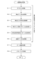
<<< §1. 本発明に係る情報保存装置の基本的実施形態 >>>
図1は、本発明に係る情報保存装置の基本的実施形態の構成を示すブロック図である。この実施形態に係る情報保存装置は、デジタルデータを情報記録媒体に書き込んで保存する機能を果たす装置であり、図示のとおり、保存処理用コンピュータ100、ビーム露光装置200、パターニング装置300によって構成される。
<<< §1. Basic embodiment of information storage apparatus according to the present invention >>
FIG. 1 is a block diagram showing a configuration of a basic embodiment of an information storage device according to the present invention. The information storage device according to this embodiment is a device that performs the function of writing and storing digital data on an information recording medium, and includes a storage processing computer 100, a
ここで、保存処理用コンピュータ100は、保存対象となるデジタルデータDに基づいて、描画データEを作成する処理を実行する。ビーム露光装置200は、この描画データEに基づいて、情報記録媒体となる基板S上に、電子線またはレーザ光を用いたビーム露光を行う装置であり、このビーム露光によって、基板S上には描画用パターンが形成される。パターニング装置300は、露光を受けた基板Sに対してパターニング処理を行うことにより、描画データEに応じた物理的構造パターンを形成し、情報記録媒体Mを作成する。結局、情報記録媒体Mには、デジタルデータDに応じた情報が物理的構造パターンとして記録される。
Here, the storage processing computer 100 executes a process of creating the drawing data E based on the digital data D to be stored. The
保存処理用コンピュータ100は、図示のとおり、データ入力部110、単位データ生成部120、単位ビット行列生成部130、単位ビット図形パターン生成部140、単位記録用図形パターン生成部150、描画データ生成部160を有している。以下、これら各部の機能について順に説明を行う。もっとも、これら各部は、実際には、コンピュータに専用のプログラムを組み込むことにより実現される構成要素であり、保存処理用コンピュータ100は、汎用のコンピュータに専用のプログラムをインストールすることにより構成することができる。
As shown in the figure, the storage processing computer 100 includes a
まず、データ入力部110は、保存対象となるデジタルデータDを入力する機能をもった構成要素であり、入力したデジタルデータDを一時的に格納する機能も備えている。保存対象となるデジタルデータDは、文書データ、画像データ、音声データなど、どのような形態のものであってもかまわない。
First, the
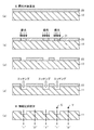
単位データ生成部120は、データ入力部110が入力したデジタルデータDを、所定のビット長単位で分割することにより、複数の単位データを生成する構成要素である。ここでは、説明の便宜上、図2の上段に示すように、デジタルデータDをビット長uの単位で分割することにより、4組の単位データが生成された場合を例にとって以下の説明を行うことにし、第i番目の単位データを符号Uiで示す(この例では、i=1〜4)。以下、本願において用いられる「単位」なる語句を冠した用語は、いずれも「1つの単位データ」について作成されたものであることを示す。
The unit
個々の単位データUiのビット長は、必ずしも等しくする必要はなく、互いに異なるビット長をもった複数の単位データを生成してもかまわない。ただ、実用上は、後述するビット記録領域Abを同一形状同一面積の領域とするのが好ましく、そのためには、予め共通のビット長uを定めておき、すべての単位データUiが同じビット長uをもつデータになるようにするのが好ましい。 The bit lengths of the individual unit data Ui are not necessarily equal, and a plurality of unit data having different bit lengths may be generated. However, for practical use, it is preferable that a bit recording area Ab described later is an area having the same shape and the same area. For this purpose, a common bit length u is determined in advance, and all unit data Ui have the same bit length u. It is preferable that the data has
共通のビット長uは、任意の値に設定することができるが、実用上は、m行n列の単位ビット行列を構成することができるように、u=m×nに設定し、単位データ生成部120が、デジタルデータを(m×n)ビットからなる単位データに分割するようにすればよい。ここでは説明の便宜上、m=n=5に設定して、5行5列の単位ビット行列を構成することができるように、u=25ビットに設定した例を示す(実用上は、uの値はより大きな値に設定するのが好ましい。)。図2に示す第1番目の単位データU1は、このような設定に基づいて生成された単位データであり、25ビットのデータから構成されている。
The common bit length u can be set to an arbitrary value. However, in practice, u = m × n is set so that a unit bit matrix of m rows and n columns can be formed. The
単位データ生成部120は、たとえば、入力したデジタルデータDを先頭からuビットずつに区切って分割してゆき、それぞれを単位データU1,U2,U3,... とすればよい。この場合、デジタルデータD全体の長さがビット長uの整数倍になっていないと、最後の単位データの長さがビット長uに満たなくなる。そこで、すべての単位データの長さを共通のビット長uに揃えたい場合には、デジタルデータDの末尾にダミービットを追加して、全体の長さがビット長uの整数倍になるように調整すればよい。
For example, the unit
なお、デジタルデータDの分割方法は、必ずしも先頭から所定のビット長uごとに区切ってゆく方法に限定されるものではなく、たとえば、4分割する場合、第1,5,9,... 番目のビットを抽出したものを第1の単位データU1とし、第2,6,10,... 番目のビットを抽出したものを第2の単位データU2とし、第3,7,11,... 番目のビットを抽出したものを第3の単位データU3とし、第4,8,12,... 番目のビットを抽出したものを第4の単位データU4とする、というような分割方法を採ることも可能である。 Note that the method of dividing the digital data D is not necessarily limited to a method of dividing the digital data D by a predetermined bit length u from the beginning. For example, when dividing into four, the first, fifth, ninth,. Are extracted as the first unit data U1, the extracted second, sixth, tenth,... Bits as the second unit data U2, and the third, seventh,. A division method such that the third unit data U3 is obtained by extracting the th bit, and the fourth unit data U4 is obtained by extracting the fourth, eighth, twelfth,... Bits. It is also possible to take.
単位データ生成部120によって生成された個々の単位データUiは、単位ビット行列生成部130に与えられる。単位ビット行列生成部130は、個々の単位データUiを構成するデータビットをm行n列の二次元行列状に配置することにより、単位ビット行列B(Ui)を生成する処理を行う。
The individual unit data Ui generated by the unit
図2には、第1番目の単位データU1を構成する25ビットのデータを先頭から5ビットずつに区切って、「11101」,「10110」,「01001」,「11001」,「10110」なる5グループを形成し、個々のグループを1行に配置した5行5列の行列からなる単位ビット行列B(U1)を生成した例が示されている。もちろん、単位データU2,U3,U4についても同様の方法により、単位ビット行列B(U2),B(U3),B(U4)が生成されることになる。 In FIG. 2, the 25-bit data constituting the first unit data U1 is divided into 5 bits from the beginning, and “11101”, “10110”, “010001”, “11001”, “10110” 5 An example is shown in which a unit bit matrix B (U1) consisting of a matrix of 5 rows and 5 columns in which groups are formed and individual groups are arranged in one row is shown. Of course, the unit bit matrices B (U2), B (U3), and B (U4) are generated for the unit data U2, U3, and U4 by the same method.
こうして単位ビット行列生成部130で生成された個々の単位ビット行列B(Ui)は、単位ビット図形パターン生成部140に与えられる。単位ビット図形パターン生成部140は、個々の単位ビット行列B(Ui)を、二次元平面上の所定のビット記録領域内に配置された幾何学的なパターンに変換することにより、単位ビット図形パターンP(Ui)を生成する処理を行う。
The individual unit bit matrix B (Ui) generated by the unit bit
図2の中段には、5行5列の行列からなる単位ビット行列B(U1)に基づいて作成された単位ビット図形パターンP(U1)の実例が示されている。この実例の場合、二次元平面上に正方形のビット記録領域Ab(図に破線で示す領域)が定義され、その中に黒く塗りつぶした小さな正方形状のドット(以下、ビット図形と呼ぶ)を配置することにより、単位ビット図形パターンP(U1)が形成されている。 The middle part of FIG. 2 shows an example of a unit bit figure pattern P (U1) created based on a unit bit matrix B (U1) consisting of a 5 × 5 matrix. In this example, a square bit recording area Ab (area shown by a broken line in the figure) is defined on a two-dimensional plane, and a small square dot (hereinafter referred to as a bit figure) painted black is placed therein. As a result, the unit bit figure pattern P (U1) is formed.
ここで、個々のビット図形は、単位ビット行列B(U1)を構成するビット”1”に対応している。別言すれば、ビット記録領域Ab内には、単位ビット行列B(U1)に対応して5行5列の行列が定義され、単位ビット行列B(U1)内のビット”1”に対応する位置にのみビット図形が配置され、ビット”0”に対応する位置には何も配されていない。したがって、この単位ビット図形パターンP(U1)は、5行5列の行列を構成する各位置におけるビット図形の有無によって、単位ビット行列B(U1)を構成する25ビットの情報を表現していることになる。 Here, each bit figure corresponds to the bit “1” constituting the unit bit matrix B (U1). In other words, a 5 × 5 matrix is defined in the bit recording area Ab corresponding to the unit bit matrix B (U1), and corresponds to the bit “1” in the unit bit matrix B (U1). A bit figure is arranged only at the position, and nothing is arranged at the position corresponding to the bit “0”. Therefore, this unit bit figure pattern P (U1) expresses 25-bit information constituting the unit bit matrix B (U1) by the presence or absence of the bit figure at each position constituting the 5 × 5 matrix. It will be.
もちろん、個々のビット図形を、単位ビット行列B(U1)を構成するビット”0”に対応させて配置するようにしてもかまわない。この場合は、単位ビット行列B(U1)内のビット”0”に対応する位置にのみビット図形が配置され、ビット”1”に対応する位置には何も配置されないことになる。要するに、単位ビット図形パターン生成部140は、単位ビット行列B(U1)を構成する個々のビット”1”および個々のビット”0”のうちのいずれか一方を、閉領域からなる個々のビット図形に変換する処理を行えばよい。なお、個々のビット図形を示すデータの形式は、任意の形式でかまわない。たとえば、1つのビット図形を矩形によって構成する場合であれば、単位ビット図形パターンP(U1)を示すデータとして、個々のビット図形の4頂点の座標値(対角2頂点の座標値でもよい)を示すデータを用いることもできるし、個々のビット図形の中心点(左下隅点等でもよい)の座標値を示すデータと共通の矩形形状を有するビット図形の縦横の辺の長さを示すデータとを用いることもできる。あるいは、円形のビット図形を採用する場合であれば、個々のビット図形の中心点の座標値を示すデータと共通の半径値を示すデータとを用いることもできる。
Of course, each bit figure may be arranged in correspondence with the bit “0” constituting the unit bit matrix B (U1). In this case, the bit figure is arranged only at the position corresponding to the bit “0” in the unit bit matrix B (U1), and nothing is arranged at the position corresponding to the bit “1”. In short, the unit bit figure
もちろん、単位データU2,U3,U4について生成された単位ビット行列B(U2),B(U3),B(U4)も、同様の方法で幾何学的なパターンに変換され、単位ビット図形パターンP(U2),P(U3),P(U4)が生成される。こうして生成された各単位ビット図形パターンP(U1)〜P(U4)を何らかの方法で媒体上に形成すれば、デジタルデータDの情報を媒体に記録することができる。ただ、本発明では、後に行われる読出処理の便宜を考慮して、各単位ビット図形パターンP(U1)〜P(U4)にそれぞれ位置合わせマークを付加することにする。 Of course, the unit bit matrices B (U2), B (U3), and B (U4) generated for the unit data U2, U3, and U4 are also converted into a geometric pattern by the same method, and the unit bit figure pattern P (U2), P (U3), and P (U4) are generated. If the unit bit figure patterns P (U1) to P (U4) generated in this way are formed on the medium by some method, the information of the digital data D can be recorded on the medium. However, in the present invention, an alignment mark is added to each of the unit bit figure patterns P (U1) to P (U4) in consideration of the convenience of the reading process performed later.
単位記録用図形パターン生成部150は、この位置合わせマークの付加を行う構成要素であり、本願では、この位置合わせマークが付加された状態の単位ビット図形パターンP(Ui)を、単位記録用図形パターンR(Ui)と呼んでいる。結局、単位記録用図形パターン生成部150は、単位ビット図形パターン生成部140が生成した単位ビット図形パターンP(Ui)に位置合わせマークを付加し、単位記録用図形パターンR(Ui)を生成する処理を行うことになる。
The unit recording graphic pattern generation unit 150 is a component that adds the alignment mark. In the present application, the unit bit graphic pattern P (Ui) with the alignment mark added is used as the unit recording graphic. This is called pattern R (Ui). Eventually, the unit recording graphic pattern generation unit 150 adds an alignment mark to the unit bit graphic pattern P (Ui) generated by the unit bit graphic
図2の中段には、単位ビット図形パターンP(U1)の外側4隅に十字状の位置合わせマークQを付加し、単位記録用図形パターンR(U1)を生成した例が示されている。ここでは、単位ビット図形パターンP(U1)が形成されたビット記録領域Ab(破線の正方形)と、その外側4隅に配置された位置合わせマークQとを包含する領域を、単位記録領域Au(一点鎖線の正方形)と呼ぶことにする。単位記録用図形パターンR(U1)は、この単位記録領域Au内に形成された図形パターンということになる。 The middle part of FIG. 2 shows an example in which a unit recording graphic pattern R (U1) is generated by adding cross-shaped alignment marks Q to the outer four corners of the unit bit graphic pattern P (U1). Here, an area including the bit recording area Ab (dashed square) in which the unit bit figure pattern P (U1) is formed and the alignment marks Q arranged at the four outer corners is defined as a unit recording area Au ( It will be called a one-dot chain line square). The unit recording graphic pattern R (U1) is a graphic pattern formed in the unit recording area Au.
位置合わせマークQは、§3で述べる読出処理において、個々のビット記録領域Abを認識するために利用される。そのため、位置合わせマークQは、ビット記録領域Abに対して特定の位置(図示の例では、ビット記録領域Abの外側4隅の位置)に配置される。図示の例では、十文字状の位置合わせマークQを用いた例が示されているが、個々のビットを表すビット図形(図示の例の場合、黒く塗りつぶした小さな正方形)と区別することができる図形であれば、どのような形状の図形を用いてもかまわない。 The alignment mark Q is used for recognizing individual bit recording areas Ab in the reading process described in §3. Therefore, the alignment mark Q is arranged at a specific position with respect to the bit recording area Ab (in the illustrated example, positions at the four outer corners of the bit recording area Ab). In the example shown in the figure, an example using a cross-shaped alignment mark Q is shown, but a figure that can be distinguished from a bit figure representing each bit (in the example shown, a small black square). Any shape can be used as long as it is.
また、図示の例では、ビット記録領域Abの外側に位置合わせマークQを配置しているが、ビット記録領域Abの内側に位置合わせマークQを配置することも可能である。ただ、ビット記録領域Abの内側に配置する場合は、個々のビットを表すビット図形と干渉するおそれがあるため、実用上は、図示の例のように、ビット記録領域Abの外側に位置合わせマークQを配置するのが好ましい。この位置合わせマークQの形状や配置のバリエーションについては、§4で改めて述べることにする。 In the illustrated example, the alignment mark Q is arranged outside the bit recording area Ab. However, the alignment mark Q can be arranged inside the bit recording area Ab. However, in the case of being arranged inside the bit recording area Ab, there is a possibility of interference with bit figures representing individual bits. Therefore, in practice, an alignment mark is placed outside the bit recording area Ab as shown in the example in the figure. Q is preferably arranged. Variations in the shape and arrangement of the alignment mark Q will be described again in §4.
こうして、単位記録用図形パターン生成部150が、4組の単位記録用図形パターンR(U1)〜R(U4)を生成したら、描画データ生成部160が、これらを描画するための描画データEを生成する処理を行う。具体的には、描画データ生成部160は、図2の下段に示されているように、4組の単位記録領域R(U1)〜R(U4)を二次元行列状に配置することにより(この例の場合は2行2列)、4組の単位記録用図形パターンR(U1)〜R(U4)をすべて含んだ描画用パターンP(E)を生成し、当該描画用パターンP(E)を描画するための描画データEを生成する処理を行う。
Thus, when the unit recording graphic pattern generation unit 150 generates four sets of unit recording graphic patterns R (U1) to R (U4), the drawing
以上、図1に示す保存処理用コンピュータ100の個々の構成要素の処理機能を述べた。こうして生成された描画データEは、ビーム露光装置200に与えられる。ビーム露光装置200は、描画データEに基づいて、露光対象基板S上にビーム露光を行う装置であり、種々の電子デバイスの製造プロセスに利用される半導体フォトリソグラフィ用の電子線描画装置やレーザ描画装置を利用して構成することができる。ビーム露光装置200として電子線描画装置を用いた場合は、露光対象基板Sの表面上に電子線によって描画用パターンP(E)が描かれ、ビーム露光装置200としてレーザ描画装置を用いた場合は、露光対象基板Sの表面上にレーザビームによって描画用パターンP(E)が描かれる。
The processing functions of the individual components of the storage processing computer 100 shown in FIG. 1 have been described above. The drawing data E generated in this way is given to the
なお、図2には、説明の便宜上、ビット記録領域Abの輪郭線を破線で示し、単位記録領域Auの輪郭線を一点鎖線で示してあるが、これらの線は、描画用パターンP(E)の構成要素ではない。実際に露光対象基板S上に描かれる図形パターンは、個々のビットを表すビット図形(図示の例の場合、黒く塗りつぶした小さな正方形)と十文字状の位置合わせマークQである。 In FIG. 2, for convenience of description, the outline of the bit recording area Ab is indicated by a broken line, and the outline of the unit recording area Au is indicated by a one-dot chain line. ) Is not a component. The graphic pattern actually drawn on the exposure target substrate S is a bit graphic representing each bit (in the example shown, a small black square) and a cross-shaped alignment mark Q.
このように、描画データEは、ビーム露光装置200に与えて、露光対象基板S上に描画用パターンP(E)を描画させるために用いられるデータであるため、そのデータフォーマットは、用いるビーム露光装置200に依存したものにする必要がある。現在、一般的なLSI設計に用いられている電子線描画装置やレーザ描画装置を用いて任意の図形パターンを描画させる場合、当該図形パターンの輪郭線を示すベクトル形式の描画データが用いられている。したがって、実用上、描画データ生成部160は、個々のビット図形や位置合わせマークの輪郭線を示す描画データEを生成すればよい。
Thus, since the drawing data E is data used to give the drawing pattern P (E) on the exposure target substrate S by giving it to the
図3は、図2に示す単位記録用図形パターンR(U1)の拡大図である。図2では、ビット”1”を示すビット図形として、黒く塗りつぶした小さな正方形の例を示したが、図3に示す例では、個々のビット図形Fは、正方形の輪郭線を示すベクトルデータとして表現される。同様に、4隅に配置された位置合わせマークQ1〜Q4は、十文字状の輪郭線を示すベクトルデータとして表現される。ビーム露光装置200は、個々のビット図形Fや位置合わせマークQ1〜Q4の輪郭線を示す描画データEに基づいて、当該輪郭線の内側部分に対してビーム露光を行う処理を行う。したがって、露光対象基板S上には、図2に示すように、黒く塗りつぶされた正方形や十文字状の図形パターンが形成されることになる。
FIG. 3 is an enlarged view of the unit recording graphic pattern R (U1) shown in FIG. In FIG. 2, an example of a small square filled with black is shown as a bit figure indicating the bit “1”. However, in the example shown in FIG. 3, each bit figure F is expressed as vector data indicating a square outline. Is done. Similarly, the alignment marks Q1 to Q4 arranged at the four corners are expressed as vector data indicating a cross-shaped outline. The
図3には、等間隔で配置された横方向格子線X1〜X7と、等間隔で配置された縦方向格子線Y1〜Y7とが描かれている。これらの各格子線は、個々のビット図形Fや位置合わせマークQ1〜Q4の配置位置を決定する役割を果たす。すなわち、横方向格子線X1〜X7と縦方向格子線Y1〜Y7との各交点を格子点Lと呼ぶことにすると、個々のビット図形Fや位置合わせマークQ1〜Q4は、その中心がいずれかの格子点Lの位置にくるように配置されている。 In FIG. 3, horizontal grid lines X1 to X7 arranged at equal intervals and vertical grid lines Y1 to Y7 arranged at equal intervals are drawn. Each of these grid lines plays a role of determining the arrangement positions of the individual bit figures F and the alignment marks Q1 to Q4. That is, if each intersection of the horizontal grid lines X1 to X7 and the vertical grid lines Y1 to Y7 is referred to as a grid point L, each bit figure F and the alignment marks Q1 to Q4 have any center. It arrange | positions so that it may come to the position of the lattice point L of.
たとえば、位置合わせマークQ1は、格子線X1,Y1が交わる格子点上に配置され、位置合わせマークQ2は、格子線X1,Y7が交わる格子点上に配置され、位置合わせマークQ3は、格子線X7,Y1が交わる格子点上に配置され、位置合わせマークQ4は、格子線X7,Y7が交わる格子点上に配置されている。 For example, the alignment mark Q1 is disposed on the lattice point where the lattice lines X1 and Y1 intersect, the alignment mark Q2 is disposed on the lattice point where the lattice lines X1 and Y7 intersect, and the alignment mark Q3 is disposed on the lattice line. The alignment mark Q4 is disposed on the lattice point where the lattice lines X7 and Y7 intersect, and the alignment mark Q4 is disposed on the lattice point where X7 and Y1 intersect.
また、5本の横方向格子線X2〜X6と5本の縦方向格子線Y2〜Y6とがそれぞれ交わる25個の格子点は、図2の中段に示す5行5列の単位ビット行列B(U1)に対応し、この単位ビット行列B(U1)におけるビット”1”に対応する格子点位置に、ビット図形Fが配置されている(前述したとおり、ビット”0”に対応する格子点位置に、ビット図形Fを配置してもかまわない)。 25 lattice points at which the five horizontal lattice lines X2 to X6 and the five vertical lattice lines Y2 to Y6 intersect each other are the unit bit matrix B (5 × 5) shown in the middle of FIG. U1), the bit figure F is arranged at the grid point position corresponding to the bit “1” in the unit bit matrix B (U1) (as described above, the grid point position corresponding to the bit “0”). In addition, the bit figure F may be arranged).
一般論として説明すれば、単位ビット図形パターン生成部140は、m行n列からなる単位ビット行列B(Ui)を構成する個々のビットを、m行n列の行列状に配置された格子点Lに対応づけ、ビット”1”またはビット”0”に対応する格子点L上に所定形状のビット図形Fを配置することにより単位ビット図形パターンP(Ui)を生成する処理を行えばよい。
Explaining in general terms, the unit bit figure
もちろん、実際の描画データEに含まれる図形、すなわち、描画用パターンP(E)に含まれる図形は、個々のビット図形Fと個々の位置合わせマークQ1〜Q4のみであり、図示されている各格子線X1〜X7,Y1〜Y7、ビット記録領域Abの輪郭線(破線)、単位記録領域Auの輪郭線(一点鎖線)は、実際には描画されない。 Of course, the figure included in the actual drawing data E, that is, the figure included in the drawing pattern P (E) is only the individual bit figure F and the individual alignment marks Q1 to Q4. The lattice lines X1 to X7, Y1 to Y7, the contour line (broken line) of the bit recording area Ab, and the contour line (one-dot chain line) of the unit recording area Au are not actually drawn.
なお、描画データEには、露光対象基板S上に描画される描画用パターンP(E)の実寸を示す情報も含まれることになるが、この実寸は、用いるビーム露光装置200の描画精度を考慮して設定すればよい。
The drawing data E includes information indicating the actual size of the drawing pattern P (E) to be drawn on the exposure target substrate S. This actual size indicates the drawing accuracy of the
現在、一般的なLSI設計に用いられている高精度の電子線描画装置を用いたパターニング処理では、基板S上に40nm程度のサイズをもった図形を安定的に形成することができる。したがって、このような電子線描画装置をビーム露光装置200として用いれば、図示の格子線間隔(格子点Lのピッチ)を100nm程度に設定することが可能になり、一辺が50nm程度のビット図形Fを形成することが十分に可能である。このように微細な図形パターンを描画する場合、実際には、ビット図形Fは正確な正方形にはならず、位置合わせマークQ1〜Q4は正確な十文字にはならないが、実用上の支障は生じない。
Currently, a pattern having a size of about 40 nm can be stably formed on the substrate S by patterning using a high-precision electron beam drawing apparatus used in general LSI design. Therefore, when such an electron beam drawing apparatus is used as the
そもそもビット図形Fは、格子点Lの位置に図形が有るか無いかの二値状態を判定する役割を果たせば足りるので、その形状は矩形でも、円でも、任意形状でもかまわない。また、位置合わせマークQ1〜Q4は、ビット記録領域Abの位置を示す役割を果たせば足りるので、その形状は、ビット図形Fと区別可能であれば、どのような形状であってもかまわない。したがって、40nm程度のサイズをもった図形を安定的に形成可能な性能をもった電子線描画装置を利用すれば、上述したように、縦横100nm程度のピッチでビット図形Fを配置することが可能であり、高い集積度をもった情報記録が可能になる。 In the first place, the bit figure F only needs to play the role of determining the binary state of whether or not a figure is present at the position of the lattice point L, so the shape may be a rectangle, a circle, or an arbitrary shape. Further, since the alignment marks Q1 to Q4 need only serve to indicate the position of the bit recording area Ab, the shape may be any shape as long as it can be distinguished from the bit graphic F. Therefore, if an electron beam drawing apparatus having a performance capable of stably forming a figure having a size of about 40 nm is used, the bit figure F can be arranged at a pitch of about 100 nm vertically and horizontally as described above. Thus, information recording with a high degree of integration becomes possible.
一方、レーザ描画装置をビーム露光装置200として用いる場合、レーザビームのスポット径は使用するレーザ光の波長に依存し、その最小値は波長と同程度になる。たとえば、ArFエキシマレーザを用いた場合、スポット径は200nm程度であるため、電子線描画装置を利用した場合に比べれば、情報記録の集積度は若干低下するが、それでも、一般的な光学的記録媒体と同程度の集積度をもった情報記録が可能である。
On the other hand, when a laser drawing apparatus is used as the
図3に示す例の場合、単位ビット図形パターンP(U1)は、矩形状(正方形状)のビット記録領域Ab内に配置されたパターンになっており、これに位置合わせマークQ1〜Q4を付加することにより構成される単位記録用図形パターンR(U1)も、矩形状(正方形状)の単位記録領域Au内に配置されたパターンになっている。本発明を実施するにあたって、ビット記録領域Abや単位記録領域Auは、必ずしも矩形状の領域にする必要はないが、図2の下段に示すように、複数の単位記録用図形パターンR(U1)〜R(U4)を並べて描画用パターンP(E)を生成することを考慮すると、ビット記録領域Abおよび単位記録領域Auを、いずれも矩形状の領域にしておくのが効率的である。 In the case of the example shown in FIG. 3, the unit bit figure pattern P (U1) is a pattern arranged in a rectangular (square) bit recording area Ab, and alignment marks Q1 to Q4 are added thereto. The unit recording figure pattern R (U1) formed by doing so is also a pattern arranged in a rectangular (square) unit recording area Au. In carrying out the present invention, the bit recording area Ab and the unit recording area Au do not necessarily have to be rectangular areas. However, as shown in the lower part of FIG. 2, a plurality of unit recording graphic patterns R (U1) Considering that the drawing pattern P (E) is generated by arranging ~ R (U4), it is efficient to set both the bit recording area Ab and the unit recording area Au to rectangular areas.
したがって、実用上は、単位ビット図形パターン生成部140が、矩形状のビット記録領域Ab内に配置された単位ビット図形パターンP(Ui)を生成し、単位記録用図形パターン生成部150が、この矩形状のビット記録領域Abの外部に位置合わせマークQ1〜Q4を付加することにより、ビット記録領域Abおよび位置合わせマークQ1〜Q4を包含する矩形状の単位記録領域Au内に配置された単位記録用図形パターンR(Ui)を生成するようにするのが好ましい。そうすれば、描画データ生成部160は、これら矩形状の単位記録領域Auを二次元行列状に配置することにより、複数の単位記録用図形パターンR(U1)〜R(U4)を含んだ描画用パターンP(E)を生成し、当該描画用パターンP(E)を描画するための描画データEを生成することができる。
Therefore, practically, the unit bit graphic
単位記録領域Auのサイズは、任意に設定してかまわない。たとえば、図3に示す例の場合、一辺が50μmの正方形からなる単位記録領域Auを定義し、縦横100nm程度のピッチでビット図形Fを配置するようにすれば、1つの単位記録領域Au内に約30KBの情報を記録することができる。そこで、たとえば、一辺が150mm程度の正方形状の基板を情報記録媒体として用い、この基板上に、一辺が50μmの正方形からなる単位記録領域Auを二次元行列上に配置すれば、当該情報記録媒体1枚に270GBものデータを記録することができる。 The size of the unit recording area Au may be set arbitrarily. For example, in the example shown in FIG. 3, if a unit recording area Au consisting of a square with a side of 50 μm is defined and bit figures F are arranged at a pitch of about 100 nm in length and width, one unit recording area Au is included. About 30 KB of information can be recorded. Therefore, for example, if a square substrate having a side of about 150 mm is used as an information recording medium, and unit recording areas Au each consisting of a square having a side of 50 μm are arranged on the two-dimensional matrix, the information recording medium Data of as much as 270 GB can be recorded on one sheet.
<<< §2. 媒体上における物理的構造パターンの形成 >>>
ここでは、図1に示すビーム露光装置200による露光プロセスと、パターニング装置300によるパターニングプロセスとを、より詳細に説明する。§1で述べたとおり、ビーム露光装置200は、描画データEに基づいて、情報記録媒体となる基板S上に、電子線またはレーザ光を用いたビーム露光を行う装置であり、パターニング装置300は、露光を受けた基板Sに対してパターニング処理を行うことにより、描画データEに応じた物理的構造パターン(描画用パターンP(E))が形成された情報記録媒体を生成する装置である。
<<< §2. Formation of physical structure pattern on medium >>
Here, the exposure process by the
これらの装置は、実際には、LSIの製造プロセスで利用されている半導体リソグラフィ用の装置をそのまま転用することができる。別言すれば、ビーム露光装置200によるビーム露光プロセスや、パターニング装置300によるパターニングプロセスは、従来の一般的なLSIの製造プロセスをそのまま利用して実施することが可能である。ただ、LSIを製造する場合に用いる描画データは、たとえば、チャネル領域、ゲート領域、ソース領域、ドレイン領域、配線領域など、半導体素子の各領域を構成するための図形パターンを示すデータであるのに対して、本発明で用いられる描画データEは、データビット”1”もしくは”0”を示すビット図形Fと、読み出し時に用いる位置合わせマークQを構成するための図形パターンを示すデータということになる。
In practice, these apparatuses can be used as they are for semiconductor lithography used in the LSI manufacturing process. In other words, the beam exposure process by the
図4は、図1に示すビーム露光装置200による露光工程およびパターニング装置300によるパターニング工程の具体例を示す側断面図である(切断面のみを示し、奥の構造の図示は省略する)。まず、図4(a) に示すような露光対象基板Sを用意する。この例の場合、露光対象基板Sは、被成形層10とレジスト層20によって構成されている。なお、ここでは一層からなるレジスト層20を用いた例を示すが、後述するパターニング工程において必要となる場合には、二層以上からなるレジスト層を用いるようにしてもかまわない。また、レジストのような有機膜だけでなく、金属膜のような無機膜(エッチングストッパとして機能するいわゆるハードマスク)を併せて用いるようにしてもよい。
FIG. 4 is a side sectional view showing a specific example of the exposure process by the
ここで、被成形層10は、パターニング工程において成形対象となる層であり、最終的には、デジタルデータが記録された情報記録媒体Mとなる部分である。既に述べたとおり、本発明の目的は、長期的な耐久性を維持する情報記録を可能とする点にあるので、被成形層10には、このような目的達成に適した材料からなる基板を利用すればよい。具体的には、透明な材料としては、ガラス基板、特に石英ガラス基板を被成形層10として用いるのが最適である。もちろん、シリコン基板のような不透明な材料を被成形層10として用いることも可能である。石英ガラス基板やシリコン基板といった無機材料は、物理的な損傷を受けにくく、化学的な汚染も受けにくい材質であり、本発明における情報記録媒体に利用するのに最適な材料である。
Here, the layer to be molded 10 is a layer to be molded in the patterning step, and is finally a portion that becomes an information recording medium M on which digital data is recorded. As described above, the object of the present invention is to enable information recording to maintain long-term durability. Therefore, a substrate made of a material suitable for achieving such an object is formed on the
一方、レジスト層20としては、被成形層10に対するパターニングを行うのに適した材料を用いればよい。すなわち、電子線もしくはレーザビームの露光によって組成が変化し、かつ、被成形層10に対するエッチング工程において保護膜として機能する性質を有する材料を用いればよい。もちろん、現像時に露光部が溶解する性質をもったポジ型レジストを用いてもよいし、現像時に非露光部が溶解する性質をもったネガ型レジストを用いてもよい。
On the other hand, as the resist
なお、露光対象基板Sの形状や大きさは任意でかまわない。現在、フォトマスクとして一般に用いられている石英ガラス基板は、152×152×6.35mmといった標準規格の矩形状の基板が用いられることが多い。また、シリコン基板としては、直径6インチ,8インチ,12インチなどの規格に応じた厚み1mm程度の円盤状ウエハが用いられることが多い。露光対象基板Sとしては、これらの標準的な基板を被成形層10として、その上面にレジスト層20を形成したものを用いればよい。
The shape and size of the exposure target substrate S may be arbitrary. At present, a quartz glass substrate that is generally used as a photomask is often a standard rectangular substrate of 152 × 152 × 6.35 mm. Further, as the silicon substrate, a disk-shaped wafer having a thickness of about 1 mm in accordance with a standard such as a diameter of 6 inches, 8 inches, or 12 inches is often used. As the exposure target substrate S, a substrate in which these standard substrates are formed
以下、説明の便宜上、被成形層10として石英ガラス基板を用い、レジスト層20としてポジ型レジストを用いた実施例を述べることにする。したがって、図4(a) に示す露光対象基板Sは、石英ガラス基板10上にポジ型レジスト層20を形成した基板ということになる。もちろん、本発明はこのような実施例に限定されるものではない。
Hereinafter, for convenience of explanation, an example in which a quartz glass substrate is used as the
結局、図1に示すビーム露光装置200は、被成形層10とこれを覆うレジスト層20とを有する露光対象基板Sに対して、レジスト層20の表面にビーム露光を行うことになる。図4(b) は、ビーム露光装置200による露光プロセスを示している。§1で述べたとおり、ビーム露光装置200による露光は、ビット図形Fの内部および位置合わせマークQの内部に対してのみ行われる。したがって、レジスト層20は、露光プロセスを経ることにより、露光部21と非露光部22とに分けられる。ここで、非露光部22の化学的組成は元のままであるが、露光部21の化学的組成は変化する。
As a result, the
パターニング装置300は、このような露光プロセスが完了した後の基板Sに対してパターニングを行う装置であり、図1に示すとおり、現像処理部310とエッチング処理部320とを有している。
The
現像処理部310は、レジスト層の露光部21(ポジ型レジストを用いた場合)または非露光部22(ネガ型レジストを用いた場合)を溶解する性質をもった現像液に、露光後の基板Sを含浸させてその一部を残存部とする現像処理を行う。図4(c) は、図4(b) に示す基板Sに対して、このような現像処理を施した状態を示している。ここに示す実施例では、ポジ型レジストが用いられているため、現像処理によって露光部21が現像液に溶解し、非露光部22が残存部23として残ることになる。
The
一方、エッチング処理部320は、現像後の基板Sに対してエッチング処理を行う。図4(c) に示す実施例の場合、残存部23をマスクとして被成形層10に対するエッチング処理が行われることになる。具体的には、図4(c) に示す基板Sを、被成形層10に対する腐食性が、レジスト層の残存部23に対する腐食性よりも強いエッチング液に含浸させればよい(もちろん、ドライエッチングなど、エッチング液に含浸させない方法を採用してもかまわない)。
On the other hand, the
図4(d) は、エッチング処理部320によるエッチング処理が行われた状態を示している。被成形層10の上面のうち、マスクとなる残存部23に覆われている部分は腐食を受けないが、露出している部分は腐食を受け、凹部が形成される。こうして、被成形層10は、上面に凹凸構造が形成された被成形層11に加工されることになる。エッチング処理部320は、この後、レジスト層の残存部23を剥離除去し、被成形層11を洗浄乾燥する処理機能を有している。
FIG. 4D shows a state where the etching processing by the
このようなプロセスを経て、最終的に図4(e) に示すような加工後の被成形層11が得られる。こうして得られた被成形層11が、本発明に係る情報保存装置によってデジタルデータが書き込まれた情報記録媒体Mに他ならない。図示のとおり、この情報記録媒体Mの上面には物理的な凹凸構造が形成されており、凹部Cと凸部Vとによって、ビット”1”およびビット”0”が表現されている。したがって、図に太い一点鎖線で示す位置(図3に示す格子点Lに対応する位置)について、媒体表面が凹部Cを構成しているか、凸部Vを構成しているかを検出することにより、ビット”1”およびビット”0”の読み出しが可能になる。
Through such a process, the processed
もちろん、図示の例とは逆に、凹部Cをビット”0”とし、凸部Vをビット”1”とする記録方式を採ることも可能である。いずれをビット”0”とし、いずれをビット”1”とするかは、これまで述べてきたプロセスに応じて定まる事項である。たとえば、§1で述べた例の場合、単位ビット図形パターン生成部140において、単位ビット行列のビット”1”に対応する格子点Lの位置にビット図形Fを配置しているが、逆に、ビット”0”に対応する格子点Lの位置にビット図形Fを配置するようにすれば、凹部と凸部のビット情報は逆転することになる。また、レジスト層20として、ポジ型レジストではなくネガ型レジストを用いた場合も、凹部と凸部の関係は逆転する。
Of course, contrary to the illustrated example, it is also possible to adopt a recording method in which the concave portion C is set to the bit “0” and the convex portion V is set to the bit “1”. Which is set to bit “0” and which is set to bit “1” is a matter determined according to the processes described so far. For example, in the case of the example described in §1, the unit bit graphic
こうして作成された情報記録媒体Mは、長期的な耐久性をもち、高い集積度をもって情報記録が行われており、しかも普遍的な方法で情報を読み出せる、という特徴を有している。 The information recording medium M created in this manner has long-term durability, information recording is performed with a high degree of integration, and information can be read out by a universal method.
すなわち、被成形層10として、石英ガラス基板やシリコン基板のような材料を用いれば、従来の紙、フィルム、レコード盤などの情報記録媒体に比べて、経年変化による劣化や、水や熱の作用による損傷を受けにくく、古代の石盤などと同様に数百年といった半永久的な時間的尺度での耐久性が得られる。もちろん、コンピュータ用のデータ記録媒体として一般に利用されている磁気記録媒体、光学式記録媒体、半導体記録媒体などと比較しても、格段に長い期間にわたって耐久性が得られる。したがって、本発明は、たとえば、半永久的に情報を記録しておくことが望ましい公文書などの情報保存に利用するのに最適である。 That is, when a material such as a quartz glass substrate or a silicon substrate is used as the layer to be molded 10, deterioration due to secular change and the action of water and heat, compared to conventional information recording media such as paper, film, and record board, etc. It is less likely to be damaged by, and can be durable on a semi-permanent time scale of hundreds of years, just like ancient stones. Needless to say, the durability can be obtained over a much longer period of time as compared with a magnetic recording medium, an optical recording medium, a semiconductor recording medium or the like generally used as a data recording medium for computers. Therefore, the present invention is most suitable for use in storing information such as an official document in which it is desirable to record information semipermanently.
また、§1で述べたとおり、ビーム露光装置200は、電子線またはレーザ光によって、微細な露光を行うことが可能なため、きわめて高い集積度をもって情報記録を行うことが可能である。たとえば、高精細な電子線描画装置を用いれば、ビット図形Fを100nm程度のピッチで書き込むことが可能であり、上述した標準的なサイズのフォトマスクやシリコン基板に、100GB〜1TB程度の容量をもった情報を保存することが可能になる。
Further, as described in
更に、本発明に係る情報記録媒体では、ビットの二値情報が、凹凸等の物理的構造として直接記録されるため、普遍的な方法で情報を読み出せるという特徴をもっている。すなわち、前掲の特許文献1および2には、円柱上の石英ガラスを媒体として、その内部に三次元的に情報を記録する技術が開示されているが、媒体内に三次元的に記録された情報を読み出すためには、コンピュータトモグラフィ等を利用した専用の読出装置が必要になり、フーリエ変換処理などの特殊な演算処理が必要になる。したがって、たとえば、数百年後に円柱状の記録媒体が無傷のまま残っていたとしても、専用の読出装置の技術が継承されていなければ、情報を読み出すことはできない。
Furthermore, the information recording medium according to the present invention is characterized in that the binary information of the bits is directly recorded as a physical structure such as unevenness, so that the information can be read out by a universal method. That is, the above-mentioned
これに対して、本発明に係る情報保存装置で作成された情報記録媒体には、ビットの二値情報が物理的構造として直接記録されているので、記録面を何らかの方法で拡大して画像として認識することができれば、少なくともビットの情報自体は読み出すことが可能である。別言すれば、本発明に係る情報記録媒体それ自体は三次元の構造体であるが、ビット情報の記録はあくまでも二次元的に行われているため、本発明に係る情報記録媒体が、仮に、数百年後あるいは数千年後に発掘された場合でも、普遍的な方法によってビット情報を読み出すことが可能になる。 On the other hand, since the binary information of bits is directly recorded as a physical structure on the information recording medium created by the information storage device according to the present invention, the recording surface is enlarged by some method as an image. If it can be recognized, at least the bit information itself can be read. In other words, the information recording medium according to the present invention itself is a three-dimensional structure, but since bit information is recorded two-dimensionally, the information recording medium according to the present invention is temporarily Even when excavated after hundreds of years or thousands of years, bit information can be read out by a universal method.
以上、本発明に係る情報保存装置によって、石英ガラス基板やシリコン基板の表面に、ビット”1”およびビット”0”のいずれか一方を示す凹部と他方を示す凸部とからなる凹凸構造を有する物理的構造パターンを形成する例を述べた。ただ、本発明を実施するにあたって、ビット情報を示す物理的構造は、必ずしも凹凸構造に限定されるものではない。そこで、図5の側断面図(切断面のみを示し、奥の構造の図示は省略する)を参照しながら、媒体上に物理的構造を形成する手法のバリエーションをいくつか述べておく、 As described above, the information storage device according to the present invention has a concavo-convex structure on the surface of a quartz glass substrate or silicon substrate, which includes a concave portion indicating one of the bits “1” and “0” and a convex portion indicating the other. An example of forming a physical structure pattern has been described. However, in carrying out the present invention, the physical structure indicating the bit information is not necessarily limited to the uneven structure. Therefore, several variations of the method of forming a physical structure on the medium will be described with reference to the side cross-sectional view of FIG. 5 (only the cut surface is shown, and the illustration of the back structure is omitted).
図5(a) は、パターニング装置300によって、ビット”1”およびビット”0”のいずれか一方を示す貫通孔Hと他方を示す非孔部Nとからなる網状構造を有する物理的構造パターンを形成した例を示す側断面図である。図示の網状構造体12では、太い一点鎖線で示す位置が図3に示す格子点Lに対応する位置であり、当該位置が貫通孔Hになっているか、非孔部N(貫通孔が形成されていない部分)になっているか、によって、図示のとおりビット”1”およびビット”0”が表現されている。
FIG. 5A shows a physical structure pattern having a network structure composed of a through hole H indicating one of the bits “1” and a bit “0” and a non-hole portion N indicating the other by the
このように、図5(a) に示す情報記録媒体の場合、凹凸構造ではなく、貫通孔の有無によってビットが表現されているため、媒体自体は網状構造体を構成することになるが、格子点Lの位置にビット情報を記録するという根本原理は、図4(e) に示す基本的な実施例と全く同様である。もちろん、貫通孔Hによりビット”0”を表現し、非孔部Nによりビット”1”を表現してもかまわない。図5(a) に示す網状構造体12を情報記録媒体Mとする場合は、エッチング処理部320によるエッチング工程(図4(d) )において、被成形層10の下面に達するまでエッチング処理を続けて貫通孔Hを形成すればよい。
Thus, in the case of the information recording medium shown in FIG. 5 (a), since the bits are expressed not by the concavo-convex structure but by the presence or absence of the through holes, the medium itself constitutes a network structure. The basic principle of recording bit information at the position of the point L is exactly the same as the basic embodiment shown in FIG. Of course, the bit “0” may be expressed by the through hole H, and the bit “1” may be expressed by the non-hole portion N. When the
一方、図5(b) 〜(d) は、図4(e) に示す情報記録媒体Mの凹部Cもしくは凸部Vまたはその双方の表面に付加層を形成した変形例を示す側断面図である。図5(b) に示す変形例の場合、凹部Cと凸部Vの双方の表面に付加層31が形成されており、図5(c) に示す変形例の場合、凸部Vの表面にのみ付加層32が形成されており、図5(d) に示す変形例の場合、凹部Cの表面にのみ付加層33が形成されている。
On the other hand, FIGS. 5B to 5D are side cross-sectional views showing modifications in which additional layers are formed on the surface of the concave portion C or the convex portion V of the information recording medium M shown in FIG. is there. In the case of the modification shown in FIG. 5 (b), the
付加層31,32,33としては、光反射性の材料(たとえば、アルミニウム、ニッケル、チタン、銀、クロム、シリコン、モリブデン、白金などの金属、これらの金属の合金、酸化物、窒化物など)もしくは光吸収性の材料(たとえば、金属の酸化物や窒化物といった化合物からなる材料、クロムを例にとれば、酸化クロムや窒化クロムなど)を用いることができる。光反射性の材料からなる付加層を形成しておけば、読み出し時に反射光の振る舞いの相違に基づいて凹部Cと凸部Vとを区別することができ、光吸収性の材料からなる付加層を形成しておけば、読み出し時に光の吸収態様の相違に基づいて凹部Cと凸部Vとを区別することができる。したがって、このような付加層を形成すれば、情報の読み出しをより容易にする効果が得られる。
As the
また、付加層のように明快な境界面を有する別層を形成する代わりに、凹部Cや凸部Vの表面に不純物をドープすることにより同様の効果を得ることもできる。たとえば、凹凸構造を有する情報記録媒体を石英によって構成し、その表面に、硼素、燐、ルビジウム、セレン、銅などをドーピングし、表面部分の不純物濃度を異ならせれば、付加層を設けた場合と同様に、表面部分に光反射性もしくは光吸収性をもたせることができ、情報の読み出しをより容易にする効果が得られる。具体的には、上例の不純物の場合、濃度が約100ppm以上になると紫外線に対する吸収効果が得られ、約1000ppm以上になると反射率が上昇する効果が得られる。 Further, instead of forming another layer having a clear boundary surface such as an additional layer, the same effect can be obtained by doping impurities on the surface of the concave portion C or the convex portion V. For example, when an information recording medium having a concavo-convex structure is made of quartz, and the surface is doped with boron, phosphorus, rubidium, selenium, copper, etc., and the impurity concentration of the surface portion is varied, an additional layer is provided. Similarly, the surface portion can have light reflectivity or light absorbability, and an effect of facilitating reading of information can be obtained. Specifically, in the case of the impurity in the above example, when the concentration is about 100 ppm or more, an ultraviolet absorption effect is obtained, and when the concentration is about 1000 ppm or more, an effect of increasing the reflectance is obtained.
特に、図5(c) に示す例のように、凸部Vにのみ光反射性もしくは光吸収性の材料からなる付加層32を形成するようにすれば、読み出し時には、凹部Cから得られる反射光もしくは散乱光と、凸部Vから得られる反射光もしくは散乱光との差が顕著になるため、ビット”1”とビット”0”とを容易に識別可能になる。同様に、図5(d) に示す例のように、凹部Cにのみ光反射性もしくは光吸収性の材料からなる付加層33を形成するようにしても、読み出し時には、凹部Cから得られる反射光もしくは散乱光と、凸部Vから得られる反射光もしくは散乱光との差が顕著になるため、ビットの識別が容易になる。
In particular, as in the example shown in FIG. 5C, if the
図5(b) に示す例のように、凹部Cと凸部Vの双方の表面に付加層31を形成するには、エッチング処理により図4(e) に示す情報記録媒体Mを得た後、更に、記録媒体の上面全面に付加層31を堆積させる処理を行えばよい。また、図5(c) に示す例のように、凸部Vの表面のみに付加層32が形成された構造を得るには、図4(a) に示す露光対象基板Sの代わりに、被成形層10とレジスト層20との間に付加層が挟まれた構造を有する基板を用いればよい。そして、図5(d) に示す例のように、凹部Cの表面のみに付加層33が形成された構造を得るには、図4(d) に示すエッチングプロセスが完了した時点で、レジスト層の残存部23をそのまま残した状態にして、上面全面に付加層を堆積させる処理を行い、その後、残存部23を剥離除去すればよい。
As in the example shown in FIG. 5B, in order to form the
一方、図5(e) に示す変形例は、支持層40の上面に形成された被成形層51自身を、光反射性もしくは光吸収性の材料によって構成したものである。たとえば、支持層40を石英ガラス基板によって構成し、その上面にアルミニウムからなる付加層を形成し、更にその上面にレジスト層を形成して、図4に例示したプロセスに準じたプロセスを行えば、図5(e) に示すような構造体を得ることができる。この場合、エッチングプロセスは、アルミニウムに対して腐食性を有する腐食液を用いればよい。この構造体では、凹部Cの表面は石英ガラス、凸部Vの表面はアルミニウムによって形成されているため、やはり読み出し時にビットの識別が容易になるという効果が得られる。
On the other hand, in the modification shown in FIG. 5 (e), the
なお、実用上、図5(a) に示す変形例を採用する場合は、網状構造体12を不透明な材料によって構成するのが好ましい。そうすれば、貫通孔Hの部分は光を透過する部分となり、非孔部Nの部分は光を透過させない部分となるので、後述する読み出し時に顕著な差を認識することができ、ビットの識別が容易になる。
In practice, when the modification shown in FIG. 5 (a) is adopted, it is preferable that the
一方、図5(c) 〜(e) に示す変形例を採用する場合は、被成形層11もしくは支持層40を透明な材料によって構成し、付加層32,33,51を不透明な材料によって構成するのが好ましい。そうすれば、付加層が形成されていない部分は光を透過する部分となり、付加層が形成されている部分は光を透過させない部分となるので、後述する読み出し時に、光の透過率に関して顕著な差を認識することができ、ビットの識別が容易になる。
On the other hand, when the modification shown in FIGS. 5C to 5E is employed, the
<<< §3. 本発明に係る情報読出装置の基本的実施形態 >>>
§1および§2では、情報記録媒体へ情報を保存するための情報保存装置の構成と動作を説明した。ここでは、こうして記録された情報を読み出すために用いられる情報読出装置の構成と動作を説明する。
<<< §3. Basic embodiment of information reading apparatus according to the present invention >>
In §1 and §2, the configuration and operation of the information storage device for storing information in the information recording medium has been described. Here, the configuration and operation of the information reading apparatus used for reading the information thus recorded will be described.
図6は、本発明に係る情報読出装置の基本的実施形態の構成を示すブロック図である。この実施形態に係る情報読出装置は、図1に示す情報保存装置を用いて情報記録媒体Mに保存されたデジタルデータを読み出す機能を果たす装置であり、図示のとおり、画像撮影装置400と読出処理用コンピュータ500によって構成される。 FIG. 6 is a block diagram showing a configuration of a basic embodiment of the information reading apparatus according to the present invention. The information reading device according to this embodiment is a device that performs the function of reading digital data stored in the information recording medium M using the information storage device shown in FIG. 1, and as shown in FIG. The computer 500 is configured.
ここで、画像撮影装置400は、情報記録媒体Mの記録面の一部をなす撮影対象領域を拡大して撮影し、得られた撮影画像を画像データとして取り込む構成要素であり、図示のとおり、撮像素子410、拡大光学系420、走査機構430を有している。
Here, the
撮像素子410は、たとえば、CCDカメラによって構成することができ、所定の撮影対象領域内の画像をデジタル画像データとして取り込む機能を有している。拡大光学系420は、レンズなどの光学素子から構成され、情報記録媒体Mの記録面の一部分を構成する所定の撮影対象領域を拡大し、撮像素子410の撮像面に当該拡大画像を形成する役割を果たす。そして、走査機構430は、撮影対象領域が、情報記録媒体Mの記録面上を順次移動するように、撮像素子410や拡大光学系420に対して走査処理(位置や角度の変更)を行う役割を果たす。
The
図5には、情報記録媒体Mのバリエーションを示したが、図5(a) に示す網状構造体12からなる情報記録媒体Mであれば、材料の透明/不透明を問わず、上下いずれの面についても情報の読み出しが可能であり、上下いずれの面も記録面を構成することになる。これに対して、図4(e) および図5(b) 〜(e) に示すように、上面に凹凸構造が形成された情報記録媒体Mの場合、上面が記録面ということになる。したがって、被成形層11もしくは支持層40が透明な材料によって構成されている場合は、上方および下方のいずれの側から撮影しても情報の読み出しが可能であるが、これらが不透明な材料によって構成されている場合は、必ず上方から撮影する必要がある。
FIG. 5 shows a variation of the information recording medium M. However, the information recording medium M including the
読出処理用コンピュータ500は、図示のとおり、撮影画像格納部510、ビット記録領域認識部520、単位ビット行列認識部530、走査制御部540、データ復元部550を有している。以下、これら各部の機能について順に説明を行う。もっとも、これら各部は、実際には、コンピュータに専用のプログラムを組み込むことにより実現される構成要素であり、読出処理用コンピュータ500は、汎用のコンピュータに専用のプログラムをインストールすることにより構成することができる。
The read processing computer 500 includes a captured
まず、撮影画像格納部510は、画像撮影装置400によって撮影された撮影画像を格納する構成要素である。すなわち、撮像素子410によって撮影された所定の撮影対象領域内の画像をデジタル画像データとして格納する機能を有する。上述したとおり、画像撮影装置400には、走査機構430が設けられており、撮影対象領域は、情報記録媒体Mの記録面上を順次移動することになり、その都度、撮像素子410によって新たな撮影画像が取得される。撮影画像格納部510は、こうして撮像素子410から順次与えられる画像データをそれぞれ格納する機能を果たす。
First, the captured
一方、ビット記録領域認識部520は、撮影画像格納部510に格納されている撮影画像から、個々のビット記録領域Abを認識する処理を行う。本発明では、図2を参照して説明したとおり、保存対象となるデジタルデータDは複数の単位データU1,U2,U3,... に分割され、それぞれ単位ビット図形パターンP(U1),P(U2),P(U3),... として個々のビット記録領域Ab内に記録される。したがって、読出処理時にも、まず、個々のビット記録領域Abを認識した上で、その中に記録されている個々の単位ビット図形パターンP(Ui)に基づいて、単位データUiを構成する各ビットを読み出すことになる。
On the other hand, the bit recording
§2で述べたとおり、情報記録媒体Mの記録面上には、凹凸構造や貫通孔の有無などの物理的構造パターンとして、位置合わせマークQやビット図形Fが記録されている。このため、撮影画像上には、明暗分布として、これら位置合わせマークQやビット図形Fもしくはその輪郭が表現されていることになり、既存のパターン認識技術を利用することにより、撮影画像上で位置合わせマークQやビット図形Fを認識することが可能である。 As described in §2, an alignment mark Q and a bit figure F are recorded on the recording surface of the information recording medium M as a physical structure pattern such as a concavo-convex structure or the presence or absence of a through hole. For this reason, the alignment mark Q, the bit figure F, or the outline thereof is expressed as a light and dark distribution on the photographed image, and the position on the photographed image can be obtained by using the existing pattern recognition technology. It is possible to recognize the alignment mark Q and the bit figure F.
まず、個々のビット記録領域Abの認識は、位置合わせマークQを検出することにより行われる。位置合わせマークQには、ビット図形Fとは異なる図形が用いられているため、ビット記録領域認識部520は、撮影画像格納部510に格納されている撮影画像内を検索することにより、位置合わせマークQを検出できる。たとえば、図2の下段に示す例の場合、ビット図形Fが正方形であるのに対して、位置合わせマークQは十文字状であるので、既存のパターン認識技術を利用することにより、撮影画像上で位置合わせマークQを認識し、その位置を決定することができる。
First, each bit recording area Ab is recognized by detecting the alignment mark Q. Since a graphic different from the bit graphic F is used for the alignment mark Q, the bit recording
位置合わせマークQは、ビット記録領域Abに対して特定の位置に配置されているので、撮影画像上で位置合わせマークQを認識することができれば、ビット記録領域Abの位置を特定することができる。たとえば、撮影画像内に、図3に示すような単位記録用図形パターンR(U1)が含まれていた場合、4組の位置合わせマークQ1〜Q4を認識することができれば、これら4組の位置合わせマークQ1〜Q4を4隅近傍にもつ正方形状のビット記録領域Abを認識することができる。 Since the alignment mark Q is arranged at a specific position with respect to the bit recording area Ab, if the alignment mark Q can be recognized on the captured image, the position of the bit recording area Ab can be specified. . For example, if a unit recording graphic pattern R (U1) as shown in FIG. 3 is included in the photographed image, if four sets of alignment marks Q1 to Q4 can be recognized, these four sets of positions will be recognized. A square-shaped bit recording area Ab having alignment marks Q1 to Q4 in the vicinity of the four corners can be recognized.
画像撮影装置400が、少なくとも1つの単位記録領域Auを包含可能なサイズの撮影対象領域を撮影する機能を有していれば、撮影画像内を検索することにより、図3に示すような4組の位置合わせマークQ1〜Q4を認識することができ、更に、ビット記録領域Abを認識することができる。
If the
もちろん、撮影対象領域が、互いに隣接する単位記録領域Auに股がった位置に設定されていると、同一のビット記録領域Abの位置を示す4組の位置合わせマークQ1〜Q4を正しく認識できない。この場合、ビット記録領域認識部520は、認識された位置合わせマークの相互関係に基づいて、撮影対象領域の位置ずれを把握することができるので、走査制御部540に対して当該位置ずれを報告する処理を行う。
Of course, if the shooting target area is set at a position that is crotch to the unit recording area Au adjacent to each other, the four sets of alignment marks Q1 to Q4 indicating the position of the same bit recording area Ab cannot be recognized correctly. . In this case, the bit recording
走査制御部540は、このような位置ずれの報告を受けた場合、画像撮影装置400に対して当該位置ずれを調整する制御を行う。具体的には、撮影対象領域を所定の補正方向に所定の補正量だけ移動させるよう、走査機構430に対して指示を与える。このような調整を行えば、図3に示すように、4隅の適切な場所に、位置合わせマークQ1〜Q4が配置された正しい撮影画像を得ることができ、ビット記録領域Abに対して正しい読出処理を行うことができるようになる。このように、走査制御部540の第1の役割は、撮影対象領域が単位記録領域Auに対して位置ずれを生じていた場合に、この位置ずれを補正するための調整処理である。
When the
走査制御部540の第2の役割は、1つの単位記録領域Auを撮影対象領域とする撮影が終了した後、次の単位記録領域Auを新たな撮影対象領域として設定する走査処理である。たとえば、図2の下段に示す例の場合、単位記録用図形パターンR(U1)が記録されている単位記録領域Au(U1)についての撮影が完了したら、続いて、単位記録用図形パターンR(U2)が記録されている単位記録領域Au(U2)についての撮影を行う必要があり、その後、更に、単位記録用図形パターンR(U3)が記録されている単位記録領域Au(U3)、単位記録用図形パターンR(U4)が記録されている単位記録領域Au(U4)と、順次、撮影対象領域を移動させてゆく必要がある。
The second role of the
結局、走査制御部540は、読出対象となるすべてのビット記録領域についての撮影画像が得られるように、画像撮影装置400による撮影対象領域を変更する制御を行う構成要素ということができる。当該制御は、ビット記録領域認識部520による位置合わせマークQの検出結果に基づくフィードバック制御によって行うことができ、位置ずれが生じた場合にも、上述したような微調整が可能である。
After all, the
さて、ビット記録領域認識部520が、撮影画像から第i番目のビット記録領域Ab(i)を認識したら、この第i番目のビット記録領域Ab(i)の情報は単位ビット行列認識部530へ与えられる。単位ビット行列認識部530は、このビット記録領域Ab(i)内のパターンに基づいて、単位ビット行列を認識する処理を行う。たとえば、図3に示す例の場合、ビット記録領域Ab内に記録されている単位ビット図形パターンP(U1)に基づいて、図2の中段に示すような5行5列からなる単位ビット行列B(U1)を認識することができる。
When the bit recording
図3に示す例の場合、§1で述べたとおり、等間隔で配置された横方向格子線X1〜X7と、等間隔で配置された縦方向格子線Y1〜Y7とが定義され、これらの各交点として格子点Lが定義され、個々のビット図形Fや位置合わせマークQ1〜Q4は、その中心がいずれかの格子点Lの位置にくるように配置されている。したがって、単位ビット行列認識部530による単位ビット行列B(U1)の認識処理は、次のような手順によって行うことが可能である。
In the case of the example shown in FIG. 3, as described in §1, horizontal grid lines X1 to X7 arranged at equal intervals and vertical grid lines Y1 to Y7 arranged at equal intervals are defined. A grid point L is defined as each intersection, and the individual bit figures F and the alignment marks Q1 to Q4 are arranged so that the centers thereof are located at any of the grid points L. Therefore, the recognition process of the unit bit matrix B (U1) by the unit bit
まず、ビット記録領域認識部520によって認識された4組の位置合わせマークQ1〜Q4の中心点位置に基づいて、横方向格子線X1,X7と縦方向格子線Y1,Y7とを認識する。続いて、横方向格子線X1,X7の間を等分するように、横方向格子線X2〜X6を定義し、縦方向格子線Y1,Y7の間を等分するように、縦方向格子線Y2〜Y6を定義する。そして、横方向格子線X2〜X6と縦方向格子線Y2〜Y6とがそれぞれ交わる25個の格子点位置を決定し、これら各格子点位置に、ビット図形Fが存在するか否かを判定する処理を行えばよい。上述したように、ビット図形Fは、撮影画像上の明暗分布に基づいて認識することができるので、ビット図形Fが存在する格子点位置にはビット”1”を対応づけ、存在しない格子点位置にはビット”0”を対応づければ、図2の中段に示す5行5列の単位ビット行列B(U1)を得ることができる。
First, the horizontal grid lines X1 and X7 and the vertical grid lines Y1 and Y7 are recognized based on the center point positions of the four sets of alignment marks Q1 to Q4 recognized by the bit recording
単位ビット行列認識部530は、こうして第i番目のビット記録領域Ab(i)内に記録されている第i番目の単位ビット図形パターンP(Ui)に基づいて、第i番目の単位ビット行列B(Ui)を認識する処理を行い、その結果を、データ復元部550に与える。単位ビット行列認識部530は、ビット記録領域認識部520によって認識されたすべてのビット記録領域について、同様の方法で単位ビット行列の認識処理を繰り返し実行することになる。
The unit bit
データ復元部550は、こうして単位ビット行列認識部530が認識した個々の単位ビット行列B(Ui)から単位データUiを生成し、個々の単位データUiを合成することにより、保存対象となったデジタルデータDを復元する処理を実行する。たとえば、図2に示す例の場合、4組の単位ビット行列B(U1)〜B(U4)から4組の単位データU1〜U4を生成し、これらを連結することにより、元のデジタルデータDが復元されることになる。
The
以上、図6のブロック図を参照しながら、本発明に係る情報読出装置の基本的実施形態を説明したが、本発明に係る情報保存装置によって作成された情報記録媒体Mからの情報の読み出しは、必ずしもこのような情報読出装置を用いて行う必要はない。たとえば、光学式測定器、走査型電子顕微鏡、原子間力顕微鏡などを用いて情報を読み出すことも可能である。 As described above, the basic embodiment of the information reading apparatus according to the present invention has been described with reference to the block diagram of FIG. 6, but reading of information from the information recording medium M created by the information storage apparatus according to the present invention is performed. However, it is not always necessary to use such an information reading device. For example, information can be read out using an optical measuring instrument, a scanning electron microscope, an atomic force microscope, or the like.
本発明に係る情報保存装置で作成された情報記録媒体Mは、前述したとおり、ビットの二値情報が物理的構造として直接記録されているという普遍性を有しているため、記録面を何らかの方法で拡大してビット図形Fの有無を示す画像を取得することができれば、ビット情報を読み出すことができる。したがって、当該情報記録媒体Mが、数百年後あるいは数千年後に発掘された場合でも、その時代に、何らかの物理的構造認識手段が存在すれば、ビット情報を読み出すことが可能である。もちろん、地中に埋もれた状態で保管されていた場合には、記録面に異物が付着して汚染されている可能性があるが、これらの異物は洗浄により容易に除去することが可能であり、情報の読み出しに支障は生じない。 Since the information recording medium M created by the information storage device according to the present invention has the universality that the binary information of bits is directly recorded as a physical structure as described above, the recording surface is not If the image showing the presence or absence of the bit figure F can be obtained by enlarging by the method, the bit information can be read out. Therefore, even when the information recording medium M is excavated after several hundreds of years or thousands of years, it is possible to read bit information if there is any physical structure recognition means in that era. Of course, if it is stored buried in the ground, there is a possibility that foreign matter adheres to the recording surface and is contaminated, but these foreign matter can be easily removed by washing. There is no problem in reading information.
いずれの読出方法を採用しても、情報記録面に対して非接触状態で読み出しが可能になるため(原子間力顕微鏡を用いた場合でも、ノンコンタクトモードを用いれば、非接触状態での読み出しが可能である)、読出処理時に記録面が物理的損傷を受けることがなく、読出処理を繰り返し実行したとしても、情報記録面が摩耗するおそれはない。 Regardless of which reading method is used, the information recording surface can be read in a non-contact state (even if an atomic force microscope is used, the non-contact mode is used for reading in a non-contact state. However, the recording surface is not physically damaged during the reading process, and even if the reading process is repeatedly executed, there is no possibility that the information recording surface is worn.
また、図6に示す情報読出装置を図1に示す情報保存装置と組み合わせれば、情報記録媒体Mの一部の記録済領域から情報を読み出しつつ、当該記録済領域に隣接した未記録領域に新たな情報保存を行うことも可能になる。したがって、1枚の情報記録媒体に、順次、新たな情報記録を行う追記式の情報保存装置を実現することも可能になる。もちろん、情報保存装置と情報読出装置とを組み合わせた装置を用いれば、情報保存装置を用いて媒体上に情報を書き込む保存処理を行った後、情報読出装置を用いて保存された情報の検証を行うこともでき、必要に応じて、修正を施すこともできる。 When the information reading device shown in FIG. 6 is combined with the information storage device shown in FIG. 1, information is read from a part of the recorded area of the information recording medium M, and the unrecorded area adjacent to the recorded area is read. It is also possible to store new information. Therefore, it becomes possible to realize a write-once type information storage apparatus that sequentially records new information on one information recording medium. Of course, if a device that combines an information storage device and an information reading device is used, after performing a storage process for writing information on a medium using the information storage device, verification of the information stored using the information reading device is performed. It can be done, and can be modified as needed.
<<< §4. 位置合わせマークのバリエーション >>>
§3では、情報読出装置の基本的実施形態を説明した。そこで、ここでは、この情報読出時の便宜を考慮して、情報保存時に記録する位置合わせマークのバリエーションを述べておく。ビット図形Fが保存対象となる本来の情報を示す役割を果たすのに対して、位置合わせマークQは、情報読出時の位置決めに利用されるメタ情報ということになる。
<<< §4. Variation of alignment mark >>>
In §3, the basic embodiment of the information reading device has been described. Therefore, here, in consideration of the convenience at the time of reading information, variations of the alignment mark to be recorded when information is stored will be described. The bit mark F plays a role of indicating original information to be stored, whereas the alignment mark Q is meta information used for positioning at the time of information reading.
これまで述べてきた実施形態では、単位記録用図形パターン生成部150が、たとえば図3に例示するように、矩形状のビット記録領域Abの4隅の外側に、それぞれ十文字状の位置合わせマークQ1〜Q4を付加することにより、単位記録用図形パターンを生成する処理を行っている。これらの位置合わせマークQ1〜Q4は、図6に示す情報読出装置におけるビット記録領域認識部520が、ビット記録領域Abを認識するための位置合わせに利用される。
In the embodiments described so far, the unit recording graphic pattern generation unit 150 has cross-shaped alignment marks Q1 on the outside of the four corners of the rectangular bit recording area Ab, for example, as illustrated in FIG. Processing for generating a unit recording graphic pattern is performed by adding .about.Q4. These alignment marks Q1 to Q4 are used for alignment for the bit recording
しかしながら、これら位置合わせマークQの形状、配置位置、数は、上述した実施形態に限定されるものではない。すなわち、位置合わせマークQの形状は、ビット図形Fと区別可能な形状であれば任意の形状でかまわない。また、配置する位置は、必ずしもビット記録領域Abの4隅の外側に配置する必要はなく、たとえば、ビット記録領域Abの4辺の中央位置に配置してもかまわない。更に、位置合わせマークQの数も、必ずしも4組である必要はない。 However, the shape, arrangement position, and number of the alignment marks Q are not limited to the above-described embodiment. That is, the shape of the alignment mark Q may be any shape as long as it can be distinguished from the bit graphic F. Further, the positions to be arranged are not necessarily arranged outside the four corners of the bit recording area Ab. For example, they may be arranged at the center positions of the four sides of the bit recording area Ab. Further, the number of alignment marks Q is not necessarily four sets.
図7は、本発明に用いる位置合わせマークQのバリエーションを示す平面図である。いずれも、破線の正方形はビット記録領域Ab(便宜上、内側には、ビット図形を描く代わりに斜線を施してある)を示し、一点鎖線の正方形は単位記録領域Auを示しており、両者の間に配置されている円形のマークが位置合わせマークQである。 FIG. 7 is a plan view showing a variation of the alignment mark Q used in the present invention. In both cases, the broken-line square indicates the bit recording area Ab (for convenience, a hatched line is provided instead of drawing a bit figure), and the dashed-dotted square indicates the unit recording area Au. The circular mark arranged at the position is the alignment mark Q.
図7(a) は、矩形状のビット記録領域Abの左上隅近傍および右上隅近傍に、位置合わせマークQ11およびQ12を配置した例である。この2組の位置合わせマークQ11,Q12の中心点を結ぶ方向を横方向座標軸Xと定義すれば、ビット記録領域Abの配置に関する一座標軸方向を示すことができる。読み出し時には、2組の位置合わせマークQ11,Q12に基づいて横方向座標軸Xを認識することができ、更に、この横方向座標軸Xに直交する軸として縦方向座標軸Yを定義することができるので、ビット記録領域Abが正しい矩形をしていれば、各ビットの読出処理に支障は生じない。このような観点からは、1つのビット記録領域Abについて、2組の位置合わせマークを付加しておけば、実用上、読出処理に支障は生じないことになる。 FIG. 7A shows an example in which alignment marks Q11 and Q12 are arranged in the vicinity of the upper left corner and the upper right corner of the rectangular bit recording area Ab. If the direction connecting the center points of the two sets of alignment marks Q11 and Q12 is defined as the horizontal coordinate axis X, it is possible to indicate one coordinate axis direction related to the arrangement of the bit recording area Ab. At the time of reading, the horizontal coordinate axis X can be recognized based on the two sets of alignment marks Q11 and Q12, and the vertical coordinate axis Y can be defined as an axis orthogonal to the horizontal coordinate axis X. If the bit recording area Ab has a correct rectangle, no trouble occurs in the reading process of each bit. From this point of view, if two sets of alignment marks are added to one bit recording area Ab, there is no practical problem in reading processing.
もちろん、ビット記録領域Abの左上隅近傍と左下隅近傍に、それぞれ位置合わせマークを配置して、縦方向座標軸Yを定義するようにしてもよい。要するに、単位記録用図形パターン生成部150は、矩形状のビット記録領域Abの4隅のうちの対角にない2隅の外側近傍に配置された合計2組の位置合わせマークを付加することにより、単位記録用図形パターンを生成すればよい。 Of course, the vertical coordinate axis Y may be defined by arranging alignment marks near the upper left corner and the lower left corner of the bit recording area Ab. In short, the unit recording graphic pattern generation unit 150 adds a total of two sets of alignment marks arranged in the vicinity of the outer corners of two corners that are not diagonal of the four corners of the rectangular bit recording area Ab. A unit recording figure pattern may be generated.
一方、図7(b) は、矩形状のビット記録領域Abの4隅のうちの3隅の外側近傍に配置された合計3組の位置合わせマークQ21,Q22,Q23を付加することにより、単位記録用図形パターンを生成した例である。このように3組の位置合わせマークQ21,Q22,Q23を用いれば、図示のように横方向座標軸Xと縦方向座標軸Yとの双方を定義することができ、各ビットの読出処理の精度を更に高めることが可能である。 On the other hand, FIG. 7B shows a unit by adding a total of three sets of alignment marks Q21, Q22, Q23 arranged near the outside of the three corners of the rectangular bit recording area Ab. This is an example of generating a graphic pattern for recording. If three sets of alignment marks Q21, Q22, and Q23 are used in this way, both the horizontal coordinate axis X and the vertical coordinate axis Y can be defined as shown in the figure, and the accuracy of reading processing of each bit can be further improved. It is possible to increase.
このように3組の位置合わせマークを用いる場合は、図8に示す例のように、相互に隣接する単位記録用図形パターンについて、3組の位置合わせマークの配置態様を異ならせるようにするのが好ましい。図8には、複数の単位記録領域Auを二次元行列状に配置した状態が示されている。ここで、単位記録領域Au(11),Au(13),Au(22),Au(31),Au(33)については、図7(b) に示す配置態様(すなわち、右下隅だけ欠けている配置態様)で3組の位置合わせマークが配置されているが、単位記録領域Au(12),Au(21),Au(23),Au(32)については、図7(b) に示す配置態様とは左右逆転させた配置態様(すなわち、左下隅だけ欠けている配置態様)で3組の位置合わせマークが配置されている。 When three sets of alignment marks are used as described above, the arrangement mode of the three sets of alignment marks is made different for unit recording graphic patterns adjacent to each other as in the example shown in FIG. Is preferred. FIG. 8 shows a state in which a plurality of unit recording areas Au are arranged in a two-dimensional matrix. Here, the unit recording areas Au (11), Au (13), Au (22), Au (31), and Au (33) are omitted in the arrangement mode shown in FIG. In FIG. 7B, the unit recording areas Au (12), Au (21), Au (23), and Au (32) are shown in FIG. Three sets of alignment marks are arranged in an arrangement manner that is reversed left and right with respect to the arrangement manner (that is, an arrangement manner in which only the lower left corner is missing).
要するに、単位記録領域Auの配列について、行番号i(i=1,2,3,... )と列番号j(j=1,2,3,... )を定義して、個々の単位記録領域を、図示のとおりAu(ij)と表現した場合に、(i+j)が偶数になる第1のグループについては、図7(b) に示すように、右下隅だけ位置合わせマークが欠けている配置態様を採用し、(i+j)が奇数になる第2のグループについては、図7(b) を左右逆転させたように、左下隅だけ位置合わせマークが欠けている配置態様を採用している。 In short, for the arrangement of unit recording areas Au, row numbers i (i = 1, 2, 3,...) And column numbers j (j = 1, 2, 3,. When the unit recording area is expressed as Au (ij) as shown in the figure, the first group in which (i + j) is an even number lacks an alignment mark only at the lower right corner as shown in FIG. For the second group in which (i + j) is an odd number, an arrangement mode in which the alignment mark is missing only at the lower left corner as shown in FIG. 7 (b) is reversed. ing.
このように、3組の位置合わせマークの配置態様として2通りの態様を定義し、上下もしくは左右に隣接する単位記録用図形パターンについて、互いに異なる配置態様を採用するようにすれば、走査制御部540が撮影対象領域の走査を行う際に、隣接する単位記録領域についての撮影をスキップさせてしまう誤りを防ぐことができる。 In this way, if two modes are defined as the arrangement modes of the three sets of alignment marks, and the unit recording graphic patterns adjacent to each other in the vertical and horizontal directions adopt different arrangement modes, the scanning control unit When the 540 scans the shooting target area, it is possible to prevent an error that skips shooting for the adjacent unit recording area.
たとえば、図8に示す例において、走査制御部540が、まず、単位記録領域Au(11)を撮影対象領域として撮影し、続いて、撮影対象領域を図の右方向に移動させ、右に隣接する単位記録領域Au(12)を撮影対象領域とする制御を行ったとしよう。通常、単位記録領域Auのピッチに相当する距離だけ移動させる制御を行えば、次の撮影対象領域を単位記録領域Au(12)の位置へもってゆくことが可能である。ところが、何らかの事情により移動距離に誤差が生じ、撮影対象領域が単位記録領域Au(13)の位置まで移動してしまった場合、単位記録領域Au(12)に対する読出処理はスキップされてしまうことになる。
For example, in the example illustrated in FIG. 8, the
図8に示すような配置態様を採用しておけば、このような事態が生じても、誤りであることを検出できる。すなわち、単位記録領域Au(11)を撮影した後、単位記録領域Au(12)の撮影をスキップして単位記録領域Au(13)の撮影が行われたとすると、位置合わせマークの配置態様が同じになるため、単位記録領域Au(12)がスキップされてしまったことを認識できる。そこで、撮影対象領域を図の左方向へと戻す処理を行い、単位記録領域Au(12)の撮影が行われるような修正を行うことができる。縦方向に関するスキップが生じた場合も同様の修正が可能である。 If an arrangement mode as shown in FIG. 8 is employed, it is possible to detect an error even if such a situation occurs. That is, if the unit recording area Au (11) is imaged after the unit recording area Au (11) is imaged and the unit recording area Au (13) is imaged, the alignment marks are arranged in the same manner. Therefore, it can be recognized that the unit recording area Au (12) has been skipped. Therefore, it is possible to perform a process for returning the shooting target area to the left in the drawing so that the unit recording area Au (12) is shot. The same correction is possible when a vertical skip occurs.
このようなスキップが生じたことを認識させるための方法としては、2通りの配置態様を用意しておく方法の他、位置合わせマークの形状を変える方法を採ることも可能である。たとえば、図9(a) ,(b) には、位置合わせマークの形状を変えたバリエーションの一例が示されている。図9(a) に示す例の場合、十文字状のマークQ31、三角形のマークQ32、四角形のマークQ33が、図示の位置に配置されているのに対して、図9(b) に示す例の場合、円形のマークQ41、菱形のマークQ42、×印のマークQ43が、図示の位置に配置されている。このような2通りの位置合わせマークを縦横交互に用いるようにすれば、図8に示す例と同様に、スキップが生じたことを認識することができる。 As a method for recognizing that such a skip has occurred, it is possible to adopt a method of changing the shape of the alignment mark in addition to a method of preparing two arrangement modes. For example, FIGS. 9A and 9B show an example of a variation in which the shape of the alignment mark is changed. In the case of the example shown in FIG. 9 (a), the cross-shaped mark Q31, the triangular mark Q32, and the square mark Q33 are arranged at the positions shown in the figure, whereas in the example shown in FIG. 9 (b). In this case, a circular mark Q41, a rhombus mark Q42, and a mark Q43 with a cross mark are arranged at the illustrated positions. If such two kinds of alignment marks are used alternately in the vertical and horizontal directions, it is possible to recognize that a skip has occurred as in the example shown in FIG.
図10は、本発明おける位置合わせマークの配置形態の更に別なバリエーションを示す平面図である。このバリエーションは、図8に示す例における単位記録領域Au(11)についての位置合わせマークを、図9(a) に示す位置合わせマークに変更したものである。すなわち、二次元行列状に配置された複数の単位記録領域Auのうち、第1行第1列目に配置されている単位記録領域Au(11)のみ、用いる位置合わせマークの形状が異なっている。これは、第1行第1列目に配置されている単位記録領域Au(11)を、最初に読み出すべき基準単位記録領域として設定しておき、読出処理時には、この基準単位記録領域を容易に識別できるようにするための配慮である。 FIG. 10 is a plan view showing still another variation of the arrangement form of the alignment marks in the present invention. In this variation, the alignment mark for the unit recording area Au (11) in the example shown in FIG. 8 is changed to the alignment mark shown in FIG. 9 (a). That is, only the unit recording area Au (11) arranged in the first row and the first column among the plurality of unit recording areas Au arranged in a two-dimensional matrix has a different alignment mark shape. . This is because the unit recording area Au (11) arranged in the first row and the first column is set as a reference unit recording area to be read out first, and this reference unit recording area can be easily set during the reading process. This is a consideration to enable identification.
この図10に示すバリエーションを採用する場合、単位記録用図形パターン生成部150は、特定の単位記録領域を基準単位記録領域に設定し、当該基準単位記録領域については、他の単位記録領域とは異なる基準位置合わせマークを用いた単位記録用図形パターンを生成するようにすればよい。図示の例の場合、基準単位記録領域Au(11)については、図9(a) に示す基準位置合わせマークが用いられ、その他の単位記録領域については、図8に示す通常の位置合わせマークが用いられているため、読出処理時には、まず、図9(a) に示す基準位置合わせマークを探索する処理を行うことにより、最初に読み出すべき基準単位記録領域Au(11)を特定することができる。 When the variation shown in FIG. 10 is adopted, the unit recording graphic pattern generation unit 150 sets a specific unit recording area as a reference unit recording area, and the reference unit recording area is different from other unit recording areas. A unit recording figure pattern using different reference alignment marks may be generated. In the example shown in the figure, the reference alignment mark shown in FIG. 9A is used for the reference unit recording area Au (11), and the normal alignment mark shown in FIG. 8 is used for the other unit recording areas. Therefore, at the time of the reading process, the reference unit recording area Au (11) to be read first can be specified by first searching for the reference alignment mark shown in FIG. 9A. .
すなわち、図6に示す情報読出装置における画像撮影装置400が、少なくとも1つの単位記録領域Auを包含可能なサイズの撮影対象領域を撮影する機能を有していれば、図9(a) に示す基準位置合わせマークを探索することが可能になるので、走査制御部540は、まず、図9(a) に示す基準位置合わせマークに基づいて基準単位記録領域Au(11)を包含する領域の撮影画像が得られるように、画像撮影装置400に対して撮影対象領域を調整させる制御を行えばよい。こうして、基準単位記録領域Au(11)内のビット記録領域Ab(11)から正しいビット情報の読み出しが完了したら、走査制御部540によって、単位記録領域Auの配置ピッチに応じて、撮影対象領域を順次移動させる制御を行うようにすればよい。
That is, if the
もちろん、この場合も、図8を参照して説明したように、何らかの事情により単位記録領域Au(13)がスキップされる誤りが生じても、当該誤りを認識して修正することができる。また、微細な位置ずれが生じていた場合にも、微調整することができる。 Of course, in this case as well, as described with reference to FIG. 8, even if an error occurs in which the unit recording area Au (13) is skipped for some reason, the error can be recognized and corrected. Further, fine adjustment can be performed even when a fine positional deviation occurs.
また、基準単位記録領域Au(11)を示す方法として、他の単位記録領域とは異なる基準位置合わせマークを用いる方法を採る代わりに、基準単位記録領域Au(11)内のビット記録領域Ab(11)に、ビット図形Fを配置せずに特有の識別マークを配置する方法を採ることも可能である。ビット記録領域Abは、本来はビット図形Fを配置して保存対象となるデータを記録するために用いられる領域であるが、基準単位記録領域についてのみ、特有の識別マークを配置するようにすれば、当該特有の識別マークを確認することにより、基準単位記録領域を容易に認識することができる。 Further, as a method of indicating the reference unit recording area Au (11), instead of adopting a method of using a reference alignment mark different from the other unit recording areas, a bit recording area Ab (in the reference unit recording area Au (11) is used. 11) It is also possible to adopt a method of arranging a specific identification mark without arranging the bit figure F. The bit recording area Ab is originally an area used for recording the data to be stored by arranging the bit figure F. However, if a specific identification mark is arranged only for the reference unit recording area, By confirming the unique identification mark, the reference unit recording area can be easily recognized.
たとえば、図8に示す領域Au(11)内に、大きな星印を描画しておけば、当該領域Au(11)が基準単位記録領域であることを容易に認識することができる。この場合、領域Au(11)内には、本来の情報は記録されていないが、まず、基準単位記録領域Au(11)を最初の撮影対象領域とする位置調整を行った後、撮影対象領域を順次移動させる走査を行うようにすればよい。基準単位記録領域Auのサイズが目視しうるサイズであれば、上例の場合、星印を目視確認することも可能であり、基準単位記録領域Au(11)を最初の撮影対象領域とする位置合わせを、オペレータの目視による手動操作で行うことも可能になる。 For example, if a large star is drawn in the area Au (11) shown in FIG. 8, it can be easily recognized that the area Au (11) is a reference unit recording area. In this case, the original information is not recorded in the area Au (11). First, after the position adjustment with the reference unit recording area Au (11) as the first imaging target area is performed, the imaging target area is set. It is sufficient to perform scanning that sequentially moves. If the size of the reference unit recording area Au is a size that can be visually observed, in the above example, it is possible to visually check the star mark, and the position where the reference unit recording area Au (11) is the first imaging target area. The alignment can also be performed manually by an operator's visual inspection.
<<< §5. 本発明に係る情報保存方法および情報読出方法 >>>
最後に、本発明を情報保存方法および情報読出方法という方法発明として把握した場合の基本的な処理手順を説明しておく。
<<< §5. Information storage method and information reading method according to the present invention >>>
Finally, a basic processing procedure when the present invention is grasped as a method invention of an information storing method and an information reading method will be described.
図11は、本発明に係る情報保存方法の基本処理手順を示す流れ図である。この手順は、デジタルデータを情報記録媒体に書き込んで保存する情報保存方法の実行手順であり、ステップS11〜S16は、図1に示す保存処理用コンピュータ100によって実行される手順であり、ステップS17は、図1に示すビーム露光装置200によって実行される手順であり、ステップS18は、図1に示すパターニング装置300によって実行される手順である。
FIG. 11 is a flowchart showing the basic processing procedure of the information storage method according to the present invention. This procedure is an execution procedure of an information storage method in which digital data is written and stored on an information recording medium. Steps S11 to S16 are steps executed by the storage processing computer 100 shown in FIG. 1 is a procedure executed by the
まず、ステップS11では、保存処理用コンピュータ100が、保存対象となるデジタルデータDを入力するデータ入力段階が実行される。続くステップS12では、保存処理用コンピュータ100が、当該デジタルデータDを、所定のビット長単位で分割することにより、複数の単位データUiを生成する単位データ生成段階が実行される。そして、ステップS13では、保存処理用コンピュータ100が、個々の単位データUiを構成するデータビットを二次元行列状に配置することにより、単位ビット行列B(Ui)を生成する単位ビット行列生成段階が実行され、ステップS14では、保存処理用コンピュータ100が、単位ビット行列B(Ui)を、所定のビット記録領域Ab内に配置された幾何学的なパターンに変換することにより単位ビット図形パターンP(Ui)を生成する単位ビット図形パターン生成段階が実行される。 First, in step S11, a data input stage is executed in which the storage processing computer 100 inputs digital data D to be stored. In subsequent step S12, the storage processing computer 100 divides the digital data D by a predetermined bit length unit, thereby executing a unit data generation stage for generating a plurality of unit data Ui. In step S13, a unit bit matrix generation stage in which the storage processing computer 100 generates a unit bit matrix B (Ui) by arranging data bits constituting each unit data Ui in a two-dimensional matrix form. In step S14, the storage processing computer 100 converts the unit bit matrix B (Ui) into a geometric pattern arranged in a predetermined bit recording area Ab, thereby converting the unit bit figure pattern P ( A unit bit figure pattern generation step for generating Ui) is executed.
続いて、ステップS15では、保存処理用コンピュータ100が、単位ビット図形パターンP(Ui)に位置合わせマークQを付加することにより、単位記録用図形パターンR(Ui)を生成する単位記録用図形パターン生成段階が実行される。そして、ステップS16では、保存処理用コンピュータ100が、単位記録用図形パターンR(Ui)を描画するための描画データEを生成する描画データ生成段階が実行される。 Subsequently, in step S15, the storage processing computer 100 adds the alignment mark Q to the unit bit graphic pattern P (Ui) to generate the unit recording graphic pattern R (Ui). A generation phase is performed. In step S16, a drawing data generation stage is executed in which the storage processing computer 100 generates drawing data E for drawing the unit recording graphic pattern R (Ui).
そして最後に、ステップS17において、描画データEに基づいて、情報記録媒体となる基板S上に、電子線またはレーザ光を用いたビーム露光を行うビーム露光段階が実行され、ステップS18において、露光を受けた基板に対してパターニング処理を行うことにより、描画データEに応じた物理的構造パターンが形成された情報記録媒体Mを生成するパターニング段階が実行される。 Finally, in step S17, based on the drawing data E, a beam exposure stage in which beam exposure using an electron beam or laser light is performed on the substrate S serving as an information recording medium is executed. In step S18, exposure is performed. By performing a patterning process on the received substrate, a patterning step for generating an information recording medium M on which a physical structure pattern corresponding to the drawing data E is formed is executed.
これに対して、図12は、本発明に係る情報読出方法の基本処理手順を示す流れ図である。この手順は、図11に示す手順により情報記録媒体Mに保存されたデジタルデータを読み出す情報読出方法の実行手順であり、ステップS21は、図6に示す画像撮影装置400によって実行される手順であり、ステップS22〜S27は、図6に示す読出処理用コンピュータ500によって実行される手順である。
On the other hand, FIG. 12 is a flowchart showing the basic processing procedure of the information reading method according to the present invention. This procedure is an execution procedure of an information reading method for reading digital data stored in the information recording medium M according to the procedure shown in FIG. 11, and step S21 is a procedure executed by the
まず、ステップS21では、画像撮影装置400を用いて、情報記録媒体Mの記録面の一部をなす撮影対象領域を拡大して撮影し、得られた撮影画像を画像データとして取り込む画像撮影段階が実行される。そして、ステップS22では、読出処理用コンピュータ500が、撮影画像を格納する撮影画像格納段階が実行され、ステップS23では、読出処理用コンピュータ500が、撮影画像格納段階で格納された撮影画像から位置合わせマークを検出することにより、個々のビット記録領域Abを認識するビット記録領域認識段階が実行される。
First, in step S21, an image capturing stage is performed in which the
このビット記録領域認識段階において、ビット記録領域Abの認識に成功した場合には、ステップS24を経てステップS25へ進むことになるが、ビット記録領域Abの認識に失敗した場合、すなわち、撮影時に位置ずれが生じており、撮影画像内に完全なビット記録領域Abが含まれていない場合には、ステップS21へ戻り、再び画像撮影段階が実行される。このとき、正しい撮影画像が得られるように、画像撮影装置による撮影対象領域を変更する処理が行われることになる。 In this bit recording area recognition stage, if the bit recording area Ab is successfully recognized, the process proceeds to step S25 through step S24, but if the bit recording area Ab is not recognized, that is, the position at the time of photographing. If there is a deviation and the complete bit recording area Ab is not included in the captured image, the process returns to step S21, and the image capturing stage is executed again. At this time, a process of changing the shooting target area by the image shooting apparatus is performed so that a correct shot image can be obtained.
ステップS25では、読出処理用コンピュータ500が、ビット記録領域Ab内のパターンに基づいて単位ビット行列B(Ui)を認識する単位ビット行列認識段階が実行される。このような処理が、ステップS26を介して、全必要領域についての認識が完了するまで繰り返し実行される。すなわち、読出処理用コンピュータ500によって、読出対象となるすべてのビット記録領域Abについての撮影画像が得られるように、画像撮影装置による撮影対象領域を変更する制御を行いつつ、ステップS21の画像撮影段階からの一連の処理が繰り返されることになる。 In step S25, the unit bit matrix recognition stage in which the reading processing computer 500 recognizes the unit bit matrix B (Ui) based on the pattern in the bit recording area Ab is executed. Such processing is repeatedly executed through step S26 until the recognition of all necessary areas is completed. In other words, the image capturing stage of step S21 is performed while controlling the change of the shooting target area by the image shooting apparatus so that the read processing computer 500 can obtain the shot images of all the bit recording areas Ab to be read. A series of processes from is repeated.
最後に、ステップS27において、読出処理用コンピュータ500が、ステップS25の単位ビット行列認識段階で認識した個々の単位ビット行列B(Ui)から単位データUiを生成し、個々の単位データUiを合成することにより、保存対象となったデジタルデータDを復元するデータ復元段階が実行される。 Finally, in step S27, the read processing computer 500 generates unit data Ui from the individual unit bit matrix B (Ui) recognized in the unit bit matrix recognition stage in step S25, and synthesizes the individual unit data Ui. As a result, a data restoration step for restoring the digital data D to be stored is executed.
10:被成形層(加工前)
11:被成形層(加工後)
12:網状構造体
20:レジスト層
21:露光部
22:非露光部
23:残存部
31:付加層(全面に形成)
32:付加層(凸部に形成)
33:付加層(凹部に形成)
40:支持層
51:被成形層
100:保存処理用コンピュータ
110:データ入力部
120:単位データ生成部
130:単位ビット行列生成部
140:単位ビット図形パターン生成微雨
150:単位記録用図形パターン生成部
160:描画データ生成部
200:ビーム露光装置
300:パターニング装置
310:現像処理部
320:エッチング処理部
400:画像撮影装置
410:撮像素子
420:拡大光学系
430:走査機構
500:読出処理用コンピュータ
510:撮影画像格納部
520:ビット記録領域認識部
530:単位ビット行列認識部
540:走査制御部
550:データ復元部
Ab,Ab(i):ビット記録領域
Au,Au(11)〜Au(33):単位記録領域
B(U1),B(Ui):単位ビット行列
C:凹部
D:保存対象となるデジタルデータ
E:描画データ
F:ビット図形
H:貫通孔
L:格子点
M:情報記録媒体
N:非孔部
P(E):描画用パターン
P(U1),P(Ui):単位ビット図形パターン
Q,Q1〜Q43:位置合わせマーク
R(U1)〜R(U4),R(Ui):単位記録用図形パターン
S:露光対象基板
S11〜S27:流れ図の各ステップ
U1〜U4,Ui:単位データ
u:所定ビット長
V:凸部
X:横方向座標軸
X1〜X7:横方向格子線
Y:縦方向座標軸
Y1〜Y7:縦方向格子線
10: Molded layer (before processing)
11: Molded layer (after processing)
12: network structure 20: resist layer 21: exposure part 22: non-exposure part 23: remaining part 31: additional layer (formed on the entire surface)
32: Additional layer (formed on the protrusion)
33: Additional layer (formed in the recess)
40: Support layer 51: Molded layer 100: Storage processing computer 110: Data input unit 120: Unit data generation unit 130: Unit bit matrix generation unit 140: Unit bit figure pattern generation Light rain 150: Unit recording figure pattern generation Unit 160: Drawing data generation unit 200: Beam exposure device 300: Patterning device 310: Development processing unit 320: Etching processing unit 400: Image capturing device 410: Image sensor 420: Magnifying optical system 430: Scanning mechanism 500: Reading processing computer 510: Captured image storage section 520: Bit recording area recognition section 530: Unit bit matrix recognition section 540: Scan control section 550: Data restoration section Ab, Ab (i): Bit recording areas Au, Au (11) to Au (33 ): Unit recording area B (U1), B (Ui): Unit bit matrix C: Recess D: Storage object Digital data E: Drawing data F: Bit figure H: Through hole L: Lattice point M: Information recording medium N: Non-hole portion P (E): Drawing pattern P (U1), P (Ui): Unit bit figure Patterns Q, Q1 to Q43: Alignment marks R (U1) to R (U4), R (Ui): Unit recording graphic patterns S: Exposure target substrates S11 to S27: Steps U1 to U4 and Ui of units in the flowchart Data u: predetermined bit length V: convex portion X: horizontal coordinate axes X1 to X7: horizontal grid line Y: vertical coordinate axes Y1 to Y7: vertical grid line
Claims (8)
石英ガラスもしくはシリコンによって構成される基板を有し、
前記基板には、デジタルデータを構成するビット”1”およびビット”0”のうちのいずれか一方を示すビット図形が、凹部もしくは凸部、または貫通孔として記録されており、
前記基板の記録面に、等間隔で配置された横方向格子線および等間隔で配置された縦方向格子線が定義されており、前記横方向格子線と前記縦方向格子線との各交点を格子点と呼んだときに、個々のビット図形が、いずれかの格子点の位置に配置されており、
前記基板の前記記録面に、複数の単位記録領域が設けられており、
個々の単位記録領域は、それぞれビット記録領域を包含しており、
個々のビット図形は、いずれかのビット記録領域内に配置されており、
個々の単位記録領域について、単位記録領域の内側、かつ、ビット記録領域の外側に、ビット図形と区別可能な図形からなる位置合わせマークが記録されていることを特徴とする情報記録媒体。 An information recording medium on which digital data is recorded,
Having a substrate made of quartz glass or silicon,
On the substrate, a bit figure indicating one of the bits “1” and “0” constituting the digital data is recorded as a concave or convex portion, or a through hole ,
On the recording surface of the substrate, horizontal grid lines arranged at equal intervals and vertical grid lines arranged at equal intervals are defined, and each intersection of the horizontal grid lines and the vertical grid lines is defined. When called a grid point, each bit figure is placed at one of the grid points,
A plurality of unit recording areas are provided on the recording surface of the substrate,
Each unit recording area includes a bit recording area,
Each bit figure is placed in one of the bit recording areas,
An information recording medium characterized in that, for each unit recording area, an alignment mark made of a figure distinguishable from a bit figure is recorded inside the unit recording area and outside the bit recording area.
基板の記録面に、矩形状の単位記録領域が二次元行列状に配置されており、
個々の単位記録領域は、それぞれ矩形状のビット記録領域を包含していることを特徴とする情報記録媒体。 The information recording medium according to claim 1 ,
On the recording surface of the substrate, rectangular unit recording areas are arranged in a two-dimensional matrix,
Each unit recording area includes a rectangular bit recording area, respectively.
個々の位置合わせマークが、いずれかの格子点の位置に配置されていることを特徴とする情報記録媒体。 The information recording medium according to claim 2 ,
An information recording medium in which each alignment mark is arranged at a position of any lattice point.
矩形状のビット記録領域の4隅のうちの対角にない2隅の外側近傍に、それぞれ位置合わせマークが配置されていることを特徴とする情報記録媒体。 The information recording medium according to claim 2 or 3 ,
An information recording medium, wherein alignment marks are respectively arranged in the vicinity of the outside of two corners that are not diagonal of the four corners of the rectangular bit recording area.
矩形状のビット記録領域の4隅のうちの3隅の外側近傍に、それぞれ位置合わせマークが配置されており、かつ、相互に隣接する単位記録領域について、3組の位置合わせマークの配置態様が異なっていることを特徴とする情報記録媒体。 The information recording medium according to claim 2 or 3 ,
Alignment marks are arranged near the outside of the three corners of the four corners of the rectangular bit recording area, and the arrangement mode of the three sets of alignment marks for unit recording areas adjacent to each other is as follows. An information recording medium characterized by being different.
複数の単位記録領域のうち、特定の単位記録領域が基準単位記録領域として設定されており、当該基準単位記録領域については、他の単位記録領域とは異なる基準位置合わせマークが記録されていることを特徴とする情報記録媒体。 The information recording medium according to claim 4 or 5 ,
Among a plurality of unit recording areas, a specific unit recording area is set as a reference unit recording area, and a reference alignment mark different from other unit recording areas is recorded in the reference unit recording area An information recording medium characterized by the above.
ビット図形が、凹部もしくは凸部として記録されており、基板の記録面が凹凸構造面を形成し、この凹凸構造面の一部分もしくは全面に、光反射性もしくは光吸収性の材料からなる付加層が形成されていることを特徴とする情報記録媒体。 In the information recording medium in any one of Claims 1-6 ,
Bit figures are recorded as concave or convex portions, and the recording surface of the substrate forms an uneven structure surface, and an additional layer made of a light-reflective or light-absorbing material is formed on a part or the entire surface of the uneven structure surface. An information recording medium which is formed.
ビット図形が、凹部もしくは凸部として記録されており、基板の記録面が凹凸構造面を形成し、この凹凸構造面の一部分もしくは全面の表面近傍に、光反射性もしくは光吸収性の不純物ドープ層が形成されていることを特徴とする情報記録媒体。 In the information recording medium in any one of Claims 1-6 ,
A bit figure is recorded as a concave or convex portion, and the recording surface of the substrate forms a concave-convex structure surface, and a light-reflective or light-absorbing impurity-doped layer is formed on a part of the concave-convex structure surface or near the entire surface. An information recording medium characterized by being formed.
Priority Applications (1)
| Application Number | Priority Date | Filing Date | Title |
|---|---|---|---|
| JP2018146644A JP6562230B2 (en) | 2018-08-03 | 2018-08-03 | Information recording medium |
Applications Claiming Priority (1)
| Application Number | Priority Date | Filing Date | Title |
|---|---|---|---|
| JP2018146644A JP6562230B2 (en) | 2018-08-03 | 2018-08-03 | Information recording medium |
Related Parent Applications (1)
| Application Number | Title | Priority Date | Filing Date |
|---|---|---|---|
| JP2017100684A Division JP6384570B2 (en) | 2017-05-22 | 2017-05-22 | Information storage device and information reading device |
Publications (2)
| Publication Number | Publication Date |
|---|---|
| JP2018190484A JP2018190484A (en) | 2018-11-29 |
| JP6562230B2 true JP6562230B2 (en) | 2019-08-21 |
Family
ID=64480061
Family Applications (1)
| Application Number | Title | Priority Date | Filing Date |
|---|---|---|---|
| JP2018146644A Active JP6562230B2 (en) | 2018-08-03 | 2018-08-03 | Information recording medium |
Country Status (1)
| Country | Link |
|---|---|
| JP (1) | JP6562230B2 (en) |
-
2018
- 2018-08-03 JP JP2018146644A patent/JP6562230B2/en active Active
Also Published As
| Publication number | Publication date |
|---|---|
| JP2018190484A (en) | 2018-11-29 |
Similar Documents
| Publication | Publication Date | Title |
|---|---|---|
| WO2017046967A1 (en) | Information storage device and information reading device | |
| JP4174504B2 (en) | Sample inspection apparatus, sample inspection method, and program | |
| US20110207056A1 (en) | Contact or proximity printing using a magnified mask image | |
| JP2008112178A (en) | Mask inspection device | |
| CN108885393A (en) | The method for reducing line waviness | |
| CN109073986A (en) | Segmentation alignment modeling method | |
| TW201131614A (en) | Optical characteristic measurement method, exposure method and device manufacturing method | |
| JP6241566B1 (en) | Method for creating information recording medium | |
| JP4860294B2 (en) | electronic microscope | |
| US6741334B2 (en) | Exposure method, exposure system and recording medium | |
| US10380470B2 (en) | Data storage medium and manufacturing method thereof, data storage medium, data read out apparatus and data read out method | |
| JP6562230B2 (en) | Information recording medium | |
| JP6384570B2 (en) | Information storage device and information reading device | |
| JP6628168B2 (en) | Information recording medium | |
| JP6149771B2 (en) | Information storage device and information reading device | |
| JP2002512384A (en) | Method for measuring position of pattern structure on mask surface | |
| TW201028805A (en) | Method and device for measuring the relative local position error of one of the sections of an object that is exposed section by section | |
| JP6131916B2 (en) | Information storage device | |
| JP6468387B2 (en) | Information recording medium | |
| JP6319497B2 (en) | Information storage device | |
| JP2007033902A (en) | Pattern inspection apparatus, pattern inspection method and inspected product | |
| JP2011085447A (en) | Calibration method for scanner | |
| JP6436254B2 (en) | DATA STORAGE MEDIUM, DATA READING DEVICE, AND DATA READING METHOD | |
| JP2015185184A5 (en) | ||
| JP2004022848A (en) | Manufacturing system and method for semiconductor device |
Legal Events
| Date | Code | Title | Description |
|---|---|---|---|
| A621 | Written request for application examination |
Free format text: JAPANESE INTERMEDIATE CODE: A621 Effective date: 20180824 |
|
| A977 | Report on retrieval |
Free format text: JAPANESE INTERMEDIATE CODE: A971007 Effective date: 20190417 |
|
| A131 | Notification of reasons for refusal |
Free format text: JAPANESE INTERMEDIATE CODE: A131 Effective date: 20190513 |
|
| A521 | Written amendment |
Free format text: JAPANESE INTERMEDIATE CODE: A523 Effective date: 20190612 |
|
| TRDD | Decision of grant or rejection written | ||
| RD03 | Notification of appointment of power of attorney |
Free format text: JAPANESE INTERMEDIATE CODE: A7423 Effective date: 20190621 |
|
| A01 | Written decision to grant a patent or to grant a registration (utility model) |
Free format text: JAPANESE INTERMEDIATE CODE: A01 Effective date: 20190626 |
|
| A61 | First payment of annual fees (during grant procedure) |
Free format text: JAPANESE INTERMEDIATE CODE: A61 Effective date: 20190709 |
|
| R150 | Certificate of patent or registration of utility model |
Ref document number: 6562230 Country of ref document: JP Free format text: JAPANESE INTERMEDIATE CODE: R150 |
|
| RD04 | Notification of resignation of power of attorney |
Free format text: JAPANESE INTERMEDIATE CODE: A7424 Effective date: 20191030 |