JP6556431B2 - Display device - Google Patents
Display device Download PDFInfo
- Publication number
- JP6556431B2 JP6556431B2 JP2014160151A JP2014160151A JP6556431B2 JP 6556431 B2 JP6556431 B2 JP 6556431B2 JP 2014160151 A JP2014160151 A JP 2014160151A JP 2014160151 A JP2014160151 A JP 2014160151A JP 6556431 B2 JP6556431 B2 JP 6556431B2
- Authority
- JP
- Japan
- Prior art keywords
- light
- electrode
- blue
- led
- pixel
- Prior art date
- Legal status (The legal status is an assumption and is not a legal conclusion. Google has not performed a legal analysis and makes no representation as to the accuracy of the status listed.)
- Active
Links
- 239000000758 substrate Substances 0.000 claims description 116
- 239000004973 liquid crystal related substance Substances 0.000 claims description 114
- 239000002096 quantum dot Substances 0.000 claims description 40
- 239000010409 thin film Substances 0.000 description 16
- 239000000463 material Substances 0.000 description 14
- 230000004048 modification Effects 0.000 description 13
- 238000012986 modification Methods 0.000 description 13
- 230000003287 optical effect Effects 0.000 description 11
- 238000002347 injection Methods 0.000 description 10
- 239000007924 injection Substances 0.000 description 10
- OAICVXFJPJFONN-UHFFFAOYSA-N Phosphorus Chemical compound [P] OAICVXFJPJFONN-UHFFFAOYSA-N 0.000 description 6
- 230000035945 sensitivity Effects 0.000 description 6
- 230000005525 hole transport Effects 0.000 description 5
- 229910006404 SnO 2 Inorganic materials 0.000 description 3
- 239000000956 alloy Substances 0.000 description 3
- 229910045601 alloy Inorganic materials 0.000 description 3
- 229910052782 aluminium Inorganic materials 0.000 description 3
- 239000004020 conductor Substances 0.000 description 3
- 239000011521 glass Substances 0.000 description 3
- 229910052744 lithium Inorganic materials 0.000 description 3
- 229910052749 magnesium Inorganic materials 0.000 description 3
- 229910052751 metal Inorganic materials 0.000 description 3
- 239000002184 metal Substances 0.000 description 3
- 229910052709 silver Inorganic materials 0.000 description 3
- XLOMVQKBTHCTTD-UHFFFAOYSA-N zinc oxide Inorganic materials [Zn]=O XLOMVQKBTHCTTD-UHFFFAOYSA-N 0.000 description 3
- 239000011787 zinc oxide Substances 0.000 description 3
- 239000013589 supplement Substances 0.000 description 2
- AMGQUBHHOARCQH-UHFFFAOYSA-N indium;oxotin Chemical compound [In].[Sn]=O AMGQUBHHOARCQH-UHFFFAOYSA-N 0.000 description 1
- 150000002739 metals Chemical class 0.000 description 1
- 150000002894 organic compounds Chemical class 0.000 description 1
- 230000010287 polarization Effects 0.000 description 1
- 238000004904 shortening Methods 0.000 description 1
- YVTHLONGBIQYBO-UHFFFAOYSA-N zinc indium(3+) oxygen(2-) Chemical compound [O--].[Zn++].[In+3] YVTHLONGBIQYBO-UHFFFAOYSA-N 0.000 description 1
Images


Classifications
-
- H—ELECTRICITY
- H10—SEMICONDUCTOR DEVICES; ELECTRIC SOLID-STATE DEVICES NOT OTHERWISE PROVIDED FOR
- H10K—ORGANIC ELECTRIC SOLID-STATE DEVICES
- H10K59/00—Integrated devices, or assemblies of multiple devices, comprising at least one organic light-emitting element covered by group H10K50/00
- H10K59/10—OLED displays
- H10K59/12—Active-matrix OLED [AMOLED] displays
- H10K59/122—Pixel-defining structures or layers, e.g. banks
-
- G—PHYSICS
- G02—OPTICS
- G02F—OPTICAL DEVICES OR ARRANGEMENTS FOR THE CONTROL OF LIGHT BY MODIFICATION OF THE OPTICAL PROPERTIES OF THE MEDIA OF THE ELEMENTS INVOLVED THEREIN; NON-LINEAR OPTICS; FREQUENCY-CHANGING OF LIGHT; OPTICAL LOGIC ELEMENTS; OPTICAL ANALOGUE/DIGITAL CONVERTERS
- G02F1/00—Devices or arrangements for the control of the intensity, colour, phase, polarisation or direction of light arriving from an independent light source, e.g. switching, gating or modulating; Non-linear optics
- G02F1/01—Devices or arrangements for the control of the intensity, colour, phase, polarisation or direction of light arriving from an independent light source, e.g. switching, gating or modulating; Non-linear optics for the control of the intensity, phase, polarisation or colour
- G02F1/13—Devices or arrangements for the control of the intensity, colour, phase, polarisation or direction of light arriving from an independent light source, e.g. switching, gating or modulating; Non-linear optics for the control of the intensity, phase, polarisation or colour based on liquid crystals, e.g. single liquid crystal display cells
- G02F1/133—Constructional arrangements; Operation of liquid crystal cells; Circuit arrangements
- G02F1/1333—Constructional arrangements; Manufacturing methods
- G02F1/1335—Structural association of cells with optical devices, e.g. polarisers or reflectors
- G02F1/1336—Illuminating devices
- G02F1/133602—Direct backlight
- G02F1/133603—Direct backlight with LEDs
-
- G—PHYSICS
- G09—EDUCATION; CRYPTOGRAPHY; DISPLAY; ADVERTISING; SEALS
- G09F—DISPLAYING; ADVERTISING; SIGNS; LABELS OR NAME-PLATES; SEALS
- G09F9/00—Indicating arrangements for variable information in which the information is built-up on a support by selection or combination of individual elements
- G09F9/30—Indicating arrangements for variable information in which the information is built-up on a support by selection or combination of individual elements in which the desired character or characters are formed by combining individual elements
- G09F9/33—Indicating arrangements for variable information in which the information is built-up on a support by selection or combination of individual elements in which the desired character or characters are formed by combining individual elements being semiconductor devices, e.g. diodes
-
- G—PHYSICS
- G09—EDUCATION; CRYPTOGRAPHY; DISPLAY; ADVERTISING; SEALS
- G09G—ARRANGEMENTS OR CIRCUITS FOR CONTROL OF INDICATING DEVICES USING STATIC MEANS TO PRESENT VARIABLE INFORMATION
- G09G3/00—Control arrangements or circuits, of interest only in connection with visual indicators other than cathode-ray tubes
- G09G3/20—Control arrangements or circuits, of interest only in connection with visual indicators other than cathode-ray tubes for presentation of an assembly of a number of characters, e.g. a page, by composing the assembly by combination of individual elements arranged in a matrix no fixed position being assigned to or needed to be assigned to the individual characters or partial characters
- G09G3/2003—Display of colours
-
- G—PHYSICS
- G09—EDUCATION; CRYPTOGRAPHY; DISPLAY; ADVERTISING; SEALS
- G09G—ARRANGEMENTS OR CIRCUITS FOR CONTROL OF INDICATING DEVICES USING STATIC MEANS TO PRESENT VARIABLE INFORMATION
- G09G3/00—Control arrangements or circuits, of interest only in connection with visual indicators other than cathode-ray tubes
- G09G3/20—Control arrangements or circuits, of interest only in connection with visual indicators other than cathode-ray tubes for presentation of an assembly of a number of characters, e.g. a page, by composing the assembly by combination of individual elements arranged in a matrix no fixed position being assigned to or needed to be assigned to the individual characters or partial characters
- G09G3/22—Control arrangements or circuits, of interest only in connection with visual indicators other than cathode-ray tubes for presentation of an assembly of a number of characters, e.g. a page, by composing the assembly by combination of individual elements arranged in a matrix no fixed position being assigned to or needed to be assigned to the individual characters or partial characters using controlled light sources
- G09G3/30—Control arrangements or circuits, of interest only in connection with visual indicators other than cathode-ray tubes for presentation of an assembly of a number of characters, e.g. a page, by composing the assembly by combination of individual elements arranged in a matrix no fixed position being assigned to or needed to be assigned to the individual characters or partial characters using controlled light sources using electroluminescent panels
- G09G3/32—Control arrangements or circuits, of interest only in connection with visual indicators other than cathode-ray tubes for presentation of an assembly of a number of characters, e.g. a page, by composing the assembly by combination of individual elements arranged in a matrix no fixed position being assigned to or needed to be assigned to the individual characters or partial characters using controlled light sources using electroluminescent panels semiconductive, e.g. using light-emitting diodes [LED]
- G09G3/3208—Control arrangements or circuits, of interest only in connection with visual indicators other than cathode-ray tubes for presentation of an assembly of a number of characters, e.g. a page, by composing the assembly by combination of individual elements arranged in a matrix no fixed position being assigned to or needed to be assigned to the individual characters or partial characters using controlled light sources using electroluminescent panels semiconductive, e.g. using light-emitting diodes [LED] organic, e.g. using organic light-emitting diodes [OLED]
-
- G—PHYSICS
- G09—EDUCATION; CRYPTOGRAPHY; DISPLAY; ADVERTISING; SEALS
- G09G—ARRANGEMENTS OR CIRCUITS FOR CONTROL OF INDICATING DEVICES USING STATIC MEANS TO PRESENT VARIABLE INFORMATION
- G09G3/00—Control arrangements or circuits, of interest only in connection with visual indicators other than cathode-ray tubes
- G09G3/20—Control arrangements or circuits, of interest only in connection with visual indicators other than cathode-ray tubes for presentation of an assembly of a number of characters, e.g. a page, by composing the assembly by combination of individual elements arranged in a matrix no fixed position being assigned to or needed to be assigned to the individual characters or partial characters
- G09G3/34—Control arrangements or circuits, of interest only in connection with visual indicators other than cathode-ray tubes for presentation of an assembly of a number of characters, e.g. a page, by composing the assembly by combination of individual elements arranged in a matrix no fixed position being assigned to or needed to be assigned to the individual characters or partial characters by control of light from an independent source
- G09G3/3406—Control of illumination source
- G09G3/342—Control of illumination source using several illumination sources separately controlled corresponding to different display panel areas, e.g. along one dimension such as lines
- G09G3/3426—Control of illumination source using several illumination sources separately controlled corresponding to different display panel areas, e.g. along one dimension such as lines the different display panel areas being distributed in two dimensions, e.g. matrix
-
- G—PHYSICS
- G09—EDUCATION; CRYPTOGRAPHY; DISPLAY; ADVERTISING; SEALS
- G09G—ARRANGEMENTS OR CIRCUITS FOR CONTROL OF INDICATING DEVICES USING STATIC MEANS TO PRESENT VARIABLE INFORMATION
- G09G3/00—Control arrangements or circuits, of interest only in connection with visual indicators other than cathode-ray tubes
- G09G3/20—Control arrangements or circuits, of interest only in connection with visual indicators other than cathode-ray tubes for presentation of an assembly of a number of characters, e.g. a page, by composing the assembly by combination of individual elements arranged in a matrix no fixed position being assigned to or needed to be assigned to the individual characters or partial characters
- G09G3/34—Control arrangements or circuits, of interest only in connection with visual indicators other than cathode-ray tubes for presentation of an assembly of a number of characters, e.g. a page, by composing the assembly by combination of individual elements arranged in a matrix no fixed position being assigned to or needed to be assigned to the individual characters or partial characters by control of light from an independent source
- G09G3/36—Control arrangements or circuits, of interest only in connection with visual indicators other than cathode-ray tubes for presentation of an assembly of a number of characters, e.g. a page, by composing the assembly by combination of individual elements arranged in a matrix no fixed position being assigned to or needed to be assigned to the individual characters or partial characters by control of light from an independent source using liquid crystals
- G09G3/3607—Control arrangements or circuits, of interest only in connection with visual indicators other than cathode-ray tubes for presentation of an assembly of a number of characters, e.g. a page, by composing the assembly by combination of individual elements arranged in a matrix no fixed position being assigned to or needed to be assigned to the individual characters or partial characters by control of light from an independent source using liquid crystals for displaying colours or for displaying grey scales with a specific pixel layout, e.g. using sub-pixels
-
- H—ELECTRICITY
- H01—ELECTRIC ELEMENTS
- H01L—SEMICONDUCTOR DEVICES NOT COVERED BY CLASS H10
- H01L27/00—Devices consisting of a plurality of semiconductor or other solid-state components formed in or on a common substrate
- H01L27/15—Devices consisting of a plurality of semiconductor or other solid-state components formed in or on a common substrate including semiconductor components having potential barriers, specially adapted for light emission
- H01L27/153—Devices consisting of a plurality of semiconductor or other solid-state components formed in or on a common substrate including semiconductor components having potential barriers, specially adapted for light emission in a repetitive configuration, e.g. LED bars
- H01L27/156—Devices consisting of a plurality of semiconductor or other solid-state components formed in or on a common substrate including semiconductor components having potential barriers, specially adapted for light emission in a repetitive configuration, e.g. LED bars two-dimensional arrays
-
- H—ELECTRICITY
- H01—ELECTRIC ELEMENTS
- H01L—SEMICONDUCTOR DEVICES NOT COVERED BY CLASS H10
- H01L33/00—Semiconductor devices having potential barriers specially adapted for light emission; Processes or apparatus specially adapted for the manufacture or treatment thereof or of parts thereof; Details thereof
- H01L33/48—Semiconductor devices having potential barriers specially adapted for light emission; Processes or apparatus specially adapted for the manufacture or treatment thereof or of parts thereof; Details thereof characterised by the semiconductor body packages
- H01L33/50—Wavelength conversion elements
- H01L33/501—Wavelength conversion elements characterised by the materials, e.g. binder
- H01L33/502—Wavelength conversion materials
- H01L33/504—Elements with two or more wavelength conversion materials
-
- H—ELECTRICITY
- H10—SEMICONDUCTOR DEVICES; ELECTRIC SOLID-STATE DEVICES NOT OTHERWISE PROVIDED FOR
- H10K—ORGANIC ELECTRIC SOLID-STATE DEVICES
- H10K50/00—Organic light-emitting devices
- H10K50/80—Constructional details
- H10K50/805—Electrodes
-
- H—ELECTRICITY
- H10—SEMICONDUCTOR DEVICES; ELECTRIC SOLID-STATE DEVICES NOT OTHERWISE PROVIDED FOR
- H10K—ORGANIC ELECTRIC SOLID-STATE DEVICES
- H10K59/00—Integrated devices, or assemblies of multiple devices, comprising at least one organic light-emitting element covered by group H10K50/00
-
- H—ELECTRICITY
- H10—SEMICONDUCTOR DEVICES; ELECTRIC SOLID-STATE DEVICES NOT OTHERWISE PROVIDED FOR
- H10K—ORGANIC ELECTRIC SOLID-STATE DEVICES
- H10K59/00—Integrated devices, or assemblies of multiple devices, comprising at least one organic light-emitting element covered by group H10K50/00
- H10K59/30—Devices specially adapted for multicolour light emission
-
- H—ELECTRICITY
- H10—SEMICONDUCTOR DEVICES; ELECTRIC SOLID-STATE DEVICES NOT OTHERWISE PROVIDED FOR
- H10K—ORGANIC ELECTRIC SOLID-STATE DEVICES
- H10K59/00—Integrated devices, or assemblies of multiple devices, comprising at least one organic light-emitting element covered by group H10K50/00
- H10K59/50—OLEDs integrated with light modulating elements, e.g. with electrochromic elements, photochromic elements or liquid crystal elements
-
- G—PHYSICS
- G02—OPTICS
- G02F—OPTICAL DEVICES OR ARRANGEMENTS FOR THE CONTROL OF LIGHT BY MODIFICATION OF THE OPTICAL PROPERTIES OF THE MEDIA OF THE ELEMENTS INVOLVED THEREIN; NON-LINEAR OPTICS; FREQUENCY-CHANGING OF LIGHT; OPTICAL LOGIC ELEMENTS; OPTICAL ANALOGUE/DIGITAL CONVERTERS
- G02F1/00—Devices or arrangements for the control of the intensity, colour, phase, polarisation or direction of light arriving from an independent light source, e.g. switching, gating or modulating; Non-linear optics
- G02F1/01—Devices or arrangements for the control of the intensity, colour, phase, polarisation or direction of light arriving from an independent light source, e.g. switching, gating or modulating; Non-linear optics for the control of the intensity, phase, polarisation or colour
- G02F1/13—Devices or arrangements for the control of the intensity, colour, phase, polarisation or direction of light arriving from an independent light source, e.g. switching, gating or modulating; Non-linear optics for the control of the intensity, phase, polarisation or colour based on liquid crystals, e.g. single liquid crystal display cells
- G02F1/133—Constructional arrangements; Operation of liquid crystal cells; Circuit arrangements
- G02F1/1333—Constructional arrangements; Manufacturing methods
- G02F1/1335—Structural association of cells with optical devices, e.g. polarisers or reflectors
- G02F1/1336—Illuminating devices
- G02F1/133617—Illumination with ultraviolet light; Luminescent elements or materials associated to the cell
-
- G—PHYSICS
- G02—OPTICS
- G02F—OPTICAL DEVICES OR ARRANGEMENTS FOR THE CONTROL OF LIGHT BY MODIFICATION OF THE OPTICAL PROPERTIES OF THE MEDIA OF THE ELEMENTS INVOLVED THEREIN; NON-LINEAR OPTICS; FREQUENCY-CHANGING OF LIGHT; OPTICAL LOGIC ELEMENTS; OPTICAL ANALOGUE/DIGITAL CONVERTERS
- G02F2201/00—Constructional arrangements not provided for in groups G02F1/00 - G02F7/00
- G02F2201/44—Arrangements combining different electro-active layers, e.g. electrochromic, liquid crystal or electroluminescent layers
-
- G—PHYSICS
- G09—EDUCATION; CRYPTOGRAPHY; DISPLAY; ADVERTISING; SEALS
- G09G—ARRANGEMENTS OR CIRCUITS FOR CONTROL OF INDICATING DEVICES USING STATIC MEANS TO PRESENT VARIABLE INFORMATION
- G09G2300/00—Aspects of the constitution of display devices
- G09G2300/02—Composition of display devices
- G09G2300/023—Display panel composed of stacked panels
-
- G—PHYSICS
- G09—EDUCATION; CRYPTOGRAPHY; DISPLAY; ADVERTISING; SEALS
- G09G—ARRANGEMENTS OR CIRCUITS FOR CONTROL OF INDICATING DEVICES USING STATIC MEANS TO PRESENT VARIABLE INFORMATION
- G09G2300/00—Aspects of the constitution of display devices
- G09G2300/04—Structural and physical details of display devices
- G09G2300/0439—Pixel structures
- G09G2300/0452—Details of colour pixel setup, e.g. pixel composed of a red, a blue and two green components
-
- H—ELECTRICITY
- H10—SEMICONDUCTOR DEVICES; ELECTRIC SOLID-STATE DEVICES NOT OTHERWISE PROVIDED FOR
- H10K—ORGANIC ELECTRIC SOLID-STATE DEVICES
- H10K59/00—Integrated devices, or assemblies of multiple devices, comprising at least one organic light-emitting element covered by group H10K50/00
- H10K59/80—Constructional details
- H10K59/805—Electrodes
Landscapes
- Engineering & Computer Science (AREA)
- Physics & Mathematics (AREA)
- General Physics & Mathematics (AREA)
- Computer Hardware Design (AREA)
- Theoretical Computer Science (AREA)
- Power Engineering (AREA)
- Microelectronics & Electronic Packaging (AREA)
- Nonlinear Science (AREA)
- Crystallography & Structural Chemistry (AREA)
- Chemical & Material Sciences (AREA)
- Optics & Photonics (AREA)
- Condensed Matter Physics & Semiconductors (AREA)
- Mathematical Physics (AREA)
- Manufacturing & Machinery (AREA)
- Electroluminescent Light Sources (AREA)
- Liquid Crystal (AREA)
- Devices For Indicating Variable Information By Combining Individual Elements (AREA)
Description
本発明は、ディスプレイ装置に係り、さらに詳細には、有機発光(organic light emitting diode、OLED)表示素子と、発光ダイオード(light emitting diode、LED)バックライトユニットを備える液晶表示(liquid crystal display、LCD)素子とが複合されたディスプレイ装置に関する。 The present invention relates to a display device, and more particularly, to an organic light emitting diode (OLED) display element and a liquid crystal display (LCD) including a light emitting diode (LED) backlight unit. The present invention relates to a display device in which elements are combined.
OLED表示素子は、蛍光性または燐光性有機化合物からなる有機発光層に電流を流せば、電子と正孔とが有機発光層内で結合しつつ光が発生する現象を用いた能動発光型ディスプレイ素子である。このようなOLED表示素子は、高精密発光が可能であり、高画質の動画を具現でき、視野角が広くて低消費電力でも駆動できるという長所がある。また、OLED表示素子は、厚さを薄くすることができ、柔軟なディスプレイを容易に具現できる。 An OLED display element is an active light emitting display element using a phenomenon in which light is generated while electrons and holes are combined in an organic light emitting layer when a current is passed through an organic light emitting layer made of a fluorescent or phosphorescent organic compound. It is. Such an OLED display element has advantages in that it can emit light with high precision, can realize high-quality moving images, has a wide viewing angle, and can be driven even with low power consumption. In addition, the OLED display element can be reduced in thickness, and a flexible display can be easily realized.
LCD素子は、バックライトユニットから光が液晶層に入射されて画像を形成する受動発光型ディスプレイ素子である。最近は、LCD素子のバックライトユニットとして、LEDを光源として使うバックライトユニットが開発されている。このようなLEDバックライトユニットを採用したLCD素子は、色再現性が高いという長所がある。 The LCD element is a passive light emitting display element in which light is incident on a liquid crystal layer from a backlight unit to form an image. Recently, backlight units using LEDs as light sources have been developed as backlight units for LCD elements. LCD elements employing such LED backlight units have the advantage of high color reproducibility.
本発明が解決しようとする課題は、OLED表示素子と、LEDバックライトユニットを備えるLCD素子とが複合されたディスプレイ装置を提供する。 The problem to be solved by the present invention is to provide a display device in which an OLED display element and an LCD element including an LED backlight unit are combined.
一の態様において、基板と、前記基板上に配置される複数のOLEDピクセルと、前記OLEDピクセルと同一平面上に設けられる複数のLEDピクセルであって、前記基板上で前記OLEDピクセルの間に配置される複数のLEDピクセルと、を備えるディスプレイ装置が提供される。前記OLEDピクセルは、所定の原色光を出射し、前記LEDピクセルは、青色光を出射する。 In one aspect, a substrate, a plurality of OLED pixels disposed on the substrate, and a plurality of LED pixels provided on the same plane as the OLED pixel, and disposed between the OLED pixels on the substrate. And a plurality of LED pixels are provided. The OLED pixel emits predetermined primary color light, and the LED pixel emits blue light.
前記OLEDピクセルは、互いに離隔して設けられる第1電極及び第2電極と、前記第1電極と前記第2電極との間に設けられる有機発光層であって、所定の原色光を放出する有機発光層と、を備える。また、前記OLEDピクセルは、互いに離隔して設けられる第1電極及び第2電極と、前記第1電極と前記第2電極との間に設けられる白色有機発光層であって、白色光を放出する白色有機発光層と、前記第2電極上に設けられる所定の原色のカラーフィルタと、を備える。 The OLED pixel is an organic light emitting layer provided between a first electrode and a second electrode provided apart from each other, and between the first electrode and the second electrode, and emits a predetermined primary color light. A light emitting layer. The OLED pixel is a white organic light emitting layer provided between the first electrode and the second electrode, and a first organic electrode and a second electrode which are spaced apart from each other, and emits white light. A white organic light emitting layer, and a color filter of a predetermined primary color provided on the second electrode.
前記LEDピクセルは、白色光を出射する白色バックライトユニットと、前記白色バックライトユニットから入射された白色光を透過させる液晶層、及び前記液晶層を透過した白色光を青色光に変換させる青色カラーフィルタを備える液晶パネルと、を備える。ここで、前記白色バックライトユニットは、青色LED光源と、前記青色LED光源から放出された青色光によって励起されてそれぞれ赤色光及び緑色光を放出する赤色量子点及び緑色量子点(QDs;Quantum Dots)と、を備える。また、前記LEDピクセルは、青色光を放出する青色バックライトユニットと、前記青色バックライトユニットに入射された青色光を透過させる液晶層を備える液晶パネルと、を備える。 The LED pixel includes a white backlight unit that emits white light, a liquid crystal layer that transmits white light incident from the white backlight unit, and a blue color that converts white light transmitted through the liquid crystal layer into blue light. A liquid crystal panel including a filter. The white backlight unit includes a blue LED light source and red and green quantum dots (QDs) that are excited by blue light emitted from the blue LED light source to emit red light and green light, respectively. And). The LED pixel includes a blue backlight unit that emits blue light, and a liquid crystal panel that includes a liquid crystal layer that transmits the blue light incident on the blue backlight unit.
前記OLEDピクセルは、所定の原色光を出射し、前記LEDピクセルは、白色光を出射する。前記LEDピクセルは、白色光を出射する白色バックライトユニットと、前記白色バックライトユニットから入射された白色光を透過させる液晶層を備える液晶パネルと、を備える。 The OLED pixel emits light of a predetermined primary color, and the LED pixel emits white light. The LED pixel includes a white backlight unit that emits white light, and a liquid crystal panel that includes a liquid crystal layer that transmits white light incident from the white backlight unit.
前記OLEDピクセルは、白色光を出射し、前記LEDピクセルは、所定の原色光を出射する。前記OLEDピクセルは、互いに離隔して設けられる第1電極及び第2電極と、前記第1電極と前記第2電極との間に設けられることで白色光を放出する白色有機発光層と、を備える。前記LEDピクセルは、白色光を出射する白色バックライトユニットと、前記白色バックライトユニットから入射された白色光を透過させる液晶層、及び前記液晶層を透過した白色光を所定の原色光に変換させるカラーフィルタを備える液晶パネルと、を備える。また、前記LEDピクセルは、所定の原色光を出射するバックライトユニットと、前記バックライトユニットから入射された所定の原色光を透過させる液晶層を備える液晶パネルと、を備える。 The OLED pixel emits white light, and the LED pixel emits predetermined primary color light. The OLED pixel includes a first electrode and a second electrode that are provided apart from each other, and a white organic light emitting layer that emits white light by being provided between the first electrode and the second electrode. . The LED pixel converts a white backlight unit that emits white light, a liquid crystal layer that transmits white light incident from the white backlight unit, and white light transmitted through the liquid crystal layer into a predetermined primary color light. A liquid crystal panel including a color filter. The LED pixel includes a backlight unit that emits predetermined primary color light, and a liquid crystal panel that includes a liquid crystal layer that transmits predetermined primary color light incident from the backlight unit.
他の態様において、互いに対向して離隔して設けられる第1基板及び第2基板と、前記第1基板上に配置される複数のOLEDピクセルと、前記第2基板上に配置される複数のLEDピクセルと、を備え、前記第1基板上には、光が透過する複数のブランクピクセルが設けられており、前記LEDピクセルは、前記ブランクピクセルに対応して設けられるディスプレイ装置が提供される。 In another aspect, a first substrate and a second substrate provided opposite to each other, a plurality of OLED pixels disposed on the first substrate, and a plurality of LEDs disposed on the second substrate. There is provided a display device, wherein a plurality of blank pixels through which light is transmitted are provided on the first substrate, and the LED pixels are provided corresponding to the blank pixels.
前記LEDピクセルから放出される光は、前記ブランクピクセルを通じて出射される。前記ブランクピクセルは、前記第1基板に形成された貫通孔を備える。 Light emitted from the LED pixel is emitted through the blank pixel. The blank pixel includes a through hole formed in the first substrate.
他の態様において、互いに対向して離隔して設けられる第1基板及び第2基板と、前記第1基板上に配置される複数の赤色及び緑色のOLEDピクセルであって、赤色光及び緑色光を放出する複数の赤色及び緑色のOLEDピクセルと、青色光が透過する複数のブランクピクセルと、前記第1基板と前記第2基板との間に設けられる反射板であって、前記ブランクピクセルに対応する第1貫通孔が形成された反射板と、前記第2基板上に設けられる青色光放出ユニットであり、青色光を放出する青色光放出ユニットと、を備えるディスプレイ装置が提供される。 In another aspect, a first substrate and a second substrate provided to be spaced apart from each other, and a plurality of red and green OLED pixels disposed on the first substrate, wherein the red light and the green light are provided. A plurality of red and green OLED pixels that emit, a plurality of blank pixels that transmit blue light, and a reflector that is provided between the first substrate and the second substrate, and corresponds to the blank pixels. A display device is provided that includes a reflector having a first through hole and a blue light emitting unit that is a blue light emitting unit provided on the second substrate and emits blue light.
前記青色光放出ユニットは、少なくとも一つの青色LED光源を備える青色バックライトユニットと、前記青色バックライトユニットから放出された青色光を透過させる液晶層を備える液晶パネルと、を備える。 The blue light emitting unit includes a blue backlight unit including at least one blue LED light source, and a liquid crystal panel including a liquid crystal layer that transmits blue light emitted from the blue backlight unit.
以下、添付した図面を参照して実施形態を詳細に説明する。以下で例示される実施形態は本発明の範囲を限定するものではなく、本発明を当業者に説明するために提供されるものである。図面において、同一の参照符号は同一の構成要素を称し、各構成要素のサイズや厚さは説明の明瞭性のために誇張されている。また、所定の物質層が基板や他の層上に存在すると説明される時、その物質層は、基板や他の層に当接して存在しても、その間に他の第3の層が存在してもよい。そして、以下の実施形態で各層をなす物質は例示的なものであり、他の物質が使われてもよい。 Hereinafter, embodiments will be described in detail with reference to the accompanying drawings. The embodiments illustrated below are not intended to limit the scope of the invention, but are provided to illustrate the invention to those skilled in the art. In the drawings, the same reference numerals denote the same components, and the size and thickness of each component are exaggerated for clarity of explanation. In addition, when it is explained that a predetermined material layer exists on a substrate or other layer, even if the material layer exists in contact with the substrate or other layer, another third layer exists between them. May be. In addition, the material forming each layer in the following embodiment is an example, and other materials may be used.
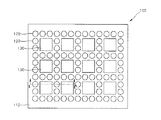
図1は、例示的な実施形態によるディスプレイ装置100を概略的に示す平面図である。そして、図2は、図1のI−I’線の断面図である。
FIG. 1 is a plan view schematically illustrating a
図1及び図2を参照すれば、ディスプレイ装置100は、基板110と、前記基板110上に設けられるOLED表示素子及びLCD素子とを備える。前記OLED表示素子は、基板110上に配置される複数のOLEDピクセル120を備え、前記LCD素子は、基板100上でOLEDピクセル120の間に配置される複数のLEDピクセル130を備える。ここで、前記LEDピクセル130は、LEDを光源として使うバックライトユニットを備える。前記基板110としては、多様な材質の基板が使われる。例えば、前記基板110として、プラスチック基板のような柔軟な材質の基板が使われてもよく、またガラス基板のような硬い材質の基板が使われてもよい。前記OLEDピクセル120及び前記LEDピクセル130が基板110の同一平面上に配置される。前記OLEDピクセル120それぞれは所定の原色光(すなわち、赤色光、緑色光または青色光)を出射する。例えば、いずれか一つのOLEDピクセル120が赤色光を出射する赤色ピクセルである場合、この赤色ピクセルの周りに配置するOLEDピクセル120は、緑色光を出射する緑色ピクセル及び青色光を出射する青色ピクセルになる。そして、前記LEDピクセル130は青色光を出射する。
Referring to FIGS. 1 and 2, the
図3は、図2に示されたOLEDピクセル120の断面図である。図3を参照すれば、OLEDピクセル120は、互いに離隔して配置される第1電極121及び第2電極122と、前記第1電極121と前記第2電極122との間に設けられる有機発光層123とを備える。前記第1電極121及び前記第2電極122は、アノード電極及びカソード電極になる。この場合、前記第1電極121は、例えば、ITO(Indium Tin Oxide)、IZO(Indium Zinc Oxide)、SnO2またはZnOなどの透明な導電性物質を含むが、これらに限定されるものではない。そして、前記第2電極122は、例えば、Al、Ag、Mg、LiまたはCaなどの金属やこれらの合金を含むが、これらに限定されるものではない。一方、前記第1電極121及び前記第2電極122がカソード電極及びアノード電極になってもよい。前記第1電極121及び前記第2電極122のうちいずれか一つの電極は共通電極になり、他の一つの電極は画素電極になる。この場合、前記画素電極は、OLEDピクセル120を選択的に駆動できる薄膜トランジスタ(図示せず)と連結される。
FIG. 3 is a cross-sectional view of the
前記第1電極121と前記第2電極122との間には、所定の原色光を発生させる有機発光層123が設けられている。前記有機発光層123は、例えば、赤色発光層、緑発光層または青色発光層になる。薄膜トランジスタの駆動によって第1電極121と第2電極122との間に電流が流れれば、アノード電極である第1電極121から有機発光層で正孔が流れ込み、カソード電極である第2電極122から有機発光層に電子が流れ込むことで、前記有機発光層123内で正孔と電子とが結合して所定色相の光(例えば、赤色光、緑色光または青色光)が放出される。このように放出される所定色相の光は、第2電極122を通じて外部に出射される。前記基板110上には、有機発光層123から放出された所定色相の光を第2電極122側に反射させるための反射板(図示せず)が設けられてもよい。そして、図示されていないが、アノード電極である第1電極121と有機発光層123との間には、正孔注入層及び/または正孔輸送層がさら設けられ、カソード電極である第2電極122と有機発光層123との間には、電子注入層及び/または電子輸送層がさらに設けられる。
Between the
図4には、図2に示されたOLEDピクセル120の変形例が示されている。図4を参照すれば、OLEDピクセル120’は互いに離隔して配置される第1電極121’及び第2電極122’と、前記第1電極121’と前記第2電極122’との間に設けられる白色有機発光層123’と、前記第2電極122’上に設けられるカラーフィルタ124’とを備える。前記白色有機発光層123’は、第1電極121’と第2電極122’との間に電流が印加されることで白色光を放出するものであり、複数の発光層(例えば、赤色、緑色及び青色の発光層)が積層された構造を持つ。そして、前記カラーフィルタ124’は、白色有機発光層123’から入射された白色光のうち所定色相の光(例えば、赤色光、緑色光または青色光)のみを透過させて外部に出射する。
FIG. 4 shows a modification of the
図5は、図2に示されたLEDピクセル130の断面図である。図4を参照すれば、LEDピクセル130は、白色光を出射する白色バックライトユニット131と、前記白色バックライトユニット131から入射された白色光を用いて選択的に青色光を放出する液晶パネル132と、を備える。前記白色バックライトユニット131は、LED光源を備える。具体的に、前記白色バックライトユニット131は、青色光を放出する青色LED光源と、前記青色LED光源から放出された青色光によって励起されて、それぞれ赤色光及び緑色光を放出する赤色量子点及び緑色量子点とを備える。このように、白色バックライトユニット131が、青色LED光源と、赤色量子点及び緑色量子点とを備える場合には、赤色に対する感度を高めることで色再現性を向上させる。一方、前記白色バックライトユニット131は、赤色、緑色及び青色のLED光源を備えるか、またはUV LED光源と赤色、緑色及び青色の蛍光体とを備える。また、前記白色バックライトユニット131は、青色LED光源及び黄色蛍光体を備えてもよい。
FIG. 5 is a cross-sectional view of the
前記白色バックライトユニット131から出射される白色光は、液晶パネル132側に入射される。前記液晶パネル132は、第1偏光板133、液晶層134、第2偏光板135及び青色カラーフィルタ136を備える。ここで、前記液晶層134は、光シャッターの役割を行うものであり、前記第1偏光板133を透過した白色光を選択的に透過させる役割を行う。前記液晶層134の駆動のために液晶層134の上下面には電極(図示せず)が設けられており、前記電極のうちいずれか一つは薄膜トランジスタと連結されている。そして、前記青色カラーフィルタ136は、液晶層134を通過した白色光のうち青色光のみを透過させて外部に出射させる。これによって、前記LEDピクセル130から青色光が出射される。
White light emitted from the
図6には、図2に示されたLEDピクセル130の変形例が示されている。図6を参照すれば、LEDピクセル130’は、青色光を出射する青色バックライトユニット131’と、前記青色バックライトユニット131’から入射された青色光を選択的に透過させる液晶パネル132’と、を備える。前記青色バックライトユニット131’は、青色LED光源を備える。前記青色バックライトユニット131’から出射される青色光は、液晶パネル132’側に入射される。前記液晶パネル132’は、第1偏光板133’、液晶層134’及び第2偏光板135’を備える。ここで、前記液晶層134’は、光シャッターの役割を行うものであり、第1偏光板133’を透過した青色光を選択的に透過させる役割を行う。これによって、前記LEDピクセル130’から青色光が出射される。
FIG. 6 shows a modification of the
以上のように、本実施形態によるディスプレイ装置100では、同じ基板110上に複数のOLEDピクセル120、120’と、複数のLEDピクセル130、130’とが配列されている。ここで、前記OLEDピクセル120、120’は、赤色光R、緑色光G及び青色光Bを出射し、前記LEDピクセル130、130’は、青色光Bを出射する。一般的に、OLED表示素子は、高精密発光可能で柔軟なディスプレイを具現できるという長所はあるが、青色に対する色再現性が少し劣り、青色ピクセルの寿命の短くなるという短所がある。本実施形態は、青色光を出射するLEDピクセル130を用いてOLED表示素子の青色ピクセルに対する問題点を補う。すなわち、本実施形態によるディスプレイ装置では、基板110上に赤色光R、緑色光G及び青色光Bを出射する複数のOLEDピクセル120を配置し、このOLEDピクセル120の間に青色光Bを出射する複数のLEDピクセル130を配置する。ここで、前記OLEDピクセル120は、イメージを形成する役割を行い、前記LEDピクセル130は、青色光を出射するOLEDピクセル120を補うか、または取り替える役割を行う。これによって、イメージの青色に対する色再現性を向上させられるので、実際イメージに最大限近いイメージが具現される。また、ディスプレイ装置100の寿命も延びる。さらに、LEDピクセル130の白色バックライトユニット131を青色LED光源と赤色量子点及び緑色量子点とで構成する場合には、色再現性をさらに向上させる。一方、図1には、LEDピクセル130がOLEDピクセル120の間に規則的な形態に配列される場合が示されているが、前記LEDピクセル130は、ランダムな形態に配列されてもよい。
As described above, in the
図7は、他の例示的な実施形態によるディスプレイ装置200を示す断面図である。図7に示されたディスプレイ装置200の平面図は、図1と同一である。以下では、前述した実施形態と異なる点を中心として説明する。
FIG. 7 is a cross-sectional view illustrating a
図7を参照すれば、ディスプレイ装置200は、基板210上に設けられる複数のOLEDピクセル220及び複数のLEDピクセル230を備える。このようなOLEDピクセル220及びLEDピクセル230は、基板210の同一平面上に配置される。前記OLEDピクセル220は、赤色光R、緑色光G及び青色光Bを出射する。前記OLEDピクセル220は、前述した図3に示されたOLEDピクセル120や図4に示されたOLEDピクセル120’と同一であるので、これに関する説明は略する。本実施形態で、前記LEDピクセル230は、白色光Wを出射する。
Referring to FIG. 7, the
図8は、図7に示されたLEDピクセル230の断面図である。図8を参照すれば、LEDピクセル230は、白色光を出射する白色バックライトユニット231と、前記白色バックライトユニット231から入射された白色光を選択的に透過させる液晶パネル232と、を備える。前記白色バックライトユニット231は、LED光源を備える。具体的に、前記白色バックライトユニット231は、青色光を放出する青色LED光源と、前記青色LED光源から放出された青色光によって励起されてそれぞれ赤色光及び緑色光を放出する赤色量子点及び緑色量子点と、を備える。このように、白色バックライトユニット231が青色LED光源と、赤色量子点及び緑色量子点とを備える場合には、赤色に対する感度を向上させて色再現性を向上させる。一方、前記白色バックライトユニット231は、赤色、緑色及び青色のLED光源を備えるか、または前記白色バックライトユニット231は、UV LED光源と赤色、緑色及び青色の蛍光体とを備える。また、前記白色バックライトユニット231は、青色LED光源と黄色蛍光体とを備えることもできる。
FIG. 8 is a cross-sectional view of the
前記白色バックライトユニット231から出射される白色光は、液晶パネル232側に入射される。前記液晶パネル232は、第1偏光板233、液晶層234及び第2偏光板235を備える。ここで、前記液晶層234は、光シャッターの役割を行うものであり、入射される白色光を選択的に透過させる役割を行う。前記液晶層234の駆動のために液晶層234の上下面には電極(図示せず)が設けられており、前記電極のうちいずれか一つは薄膜トランジスタと連結されている。これによって、前記LEDピクセル230から白色光Wが出射される。
White light emitted from the
OLED表示素子は、輝度において限界があり、これにより電力消耗及び寿命短縮が問題になる。本実施形態では、白色光を出射するLEDピクセル230を用いてOLED表示素子の輝度及び寿命問題を補う。すなわち、本実施形態によるディスプレイ装置では、基板210上に赤色光R、緑色光G及び青色光Bを出射する複数のOLEDピクセル220を配置し、このOLEDピクセル220の間に白色光Wを出射する複数のLEDピクセル230を配置する。ここで、前記OLEDピクセル220は、イメージを形成する役割を行い、前記LEDピクセル230は、イメージを明るくする役割を行う。これによって、ディスプレイ装置200の輝度を向上させられ、その寿命も延びる。さらに、前記LEDピクセル230の白色バックライトユニット231を青色LED光源と、赤色量子点及び緑色量子点で構成する場合には、白色に対する色再現性をさらに向上させる。一方、前記LEDピクセル230は、OLEDピクセル220の間に規則的な形態に配列されるか、またはランダムな形態に配列される。
The OLED display element has a limit in luminance, which causes problems of power consumption and shortening of life. In the present embodiment, the
図9は、他の例示的な実施形態によるディスプレイ装置300を示す断面図である。図9に示されたディスプレイ装置300の平面図は、図1と同一である。以下では、前述した実施形態と異なる点を中心として説明する。
FIG. 9 is a cross-sectional view illustrating a
図9を参照すれば、ディスプレイ装置300は、基板310上に設けられる複数のOLEDピクセル320及び複数のLEDピクセル330を備える。このようなOLEDピクセル320及びLEDピクセル330は、基板310の同一平面上に配置される。本実施形態で、前記OLEDピクセル320は、白色光Wを出射し、前記LEDピクセル330は、赤色光R、緑色光G及び青色光Bを出射する。前記LEDピクセル330それぞれは、所定の原色光(すなわち、赤色光、緑色光または青色光)を出射する。例えば、いずれか一つのLEDピクセル330が、赤色光を出射する赤色ピクセルである場合、この赤色ピクセルの周りにあるLEDピクセル330は、緑色光を出射する緑色ピクセル及び青色光を出射する青色ピクセルになる。
Referring to FIG. 9, the
図10は、図9に示されたOLEDピクセル320の断面図である。図10を参照すれば、OLEDピクセル320は、互いに離隔して配置される第1電極321及び第2電極322と、前記第1電極321と前記第2電極322との間に設けられる白色有機発光層323と、を備える。前記第1電極321及び前記第2電極322は、アノード電極及びカソード電極になる。一方、前記第1電極321及び前記第2電極322がカソード電極及びアノード電極になってもよい。前記第1電極321及び第2電極322のうちいずれか一つの電極は共通電極になり、他の一つの電極は画素電極になる。この場合、前記画素電極は、OLEDピクセル320を選択的に駆動できる薄膜トランジスタ(図示せず)と連結される。
FIG. 10 is a cross-sectional view of the
前記第1電極321と前記第2電極322との間には、白色光を発生させる白色有機発光層323が設けられている。白色有機発光層323は、第1電極321と第2電極322との間に電流が印加されることで白色光を放出するものであり、複数の発光層(例えば、赤色、緑色及び青色の発光層)が積層された構造を持つ。一方、前記基板310上には、白色有機発光層323から放出された白色光を第2電極322側に反射させるための反射板(図示せず)が設けられてもよい。そして、図面には示されていないが、アノード電極である第1電極321と白色有機発光層323との間には正孔注入層及び/または正孔輸送層がさらに設けられ、カソード電極である第2電極322と白色有機発光層323との間には電子注入層及び/または電子輸送層がさらに設けられる。
A white organic
図11は、図9に示されたLEDピクセル330の断面図である。図11を参照すれば、LEDピクセル330は、白色光を出射する白色バックライトユニット331と、前記白色バックライトユニット331から入射された白色光を用いて所定の原色光(赤色光、緑色光または青色光)を選択的に放出する液晶パネル332と、を備える。前記白色バックライトユニット331は、LED光源を備える。具体的に、前記白色バックライトユニット331は、青色光を放出する青色LED光源と、前記青色LED光源から放出された青色光によって励起されてそれぞれ赤色光及び緑色光を放出する赤色量子点及び緑色量子点と、を備える。このように、白色バックライトユニット331が青色LED光源と、赤色量子点及び緑色量子点とを備える場合には、赤色に対する感度を高めることで色再現性を向上させる。一方、前記白色バックライトユニット331は、赤色、緑色及び青色のLED光源を備えるか、またはUV LED光源と赤色、緑色及び青色の蛍光体とを備える。また、前記白色バックライトユニット331は、青色LED光源及び黄色蛍光体を備えてもよい。
11 is a cross-sectional view of the
前記白色バックライトユニット331から出射される白色光は、液晶パネル332側に入射される。前記液晶パネル332は、第1偏光板333、液晶層334、第2偏光板335、及びカラーフィルタ336を備える。ここで、前記液晶層334は、光シャッターの役割を行うものであり、前記第1偏光板333を透過した白色光を選択的に透過させる役割を行う。前記液晶層334の駆動のために、液晶層334の上下面には電極(図示せず)が設けられており、前記電極のうちいずれか一つは薄膜トランジスタと連結されている。そして、前記カラーフィルタ336は、液晶層334を通過した白色光のうち所定の原色光のみを透過させて外部に出射させる。例えば、前記カラーフィルタ336が赤色カラーフィルタである場合には、液晶層334を通過した白色光のうち赤色光のみがカラーフィルタ336を透過して外部に放出される。そして、前記カラーフィルタ336が緑色カラーフィルタである場合には、液晶層334を通過した白色光のうち緑色光のみが、カラーフィルタ336を透過して外部に放出され、前記カラーフィルタ336が青色カラーフィルタである場合には、液晶層334を通過した白色光のうち青色光のみが、カラーフィルタ336を透過して外部に放出される。
White light emitted from the
図12には、図9に示されたLEDピクセル330の変形例が示されている。図12を参照すれば、LEDピクセル330’は、所定の原色光(赤色光、緑色光または青色光)を出射するバックライトユニット331’と、前記バックライトユニット331’から入射された所定の原色光を選択的に透過させる液晶パネル332’と、を備える。前記バックライトユニット331’は、LED光源を備える。具体的に、前記バックライトユニット331’は、赤色LED光源、緑色LED光源または青色LED光源を備える。前記バックライトユニット331’から出射される所定色相の光は、液晶パネル332’側に入射される。前記液晶パネル332’は、第1偏光板333’、液晶層334’、及び第2偏光板335’を備える。ここで、前記液晶層334’は、光シャッターの役割を行うものであり、第1偏光板333’を透過した所定色相の光を選択的に透過させる役割を行う。前記液晶層334’の駆動のために、液晶層334’の上下面には電極(図示せず)が設けられており、前記電極のうちいずれか一つは、薄膜トランジスタと連結されている。
FIG. 12 shows a modification of the
本実施形態によるディスプレイ装置300では、基板310上に白色光Wを放出する複数のOLEDピクセル320を配置し、このOLEDピクセル320の間に赤色光R、緑色光G及び青色光Bを出射する複数のLEDピクセル330、330’を配置する。ここで、前記LEDピクセル330、330’は、イメージを形成する役割を行い、前記OLEDピクセル320は、イメージを明るくする役割を行う。これによって、ディスプレイ装置300の輝度を向上させる。さらに、前記LEDピクセル330の白色バックライトユニット331を青色LED光源と、赤色量子点及び緑色量子点とで構成する場合には、白色に対する色再現性をさらに向上させる。一方、前記OLEDピクセル320は、LEDピクセル330及び330’の間に規則的な形態に配列されるか、またはランダムな形態に配列される。
In the
図13は、他の例示的な実施形態によるディスプレイ装置400を概略的に示す平面図である。そして、図14は、図1のII−II’線の断面図である。
FIG. 13 is a plan view schematically showing a
図13及び図14を参照すれば、ディスプレイ装置400は、垂直に積層されたOLED表示素子及びLCD素子を備える。第1基板420及び第2基板460が互いに対向して離隔して設けられている。ここで、前記第1基板420は、第2基板460よりディスプレイ装置400の前面側に配置される。前記OLED表示素子は、第1基板420上に設けられており、前記LCD素子は、第2基板460上に設けられている。前記第1基板420及び前記第2基板460としては、多様な材質の基板が使われる。例えば、前記第1基板420及び前記第2基板460として、プラスチック基板のような柔軟な材質の基板が使われてもよく、またガラス基板のような硬い材質の基板が使われてもよい。
13 and 14, the
前記OLED表示素子は、第1基板420上に配置される複数のOLEDピクセル430及び複数のブランクピクセル440を備える。そして、前記LCD素子は、第2基板460上に配置される複数のLEDピクセル470を備え、前記LEDピクセル470は、LEDを光源として使うバックライトユニットを備える。ここで、前記LEDピクセル470は、前記ブランクピクセル440に対応して設けられる。
The OLED display device includes a plurality of
前記OLEDピクセル430は、第1基板420上に所定形態に配列されており、前記ブランクピクセル440は、OLEDピクセル430の間に所定形態に配列されている。前記OLEDピクセル430それぞれは、所定の原色光(すなわち、赤色光、緑色光または青色光)を出射する。例えば、いずれか一つのOLEDピクセル430が赤色光を出射する赤色ピクセルである場合、この赤色ピクセルの周りにあるOLEDピクセル430は、緑色光を出射する緑色ピクセル及び青色光を出射する青色ピクセルになる。前記ブランクピクセル440は、後述するLEDピクセル470から出射される青色光を透過させるピクセルを意味する。よって、前記LEDピクセル470から放出される青色光は、ブランクピクセル440を透過して外部に出射される。ここで、前記ブランクピクセル440は、例えば、第1基板420上に貫通孔420aを形成することで設けられる。このようなブランクピクセル440は、OLEDピクセル430の間に規則的な形態に配列されるか、またはランダムな形態に配列される。
The
前記LEDピクセル470は、第2基板460上に所定形態に配列されている。ここで、前記LEDピクセル470は、前述したブランクピクセル440に対応する位置に設けられる。これによって、前記LEDピクセル470は、ブランクピクセル440と同じ形態に配列される。前記LEDピクセル470は、青色光を出射する。
The
図15は、図14に示されたOLEDピクセル430の断面図である。図15を参照すれば、OLEDピクセル430は、互いに離隔して配置される第1電極431及び第2電極432と、前記第1電極431と前記第2電極432との間に設けられる有機発光層433と、を備える。前記第1電極431及び第2電極432は、アノード電極及びカソード電極になる。この場合、前記第1電極431は、例えば、ITO、IZO、SnO2またはZnOなどのような透明な導電性物質を含むが、これらに限定されるものではない。そして、前記第2電極432は、例えば、Al、Ag、Mg、LiまたはCaなどのような金属や、これらの合金を含むが、これらに限定されるものではない。一方、前記第1電極431及び前記第2電極432がカソード電極及びアノード電極になってもよい。前記第1電極431及び第2電極432のうちいずれか一つの電極は共通電極になり、他の一つの電極は画素電極になる。この場合、前記画素電極は、OLEDピクセル430を駆動できる薄膜トランジスタと連結される。
FIG. 15 is a cross-sectional view of the
前記第1電極431及び前記第2電極432との間には、所定の原色光を発生させる有機発光層433が設けられている。前記有機発光層433は、例えば、赤色発光層、緑発光層または青色発光層になる。薄膜トランジスタの駆動によって第1電極431と第2電極432との間に電流が流れれば、アノード電極である第1電極431から有機発光層に正孔が流れ込み、カソード電極である第2電極432から有機発光層に電子が流れ込むことで、前記有機発光層433内で正孔と電子とが結合して所定色相の光(例えば、赤色光、緑色光または青色光)が放出される。このように放出される所定色相の光は、第2電極432を通じて外部に出射される。前記基板420上には、有機発光層433から放出された所定色相の光を第2電極432側に反射させるための反射板(図示せず)が設けられてもよい。そして、図面には示されていないが、アノード電極である第1電極431と有機発光層433との間には正孔注入層及び/または正孔輸送層がさらに設けられ、カソード電極である第2電極432と有機発光層433との間には電子注入層及び/または電子輸送層がさらに設けられる。
Between the
図16には、図14に示されたOLEDピクセル430の変形例が示されている。図16を参照すれば、OLEDピクセル430’は、互いに離隔して配置される第1電極431’及び第2電極432’と、前記第1電極431’と前記第2電極432’との間に設けられる白色有機発光層433’と、前記第2電極432’上に設けられるカラーフィルタ434’と、を備える。前記白色有機発光層433’は、第1電極431’と第2電極432’との間に電流が印加されることで白色光を放出するものであり、複数の発光層(例えば、赤色、緑色及び青色の発光層)が積層された構造を持つ。そして、前記カラーフィルタ434’は、白色有機発光層433’から入射された白色光のうち所定色相の光(例えば、赤色光、緑色光または青色光)のみを透過させて外部に出射する。
FIG. 16 shows a modification of the
図17は、図14に示されたLEDピクセル470の断面図である。図17を参照すれば、LEDピクセル470は、白色光を出射する白色バックライトユニット471と、前記白色バックライトユニット471から入射された白色光を用いて選択的に青色光を放出する液晶パネル472と、を備える。前記白色バックライトユニット471はLED光源を備える。具体的に、前記白色バックライトユニット471は、青色光を放出する青色LED光源と、前記青色LED光源から放出された青色光によって励起されて、それぞれ赤色光及び緑色光を放出する赤色量子点及び緑色量子点と、を備える。このように、白色バックライトユニット471が青色LED光源と、赤色量子点及び緑色量子点とを備える場合には、赤色に対する感度を高めることで色再現性を向上させる。一方、前記白色バックライトユニット471は、赤色、緑色及び青色のLED光源を備えるか、またはUV LED光源と赤色、緑色及び青色の蛍光体とを備える。また、前記白色バックライトユニット471は、青色LED光源及び黄色蛍光体を備えてもよい。
FIG. 17 is a cross-sectional view of the
前記白色バックライトユニット471から出射される白色光は、液晶パネル472側に入射される。前記液晶パネル472は、第1偏光板473、液晶層474、第2偏光板475、及び青色カラーフィルタ476を備える。ここで、前記液晶層474は、光シャッターの役割を行うものであり、第1偏光板473を透過した白色光を選択的に透過させる役割を行う。前記液晶層474の駆動のために液晶層474の上下面には電極(図示せず)が設けられており、前記電極のうちいずれか一つは薄膜トランジスタと連結されている。そして、前記青色カラーフィルタ476は、液晶層474を通過した白色光のうち青色光のみを透過させて外部に出射させる。これによって、前記LEDピクセル470から青色光が出射される。
White light emitted from the
図18には、図14に示されたLEDピクセル470の変形例が示されている。図18を参照すれば、LEDピクセル470’は、青色光を出射する青色バックライトユニット471’と、前記青色バックライトユニット471’から入射された青色光を選択的に透過させる液晶パネル472’と、を備える。前記青色バックライトユニット471’は、青色LED光源を備える。前記青色バックライトユニット471’から出射される青色光は、液晶パネル472’側に入射される。前記液晶パネル472’は、第1偏光板473’、液晶層474’及び第2偏光板475’を備える。ここで、前記液晶層474’は、光シャッターの役割を行うものであり、前記第1偏光板473’を透過した青色光を選択的に透過させる役割を行う。これによって、前記LEDピクセル470’から青色光が出射される。
FIG. 18 shows a modification of the
以上のように、本実施形態によるディスプレイ装置400は、OLED表示素子及びLCD素子が垂直に積層された構造を持っている。具体的に、第1基板420上に複数のOLEDピクセル430及び複数のブランクピクセル440が配置され、前記第2基板460上には、複数のLEDピクセル470、470’が前記ブランクピクセル440と対応して配列されている。ここで、前記OLEDピクセル430は、赤色光R、緑色光G及び青色光Bを出射し、前記LEDピクセル470、470’は、青色光Bを出射する。ここで、前記LEDピクセル470、470’から放出される青色光Bは、第1基板420上に設けられたブランクピクセル440を透過して外部に出射される。OLED表示素子は、青色に対する色再現性が少し劣り、青色ピクセルの寿命が短くなるという短所があるところ、本実施形態は、青色光を出射するLEDピクセル470、470’を用いてOLED表示素子の青色ピクセルに対する問題点を補うことができる。すなわち、本実施形態によるディスプレイ装置では第1基板420上に赤色光R、緑色光G及び青色光Bを出射する複数のOLEDピクセル430及び青色光を透過させる複数のブランクピクセル440を配置して、第2基板460上に青色光Bを出射する複数のLEDピクセル470をブランクピクセル440に対応するように配置する。ここで、前記LEDピクセル470から放出される青色光Bは、ブランクピクセル440を通じて外部に出射される。前記OLEDピクセル430は、イメージを形成する役割を行い、前記ブランクピクセル440を透過する青色光Bを放出するLEDピクセル470、470’は、青色光を出射するOLEDピクセル430を補うか、または取り替える役割を行う。これによって、イメージの青色に対する色再現性を向上させられるので、実際イメージに最大限近いイメージが具現される。また、ディスプレイ装置400の寿命も延びる。さらに、LEDピクセル470の白色バックライトユニット471を青色LED光源と赤色量子点及び緑色量子点とで構成する場合には、色再現性をさらに向上させる。
As described above, the
図19は、他の例示的な実施形態によるディスプレイ装置500を示す断面図である。図19に示されたディスプレイ装置500の平面図は、図13と同一である。以下では、前述した実施形態と異なる点を中心として説明する。 FIG. 19 is a cross-sectional view illustrating a display device 500 according to another exemplary embodiment. A plan view of the display device 500 shown in FIG. 19 is the same as FIG. Below, it demonstrates centering on a different point from embodiment mentioned above.
図19を参照すれば、第1基板520及び第2基板560が互いに対向して離隔して設けられている。前記第1基板520は、第2基板560よりディスプレイ装置500の前面側に配置される。前記第1基板520上にはOLED表示素子が設けられており、前記第2基板560上にはLCD素子が設けられている。前記OLED表示素子は、第1基板520上に配置される複数のOLEDピクセル530及び複数のブランクピクセル540を備える。そして、前記LCD素子は、第2基板560上に配置される複数のLEDピクセル570を備え、前記LEDピクセル570は、LEDを光源として使うバックライトユニットを備える。ここで、前記LEDピクセル570は、ブランクピクセル540に対応して設けられる。
Referring to FIG. 19, a first substrate 520 and a
前記OLEDピクセル530は、第1基板520上に所定形態に配列されており、前記ブランクピクセル540は、OLEDピクセル530の間に所定形態に配列されている。前記OLEDピクセル530それぞれは、所定の原色光(すなわち、赤色光、緑色光または青色光)を出射する。例えば、いずれか一つのOLEDピクセル530が赤色光を出射する赤色ピクセルである場合、この赤色ピクセルの周りにあるOLEDピクセル530は、緑色光を出射する緑色ピクセル及び青色光を出射する青色ピクセルになる。前記OLEDピクセル530は、前述した図15に示されたOLEDピクセル430や、図16に示されたOLEDピクセル430’と同一であるので、これに関する説明は略する。前記ブランクピクセル540は、後述するLEDピクセル570から出射される白色光を透過させるピクセルを意味する。よって、前記LEDピクセル570から放出される白色光は、ブランクピクセル540を透過して外部に出射される。前記ブランクピクセル540は、第1基板520上に貫通孔520aを形成することで設けられる。これらのブランクピクセル540は、OLEDピクセル530の間に規則的な形態に配列されるか、またはランダムな形態に配列される。前記LEDピクセル570は、第2基板560上にブランクピクセル540に対応する位置に設けられる。これによって、前記LEDピクセル570は、ブランクピクセル540と同じ形態に配列される。前記LEDピクセル570は、白色光を出射する。
The
図20は、図19に示されたLEDピクセル570の断面図である。図20を参照すれば、LEDピクセル570は、白色光を出射する白色バックライトユニット571と、前記白色バックライトユニット571から入射された白色光を選択的に透過させる液晶パネル572とを備える。前記白色バックライトユニット571は、LED光源を備える。具体的に、前記白色バックライトユニット571は、青色光を放出する青色LED光源と、前記青色LED光源から放出された青色光によって励起されてそれぞれ赤色光及び緑色光を放出する赤色量子点及び緑色量子点と、を備える。このように、白色バックライトユニット571が青色LED光源と、赤色量子点及び緑色量子点とを備える場合には、赤色に対する感度を向上させて色再現性を向上させる。一方、前記白色バックライトユニット571は、赤色、緑色及び青色のLED光源を備えるか、またはUV LED光源と赤色、緑色及び青色の蛍光体を備える。また、前記白色バックライトユニット571は、青色LED光源及び黄色蛍光体を備えてもよい。
20 is a cross-sectional view of the
前記白色バックライトユニット571から出射される白色光は、液晶パネル572側に入射される。前記液晶パネル572は、第1偏光板573、液晶層574及び第2偏光板575を備える。ここで、前記液晶層574は、光シャッターの役割を行うものであり、入射される白色光を選択的に透過させる役割を行う。前記液晶層574の駆動のために液晶層574の上下面には電極(図示せず)が設けられており、前記電極のうちいずれか一つは薄膜トランジスタと連結されている。これによって、前記LEDピクセル570から白色光が出射される。
White light emitted from the
本実施形態では、白色光を出射するLEDピクセル570を用いてOLED表示素子の輝度及び寿命問題を補う。すなわち、本実施形態によるディスプレイ装置500では、第1基板520上に赤色光R、緑色光G及び青色光Bを出射する複数のOLEDピクセル530及び白色光Wを透過させる複数のブランクピクセル540を配置し、第2基板560上にブランクピクセル540に対応する複数のLEDピクセル570を配置する。ここで、前記LEDピクセル570から放出された白色光Wは、ブランクピクセル540を通じて外部に出射される。前記OLEDピクセル530は、イメージを形成する役割を行い、前記ブランクピクセル540を透過する白色光Wを放出するLEDピクセル570は、イメージを明るくする役割を行う。これによって、ディスプレイ装置500の輝度を向上させ、その寿命も延ばせる。さらに、前記LEDピクセル570の白色バックライトユニット571を、青色LED光源と、赤色量子点及び緑色量子点とで構成する場合には、白色に対する色再現性をさらに向上させ得る。
In this embodiment, the
図21は、他の例示的な実施形態によるディスプレイ装置600を示す断面図である。図21に示されたディスプレイ装置600の平面図は、図13と同一である。以下では、前述した実施形態と異なる点を中心として説明する。
FIG. 21 is a cross-sectional view illustrating a
図21を参照すれば、第1基板620及び第2基板660が互いに対向して離隔して設けられている。前記第1基板620は、第2基板660よりディスプレイ装置600の前面側に配置される。前記第1基板620上には、OLED表示素子が設けられており、前記第2基板660上にはLCD素子が設けられている。前記OLED表示素子は、第1基板620上に配置される複数のOLEDピクセル630及び複数のブランクピクセル640を備える。そして、前記LCD素子は、第2基板660上に配置される複数のLEDピクセル670を備え、前記LEDピクセル670は、LEDを光源として使うバックライトユニットを備える。ここで、前記LEDピクセル670は、ブランクピクセル640に対応して設けられる。
Referring to FIG. 21, a
前記OLEDピクセル630は、第1基板620上に配列されており、前記ブランクピクセル640は、前記OLEDピクセル630の間に配列されている。前記OLEDピクセル630は、白色光を出射し、前記ブランクピクセル640は、後述するLEDピクセル670から放出される所定の原色光(赤色光、緑色光または青色光)を透過させる。前記LEDピクセル670は、第2基板660上にブランクピクセル640と対応して配列されている。前記LEDピクセル670は、赤色光R、緑色光G及び青色光Bを出射する。前記LEDピクセル670それぞれは、所定の原色光(すなわち、赤色光、緑色光または青色光)を出射する。例えば、いずれか一つのLEDピクセル670が、赤色光を出射する赤色ピクセルである場合、この赤色ピクセルの周りにあるLEDピクセル670は、緑色光を出射する緑色ピクセル及び青色光を出射する青色ピクセルになる。
The
図22は、図21に示されたOLEDピクセル630の断面図である。図22を参照すれば、OLEDピクセル630は、互いに離隔して配置される第1電極631及び第2電極632と、前記第1電極631と前記第2電極632との間に設けられる白色有機発光層633と、を備える。前記第1電極631及び前記第2電極632は、アノード電極及びカソード電極になる。一方、前記第1電極631及び前記第2電極632がカソード電極及びアノード電極になってもよい。前記第1電極631及び前記第2電極632のうちいずれか一つの電極は共通電極になり、他の一つの電極は画素電極になる。この場合、前記画素電極は、OLEDピクセル630を選択的に駆動できる薄膜トランジスタ(図示せず)と連結される。
FIG. 22 is a cross-sectional view of the
前記第1電極631と前記第2電極632との間には、白色光を発生させる白色有機発光層633が設けられている。前記白色有機発光層633は、第1電極631と前記第2電極632との間に電流が印加されることで白色光を放出するものであり、複数の発光層(例えば、赤色、緑色及び青色の発光層)が積層された構造を持つ。一方、前記第1基板620上には、白色有機発光層633から放出された白色光を第2電極632側に反射させるための反射板(図示せず)が設けられてもよい。そして、図面には示されていないが、アノード電極である第1電極631と白色有機発光層633との間には、正孔注入層及び/または正孔輸送層がさらに設けられ、カソード電極である第2電極632と白色有機発光層633との間には電子注入層及び/または電子輸送層がさらに設けられる。
A white organic
図23は、図21に示されたLEDピクセル670の断面図である。図23を参照すれば、LEDピクセル670は、白色光を出射する白色バックライトユニット671と、前記白色バックライトユニット671から入射された白色光を用いて所定の原色光(赤色光、緑色光または青色光)を放出する液晶パネル672と、を備える。前記白色バックライトユニット671は、LED光源を備える。具体的に、前記白色バックライトユニット671は、青色光を放出する青色LED光源と、前記青色LED光源から放出された青色光によって励起されてそれぞれ赤色光及び緑色光を放出する赤色量子点及び緑色量子点と、を備える。このように、白色バックライトユニット671が青色LED光源と、赤色量子点及び緑色量子点とを備える場合には、赤色に対する感度を高めることで色再現性を向上させる。一方、前記白色バックライトユニット671は、赤色、緑色及び青色のLED光源を備えるか、またはUV LED光源と赤色、緑色及び青色の蛍光体とを備える。また、前記白色バックライトユニット671は、青色LED光源及び黄色蛍光体を備えてもよい。
FIG. 23 is a cross-sectional view of the
前記白色バックライトユニット671から出射される白色光は、液晶パネル672側に入射される。前記液晶パネル672は、第1偏光板673、液晶層674、第2偏光板675及びカラーフィルタ676を備える。ここで、前記液晶層674は、光シャッターの役割を行うものであり、前記第1偏光板673を透過した白色光を選択的に透過させる役割を行う。前記液晶層674の駆動のために、液晶層674の上下面には電極(図示せず)が設けられており、前記電極のうちいずれか一つは薄膜トランジスタと連結されている。そして、前記カラーフィルタ676は、液晶層674を通過した白色光のうち所定の原色光のみを透過させて外部に出射させる。例えば、前記カラーフィルタ676が赤色カラーフィルタである場合には、液晶層674を通過した白色光のうち赤色光のみがカラーフィルタ676を透過して外部に放出される。そして、前記カラーフィルタ676が緑色カラーフィルタである場合には、液晶層674を通過した白色光のうち緑色光のみがカラーフィルタ676を透過して外部に放出され、前記カラーフィルタ676が青色カラーフィルタである場合には、液晶層674を通過した白色光のうち青色光のみがカラーフィルタ676を透過して外部に放出される。
White light emitted from the
図24には、図21に示されたLEDピクセル670の変形例が示されている。図24を参照すれば、LEDピクセル670’は、所定の原色光(赤色光、緑色光または青色光)を出射するバックライトユニット671’と、前記バックライトユニット671’から入射された所定の原色光を選択的に透過させる液晶パネル672’と、を備える。前記バックライトユニット671’は、LED光源を備える。具体的に、前記バックライトユニット671’は、赤色LED光源、緑色LED光源または青色LED光源を備える。前記バックライトユニット671’から出射される所定色相の光は、液晶パネル672’側に入射される。前記液晶パネル672’は、第1偏光板673’、液晶層674’、及び第2偏光板675’を備える。ここで、前記液晶層674’は、光シャッターの役割を行うものであり、前記第1偏光板673’を透過した所定色相の光を選択的に透過させる役割を行う。前記液晶層674’の駆動のために、液晶層674’の上下面には電極(図示せず)が設けられており、前記電極のうちいずれか一つは、薄膜トランジスタと連結されている。
FIG. 24 shows a modification of the
本実施形態によるディスプレイ装置600では、第1基板620上に白色光Wを放出する複数のOLEDピクセル630及び所定色相の光を透過させる複数のブランクピクセル640を配置し、第2基板660上に、ブランクピクセル640に対応して赤色光R、緑色光G及び青色光Bを出射する複数のLEDピクセル670、670’を配置する。ここで、前記LEDピクセル670、670’から放出される所定色相の光は、ブランクピクセル640を透過して外部に出射される。前記LEDピクセル670、670’は、イメージを形成する役割を行い、前記OLEDピクセル630は、イメージを明るくする役割を行う。これによって、ディスプレイ装置600の輝度を向上させる。さらに、前記LEDピクセル670の白色バックライトユニット671を、青色LED光源と、赤色量子点及び緑色量子点とで構成する場合には、白色に対する色再現性をさらに向上させ得る。一方、前記OLEDピクセル670、670’は、規則的な形態に配列されるか、またはランダムな形態に配列される。
In the
図25は、他の例示的な実施形態によるディスプレイ装置700を示す分離斜視図である。そして、図26は、図25のIII−III’線の断面図である。
FIG. 25 is an exploded perspective view illustrating a
図25及び図26を参照すれば、ディスプレイ装置700は、第1基板720及び第2基板760と、前記第1基板720上に配置されるものとして複数の赤色OLEDピクセル730R、緑色OLEDピクセル730G及びブランクピクセル735と、前記第1基板720と第2基板760との間に設けられるものとして第1貫通孔755が形成された反射板750と、前記第2基板760上に設けられる青色光放出ユニット770と、を備える。第1基板720及び第2基板760は、互いに対向して離隔して設けられている。ここで、前記第1基板720は、第2基板760よりディスプレイ装置700の前面側に配置される。前記第1基板720及び第2基板760としては、多様な材質の基板が使われる。例えば、前記第1基板720及び第2基板760として、プラスチック基板のような柔軟な材質の基板が使われてもよく、またガラス基板のような硬い材質の基板が使われてもよい。
Referring to FIGS. 25 and 26, the
前記第1基板720上には、複数の赤色OLEDピクセル730R、緑色OLEDピクセル730G及びブランクピクセル735が配置されている。ここで、前記赤色OELDピクセル730R、緑色OLEDピクセル730G及びブランクピクセル735は、順次に配置されている。前記赤色及び緑色のOLEDピクセル730R、730Gは、それぞれ赤色光、緑色光及び青色光を放出する。そして、前記ブランクピクセルは、青色光放出ユニット770から放出される青色光を透過させる。このために、前記ブランクピクセル735は、第1基板720に形成された第2貫通孔720aを備える。
A plurality of
図27A及び図27Bには、前記赤色及び緑色のOLEDピクセル730R、730Gの断面が示されている。図27A及び図27Bを参照すれば、赤色OLEDピクセル730Rは、第1電極731及び第2電極732と、前記第1電極731と第2電極732との間に設けられて赤色光を放出する赤色有機発光層733Rと、を備える。そして、緑色OLEDピクセル730Gは、前記第1電極731及び第2電極732と、前記第1電極731と前記第2電極732との間に設けられて緑色光を放出する緑有機発光層733Gと、を備える。
27A and 27B show cross sections of the red and
前記第1電極731及び前記第2電極732は、アノード電極及びカソード電極になる。この場合、前記第1電極731は、例えば、ITO、IZO、SnO2またはZnOなどの透明な導電性物質を含むが、これらに限定されるものではない。そして、前記第2電極732は、例えば、Al、Ag、Mg、LiまたはCaなどの金属やこれらの合金を含むが、これらに限定されるものではない。一方、前記第1電極731及び前記第2電極732がカソード電極及びアノード電極になってもよい。前記第1電極731及び前記第2電極732のうちいずれか一つの電極は、共通電極になり、他の一つの電極は画素電極になる。この場合、前記画素電極は、所定のOLEDピクセル730R、730Gを駆動できる所定薄膜トランジスタと連結される。
The
所定薄膜トランジスタの駆動によって第1電極731と第2電極732との間に電流が流れれば、アノード電極である第1電極731から所定の有機発光層733R、733Gに正孔が流れ込み、カソード電極である第2電極732から有機発光層733R、733Gに電子が流れ込むことで、前記有機発光層733R、733G内で正孔と電子とが結合して所定色相の光(赤色光または緑色光)が放出される。このように放出される所定色相の光は、第2電極732を通じて外部に出射される。一方、図面には示されていないが、アノード電極である第1電極731と有機発光層733R、733Gとの間には、正孔注入層及び/または正孔輸送層がさらに設けられ、カソード電極である第2電極732と有機発光層733R、733Gとの間には、電子注入層及び/または電子輸送層がさらに設けられる。
If a current flows between the
前記第1基板720の下部には反射板750が設けられている。ここで、前記反射板750は、赤色及び緑色のOLEDピクセル730R、730Gから放出される赤色光及び緑色光を第2電極732側に反射させる役割を行う。そして、前記反射板750には、ブランクピクセル735に対応する第1貫通孔755が形成されている。
A
前記第2基板760上には、青色光を放出する青色光放出ユニット770が設けられている。図28には、青色光放出ユニット770の断面が示されている。図28を参照すれば、青色光放出ユニット770は、青色光を出射する青色バックライトユニット771と、前記青色バックライトユニット771から入射された青色光を透過させる液晶パネル772とを備える。ここで、前記バックライトユニット771は、少なくとも一つの青色LED光源を備える。前記バックライトユニット771から出射される青色光は、液晶パネル772側に入射される。前記液晶パネル772は、第1偏光板773、液晶層774、及び第2偏光板775を備える。前記液晶層774は、光シャッターの役割を行うものであり、前記第1偏光板773を透過した青色光を選択的に透過させる役割を行う。具体的に、前記液晶層774は、ブランクピクセル735に対応する液晶が駆動することで青色光を選択的に透過させる。そして、このように透過された青色光は、第1貫通孔775及び第2貫通孔720aを通じてブランクピクセル735から放出される。前記液晶層774の駆動のために、液晶層774の上下面には電極(図示せず)が設けられている。
A blue
前記のような構造において、図26を参照すれば、赤色OLEDピクセル730Rで発生した赤色光は上下方に放出され、下方に放出された赤色光は、反射板750によって反射して上方に向かう。そして、緑色OLEDピクセル730Gで発生した赤色光は上下方に放出され、下方に放出された緑色光は、反射板750によって反射して上方に向かう。そして、青色光放出ユニット770から放出された青色光は、反射板750の第1貫通孔775及び第1基板720の第2貫通孔720aを通過してブランクピクセル735の上方に向かう。ここで、前記OLEDピクセル730R、730Gで発生する赤色光及び緑色光の強度は、第1電極731と第2電極732との間に流れる電流の量によって調節される。そして、前記青色光放出ユニット770で発生してブランクピクセル735を透過して出る青色光の強度は、ブランクピクセル735に対応する液晶層774の液晶を駆動することで調節される。
Referring to FIG. 26, the red light generated from the
このように、本実施形態によるディスプレイ装置700では、青色有機発光層の色再現性及び寿命問題を青色LED光源及び液晶を用いて解決する。これによって、青色に対する色再現性を向上させられるので、実際イメージに最大限近いイメージが具現され、ディスプレイ装置の寿命も延びる。
As described above, the
以上の例示的な実施形態によるディスプレイ装置によれば、複数のOLEDピクセルと複数のLEDピクセルとが同一平面上に配置されるか、または互いに異なる平面上に配置されている。ここで、OLEDピクセルが赤色光、緑色光及び青色光を放出し、LEDピクセルが青色光を放出する場合には、青色に対する色再現性を向上させることで実際イメージに最大限近いイメージが具現され、ディスプレイ装置の寿命も延びる。また、OLEDピクセルが赤色光、緑色光及び青色光を放出し、LEDピクセルが白色光を放出する場合には、OLEDピクセルのイメージ形成時にLEDピクセルが輝度を向上させ、ディスプレイ装置の寿命も延ばせる。そして、OLEDピクセルが白色光を放出し、LEDピクセルが赤色光、緑色光及び青色光を放出する場合には、LEDピクセルのイメージ形成時にOLEDピクセルが輝度を向上させる。LEDピクセルの白色バックライトユニットを青色LED光源と赤色量子点及び緑色量子点とで構成する場合には、色再現性をさらに向上させ得る。青色有機発光層の色再現性及び寿命問題を青色LED光源及び液晶を用いることで解決できるので、実際イメージに最大限近いイメージを具現でき、ディスプレイ装置の寿命も延ばせる。以上で例示的な実施形態を通じて技術的内容を説明したが、当業者ならば、これより多様な変形及び均等な他の実施形態が可能であるという点を理解できるであろう。 According to the display apparatus according to the above exemplary embodiment, the plurality of OLED pixels and the plurality of LED pixels are arranged on the same plane or on different planes. Here, when the OLED pixel emits red light, green light and blue light, and the LED pixel emits blue light, an image close to the actual image is realized by improving the color reproducibility for blue. The life of the display device is also extended. In addition, when the OLED pixel emits red light, green light, and blue light, and the LED pixel emits white light, the LED pixel improves the brightness when the OLED pixel is imaged, and the lifetime of the display device is extended. When the OLED pixel emits white light and the LED pixel emits red light, green light, and blue light, the OLED pixel improves brightness when forming an image of the LED pixel. When the white backlight unit of the LED pixel is composed of a blue LED light source, red quantum dots, and green quantum dots, color reproducibility can be further improved. Since the color reproducibility and lifetime problem of the blue organic light emitting layer can be solved by using a blue LED light source and liquid crystal, an image close to the actual image can be realized and the lifetime of the display device can be extended. Although the technical contents have been described above through the exemplary embodiments, those skilled in the art will understand that various modifications and other equivalent embodiments are possible.
本発明は、ディスプレイ装置関連の技術分野に好適に用いられる。 The present invention is suitably used in the technical field related to display devices.
100、200、300、400、500、600、700 ディスプレイ装置
110、210、310 基板
120、120’、220、320、430、430’、630、730 OLEDピクセル
130、130’、230、330、330’、470、470’、570、670、670’ LEDピクセル
121、121’、321、431、431’、631、731 第1電極
122、122’、322、432、432’、632、732 第2電極
123、433、733R、G、B 発光層
123’、433’ 白色発光層
124’、434’ カラーフィルタ
131、231、331、471、571、671 白色バックライトユニット
131’、331’、471’、671’、771 青色バックライトユニット
132、132’、232、332、332’、472、472’、572、672、672’ 液晶パネル
133、133’、233、333、333’、473、473’、573、673、673’、773 第1偏光板
134、134’、234、334、334’、474、474’、574、674、674’、774 液晶層
135、135’、235、335、335’、475、475’、575、675、675’、775 第2偏光板
136、336、476、676 青色カラーフィルタ
420、520、620、720 第1基板
420a、520a 貫通孔
440、540、640、735 ブランクピクセル
460、560、660、760 第2基板
720a 第2貫通孔
750 反射板
755 第1貫通孔
100, 200, 300, 400, 500, 600, 700 Display device 110, 210, 310 Substrate 120, 120 ′, 220, 320, 430, 430 ′, 630, 730 OLED pixels 130, 130 ′, 230, 330, 330 ', 470, 470', 570, 670, 670 'LED pixels 121, 121', 321, 431, 431 ', 631, 731 First electrodes 122, 122', 322, 432, 432 ', 632, 732 Second Electrodes 123, 433, 733R, G, B Light emitting layers 123 ′, 433 ′ White light emitting layers 124 ′, 434 ′ Color filters 131, 231, 331, 471, 571, 671 White backlight units 131 ′, 331 ′, 471 ′ , 671 ′, 771 Blue backlight units 132, 132 ′, 232, 332, 3 2 ', 472, 472', 572, 672, 672 'Liquid crystal panels 133, 133', 233, 333, 333 ', 473, 473', 573, 673, 673 ', 773 First polarizing plates 134, 134', 234, 334, 334 ', 474, 474', 574, 674, 674 ', 774 Liquid crystal layer 135, 135', 235, 335, 335 ', 475, 475', 575, 675, 675 ', 775 Second polarization Plate 136, 336, 476, 676 Blue color filter 420, 520, 620, 720 First substrate 420a, 520a Through hole 440, 540, 640, 735 Blank pixel 460, 560, 660, 760 Second substrate 720a Second through hole 750 reflector 755 first through hole
Claims (6)
前記基板上に配置される、所定の原色光を出射する複数のOLEDピクセルと、
前記OLEDピクセルと同一平面上に設けられる、青色光のみを出射する複数のLEDピクセルであって、前記基板上で前記OLEDピクセルの間に配置される複数のLEDピクセルと、
を備えるディスプレイ装置であって、
前記LEDピクセルは、LED光源を備えるバックライトユニットと、バックライトユニットから入射された光を透過させる液晶層を備える液晶パネルと、を備える、ディスプレイ装置。 A substrate,
A plurality of OLED pixels emitting predetermined primary color light disposed on the substrate;
A plurality of LED pixels emitting only blue light provided on the same plane as the OLED pixels, the LED pixels being disposed between the OLED pixels on the substrate;
A display device comprising:
The LED pixel includes a backlight unit including an LED light source, and a liquid crystal panel including a liquid crystal layer that transmits light incident from the backlight unit.
Applications Claiming Priority (2)
| Application Number | Priority Date | Filing Date | Title |
|---|---|---|---|
| KR1020130118123A KR102144993B1 (en) | 2013-10-02 | 2013-10-02 | Display device |
| KR10-2013-0118123 | 2013-10-02 |
Publications (2)
| Publication Number | Publication Date |
|---|---|
| JP2015072459A JP2015072459A (en) | 2015-04-16 |
| JP6556431B2 true JP6556431B2 (en) | 2019-08-07 |
Family
ID=51730323
Family Applications (1)
| Application Number | Title | Priority Date | Filing Date |
|---|---|---|---|
| JP2014160151A Active JP6556431B2 (en) | 2013-10-02 | 2014-08-06 | Display device |
Country Status (5)
| Country | Link |
|---|---|
| US (1) | US9614014B2 (en) |
| EP (1) | EP2858064B1 (en) |
| JP (1) | JP6556431B2 (en) |
| KR (1) | KR102144993B1 (en) |
| CN (1) | CN104517998B (en) |
Families Citing this family (18)
| Publication number | Priority date | Publication date | Assignee | Title |
|---|---|---|---|---|
| KR20160084005A (en) * | 2015-01-02 | 2016-07-13 | 삼성디스플레이 주식회사 | Liquid crystal display apparatus |
| US9947728B2 (en) | 2015-08-25 | 2018-04-17 | Universal Display Corporation | Hybrid MEMS OLED display |
| US10263050B2 (en) | 2015-09-18 | 2019-04-16 | Universal Display Corporation | Hybrid display |
| US9818804B2 (en) | 2015-09-18 | 2017-11-14 | Universal Display Corporation | Hybrid display |
| US10459289B2 (en) * | 2016-11-02 | 2019-10-29 | Innolux Corporation | Display device |
| KR101952502B1 (en) * | 2017-04-20 | 2019-02-26 | 연세대학교 산학협력단 | Hybrid type oled and amoled cell using thereof |
| KR101931315B1 (en) | 2017-07-21 | 2019-03-13 | 한국광기술원 | Method of manufacturing a display having a hybrid pixel structure |
| KR20190033816A (en) * | 2017-09-22 | 2019-04-01 | 삼성전자주식회사 | Display panel and display apparatus |
| KR102514873B1 (en) * | 2017-11-29 | 2023-03-29 | 삼성전자주식회사 | Led display appartus |
| CN109065742B (en) * | 2018-08-21 | 2020-04-24 | 京东方科技集团股份有限公司 | Pixel structure, display panel, preparation method of display panel and display device |
| CN109148545B (en) * | 2018-08-31 | 2021-03-30 | 上海天马微电子有限公司 | Display panel and display device |
| CN110010638B (en) * | 2018-10-11 | 2021-02-02 | 京东方科技集团股份有限公司 | Display substrate, preparation method thereof and display device |
| US11355483B2 (en) * | 2018-12-31 | 2022-06-07 | Lg Display Co., Ltd. | Lighting device comprising organic light emitting panel and inorganic light emitting diode |
| CN109461386B (en) * | 2019-01-04 | 2024-09-10 | 京东方科技集团股份有限公司 | Display device |
| TWI689910B (en) * | 2019-02-12 | 2020-04-01 | 友達光電股份有限公司 | Display device |
| TW202119652A (en) * | 2019-10-31 | 2021-05-16 | 隆達電子股份有限公司 | Display device and manufacturing method thereof |
| FR3115917A1 (en) * | 2020-11-03 | 2022-05-06 | Commissariat A L'energie Atomique Et Aux Energies Alternatives | Hybrid technology stacking display device |
| WO2023195351A1 (en) * | 2022-04-04 | 2023-10-12 | ソニーセミコンダクタソリューションズ株式会社 | Display apparatus and electronic device |
Family Cites Families (38)
| Publication number | Priority date | Publication date | Assignee | Title |
|---|---|---|---|---|
| JP3451680B2 (en) | 1993-11-15 | 2003-09-29 | 三菱化学株式会社 | Organic electroluminescent device |
| JPH07199824A (en) * | 1993-12-28 | 1995-08-04 | Idemitsu Kosan Co Ltd | Multicolor display device |
| US5683823A (en) | 1996-01-26 | 1997-11-04 | Eastman Kodak Company | White light-emitting organic electroluminescent devices |
| JP2001109400A (en) * | 1999-10-04 | 2001-04-20 | Sony Corp | Full color flat display device |
| JP4176400B2 (en) | 2001-09-06 | 2008-11-05 | シャープ株式会社 | Display device |
| TW544944B (en) * | 2002-04-16 | 2003-08-01 | Ind Tech Res Inst | Pixel element structure of sunlight-readable display |
| US7292614B2 (en) * | 2003-09-23 | 2007-11-06 | Eastman Kodak Company | Organic laser and liquid crystal display |
| US20050147844A1 (en) | 2004-01-05 | 2005-07-07 | Eastman Kodak Company | White oled devices with color filter arrays |
| JP4701675B2 (en) * | 2004-10-27 | 2011-06-15 | セイコーエプソン株式会社 | Display device and electronic device |
| JP4752240B2 (en) * | 2004-10-27 | 2011-08-17 | セイコーエプソン株式会社 | Display device and electronic device |
| KR20070029526A (en) | 2005-09-10 | 2007-03-14 | 삼성전자주식회사 | Photoluminescent liquid crystal display |
| US20070081321A1 (en) * | 2005-10-10 | 2007-04-12 | Seung-Ho Ahn | Backlight unit and display apparatus having the same |
| JP4757625B2 (en) * | 2005-12-22 | 2011-08-24 | 株式会社 日立ディスプレイズ | Display device |
| US8947619B2 (en) * | 2006-07-06 | 2015-02-03 | Intematix Corporation | Photoluminescence color display comprising quantum dots material and a wavelength selective filter that allows passage of excitation radiation and prevents passage of light generated by photoluminescence materials |
| US7888860B2 (en) * | 2006-08-25 | 2011-02-15 | Samsung Electronics Co., Ltd. | Organic light emitting device |
| CN101231407B (en) | 2007-01-24 | 2010-12-29 | 群康科技(深圳)有限公司 | Flat display device |
| KR20090089151A (en) * | 2008-02-18 | 2009-08-21 | 삼성전자주식회사 | Organic light emitting diode display and method for manufacturing the same |
| US7893612B2 (en) | 2008-02-27 | 2011-02-22 | Global Oled Technology Llc | LED device having improved light output |
| JP4734368B2 (en) * | 2008-03-31 | 2011-07-27 | 株式会社 日立ディスプレイズ | Organic light emitting display |
| JP2010072380A (en) * | 2008-09-19 | 2010-04-02 | Hitachi Displays Ltd | Display device |
| JP2010092772A (en) * | 2008-10-09 | 2010-04-22 | Toshiba Mobile Display Co Ltd | Organic electroluminescent display |
| TWI372915B (en) * | 2008-11-21 | 2012-09-21 | Au Optronics Corp | Pixel structure |
| CN101424821B (en) * | 2008-12-09 | 2012-10-31 | 友达光电股份有限公司 | Pixel structure |
| JP5672669B2 (en) | 2009-07-06 | 2015-02-18 | セイコーエプソン株式会社 | Electro-optical device and electronic apparatus |
| DE102009038469B4 (en) * | 2009-08-21 | 2015-02-12 | Advanced Display Technology Ag | Display element and method for driving a display element |
| US9464769B2 (en) * | 2009-09-11 | 2016-10-11 | Dolby Laboratories Licensing Corporation | Techniques for using quantum dots to regenerate light in display systems |
| KR101056515B1 (en) | 2009-11-19 | 2011-08-11 | 금호전기주식회사 | Hybrid lighting devices |
| KR100999446B1 (en) | 2010-04-28 | 2010-12-09 | 금호전기주식회사 | Hybrid lighting system |
| KR101177480B1 (en) * | 2011-02-14 | 2012-08-24 | 엘지전자 주식회사 | Lighting apparatus and display device comprising the same |
| US8502445B2 (en) | 2011-07-18 | 2013-08-06 | Universal Display Corporation | RGBW OLED display for extended lifetime and reduced power consumption |
| JP2013073759A (en) * | 2011-09-27 | 2013-04-22 | Toppan Printing Co Ltd | Organic light emitting display device and method for manufacturing the same |
| KR101348565B1 (en) * | 2012-01-13 | 2014-01-16 | 영남대학교 산학협력단 | Backlight unit and liquid display device that contains it |
| US20130335677A1 (en) * | 2012-06-15 | 2013-12-19 | Apple Inc. | Quantum Dot-Enhanced Display Having Dichroic Filter |
| KR102118309B1 (en) * | 2012-09-19 | 2020-06-03 | 돌비 레버러토리즈 라이쎈싱 코오포레이션 | Quantum dot/remote phosphor display system improvements |
| CN103913869B (en) * | 2012-12-31 | 2017-06-23 | 上海天马微电子有限公司 | Liquid crystal display with embedded touch device and forming method thereof |
| CN103091895B (en) * | 2013-01-22 | 2015-12-09 | 北京京东方光电科技有限公司 | A kind of display device and preparation method |
| KR20140113046A (en) * | 2013-03-15 | 2014-09-24 | 삼성디스플레이 주식회사 | Display apparatus |
| TWI533060B (en) * | 2013-05-30 | 2016-05-11 | 群創光電股份有限公司 | Display apparatus |
-
2013
- 2013-10-02 KR KR1020130118123A patent/KR102144993B1/en active IP Right Grant
-
2014
- 2014-08-06 JP JP2014160151A patent/JP6556431B2/en active Active
- 2014-09-30 US US14/501,882 patent/US9614014B2/en active Active
- 2014-09-30 CN CN201410520466.4A patent/CN104517998B/en active Active
- 2014-09-30 EP EP14187125.1A patent/EP2858064B1/en active Active
Also Published As
| Publication number | Publication date |
|---|---|
| US9614014B2 (en) | 2017-04-04 |
| KR20150039487A (en) | 2015-04-10 |
| EP2858064A2 (en) | 2015-04-08 |
| CN104517998A (en) | 2015-04-15 |
| EP2858064A3 (en) | 2016-01-20 |
| JP2015072459A (en) | 2015-04-16 |
| KR102144993B1 (en) | 2020-08-14 |
| US20150092137A1 (en) | 2015-04-02 |
| EP2858064B1 (en) | 2020-12-30 |
| CN104517998B (en) | 2020-10-02 |
Similar Documents
| Publication | Publication Date | Title |
|---|---|---|
| JP6556431B2 (en) | Display device | |
| EP3343664B1 (en) | Organic light emitting device | |
| US20200020755A1 (en) | Organic light emitting diode display device and organic light emitting diode thereof | |
| TWI580031B (en) | Color conversion layer, organic light emitting device, and liquid crystal display panel | |
| KR101983888B1 (en) | Transparent oled device and display device employing same | |
| TWI224475B (en) | Display unit | |
| TWI337049B (en) | Light-emitting device | |
| US8894243B2 (en) | Organic light emitting display having improved color shift and visibility | |
| US10580847B2 (en) | Display device | |
| US9927096B2 (en) | Display assembly and display device using the same | |
| JP4321622B2 (en) | Illumination device and liquid crystal display device | |
| TW201432898A (en) | Organic light-emitting display with solar cell | |
| JP2009135081A (en) | Light emitting device | |
| JP2008159309A (en) | Light emitting device, its manufacturing method, and display device | |
| JP2002006776A (en) | Image display device | |
| CN111200079B (en) | Organic light emitting diode display device and display device | |
| JP5921481B2 (en) | Double-sided display device | |
| KR102084718B1 (en) | Backlight unit and display device including the same | |
| KR102101613B1 (en) | Organic light emitting display device | |
| JP2008112844A (en) | Display device | |
| KR20150071227A (en) | Large area organic light emitting panel | |
| TWI685829B (en) | Display device | |
| JP2009110775A (en) | Sidelight type surface emissive organic el display device | |
| KR100770578B1 (en) | Organic electro luminescence device | |
| TW200831991A (en) | Flat display device |
Legal Events
| Date | Code | Title | Description |
|---|---|---|---|
| A621 | Written request for application examination |
Free format text: JAPANESE INTERMEDIATE CODE: A621 Effective date: 20170724 |
|
| A977 | Report on retrieval |
Free format text: JAPANESE INTERMEDIATE CODE: A971007 Effective date: 20180622 |
|
| A131 | Notification of reasons for refusal |
Free format text: JAPANESE INTERMEDIATE CODE: A131 Effective date: 20180702 |
|
| A521 | Request for written amendment filed |
Free format text: JAPANESE INTERMEDIATE CODE: A523 Effective date: 20181001 |
|
| A02 | Decision of refusal |
Free format text: JAPANESE INTERMEDIATE CODE: A02 Effective date: 20181217 |
|
| A521 | Request for written amendment filed |
Free format text: JAPANESE INTERMEDIATE CODE: A523 Effective date: 20190417 |
|
| A911 | Transfer to examiner for re-examination before appeal (zenchi) |
Free format text: JAPANESE INTERMEDIATE CODE: A911 Effective date: 20190424 |
|
| TRDD | Decision of grant or rejection written | ||
| A01 | Written decision to grant a patent or to grant a registration (utility model) |
Free format text: JAPANESE INTERMEDIATE CODE: A01 Effective date: 20190610 |
|
| A61 | First payment of annual fees (during grant procedure) |
Free format text: JAPANESE INTERMEDIATE CODE: A61 Effective date: 20190710 |
|
| R150 | Certificate of patent or registration of utility model |
Ref document number: 6556431 Country of ref document: JP Free format text: JAPANESE INTERMEDIATE CODE: R150 |
|
| R250 | Receipt of annual fees |
Free format text: JAPANESE INTERMEDIATE CODE: R250 |
|
| R250 | Receipt of annual fees |
Free format text: JAPANESE INTERMEDIATE CODE: R250 |
|
| R250 | Receipt of annual fees |
Free format text: JAPANESE INTERMEDIATE CODE: R250 |