KR20160084005A - Liquid crystal display apparatus - Google Patents
Liquid crystal display apparatus Download PDFInfo
- Publication number
- KR20160084005A KR20160084005A KR1020150000292A KR20150000292A KR20160084005A KR 20160084005 A KR20160084005 A KR 20160084005A KR 1020150000292 A KR1020150000292 A KR 1020150000292A KR 20150000292 A KR20150000292 A KR 20150000292A KR 20160084005 A KR20160084005 A KR 20160084005A
- Authority
- KR
- South Korea
- Prior art keywords
- light
- light source
- substrate
- disposed
- source unit
- Prior art date
Links
Images

Classifications
-
- G—PHYSICS
- G02—OPTICS
- G02F—OPTICAL DEVICES OR ARRANGEMENTS FOR THE CONTROL OF LIGHT BY MODIFICATION OF THE OPTICAL PROPERTIES OF THE MEDIA OF THE ELEMENTS INVOLVED THEREIN; NON-LINEAR OPTICS; FREQUENCY-CHANGING OF LIGHT; OPTICAL LOGIC ELEMENTS; OPTICAL ANALOGUE/DIGITAL CONVERTERS
- G02F1/00—Devices or arrangements for the control of the intensity, colour, phase, polarisation or direction of light arriving from an independent light source, e.g. switching, gating or modulating; Non-linear optics
- G02F1/01—Devices or arrangements for the control of the intensity, colour, phase, polarisation or direction of light arriving from an independent light source, e.g. switching, gating or modulating; Non-linear optics for the control of the intensity, phase, polarisation or colour
- G02F1/13—Devices or arrangements for the control of the intensity, colour, phase, polarisation or direction of light arriving from an independent light source, e.g. switching, gating or modulating; Non-linear optics for the control of the intensity, phase, polarisation or colour based on liquid crystals, e.g. single liquid crystal display cells
- G02F1/133—Constructional arrangements; Operation of liquid crystal cells; Circuit arrangements
- G02F1/1333—Constructional arrangements; Manufacturing methods
- G02F1/1335—Structural association of cells with optical devices, e.g. polarisers or reflectors
- G02F1/133509—Filters, e.g. light shielding masks
- G02F1/133512—Light shielding layers, e.g. black matrix
-
- G—PHYSICS
- G02—OPTICS
- G02F—OPTICAL DEVICES OR ARRANGEMENTS FOR THE CONTROL OF LIGHT BY MODIFICATION OF THE OPTICAL PROPERTIES OF THE MEDIA OF THE ELEMENTS INVOLVED THEREIN; NON-LINEAR OPTICS; FREQUENCY-CHANGING OF LIGHT; OPTICAL LOGIC ELEMENTS; OPTICAL ANALOGUE/DIGITAL CONVERTERS
- G02F1/00—Devices or arrangements for the control of the intensity, colour, phase, polarisation or direction of light arriving from an independent light source, e.g. switching, gating or modulating; Non-linear optics
- G02F1/01—Devices or arrangements for the control of the intensity, colour, phase, polarisation or direction of light arriving from an independent light source, e.g. switching, gating or modulating; Non-linear optics for the control of the intensity, phase, polarisation or colour
- G02F1/13—Devices or arrangements for the control of the intensity, colour, phase, polarisation or direction of light arriving from an independent light source, e.g. switching, gating or modulating; Non-linear optics for the control of the intensity, phase, polarisation or colour based on liquid crystals, e.g. single liquid crystal display cells
- G02F1/133—Constructional arrangements; Operation of liquid crystal cells; Circuit arrangements
- G02F1/1333—Constructional arrangements; Manufacturing methods
- G02F1/1335—Structural association of cells with optical devices, e.g. polarisers or reflectors
- G02F1/133509—Filters, e.g. light shielding masks
- G02F1/133514—Colour filters
-
- G—PHYSICS
- G02—OPTICS
- G02F—OPTICAL DEVICES OR ARRANGEMENTS FOR THE CONTROL OF LIGHT BY MODIFICATION OF THE OPTICAL PROPERTIES OF THE MEDIA OF THE ELEMENTS INVOLVED THEREIN; NON-LINEAR OPTICS; FREQUENCY-CHANGING OF LIGHT; OPTICAL LOGIC ELEMENTS; OPTICAL ANALOGUE/DIGITAL CONVERTERS
- G02F1/00—Devices or arrangements for the control of the intensity, colour, phase, polarisation or direction of light arriving from an independent light source, e.g. switching, gating or modulating; Non-linear optics
- G02F1/01—Devices or arrangements for the control of the intensity, colour, phase, polarisation or direction of light arriving from an independent light source, e.g. switching, gating or modulating; Non-linear optics for the control of the intensity, phase, polarisation or colour
- G02F1/13—Devices or arrangements for the control of the intensity, colour, phase, polarisation or direction of light arriving from an independent light source, e.g. switching, gating or modulating; Non-linear optics for the control of the intensity, phase, polarisation or colour based on liquid crystals, e.g. single liquid crystal display cells
- G02F1/133—Constructional arrangements; Operation of liquid crystal cells; Circuit arrangements
- G02F1/1333—Constructional arrangements; Manufacturing methods
- G02F1/1335—Structural association of cells with optical devices, e.g. polarisers or reflectors
- G02F1/133524—Light-guides, e.g. fibre-optic bundles, louvered or jalousie light-guides
-
- G—PHYSICS
- G02—OPTICS
- G02F—OPTICAL DEVICES OR ARRANGEMENTS FOR THE CONTROL OF LIGHT BY MODIFICATION OF THE OPTICAL PROPERTIES OF THE MEDIA OF THE ELEMENTS INVOLVED THEREIN; NON-LINEAR OPTICS; FREQUENCY-CHANGING OF LIGHT; OPTICAL LOGIC ELEMENTS; OPTICAL ANALOGUE/DIGITAL CONVERTERS
- G02F1/00—Devices or arrangements for the control of the intensity, colour, phase, polarisation or direction of light arriving from an independent light source, e.g. switching, gating or modulating; Non-linear optics
- G02F1/01—Devices or arrangements for the control of the intensity, colour, phase, polarisation or direction of light arriving from an independent light source, e.g. switching, gating or modulating; Non-linear optics for the control of the intensity, phase, polarisation or colour
- G02F1/13—Devices or arrangements for the control of the intensity, colour, phase, polarisation or direction of light arriving from an independent light source, e.g. switching, gating or modulating; Non-linear optics for the control of the intensity, phase, polarisation or colour based on liquid crystals, e.g. single liquid crystal display cells
- G02F1/133—Constructional arrangements; Operation of liquid crystal cells; Circuit arrangements
- G02F1/1333—Constructional arrangements; Manufacturing methods
- G02F1/1335—Structural association of cells with optical devices, e.g. polarisers or reflectors
- G02F1/133528—Polarisers
-
- G—PHYSICS
- G02—OPTICS
- G02F—OPTICAL DEVICES OR ARRANGEMENTS FOR THE CONTROL OF LIGHT BY MODIFICATION OF THE OPTICAL PROPERTIES OF THE MEDIA OF THE ELEMENTS INVOLVED THEREIN; NON-LINEAR OPTICS; FREQUENCY-CHANGING OF LIGHT; OPTICAL LOGIC ELEMENTS; OPTICAL ANALOGUE/DIGITAL CONVERTERS
- G02F1/00—Devices or arrangements for the control of the intensity, colour, phase, polarisation or direction of light arriving from an independent light source, e.g. switching, gating or modulating; Non-linear optics
- G02F1/01—Devices or arrangements for the control of the intensity, colour, phase, polarisation or direction of light arriving from an independent light source, e.g. switching, gating or modulating; Non-linear optics for the control of the intensity, phase, polarisation or colour
- G02F1/13—Devices or arrangements for the control of the intensity, colour, phase, polarisation or direction of light arriving from an independent light source, e.g. switching, gating or modulating; Non-linear optics for the control of the intensity, phase, polarisation or colour based on liquid crystals, e.g. single liquid crystal display cells
- G02F1/133—Constructional arrangements; Operation of liquid crystal cells; Circuit arrangements
- G02F1/1333—Constructional arrangements; Manufacturing methods
- G02F1/1335—Structural association of cells with optical devices, e.g. polarisers or reflectors
- G02F1/1336—Illuminating devices
- G02F1/133602—Direct backlight
- G02F1/133603—Direct backlight with LEDs
-
- G—PHYSICS
- G02—OPTICS
- G02F—OPTICAL DEVICES OR ARRANGEMENTS FOR THE CONTROL OF LIGHT BY MODIFICATION OF THE OPTICAL PROPERTIES OF THE MEDIA OF THE ELEMENTS INVOLVED THEREIN; NON-LINEAR OPTICS; FREQUENCY-CHANGING OF LIGHT; OPTICAL LOGIC ELEMENTS; OPTICAL ANALOGUE/DIGITAL CONVERTERS
- G02F1/00—Devices or arrangements for the control of the intensity, colour, phase, polarisation or direction of light arriving from an independent light source, e.g. switching, gating or modulating; Non-linear optics
- G02F1/01—Devices or arrangements for the control of the intensity, colour, phase, polarisation or direction of light arriving from an independent light source, e.g. switching, gating or modulating; Non-linear optics for the control of the intensity, phase, polarisation or colour
- G02F1/13—Devices or arrangements for the control of the intensity, colour, phase, polarisation or direction of light arriving from an independent light source, e.g. switching, gating or modulating; Non-linear optics for the control of the intensity, phase, polarisation or colour based on liquid crystals, e.g. single liquid crystal display cells
- G02F1/133—Constructional arrangements; Operation of liquid crystal cells; Circuit arrangements
- G02F1/1333—Constructional arrangements; Manufacturing methods
- G02F1/1335—Structural association of cells with optical devices, e.g. polarisers or reflectors
- G02F1/1336—Illuminating devices
- G02F1/133602—Direct backlight
- G02F1/133606—Direct backlight including a specially adapted diffusing, scattering or light controlling members
-
- H01L51/56—
-
- G—PHYSICS
- G02—OPTICS
- G02F—OPTICAL DEVICES OR ARRANGEMENTS FOR THE CONTROL OF LIGHT BY MODIFICATION OF THE OPTICAL PROPERTIES OF THE MEDIA OF THE ELEMENTS INVOLVED THEREIN; NON-LINEAR OPTICS; FREQUENCY-CHANGING OF LIGHT; OPTICAL LOGIC ELEMENTS; OPTICAL ANALOGUE/DIGITAL CONVERTERS
- G02F1/00—Devices or arrangements for the control of the intensity, colour, phase, polarisation or direction of light arriving from an independent light source, e.g. switching, gating or modulating; Non-linear optics
- G02F1/01—Devices or arrangements for the control of the intensity, colour, phase, polarisation or direction of light arriving from an independent light source, e.g. switching, gating or modulating; Non-linear optics for the control of the intensity, phase, polarisation or colour
- G02F1/13—Devices or arrangements for the control of the intensity, colour, phase, polarisation or direction of light arriving from an independent light source, e.g. switching, gating or modulating; Non-linear optics for the control of the intensity, phase, polarisation or colour based on liquid crystals, e.g. single liquid crystal display cells
- G02F1/133—Constructional arrangements; Operation of liquid crystal cells; Circuit arrangements
- G02F1/1333—Constructional arrangements; Manufacturing methods
- G02F1/1335—Structural association of cells with optical devices, e.g. polarisers or reflectors
- G02F1/133528—Polarisers
- G02F1/133548—Wire-grid polarisers
Landscapes
- Physics & Mathematics (AREA)
- Nonlinear Science (AREA)
- Mathematical Physics (AREA)
- Chemical & Material Sciences (AREA)
- Crystallography & Structural Chemistry (AREA)
- General Physics & Mathematics (AREA)
- Optics & Photonics (AREA)
- Electroluminescent Light Sources (AREA)
- Devices For Indicating Variable Information By Combining Individual Elements (AREA)
Abstract
Description
본 발명은 액정 디스플레이 장치에 관한 것으로서, 더 상세하게는 디스플레이 장치에 의해 구현되는 화상뿐만 아니라 외부 배경까지 인식할 수 있는 시-쓰루(see-through) 액정 디스플레이 장치에 관한 것이다.BACKGROUND OF THE INVENTION 1. Field of the Invention The present invention relates to a liquid crystal display device, and more particularly, to a see-through liquid crystal display device capable of recognizing not only an image realized by a display device but also an external background.
핸드폰, PDA, 컴퓨터, 대형 TV와 같은 각종 전자기기가 발전함에 따라 이에 적용할 수 있는 평판 디스플레이 장치에 대한 요구가 점차 증대하고 있다. 평판 디스플레이 장치 중 액정 디스플레이 장치(LCD; Liquid Crystal Display)는 낮은 전력 소모, 용이한 동화상 표시 및 높은 콘트라스트비 등의 장점을 갖는다. 2. Description of the Related Art As various electronic devices such as a mobile phone, a PDA, a computer, and a large-sized TV are developed, there is an increasing demand for a flat panel display device applicable to such devices. Among flat panel display devices, a liquid crystal display (LCD) has advantages such as low power consumption, easy moving picture display, and high contrast ratio.
최근에는, 사용자가 액정 표시 장치에 의해 구현되는 화상뿐만 아니라 외부 배경까지 인식할 수 있는 시-쓰루(see-through) 액정 디스플레이 장치에 대한 연구가 이루어지고 있다.2. Description of the Related Art In recent years, research has been conducted on a see-through liquid crystal display device in which a user can recognize not only an image implemented by a liquid crystal display but also an external background.
이러한 액정 디스플레이 장치는 2개의 기판 사이에 배치된 액정층을 포함하며, 액정층에 전기장을 인가함으로써 액정 분자의 배열 방향을 변화시켜 투과율 차이를 구현한다. 액정 디스플레이 장치는 스스로 빛을 발광할 수 없기 때문에, 디스플레이 패널 측으로 빛을 조사하는 발광부를 필요로 한다.Such a liquid crystal display device includes a liquid crystal layer disposed between two substrates, and by applying an electric field to the liquid crystal layer, the alignment direction of the liquid crystal molecules is changed to realize a difference in transmittance. Since the liquid crystal display device can not emit light by itself, a light emitting portion that emits light to the display panel side is required.
그러나 이러한 종래의 액정 디스플레이 장치에는, 액정 디스플레이 장치에 빛을 조사하는 발광부의 개수 및 위치에 따라 명암차이가 존재한다는 문제점이 존재하였다.However, in such a conventional liquid crystal display device, there is a problem that there is a difference in light and darkness depending on the number and position of light emitting portions for irradiating light to the liquid crystal display device.
본 발명은 상기와 같은 문제점을 포함하여 여러 문제점들을 해결하기 위한 것으로서, 균일한 빛으로 화상을 디스플레이 하는 액정 디스플레이 장치를 제공하는 것을 목적으로 한다. 그러나 이러한 과제는 예시적인 것으로, 이에 의해 본 발명의 범위가 한정되는 것은 아니다.It is another object of the present invention to provide a liquid crystal display device for displaying an image with uniform light. However, these problems are exemplary and do not limit the scope of the present invention.
본 발명의 일 관점에 따르면, 제1 면과 제1 면에 반대면인 제2 면을 갖는, 기판, 상기 기판의 제1 면에 배치된 복수개의 화소전극들, 상기 복수개의 화소전극들 사이에 대응하도록 배치된 차광층, 상기 차광층에 대응하며 상기 기판의 제2 면에 빛을 조사하는 광원부 및 상기 광원부와 상기 기판 사이에 개재되는 투광성 도광판을 구비하는, 액정 디스플레이 장치가 제공된다. According to one aspect of the present invention, there is provided a liquid crystal display device including a substrate, a plurality of pixel electrodes disposed on a first surface of the substrate, a plurality of pixel electrodes disposed between the plurality of pixel electrodes and having a first surface and a second surface opposite to the first surface, There is provided a liquid crystal display device comprising a light-shielding layer disposed to correspond to the light-shielding layer, a light source portion corresponding to the light-shielding layer, for irradiating light to the second surface of the substrate, and a light-transmissive light guide plate interposed between the light source portion and the substrate.
본 실시예에 있어서, 상기 광원부는 유기발광소자를 포함할 수 있다.In the present embodiment, the light source unit may include an organic light emitting device.
본 실시예에 있어서, 상기 유기발광소자는, 제1 전극과, 제2 전극과, 상기 제1 전극 및 상기 제2 전극 사이에 개재되며 백색광을 발광하는 중간층을 포함할 수 있다.In the present embodiment, the organic light emitting element may include a first electrode, a second electrode, and an intermediate layer interposed between the first electrode and the second electrode and emitting white light.
본 실시예에 있어서, 상기 복수개의 화소전극들이 사이에 위치되도록 상기 기판에 대향하여 배치된 컬러필터들을 더 구비하며, 상기 차광층은 상기 컬러필터들 사이에 배치될 수 있다.In this embodiment, the liquid crystal display may further include color filters disposed to face the substrate such that the plurality of pixel electrodes are located between the color filters, and the light shield layer may be disposed between the color filters.
본 실시예에 있어서, 상기 광원부는 상기 차광층의 면적보다 작거나 동일한 면적을 가질 수 있다.In this embodiment, the light source unit may have an area smaller than or equal to the area of the light shielding layer.
본 실시예에 있어서, 상기 광원부는 상기 차광층과 대응되는 위치에 메쉬(mesh) 형태로 배치될 수 있다.In the present embodiment, the light source unit may be disposed in a mesh shape at a position corresponding to the light shielding layer.
본 실시예에 있어서, 상기 광원부는 상기 차광층과 대응되는 위치에 아일랜드(island) 형태로 배치될 수 있다.In the present embodiment, the light source unit may be disposed in an island shape at a position corresponding to the light shielding layer.
본 실시예에 있어서, 상기 기판과 상기 도광판 사이에 개재되는 편광판을 더 구비할 수 있다.In this embodiment, a polarizing plate interposed between the substrate and the light guide plate may be further provided.
본 실시예에 있어서, 상기 도광판과 상기 광원부 사이에 개재되는 편광판을 더 구비하며, 상기 편광판은 상기 광원부에 대응하도록 패터닝될 수 있다.In this embodiment, a polarizing plate interposed between the light guide plate and the light source unit may be further included, and the polarizing plate may be patterned to correspond to the light source unit.
본 실시예에 있어서, 상기 편광판은 와이어 그리드 편광판(WGP; wire-grid polarizer)일 수 있다.In the present embodiment, the polarizing plate may be a wire-grid polarizer (WGP).
본 실시예에 있어서, 상기 도광판 및 상기 광원부는 플렉서블한 특성을 가질 수 있다.In this embodiment, the light guide plate and the light source unit may have flexible characteristics.
전술한 것 외의 다른 측면, 특징, 이점이 이하의 도면, 특허청구범위 및 발명의 상세한 설명으로부터 명확해질 것이다. Other aspects, features, and advantages will become apparent from the following drawings, claims, and detailed description of the invention.
이러한 일반적이고 구체적인 측면이 시스템, 방법, 컴퓨터 프로그램, 또는 어떠한 시스템, 방법, 컴퓨터 프로그램의 조합을 사용하여 실시될 수 있다.These general and specific aspects may be implemented by using a system, method, computer program, or any combination of systems, methods, and computer programs.
상기한 바와 같이 이루어진 본 발명의 일 실시예에 따르면, 균일한 빛으로 화상을 디스플레이 하는 액정 디스플레이 장치를 구현할 수 있다. 물론 이러한 효과에 의해 본 발명의 범위가 한정되는 것은 아니다. According to an embodiment of the present invention as described above, a liquid crystal display device for displaying an image with uniform light can be realized. Of course, the scope of the present invention is not limited by these effects.
도 1은 본 발명의 일 실시예에 관한 액정 디스플레이 장치를 개략적으로 도시하는 단면도이다.
도 2는 도 1의 액정 디스플레이 장치의 광원부를 개략적으로 도시하는 단면도이다.
도 3은 도 1의 액정 디스플레이 장치를 개략적으로 도시하는 평면도이다.
도 4는 도 3의 액정 디스플레이 장치의 도광판과 광원부를 개략적으로 도시하는 저면도이다.
도 5는 본 발명의 다른 일 실시예에 관한 액정 디스플레이 장치의 도광판과 광원부를 개략적으로 도시하는 저면도이다.
도 6은 본 발명의 또 다른 일 실시예에 관한 액정 디스플레이 장치를 개략적으로 도시하는 단면도이다.1 is a cross-sectional view schematically showing a liquid crystal display device according to an embodiment of the present invention.
2 is a cross-sectional view schematically showing a light source portion of the liquid crystal display device of FIG.
Fig. 3 is a plan view schematically showing the liquid crystal display device of Fig. 1. Fig.
FIG. 4 is a bottom view schematically showing a light guide plate and a light source unit of the liquid crystal display device of FIG. 3;
5 is a bottom view schematically showing a light guide plate and a light source unit of a liquid crystal display device according to another embodiment of the present invention.
6 is a cross-sectional view schematically showing a liquid crystal display device according to another embodiment of the present invention.
본 발명은 다양한 변환을 가할 수 있고 여러 가지 실시예를 가질 수 있는 바, 특정 실시예들을 도면에 예시하고 상세한 설명에 상세하게 설명하고자 한다. 본 발명의 효과 및 특징, 그리고 그것들을 달성하는 방법은 도면과 함께 상세하게 후술되어 있는 실시예들을 참조하면 명확해질 것이다. 그러나 본 발명은 이하에서 개시되는 실시예들에 한정되는 것이 아니라 다양한 형태로 구현될 수 있다. BRIEF DESCRIPTION OF THE DRAWINGS The present invention is capable of various modifications and various embodiments, and specific embodiments are illustrated in the drawings and described in detail in the detailed description. The effects and features of the present invention and methods of achieving them will be apparent with reference to the embodiments described in detail below with reference to the drawings. However, the present invention is not limited to the embodiments described below, but may be implemented in various forms.
이하, 첨부된 도면을 참조하여 본 발명의 실시예들을 상세히 설명하기로 하며, 도면을 참조하여 설명할 때 동일하거나 대응하는 구성 요소는 동일한 도면부호를 부여하고 이에 대한 중복되는 설명은 생략하기로 한다.Hereinafter, exemplary embodiments of the present invention will be described in detail with reference to the accompanying drawings, wherein like reference numerals refer to like or corresponding components throughout the drawings, and a duplicate description thereof will be omitted .
이하의 실시예에서, 제1, 제2 등의 용어는 한정적인 의미가 아니라 하나의 구성 요소를 다른 구성 요소와 구별하는 목적으로 사용되었다. 또한, 단수의 표현은 문맥상 명백하게 다르게 뜻하지 않는 한, 복수의 표현을 포함한다.In the following embodiments, the terms first, second, and the like are used for the purpose of distinguishing one element from another element, not the limitative meaning. Also, the singular expressions include plural expressions unless the context clearly dictates otherwise.
한편, 포함하다 또는 가지다 등의 용어는 명세서상에 기재된 특징, 또는 구성요소가 존재함을 의미하는 것이고, 하나 이상의 다른 특징들 또는 구성요소가 부가될 가능성을 미리 배제하는 것은 아니다. 또한, 막, 영역, 구성 요소 등의 부분이 다른 부분 "위에" 또는 "상에" 있다고 할 때, 다른 부분의 "바로 위에" 또는 "바로 상에" 있는 경우뿐만 아니라, 그 중간에 다른 막, 영역, 구성 요소 등이 개재되어 있는 경우도 포함한다. On the other hand, the terms including or including mean that a feature or element described in the specification is present, and does not preclude the possibility of one or more other features or components being added. It is also to be understood that when a section of a film, an area, an element, etc. is referred to as being "on" or "on" another part, Areas, elements, and the like are interposed.
도면에서는 설명의 편의를 위하여 구성 요소들이 그 크기가 과장 또는 축소될 수 있다. 예컨대, 도면에서 나타난 각 구성의 크기 및 두께는 설명의 편의를 위해 임의로 나타내었으므로, 본 발명이 반드시 도시된 바에 한정되지 않는다.In the drawings, components may be exaggerated or reduced in size for convenience of explanation. For example, the size and thickness of each component shown in the drawings are arbitrarily shown for convenience of explanation, and thus the present invention is not necessarily limited to those shown in the drawings.
x축, y축 및 z축은 직교 좌표계 상의 세 축으로 한정되지 않고, 이를 포함하는 넓은 의미로 해석될 수 있다. 예를 들어, x축, y축 및 z축은 서로 직교할 수도 있지만, 서로 직교하지 않는 서로 다른 방향을 지칭할 수도 있다.The x-axis, y-axis, and z-axis are not limited to three axes on the orthogonal coordinate system, and can be interpreted in a broad sense including this. For example, the x-axis, y-axis, and z-axis may be orthogonal to each other, but may refer to different directions that are not orthogonal to each other.
어떤 실시예가 달리 구현 가능한 경우에 특정한 공정 순서는 설명되는 순서와 다르게 수행될 수도 있다. 예를 들어, 연속하여 설명되는 두 공정이 실질적으로 동시에 수행될 수도 있고, 설명되는 순서와 반대의 순서로 진행될 수 있다.If certain embodiments are otherwise feasible, the particular process sequence may be performed differently from the sequence described. For example, two processes that are described in succession may be performed substantially concurrently, and may be performed in the reverse order of the order described.
도 1은 본 발명의 일 실시예에 관한 액정 디스플레이 장치를 개략적으로 도시하는 단면도이다.1 is a cross-sectional view schematically showing a liquid crystal display device according to an embodiment of the present invention.
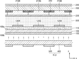
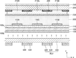
도 1을 참조하면, 본 실시예에 따른 액정 디스플레이 장치는 기판(100), 복수개의 화소전극들(120R, 120G, 120B), 차광층(220), 투광성 도광판(400) 및 광원부(500)를 구비한다.1, a liquid crystal display device according to an exemplary embodiment of the present invention includes a
기판(100)은 제1 면(100a)과 제1 면(100a)에 반대되는 제2 면(100b)을 가질 수 있다. 기판(100)은 투광성을 갖는 것으로서, 글라스재 기판일 수도 있고, 폴리이미드 등과 같은 고분자 물질을 포함하는 기판일 수도 있다. The
이러한 기판(100)의 제1 면(100a)에 복수개의 디스플레이 소자들이 배치된다. 디스플레이 소자들은 도시된 것과 같이 화소전극들(120R, 120G, 120B)과 공통전극(230) 사이에 액정(300)이 채워진 액정소자들일 수 있다. 화소전극들(120R, 120G, 120B)과 공통전극(230)도 투광성을 갖도록, ITO, IZO, ZnO 또는 In2O3 등의 투광성 물질을 포함할 수 있다. 화소전극들(120R, 120G, 120B)은 박막트랜지스터들이 전기적으로 연결될 수 있는바, 이를 위해 기판(100)과 화소전극들(120R, 120G, 120B) 사이에 박막트랜지스터층(110) 등이 개재될 수 있다.A plurality of display elements are disposed on the
물론 도 1에 도시된 것과 달리 화소전극들(120R, 120G, 120B)이나 공통전극(230) 상에는 배향막 등이 더 개재될 수 있는 등, 다양한 변형이 가능하다.Of course, unlike the one shown in FIG. 1, an orientation film and the like can be further provided on the
컬러필터들(210R, 210G, 210B)은 화소전극들(120R, 120G, 120B)이 사이에 위치되도록 기판(100)에 대향하여 배치될 수 있다. 컬러필터들(210R, 210G, 210B)은 각각 화소전극들(120R, 120G, 120B)에 대응하도록 위치할 수 있다. 즉, 적색컬러필터(210R)는 적색부화소의 화소전극(120R)에 대응하고, 녹색컬러필터(210G)는 녹색부화소의 화소전극(120G)에 대응하며, 청색컬러필터(210B)는 청색부화소의 화소전극(120B)에 대응하도록 위치할 수 있다. 이에 따라 디스플레이 소자들이 기판(100)과 컬러필터들(210R, 210G, 210B) 사이에 위치하게 된다. 이러한 컬러필터들(210R, 210G, 210B)은 봉지기판(200) 상에 위치할 수 있다.The
차광층(220)은 화소전극들(120R, 120G, 120B) 사이에 대응하도록 배치될 수 있다. 차광층(220)은 화소전극들(120R, 120G, 120B) 사이에 배치되어 각각의 부화소들을 구획할 수 있다. 이러한 차광층(220)은 블랙 매트릭스로 이해될 수 있으며, 예컨대 블랙 수지로 형성될 수 있다. 도 1을 참조하면, 차광층(220)은 봉지기판(200) 상에 위치하는 컬러필터들(210R, 210G, 210B) 사이에 배치될 수 있다. 즉 컬러필터들(210R, 210G, 210B)이 각각의 화소전극에 대응하도록 배치되고, 차광층(220)은 이러한 컬러필터들(210R, 210G, 210B) 사이에 위치하도록 패터닝될 수 있다. 차광층(220)이 화소전극들(120R, 120G, 120B) 사이에 대응하도록 배치됨에 따라 외광 반사를 줄여 콘트라스트비를 향상시킬 수 있다.The
한편, 본 실시예에 따른 액정 디스플레이 장치는 디스플레이 소자들에 빛을 조사할 수 있는 광원부(500) 및 광원부(500)에서 발광하는 빛을 디스플레이 소자들에 전달하는 도광판(400)을 더 구비할 수 있다. 이와 같은 도광판(400)과 광원부(500)는 백라이트 유닛(BLU)으로 이해될 수 있다. 이러한 백라이트 유닛(BLU)은 빛을 방출하여 이 빛이 디스플레이 소자들을 통과해 컬러필터들(210R, 210G, 210B)에 도달함으로써, 이 컬러필터들(210R, 210G, 210B)이 가시광선 중 특정 파장 대역의 광을 통과시키게 됨에 따라 풀컬러 이미지 디스플레이가 이루어지도록 할 수 있다.The liquid crystal display device according to the present exemplary embodiment may further include a
광원부(500)는 기판(100)의 제2 면에서 디스플레이 소자 측으로 빛을 조사하는 기능을 수행할 수 있다. 액정 디스플레이 소자는 유기발광 디스플레이 소자와는 달리 디스플레이 소자 스스로 발광할 수 없기 때문에 디스플레이 패널 측으로 빛을 조사하는 광원부(500)를 필요로 한다. 이러한 광원부(500)는 도광판(400)의 하면, 즉 기판(100)이 배치된 측의 반대측면에 배치될 수 있다. 도광판(400)의 하면에 배치되는 광원부(500)는 화소전극들(120R, 120G, 120B) 사이에 대응하도록 배치된 차광층(220)에 대응하도록 배치될 수 있다. 본 실시예의 액정 디스플레이 장치는 투명 액정 디스플레이 장치인 바, 이미지가 디스플레이되는 부화소들 사이의 차광층(220)에 대응하도록 광원부(500)를 배치해야 투명 디스플레이의 특성을 유지하며 이미지를 디스플레이 할 수 있다.The
본 실시예에 따르면 광원부(500)는 유기발광소자(OLED)를 포함할 수 있다. 상술한 것과 같이 유기발광소자(OLED)는 스스로 빛을 발광할 수 있어, 유기발광소자(OLED)가 발광한 빛에 의해 액정 디스플레이 장치에 화상이 표시될 수 있다. 상술한 것과 같이 유기발광소자(OLED)를 포함하는 광원부(500)는 차광층(220)에 대응하도록 배치할 수 있으므로, 부화소들 사이에 광원부(500)의 위치 및 개수를 원하는 대로 배치할 수 있어 디스플레이 소자들에 균일한 빛을 제공할 수 있다.According to the present embodiment, the
도광판(400)은 광원부(500)와 기판(100) 사이에 개재될 수 있다. 이러한 도광판(400)은 광원부(500)에서 발광하는 빛을 디스플레이 소자 측으로 전달하는 역할을 할 수 있다. 따라서 도광판(400) 후면에 배치된 광원부(500)의 빛이 도광판(400)을 통하여 디스플레이 소자 측으로 전달되어야 하므로, 도광판(400)은 투광성으로 형성될 수 있다. 또한 도광판(400)이 투광성이어야 사용자가 디스플레이 장치 후방, 구체적으로 백라이트 유닛(BLU)의 후방의 백그라운드를 인식할 수 있기 때문이다.The
한편, 기판(100)과 도광판(400) 사이에 개재되는 제1 편광판(150) 및 봉지기판(200) 상에 배치되는 제2 편광판(250)을 더 구비할 수 있다. 제1 편광판(150)은 기판(100)의 제2 면(100b)에 배치될 수 있다. 제1 편광판(150)은 기판(100)의 제2 면(100b) 전면(全面)에 배치될 수 있으며, 제2 편광판(250) 역시 봉지기판(200) 상면 전면(全面)에 배치될 수 있다. 이러한 편광판(150, 250)은 입사되는 광 중 소정의 방향(편광축 방향)의 성분만을 투과시키는 기능을 하므로, 광 흡수율이 높은 광학 소자일 수 있다.A
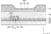
도 2는 도 1의 액정 디스플레이 장치의 광원부(500)를 개략적으로 도시하는 단면도이다. 2 is a cross-sectional view schematically showing the
상술한 것과 같이 본 실시예에 따른 광원부(500)는 유기발광소자(OLED)를 포함할 수 있다. 이러한 유기발광소자(OLED)는 투광성으로 형성될 수 있으나, 반드시 이에 한정되는 것은 아니다. 광원부(500)는 제1 전극(510), 제2 전극(530) 및 제1 전극(510)과 제2 전극(530) 사이에 개재되는 중간층(520)을 포함할 수 있다. 이하에서는 유기발광소자(OLED)를 포함하는 광원부(500)의 구조에 대하여 상세히 설명하도록 한다.As described above, the
도 2를 참조하면, 기판(501) 상에는 박막트랜지스터(TFT)가 배치될 수 있다. 박막트랜지스터(TFT)는 비정질실리콘, 다결정실리콘 또는 유기반도체물질을 포함하는 반도체층(502), 게이트전극(504), 소스전극(506s) 및 드레인전극(506d)을 포함한다. 이하 박막트랜지스터(TFT)의 일반적인 구성을 자세히 설명한다.Referring to FIG. 2, a thin film transistor (TFT) may be disposed on the
기판(501) 상에는 기판(501)의 면을 평탄화하기 위해 또는 반도체층(502)으로 불순물 등이 침투하는 것을 방지하기 위해, 실리콘옥사이드 또는 실리콘나이트라이드 등으로 형성된 버퍼층(503)이 배치되고, 이 버퍼층(503) 상에 반도체층(502)이 위치하도록 할 수 있다.A
반도체층(502)의 상부에는 게이트전극(504)이 배치되는데, 이 게이트전극(504)에 인가되는 신호에 따라 소스전극(506s) 및 드레인전극(506d)이 전기적으로 소통된다. 게이트전극(504)은 인접층과의 밀착성, 적층되는 층의 표면 평탄성 그리고 가공성 등을 고려하여, 예컨대 알루미늄(Al), 백금(Pt), 팔라듐(Pd), 은(Ag), 마그네슘(Mg), 금(Au), 니켈(Ni), 네오디뮴(Nd), 이리듐(Ir), 크롬(Cr), 리튬(Li), 칼슘(Ca), 몰리브덴(Mo), 티타늄(Ti), 텅스텐(W), 구리(Cu) 중 하나 이상의 물질로 단층 또는 다층으로 형성될 수 있다.A
이때 반도체층(502)과 게이트전극(504)과의 절연성을 확보하기 위하여, 실리콘옥사이드 및/또는 실리콘나이트라이드 등으로 형성되는 게이트절연막(505)이 반도체층(502)과 게이트전극(504) 사이에 개재될 수 있다.A
게이트전극(504)의 상부에는 층간절연막(507)이 배치될 수 있는데, 이는 실리콘옥사이드 또는 실리콘나이트라이드 등의 물질로 단층으로 형성되거나 또는 다층으로 형성될 수 있다.An interlayer insulating
층간절연막(507)의 상부에는 소스전극(506s) 및 드레인전극(506d)이 배치된다. 소스전극(506s) 및 드레인전극(506d)은 층간절연막(507)과 게이트절연막(505)에 형성되는 컨택홀을 통하여 반도체층(502)에 각각 전기적으로 연결된다. 소스전극(506s) 및 드레인전극(506d)은 도전성 등을 고려하여 예컨대 알루미늄(Al), 백금(Pt), 팔라듐(Pd), 은(Ag), 마그네슘(Mg), 금(Au), 니켈(Ni), 네오디뮴(Nd), 이리듐(Ir), 크롬(Cr), 리튬(Li), 칼슘(Ca), 몰리브덴(Mo), 티타늄(Ti), 텅스텐(W), 구리(Cu) 중 하나 이상의 물질로 단층 또는 다층으로 형성될 수 있다.A
이러한 구조의 박막트랜지스터(TFT)의 보호를 위해 도 2에는 도시되어 있지않으나, 박막트랜지스터(TFT)를 덮는 보호막(미도시)이 더 배치될 수 있다. 보호막은 예컨대 실리콘옥사이드, 실리콘나이트라이드 또는 실리콘옥시나이트라이드 등과 같은 무기물로 형성될 수 있다. 이러한 보호막은 단층 또는 다층구조를 가질 수도 있는 등 다양한 변형이 가능하다.Though not shown in FIG. 2 for the protection of the thin film transistor (TFT) having such a structure, a protective film (not shown) covering the thin film transistor TFT may be further disposed. The protective film may be formed of an inorganic material such as silicon oxide, silicon nitride or silicon oxynitride. Such a protective film may have a single layer or a multilayer structure, and various modifications are possible.
한편, 기판(501)의 상에 평탄화막(509)이 배치될 수 있다. 이 경우 평탄화막(509)은 말 그대로 유기발광소자(OLED)가 배치되는 박막트랜지스터 상부를 평탄화 시키기 위한 평탄화막일 수도 있고, 박막트랜지스터가 위치한 하부를 보호하기 위한 보호막일 수도 있다. 이러한 보호막(미도시)과 평탄화막(509)은 예컨대 아크릴계 유기물 또는 BCB(Benzocyclobutene) 등으로 형성될 수 있다. 이때 도 3에 도시된 것과 같이, 게이트절연막(505), 층간절연막(507), 보호막(미도시), 평탄화막(509)은 기판(501)의 전면(全面)에 형성될 수 있다.On the other hand, the
한편, 박막트랜지스터(TFT) 상부에는 화소정의막(512)이 배치될 수 있다. 화소정의막(512)은 상술한 평탄화막(509) 상에 위치할 수 있으며, 제1 전극(510)의 중앙부를 노출시키는 개구를 가질 수 있다. 이러한 화소정의막(512)은 제1 전극(510)의 중앙부를 노출시키도록 패터닝 됨에 따라 기판(501) 상에 화소영역을 정의하는 역할을 한다.On the other hand, a
이러한 화소정의막(512)은 예컨대 유기물로 형성될 수 있다. 그러한 유기물로는 예컨대, 폴리메틸메타크릴레이트(PMMA)와 같은 아크릴계 고분자, 폴리스티렌(PS), phenol그룹을 갖는 고분자 유도체, 이미드계 고분자, 아릴에테르계 고분자, 아마이드계 고분자, 불소계고분자, p-자일렌계 고분자, 비닐알콜계 고분자 및 이들의 혼합물 등을 포함할 수 있다.The
한편 도 2에 도시된 것과 같이, 평탄화막(509) 상에는 유기발광소자(OLED)가 배치될 수 있다. 이러한 유기발광소자(OLED)는 제1 전극(510), 제1 전극(510) 상에 배치되는 발광층을 포함한 중간층(520) 및 중간층(520)을 덮도록 배치되는 제2 전극(530)을 포함할 수 있다. 이 경우 중간층(520)은 백색광을 발광할 수 있다.On the other hand, as shown in FIG. 2, the organic light emitting device OLED may be disposed on the
제1 전극(510)은 평탄화막(509) 상에 배치될 수 있다. 이 경우 평탄화막(509)에는 박막트랜지스터(TFT)의 소스전극(506s) 및 드레인전극(506d) 중 적어도 어느 하나를 노출시키는 개구부가 존재하며, 이 개구부를 통해 제1 전극(510)은 박막트랜지스터(TFT)의 소스전극(506s) 및 드레인전극(506d) 중 어느 하나와 컨택하여 박막트랜지스터(TFT)와 전기적으로 연결될 수 있다.The
제1 전극(510) 은 (반)투명 전극 또는 반사형 전극으로 형성될 수 있다. (반)투명 전극으로 형성될 때에는 예컨대 ITO, IZO, ZnO, In2O3, IGO 또는 AZO로 형성될 수 있다. 반사형 전극으로 형성될 때에는 Ag, Mg, Al, Pt, Pd, Au, Ni, Nd, Ir, Cr 및 이들의 화합물 등으로 형성된 반사막과, ITO, IZO, ZnO, In2O3, IGO 또는 AZO로 형성된 층을 가질 수 있다. 물론 본 발명이 이에 한정되는 것은 아니고 다양한 재질로 형성될 수 있으며, 그 구조 또한 단층 또는 다층이 될 수 있는 등 다양한 변형이 가능하다.The
화소정의막(512)에 의해 정의된 화소영역에는 발광층을 포함하는 중간층(520)이 배치될 수 있다. 유기발광소자(OLED)의 중간층(520)은 발광층(EML: Emission Layer)을 포함하며, 발광층을 이외에 홀 주입층(HIL: Hole Injection Layer), 홀 수송층(HTL: Hole Transport Layer), 전자 수송층(ETL: Electron Transport Layer), 전자 주입층(EIL: Electron Injection Layer) 등이 단일 혹은 복합의 구조로 적층되어 형성될 수 있다. 물론 중간층(520)은 반드시 이에 한정되는 것은 아니고, 다양한 구조를 가질 수도 있음은 물론이다.An
중간층(520)은 저분자 유기물 또는 고분자 유기물일 수 있다. 중간층(520)은 홀 수송층(hole transport layer: HTL), 홀 주입층(hole injection layer: HIL), 전자 수송층(electron transport layer: ETL) 및 전자 주입층(electron injection layer: EIL) 등이 선택적으로 적층될 수 있으며, 상기 다층구조 사이에 발광층(EML)이 개재될 수 있다. 이외에도 필요에 따라 다양한 층들이 적층 될 수 있다. 이때 홀 수송층(HTL), 홀 주입층(HIL), 전자 수송층(ETL) 및 전자 주입층(EIL)은 기판(501) 전면(全面)에 일체(一體)로 형성될 수 있고, 발광층(EML)만 잉크젯 프린팅 공정으로 화소별로 형성될 수 있다.The
본 실시예에 따른 중간층(520)은 백색광을 발광할 수 있다. 중간층(520)은 발광층(EML)을 포함하는데, 이러한 발광층(EML)은 일반적으로 적색(R), 녹색(G), 청색(B) 중 한가지 색을 발광할 수 있다. 중간층(520)이 백색광을 발광하는 방법은 특정한 방법에 한정되지 않으며, 예컨대 적색 발광층, 녹색 발광층, 청색 발광층을 다층구조로 배치하거나, 적색을 발광하는 유기발광소자(OLED), 녹색을 발광하는 유기발광소자(OLED) 및 청색을 발광하는 유기발광소자(OLED)를 적절히 조합하여 형성할 수 있다.The
발광층을 포함하는 중간층(520)을 덮으며 제1 전극(510)에 대향하는 제2 전극(530)이 기판(501) 전면(全面)에 걸쳐서 배치될 수 있다. 제2 전극(530)은 (반)투명 전극 또는 반사형 전극으로 형성될 수 있다. The
제2 전극(530)이 (반)투명 전극으로 형성될 때에는 일함수가 작은 금속 즉, Li, Ca, LiF/Ca, LiF/Al, Al, Ag, Mg 및 이들의 화합물로 형성된 층과 ITO, IZO, ZnO 또는 In2O3 등의 (반)투명 도전층을 가질 수 있다. 제2 전극(530)이 반사형 전극으로 형성될 때에는 Li, Ca, LiF/Ca, LiF/Al, Al, Ag, Mg 및 이들의 화합물로 형성된 층을 가질 수 있다. 물론 제2 전극(530)의 구성 및 재료가 이에 한정되는 것은 아니며 다양한 변형이 가능함은 물론이다.The
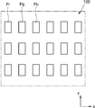
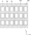
도 3은 도 1의 액정 디스플레이 장치를 개략적으로 도시하는 평면도이고, 도 4는 도 3의 액정 디스플레이 장치의 도광판(400)과 광원부(500)를 개략적으로 도시하는 저면도이며, 도 5는 본 발명의 다른 일 실시예에 관한 액정 디스플레이 장치의 도광판(400)과 광원부(500)를 개략적으로 도시하는 저면도이다.FIG. 3 is a plan view schematically illustrating the liquid crystal display device of FIG. 1, FIG. 4 is a bottom view schematically showing the
도 3 및 도 5를 참조하면, 각각의 부화소들(Pr, Pg, Pb)은 서로 이격되어 배치될 수 있다. 부화소들(Pr, Pg, Pb)은 서로 다른 색의 광을 방출하는 제1 부화소(Pr), 제2 부화소(Pg) 및 제3 부화소(Pb)를 포함할 수 있다. 제1 부화소는 적색광을 방출하고, 제2 부화소는 녹색광을 방출하며, 제3 부화소는 청색광을 방출할 수 있으나, 본 발명이 반드시 이에 한정되는 것은 아니다. 상기 색상은 부화소들(Pr, Pg, Pb) 각각에 대응되도록 배치된 컬러필터들(210R, 210G, 210B) 또는 색변환층(color conversion layer)(미도시)에 의해 부여될 수 있으며, 부화소들(Pr, Pg, Pb) 각각은 차광층(220)에 의해 구획될 수 있다.Referring to FIGS. 3 and 5, each of the sub-pixels Pr, Pg, and Pb may be spaced apart from each other. The sub-pixels Pr, Pg, and Pb may include a first sub-pixel Pr, a second sub-pixel Pg, and a third sub-pixel Pb that emit light of different colors. The first sub-pixel emits red light, the second sub-pixel emits green light, and the third sub-pixel emits blue light, but the present invention is not necessarily limited thereto. The hue may be imparted by
본 실시예에 따른 광원부(500)는 도 4에 도시된 것과 같이, 부화소들(Pr, Pg, Pb) 사이에 배치될 수 있으며, 차광층(220)과 대응되는 위치에 메쉬(mesh) 형태로 패터닝될 수 있다. 부화소들(Pr, Pg, Pb)은 차광층(220)에 의해 구획되고, 상술한 것과 같이 유기발광소자(OLED)를 포함하는 광원부(500)는 차광층(220)에 대응하도록 배치할 수 있다. 따라서 부화소들(Pr, Pg, Pb) 사이에 광원부(500)의 위치 및 개수를 원하는 대로 배치할 수 있어 각각의 부화소들(Pr, Pg, Pb)에 균일한 빛을 제공할 수 있다.4, the
도 5를 참조하면, 광원부(500)는 부화소들(Pr, Pg, Pb) 사이에 배치될 수 있으며, 차광층(220)과 대응되는 위치에 아일랜드(island) 형태로 패터닝될 수 있다. 도 5에는 도시되어 있지 않으나 아일랜드 형태로 부화소들(Pr, Pg, Pb) 사이에 이격되어 배치된 광원부(500)를 연결하는 배선 등이 더 형성될 수도 있다. 상술한 실시예 이외에도 광원부(500)의 배치 형태는 다양한 형태를 가질 수 있다.5, the
한편 도 1, 도 4 및 도 5에 도시된 것과 같이, 부화소들(Pr, Pg, Pb) 각각은 차광층(220)에 의해 구획될 수 있고 즉 부화소들(Pr, Pg, Pb) 사이에 대응되는 위치에 차광층(220)이 배치될 수 있다. 광원부(500)는 이러한 차광층(220)과 대응되는 위치에 메쉬 형태 또는 아일랜드 형태로 패터닝될 수 있다. 이러한 광원부(500)는 차광층(220)의 면적보다 작거나 동일한 면적을 가질 수 있다. 본 실시예의 액정 디스플레이 장치는 시-쓰루 액정 디스플레이 장치인 바, 이미지가 디스플레이되는 부화소들(Pr, Pg, Pb) 사이의 차광층(220)이 배치된 면적과 동일하거나 그 보다 적은 면적에 대응하도록 광원부(500)를 배치해야 투명 디스플레이의 특성을 유지하며 이미지를 디스플레이 할 수 있기 때문이다.As shown in FIGS. 1, 4 and 5, each of the sub-pixels Pr, Pg and Pb may be partitioned by the
도 6은 본 발명의 또 다른 일 실시예에 관한 액정 디스플레이 장치를 개략적으로 도시하는 단면도이다.6 is a cross-sectional view schematically showing a liquid crystal display device according to another embodiment of the present invention.
도 6을 참조하면, 본 실시예에 따른 액정 디스플레이 장치는 백라이트 유닛(BLU)에 있어서 변형된 구조를 갖는다. 본 실시예에 따른 액정 디스플레이 장치는 기판(100), 복수개의 화소전극들(120R, 120G, 120B), 차광층(220) 및 도광판(400), 광원부(500), 도광판(400)과 광원부(500) 사이에 개재되는 편광판(550)을 포함하는 백라이트 유닛(BLU)을 구비한다.Referring to FIG. 6, the liquid crystal display device according to the present embodiment has a modified structure in a backlight unit (BLU). The liquid crystal display device according to the present embodiment includes a
기판(100)은 제1 면(100a)과 제1 면(100a)에 반대되는 제2 면(100b)을 가질 수 있다. 기판(100)은 투광성을 갖는 것으로서, 글라스재 기판일 수도 있고, 폴리이미드 등과 같은 고분자 물질을 포함하는 기판일 수도 있다.The
이러한 기판(100)의 제1 면(100a)에 복수개의 디스플레이 소자들이 배치된다. 디스플레이 소자들은 도시된 것과 같이 화소전극들(120R, 120G, 120B)과 공통전극(230) 사이에 액정(300)이 채워진 액정소자들일 수 있다. 화소전극들(120R, 120G, 120B)과 공통전극(230)도 투광성을 갖도록, ITO, IZO, ZnO 또는 In2O3 등의 투광성 물질을 포함할 수 있다. 화소전극들(120R, 120G, 120B)은 박막트랜지스터들이 전기적으로 연결될 수 있는바, 이를 위해 기판(100)과 화소전극들(120R, 120G, 120B) 사이에 박막트랜지스터층(110) 등이 개재될 수 있다.A plurality of display elements are disposed on the
물론 도 6에 도시된 것과 달리 화소전극들(120R, 120G, 120B)이나 공통전극(230) 상에는 배향막 등이 더 개재될 수 있는 등, 다양한 변형이 가능하다.Of course, unlike the structure shown in FIG. 6, an orientation film or the like may be further provided on the
컬리필터들은 화소전극들(120R, 120G, 120B)이 사이에 위치되도록 기판(100)에 대향하여 배치될 수 있다. 컬러필터들(210R, 210G, 210B)은 각각 화소전극들(120R, 120G, 120B)에 대응하도록 위치할 수 있다. 즉, 적색컬러필터(210R)는 적색부화소의 화소전극(120R)에 대응하고, 녹색컬러필터(210G)는 녹색부화소의 화소전극(120G)에 대응하며, 청색컬러필터(210B)는 청색부화소의 화소전극(120B)에 대응하도록 위치할 수 있다. 이에 따라 디스플레이 소자들이 기판(100)과 컬러필터들(210R, 210G, 210B) 사이에 위치하게 된다. 이러한 컬러필터들(210R, 210G, 210B)은 봉지기판(200) 상에 위치할 수 있다.The collinear filters may be disposed to face the
차광층(220)은 화소전극들(120R, 120G, 120B) 사이에 대응하도록 배치될 수 있다. 차광층(220)은 화소전극들(120R, 120G, 120B) 사이에 배치되어 각각의 부화소들을 구획할 수 있다. 이러한 차광층(220)은 블랙 매트릭스로 이해될 수 있으며, 예컨대 블랙 수지로 형성될 수 있다. 도 6을 참조하면, 차광층(220)은 봉지기판(200) 상에 위치하는 컬러필터들(210R, 210G, 210B) 사이에 배치될 수 있다. 즉 컬러필터들(210R, 210G, 210B)이 각각의 화소전극에 대응하도록 배치되고, 차광층(220)은 이러한 컬러필터들(210R, 210G, 210B) 사이에 위치하도록 패터닝될 수 있다. 차광층(220)이 화소전극들(120R, 120G, 120B) 사이에 대응하도록 배치됨에 따라 외광 반사를 줄여 콘트라스트비를 향상시킬 수 있다.The
한편, 본 실시예에 따른 액정 디스플레이 장치는 디스플레이 소자들에 빛을 조사할 수 있는 광원부(500) 및 광원부(500)에서 발광하는 빛을 디스플레이 소자들에 전달하는 도광판(400)을 더 구비할 수 있다. 이와 같은 도광판(400)과 광원부(500)는 백라이트 유닛(BLU)으로 이해될 수 있다. 이러한 백라이트 유닛(BLU)은 빛을 방출하여 이 빛이 디스플레이 소자들을 통과해 컬러필터들(210R, 210G, 210B)에 도달함으로써, 이 컬러필터들(210R, 210G, 210B)이 가시광선 중 특정 파장 대역의 광을 통과시키게 됨에 따라 풀컬러 이미지 디스플레이가 이루어지도록 할 수 있다.The liquid crystal display device according to the present exemplary embodiment may further include a
광원부(500)는 기판(100)의 제2 면(100b)에서 디스플레이 소자 측으로 빛을 조사하는 기능을 수행할 수 있다. 액정 디스플레이 소자는 유기발광 디스플레이 소자와는 달리 디스플레이 소자 스스로 발광할 수 없기 때문에 기판(100)의 후면부에 빛을 조사하는 광원부(500)를 필요로 한다. 이러한 광원부(500)는 도광판(400)의 후면에 배치될 수 있다. 도광판(400)의 후면에 배치되는 광원부(500)는 부화소들 사이에 대응하도록 배치된 차광층(220)에 대응하도록 배치될 수 있다. 본 실시예의 액정 디스플레이 장치는 시-쓰루 액정 디스플레이 장치인 바, 이미지가 디스플레이되는 부화소들 사이의 차광층(220)에 대응하도록 광원부(500)를 배치해야 투명 디스플레이의 특성을 유지하며 이미지를 디스플레이 할 수 있다.The
본 실시예에 따르면 광원부(500)는 유기발광소자(OLED)를 포함할 수 있다. 상술한 것과 같이 유기발광소자(OLED)는 스스로 빛을 발광할 수 있어, 유기발광소자(OLED)가 발광한 빛에 의해 액정 디스플레이 장치에 화상이 표시될 수 있다. 상술한 것과 같이 유기발광소자(OLED)를 포함하는 광원부(500)는 차광층(220)에 대응하도록 배치할 수 있으므로, 부화소들 사이에 광원부(500)의 위치 및 개수를 원하는 대로 배치할 수 있어 디스플레이 소자들에 균일한 빛을 제공할 수 있다.According to the present embodiment, the
도광판(400)은 광원부(500)와 기판(100) 사이에 개재될 수 있다. 이러한 도광판(400)은 광원부(500)에서 발광하는 빛을 디스플레이 소자 측으로 전달하는 역할을 할 수 있다. 따라서 도광판(400) 후면에 배치된 광원부(500)의 빛이 도광판(400)을 통하여 디스플레이 소자 측으로 전달되어야 하므로, 도광판(400)은 투광성으로 형성될 수 있다. 또한 도광판(400)이 투광성이어야 사용자가 디스플레이 장치 후방, 구체적으로 백라이트 유닛(BLU)의 후방의 백그라운드를 인식할 수 있기 때문이다.The
한편, 도광판(400)과 광원부(500) 사이에 개재되는 제1 편광판(550)을 더 구비할 수 있다. 또한 봉지기판(200) 상에 배치되는 제2 편광판(250)을 더 구비할 수 있다. 제1 편광판(550)은 기판(100)의 제2 면에 배치될 수 있다. 제1 편광판(550)은 기판(100)의 제2 면 전면(全面)에 배치될 수 있으며, 제2 편광판(250) 역시 봉지기판(200) 상면 전면(全面)에 배치될 수 있다. 이러한 편광판(150, 250)은 입사되는 광 중 소정의 방향(편광축 방향)의 성분만을 투과시키는 기능을 하므로, 광 흡수율이 높은 광학 소자일 수 있다.The
제1 편광판(550)은 광원부(500)에 대응하도록 패터닝될 수 있다. 즉 도 4 및 도 5를 참조하여 전술한 것과 같이 광원부(500)가 차광층(220)과 대응되는 위치에 메쉬 형태 또는 아일랜드 형태로 다양한 형태를 갖도록 패터닝될 수 있고, 제1 편광판(550)은 이러한 광원부(500)에 대응하도록 패터닝될 수 있다. 이 경우 패널의 투과율을 높이기 위해, 제1 편광판(550)은 와이어 그리드 편광판(WGP; wire-grid polarizer)일 수 있다. 와이어 그리드 편광판은, 평행하게 배치되어 있는 미세 금속 와이어들의 규칙적인 어레이로 구성될 수 있다. 와이어 그리드 편광판은, 통상의 편광자와 동일한 기능을 수행하지만 편광판을 구성하는 물질을 연신(orientation)시키지 않고 금속 와이어를 입사되는 광의 파장 이하의 간격으로 배치한 것으로써, 패터닝이 용이하다는 장점을 가질 수 있다. 따라서 제1 편광판(550)을 와이어 그리드 편광판으로 형성하여 광원부(500)에 대응하는 위치에만 배치함으로써 디스플레이 패널의 투과율을 획기적으로 향상시킬 수 있다.The first
본 발명은 도면에 도시된 실시예를 참고로 설명되었으나 이는 예시적인 것에 불과하며, 당해 기술분야에서 통상의 지식을 가진 자라면 이로부터 다양한 변형 및 균등한 다른 실시예가 가능하다는 점을 이해할 것이다. 따라서 본 발명의 진정한 기술적 보호 범위는 첨부된 특허청구범위의 기술적 사상에 의하여 정해져야 할 것 이다. While the present invention has been described with reference to exemplary embodiments, it is to be understood that the invention is not limited to the disclosed exemplary embodiments, but, on the contrary, is intended to cover various modifications and equivalent arrangements included within the spirit and scope of the invention. Therefore, the true scope of the present invention should be determined by the technical idea of the appended claims.
100: 기판
110: 박막트랜지스터층
120G, 120R, 120B: 화소전극들
200: 봉지기판
210R, 210G, 210B: 컬러필터들
220: 차광층
230: 공통전극
300: 액정
400: 도광판
500: 광원부
550: 편광판100: substrate
110: thin film transistor layer
120G, 120R, and 120B:
200: sealing substrate
210R, 210G, 210B: Color filters
220: Shading layer
230: common electrode
300: liquid crystal
400: light guide plate
500: light source part
550: polarizer
Claims (11)
상기 기판의 제1 면에 배치된 복수개의 화소전극들;
상기 복수개의 화소전극들 사이에 대응하도록 배치된 차광층;
상기 차광층에 대응하며 상기 기판의 제2 면에 빛을 조사하는 광원부; 및
상기 광원부와 상기 기판 사이에 개재되는 투광성 도광판;
를 구비하는, 액정 디스플레이 장치.A substrate having a first side and a second side opposite to the first side;
A plurality of pixel electrodes disposed on a first surface of the substrate;
A light-shielding layer disposed so as to correspond to the plurality of pixel electrodes;
A light source unit corresponding to the light-shielding layer and irradiating light to the second surface of the substrate; And
A translucent light guide plate interposed between the light source and the substrate;
And the liquid crystal display device.
상기 광원부는 유기발광소자를 포함하는, 액정 디스플레이 장치.The method according to claim 1,
Wherein the light source portion includes an organic light emitting element.
상기 유기발광소자는, 제1 전극과, 제2 전극과, 상기 제1 전극 및 상기 제2 전극 사이에 개재되며 백색광을 발광하는 중간층을 포함하는, 액정 디스플레이 장치.3. The method of claim 2,
Wherein the organic light emitting element includes a first electrode, a second electrode, and an intermediate layer interposed between the first electrode and the second electrode and emitting white light.
상기 복수개의 화소전극들이 사이에 위치되도록 상기 기판에 대향하여 배치된 컬러필터들을 더 구비하며,
상기 차광층은 상기 컬러필터들 사이에 배치되는, 액정 디스플레이 장치.The method according to claim 1,
Further comprising color filters disposed opposite the substrate such that the plurality of pixel electrodes are located between the color filters,
And the light shielding layer is disposed between the color filters.
상기 광원부는 상기 차광층의 면적보다 작거나 동일한 면적을 갖는, 액정 디스플레이 장치.5. The method of claim 4,
And the light source portion has an area smaller than or equal to the area of the light shielding layer.
상기 광원부는 상기 차광층과 대응되는 위치에 메쉬(mesh) 형태로 배치되는, 액정 디스플레이 장치.5. The method of claim 4,
Wherein the light source unit is disposed in a mesh shape at a position corresponding to the light shielding layer.
상기 광원부는 상기 차광층과 대응되는 위치에 아일랜드(island) 형태로 배치되는, 액정 디스플레이 장치5. The method of claim 4,
Wherein the light source unit is disposed in an island shape at a position corresponding to the light shielding layer,
상기 기판과 상기 도광판 사이에 개재되는 편광판을 더 구비하는, 액정 디스플레이 장치.The method according to claim 1,
And a polarizing plate interposed between the substrate and the light guide plate.
상기 도광판과 상기 광원부 사이에 개재되는 편광판을 더 구비하며, 상기 편광판은 상기 광원부에 대응하도록 패터닝된, 액정 디스플레이 장치.The method according to claim 1,
And a polarizing plate interposed between the light guide plate and the light source unit, wherein the polarizing plate is patterned to correspond to the light source unit.
상기 편광판은 와이어 그리드 편광판(WGP; wire-grid polarizer)인, 액정 디스플레이 장치.10. The method of claim 9,
Wherein the polarizing plate is a wire-grid polarizer (WGP).
상기 도광판 및 상기 광원부는 플렉서블한 특성을 갖는, 액정 디스플레이 장치.
The method according to claim 1,
Wherein the light guide plate and the light source unit have flexible characteristics.
Priority Applications (2)
| Application Number | Priority Date | Filing Date | Title |
|---|---|---|---|
| KR1020150000292A KR20160084005A (en) | 2015-01-02 | 2015-01-02 | Liquid crystal display apparatus |
| US14/973,607 US20160195760A1 (en) | 2015-01-02 | 2015-12-17 | Liquid crystal display apparatus |
Applications Claiming Priority (1)
| Application Number | Priority Date | Filing Date | Title |
|---|---|---|---|
| KR1020150000292A KR20160084005A (en) | 2015-01-02 | 2015-01-02 | Liquid crystal display apparatus |
Publications (1)
| Publication Number | Publication Date |
|---|---|
| KR20160084005A true KR20160084005A (en) | 2016-07-13 |
Family
ID=56286423
Family Applications (1)
| Application Number | Title | Priority Date | Filing Date |
|---|---|---|---|
| KR1020150000292A KR20160084005A (en) | 2015-01-02 | 2015-01-02 | Liquid crystal display apparatus |
Country Status (2)
| Country | Link |
|---|---|
| US (1) | US20160195760A1 (en) |
| KR (1) | KR20160084005A (en) |
Families Citing this family (5)
| Publication number | Priority date | Publication date | Assignee | Title |
|---|---|---|---|---|
| TWI549330B (en) * | 2014-06-04 | 2016-09-11 | 群創光電股份有限公司 | Organic light emitting diode display |
| CN106597599A (en) * | 2017-01-17 | 2017-04-26 | 京东方科技集团股份有限公司 | Backlight module, display panel and display device |
| CN109991775B (en) * | 2018-01-03 | 2020-06-30 | 京东方科技集团股份有限公司 | Backlight and display device |
| JP7065798B2 (en) * | 2019-02-13 | 2022-05-12 | 三菱電機株式会社 | Display devices and automobiles |
| US20220399410A1 (en) * | 2021-02-25 | 2022-12-15 | Chengdu Boe Optoelectronics Technology Co., Ltd. | Display device and manufacturing method thereof |
Family Cites Families (5)
| Publication number | Priority date | Publication date | Assignee | Title |
|---|---|---|---|---|
| JP3487782B2 (en) * | 1999-03-17 | 2004-01-19 | 株式会社日立製作所 | Liquid crystal display |
| JP2007273091A (en) * | 2006-03-30 | 2007-10-18 | Fujitsu Ltd | Prism light guide plate, lighting device, and electronic device |
| KR102144993B1 (en) * | 2013-10-02 | 2020-08-14 | 삼성전자주식회사 | Display device |
| US9651825B2 (en) * | 2014-09-23 | 2017-05-16 | Au Optronics Corporation | Liquid crystal lens display device with light shield structure |
| KR20160147172A (en) * | 2015-06-12 | 2016-12-22 | 삼성디스플레이 주식회사 | Liquid crystal display and manufacturing method thereof |
-
2015
- 2015-01-02 KR KR1020150000292A patent/KR20160084005A/en not_active Application Discontinuation
- 2015-12-17 US US14/973,607 patent/US20160195760A1/en not_active Abandoned
Also Published As
| Publication number | Publication date |
|---|---|
| US20160195760A1 (en) | 2016-07-07 |
Similar Documents
| Publication | Publication Date | Title |
|---|---|---|
| CN107230687B (en) | Display device | |
| KR101338250B1 (en) | Display device | |
| US9786721B1 (en) | OLED display panel | |
| KR102146070B1 (en) | Organic Light Emitting Display | |
| KR102491876B1 (en) | Display apparutus | |
| KR102441558B1 (en) | Organic light-emitting display apparatus and method for manufacturing the same | |
| US20220376209A1 (en) | Display substrate and preparation method therefor, and display apparatus | |
| KR102354969B1 (en) | Organic light emitting display apparatus | |
| KR20160061540A (en) | Organic light emitting display device and method of manufacturing the same | |
| JP2017016822A (en) | Organic el device, method for manufacturing organic el device, and electronic apparatus | |
| KR20180009827A (en) | Display appartus | |
| KR20160084005A (en) | Liquid crystal display apparatus | |
| KR20160039080A (en) | Organic light-emitting display apparatus | |
| KR20160147093A (en) | Display device and method of manufacturing the same | |
| KR20170031847A (en) | Organic light-emitting display apparatus | |
| KR20210103037A (en) | display device and electric apparatus | |
| KR20160039745A (en) | Organic light-emitting display apparatus | |
| US20210359047A1 (en) | Display apparatus and method of manufacturing the same | |
| CN112018150B (en) | Display device | |
| KR101957145B1 (en) | Organic Light Emitting diode display and method of manufacturing the same | |
| KR20220001800A (en) | Display device | |
| KR20220027350A (en) | Display device | |
| US9685486B2 (en) | Organic light-emitting diode display with color filter layer | |
| KR20210036456A (en) | Display panel and display apparatus comprising the same | |
| CN114300509A (en) | Display panel and display device |
Legal Events
| Date | Code | Title | Description |
|---|---|---|---|
| WITN | Application deemed withdrawn, e.g. because no request for examination was filed or no examination fee was paid |