JP6552201B2 - Organic light emitting device - Google Patents
Organic light emitting device Download PDFInfo
- Publication number
- JP6552201B2 JP6552201B2 JP2015007532A JP2015007532A JP6552201B2 JP 6552201 B2 JP6552201 B2 JP 6552201B2 JP 2015007532 A JP2015007532 A JP 2015007532A JP 2015007532 A JP2015007532 A JP 2015007532A JP 6552201 B2 JP6552201 B2 JP 6552201B2
- Authority
- JP
- Japan
- Prior art keywords
- group
- organic
- light emitting
- layer
- organic light
- Prior art date
- Legal status (The legal status is an assumption and is not a legal conclusion. Google has not performed a legal analysis and makes no representation as to the accuracy of the status listed.)
- Active
Links
- 0 Cc1c(*)c(*)c(C(C2c3c(*)c(*)c(*)c(*)c3N(*)c3c2c(C)c(*)c(O*)c3*)c(c(*)c(*)c(*)c2[Re])c2N2*)c2c1* Chemical compound Cc1c(*)c(*)c(C(C2c3c(*)c(*)c(*)c(*)c3N(*)c3c2c(C)c(*)c(O*)c3*)c(c(*)c(*)c(*)c2[Re])c2N2*)c2c1* 0.000 description 14
- NRNSOYPFGYOIFC-KXFIGUGUSA-N C/C=C\c(ccc(cc1)c2nc1-c1cc(-c3cccc(-c4nc5c6NCC=Cc6ccc5cc4)c3)ccc1)c2N Chemical compound C/C=C\c(ccc(cc1)c2nc1-c1cc(-c3cccc(-c4nc5c6NCC=Cc6ccc5cc4)c3)ccc1)c2N NRNSOYPFGYOIFC-KXFIGUGUSA-N 0.000 description 1
- OEZLUMPYXVQFGT-UHFFFAOYSA-N CC(C)(C)c(cc1)ccc1N(c1c2cccc1)c1ccccc1C2=C1c2ccccc2N(c2ccc(C(C)(C)C)cc2)c2c1cccc2 Chemical compound CC(C)(C)c(cc1)ccc1N(c1c2cccc1)c1ccccc1C2=C1c2ccccc2N(c2ccc(C(C)(C)C)cc2)c2c1cccc2 OEZLUMPYXVQFGT-UHFFFAOYSA-N 0.000 description 1
- ROFNOEJYTANKRU-VGFSZAGXSA-N CC(C)(C)c(cc1N(c2ccccc2)c2c3cccc2)ccc1/C3=C1/c2ccc(C(C)(C)C)cc2N(c2ccccc2)c2ccccc12 Chemical compound CC(C)(C)c(cc1N(c2ccccc2)c2c3cccc2)ccc1/C3=C1/c2ccc(C(C)(C)C)cc2N(c2ccccc2)c2ccccc12 ROFNOEJYTANKRU-VGFSZAGXSA-N 0.000 description 1
- UIOMGHGKKLWNJK-UHFFFAOYSA-N CC1(C)c(cc(cc2)-c(cc3)cc(C(c4c5)=O)c3Sc4ccc5-c(cc3C4(C)C)ccc3-c3c4cccc3)c2-c2c1cccc2 Chemical compound CC1(C)c(cc(cc2)-c(cc3)cc(C(c4c5)=O)c3Sc4ccc5-c(cc3C4(C)C)ccc3-c3c4cccc3)c2-c2c1cccc2 UIOMGHGKKLWNJK-UHFFFAOYSA-N 0.000 description 1
- JWKNYFLLVWKHMR-DBFBYELTSA-N CC1(C)c(ccc(N(c2ccccc2/C(/c2c3)=C4\c(cc(cc5)F)c5N(c5ccc(C(C)(C)c6ccccc6-6)c-6c5)c5ccccc45)c2ccc3F)c2)c2-c2c1cccc2 Chemical compound CC1(C)c(ccc(N(c2ccccc2/C(/c2c3)=C4\c(cc(cc5)F)c5N(c5ccc(C(C)(C)c6ccccc6-6)c-6c5)c5ccccc45)c2ccc3F)c2)c2-c2c1cccc2 JWKNYFLLVWKHMR-DBFBYELTSA-N 0.000 description 1
- SOXPWTOOZZFQOG-UHFFFAOYSA-N Cc(cc1)ccc1N(c1c2cccc1)c1ccccc1C2=C1c2ccccc2N(c2ccc(C)cc2)c2c1cccc2 Chemical compound Cc(cc1)ccc1N(c1c2cccc1)c1ccccc1C2=C1c2ccccc2N(c2ccc(C)cc2)c2c1cccc2 SOXPWTOOZZFQOG-UHFFFAOYSA-N 0.000 description 1
- DEBAJVYIBRJWSG-UHFFFAOYSA-N Cc(cc1N(c2cc(F)cc(F)c2)c2c3ccc(C)c2)ccc1C3=C1c2ccc(C)cc2N(c2cc(F)cc(F)c2)c2c1ccc(C)c2 Chemical compound Cc(cc1N(c2cc(F)cc(F)c2)c2c3ccc(C)c2)ccc1C3=C1c2ccc(C)cc2N(c2cc(F)cc(F)c2)c2c1ccc(C)c2 DEBAJVYIBRJWSG-UHFFFAOYSA-N 0.000 description 1
- RIQXUPWGMPFUEH-WQVHNPAPSA-N Cc1cc(N(c2c3cccc2)c2cc(F)ccc2/C3=C2/c(ccc(F)c3)c3N(c3cc(C)cc(C)c3)c3ccccc23)cc(C)c1 Chemical compound Cc1cc(N(c2c3cccc2)c2cc(F)ccc2/C3=C2/c(ccc(F)c3)c3N(c3cc(C)cc(C)c3)c3ccccc23)cc(C)c1 RIQXUPWGMPFUEH-WQVHNPAPSA-N 0.000 description 1
- BSBYNHFMGZFETA-UHFFFAOYSA-N Cc1cc(N(c2c3cccc2)c2ccccc2C3=C2c3ccccc3N(c(cc3C)cc(C)c3F)c3ccccc23)cc(C)c1F Chemical compound Cc1cc(N(c2c3cccc2)c2ccccc2C3=C2c3ccccc3N(c(cc3C)cc(C)c3F)c3ccccc23)cc(C)c1F BSBYNHFMGZFETA-UHFFFAOYSA-N 0.000 description 1
- KRFJTYMIDRWPGF-UHFFFAOYSA-N Cc1cc(N(c2c3cccc2)c2ccccc2C3=C2c3ccccc3N(c3cc(C)cc(C)c3)c3c2cccc3)cc(C)c1 Chemical compound Cc1cc(N(c2c3cccc2)c2ccccc2C3=C2c3ccccc3N(c3cc(C)cc(C)c3)c3c2cccc3)cc(C)c1 KRFJTYMIDRWPGF-UHFFFAOYSA-N 0.000 description 1
- CZZVSBPVTSBUAE-UHFFFAOYSA-N Fc(cc1)ccc1N(c1c2cccc1)c1ccccc1C2=C1c2ccccc2N(c(cc2)ccc2F)c2c1cccc2 Chemical compound Fc(cc1)ccc1N(c1c2cccc1)c1ccccc1C2=C1c2ccccc2N(c(cc2)ccc2F)c2c1cccc2 CZZVSBPVTSBUAE-UHFFFAOYSA-N 0.000 description 1
- CNOLADALMITAAI-UHFFFAOYSA-N Fc1cc(-c2ccccc2)cc(N(c2c3cccc2)c2ccccc2C3=C2c3ccccc3N(c3cc(F)cc(-c4ccccc4)c3)c3c2cccc3)c1 Chemical compound Fc1cc(-c2ccccc2)cc(N(c2c3cccc2)c2ccccc2C3=C2c3ccccc3N(c3cc(F)cc(-c4ccccc4)c3)c3c2cccc3)c1 CNOLADALMITAAI-UHFFFAOYSA-N 0.000 description 1
- CERWKZNNSRSFEL-UHFFFAOYSA-N Fc1cc(F)cc(N(c2c3cccc2)c2ccccc2C3=C2c3ccccc3N(c3cc(F)cc(F)c3)c3c2cccc3)c1 Chemical compound Fc1cc(F)cc(N(c2c3cccc2)c2ccccc2C3=C2c3ccccc3N(c3cc(F)cc(F)c3)c3c2cccc3)c1 CERWKZNNSRSFEL-UHFFFAOYSA-N 0.000 description 1
- LVDAIHHDPWQXOL-HEFFKOSUSA-N Fc1cc(N(c2c3cccc2)c2cc(F)ccc2/C3=C2/c(ccc(F)c3)c3N(c3cccc(F)c3)c3ccccc23)ccc1 Chemical compound Fc1cc(N(c2c3cccc2)c2cc(F)ccc2/C3=C2/c(ccc(F)c3)c3N(c3cccc(F)c3)c3ccccc23)ccc1 LVDAIHHDPWQXOL-HEFFKOSUSA-N 0.000 description 1
- KDYYLNNAPKTZFJ-UHFFFAOYSA-N Fc1cccc(N(c2c3cccc2)c2ccccc2C3=C2c3ccccc3N(c3cc(F)ccc3)c3c2cccc3)c1 Chemical compound Fc1cccc(N(c2c3cccc2)c2ccccc2C3=C2c3ccccc3N(c3cc(F)ccc3)c3c2cccc3)c1 KDYYLNNAPKTZFJ-UHFFFAOYSA-N 0.000 description 1
- LQEDELRHQIETKY-UHFFFAOYSA-N O=C(c1ccccc1C(c1c2)=O)c1cc-1c2-c2cccc3c2c-1ccc3 Chemical compound O=C(c1ccccc1C(c1c2)=O)c1cc-1c2-c2cccc3c2c-1ccc3 LQEDELRHQIETKY-UHFFFAOYSA-N 0.000 description 1
- DHDHJYNTEFLIHY-UHFFFAOYSA-N c(cc1)ccc1-c1ccnc(c2ncc3)c1ccc2c3-c1ccccc1 Chemical compound c(cc1)ccc1-c1ccnc(c2ncc3)c1ccc2c3-c1ccccc1 DHDHJYNTEFLIHY-UHFFFAOYSA-N 0.000 description 1
- KUGBRINWZLTAIR-UHFFFAOYSA-N c(cc1)ccc1-c1nc(cccc2)c2[n]1-c(cc1)ccc1-c(cc1)cc2c1c(-c1ccccc1)c(cccc1)c1c2-c1ccccc1 Chemical compound c(cc1)ccc1-c1nc(cccc2)c2[n]1-c(cc1)ccc1-c(cc1)cc2c1c(-c1ccccc1)c(cccc1)c1c2-c1ccccc1 KUGBRINWZLTAIR-UHFFFAOYSA-N 0.000 description 1
- YTFGSWWSOBCZFY-UHFFFAOYSA-N c(cc1)ccc1N(c1c2cccc1)c1ccccc1C2=C1c2ccccc2N(c2ccccc2)c2c1cccc2 Chemical compound c(cc1)ccc1N(c1c2cccc1)c1ccccc1C2=C1c2ccccc2N(c2ccccc2)c2c1cccc2 YTFGSWWSOBCZFY-UHFFFAOYSA-N 0.000 description 1
Images


Classifications
-
- H—ELECTRICITY
- H10—SEMICONDUCTOR DEVICES; ELECTRIC SOLID-STATE DEVICES NOT OTHERWISE PROVIDED FOR
- H10K—ORGANIC ELECTRIC SOLID-STATE DEVICES
- H10K85/00—Organic materials used in the body or electrodes of devices covered by this subclass
- H10K85/60—Organic compounds having low molecular weight
- H10K85/649—Aromatic compounds comprising a hetero atom
- H10K85/657—Polycyclic condensed heteroaromatic hydrocarbons
- H10K85/6572—Polycyclic condensed heteroaromatic hydrocarbons comprising only nitrogen in the heteroaromatic polycondensed ring system, e.g. phenanthroline or carbazole
-
- G—PHYSICS
- G03—PHOTOGRAPHY; CINEMATOGRAPHY; ANALOGOUS TECHNIQUES USING WAVES OTHER THAN OPTICAL WAVES; ELECTROGRAPHY; HOLOGRAPHY
- G03G—ELECTROGRAPHY; ELECTROPHOTOGRAPHY; MAGNETOGRAPHY
- G03G15/00—Apparatus for electrographic processes using a charge pattern
- G03G15/04—Apparatus for electrographic processes using a charge pattern for exposing, i.e. imagewise exposure by optically projecting the original image on a photoconductive recording material
- G03G15/04036—Details of illuminating systems, e.g. lamps, reflectors
- G03G15/04045—Details of illuminating systems, e.g. lamps, reflectors for exposing image information provided otherwise than by directly projecting the original image onto the photoconductive recording material, e.g. digital copiers
- G03G15/04054—Details of illuminating systems, e.g. lamps, reflectors for exposing image information provided otherwise than by directly projecting the original image onto the photoconductive recording material, e.g. digital copiers by LED arrays
-
- H—ELECTRICITY
- H05—ELECTRIC TECHNIQUES NOT OTHERWISE PROVIDED FOR
- H05B—ELECTRIC HEATING; ELECTRIC LIGHT SOURCES NOT OTHERWISE PROVIDED FOR; CIRCUIT ARRANGEMENTS FOR ELECTRIC LIGHT SOURCES, IN GENERAL
- H05B45/00—Circuit arrangements for operating light-emitting diodes [LED]
- H05B45/60—Circuit arrangements for operating LEDs comprising organic material, e.g. for operating organic light-emitting diodes [OLED] or polymer light-emitting diodes [PLED]
-
- C—CHEMISTRY; METALLURGY
- C09—DYES; PAINTS; POLISHES; NATURAL RESINS; ADHESIVES; COMPOSITIONS NOT OTHERWISE PROVIDED FOR; APPLICATIONS OF MATERIALS NOT OTHERWISE PROVIDED FOR
- C09K—MATERIALS FOR MISCELLANEOUS APPLICATIONS, NOT PROVIDED FOR ELSEWHERE
- C09K11/00—Luminescent materials, e.g. electroluminescent or chemiluminescent
- C09K11/06—Luminescent materials, e.g. electroluminescent or chemiluminescent containing organic luminescent materials
-
- H—ELECTRICITY
- H10—SEMICONDUCTOR DEVICES; ELECTRIC SOLID-STATE DEVICES NOT OTHERWISE PROVIDED FOR
- H10K—ORGANIC ELECTRIC SOLID-STATE DEVICES
- H10K50/00—Organic light-emitting devices
- H10K50/10—OLEDs or polymer light-emitting diodes [PLED]
- H10K50/17—Carrier injection layers
- H10K50/171—Electron injection layers
-
- Y—GENERAL TAGGING OF NEW TECHNOLOGICAL DEVELOPMENTS; GENERAL TAGGING OF CROSS-SECTIONAL TECHNOLOGIES SPANNING OVER SEVERAL SECTIONS OF THE IPC; TECHNICAL SUBJECTS COVERED BY FORMER USPC CROSS-REFERENCE ART COLLECTIONS [XRACs] AND DIGESTS
- Y02—TECHNOLOGIES OR APPLICATIONS FOR MITIGATION OR ADAPTATION AGAINST CLIMATE CHANGE
- Y02B—CLIMATE CHANGE MITIGATION TECHNOLOGIES RELATED TO BUILDINGS, e.g. HOUSING, HOUSE APPLIANCES OR RELATED END-USER APPLICATIONS
- Y02B20/00—Energy efficient lighting technologies, e.g. halogen lamps or gas discharge lamps
- Y02B20/30—Semiconductor lamps, e.g. solid state lamps [SSL] light emitting diodes [LED] or organic LED [OLED]
Landscapes
- Physics & Mathematics (AREA)
- General Physics & Mathematics (AREA)
- Engineering & Computer Science (AREA)
- Spectroscopy & Molecular Physics (AREA)
- Chemical & Material Sciences (AREA)
- Materials Engineering (AREA)
- Electroluminescent Light Sources (AREA)
- Devices For Indicating Variable Information By Combining Individual Elements (AREA)
- Computer Hardware Design (AREA)
- Theoretical Computer Science (AREA)
Description
本発明は、有機発光素子に関する。 The present invention relates to an organic light emitting device.
有機発光素子は、陽極と陰極と、これら両電極間に配置される有機化合物層とを有する素子である。有機発光素子は、各電極から注入させる正孔(ホール)及び電子が有機化合物層である発光層内で再結合することで励起子が生成し、励起子が基底状態に戻る際に光が放出される。有機発光素子の最近の進歩は著しく、駆動電圧が低く、多様な発光波長、高速応答性、薄型、軽量の発光デバイス化が可能である。 An organic light emitting element is an element having an anode, a cathode, and an organic compound layer disposed between the two electrodes. In an organic light emitting element, an exciton is generated by recombination of holes and electrons injected from each electrode in the light emitting layer which is an organic compound layer, and light is emitted when the exciton returns to the ground state. Be done. Recent progress in organic light emitting devices is remarkable, and low driving voltage enables various light emitting wavelengths, high speed response, thin and lightweight light emitting devices.
有機発光素子において、電子注入性の向上は素子の低電圧化という観点から重要な課題である。電子注入性の向上の手法としては、有機発光素子の構成材料、特に、電子注入材料としてアルカリ金属を用いる手法が挙げられるが、アルカリ金属は水溶性が高いため、有機発光素子の耐湿性が低くなるという問題がある。非特許文献1には、下記化合物a−1の合成法及びそれを用いたケミルミネッセンスについて開示されている。また非特許文献2には、下記化合物a−2を用いた溶液中での電荷移動に関する開示がある。
In an organic light emitting device, improvement of electron injection property is an important issue from the viewpoint of lowering the voltage of the device. As a method of improving the electron injection property, there is a method of using a constituent material of the organic light emitting device, particularly, an alkali metal as the electron injecting material. However, since the alkali metal has high water solubility, the organic light emitting device has low moisture resistance. There is a problem of becoming. Non-Patent Document 1 discloses a synthesis method of the following compound a-1 and chemiluminescence using it. Non-Patent

本発明は、上述した課題を解決するためになされるものであり、その目的は、耐湿性が高く低電圧駆動で高効率かつ長寿命である有機発光素子を提供することにある。 The present invention is made to solve the problems described above, and an object thereof is to provide an organic light emitting device having high moisture resistance, low voltage driving, high efficiency and long life.
本発明の有機発光素子は、陽極と、陰極と、前記陽極と前記陰極との間に配置される有機化合物層と、を有し、
前記有機化合物層が、有機機能層を有し、
前記有機機能層が、下記一般式[1]に示される有機化合物を有し、
前記有機機能層が、前記陰極と発光層との間に配置される層であることを特徴とする。
The organic light emitting device of the present invention comprises an anode, a cathode, and an organic compound layer disposed between the anode and the cathode,
The organic compound layer has an organic functional layer,
The organic functional layer, have a organic compound represented by the following general formula [1],
The organic functional layer is a layer disposed between the cathode and the light emitting layer .
(一般式[1]において、X1及びX2は、それぞれアリール基を表す。尚、当該アリール基は、ハロゲン原子又はアルキル基をさらに有してもよい。R1乃至R16は、それぞれ水素原子又はハロゲン原子、アルキル基及びアリール基から選択される置換基を表す。尚、R1乃至R16のいずれかがアリール基である場合、当該アリール基はハロゲン原子又はハロゲン原子を有してもよいアルキル基をさらに有してもよい。) (In the general formula [1], X 1 and X 2 each represents an aryl group. The aryl group may further have a halogen atom or an alkyl group. R 1 to R 16 are each hydrogen. Represents a substituent selected from an atom or a halogen atom, an alkyl group and an aryl group, and when any of R 1 to R 16 is an aryl group, the aryl group may have a halogen atom or a halogen atom; It may further have a good alkyl group.)
本発明によれば、耐湿性が高く低電圧駆動で高効率かつ長寿命である有機発光素子を提供することができる。 According to the present invention, it is possible to provide an organic light emitting device having high moisture resistance, low voltage driving, high efficiency and long life.
本発明は、陽極と、陰極と、前記陽極と前記陰極との間に配置される有機化合物層と、を有する有機発光素子に関する。本発明において、有機化合物層は、有機機能層を有し、
この有機機能層が、下記一般式[1]に示される有機化合物を有する。
The present invention relates to an organic light emitting device having an anode, a cathode, and an organic compound layer disposed between the anode and the cathode. In the present invention, the organic compound layer has an organic functional layer,
This organic functional layer has an organic compound represented by the following general formula [1].
尚、一般式[1]の化合物の詳細については、後述する。 The details of the compound of the general formula [1] will be described later.
[有機発光素子]
本発明の有機発光素子は、一対の電極である陽極と陰極と、これら電極の間に配置される有機化合物層とを有する。本発明の有機発光素子は、両電極から正孔と電子が供給され、発光機能を有する有機化合物が発光する有機エレクトロルミネッセンス素子である。
[Organic light emitting device]
The organic light-emitting device of the present invention has a pair of electrodes, an anode and a cathode, and an organic compound layer disposed between these electrodes. The organic light emitting device of the present invention is an organic electroluminescent device in which holes and electrons are supplied from both electrodes, and an organic compound having a light emitting function emits light.
本発明において、有機発光素子を構成する有機化合物層には、少なくとも一般式[1]の化合物を含む有機機能層が含まれる。この有機機能層は、一般式[1]の化合物の特性から、好ましくは、発光層と陰極との間に設けられる、いわば電子を注入輸送する役割を果たす層である。有機機能層は、より好ましくは、陰極に接する層、例えば、電子注入層である。また有機機能層は、陰極に接する層として設けてもよいが、本発明においては、有機機能層と陰極との間に有機化合物層を構成する層を介在させてもよい。 In the present invention, the organic compound layer constituting the organic light emitting device includes an organic functional layer containing at least the compound of the general formula [1]. The organic functional layer is preferably a layer provided between the light emitting layer and the cathode, that is, a layer that plays a role of injecting and transporting electrons, from the characteristics of the compound of the general formula [1]. The organic functional layer is more preferably a layer in contact with the cathode, for example, an electron injection layer. The organic functional layer may be provided as a layer in contact with the cathode, but in the present invention, a layer constituting an organic compound layer may be interposed between the organic functional layer and the cathode.
本発明の有機発光素子の具体的構成としては、例えば、以下のものが挙げられる。
(i)(基板/)陽極/発光層/電子注入層/陰極
(ii)(基板/)陽極/正孔輸送層/電子輸送層/電子注入層/陰極
(iii)(基板/)陽極/正孔輸送層/発光層/電子輸送層/電子注入層/陰極
(iv)(基板/)陽極/正孔注入層/正孔輸送層/発光層/電子輸送層/電子注入層/陰極
(v)(基板/)陽極/正孔輸送層/発光層/ブロッキング層/電子輸送層/電子注入層/陰極
Examples of the specific configuration of the organic light emitting device of the present invention include the following.
(I) (substrate /) anode / light emitting layer / electron injection layer / cathode (ii) (substrate /) anode / hole transport layer / electron transport layer / electron injection layer / cathode (iii) (substrate /) anode / positive Hole transport layer / light emitting layer / electron transport layer / electron injection layer / cathode (iv) (substrate /) anode / hole injection layer / hole transport layer / light emitting layer / electron transport layer / electron injection layer / cathode (v) (Substrate /) anode / hole transport layer / light emitting layer / blocking layer / electron transport layer / electron injection layer / cathode
ただし本発明において有機発光素子の具体的構成については、上記5種の態様に限定されるものではない。またこれら5種の態様は、いずれも基板に近い電極、即ち、基板側の電極が陽極であるが、本発明では、基板側の電極を陰極として、各層の順序が(i)乃至(v)のいずれかと逆の態様となっているものも本発明に実施態様に含まれる。 However, the specific configuration of the organic light-emitting element in the present invention is not limited to the above five types. In these five embodiments, the electrode close to the substrate, ie, the electrode on the substrate side is an anode, but in the present invention, the electrode on the substrate side is a cathode and the order of the layers is (i) to (v) What is the opposite aspect to any of the above is included in the embodiments of the present invention.
また(i)乃至(v)のいずれかにおいて示されている層のうち、正孔輸送層、発光層、ブロッキング層(正孔ブロッキング層)、電子輸送層及び電子注入層は、それぞれ単一の層であってもよいし複数の層からなる積層体であってもよい。 Among the layers shown in any of (i) to (v), the hole transport layer, the light emitting layer, the blocking layer (hole blocking layer), the electron transport layer and the electron injection layer are each single. It may be a layer or a laminate of a plurality of layers.
[一般式[1]の化合物]
次に、有機機能層に含まれる下記一般式[1]に示される化合物について説明する。
[Compound of general formula [1]]
Next, the compound represented by the following general formula [1] contained in the organic functional layer will be described.
一般式[1]において、X1及びX2は、それぞれアリール基を表す。 In the general formula [1], X 1 and X 2 each represents an aryl group.
X1及びX2で表されるアリール基として、例えば、フェニル基、ナフチル基、ペンタレニル基、インデニル基、アズレニル基、アントリル基、ピレニル基、インダセニル基、アセナフテニル基、フェナントリル基、フェナレニル基、フルオランテニル基、アセフェナントリル基、アセアントリル基、トリフェニレニル基、クリセニル基、ナフタセニル基、ペリレニル基、ペンタセニル基、ビフェニル基、ターフェニル基、フルオレニル基等が挙げられる。 As the aryl group represented by X 1 and X 2 , for example, phenyl group, naphthyl group, pentarenyl group, indenyl group, azulenyl group, anthryl group, pyrenyl group, indacenyl group, acenaphthenyl group, phenanthryl group, phenalenyl group, fluoran Examples thereof include a tenyl group, acephenanthryl group, aceanthryl group, triphenylenyl group, chrysenyl group, naphthacenyl group, perylenyl group, pentacenyl group, biphenyl group, terphenyl group, fluorenyl group and the like.
これらアリール基の中でも、2個以上のベンゼン環から構成されるアリール基は、耐湿性が高い点で好ましい。2個以上のベンゼン環から構成されるアリール基として、具体的には、ナフチル基、ペンタレニル基、インデニル基、アズレニル基、アントリル基、ピレニル基、インダセニル基、アセナフテニル基、フェナントリル基、フェナレニル基、フルオランテニル基、アセフェナントリル基、アセアントリル基、トリフェニレニル基、クリセニル基、ナフタセニル基、ペリレニル基、ペンタセニル基、ビフェニル基、ターフェニル基、フルオレニル基等が挙げられる。 Among these aryl groups, an aryl group composed of two or more benzene rings is preferable in terms of high moisture resistance. Specific examples of aryl groups composed of two or more benzene rings include naphthyl, pentarenyl, indenyl, azulenyl, anthryl, pyrenyl, indacenyl, acenaphthenyl, phenanthryl, phenalenyl, Examples include an oranthenyl group, an acephenanthryl group, an aceanthryl group, a triphenylenyl group, a chrycenyl group, a naphthacenyl group, a perylenyl group, a pentacenyl group, a biphenyl group, a terphenyl group, and a fluorenyl group.
尚、X1及びX2で表されるアリール基は、塩素原子、臭素原子、ヨウ素原子及びフッ素原子から選択されるハロゲン原子又はメチル基、エチル基、イソプロピル基、ノルマルプロピル基、セカンダリターシャリブチル基、ターシャリブチル基、ノルマルペンチル基、シクロヘキシル基、アダマンチル基等から選択されるアルキル基をさらに有してもよい。 The aryl group represented by X 1 and X 2 is a halogen atom selected from chlorine atom, bromine atom, iodine atom and fluorine atom or methyl group, ethyl group, isopropyl group, normal propyl group, secondary tertiary butyl It may further have an alkyl group selected from a group, tertiary butyl group, normal pentyl group, cyclohexyl group, adamantyl group and the like.
一般式[1]において、R1乃至R16は、それぞれ水素原子又はハロゲン原子、アルキル基及びアリール基から選択される置換基を表す。 In the general formula [1], R 1 to R 16 each represent a substituent selected from a hydrogen atom or a halogen atom, an alkyl group, and an aryl group.
R1乃至R16で表されるハロゲン原子として、塩素原子、臭素原子、ヨウ素原子及びフッ素原子が挙げられる。 Examples of the halogen atom represented by R 1 to R 16 include a chlorine atom, a bromine atom, an iodine atom, and a fluorine atom.
R1乃至R16で表されるアルキル基として、例えば、メチル基、エチル基、イソプロピル基、ノルマルプロピル基、セカンダリターシャリブチル基、ターシャリブチル基、ノルマルペンチル基、シクロヘキシル基、アダマンチル基等が挙げられる。本発明において、
好ましくは、炭素数1乃至4のアルキル基、即ち、メチル基、エチル基、イソプロピル基、ノルマルプロピル基、セカンダリターシャリブチル基及びターシャリブチル基から選択される置換基である。R1乃至R16で表されるアルキル基が炭素数1乃至4のアルキル基である場合、熱分解等の安定性が高いからである。
Examples of the alkyl group represented by R 1 to R 16 include methyl group, ethyl group, isopropyl group, normal propyl group, secondary tertiary butyl group, tertiary butyl group, normal pentyl group, cyclohexyl group, adamantyl group and the like. Can be mentioned. In the present invention,
Preferable is an alkyl group having 1 to 4 carbon atoms, that is, a substituent selected from a methyl group, an ethyl group, an isopropyl group, a normal propyl group, a secondary tertiary butyl group and a tertiary butyl group. This is because when the alkyl group represented by R 1 to R 16 is an alkyl group having 1 to 4 carbon atoms, stability such as thermal decomposition is high.
R1乃至R16で表されるアリール基として、例えば、フェニル基、ナフチル基、ペンタレニル基、インデニル基、アズレニル基、アントリル基、ピレニル基、インダセニル基、アセナフテニル基、フェナントリル基、フェナレニル基、フルオランテニル基、アセフェナントリル基、アセアントリル基、トリフェニレニル基、クリセニル基、ナフタセニル基、ペリレニル基、ペンタセニル基、ビフェニル基、ターフェニル基、フルオレニル基等が挙げられる。一般式[1]中のX1及びX2と同様に、R1乃至R16で表されるアリール基として、好ましくは、2個以上のベンゼン環から構成されるアリール基である。 Examples of the aryl group represented by R 1 to R 16 include phenyl group, naphthyl group, pentarenyl group, indenyl group, azulenyl group, anthryl group, pyrenyl group, indacenyl group, acenaphthenyl group, phenanthryl group, phenalenyl group, fluoran Examples thereof include a tenyl group, acephenanthryl group, aceanthryl group, triphenylenyl group, chrysenyl group, naphthacenyl group, perylenyl group, pentacenyl group, biphenyl group, terphenyl group, fluorenyl group and the like. As with X 1 and X 2 in the general formula [1], the aryl group represented by R 1 to R 16 is preferably an aryl group composed of two or more benzene rings.
尚、R1乃至R16のいずれかがアリール基である場合、当該アリール基は、塩素原子、臭素原子、ヨウ素原子及びフッ素原子から選択されるハロゲン原子又は当該ハロゲン原子を有してもよいアルキル基(例えば、メチル基、エチル基、イソプロピル基、ノルマルプロピル基、セカンダリターシャリブチル基、ターシャリブチル基、ノルマルペンチル基、シクロヘキシル基、アダマンチル基等のアルキル基にハロゲン原子が導入されてなる置換基)をさらに有してもよい。 When any of R 1 to R 16 is an aryl group, the aryl group is a halogen atom selected from a chlorine atom, a bromine atom, an iodine atom and a fluorine atom, or an alkyl which may have the halogen atom Substitution (for example, a halogen atom is introduced into an alkyl group such as methyl, ethyl, isopropyl, normal propyl, secondary tertiary butyl, tertiary butyl, normal pentyl, cyclohexyl or adamantyl) Group).
本発明は、特に、電子注入層に一般式[1]の化合物が含まれることで陰極からの電子注入を促進させ、低電圧駆動が可能な有機発光素子を提供することができる。以下にその電子注入のメカニズムについて説明する。 In particular, the present invention can provide an organic light emitting device capable of driving at a low voltage by promoting the electron injection from the cathode by containing the compound of the general formula [1] in the electron injecting layer. The electron injection mechanism will be described below.
一般式[1]の化合物の基本骨格であるビアクリジニリデン骨格は、酸化電位が非常に低く(即ち、イオン化エネルギーが小さい)、非常に電子ドナー性が高い。それゆえ、電子注入層に含まれる電子アクセプター性化合物として機能する他の材料や隣接する電子輸送層材料もしくは、隣接する正孔ブロッキング層材料と相互作用し、電荷分離を生じると考えられる。これにより、陰極からの電子注入を促進し、有機発光素子の低電圧化に寄与する。 Biakurijini Li Den skeleton is a basic skeleton of the compound of general formula [1], the oxidation potential is very low (i.e., the ionization energy is small), a very high electron donor. Therefore, it is considered that the charge separation is caused by interaction with another material functioning as an electron acceptor compound contained in the electron injection layer, an adjacent electron transport layer material, or an adjacent hole blocking layer material. This promotes electron injection from the cathode and contributes to lowering the voltage of the organic light emitting device.
ただし、ビアクリニデン骨格を有する化合物の全てが有機発光素子の構成材料、具体的には、電子注入材料として用いることができるわけではない。一般式[1]において、X1及びX2がアリール基であることで、以下の化合物特有の物性が大きく向上するため、有機発光素子の特性を向上させることができると考えられる。 However, not all compounds having a biaclinidene skeleton can be used as a constituent material of the organic light emitting device, specifically, an electron injecting material. In the general formula [1], since X 1 and X 2 are aryl groups, the physical properties specific to the following compounds are greatly improved, and it is considered that the characteristics of the organic light emitting device can be improved.
(1)耐水性の向上
即ち、化合物の耐水溶性が向上することで、湿気による有機発光素子の劣化に対する耐性を向上させることができる。このため、耐湿性を保つための封止を簡易化することが可能である。
(1) Improvement of Water Resistance That is, by improving the water resistance of the compound, the resistance to deterioration of the organic light emitting device due to moisture can be improved. For this reason, it is possible to simplify sealing for maintaining moisture resistance.
本発明の有機発光素子を構成する電子注入層は、フッ化リチウム、アルミリチウム、炭酸セシウム、リチウムキノリノール等のアルカリ金属を含む態様と異なり、吸湿性の高いアルカリ金属を含まない。このため、大気中の水分による吸湿による電子注入層の水による劣化が小さい。さらに、例えば、非特許文献2に開示のある化合物a−2のように一般式[1]中のX1及びX2がアルキル基である化合物と、X1及びX2がアリール基である化合物a−3のような化合物と、を比較する。 Unlike the aspect containing alkali metals, such as lithium fluoride, aluminum lithium, cesium carbonate, lithium quinolinol, the electron injection layer which comprises the organic light emitting element of this invention does not contain a highly hygroscopic alkali metal. For this reason, deterioration of the electron injection layer due to water absorption by water in the air is small. Furthermore, for example, a compound in which X 1 and X 2 in the general formula [1] are alkyl groups, and a compound in which X 1 and X 2 are aryl groups, such as compound a-2 disclosed in Non-Patent Document 2 A compound such as a-3 is compared.
このときX1及びX2がアリール基である化合物の方が化合物自体の疎水性が高くなる。これにより化合物自体の耐水溶性がより向上する。また、アリール基の中でも、2個以上のベンゼン環で構成されるアリール基がX1及びX2のいずれかに導入されることにより、化合物自体の耐水性がさらに向上する。さらに、一般式[1]の化合物において、式中の置換基(X1、X2、R1乃至R16)のうち少なくとも一部がフッ素原子を有する置換基である場合、化合物自体の撥水性が向上し、耐水性がさらに向上する。 At this time, the compound in which X 1 and X 2 are aryl groups is more hydrophobic. This further improves the water resistance of the compound itself. Moreover, the water resistance of the compound itself is further improved by introducing an aryl group composed of two or more benzene rings into either X 1 or X 2 among the aryl groups. Furthermore, in the compound of the general formula [1], when at least a part of the substituents (X 1 , X 2 , R 1 to R 16 ) in the formula is a substituent having a fluorine atom, the water repellency of the compound itself The water resistance is further improved.
(2)膜安定性の向上
即ち、長期にわたり安定なアモルファス膜を形成することができるため、有機発光素子を長時間駆動させても劣化しにくくなる。
(2) Improvement of film stability In other words, since a stable amorphous film can be formed over a long period of time, even if the organic light emitting element is driven for a long time, it is difficult to deteriorate.
有機発光素子を構成する電子注入層は陰極と接するため、陰極から浸透してくる湿気により、有機化合物層の中でも化合物のアモルファス膜安定性が必要となる。このため、一般式[1]の化合物の中でもX1及びX2がアルキル基である化合物の場合、ガラス転移温度が低く、長期にわたり安定なアモルファス膜を形成することが困難であると考えられる。一方、本発明の有機発光素子に含まれる一般式[1]中のX1及びX2がアリール基である化合物の場合、ガラス転移温度が高く、長期にわたり安定なアモルファス膜を形成する。ところで、上記の化合物a−3は、一般式[1]中のX1及びX2がいずれもフェニル基であるが、ガラス転移温度は245℃であり長期にわたり安定なアモルファス膜を形成し得る物性である。ここでX1及びX2が2個以上のベンゼン環で構成されるアリール基である場合、化合物自体のガラス転移温度はさらに高くなる。 Since the electron injecting layer constituting the organic light emitting element is in contact with the cathode, the amorphous film stability of the compound is required among the organic compound layers due to moisture penetrating from the cathode. Therefore, among the compounds of the general formula [1], in the case where X 1 and X 2 are alkyl groups, the glass transition temperature is low, and it is considered difficult to form a stable amorphous film over a long period of time. On the other hand, in the case of the compound in which X 1 and X 2 in the general formula [1] included in the organic light-emitting device of the present invention are aryl groups, an amorphous film having a high glass transition temperature and stable for a long time is formed. By the way, in the above compound a-3, although X 1 and X 2 in the general formula [1] are both phenyl groups, they have physical properties such that the glass transition temperature is 245 ° C. and a stable amorphous film can be formed for a long time It is. Here, when X 1 and X 2 are aryl groups composed of two or more benzene rings, the glass transition temperature of the compound itself is further increased.
以下に、一般式[1]の化合物の具体例を列挙する。ただし、本発明は、これら具体例に限定されるものではない。 Hereinafter, specific examples of the compound of the general formula [1] will be listed. However, the present invention is not limited to these specific examples.
ここで例示化合物A−1は、一般式[1]中のX1及びX2がフェニル基である化合物である。例示化合物A−2乃至A−15は、例示化合物A−1に含まれる複数のベンゼン環のいずれかにアルキル基が置換された化合物であるが、アルキル基による電子供与性により電子注入性が向上しやすい。またアルキル基の導入により昇華温度が低くなるため、素子作製時の蒸着温度を低下させることができる。 Here, Exemplified Compound A-1 is a compound in which X 1 and X 2 in General Formula [1] are phenyl groups. The exemplified compounds A-2 to A- 15 are compounds in which an alkyl group is substituted on any of a plurality of benzene rings contained in the exemplified compound A-1, but the electron injecting property by the alkyl group improves the electron injection property It's easy to do. In addition, since the sublimation temperature is lowered by the introduction of the alkyl group, the deposition temperature at the time of device fabrication can be lowered.
例示化合物B−1乃至B−7、B−9は、一般式[1]中のX1及びX2が、フェニル基より大きい置換基、具体的には、2個以上のベンゼン環から構成されるアリール基である化合物である。一般式[1]中のX1及びX2が2個以上のベンゼン環から構成されるアリール基であることにより、例示化合物A−1よりもガラス転移温度が高くなり、成膜時の膜のアモルファスが向上するため、長期にわたり、安定なアモルファス膜を維持しやすい。また2個以上のベンゼン環から構成されるアリール基を導入することにより、化合物自体の疎水性が向上し、耐水性が向上する。尚、例示化合物B−4及びB−7乃至B−9は、化合物中にアルキル基がさらに導入されている化合物である。これら化合物は、化合物の電子注入性が向上し、昇華温度が低くなるため、素子作製時の蒸着温度を低下させることができる。 Exemplified compounds B-1 to B- 7 and B-9 are composed of X 1 and X 2 in the general formula [1] having a substituent larger than a phenyl group, specifically, two or more benzene rings. A compound which is an aryl group. When X 1 and X 2 in the general formula [1] are aryl groups composed of two or more benzene rings, the glass transition temperature is higher than that of the exemplary compound A-1, and the film at the time of film formation Since the amorphous state is improved, it is easy to maintain a stable amorphous film for a long time. Further, by introducing an aryl group composed of two or more benzene rings, the hydrophobicity of the compound itself is improved and the water resistance is improved. Exemplified compounds B-4 and B-7 to B-9 are compounds in which an alkyl group is further introduced into the compounds. These compounds improve the electron injection property of the compound and lower the sublimation temperature, and therefore, can reduce the deposition temperature at the time of device fabrication.
例示化合物C−1乃至C−10は、化合物中にハロゲン原子を含めた化合物である。ハロゲン原子自体が有する電子吸引性により、酸化に対する化合物の安定性・耐久性が高くなる。特に、化合物中にフッ素原子が含まれている化合物は、化合物の撥水性が向上し、耐水性が向上する。また化合物中にフッ素原子を含ませると、化合物自体の昇華温度が低くなるため、素子作製時の蒸着温度を低下させることができる。 Exemplified compounds C-1 to C-10 are compounds containing a halogen atom in the compound. The electron withdrawing property of the halogen atom itself increases the stability and durability of the compound against oxidation. In particular, in a compound containing a fluorine atom in the compound, the water repellency of the compound is improved, and the water resistance is improved. In addition, when a fluorine atom is contained in the compound, the sublimation temperature of the compound itself is lowered, so that the deposition temperature at the time of device fabrication can be lowered.
[電子アクセプター性化合物]
本発明の有機発光素子を構成し一般式[1]の有機化合物を有する有機機能層が電子注入層、即ち、陰極と接する層である場合、この電子注入層を、少なくとも二種類の有機化合物を有する層としてもよい。具体的には、第一の有機化合物と、第二の有機化合物と、を有する層としてもよい。尚、ここでいう第一の有機化合物とは、一般式[1]の有機化合物であり、第二の有機化合物とは、一般式[1]の有機化合物とは別種の有機化合物である。またここでいう別種とは、主に、基本骨格が一般式[1]の有機化合物のものとは異なる有機化合物をいう。
[Electron Acceptor Compound]
When the organic functional layer constituting the organic light emitting device of the present invention and having the organic compound of the general formula [1] is an electron injection layer, ie, a layer in contact with the cathode, the electron injection layer comprises at least two kinds of organic compounds. It may have a layer. Specifically, a layer having a first organic compound and a second organic compound may be used. Here, the first organic compound is an organic compound of the general formula [1], and the second organic compound is a different kind of organic compound from the organic compound of the general formula [1]. Further, the different species referred to here mainly refer to organic compounds whose basic skeleton is different from that of the organic compound of the general formula [1].
また、本発明においては、一般式[1]の有機化合物を有する有機機能層に発光層側で隣接し、一般式[1]の有機化合物とは別種の有機化合物を有する層をさらに設けてもよい。 Further, in the present invention, even if an organic functional layer having the organic compound of the general formula [1] is adjacent on the light emitting layer side and another layer having an organic compound different from the organic compound of the general formula [1] is further provided. Good.
ここで、有機機能層中又は有機機能層に隣接する層に含まれる一般式[1]の有機化合物とは別種の有機化合物として、例えば、電子アクセプター性化合物が挙げられる。また電子注入層が一般式[1]の化合物と電子アクセプター性化合物とを含む層である場合、両化合物の混合比は特に限定されない。 Here, as another type of organic compound different from the organic compound of the general formula [1] contained in the organic functional layer or in the layer adjacent to the organic functional layer, for example, an electron acceptor compound can be mentioned. When the electron injection layer is a layer containing the compound of the general formula [1] and the electron acceptor compound, the mixing ratio of the two compounds is not particularly limited.
電子アクセプター性化合物として働く電子注入材料として、電子吸引性の特性を持つ骨格や置換基を有する化合物が好ましく用いられる。例えば、下記に示される一般式[2−1]乃至[2−8]、[3−1]乃至[3−6]及び[4−1]乃至[4−10]のいずれかに示される電子アクセプター性化合物が好ましく用いられる。 As an electron injecting material which works as an electron acceptor compound, a compound having a skeleton or a substituent having an electron withdrawing property is preferably used. For example, electrons represented by any one of the following general formulas [2-1] to [2-8], [3-1] to [3-6], and [4-1] to [4-10] An acceptor compound is preferably used.
一般式[2−1]乃至[2−8]、[3−1]乃至[3−6]及び[4−1]乃至[4−10]において、R21乃至R136及びR201乃至R254、R301乃至R346は、それぞれ水素原子、置換あるいは無置換のアルキル基、置換あるいは無置換のアルコキシ基、置換あるいは無置換のアリール基、置換あるいは無置換のヘテロアリール基、ハロゲン原子、シアノ基、置換あるいは無置換のアミノ基又はニトロ基から選択される置換基を表す。 In the general formulas [2-1] to [2-8], [3-1] to [3-6], and [4-1] to [4-10], R 21 to R 136 and R 201 to R 254 are used. And R 301 to R 346 each independently represent a hydrogen atom, a substituted or unsubstituted alkyl group, a substituted or unsubstituted alkoxy group, a substituted or unsubstituted aryl group, a substituted or unsubstituted heteroaryl group, a halogen atom, a cyano group Represents a substituent selected from a substituted or unsubstituted amino group or a nitro group.
それぞれ同じであっても異なっていてもよく、隣接置換基同士が互いに結合し環を形成してもよい。 Each may be the same or different, and adjacent substituents may be bonded to each other to form a ring.
R21乃至R136及びR201乃至R254及びR301乃至R346で表されるアルキル基として、例えば、メチル基、エチル基、イソプロピル基、ノルマルプロピル基、セカンダリターシャリブチル基、ターシャリブチル基、ノルマルペンチル基、シクロヘキシル基、アダマンチル基等が挙げられる。 As an alkyl group represented by R 21 to R 136 and R 201 to R 254 and R 301 to R 346 , for example, methyl group, ethyl group, isopropyl group, normal propyl group, secondary tertiary butyl group, tertiary butyl group , A normal pentyl group, a cyclohexyl group, an adamantyl group and the like.
R21乃至R136及びR201乃至R254及びR301乃至R346で表されるアルコキシ基として、メトキシル基、エトキシル基、プロポキシル基、フェノキシル基等が挙げられる。 Examples of the alkoxy group represented by R 21 to R 136, R 201 to R 254, and R 301 to R 346 include a methoxyl group, an ethoxyl group, a propoxyl group, and a phenoxyl group.
R21乃至R136及びR201乃至R254及びR301乃至R346で表されるアリール基として、例えば、フェニル基、ナフチル基、ペンタレニル基、インデニル基、アズレニル基、アントリル基、ピレニル基、インダセニル基、アセナフテニル基、フェナントリル基、フェナレニル基、フルオランテニル基、アセフェナントリル基、アセアントリル基、トリフェニレニル基、クリセニル基、ナフタセニル基、ペリレニル基、ペンタセニル基、ビフェニル基、ターフェニル基、フルオレニル基等が挙げられる。 Examples of the aryl group represented by R 21 to R 136 and R 201 to R 254 and R 301 to R 346 include, for example, phenyl group, naphthyl group, pentarenyl group, indenyl group, azulenyl group, anthryl group, pyrenyl group, indacenyl group , Acenaphthenyl group, phenanthryl group, phenalenyl group, fluoranthenyl group, acephenanthryl group, aceanthryl group, triphenylenyl group, chrysenyl group, naphthacenyl group, perylenyl group, pentacenyl group, biphenyl group, terphenyl group, fluorenyl group, etc. Is mentioned.
R21乃至R136及びR201乃至R254及びR301乃至R346で表されるヘテロアリール基は例えば、ピリジニル基、ピリミジニル基、トリアジニル基、チエニル基、フリル基、ピロリル基、イミダゾリル基、トリアゾリル基等が挙げられる。 The heteroaryl group represented by R 21 to R 136 and R 201 to R 254 and R 301 to R 346 is, for example, pyridinyl group, pyrimidinyl group, triazinyl group, thienyl group, furyl group, pyrrolyl group, imidazolyl group, triazolyl group Etc.
R21乃至R136及びR201乃至R254及びR301乃至R346で表されるハロゲン原子としては、フッ素、塩素、臭素、ヨウ素等が挙げられる。 Examples of the halogen atom represented by R 21 to R 136 and R 201 to R 254 and R 301 to R 346 include fluorine, chlorine, bromine and iodine.
R21乃至R136及びR201乃至R254及びR301乃至R346で表されるアミノ基としては、ジメチルアミノ基、ジエチルアミノ基、ジベンジルアミノ基、ジフェニルアミノ基、ジトリルアミノ基、ジターシャルブチルアミノ基、ジアニソリルアミノ基、カルバゾイル基等が挙げられる。 Examples of the amino group represented by R 21 to R 136 and R 201 to R 254 and R 301 to R 346 include dimethylamino, diethylamino, dibenzylamino, diphenylamino, ditolylamino and ditertiary butylamino , Dianisolylamino group, carbazoyl group and the like.
上記アルキル基、アルコキシ基、アリール基、ヘテロアリール基及びアミノ基が有してもよい置換基として、メチル基、エチル基、プロピル基等のアルキル基、フェニル基、ビフェニル基、ナフチル基、ピレニル基、アントリル基、フルオレニル基等のアリール基、チエニル基、ピロリル基、ピリジル基等のヘテロアリール基、ジメチルアミノ基、ジエチルアミノ基、ジベンジルアミノ基、ジフェニルアミノ基、ジトリルアミノ基、ジアニソリルアミノ基等のアミノ基、メトキシル基、エトキシル基、プロポキシル基、フェノキシル基等のアルコキシル基、シアノ基、ニトロ基、フッ素、塩素等のハロゲン原子等が挙げられる。 As a substituent which the above alkyl group, alkoxy group, aryl group, heteroaryl group and amino group may have, alkyl group such as methyl group, ethyl group, propyl group, etc., phenyl group, biphenyl group, naphthyl group, pyrenyl group Aryl groups such as anthryl group and fluorenyl group, heteroaryl groups such as thienyl group, pyrrolyl group and pyridyl group, dimethylamino group, diethylamino group, dibenzylamino group, diphenylamino group, ditolylamino group, dianisolylamino group, etc. And an alkoxyl group such as an amino group, methoxyl group, an ethoxyl group, a propoxyl group or a phenoxyl group, a cyano group, a nitro group, a halogen atom such as fluorine or chlorine, and the like.
列挙された電子アクセプター性化合物の中でも、一般式[2−1]乃至[2−8]のように、母骨格が炭化水素のみからなる化合物は、キャリア移動度が速く、有機発光素子の駆動電圧を下げるため好ましい。 Among the enumerated electron acceptor compounds, compounds represented by general formulas [2-1] to [2-8] whose mother skeleton is composed only of hydrocarbons have high carrier mobility, and drive voltage of the organic light emitting device. Is preferable.
以下に、電子アクセプター性化合物の具体例を列挙する。ただし、本発明はもちろんこれら化合物に限定されるものではない。 Specific examples of the electron acceptor compound are listed below. However, the present invention is of course not limited to these compounds.
[有機発光素子の他の構成材料]
本発明の有機発光素子において、素子に含まれる構成材料として、上述した一般式[1]の化合物及び電子アクセプター性化合物の他に、公知の化合物を使用することができる。以下にこれらの化合物例を挙げる。
[Other constituent materials of organic light emitting device]
In the organic light emitting device of the present invention, a known compound can be used as a constituent material included in the device, in addition to the compound of the general formula [1] and the electron acceptor compound described above. Examples of these compounds are given below.
本発明において、電子輸送層又は正孔ブロッキング層の構成材料としては、陰極から注入された電子を発光層へ輸送することができる材料から任意に選ぶことができ、正孔輸送性材料の正孔移動度とのバランス等を考慮して選択される。電子輸送性能を有する材料としては、オキサジアゾール誘導体、オキサゾール誘導体、ピラジン誘導体、トリアゾール誘導体、トリアジン誘導体、キノリン誘導体、キノキサリン誘導体、フェナントロリン誘導体、有機アルミニウム錯体、縮環化合物(例えばフルオレン誘導体、ナフタレン誘導体、クリセン誘導体、アントラセン誘導体、フルオランテン誘導体、ベンゾフルオランテン誘導体、ペリレン誘導体等)が挙げられる。尚、上記の電子輸送性材料は、正孔ブロッキング層の構成材料としても好適に使用されるため、上記電子輸送材料を用いて電子輸送層及び正孔ブロッキング層をそれぞれ設けてもよい。 In the present invention, as a constituent material of the electron transport layer or the hole blocking layer, any material can be selected from materials which can transport electrons injected from the cathode to the light emitting layer, and holes of the hole transport material can be selected. It is selected in consideration of balance with mobility. Materials having electron transport performance include oxadiazole derivatives, oxazole derivatives, pyrazine derivatives, triazole derivatives, triazine derivatives, quinoline derivatives, quinoxaline derivatives, phenanthroline derivatives, organoaluminum complexes, condensed compounds (for example, fluorene derivatives, naphthalene derivatives, Chrysene derivatives, anthracene derivatives, fluoranthene derivatives, benzofluoranthene derivatives, perylene derivatives and the like). In addition, since said electron transportable material is used suitably also as a constituent material of a hole blocking layer, you may provide an electron carrying layer and a hole blocking layer, respectively using the said electron transport material.
以下に、電子輸送性材料として用いられる化合物の具体例を示すが、もちろんこれらに限定されるものではない。 Specific examples of the compound used as the electron transporting material are shown below, but of course are not limited thereto.
正孔注入輸送性材料としては、陽極からの正孔の注入を容易にし、かつ注入された正孔を発光層へ輸送できるように正孔移動度が高い材料が好ましい。また有機発光素子中において結晶化等の膜質の劣化を防ぐために、ガラス転移点温度が高い材料が好ましい。正孔注入輸送性能を有する低分子及び高分子系材料としては、トリアリールアミン誘導体、アリールカルバゾール誘導体、フェニレンジアミン誘導体、スチルベン誘導体、フタロシアニン誘導体、ポルフィリン誘導体、ポリ(ビニルカルバゾール)、ポリ(チオフェン)、その他導電性高分子が挙げられる。さらに上記の正孔注入輸送性材料は、電子阻止層にも好適に使用される。 As the hole injecting and transporting material, a material having a high hole mobility is preferable so that holes can be easily injected from the anode and the injected holes can be transported to the light emitting layer. In order to prevent deterioration of film quality such as crystallization in the organic light emitting device, a material having a high glass transition temperature is preferable. Low molecular and high molecular weight materials having hole injection and transport performance include triarylamine derivatives, arylcarbazole derivatives, phenylenediamine derivatives, stilbene derivatives, phthalocyanine derivatives, porphyrin derivatives, poly (vinylcarbazole), poly (thiophene), Other examples include conductive polymers. Furthermore, the above-mentioned hole injecting and transporting material is also suitably used for the electron blocking layer.
以下に、正孔注入輸送性材料として用いられる化合物の具体例を示すが、もちろんこれらに限定されるものではない。 Specific examples of the compound used as the hole injecting and transporting material are shown below, but of course are not limited thereto.
主に発光機能に関わる発光材料としては、縮環化合物(例えばフルオレン誘導体、ナフタレン誘導体、ピレン誘導体、ペリレン誘導体、テトラセン誘導体、アントラセン誘導体、ルブレン等)、キナクリドン誘導体、クマリン誘導体、スチルベン誘導体、トリス(8−キノリノラート)アルミニウム等の有機アルミニウム錯体、イリジウム錯体、白金錯体、レニウム錯体、銅錯体、ユーロピウム錯体、ルテニウム錯体、及びポリ(フェニレンビニレン)誘導体、ポリ(フルオレン)誘導体、ポリ(フェニレン)誘導体等の高分子誘導体が挙げられる。 The light-emitting materials mainly related to the light-emitting function include condensed ring compounds (for example, fluorene derivatives, naphthalene derivatives, pyrene derivatives, perylene derivatives, tetracene derivatives, anthracene derivatives, rubrene, etc.), quinacridone derivatives, coumarin derivatives, stilbene derivatives, tris (8 -Quinolinola) organoaluminum complexes such as aluminum, iridium complexes, platinum complexes, rhenium complexes, copper complexes, europium complexes, ruthenium complexes, and poly (phenylene vinylene) derivatives, poly (fluorene) derivatives, poly (phenylene) derivatives, etc. Examples include molecular derivatives.
以下に、発光材料として用いられる化合物の具体例を示すが、もちろんこれらに限定されるものではない。 Although the specific example of the compound used as a luminescent material is shown below, of course, it is not limited to these.
発光層に含まれる発光層ホストあるいは発光アシスト材料としては、芳香族炭化水素化合物もしくはその誘導体の他、カルバゾール誘導体、ジベンゾフラン誘導体、ジベンゾチオフェン誘導体、トリス(8−キノリノラート)アルミニウム等の有機アルミニウム錯体、有機ベリリウム錯体等が挙げられる。 The light emitting layer host or light emission assisting material contained in the light emitting layer includes aromatic hydrocarbon compounds or derivatives thereof, carbazole derivatives, dibenzofuran derivatives, dibenzothiophene derivatives, organoaluminum complexes such as tris (8-quinolinolato) aluminum, organic Examples include beryllium complex.
以下に、発光層に含まれる発光層ホストあるいは発光アシスト材料として用いられる化合物の具体例を示すが、もちろんこれらに限定されるものではない。 Specific examples of the compound used as the light emitting layer host or the light emission assist material contained in the light emitting layer are shown below, but of course not limited thereto.
陽極の構成材料としては仕事関数がなるべく大きなものがよい。例えば、金、白金、銀、銅、ニッケル、パラジウム、コバルト、セレン、バナジウム、タングステン等の金属単体あるいはこれらを組み合わせた合金、酸化錫、酸化亜鉛、酸化インジウム、酸化錫インジウム(ITO)、酸化亜鉛インジウム等の金属酸化物が使用できる。またポリアニリン、ポリピロール、ポリチオフェン等の導電性ポリマーも使用できる。 As the material for the anode, a material having a work function as large as possible is preferable. For example, simple metals such as gold, platinum, silver, copper, nickel, palladium, cobalt, selenium, vanadium, tungsten, etc., or an alloy combining them, tin oxide, zinc oxide, indium oxide, indium tin oxide (ITO), zinc oxide Metal oxides such as indium can be used. In addition, conductive polymers such as polyaniline, polypyrrole, and polythiophene can also be used.
これらの電極物質は一種類を単独で使用してもよいし、二種類以上を併用して使用してもよい。また、陽極は一層で構成されていてもよく、複数の層で構成されていてもよい。 These electrode materials may be used alone or in combination of two or more. Moreover, the anode may be composed of a single layer or a plurality of layers.
一方、陰極の構成材料としては仕事関数の小さなものがよいが、これらに限定されるものではない。例えば、リチウム等のアルカリ金属、カルシウム等のアルカリ土類金属、アルミニウム、チタニウム、マンガン、銀、鉛、クロム、金等の金属単体が挙げられる。あるいはこれら金属単体を組み合わせた合金も使用することができる。例えばマグネシウム−銀、アルミニウム−リチウム、アルミニウム−マグネシウム等が使用できる。酸化錫インジウム(ITO)等の金属酸化物の利用も可能である。これらの電極物質は一種類を単独で使用してもよいし、二種類以上を併用して使用してもよい。また陰極は一層構成でもよく、多層構成でもよい。 On the other hand, the material constituting the cathode is preferably a material having a small work function, but is not limited thereto. Examples thereof include alkali metals such as lithium, alkaline earth metals such as calcium, and simple metals such as aluminum, titanium, manganese, silver, lead, chromium, and gold. Alternatively, an alloy combining these single metals can also be used. For example, magnesium-silver, aluminum-lithium, aluminum-magnesium etc. can be used. The use of metal oxides such as indium tin oxide (ITO) is also possible. These electrode materials may be used alone or in combination of two or more. The cathode may have a single-layer structure or a multi-layer structure.
本発明において、有機発光素子の光取り出し方向に関しては、ボトムエミッション構成(基板側から光を取り出す構成)であってもよいし、トップエミッション構成(基板の反対側から光を取り出す構成)であってもよい。ボトムエミッション構成の場合、基板側に近い電極である第一電極は光透過性電極又は半透過性電極となる一方で、基板とは反対側にある第二電極は光反射性電極となる。一方、トップエミッション構成の場合、基板側に近い電極である第一電極は光反射性電極となる一方で、基板とは反対側にある第二電極は光透過性電極又は半透過性電極となる。光反射性電極としては、金属導電層の厚膜(80nm以上600nm以下)を用いることができる。また、半透過性電極としては、膜厚が15nm乃至35nmである金属導電層の薄膜を用いることができる。 In the present invention, the light extraction direction of the organic light emitting device may be a bottom emission configuration (a configuration in which light is extracted from the substrate side) or a top emission configuration (a configuration in which light is extracted from the opposite side of the substrate). It is also good. In the bottom emission configuration, the first electrode, which is an electrode close to the substrate side, is a light transmissive electrode or a semitransparent electrode, while the second electrode on the opposite side to the substrate is a light reflective electrode. On the other hand, in the case of the top emission configuration, the first electrode which is an electrode close to the substrate side becomes a light reflective electrode, while the second electrode opposite to the substrate becomes a light transmissive electrode or a semitransparent electrode . As the light reflective electrode, a thick metal conductive layer (80 nm to 600 nm) can be used. Further, as the semi-transmissive electrode, a thin film of a metal conductive layer having a thickness of 15 nm to 35 nm can be used.
本発明の有機発光素子は、酸素や水分等の接触を抑制する目的で封止を行うことが好ましい。本発明の有機発光素子を封止する手段として、例えば、有機発光素子の上に封止層を設ける方法が挙げられる。有機発光素子を封止するための封止層の構成材料としては、SiO2、SiN、SiON等の無機酸化物、無機窒化物、無機窒化酸化物、フッ素樹脂、ポリパラキシレン、ポリエチレン、シリコーン樹脂、ポリスチレン樹脂等の高分子化合物、光硬化性樹脂等の材料が挙げられる。また、第二電極の上に、ALD(原子層堆積法)で形成された部材を封止層とすることができる。 The organic light emitting device of the present invention is preferably sealed for the purpose of suppressing contact with oxygen, moisture and the like. As a means for sealing the organic light emitting device of the present invention, for example, a method of providing a sealing layer on the organic light emitting device can be mentioned. The constituent material of the sealing layer for sealing the organic light emitting element includes inorganic oxides such as SiO 2 , SiN, and SiON, inorganic nitrides, inorganic nitride oxides, fluororesins, polyparaxylene, polyethylene, and silicone resins , A polymer compound such as polystyrene resin, and a material such as a photocurable resin. Further, a member formed by ALD (Atomic Layer Deposition) on the second electrode can be used as a sealing layer.
また、第二電極上に、光学干渉層等の有機膜層を形成することもできる。 An organic film layer such as an optical interference layer can be formed on the second electrode.
本発明の有機発光素子を構成する有機化合物層(正孔注入層、正孔輸送層、電子阻止層、発光層、正孔阻止層、電子輸送層、ブロッキング層、電子注入層等)は、以下に示す方法により形成される。 The organic compound layers (a hole injection layer, a hole transport layer, an electron blocking layer, a light emitting layer, a hole blocking layer, an electron transport layer, a blocking layer, an electron injection layer, etc.) constituting the organic light emitting device of the present invention are as follows. It is formed by the method shown in FIG.
本発明の有機発光素子を構成する有機化合物層は、真空蒸着法、イオン化蒸着法、スパッタリング、プラズマ等のドライプロセスを用いることができる。またドライプロセスに代えて、適当な溶媒に溶解させて公知の塗布法(例えば、スピンコーティング、ディッピング、キャスト法、LB法、インクジェット法等)により層を形成するウェットプロセスを用いることもできる。 The organic compound layer which comprises the organic light emitting element of this invention can use dry processes, such as a vacuum evaporation method, an ionization vapor deposition method, sputtering, a plasma. Alternatively, instead of the dry process, a wet process may be used in which a layer is formed by a known application method (for example, spin coating, dipping, casting method, LB method, ink jet method, etc.) by dissolving in an appropriate solvent.
ここで真空蒸着法や溶液塗布法等によって層を形成すると、結晶化等が起こりにくく経時安定性に優れる。また塗布法で成膜する場合は、適当なバインダー樹脂と組み合わせて膜を形成することもできる。 Here, when a layer is formed by a vacuum evaporation method, a solution coating method, or the like, crystallization and the like do not easily occur, and the temporal stability is excellent. Moreover, when forming into a film by the apply | coating method, a film | membrane can also be formed combining with a suitable binder resin.
上記バインダー樹脂としては、ポリビニルカルバゾール樹脂、ポリカーボネート樹脂、ポリエステル樹脂、ABS樹脂、アクリル樹脂、ポリイミド樹脂、フェノール樹脂、エポキシ樹脂、シリコン樹脂、尿素樹脂等が挙げられるが、これらに限定されるものではない。 Examples of the binder resin include, but are not limited to, polyvinyl carbazole resin, polycarbonate resin, polyester resin, ABS resin, acrylic resin, polyimide resin, phenol resin, epoxy resin, silicon resin, urea resin, and the like. .
また、これらバインダー樹脂は、ホモポリマー又は共重合体として一種類を単独で使用してもよいし、二種類以上を混合して使用してもよい。さらに必要に応じて、公知の可塑剤、酸化防止剤、紫外線吸収剤等の添加剤を併用してもよい。 In addition, one of these binder resins may be used alone as a homopolymer or copolymer, or two or more thereof may be mixed and used. Furthermore, you may use together additives, such as a well-known plasticizer, antioxidant, and an ultraviolet absorber, as needed.
[有機発光素子の用途]
本発明の有機発光素子は、表示装置や照明装置の構成部材として用いることができる。他にも、電子写真方式の画像形成装置の露光光源や液晶表示装置のバックライト、白色光源にカラーフィルターを有する発光装置等の用途がある。カラーフィルターは例えば赤、緑、青の3つの色が透過するフィルターが挙げられる。
[Applications of organic light-emitting elements]
The organic light emitting device of the present invention can be used as a component of a display device or a lighting device. In addition, there are applications such as an exposure light source of an electrophotographic image forming apparatus, a backlight of a liquid crystal display device, and a light emitting device having a color filter as a white light source. The color filter is, for example, a filter that transmits three colors of red, green and blue.
本発明の表示装置は、本発明の有機発光素子を表示部に有する。尚、この表示部は複数の画素を有する。 The display device of the present invention has the organic light emitting device of the present invention in a display portion. This display unit has a plurality of pixels.
そしてこの画素は、本発明の有機発光素子と、発光輝度を制御するための能動素子(スイッチング素子)又は増幅素子の一例であるトランジスタとを有し、この有機発光素子の陽極又は陰極とトランジスタのドレイン電極又はソース電極とが電気接続されている。ここで表示装置は、PC等の画像表示装置として用いることができる。上記トランジスタとして、例えば、TFT素子が挙げられ、このTFT素子は、例えば、基板の絶縁性表面に設けられている。またこのTFT素子は、透明酸化物半導体からなる電極を有するのが好ましい。 The pixel includes the organic light emitting device of the present invention and a transistor which is an example of an active device (switching device) for controlling light emission luminance or an amplifying device, and the anode or the cathode of the organic light emitting device and the transistor A drain electrode or a source electrode is electrically connected. Here, the display device can be used as an image display device such as a PC. An example of the transistor is a TFT element, and this TFT element is provided on, for example, an insulating surface of a substrate. The TFT element preferably has an electrode made of a transparent oxide semiconductor.
表示装置は、エリアCCD、リニアCCD、メモリーカード等からの画像情報を入力する画像入力部を有し、入力された画像を表示部に表示する画像情報処理装置でもよい。 The display device may be an image information processing device having an image input unit for inputting image information from an area CCD, a linear CCD, a memory card or the like, and displaying the input image on the display unit.
また、撮像装置やインクジェットプリンタが有する表示部は、タッチパネル機能を有していてもよい。このタッチパネル機能の駆動方式は特に限定されない。 In addition, a display unit included in the imaging device or the inkjet printer may have a touch panel function. The driving method of the touch panel function is not particularly limited.
また表示装置はマルチファンクションプリンタの表示部に用いられてもよい。 The display device may be used for a display unit of a multifunction printer.
照明装置は例えば室内を照明する装置である。照明装置は白色(色温度が4200K)、昼白色(色温度が5000K)、その他青から赤のいずれの色を発光するものであってもよい。 The lighting device is, for example, a device that illuminates a room. The lighting device may emit white light (color temperature is 4200K), day white light (color temperature is 5000K), or any other color from blue to red.
本発明の照明装置は、本発明の有機発光素子と、この有機発光素子と接続し有機発光素子に駆動電圧を供給するAC/DCコンバーター(交流電圧を直流電圧に変換する回路)とを有している。尚、この照明装置は、カラーフィルターをさらに有してもよい。 The lighting device of the present invention comprises the organic light emitting device of the present invention, and an AC / DC converter (circuit for converting alternating current voltage into direct current voltage) connected to the organic light emitting device to supply driving voltage to the organic light emitting device. ing. In addition, this illuminating device may further have a color filter.
本発明の画像形成装置は、感光体とこの感光体の表面を帯電させる帯電部と、感光体を露光して靜電潜像を形成するための露光部と、感光体の表面に形成された静電潜像を現像するための現像器とを有する画像形成装置である。ここで画像形成装置に備える露光手段、例えば、露光器は、本発明の有機発光素子を含んでいる。 The image forming apparatus of the present invention comprises a photosensitive member, a charging unit for charging the surface of the photosensitive member, an exposure unit for exposing the photosensitive member to form a latent electrostatic image, and a static member formed on the surface of the photosensitive member. An image forming apparatus having a developing device for developing an electrostatic latent image. Here, the exposure means provided in the image forming apparatus, for example, the exposure device includes the organic light emitting device of the present invention.
また本発明の有機発光素子は、感光体を露光するための露光器の構成部材(発光部材)として使用することができる。本発明の有機発光素子を有する露光器は、例えば、本発明の有機発光素子を所定の方向に沿って列を形成して配置されている露光装置がある。 Further, the organic light emitting device of the present invention can be used as a component (light emitting member) of an exposure device for exposing a photosensitive member. Examples of the exposure device having the organic light emitting device of the present invention include an exposure device in which the organic light emitting devices of the present invention are arranged in a line along a predetermined direction.
次に、図面を参照しながら本発明の表示装置につい説明する。図1は、有機発光素子とこの有機発光素子に接続されるスイッチング素子(TFT素子)とを有する表示装置の例を示す断面模式図である。尚、図1の表示装置1を構成する有機発光素子として、本発明の有機発光素子が用いられている。 Next, the display device of the present invention will be described with reference to the drawings. FIG. 1 is a schematic cross-sectional view showing an example of a display device having an organic light emitting element and a switching element (TFT element) connected to the organic light emitting element. In addition, the organic light emitting element of this invention is used as an organic light emitting element which comprises the display apparatus 1 of FIG.
図1の表示装置1は、ガラス等の基板11とその上部にスイッチング素子となるTFT素子18又は有機化合物層を保護するための防湿膜12が設けられている。また符号13は金属のゲート電極13である。符号14はゲート絶縁膜14であり、15は半導体層である。
The display device 1 of FIG. 1 is provided with a
TFT素子18は、半導体層15とドレイン電極16とソース電極17とを有している。TFT素子18の上部には絶縁膜19が設けられている。コンタクトホール20を介して有機発光素子を構成する陽極21とソース電極17とが接続されている。
The
尚、有機発光素子に含まれる電極(陽極、陰極)とTFTに含まれる電極(ソース電極、ドレイン電極)との電気接続の方式は、図1に示される態様に限られるものではない。つまり陽極又は陰極のうちいずれか一方とTFT素子ソース電極又はドレイン電極のいずれか一方とが電気接続されていればよい。 The method of electrical connection between the electrodes (anode, cathode) included in the organic light emitting element and the electrodes (source electrode, drain electrode) included in the TFT is not limited to the mode shown in FIG. That is, any one of the anode and the cathode may be electrically connected to any one of the TFT element source electrode and the drain electrode.
図1の表示装置1では多層の有機化合物層を1つの層の如く図示をしているが、有機化合物層22は、複数層であってよい。陰極23の上には有機発光素子の劣化を抑制するための第一の保護層24や第二の保護層25が設けられている。
In the display device 1 of FIG. 1, the multiple organic compound layers are illustrated as one layer, but the
図1の表示装置1が白色を発する表示装置の場合、図1中の有機化合物層22に含まれる発光層は、赤色発光材料、緑色発光材料及び青色発光材料を混合してなる層としてもよい。また赤色発光材料からなる層、緑色発光材料からなる層、青色発光材料からなる層をそれぞれ積層させてなる積層型の発光層としてもよい。さらに別法として、赤色発光材料からなる層、緑色発光材料からなる層、青色発光材料からなる層を横並びにするなりして一の発光層の中にドメインを形成した態様であってもよい。
When the display device 1 of FIG. 1 emits white light, the light emitting layer included in the
図1の表示装置1ではスイッチング素子としてトランジスタを使用しているが、これに代えてMIM素子をスイッチング素子として用いてもよい。 Although a transistor is used as a switching element in the display device 1 of FIG. 1, an MIM element may be used as a switching element instead.
また図1の表示装置1に使用されるトランジスタは、単結晶シリコンウエハを用いたトランジスタに限らず、基板の絶縁性表面上に活性層を有する薄膜トランジスタでもよい。活性層として単結晶シリコンを用いた薄膜トランジスタ、活性層としてアモルファスシリコンや微結晶シリコン等の非単結晶シリコンを用いた薄膜トランジスタ、活性層としてインジウム亜鉛酸化物やインジウムガリウム亜鉛酸化物等の非単結晶酸化物半導体を用いた薄膜トランジスタ、活性層として有機膜を用いた有機トランジスタであってもよい。尚、薄膜トランジスタはTFT素子とも呼ばれる。 1 is not limited to a transistor using a single crystal silicon wafer, but may be a thin film transistor having an active layer on an insulating surface of a substrate. Thin film transistor using single crystal silicon as active layer, thin film transistor using non-single crystal silicon such as amorphous silicon or microcrystalline silicon as active layer, non single crystal oxidation such as indium zinc oxide or indium gallium zinc oxide as active layer A thin film transistor using a physical semiconductor or an organic transistor using an organic film as an active layer may be used. The thin film transistor is also called a TFT element.
本実施形態に係るスイッチング素子は、そのチャネル部に酸化物半導体を有していてもよい。 The switching element according to this embodiment may have an oxide semiconductor in its channel portion.
このスイッチング素子は酸化物半導体部がアモルファスでも結晶でもあるいは両者の混在でもよい。結晶は単結晶、微結晶、あるいはC軸等の特定軸が配向している結晶のいずれか、あるいは少なくともいずれか2種の混合でもよい。
このようなスイッチング素子を有する有機発光素子は、それぞれの有機発光素子が画素として設けられる画像表示装置に用いられてもよく、あるいは照明装置、レーザービームプリンタ、複写機等の電子写真方式の画像形成装置の感光体を露光する露光部として用いられてもよい。
In this switching element, the oxide semiconductor portion may be amorphous or crystalline, or a mixture of both. The crystal may be a single crystal, a microcrystalline, or a crystal in which a specific axis such as the C axis is oriented, or a mixture of at least two of them.
An organic light emitting element having such a switching element may be used in an image display device in which each organic light emitting element is provided as a pixel, or electrophotographic image formation such as an illumination device, a laser beam printer, a copying machine, etc. You may use as an exposure part which exposes the photoreceptor of an apparatus.
図1の表示装置1に含まれるトランジスタは、Si基板等の基板内に形成されていてもよい。ここで基板内に形成されるとは、Si基板等の基板自体を加工してトランジスタを作製することを意味する。つまり、基板内にトランジスタを有することは、基板とトランジスタとが一体に形成されていると見ることもできる。 The transistor included in the display device 1 of FIG. 1 may be formed in a substrate such as a Si substrate. Here, being formed in the substrate means that a transistor is manufactured by processing the substrate itself such as a Si substrate. In other words, having a transistor in a substrate can be regarded as the substrate and the transistor being integrally formed.
基板内にトランジスタを設けるかどうかについては、精細度によって選択される。例えば1インチでQVGA程度の精細度の場合はSi基板内に有機発光素子を設けることが好ましい。 Whether to provide a transistor in the substrate is selected by definition. For example, in the case of a definition of about 1 inch and QVGA, it is preferable to provide an organic light emitting element in the Si substrate.
以上の説明の通り、本発明の有機発光素子を用いた表示装置を駆動することにより、良好な画質で、長時間安定な表示が可能になる。 As described above, by driving the display device using the organic light-emitting element of the present invention, stable display can be performed with good image quality for a long time.
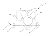
次に、本発明の有機発光素子の他の用途について説明する。図2は、本発明に係る有機発光素子を有する画像形成装置の例を示す模式図である。図2の画像形成装置26は、感光体27と、露光光源28と、現像器30と、帯電部31と、転写器32と、搬送ローラー33と、定着器33と、を有している。
Next, other uses of the organic light emitting device of the present invention will be described. FIG. 2 is a schematic view showing an example of an image forming apparatus having the organic light emitting device according to the present invention. The
図2の画像形成装置26は、露光光源28から感光体27へ向けて光29が照射され、感光体27の表面に静電潜像が形成される。図2の画像形成装置26において、露光光源28は、本発明に係る有機発光素子を複数有している。また図2の画像形成装置26において、現像器30は、トナー等を有している。図2の画像形成装置26において、帯電部31は、感光体27を帯電させるために設けられている。図2の画像形成装置26において、転写器32は、現像された画像を紙等の記録媒体34に転写するために設けられている。尚、記録媒体34は、搬送ローラー33によって転借32へ搬送される。図2の画像形成装置26において、定着器35は、記録媒体34に形成された画像を定着させるために設けられている。
In the
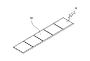
図3(a)及び図3(b)は、図2の画像形成装置26を構成する露光光源の具体例を示す平面概略図であり、図3(c)は、図2の画像形成装置26を構成する感光体の具体例を示す概略図である。尚、図3(a)及び図3(b)は、露光光源28に有機発光素子を含む発光部36が長尺状の基板28aに複数配置されている点で共通している。また符合37の矢印は、発光部36が配列されている列方向を表わす。この列方向は、感光体27が回転する軸の方向と同じである。
3 (a) and 3 (b) are schematic plan views showing a specific example of the exposure light source constituting the
ところで図3(a)では、発光部36は、感光体27の軸方向に沿って配置した形態である。一方、図3(b)では、第一の列αと第二の列βとのそれぞれにおいて発光部36が列方向に交互に配置されている形態である。図3(b)において、第一の列α及び第二の列βは、それぞれ行方向に異なる位置に配置されている。
Incidentally, in FIG. 3A, the
また図3(b)において、第一の列αは、複数の発光部36αが一定の間隔を空けて配置される一方で、第二の列βは、第一の列αに含まれる発光部36α同士の間隔に対応する位置に発光部36βを有する。即ち、図3(b)の露光光源は、行方向にも、複数の発光部が一定の間隔を空けつつ配置されている。 Further, in FIG. 3B, in the first row α, a plurality of light emitting portions 36α are arranged at a constant interval, while the second row β is a light emitting portion included in the first row α. The light emitting unit 36β is provided at a position corresponding to the interval between the 36α. That is, in the exposure light source of FIG. 3B, a plurality of light emitting units are arranged in the row direction with a predetermined interval.
尚、図3(b)の露光光源は、露光光源を構成する発光部(36α、36β)を、例えば、格子状、千鳥格子、あるいは市松模様に配置されている状態と言い換えることもできる。 In addition, the exposure light source of FIG.3 (b) can also be paraphrased in the state which has arrange | positioned the light emission parts (36 (alpha), 36 (beta)) which comprise an exposure light source, for example in a grid | lattice form, a staggered pattern, or a checkered pattern.
図4は、本発明に係る有機発光素子を有する照明装置の例を示す模式図である。図4の照明装置は、基板(不図示)の上に設けられる有機発光素子38と、AC/DCコンバーター回路39と、を有している。また図4の照明装置は、装置内の熱を外部へ放出する放熱部に相当する放熱板(不図示)を、例えば、有機発光素子38が載置されている側とは反対側の基板面に有していてもよい。
FIG. 4 is a schematic view showing an example of a lighting device having an organic light emitting element according to the present invention. The lighting apparatus of FIG. 4 includes an organic
[一般式[1]の有機化合物の他の用途]
ところで、一般式[1]の有機化合物は、化合物が有する電子注入性から有機発光素子以外の有機電界素子の構成材料、具体的には、電子を注入する機能を有する部材の構成材料として利用することができる。ここでいう有機電界素子は、一対の電極と、これら一対の電極間に配置され一般式[1]の有機化合物を有する有機機能層と、を有する電界素子である。一般式[1]が利用可能な有機発光素子以外の有機電界素子として、例えば、有機薄膜トランジスタ(有機TFT)、有機太陽電池等の非発光型の電界素子が挙げられる。
[Other uses of organic compound of general formula [1]]
By the way, the organic compound of the general formula [1] is used as a constituent material of an organic electric field element other than the organic light emitting element from the electron injectability possessed by the compound, specifically, a constituent material of a member having a function of injecting electrons. be able to. An organic electric field element here is an electric field element which has a pair of electrodes and an organic functional layer which has an organic compound of general formula [1] arranged between a pair of these electrodes. Examples of the organic electric field element other than the organic light emitting element that can use the general formula [1] include non-light emitting type electric field elements such as an organic thin film transistor (organic TFT) and an organic solar cell.
以下、実施例により本発明を詳細に説明するが、本発明はこれら実施例に限定されるものではない。 EXAMPLES Hereinafter, although an Example demonstrates this invention in detail, this invention is not limited to these Examples.
[ビアクリジニリデン化合物の合成例]
本発明で用いられる一般式[1]の化合物(ビアクリジニリデン化合物)は、非特許文献3を参考にして合成することができる。具体的には、アセトン等を溶媒として用い、亜鉛を加えた後、濃塩酸を滴下し、原料のアクリドン誘導体b−1及びb−2を加えてから反応溶液を攪拌することで合成できる。しかし、一般式[1]の化合物の合成法は、非特許文献3以外の方法を採用しても構わない。
[Synthesis Example of Biakurijini Li Den Compound]
The compounds of the general formula [1] used in the present invention (Biakurijini Li Den compound), a non-patent document 3 can be synthesized with reference. Specifically, using acetone or the like as a solvent, after the addition of zinc was added dropwise concentrated hydrochloric acid, the reaction solution after adding the acridone derivative b-1及beauty b -2 ingredients can be synthesized by stirring. However, methods other than Non-Patent Document 3 may be employed as the method for synthesizing the compound of the general formula [1].
(合成例1)例示化合物A−1の合成
以下に示すスキームに従って、化合物A−1を合成した。
Synthesis Example 1 Synthesis of Exemplary Compound A-1 Compound A-1 was synthesized according to the scheme shown below.
(1)化合物b−13の合成
まず200mlの三ツ口フラスコを用意し、このフラスコ内に、下記に示される試薬を入れた。
化合物b−11:1.50g(7.68mmol)
化合物b−12:2.41g(15.36mmol)
ナトリウムターシャリブトキシド:1.47g(15.36mmol)
(1) Synthesis of Compound b-13 First, a 200 ml three-necked flask was prepared, and the reagents shown below were put into the flask.
Compound b-11: 1.50 g (7.68 mmol)
Compound b-12: 2.41 g (15.36 mmol)
Sodium tersalibutoxide: 1.47 g (15.36 mmol)
次に、クロロベンゼン100mlを入れた後、窒素雰囲気中、室温下で反応溶液を攪拌しながら、トリターシャリブチルフォスフィン155mgを添加した。次いで酢酸パラジウム86mgを添加した。次に、反応溶液を131℃に昇温した後、この温度(131℃)で5時間攪拌した。反応終了後、水100mlを入れた後、クロロホルムを用いて有機層を抽出した。次に、有機層を無水硫酸ナトリウムで乾燥させた後、減圧濃縮することで粗生成物を得た。次に、この粗生成物を、シリカゲルカラム(トルエン+酢酸エチル混合展開溶媒)で精製することで、化合物b−13を白色固体として1.31g(収率63%)得た。 Next, 100 ml of chlorobenzene was added, and 155 mg of tritertiary butylphosphine was added while stirring the reaction solution at room temperature in a nitrogen atmosphere. Then 86 mg of palladium acetate was added. Next, the reaction solution was heated to 131 ° C., and then stirred at this temperature (131 ° C.) for 5 hours. After completion of the reaction, 100 ml of water was added and the organic layer was extracted with chloroform. Next, the organic layer was dried over anhydrous sodium sulfate and then concentrated under reduced pressure to obtain a crude product. Next, the crude product was purified with a silica gel column (toluene + ethyl acetate mixed developing solvent) to obtain 1.31 g (yield 63%) of a compound b-13 as a white solid.
(2)例示化合物A−1の合成
まず50ml三ツ口フラスコを用意し、このフラスコ内に、アセトン30mlを入れた後、アルゴンで15分、バブリングした。次に、フラスコ内に、以下に示される試薬を入れた。
化合物b−13:271mg(1.0mmol)
亜鉛粉:1.30g(20.0mmol)
(2) Synthesis of Exemplified Compound A-1 First, a 50 ml three-necked flask was prepared, 30 ml of acetone was put into this flask, and then bubbled with argon for 15 minutes. Next, the following reagents were put in the flask.
Compound b-13: 271 mg (1.0 mmol)
Zinc powder: 1.30 g (20.0 mmol)
次に、反応溶液を50℃に加熱し、この温度(50℃)で30分攪拌した。次に、反応溶液を氷冷させながら、濃塩酸12.0mlを30分かけて滴下後、室温で20時間反応溶液を撹拌することで反応を進行させた。反応終了後、水30mlを入れ、析出した黄色固体をろ過し、水とメタノールで固体を洗浄することにより、例示化合物A−1を黄色固体として177mg(収率69%)を得た。 Next, the reaction solution was heated to 50 ° C. and stirred at this temperature (50 ° C.) for 30 minutes. Next, while cooling the reaction solution with ice, 12.0 ml of concentrated hydrochloric acid was added dropwise over 30 minutes, and then the reaction was allowed to proceed by stirring the reaction solution at room temperature for 20 hours. After completion of the reaction, 30 ml of water was added, the precipitated yellow solid was filtered, and the solid was washed with water and methanol to obtain 177 mg (yield 69%) of Exemplary Compound A-1 as a yellow solid.
質量分析法により、この化合物のM+である510を確認した。また、DSC(示差走査熱量分析)法により、ガラス転移温度245℃を確認した。 By mass spectrometry, 510, which is M + of this compound, was confirmed. Further, a glass transition temperature of 245 ° C. was confirmed by a DSC (differential scanning calorimetry) method.
(合成例2)例示化合物C−2の合成
以下に示すスキームに従って、例示化合物C−2を合成した。
(Synthesis Example 2) Synthesis of Exemplified Compound C-2 Exemplified Compound C-2 was synthesized according to the scheme shown below.
(1)化合物b−15の合成
まず500ml三ツ口フラスコを用意し、このフラスコに、以下に示される試薬を入れた。
化合物b−11:1.20g(4.40mmol)
化合物b−14:2.40g(12.4mmol)
ナトリウムターシャリブトキシド:1.20g(12.5mmol)
(1) Synthesis of Compound b-15 First, a 500 ml three-necked flask was prepared, and the reagent shown below was placed in the flask.
Compound b-11: 1.20 g (4.40 mmol)
Compound b-14: 2.40 g (12.4 mmol)
Sodium tersalibutoxide: 1.20 g (12.5 mmol)
次に、オルトキシレン250mlを入れた後、窒素雰囲気中、室温下で反応溶液を攪拌しながら、トリターシャリブチルフォスフィン120mgを添加した。次いで酢酸パラジウム70mgを添加した。次に、反応溶液を144℃に昇温し、この温度(144℃)で5時間攪拌した。反応終了後、水100mlを入れ、有機層をトルエンで抽出した。次に、有機層を無水硫酸ナトリウムで乾燥させた後、減圧濃縮することで粗生成物を得た。次に、シリカゲルカラムクロマトグラフィー(トルエン+酢酸エチル混合展開溶媒)で精製することで、化合物b−15を、白色固体として0.74g(収率55%)得た。 Next, after adding 250 ml of orthoxylene, 120 mg of tritertiary butylphosphine was added while stirring the reaction solution at room temperature in a nitrogen atmosphere. Then 70 mg of palladium acetate was added. Next, the reaction solution was heated to 144 ° C. and stirred at this temperature (144 ° C.) for 5 hours. After completion of the reaction, 100 ml of water was added, and the organic layer was extracted with toluene. Next, the organic layer was dried over anhydrous sodium sulfate and then concentrated under reduced pressure to obtain a crude product. Next, by refine | purifying with silica gel column chromatography (Toluene + ethyl acetate mixed developing solvent), 0.74 g (yield 55%) of compound b-15 was obtained as a white solid.
(2)例示化合物C−2の合成
まず50ml三ツ口フラスコを用意し、このフラスコ内に、アセトン25mlを入れた後、アルゴンで15分、バブリングした。次に、フラスコ内に、以下に示される試薬を入れた。
化合物b−15:276mg(0.90mmol)
亜鉛粉:1.17g(18.0mmol)
(2) Synthesis of Exemplified Compound C-2 First, a 50 ml three-necked flask was prepared, and 25 ml of acetone was placed in the flask, and then bubbled with argon for 15 minutes. Next, the following reagents were put in the flask.
Compound b-15: 276 mg (0.90 mmol)
Zinc powder: 1.17 g (18.0 mmol)
次に、反応溶液を50℃に加熱し、この温度(50℃)で30分攪拌した。次に、反応溶液を氷冷させながら、濃塩酸10.8mlを30分かけて滴下後、室温で20時間反応溶液を撹拌することで反応を進行させた。反応終了後、水25mlを入れ、析出した黄色固体をろ過し、水とメタノールで固体を洗浄することにより、例示化合物A−1を黄色固体として124mg(収率47%)得た。 Next, the reaction solution was heated to 50 ° C. and stirred at this temperature (50 ° C.) for 30 minutes. Next, while cooling the reaction solution with ice, 10.8 ml of concentrated hydrochloric acid was added dropwise over 30 minutes, and then the reaction was allowed to proceed by stirring the reaction solution at room temperature for 20 hours. After completion of the reaction, 25 ml of water was added, the precipitated yellow solid was filtered, and the solid was washed with water and methanol to obtain 124 mg (yield 47%) of Exemplary Compound A-1 as a yellow solid.
質量分析法により、この化合物のM+である582を確認した。 By mass spectrometry, 582 as M + of this compound was confirmed.
(合成例3乃至8)
合成例2(1)において、化合物b−11に代えて下記表1に示されるアクリドン誘導体を使用し、また化合物b−14に代えて下記表1に示されるハロゲン体を使用したことを除いては、合成例2と同様の方法により下記例示化合物を合成した。
に変えることで合成2と同様にして合成した。
(Synthesis Examples 3 to 8)
In Synthesis Example 2 (1), the compound b-11 is replaced with an acridone derivative shown in the following Table 1, and a compound b-14 is replaced with a halogen shown in the following Table 1 except that Prepared the following exemplary compounds by the same method as in Synthesis Example 2.
Was synthesized in the same manner as in
[実施例1]
本実施例では、基板の上に、陽極、正孔輸送層、発光層、電子輸送層、電子注入層及び陰極がこの順に積層されている有機発光素子を作製した。尚、本実施例において、電子注入層は、二つの層からなる積層体である。ここで、本実施例にて使用した材料の一部を以下に列挙する。
Example 1
In this example, an organic light emitting device was fabricated in which an anode, a hole transport layer, a light emitting layer, an electron transport layer, an electron injection layer, and a cathode were laminated in this order on a substrate. In this embodiment, the electron injection layer is a laminated body composed of two layers. Here, some of the materials used in this example are listed below.
スパッタ法により、ガラス基板(基板)の上に、酸化錫インジウム(ITO)を成膜して陽極を形成した。次に、陽極が形成されている基板を、アセトン、イソプロピルアルコール(IPA)で順次超音波洗浄し、次いでIPAで煮沸洗浄後乾燥した。さらに、UV/オゾン洗浄したものを透明導電性支持基板として次に工程で使用した。 An anode was formed by depositing indium tin oxide (ITO) on a glass substrate (substrate) by sputtering. Next, the substrate on which the anode was formed was ultrasonically washed in turn with acetone and isopropyl alcohol (IPA), then washed by boiling in IPA and dried. Furthermore, what was UV / ozone cleaned was used in the next step as a transparent conductive support substrate.
次に、透明導電性支持基板の上に、下記表2に示される有機化合物層及び電極層を、10-5Paの真空チャンバー内における抵抗加熱による真空蒸着を利用して連続成膜をすることで、有機発光素子を作製した。 Next, the organic compound layer and the electrode layer shown in Table 2 below are continuously formed on the transparent conductive support substrate by using vacuum evaporation by resistance heating in a vacuum chamber of 10 −5 Pa. Thus, an organic light emitting device was produced.
本実施例にて得られた有機発光素子に10Vの印加電圧をかけたところ2.9cd/m2のCIE色度(0.64,0.35)の発光ドーパントh−3由来の赤色発光が観測された。 When an applied voltage of 10 V was applied to the organic light-emitting device obtained in this example, red light emission derived from the light-emitting dopant h-3 having a CIE chromaticity (0.64, 0.35) of 2.9 cd / m 2 was obtained. Observed.
[実施例2乃至6]
実施例1において、電子輸送層、第一電子注入層及び第二電子注入層の組み合わせを、下記表3の通りに変更したこと以外は、実施例1と同様の方法により有機発光素子を作製した。
[Examples 2 to 6]
In Example 1, an organic light emitting device was produced by the same method as in Example 1 except that the combination of the electron transport layer, the first electron injection layer, and the second electron injection layer was changed as shown in Table 3 below. .
また、実施例2乃至6にて使用した材料の一部を以下に列挙する。 Also, some of the materials used in Examples 2 to 6 are listed below.
実施例2乃至6にてそれぞれ作製した有機発光素子について、実施例1と同様の方法で評価を行った。素子評価の結果を下記表4に示す。 The organic light emitting devices produced in Examples 2 to 6 were evaluated in the same manner as in Example 1. The results of element evaluation are shown in Table 4 below.
[実施例7]
実施例1において、介在層及び有機機能層を形成する代わりに、以下に説明する電子注入層を形成したことを除いては、実施例1と同様の方法により、有機発光素子を作製した。
[Example 7]
In Example 1, an organic light emitting device was produced in the same manner as in Example 1 except that instead of forming the intervening layer and the organic functional layer, an electron injection layer described below was formed.
(電子注入層の形成)
電子輸送層の上に、例示化合物A−2及びh−5を、層内の重量濃度比が例示化合物A−2:h−5=50:50となるように共蒸着し、膜厚10nmの電子注入層を形成した。
(Formation of electron injection layer)
On the electron transporting layer, Exemplified Compounds A-2 and h-5 are co-deposited so that the weight concentration ratio in the layer is Exemplified Compound A-2: h-5 = 50: 50, and the film thickness is 10 nm. An electron injection layer was formed.
本実施例の有機発光素子に10Vの印加電圧をかけたところ、2.0cd/m2のCIE色度(0.65,0.35)の発光ドーパントh−3由来の赤色発光が観測された。 When an applied voltage of 10 V was applied to the organic light emitting device of this example, red emission derived from the light emitting dopant h-3 of CIE chromaticity (0.65, 0.35) of 2.0 cd / m 2 was observed. .
18:TFT素子、21:陽極、22:有機化合物層、23:陰極 18: TFT element, 21: anode, 22: organic compound layer, 23: cathode
Claims (14)
前記有機化合物層が、有機機能層を有し、
前記有機機能層が、下記一般式[1]に示される有機化合物を有し、
前記有機機能層が、前記陰極と発光層との間に配置される層であることを特徴とする、有機発光素子。
The organic compound layer has an organic functional layer,
The organic functional layer, have a organic compound represented by the following general formula [1],
The organic light emitting element, wherein the organic functional layer is a layer disposed between the cathode and the light emitting layer .
前記第一の有機化合物が、前記一般式[1]に示される有機化合物であり、
前記第二の有機化合物が、前記一般式[1]に示される有機化合物とは別種の有機化合物であることを特徴とする、請求項5に記載の有機発光素子。 The organic functional layer has a first organic compound and a second organic compound,
The first organic compound is an organic compound represented by the general formula [1],
The organic light-emitting device according to claim 5 , wherein the second organic compound is a different organic compound from the organic compound represented by the general formula [1].
前記有機化合物層が、有機機能層を有し、The organic compound layer has an organic functional layer,
前記有機機能層が、下記一般式[1]に示される有機化合物を有することを特徴とする、有機発光素子。The organic light-emitting element, wherein the organic functional layer has an organic compound represented by the following general formula [1].
前記露光部は、請求項1乃至8のいずれか一項に記載の有機発光素子を有することを特徴とする、画像形成装置。 A photoconductor, a charging unit for charging the surface of the photoconductor, an exposure unit for exposing the photoconductor, and a developing unit for developing an electrostatic latent image formed on the surface of the photoconductor. An image forming apparatus having
The image forming apparatus, wherein the exposure unit includes the organic light-emitting element according to claim 1.
請求項1乃至8のいずれか一項に記載の有機発光素子を複数有し、
前記複数の有機発光素子が、列を形成して配置されていることを特徴とする、露光装置。 An exposure apparatus for exposing a photoreceptor,
It has two or more organic light emitting elements as described in any one of Claims 1 thru | or 8,
An exposure apparatus, wherein the plurality of organic light emitting elements are arranged in a row.
前記有機機能層が、下記一般式[1]に示される有機化合物を有し、
前記有機機能層が、前記陰極に接する層であることを特徴とする、有機電界素子。
The organic functional layer, have a organic compound represented by the following general formula [1],
The organic electric field element, wherein the organic functional layer is a layer in contact with the cathode .
Priority Applications (2)
| Application Number | Priority Date | Filing Date | Title |
|---|---|---|---|
| JP2015007532A JP6552201B2 (en) | 2015-01-19 | 2015-01-19 | Organic light emitting device |
| US14/996,349 US9960366B2 (en) | 2015-01-19 | 2016-01-15 | Organic light emitting element |
Applications Claiming Priority (1)
| Application Number | Priority Date | Filing Date | Title |
|---|---|---|---|
| JP2015007532A JP6552201B2 (en) | 2015-01-19 | 2015-01-19 | Organic light emitting device |
Publications (3)
| Publication Number | Publication Date |
|---|---|
| JP2016134470A JP2016134470A (en) | 2016-07-25 |
| JP2016134470A5 JP2016134470A5 (en) | 2018-02-08 |
| JP6552201B2 true JP6552201B2 (en) | 2019-07-31 |
Family
ID=56408478
Family Applications (1)
| Application Number | Title | Priority Date | Filing Date |
|---|---|---|---|
| JP2015007532A Active JP6552201B2 (en) | 2015-01-19 | 2015-01-19 | Organic light emitting device |
Country Status (2)
| Country | Link |
|---|---|
| US (1) | US9960366B2 (en) |
| JP (1) | JP6552201B2 (en) |
Families Citing this family (4)
| Publication number | Priority date | Publication date | Assignee | Title |
|---|---|---|---|---|
| US11342189B2 (en) * | 2015-09-17 | 2022-05-24 | Semiconductor Components Industries, Llc | Semiconductor packages with die including cavities and related methods |
| DE102017101077B4 (en) * | 2017-01-20 | 2025-06-26 | Pictiva Displays International Limited | Organic electronic component |
| CN108516970B (en) * | 2018-04-25 | 2021-01-19 | 华南理工大学 | Heterocyclic bridged phenyl ethylene derivatives, and preparation method and application thereof |
| CN111039924A (en) * | 2019-11-26 | 2020-04-21 | 武汉华星光电半导体显示技术有限公司 | Hole transport material with ethylene bisacridine as core and organic light-emitting diode |
Family Cites Families (20)
| Publication number | Priority date | Publication date | Assignee | Title |
|---|---|---|---|---|
| JP3409356B2 (en) * | 1993-04-09 | 2003-05-26 | 東洋インキ製造株式会社 | Organic electroluminescence device |
| JP3779849B2 (en) * | 1999-10-18 | 2006-05-31 | 大日精化工業株式会社 | Method for producing chemiluminescent reagent |
| US6897036B2 (en) * | 2002-06-06 | 2005-05-24 | Lumigen, Inc. | Fluorescent detection of peroxidase enzymes |
| JP2004051490A (en) * | 2002-07-16 | 2004-02-19 | Nissan Chem Ind Ltd | Chemical luminescent compound and its manufacturing method |
| JP4328801B2 (en) | 2005-12-20 | 2009-09-09 | キヤノン株式会社 | Fluorene compound and organic electroluminescence device |
| JP5376857B2 (en) | 2008-08-04 | 2013-12-25 | キヤノン株式会社 | Fused polycyclic compound and organic light emitting device using the same |
| JP5523060B2 (en) | 2009-03-16 | 2014-06-18 | キヤノン株式会社 | Novel biclicene compound and organic light emitting device having the same |
| JP6016511B2 (en) * | 2012-08-07 | 2016-10-26 | キヤノン株式会社 | Novel condensed polycyclic compound, organic light emitting device having the same, display device, image information processing device, illumination device, and image forming device |
| JP5911418B2 (en) | 2012-12-27 | 2016-04-27 | キヤノン株式会社 | Organic light emitting device |
| JP5911419B2 (en) | 2012-12-27 | 2016-04-27 | キヤノン株式会社 | Organic light emitting device and display device |
| JP5818870B2 (en) | 2012-12-27 | 2015-11-18 | キヤノン株式会社 | Organic light emitting device and display device |
| JP6071569B2 (en) | 2013-01-17 | 2017-02-01 | キヤノン株式会社 | Organic light emitting device |
| JP6222931B2 (en) | 2013-01-21 | 2017-11-01 | キヤノン株式会社 | Organic light emitting device |
| JP5984689B2 (en) | 2013-01-21 | 2016-09-06 | キヤノン株式会社 | Organometallic complex and organic light emitting device using the same |
| JP6095391B2 (en) | 2013-02-06 | 2017-03-15 | キヤノン株式会社 | Organic light emitting device |
| JP6095390B2 (en) | 2013-02-06 | 2017-03-15 | キヤノン株式会社 | Organic light emitting device and display device |
| JP6444046B2 (en) | 2013-04-03 | 2018-12-26 | キヤノン株式会社 | Organic compound and organic light emitting device |
| JP6335530B2 (en) | 2014-01-29 | 2018-05-30 | キヤノン株式会社 | Organic light emitting device |
| JP6448369B2 (en) * | 2014-02-03 | 2019-01-09 | キヤノン株式会社 | Organic light emitting device |
| JP6472246B2 (en) | 2014-03-24 | 2019-02-20 | キヤノン株式会社 | Organic light emitting device |
-
2015
- 2015-01-19 JP JP2015007532A patent/JP6552201B2/en active Active
-
2016
- 2016-01-15 US US14/996,349 patent/US9960366B2/en active Active
Also Published As
| Publication number | Publication date |
|---|---|
| US20160211467A1 (en) | 2016-07-21 |
| JP2016134470A (en) | 2016-07-25 |
| US9960366B2 (en) | 2018-05-01 |
Similar Documents
| Publication | Publication Date | Title |
|---|---|---|
| CN111357128B (en) | Materials for organic devices, organic electroluminescent devices, display devices, and lighting devices | |
| EP2939289B1 (en) | Organic light-emitting element | |
| EP2939287B1 (en) | Organic light-emitting element and display apparatus | |
| JP6270735B2 (en) | Aromatic amine derivative and organic electroluminescence device | |
| CN107210382B (en) | Organic electroluminescent device | |
| JP4659695B2 (en) | Fluorene compound and organic light emitting device | |
| WO2014199637A1 (en) | Material for organic electroluminescent elements, organic electroluminescent element using same, and electronic device | |
| KR101802618B1 (en) | Novel organic compound and organic light-emitting device and display apparatus having the same | |
| US20160141506A1 (en) | NAPHTHO[2,1-b]FLUORANTHENE COMPOUND, ORGANIC LIGHT-EMITTING DEVICE, DISPLAY APPARATUS, LIGHTING APPARATUS, IMAGE FORMING APPARATUS, AND EXPOSING APPARATUS | |
| JP6472246B2 (en) | Organic light emitting device | |
| EP2589596A1 (en) | Aromatic amine derivative, and organic electroluminescent element comprising same | |
| JP6271853B2 (en) | Organic light emitting device, display device, image information processing apparatus, and image forming apparatus | |
| JP6226728B2 (en) | Organic light emitting device and display device | |
| JP6448369B2 (en) | Organic light emitting device | |
| JP6444046B2 (en) | Organic compound and organic light emitting device | |
| JP6552201B2 (en) | Organic light emitting device | |
| JP6226727B2 (en) | Organic light emitting device and display device | |
| WO2011121935A1 (en) | Novel organic compound and organic light-emitting device | |
| WO2011018951A1 (en) | Pyrene derivative and organic light-emitting device using the same | |
| JP7784874B2 (en) | Triazine Compounds | |
| JP2015153993A (en) | organic light-emitting element | |
| KR101584855B1 (en) | Nitrogen-containing heterocyclic compounds and organic electronic device comprising the same | |
| WO2010058855A1 (en) | Novel organic compound, light-emitting device, and image display apparatus | |
| JP5534705B2 (en) | Novel condensed polycyclic compounds and organic light emitting devices | |
| JP2015227299A (en) | Organic compound, organic light emitting device and display device |
Legal Events
| Date | Code | Title | Description |
|---|---|---|---|
| A521 | Request for written amendment filed |
Free format text: JAPANESE INTERMEDIATE CODE: A523 Effective date: 20171220 |
|
| A621 | Written request for application examination |
Free format text: JAPANESE INTERMEDIATE CODE: A621 Effective date: 20171220 |
|
| A131 | Notification of reasons for refusal |
Free format text: JAPANESE INTERMEDIATE CODE: A131 Effective date: 20190108 |
|
| A521 | Request for written amendment filed |
Free format text: JAPANESE INTERMEDIATE CODE: A523 Effective date: 20190307 |
|
| TRDD | Decision of grant or rejection written | ||
| A01 | Written decision to grant a patent or to grant a registration (utility model) |
Free format text: JAPANESE INTERMEDIATE CODE: A01 Effective date: 20190604 |
|
| A61 | First payment of annual fees (during grant procedure) |
Free format text: JAPANESE INTERMEDIATE CODE: A61 Effective date: 20190702 |
|
| R151 | Written notification of patent or utility model registration |
Ref document number: 6552201 Country of ref document: JP Free format text: JAPANESE INTERMEDIATE CODE: R151 |