JP6538007B2 - Elastic wave device - Google Patents
Elastic wave device Download PDFInfo
- Publication number
- JP6538007B2 JP6538007B2 JP2016129230A JP2016129230A JP6538007B2 JP 6538007 B2 JP6538007 B2 JP 6538007B2 JP 2016129230 A JP2016129230 A JP 2016129230A JP 2016129230 A JP2016129230 A JP 2016129230A JP 6538007 B2 JP6538007 B2 JP 6538007B2
- Authority
- JP
- Japan
- Prior art keywords
- film
- region
- divided
- resonance
- resonators
- Prior art date
- Legal status (The legal status is an assumption and is not a legal conclusion. Google has not performed a legal analysis and makes no representation as to the accuracy of the status listed.)
- Active
Links
- 239000010408 film Substances 0.000 claims description 239
- 239000010409 thin film Substances 0.000 claims description 66
- 238000003780 insertion Methods 0.000 claims description 54
- 230000037431 insertion Effects 0.000 claims description 54
- 239000000758 substrate Substances 0.000 claims description 36
- 230000002093 peripheral effect Effects 0.000 claims description 13
- 230000005484 gravity Effects 0.000 claims description 3
- 239000012528 membrane Substances 0.000 claims 1
- 230000004048 modification Effects 0.000 description 61
- 238000012986 modification Methods 0.000 description 61
- 239000010410 layer Substances 0.000 description 39
- 230000005540 biological transmission Effects 0.000 description 15
- 230000000052 comparative effect Effects 0.000 description 12
- 238000010586 diagram Methods 0.000 description 12
- 230000003071 parasitic effect Effects 0.000 description 10
- VYPSYNLAJGMNEJ-UHFFFAOYSA-N Silicium dioxide Chemical compound O=[Si]=O VYPSYNLAJGMNEJ-UHFFFAOYSA-N 0.000 description 8
- 239000011651 chromium Substances 0.000 description 8
- PMHQVHHXPFUNSP-UHFFFAOYSA-M copper(1+);methylsulfanylmethane;bromide Chemical compound Br[Cu].CSC PMHQVHHXPFUNSP-UHFFFAOYSA-M 0.000 description 8
- 229910052814 silicon oxide Inorganic materials 0.000 description 7
- 239000010936 titanium Substances 0.000 description 7
- 230000006378 damage Effects 0.000 description 6
- 239000011800 void material Substances 0.000 description 6
- XLOMVQKBTHCTTD-UHFFFAOYSA-N Zinc monoxide Chemical compound [Zn]=O XLOMVQKBTHCTTD-UHFFFAOYSA-N 0.000 description 5
- 239000010949 copper Substances 0.000 description 4
- 230000006866 deterioration Effects 0.000 description 4
- 229910052802 copper Inorganic materials 0.000 description 3
- 230000005684 electric field Effects 0.000 description 3
- 229910052751 metal Inorganic materials 0.000 description 3
- 239000002184 metal Substances 0.000 description 3
- 229910052750 molybdenum Inorganic materials 0.000 description 3
- BASFCYQUMIYNBI-UHFFFAOYSA-N platinum Substances [Pt] BASFCYQUMIYNBI-UHFFFAOYSA-N 0.000 description 3
- 229910052703 rhodium Inorganic materials 0.000 description 3
- 239000010948 rhodium Substances 0.000 description 3
- 229910052719 titanium Inorganic materials 0.000 description 3
- PIGFYZPCRLYGLF-UHFFFAOYSA-N Aluminum nitride Chemical compound [Al]#N PIGFYZPCRLYGLF-UHFFFAOYSA-N 0.000 description 2
- 229910052581 Si3N4 Inorganic materials 0.000 description 2
- ATJFFYVFTNAWJD-UHFFFAOYSA-N Tin Chemical group [Sn] ATJFFYVFTNAWJD-UHFFFAOYSA-N 0.000 description 2
- 229910052782 aluminium Inorganic materials 0.000 description 2
- 239000011575 calcium Substances 0.000 description 2
- 229910052804 chromium Inorganic materials 0.000 description 2
- 230000008878 coupling Effects 0.000 description 2
- 238000010168 coupling process Methods 0.000 description 2
- 238000005859 coupling reaction Methods 0.000 description 2
- 230000000694 effects Effects 0.000 description 2
- 239000010931 gold Substances 0.000 description 2
- 229910021480 group 4 element Inorganic materials 0.000 description 2
- 229910021478 group 5 element Inorganic materials 0.000 description 2
- 229910052741 iridium Inorganic materials 0.000 description 2
- HFGPZNIAWCZYJU-UHFFFAOYSA-N lead zirconate titanate Chemical compound [O-2].[O-2].[O-2].[O-2].[O-2].[Ti+4].[Zr+4].[Pb+2] HFGPZNIAWCZYJU-UHFFFAOYSA-N 0.000 description 2
- 229910052451 lead zirconate titanate Inorganic materials 0.000 description 2
- 239000011777 magnesium Substances 0.000 description 2
- 229910052758 niobium Inorganic materials 0.000 description 2
- 239000010955 niobium Substances 0.000 description 2
- 230000010287 polarization Effects 0.000 description 2
- 229910052707 ruthenium Inorganic materials 0.000 description 2
- HQVNEWCFYHHQES-UHFFFAOYSA-N silicon nitride Chemical compound N12[Si]34N5[Si]62N3[Si]51N64 HQVNEWCFYHHQES-UHFFFAOYSA-N 0.000 description 2
- 239000002356 single layer Substances 0.000 description 2
- 229910052715 tantalum Inorganic materials 0.000 description 2
- 229910052721 tungsten Inorganic materials 0.000 description 2
- 239000011701 zinc Substances 0.000 description 2
- 239000011787 zinc oxide Substances 0.000 description 2
- 229910052726 zirconium Inorganic materials 0.000 description 2
- ZOXJGFHDIHLPTG-UHFFFAOYSA-N Boron Chemical compound [B] ZOXJGFHDIHLPTG-UHFFFAOYSA-N 0.000 description 1
- OYPRJOBELJOOCE-UHFFFAOYSA-N Calcium Chemical compound [Ca] OYPRJOBELJOOCE-UHFFFAOYSA-N 0.000 description 1
- VYZAMTAEIAYCRO-UHFFFAOYSA-N Chromium Chemical compound [Cr] VYZAMTAEIAYCRO-UHFFFAOYSA-N 0.000 description 1
- RYGMFSIKBFXOCR-UHFFFAOYSA-N Copper Chemical compound [Cu] RYGMFSIKBFXOCR-UHFFFAOYSA-N 0.000 description 1
- 229910001218 Gallium arsenide Inorganic materials 0.000 description 1
- FYYHWMGAXLPEAU-UHFFFAOYSA-N Magnesium Chemical compound [Mg] FYYHWMGAXLPEAU-UHFFFAOYSA-N 0.000 description 1
- ZOKXTWBITQBERF-UHFFFAOYSA-N Molybdenum Chemical compound [Mo] ZOKXTWBITQBERF-UHFFFAOYSA-N 0.000 description 1
- KJTLSVCANCCWHF-UHFFFAOYSA-N Ruthenium Chemical compound [Ru] KJTLSVCANCCWHF-UHFFFAOYSA-N 0.000 description 1
- 229910004298 SiO 2 Inorganic materials 0.000 description 1
- XUIMIQQOPSSXEZ-UHFFFAOYSA-N Silicon Chemical compound [Si] XUIMIQQOPSSXEZ-UHFFFAOYSA-N 0.000 description 1
- RTAQQCXQSZGOHL-UHFFFAOYSA-N Titanium Chemical compound [Ti] RTAQQCXQSZGOHL-UHFFFAOYSA-N 0.000 description 1
- HCHKCACWOHOZIP-UHFFFAOYSA-N Zinc Chemical compound [Zn] HCHKCACWOHOZIP-UHFFFAOYSA-N 0.000 description 1
- QCWXUUIWCKQGHC-UHFFFAOYSA-N Zirconium Chemical compound [Zr] QCWXUUIWCKQGHC-UHFFFAOYSA-N 0.000 description 1
- 239000000654 additive Substances 0.000 description 1
- 230000000996 additive effect Effects 0.000 description 1
- PNEYBMLMFCGWSK-UHFFFAOYSA-N aluminium oxide Inorganic materials [O-2].[O-2].[O-2].[Al+3].[Al+3] PNEYBMLMFCGWSK-UHFFFAOYSA-N 0.000 description 1
- 229910052796 boron Inorganic materials 0.000 description 1
- 229910052791 calcium Inorganic materials 0.000 description 1
- 239000000919 ceramic Substances 0.000 description 1
- NKZSPGSOXYXWQA-UHFFFAOYSA-N dioxido(oxo)titanium;lead(2+) Chemical compound [Pb+2].[O-][Ti]([O-])=O NKZSPGSOXYXWQA-UHFFFAOYSA-N 0.000 description 1
- 238000006073 displacement reaction Methods 0.000 description 1
- 239000011521 glass Substances 0.000 description 1
- PCHJSUWPFVWCPO-UHFFFAOYSA-N gold Chemical compound [Au] PCHJSUWPFVWCPO-UHFFFAOYSA-N 0.000 description 1
- 229910052737 gold Inorganic materials 0.000 description 1
- 229910052735 hafnium Inorganic materials 0.000 description 1
- VBJZVLUMGGDVMO-UHFFFAOYSA-N hafnium atom Chemical compound [Hf] VBJZVLUMGGDVMO-UHFFFAOYSA-N 0.000 description 1
- GKOZUEZYRPOHIO-UHFFFAOYSA-N iridium atom Chemical compound [Ir] GKOZUEZYRPOHIO-UHFFFAOYSA-N 0.000 description 1
- 229910052749 magnesium Inorganic materials 0.000 description 1
- 238000004519 manufacturing process Methods 0.000 description 1
- 229910044991 metal oxide Inorganic materials 0.000 description 1
- 150000004706 metal oxides Chemical class 0.000 description 1
- 239000011733 molybdenum Substances 0.000 description 1
- GUCVJGMIXFAOAE-UHFFFAOYSA-N niobium atom Chemical compound [Nb] GUCVJGMIXFAOAE-UHFFFAOYSA-N 0.000 description 1
- 150000004767 nitrides Chemical class 0.000 description 1
- 238000002161 passivation Methods 0.000 description 1
- 229910052697 platinum Inorganic materials 0.000 description 1
- 230000001902 propagating effect Effects 0.000 description 1
- 239000010453 quartz Substances 0.000 description 1
- MHOVAHRLVXNVSD-UHFFFAOYSA-N rhodium atom Chemical compound [Rh] MHOVAHRLVXNVSD-UHFFFAOYSA-N 0.000 description 1
- 229910052594 sapphire Inorganic materials 0.000 description 1
- 239000010980 sapphire Substances 0.000 description 1
- 229910052706 scandium Inorganic materials 0.000 description 1
- SIXSYDAISGFNSX-UHFFFAOYSA-N scandium atom Chemical compound [Sc] SIXSYDAISGFNSX-UHFFFAOYSA-N 0.000 description 1
- 230000011218 segmentation Effects 0.000 description 1
- 238000000926 separation method Methods 0.000 description 1
- 229910052710 silicon Inorganic materials 0.000 description 1
- 239000010703 silicon Substances 0.000 description 1
- 229910000679 solder Inorganic materials 0.000 description 1
- 239000011029 spinel Substances 0.000 description 1
- 229910052596 spinel Inorganic materials 0.000 description 1
- 229910052712 strontium Inorganic materials 0.000 description 1
- CIOAGBVUUVVLOB-UHFFFAOYSA-N strontium atom Chemical compound [Sr] CIOAGBVUUVVLOB-UHFFFAOYSA-N 0.000 description 1
- GUVRBAGPIYLISA-UHFFFAOYSA-N tantalum atom Chemical compound [Ta] GUVRBAGPIYLISA-UHFFFAOYSA-N 0.000 description 1
- WFKWXMTUELFFGS-UHFFFAOYSA-N tungsten Chemical compound [W] WFKWXMTUELFFGS-UHFFFAOYSA-N 0.000 description 1
- 239000010937 tungsten Substances 0.000 description 1
- 229910052720 vanadium Inorganic materials 0.000 description 1
- LEONUFNNVUYDNQ-UHFFFAOYSA-N vanadium atom Chemical compound [V] LEONUFNNVUYDNQ-UHFFFAOYSA-N 0.000 description 1
- 229910052725 zinc Inorganic materials 0.000 description 1
Images


Classifications
-
- H—ELECTRICITY
- H03—ELECTRONIC CIRCUITRY
- H03H—IMPEDANCE NETWORKS, e.g. RESONANT CIRCUITS; RESONATORS
- H03H9/00—Networks comprising electromechanical or electro-acoustic devices; Electromechanical resonators
- H03H9/02—Details
- H03H9/02007—Details of bulk acoustic wave devices
- H03H9/02086—Means for compensation or elimination of undesirable effects
- H03H9/02133—Means for compensation or elimination of undesirable effects of stress
-
- H—ELECTRICITY
- H03—ELECTRONIC CIRCUITRY
- H03H—IMPEDANCE NETWORKS, e.g. RESONANT CIRCUITS; RESONATORS
- H03H9/00—Networks comprising electromechanical or electro-acoustic devices; Electromechanical resonators
- H03H9/15—Constructional features of resonators consisting of piezoelectric or electrostrictive material
- H03H9/17—Constructional features of resonators consisting of piezoelectric or electrostrictive material having a single resonator
- H03H9/171—Constructional features of resonators consisting of piezoelectric or electrostrictive material having a single resonator implemented with thin-film techniques, i.e. of the film bulk acoustic resonator [FBAR] type
- H03H9/172—Means for mounting on a substrate, i.e. means constituting the material interface confining the waves to a volume
- H03H9/173—Air-gaps
-
- H—ELECTRICITY
- H03—ELECTRONIC CIRCUITRY
- H03H—IMPEDANCE NETWORKS, e.g. RESONANT CIRCUITS; RESONATORS
- H03H9/00—Networks comprising electromechanical or electro-acoustic devices; Electromechanical resonators
- H03H9/15—Constructional features of resonators consisting of piezoelectric or electrostrictive material
- H03H9/205—Constructional features of resonators consisting of piezoelectric or electrostrictive material having multiple resonators
-
- H—ELECTRICITY
- H03—ELECTRONIC CIRCUITRY
- H03H—IMPEDANCE NETWORKS, e.g. RESONANT CIRCUITS; RESONATORS
- H03H9/00—Networks comprising electromechanical or electro-acoustic devices; Electromechanical resonators
- H03H9/46—Filters
- H03H9/54—Filters comprising resonators of piezo-electric or electrostrictive material
- H03H9/56—Monolithic crystal filters
- H03H9/566—Electric coupling means therefor
- H03H9/568—Electric coupling means therefor consisting of a ladder configuration
Landscapes
- Physics & Mathematics (AREA)
- Acoustics & Sound (AREA)
- Chemical & Material Sciences (AREA)
- Crystallography & Structural Chemistry (AREA)
- Piezo-Electric Or Mechanical Vibrators, Or Delay Or Filter Circuits (AREA)
Description
本発明は、弾性波デバイスに関し、例えば圧電薄膜共振器を有する弾性波デバイス関する。 The present invention relates to an elastic wave device, for example, an elastic wave device having a piezoelectric thin film resonator.
圧電薄膜共振器を用いた弾性波デバイスは、例えば携帯電話等の無線機器のフィルタおよびマルチプレクサとして用いられている。圧電薄膜共振器は、圧電膜を挟み下部電極と上部電極が対向する構造を有している(特許文献1)。圧電膜を挟み下部電極と上部電極が対向する領域が共振領域である。共振領域の下には振動を制限しないように空隙または音響反射膜が設けられる。空隙または音響反射膜は平面視において共振領域を含むように設けられる。 Elastic wave devices using piezoelectric thin film resonators are used, for example, as filters and multiplexers for wireless devices such as mobile phones. The piezoelectric thin film resonator has a structure in which a lower electrode and an upper electrode face each other with the piezoelectric film interposed therebetween (Patent Document 1). A region in which the lower electrode and the upper electrode face each other with the piezoelectric film interposed therebetween is a resonant region. An air gap or an acoustic reflection film is provided under the resonance region so as not to limit the vibration. The air gap or the acoustic reflection film is provided so as to include the resonance region in plan view.
平面視において、単一の空隙に複数の圧電薄膜共振器が含まれるように配置することが知られている(例えば特許文献1)。空隙を共有しない隣接する圧電薄膜共振器同士で下部電極を共有することが知られている(例えば特許文献2)。圧電膜内の外周領域に挿入膜を設けることが知られている(例えば特許文献3)圧電膜の分極方向が2次歪を抑制するように共振器を分割することが知られている(例えば特許文献4、5)。
It is known that, in a plan view, a plurality of piezoelectric thin film resonators are arranged so as to be included in a single air gap (for example, Patent Document 1). It is known that lower electrodes are shared between adjacent piezoelectric thin film resonators that do not share a gap (for example, Patent Document 2). It is known to provide an insertion film in the outer peripheral region in the piezoelectric film (for example, Patent Document 3). It is known to divide the resonator so that the polarization direction of the piezoelectric film suppresses second-order distortion (for example,
例えば特許文献4、5のように2次歪を抑制するように共振器を分割する場合、特許文献2のように隣接する圧電薄膜共振器の下部電極を共有することが考えられる。しかし、隣接する圧電薄膜共振器を接続する下部電極等が長くなると分割した共振器間で2次歪みが完全にキャンセルされない。特許文献1のように、単一の空隙に複数の圧電薄膜共振器を設けると圧電薄膜共振器間を短くできる。しかし、単一の空隙に複雑な構造を設けるため、積層膜等にクラック等の破壊が生じることがある。
For example, when dividing a resonator so as to suppress second-order distortion as in
本発明は上記課題に鑑みなされたものであり、積層膜等の破壊等を抑制することを目的とする。 The present invention has been made in view of the above problems, and an object thereof is to suppress destruction or the like of a laminated film or the like.
本発明は、基板と、前記基板内または上に設けられた空隙である音響反射層と、前記基板および前記音響反射層上に設けられた圧電膜と、複数の共振領域が平面視において前記音響反射層内に共通に設けられるように、下部電極および上部電極のいずれか一方が分断され前記下部電極および前記上部電極の他方は分断されず、前記基板および前記音響反射層上に前記圧電膜を挟むように設けられた下部電極および上部電極と、前記下部電極と前記上部電極との間に設けられ、平面視において前記複数の共振領域の各々の外周領域において少なくとも一部に設けられ、前記複数の共振領域の各々の中央領域には設けられていない挿入膜と、を具備し、前記複数の共振領域は各々前記圧電膜の少なくとも一部を挟み前記下部電極と前記上部電極とが対向する領域であり、前記挿入膜は平面視において前記下部電極および前記上部電極のいずれか一方が分断された分断領域に重なり、前記分断領域は平面視において前記音響反射層と重なる弾性波デバイスである。 In the present invention, a substrate , an acoustic reflection layer which is an air gap provided in or on the substrate, a piezoelectric film provided on the substrate and the acoustic reflection layer, and the plurality of resonance regions have the acoustic in plan view One of the lower electrode and the upper electrode is divided so that the other of the lower electrode and the upper electrode is not divided so as to be commonly provided in the reflective layer, and the piezoelectric film is formed on the substrate and the acoustic reflection layer. A plurality of lower electrodes and upper electrodes interposed between the lower electrode and the upper electrode, and at least a portion of each of the outer peripheral regions of the plurality of resonant regions in plan view, anda insertion film not provided in the central region of each of the resonance region, the plurality of the resonance region and the lower electrode sandwiching at least a portion of each said piezoelectric film and said upper electrode A facing area, the intervening layer overlaps the dividing region either one was separated of the lower electrode and the upper electrode in a plan view, the dividing region in the acoustic wave device overlapping with the acoustic reflective layer in a plan view is there.
上記構成において、前記挿入膜は、前記複数の共振領域の各々の中央領域を囲む閉ループ状に設けられている構成とすることができる。 In the above configuration, the insertion film may be provided in a closed loop shape surrounding a central region of each of the plurality of resonant regions.
上記構成において、前記複数の共振領域の各々に設けられた挿入膜は一体として設けられた単一の挿入膜である構成とすることができる。 In the above configuration, the insertion film provided in each of the plurality of resonance regions can be a single insertion film provided integrally.
上記構成において、前記挿入膜は、前記分断領域の全てに重なり、前記分断領域に接する前記外周領域に設けられている構成とすることができる。 In the above configuration, the intervening layer is an overlapping all of the divided regions may be configured provided in the outer peripheral region in contact with the dividing region.
上記構成において、前記挿入膜は、平面視において前記空隙の平面形状の重心と重なる構成とすることができる。 In the above configuration, the intervening layer may be configured to overlap with the center of gravity of the plane shape of the gap in a plan view.
上記構成において、前記分断領域において、前記下部電極が分断されている構成とすることができる。 In the above configuration, in the dividing region, can be configured to the lower electrode is divided.
上記構成において、前記分断領域において、前記上部電極が分断されている構成とすることができる。 In the above configuration, in the dividing region, can be configured to the upper electrode is divided.
上記構成において、前記圧電膜は、下部圧電膜と前記下部圧電膜上に設けられた上部圧電膜とを備え、前記挿入膜は前記下部圧電膜と前記上部圧電膜との間に設けられ、前記分断領域において、前記上部電極および前記上部圧電膜が分断されている構成とすることができる。 In the above configuration, the piezoelectric film includes a lower piezoelectric film and an upper piezoelectric film provided on the lower piezoelectric film, and the insertion film is provided between the lower piezoelectric film and the upper piezoelectric film. The upper electrode and the upper piezoelectric film may be divided in the divided region.
上記構成において、前記複数の共振領域の各々において平面視において共振領域に重なる前記挿入膜の幅は略等しい構成とすることができる。 In the above configuration, the width of the insertion film overlapping the resonance region in plan view in each of the plurality of resonance regions may be substantially equal.
上記構成において、前記複数の共振領域にそれぞれ対応する複数の圧電薄膜共振器を含むフィルタを具備する構成とすることができる。 In the above configuration, a filter including a plurality of piezoelectric thin film resonators respectively corresponding to the plurality of resonance regions can be provided.
上記構成において、入力端子と出力端子との間に直列に接続された1または複数の直列共振器と、前記入力端子と前記出力端子との間に並列に接続された1または複数の並列共振器と、を具備し、前記1または複数の直列共振器および前記1または複数の並列共振器の少なくとも1つは複数の分割共振器に分割されており、前記複数の共振領域はそれぞれ前記複数の分割共振器に対応する構成とすることができる。 In the above configuration, one or more series resonators connected in series between the input terminal and the output terminal, and one or more parallel resonators connected in parallel between the input terminal and the output terminal And at least one of the one or more series resonators and the one or more parallel resonators is divided into a plurality of divided resonators, and the plurality of resonance regions are respectively divided into the plurality of divided resonators. A configuration corresponding to a resonator can be made.
上記構成において、入力端子と出力端子との間に直列に接続された1または複数の直列共振器と、前記入力端子と前記出力端子との間に並列に接続された1または複数の並列共振器と、を具備し、前記複数の共振領域は、前記1または複数の直列共振器の少なくとも1つと前記1または複数の並列共振器の少なくとも1つを含む構成とすることができる。 In the above configuration, one or more series resonators connected in series between the input terminal and the output terminal, and one or more parallel resonators connected in parallel between the input terminal and the output terminal And the plurality of resonant regions may be configured to include at least one of the one or more series resonators and at least one of the one or more parallel resonators.
本発明によれば、積層膜等の破壊等を抑制することができる。 According to the present invention, destruction or the like of a laminated film or the like can be suppressed.
まず、圧電薄膜共振器の2次歪みを抑制する例について説明する。図1(a)および図1(b)は、圧電薄膜共振器の断面図を示す図である。図1(a)に示すように、圧電膜14は下部電極12と上部電極16との間に挟まれている。圧電薄膜共振器80では、共振周波数の波長λの1/2がほぼ圧電膜14の厚さに相当する。つまり、圧電薄膜共振器80は、1/2λ厚み共振を用いている。このため、例えば下部電極12が−のとき、上部電極16は+となる。圧電膜14内の上下の面はそれぞれ+および−のいずれかとなる。
First, an example in which the secondary distortion of the piezoelectric thin film resonator is suppressed will be described. FIG. 1A and FIG. 1B are cross-sectional views of the piezoelectric thin film resonator. As shown in FIG. 1A, the
図1(b)に示すように、2次歪の周波数の波長はほぼ圧電膜14の厚さに相当する。このため、圧電膜14の上下の面が+または−となり、圧電膜14の中心が−または+となるように弾性波が励振する。圧電膜14が上下に対称であれば、2次歪は上部電極16と下部電極12とで同電位となる。このため、2次歪成分は生じない。しかしながら、圧電膜14として例えば窒化アルミニウム(AlN)または酸化亜鉛(ZnO)等を用いる場合、良好な特性を得るために、c軸に配向させる。矢印はc軸配向方向34を示している。このとき、圧電膜14内でc軸方向の対称性が崩れ、電界の分布に偏りが生じる。このため、上部電極16と下部電極12とに電位差が生じる。このように2次歪により発生する電圧を2次歪電圧という。下部電極12から上部電極16の方向がc軸配向方向34のとき、c軸配向方向34の同じ方向に2次歪電圧36が発生する。
As shown in FIG. 1B, the wavelength of the second-order distortion frequency substantially corresponds to the thickness of the
図2(a)および図2(b)は、圧電薄膜共振器を並列に分割した図、図2(c)は直列分割した図である。図2(a)および図2(b)では、圧電薄膜共振器80は端子T1とT2との間で並列に圧電薄膜共振器80aおよび80bに分割されている。圧電薄膜共振器80aおよび80bは同じ静電容量を有するように分割されている。
FIGS. 2A and 2B are diagrams in which the piezoelectric thin film resonators are divided in parallel, and FIG. 2C is a diagram in which the piezoelectric thin film resonators are divided in series. In FIGS. 2A and 2B, the piezoelectric
図2(a)では、圧電薄膜共振器80aと80bとで上部電極16が端子T1に接続され、下部電極12が端子T2に接続されている。これにより、端子T1およびT2に加わる2次歪電圧36の方向が同じとなる。このため、端子T1とT2の間には、圧電薄膜共振器80aと80bとの2次歪電圧36の和の2次歪電圧が加わる。図2(b)では、圧電薄膜共振器80aの上部電極16と圧電薄膜共振器80bの下部電極12とが端子T1に接続され、圧電薄膜共振器80aの下部電極12と圧電薄膜共振器80bの上部電極16が端子T2に接続されている。つまり、c軸配向方向34の逆方向の電極同士が接続されている。これにより、圧電薄膜共振器80aと80bとで2次歪電圧36の方向が逆方向で端子T1およびT2に接続さる。このため、圧電薄膜共振器80aと80bとの2次歪電圧36が相殺される。よって、端子T1およびT2に加わる2次歪電圧を抑制できる。
In FIG. 2A, the
図2(c)に示すように、圧電薄膜共振器80は端子T1とT2との間で直列に圧電薄膜共振器80aおよび80bに分割されている。圧電薄膜共振器80aおよび80bの上部電極16がそれぞれ端子T1およびT2に接続され、圧電薄膜共振器80aおよび80bの下部電極12が接続されている。つまり、c軸配向方向34の同じ方向の電極が接続されている。このため、圧電薄膜共振器80aと80bとの2次歪電圧36が相殺される。よって、端子T1およびT2に加わる2次歪電圧を抑制できる。なお、圧電膜14のc軸配向方向34は圧電膜14の分極方向でもよい。
As shown in FIG. 2C, the piezoelectric
図2(b)および図2(c)のように、2次歪電圧36を相殺する比較例1を説明する。
A comparative example 1 in which the second-
(比較例1)
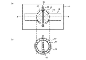
図3(a)は、比較例1に係る弾性波デバイスの平面図、図3(b)および図3(c)は、図3(a)のA−A断面図である。図3(b)は、例えばラダー型フィルタの直列共振器を、図3(c)は例えばラダー型フィルタの並列共振器を示している。
(Comparative example 1)
Fig.3 (a) is a top view of the elastic wave device which concerns on the comparative example 1, FIG.3 (b) and FIG.3 (c) are AA sectional drawings of FIG. 3 (a). FIG. 3 (b) shows, for example, a series resonator of a ladder type filter, and FIG. 3 (c) shows, for example, a parallel resonator of a ladder type filter.
図3(a)から図3(c)に示すように、基板10上に下部電極12、圧電膜14、上部電極16および周波数調整膜24が積層されている。下部電極12は下層12aおよび上層12bを含む。上部電極16は下層16aおよび上層16bを含む。圧電膜14は下部圧電膜14aおよび上部圧電膜14bを含む。下部圧電膜14aと上部圧電膜14bとの間に挿入膜28が設けられている。挿入膜28は、共振領域50の外周領域に設けられている。基板10と下部電極との間には空隙30が形成されている。図3(c)の並列共振器では、上部電極16の下層16aと上層16bとの間に質量負荷膜20が設けられている。直列共振器Sでは、積層膜18は、主に下部電極12、圧電膜14、上部電極16および周波数調整膜24から形成される。並列共振器Pの積層膜18は直列共振器Sの積層膜18に加え、質量負荷膜20を有する。
As shown in FIGS. 3A to 3C, the
2つの圧電薄膜共振器80aおよび80bが下部電極12を介し接続されている。2つの圧電薄膜共振器80aおよび80bは各々空隙30を有している。1つの空隙30内に1つの共振領域50が設けられている、共振領域50間の上部電極16、圧電膜14および挿入膜28は分断され、分断領域62が形成されている。
Two piezoelectric
比較例1では、圧電薄膜共振器80aの共振領域50と圧電薄膜共振器80bの共振領域50との間の下部電極12が空隙30を介さずに基板10上に設けられている。このため、下部電極12とグランドパターン(例えば、圧電薄膜共振器80aおよび80bが形成されたチップに形成されているグランド端子およびグランド配線等のグランドパターン、チップの側面または裏面に形成された半田等の金属層、並びにチップが実装されたパッケージのグランドパターン)との間に寄生容量C0が生じる。
In Comparative Example 1, the
図2(c)のように、圧電薄膜共振器を直列に分割した場合の2次歪電圧をシミュレーションした。2次歪電圧は、圧電薄膜共振器80aおよび80bの圧電膜14に加わる「電界強度の2乗」、「電界強度と歪みの積」および「歪みの2乗」に比例した非線形電流を元に算出した。圧電膜14をc軸に配向した窒化アルミニウム膜とし、圧電薄膜共振器80aおよび80bの同じ静電容量および同じ積層膜18の構造を有するとした。端子T1およびT2のうち一端に28dBmの高周波信号を入力し、他端から出力される2次歪の大きさを算出した。
As shown in FIG. 2C, the second-order distortion voltage was simulated when the piezoelectric thin film resonators were divided in series. The second-order distortion voltage is based on the "square of electric field strength", the "product of electric field strength and distortion" and the "square of distortion" applied to the
図4は、周波数に対する2次歪電圧を示す図である。図4において「分割なし」は分割していない圧電薄膜共振器の2次歪を示している。「分割」は圧電薄膜共振器80aおよび80bに分割した圧電薄膜共振器の2次歪みを示している。「分割」では、圧電薄膜共振器80aおよび80bの間の下部電極12とグランドとの寄生容量C0を0pFから0.01pFまで変化させた。
FIG. 4 is a diagram showing a second-order distortion voltage with respect to frequency. In FIG. 4, “no division” indicates the second-order distortion of the undivided piezoelectric thin film resonator. "Division" indicates the second-order distortion of the piezoelectric thin film resonator divided into the piezoelectric
図4に示すように、分割していない圧電薄膜共振器では、共振周波数frである1895MHzにおける2次歪みは−21.45dBm、反共振周波数faである1953MHzにおける2次歪は−27.83dBm、1913MHzのとき、2次歪は−18.29dBmと最も大きい。分割した圧電薄膜共振器では、寄生容量C0が0pFのとき、2次歪は−65.37dBと非常に小さい。寄生容量C0を0.001pF、0.005pFおよび0.01pFとすると、2次歪は反共振周波数付近で最大となり、それぞれ−54.52dB、−41.4dBおよび−35.4dBとなる。このように、寄生容量C0が大きくなると、反共振周波数付近に発生する2次歪電圧のピークが大きくなる。 As shown in FIG. 4, in the undivided piezoelectric thin film resonator, the secondary distortion at 1895 MHz which is the resonance frequency fr is -21.45 dBm, and the secondary distortion at 1953 MHz which is the antiresonance frequency fa is -27.83 dBm, At 1913 MHz, second-order distortion is the largest at -18.29 dBm. In the divided piezoelectric thin film resonator, when the parasitic capacitance C0 is 0 pF, the second-order distortion is very small at -65.37 dB. Assuming that the parasitic capacitance C0 is 0.001 pF, 0.005 pF and 0.01 pF, the second-order distortion becomes maximum around the antiresonance frequency, and becomes -54.52 dB, -41.4 dB and -35.4 dB, respectively. Thus, as the parasitic capacitance C0 increases, the peak of the secondary distortion voltage generated near the antiresonance frequency increases.
比較例1では、共振領域50の間の下部電極12が基板10上に接している。このため、下部電極12とグランドとの間の寄生容量C0が大きくなる。寄生容量C0が大きくなると、圧電薄膜共振器80aと80bとで反共振周波数が異なってしまう。このように、圧電薄膜共振器80aと80bとで反共振周波数faが異なると、2次歪は完全にはキャンセルされず、反共振周波数fa付近に2次歪のピークが生じる。よって、2次歪を抑制することが難しい。
In Comparative Example 1, the
さらに、2次歪を抑制するためには、圧電薄膜共振器80aと80bの特性は同じであることが好ましい。しかし、比較例1では、圧電薄膜共振器80aと80bとの間の距離が長くなる。このため、圧電薄膜共振器80aと80bとで積層膜18内の各層の膜厚が異なることが生じる。これにより、2次歪が劣化する。
Furthermore, in order to suppress the second-order distortion, it is preferable that the characteristics of the piezoelectric
以下、実施例1について説明する。 Example 1 will be described below.
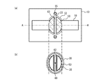
図5(a)は、実施例1に係る弾性波デバイスの平面図、図5(b)は、共振領域付近の平面図、図5(c)および図5(d)は、図5(a)のA−A断面図である。図5(c)は、例えばラダー型フィルタの直列共振器を、図5(d)は例えばラダー型フィルタの並列共振器を示している。 5 (a) is a plan view of the acoustic wave device according to the first embodiment, FIG. 5 (b) is a plan view near the resonance region, and FIGS. 5 (c) and 5 (d) are FIGS. ) Of FIG. 5C shows, for example, a series resonator of a ladder type filter, and FIG. 5D shows, for example, a parallel resonator of a ladder type filter.
図5(a)、図5(b)および図5(d)に示すように、直列共振器Sの構造について説明する。シリコン(Si)基板である基板10および空隙30上に、下部電極12が設けられている。下部電極12はCr(クロム)膜である下層12aおよびRu(ルテニウム)膜である上層12bを含む。基板10の平坦主面と下部電極12との間にドーム状の膨らみを有する空隙30(空気層)が形成されている。ドーム状の膨らみとは、例えば空隙30の周辺では空隙30の高さが小さく、空隙30の内部ほど空隙30の高さが大きくなるような形状の膨らみである。
As shown in FIGS. 5 (a), 5 (b) and 5 (d), the structure of the series resonator S will be described. The
下部電極12上に、(002)方向を主軸とする窒化アルミニウム(AlN)を主成分とする圧電膜14が設けられている。圧電膜14は下部圧電膜14aおよび上部圧電膜14bを含む。下部圧電膜14aと上部圧電膜14bとの間に挿入膜28が設けられている。圧電膜14上に上部電極16が設けられている。上部電極16が分断された分断領域62が設けられている。上部電極16はRu膜である下層12aとCr膜である上層16bとを含む。
A
圧電膜14の少なくとも一部を挟み下部電極12と上部電極16が対向する領域が共振領域50である。上部電極16が分断されている領域が分断領域62である。分断領域62のため、単一の空隙30内に2つの共振領域50が形成されている。共振領域50は、半楕円形状を有し、厚み縦振動モードの弾性波が共振する領域である。共振領域50は、平面視において空隙30と同じまたは空隙30より小さくかつ空隙30と重なるように設けられている。
A region in which the
上部電極16上には周波数調整膜24として酸化シリコン膜が形成されている。共振領域50内の積層膜18は、下部電極12、圧電膜14、上部電極16および周波数調整膜24を含む。周波数調整膜24はパッシベーション膜として機能してもよい。
A silicon oxide film is formed on the
図5(a)のように、圧電膜14および下部電極12には孔部35が設けられている。孔部35は、下部電極12下の導入路33を介し空隙30に通じている。孔部35および導入路33は、空隙30を形成するときに用いる犠牲層をエッチングするときに、犠牲層にエッチング液を導入するためのものである。
As shown in FIG. 5A, holes 35 are provided in the
図5(d)を参照し、並列共振器Pの構造について説明する。並列共振器Pは直列共振器Sと比較し、上部電極16の下層16aと上層16bとの間に、Ti(チタン)層からなる質量負荷膜20が設けられている。よって、積層膜18は直列共振器Sの積層膜に加え、共振領域50内の全面に形成された質量負荷膜20を含む。その他の構成は直列共振器Sの図5(c)と同じであり説明を省略する。
The structure of the parallel resonator P will be described with reference to FIG. The parallel resonator P is compared with the series resonator S, and a
直列共振器Sと並列共振器Pとの共振周波数の差は、質量負荷膜20の膜厚を用い調整する。直列共振器Sと並列共振器Pとの両方の共振周波数の調整は、周波数調整膜の膜厚を調整することにより行なう。
The difference in resonance frequency between the series resonator S and the parallel resonator P is adjusted using the film thickness of the
図6(a)から図6(c)は、実施例1において共振領域付近を拡大した平面図である。図6(a)は、上部電極16、共振領域50および空隙30の位置関係を示す平面図であり、上部電極16をクロスで示している。図6(b)は、下部電極12、共振領域50および空隙30の位置関係を示す平面図であり、下部電極12をクロスで示している。図6(c)は、挿入膜28、共振領域50および空隙30の位置関係を示す平面図である。
6 (a) to 6 (c) are enlarged plan views of the vicinity of the resonance region in the first embodiment. FIG. 6A is a plan view showing the positional relationship between the
図6(a)に示すように、空隙30は楕円形状であり、上部電極16は短軸方向に引き出し領域64を有する。引き出し領域64は上部電極16が共振領域50から引き出される領域である。空隙30の楕円形状の長軸に沿って上部電極16が分割されている。上部電極16が設けられていない領域が分断領域62である。分断領域62は楕円形状の中心60を含む。引き出し領域64以外では、上部電極16が共振領域50を規定する
As shown in FIG. 6A, the
図6(b)に示すように、下部電極12は引き出し領域を有していない。下部電極12は空隙30の長軸方向に幅広部66を有する。幅広部66は空隙30の外側まで設けられている。下部電極12は分断領域62にも設けられている。幅広部66および分断領域62以外では、下部電極12が共振領域50を規定する。
As shown in FIG. 6B, the
共振領域50は、分断領域62の両側に設けられ、共振領域50と分断領域62を合わせた平面形状は空隙30と相似する形状であり、空隙30に含まれる。平面視において、共振領域50と分断領域62を合わせた平面形状は空隙30と合同であり、重なっていてもよい。
The
図6(c)に示すように、挿入膜28は、共振領域50内の外周領域52に設けられ中央領域54に設けられていない。分断領域62は挿入膜28に含まれる。外周領域52は、共振領域50内の領域であって、共振領域50の外周を含み外周に沿った領域である。外周領域52は、例えば帯状である。中央領域54は、共振領域50内の領域であって、共振領域50の中央を含む領域である。中央は幾何学的な中心でなくてもよい。挿入膜28は、外周領域52から共振領域50外まで連続して設けられている。図6(c)のように挿入膜28の外周は空隙30の外周の外側でもよいし、図5(b)のように内側でもよい。
As shown in FIG. 6C, the
2GHzの共振周波数を有する圧電薄膜共振器の場合、下部電極12の下層12aは膜厚が100nmのCr膜、上層12bは膜厚が250nmのRu膜である。圧電膜14、膜厚が1100nmのAlN膜である。挿入膜28は膜厚が150nmの酸化シリコン(SiO2)膜である。上部電極16の下層16aは、膜厚が250nmのRu膜、上層16bは膜厚が50nmのCr膜である。周波数調整膜24は、膜厚が50nmの酸化シリコン膜である。質量負荷膜20は膜厚が120nmのTi膜である。各層の膜厚は、所望の共振特性を得るため適宜設定することができる。
In the case of a piezoelectric thin film resonator having a resonance frequency of 2 GHz, the
基板10としては、Si基板以外に、サファイア基板、スピネル基板、アルミナ基板、石英基板、ガラス基板、セラミック基板またはGaAs基板等を用いることができる。下部電極12および上部電極16としては、RuおよびCr以外にもAl、Ti、Cu、Mo(モリブデン)、W(タングステン)、Ta、Pt、Rh(ロジウム)またはIr(イリジウム)等の単層膜またはこれらの積層膜を用いることができる。例えば、上部電極16の下層16aをRu、上層16bをMoとしてもよい。
As the
圧電膜14は、窒化アルミニウム以外にも、ZnO(酸化亜鉛)、PZT(チタン酸ジルコン酸鉛)、PbTiO3(チタン酸鉛)等を用いることができる。また、例えば、圧電膜14は、窒化アルミニウムを主成分とし、共振特性の向上または圧電性の向上のため他の元素を含んでもよい。例えば、添加元素として、Sc(スカンジウム)、2族元素と4族元素との2つの元素、または2族元素と5族元素との2つの元素を用いることにより、圧電膜14の圧電性が向上する。このため、圧電薄膜共振器の実効的電気機械結合係数を向上できる。2族元素は、例えばCa(カルシウム)、Mg(マグネシウム)、Sr(ストロンチウム)またはZn(亜鉛)である。4族元素は、例えばTi、Zr(ジルコニウム)またはHf(ハフニウム)である。5族元素は、例えばTa、Nb(ニオブ)またはV(バナジウム)である。さらに、圧電膜14は、窒化アルミニウムを主成分とし、B(ボロン)を含んでもよい。
The
周波数調整膜24としては、酸化シリコン膜以外にも窒化シリコン膜または窒化アルミニウム等を用いることができる。質量負荷膜20としては、Ti以外にも、Ru、Cr、Al、Cu、Mo、W、Ta、Pt、RhもしくはIr等の単層膜を用いることができる。また、例えば窒化シリコンまたは酸化シリコン等の窒化金属または酸化金属からなる絶縁膜を用いることもできる。質量負荷膜20は、上部電極16の層間(Ru膜とCr膜との間)以外にも、下部電極12の下、下部電極12の層間、上部電極16の上、下部電極12と圧電膜14との間または圧電膜14と上部電極16との間に形成することができる。質量負荷膜20は、共振領域50を含むように形成されていれば、共振領域50より大きくてもよい。
As the
特許文献3に記載されているように、挿入膜28のヤング率は圧電膜14より小さいことが好ましい。密度がほぼ同じであれば、ヤング率は音響インピーダンスと相関することから、挿入膜28の音響インピーダンスは圧電膜14より小さいことが好ましい。これにより、Q値を向上できる。また、挿入膜28を金属膜とすることにより実効的電気機械結合係数を向上できる。さらに、挿入膜28の音響インピーダンスを圧電膜14より小さくするため、圧電膜14が窒化アルミニウムを主成分とする場合、挿入膜28は、Al膜、Au(金)膜、Cu(銅)膜、Ti膜、Pt(白金)膜、Ta(タンタル)膜、Cr膜または酸化シリコン膜であることが好ましい。特に、ヤング率の観点から挿入膜28は、Al膜または酸化シリコン膜であることが好ましい。
As described in
図7は、実施例1の効果を説明するための断面図である。図7に示すように、実施例1によれば、複数の共振領域50が平面視において空隙30内に共通に設けられるように、上部電極16が分断され下部電極12は分断されていない。これにより、共振領域50間を接続する下部電極12と基板10との間に空隙30が設けられ。よって、寄生容量C0を小さくできる。例えば、図2(b)および図2(c)のように分割した圧電薄膜共振器80aおよび80bに適用することで、2次歪を抑制できる。2次歪を抑制するため、共振領域50の面積は略等しいことが好ましい。
FIG. 7 is a cross-sectional view for explaining the effect of the first embodiment. As shown in FIG. 7, according to the first embodiment, the
また、挿入膜28が下部電極12と上部電極16との間に設けられ、平面視において複数の共振領域50の各々の外周領域52において少なくとも一部に設けられ、複数の共振領域50の各々の中央領域54には設けられていない。これにより、共振領域50から外部への弾性波の漏洩70aを抑制できる。さらに、共振領域50間の弾性波の漏洩70bを抑制できる。よって、圧電薄膜共振器のQ値等の特性劣化を抑制できる。
Further, the
挿入膜28は、分断領域62に重なり、複数の共振領域50の各々の中央領域54には設けられていない。これにより、共振領域50間の弾性波の漏洩70bを抑制し、Q値等の圧電薄膜共振器の特性の劣化を抑制できる。分断領域62では、積層膜18が薄くなっており、積層膜18にクラック72等が入りやすい。挿入膜28を分断領域62に重ねることにより、分断領域62における積層膜18の強度を大きくできる。挿入膜28は、分断領域62より大きく、分断領域62に重なるように設けることが好ましい。
The
空隙30の中心60は、積層膜18に大きな応力が加わる。例えばドーム型の空隙30を形成しようとすると、空隙30の中心60が最も積層膜18の変位74が大きくなる。このため、クラック72が入りやすい。そこで、平面視において積層膜18を空隙30の中心60を含むように設ける。これにより、積層膜18のクラック72等の機械的破壊を抑制できる。なお、空隙30の中心60は、例えば空隙30の平面形状の重心である。
The
挿入膜28は、外周領域52の一部に設けられていればよいが、挿入膜28は、複数の共振領域50の各々の中央領域54を囲む閉ループ状に設けられていることが好ましい。これにより、共振領域50から外部への弾性波の漏洩、および共振領域50間の弾性波の漏洩を抑制でき、圧電薄膜共振器のQ値等の特性劣化をより抑制できる。
The
共振領域50外への弾性波の漏洩を抑制するためには、共振領域50内における挿入膜28の幅は漏洩する弾性波の波長の1/2程度が好ましい。このように、共振領域50内の挿入膜28の幅には好ましい値がある。よって、共振領域50内における挿入膜28の幅は略等しいことが好ましい。
In order to suppress the leakage of the elastic wave to the outside of the
さらに、複数の共振領域50に対応する挿入膜28は一体として設けられていることが好ましい。これにより、弾性波デバイスを小型化できる。
Furthermore, it is preferable that the
挿入膜28が圧電膜14内に設けられる例を説明したが、挿入膜28は、圧電膜14内、圧電膜14と上部電極16との間、および圧電膜14と下部電極12との間、の少なくとも1つに設けられていればよい。
Although the example in which the
図6(a)および図6(b)のように、平面視において下部電極および上部電極の少なくとも一方の電極が設けられた領域(図6(a)の上部電極16と図6(b)の下部電極12のいずれかがまたは両方が設けられた領域)は空隙30の略全てと重なる。これにより、積層膜18の強度を大きくできる。略全て重なるとは、製造ばらつきによる誤差、および/または、引き出し領域64と幅広部66の間の領域を除外した程度にほぼ全て重なることである。空隙30は、共振領域50と分断領域62とを合わせた領域と略同じでもよい。
As shown in FIG. 6 (a) and FIG. 6 (b), a region where at least one of the lower electrode and the upper electrode is provided in plan view (
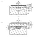
(実施例1の変形例1)
図8(a)は、実施例1の変形例1に係る弾性波デバイスの平面図、図8(b)は、共振領域付近の平面図、図8(c)および図8(d)は、図8(a)のA−A断面図である。図8(a)から図8(d)に示すように、分断領域62において上部電極16および上部圧電膜14bが除去されていてもよい。その他の構造は実施例1と同じであり説明を省略する。
(
8 (a) is a plan view of an acoustic wave device according to a first modification of the first embodiment, FIG. 8 (b) is a plan view in the vicinity of a resonance region, and FIGS. 8 (c) and 8 (d) are It is AA sectional drawing of Fig.8 (a). As shown in FIG. 8A to FIG. 8D, the
分断領域62における圧電膜14を全て除去すると、共振領域50を下部電極12で支持することなる。よって、下部電極12が破損されやすくなる。そこで、分断領域62の圧電膜14の一部を除去する。これにより、共振領域50間の弾性波の漏洩をより抑制できる。分断領域62に挿入膜28が設けられている。挿入膜28をストッパに分断領域62の上部電極16および上部圧電膜14bを除去することができる。これにより、圧電膜14の一部を制御よく除去できる。
When all of the
(実施例1の変形例2)
図9(a)は、実施例1の変形例2に係る弾性波デバイスの平面図、図9(b)は、共振領域付近の平面図、図9(c)および図9(d)は、図9(a)のA−A断面図である。図9(a)から図9(d)に示すように、分断領域62において下部電極12が分断され、圧電膜14および上部電極16は分断されていない。その他の構造は実施例1と同じであり説明を省略する。
(Modified Example 2 of Example 1)
9 (a) is a plan view of an acoustic wave device according to a second modification of the first embodiment, FIG. 9 (b) is a plan view around the resonance region, and FIGS. 9 (c) and 9 (d) are It is AA sectional drawing of Fig.9 (a). As shown in FIGS. 9A to 9D, the
実施例1およびその変形例2のように、分断領域62では、下部電極12および上部電極16のいずれか一方が分断され下部電極12および上部電極16の他方が分断されていなければよい。
As in the first embodiment and the second modification thereof, it is only necessary that one of the
(実施例1の変形例3)
図10(a)は、実施例1の変形例3に係る弾性波デバイスの平面図、図10(b)は、共振領域付近の平面図、図10(c)および図10(d)は、図10(a)のA−A断面図である。図10(a)から図10(d)に示すように、挿入膜28が設けられていない。その他の構造は実施例1と同じであり説明を省略する。
(
10 (a) is a plan view of an acoustic wave device according to a third modification of the first embodiment, FIG. 10 (b) is a plan view around the resonance region, and FIGS. 10 (c) and 10 (d) are It is AA sectional drawing of Fig.10 (a). As shown in FIGS. 10A to 10D, the
特許文献1のように、平面視において空隙内に複数の共振領域を設けるときに、空隙内に下部電極および上部電極のいずれも設けられていない領域が存在すると、圧電膜が機械的に破壊され易くなる。実施例1の変形例3によれば、平面視において下部電極12および上部電極16の少なくとも一方の電極が設けられた領域が空隙30の略全てと重なっている。これにより、下部電極12および上部電極16の少なくとも一方が圧電膜14を補強する。このため、積層膜18の機械的破損を抑制できる。
As in
(実施例1の変形例4)
図11(a)は、実施例1の変形例4に係る弾性波デバイスの平面図、図11(b)は、共振領域付近の平面図、図11(c)および図11(d)は、図11(a)のA−A断面図である。図11(a)から図11(d)に示すように、挿入膜28は分断領域62に設けられその他の領域には設けられていない。その他の構造は実施例1と同じであり説明を省略する。
(
11 (a) is a plan view of an acoustic wave device according to a fourth modification of the first embodiment, FIG. 11 (b) is a plan view around the resonance region, and FIGS. 11 (c) and 11 (d) are It is AA sectional drawing of Fig.11 (a). As shown in FIG. 11A to FIG. 11D, the
実施例1の変形例4のように、挿入膜28は、分断領域62以外に設けられていなくてもよい。挿入膜28が分断領域62に設けられていれば、共振領域50間の弾性波の漏洩70bを抑制することにより、Q値等の圧電薄膜共振器の特性の劣化を抑制できる。また、分断領域62における積層膜18の強度を大きくできる。
As in the fourth modification of the first embodiment, the
(実施例1の変形例5)
図12(a)は、実施例1の変形例5に係る弾性波デバイスの平面図、図12(b)は、共振領域付近の平面図である。図12(a)および図12(b)に示すように、空隙30の平面形状は円形状であり、共振領域50と分断領域62を合成した領域の平面形状は円形状である。その他の構造は実施例1と同じであり説明を省略する。
(Modification 5 of Embodiment 1)
12 (a) is a plan view of an acoustic wave device according to a fifth modification of the first embodiment, and FIG. 12 (b) is a plan view of the vicinity of the resonance region. As shown in FIGS. 12 (a) and 12 (b), the planar shape of the
(実施例1の変形例6)
図13(a)は、実施例1の変形例6に係る弾性波デバイスの平面図、図13(b)は、共振領域付近の平面図である。図13(a)および図13(b)に示すように、空隙30の平面形状は四角形状であり、共振領域50と分断領域62を合成した領域の平面形状は四角形状である。その他の構造は実施例1と同じであり説明を省略する。
(Modification 6 of Embodiment 1)
FIG. 13A is a plan view of an acoustic wave device according to a sixth modification of the first embodiment, and FIG. 13B is a plan view of the vicinity of the resonance region. As shown in FIGS. 13A and 13B, the planar shape of the
(実施例1の変形例7)
図14(a)は、実施例1の変形例7に係る弾性波デバイスの平面図、図14(b)は、共振領域付近の平面図である。図14(a)および図14(b)に示すように、空隙30の平面形状は五角形状であり、共振領域50と分断領域62を合成した領域の平面形状は五角形状である。その他の構造は実施例1と同じであり説明を省略する。
(
FIG. 14A is a plan view of an acoustic wave device according to a seventh modification of the first embodiment, and FIG. 14B is a plan view of the vicinity of the resonance region. As shown in FIGS. 14A and 14B, the planar shape of the
実施例1の変形例5から7のように、空隙30および共振領域50と分断領域62とを合成した領域の平面形状は円形状または多角形状でもよい。実施例1の変形例1から4においても空隙30および共振領域50と分断領域62とを合成した領域の平面形状は円形状または多角形状としてもよい。空隙30と、共振領域50と分断領域62とを合成した領域と、が相似形である例を説明したが、相似形でなくてもよい。
As in the fifth to seventh modifications of the first embodiment, the planar shape of the
(実施例1の変形例8)
図15(a)は、実施例1の変形例8に係る弾性波デバイスの平面図、図15(b)は、共振領域付近の平面図である。図15(a)および図15(b)に示すように、空隙30および共振領域50と分断領域62とを合成した領域の平面形状は楕円形状であり、分断領域62は短軸に沿って設けられていてもよい。その他の構造は実施例1と同じであり説明を省略する。楕円形状を2分割する場合、短軸で2分割すると、共振領域50の縦横比が1に近くなる。このため、スプリアスを抑制できる。
(
Fig.15 (a) is a top view of the elastic wave device based on the
(実施例1の変形例9)
図16(a)は、実施例1の変形例9に係る弾性波デバイスの平面図、図16(b)は、共振領域付近の平面図である。図16(a)および図16(b)に示すように、分断領域62と共振領域50との境界は波状である。分断領域62における挿入膜28の輪郭は波状である。その他の構造は実施例1と同じであり説明を省略する。分断領域62と共振領域50との境界を波状とすることでスプリアスを抑制できる。
(Modification 9 of Embodiment 1)
FIG. 16 (a) is a plan view of an elastic wave device according to a ninth modification of the first embodiment, and FIG. 16 (b) is a plan view around the resonance region. As shown in FIGS. 16 (a) and 16 (b), the boundary between the divided
(実施例1の変形例10)
図17(a)は、実施例1の変形例10に係る弾性波デバイスの平面図、図17(b)は、共振領域付近の平面図である。図17(a)および図17(b)に示すように、分断領域62は曲線状である。分断領域62に沿った挿入膜28は曲線状である。その他の構造は実施例1と同じであり説明を省略する。分断領域62を曲線状とすることで、スプリアスを抑制できる。また、空隙30の中心60が分断領域62に含まれない場合、中心60は挿入膜28と重ならなくてもよい。
(Modified Example 10 of Example 1)
FIG. 17A is a plan view of an elastic wave device according to a tenth modification of the first embodiment, and FIG. 17B is a plan view of the vicinity of the resonance region. As shown in FIGS. 17 (a) and 17 (b), the divided
(実施例1の変形例11)
図18(a)は、実施例1の変形例11に係る弾性波デバイスの平面図、図18(b)は、共振領域付近の平面図である。図18(a)および図18(b)に示すように、分断領域62は長軸および短軸から傾いている。分断領域62に沿った挿入膜28は長軸および短軸から傾いている。その他の構造は実施例1と同じであり説明を省略する。分断領域62を曲線状とすることで、スプリアスを抑制できる。
(Modification 11 of Embodiment 1)
FIG. 18A is a plan view of an acoustic wave device according to a modification 11 of the first embodiment, and FIG. 18B is a plan view of the vicinity of the resonance region. As shown in FIGS. 18 (a) and 18 (b), the dividing
実施例1の変形例8から11の分断領域62の形状を実施例1およびその変形例1から7に適用してもよい。
The shapes of the divided
(実施例1の変形例12)
実施例1の変形例12および13は、空隙の構成を変えた例である。図19(a)および図19(b)は、実施例1の変形例12および13における共振領域近傍の断面図である。図19(a)に示すように、基板10の上面に窪みが形成されている。下部電極12は、基板10上に平坦に形成されている。これにより、空隙30が、基板10の窪みに形成されている。空隙30は共振領域50を含むように形成されている。その他の構成は、実施例1と同じであり説明を省略する。空隙30は、基板10を貫通するように形成されていてもよい。なお、下部電極12の下面に絶縁膜が接して形成されていてもよい。すなわち、空隙30は、基板10と下部電極12に接する絶縁膜との間に形成されていてもよい。絶縁膜としては、例えば窒化アルミニウム膜を用いることができる。
(
(実施例1の変形例13)
図19(b)に示すように、共振領域50の下部電極12下に音響反射膜31が形成されている。音響反射膜31は、音響インピーダンスの低い膜31aと音響インピーダンスの高い膜31bとが交互に設けられている。膜31aおよび31bの膜厚は例えばそれぞれ略λ/4(λは弾性波の波長)である。膜31aと膜31bの積層数は任意に設定できる。例えば、音響反射膜31は、基板10中に音響インピーダンスの異なる膜が一層設けられている構成でもよい。その他の構成は、実施例1と同じであり説明を省略する。
(Modification 13 of Embodiment 1)
As shown in FIG. 19B, the
実施例1およびその変形例1から11において、実施例1の変形例12と同様に空隙30を形成してもよく、実施例1の変形例13と同様に空隙30の代わりに音響反射膜31を形成してもよい。
In the first embodiment and the first to eleventh modifications thereof, the
実施例1およびその変形例1から12のように、圧電薄膜共振器は、共振領域50において空隙30が基板10と下部電極12との間に形成されているFBAR(Film Bulk Acoustic Resonator)でもよい。また、実施例1の変形例13のように、圧電薄膜共振器は、共振領域50において下部電極12下に圧電膜14を伝搬する弾性波を反射する音響反射膜31を備えるSMR(Solidly Mounted Resonator)でもよい。このように、基板10内または上に設けられる音響反射層は、空隙30、または音響特性の異なる少なくとも2種類の層が積層された音響反射膜31を含めばよい。
As in the first embodiment and its first to twelfth modifications, the piezoelectric thin film resonator may be a film bulk acoustic resonator (FBAR) in which the
実施例2は、デュプレクサの例である。図20は、実施例2に係るデュプレクサの回路図である。図20に示すように、共通端子Antはアンテナ44に接続される。共通端子Antと送信端子Txとの間に送信フィルタ40が接続されている。共通端子Antと受信端子Rxとの間に受信フィルタ42が接続されている。共通端子Antとグランドとの間に整合回路としてインダクタL1が接続されている。送信フィルタ40は、送信端子Txから入力された信号のうち送信帯域の信号を送信信号として共通端子Antに通過させ、他の周波数の信号を抑圧する。受信フィルタ42は、共通端子Antから入力された信号のうち受信帯域の信号を受信信号として受信端子Rxに通過させ、他の周波数の信号を抑圧する。インダクタL1は、送信フィルタ40を通過した送信信号が受信フィルタ42に漏れず共通端子Antから出力されるようにインピーダンスを整合させる。
Example 2 is an example of a duplexer. FIG. 20 is a circuit diagram of the duplexer according to the second embodiment. As shown in FIG. 20, the common terminal Ant is connected to the
送信フィルタ40は、ラダー型フィルタである。共通端子Antと送信端子Txとの間に1または複数の直列共振器S1からS4が直列に接続されている。共通端子Antと送信端子Txとの間に1または複数の並列共振器P1からP3が並列に接続されている。並列共振器P1からP3の一端は共通にインダクタL2を介し接地されている。並列共振器P1は共振器P1aおよびP1bに直列に分割されている。
The
図21(a)は、実施例2における送信フィルタの平面図、図21(b)は、空隙の平面図である。図21(a)に示すように、基板10上に直列共振器S1からS4、並列共振器P1からP3、配線45および端子46が形成されている。直列共振器S1からS4、および並列共振器P1からP3は共振領域50を有する。配線45は共振領域50同士を接続、および共振領域50と端子46とを接続する、端子46は入力端子Tin、出力端子Toutおよびグランド端子Tgを含む。配線45および端子46は、下部電極12または上部電極16により形成されている。
Fig.21 (a) is a top view of the transmission filter in Example 2, FIG.21 (b) is a top view of a space | gap. As shown in FIG. 21A, series resonators S1 to S4, parallel resonators P1 to P3, a
図21(a)および図21(b)に示すように、並列共振器P1以外の共振器は、単一の空隙30に単一の共振領域50が設けられている。共振器P1aおよびP1bは実施例1およびその変形例に係る圧電薄膜共振器であり、単一の空隙30aに2つの共振領域50と分断領域62が設けられている。共振器P1aおよびP1bが設けられた空隙30aと他の空隙30とは楕円形状を有している。このように、空隙30aと30とが同様の形状であるため、空隙30aおよび30上に積層膜18を形成する応力条件をほぼ同一にできる。よって、空隙30aおよび30と積層膜18とを容易に形成することができる。
As shown in FIGS. 21 (a) and 21 (b), the resonators other than the parallel resonator P1 are provided with a
実施例2のように、送信フィルタ40は、実施例1およびその変形例の単一の空隙30に設けられた複数の共振領域50にそれぞれ対応する複数の圧電薄膜共振器を含む。これにより、共振器P1aとP1bとの間の配線の寄生容量C0を小さくできる。よって、2次歪を抑制できる。また、積層膜の機械的な破壊を抑制できる。
As in the second embodiment, the
実施例2では、送信フィルタ40に実施例1およびその変形例を用いる例を説明したが、受信フィルタ42に実施例1およびその変形例を用いてもよい。また、ラダー型フィルタに実施例1およびその変形例を用いる例を説明したがラティス型フィルタまたは多重モードフィルタでもよい。マルチプレクサの例としてデュプレクサを説明したが。マルチプレクサはトリプレクサまたはクワッドプレクサでもよい。
In the second embodiment, an example using the first embodiment and its modification as the
また、並列共振器P1が複数の共振器P1aおよびP1b(分割共振器)に分割されており、共振器P1aおよびP1bに対応する複数の共振領域50は空隙30aに共通に設けられている。これにより、2次歪を抑制できる。分割される共振器は、1または複数の直列共振器および1または複数の並列共振器の少なくとも1つの共振器であればよい。2次歪を抑制する観点から出力端子に最も近い直列共振器S1および/または並列共振器P1が分割されていることが好ましい。
分割は、図2(b)のような並列分割でもよい。直列共振器および並列共振器の数は任意に設定できる。
The parallel resonator P1 is divided into a plurality of resonators P1a and P1b (split resonators), and a plurality of
The division may be parallel division as shown in FIG. 2 (b). The number of series resonators and parallel resonators can be set arbitrarily.
実施例3は、ラダー型フィルタに実施例1およびその変形例を用いる例である。図22(a)は、実施例3および比較例2に係るフィルタの回路図、図22(b)は、比較例2に係るフィルタの平面図である。 The third embodiment is an example using the first embodiment and its modification for the ladder type filter. 22 (a) is a circuit diagram of a filter according to Example 3 and Comparative Example 2, and FIG. 22 (b) is a plan view of a filter according to Comparative Example 2. FIG.
図22(a)に示すように、入力端子Tinと出力端子Toutとの間に直列に直列共振器S1およびS2が接続され、並列に並列共振器P1が接続されている。図22(b)に示すように、基板10上に共振領域50、配線45および端子46が設けられている。配線45および端子46は下部電極12または上部電極16により形成されている。比較例2においては、基板10上に共振器に対応する3つの共振領域50が形成されている。3つの共振領域50はそれぞれ単一の空隙30上に設けられている。
As shown in FIG. 22A, series resonators S1 and S2 are connected in series between the input terminal Tin and the output terminal Tout, and a parallel resonator P1 is connected in parallel. As shown in FIG. 22B, the
図23は、実施例3に係るフィルタの平面図である。図23に示すように、実施例3では、直列共振器S1およびS2に対応する共振領域50は空隙30に共通に設けられている。直列共振器S1およびS2の上部電極16は分断領域62で分断されている。直列共振器S1およびS2の上部電極16は共通に並列共振器P1に接続されている。
FIG. 23 is a plan view of the filter according to the third embodiment. As shown in FIG. 23, in the third embodiment, the
実施例3のように、複数の直列共振器S1およびS2は単一の空隙30を共有する実施例1およびその変形例でもよい。
As in the third embodiment, the plurality of series resonators S1 and S2 may share the
図24(a)は、実施例3の変形例1に係るフィルタの平面図、図24(b)は、共振領域付近の平面図である。図24(a)および図24(b)に示すように、空隙30に共通に直列共振器S1およびS2並びに並列共振器P1に対応する3つの共振領域50が設けられている。上部電極16は分断領域62で分断されている。下部電極12は分断領域62に設けられている。3つの共振器は下部電極12により電気的に接続されている。その他の構成は実施例3と同じであり説明を省略する。
Fig.24 (a) is a top view of the filter based on the
図25(a)は、実施例3の変形例2に係るフィルタの回路図、図25(b)は、平面図、図25(c)は、共振領域付近の平面図である。図25(a)に示すように、直列共振器S1とS2との間のノードとグランドと間に2つの並列共振器P1およびP2が並列に接続されている。図25(b)および図25(c)に示すように、空隙30に共通に直列共振器S1およびS2並びに並列共振器P1およびP2に対応する4つの共振領域50が設けられている。上部電極16は分断領域62で分断されている。下部電極12は分断領域62に設けられている。4つの共振器は下部電極12により電気的に接続されている。その他の構成は実施例3と同じであり説明を省略する。
FIG. 25 (a) is a circuit diagram of a filter according to a second modification of the third embodiment, FIG. 25 (b) is a plan view, and FIG. 25 (c) is a plan view around the resonance region. As shown in FIG. 25 (a), two parallel resonators P1 and P2 are connected in parallel between the node between the series resonators S1 and S2 and the ground. As shown in FIGS. 25B and 25C, four
実施例3の変形例1および2のように、複数の直列共振器S1およびS2並びに並列共振器P1、P2は単一の空隙30を共有する実施例1およびその変形例でもよい。
As in the first and second modifications of the third embodiment, the plurality of series resonators S1 and S2 and the parallel resonators P1 and P2 may share the
実施例3の変形例のように、1または複数の直列共振器の少なくとも1つと1または複数の並列共振器の少なくとも1つに対応する共振領域50が空隙30に共通に設けられている。これにより、直列共振器と並列共振器との間の配線の寄生容量を抑制できる。また、積層膜の機械的な破壊を抑制できる。
As in the modification of the third embodiment, the
以上、本発明の実施例について詳述したが、本発明はかかる特定の実施例に限定されるものではなく、特許請求の範囲に記載された本発明の要旨の範囲内において、種々の変形・変更が可能である。 As mentioned above, although the embodiment of the present invention has been described in detail, the present invention is not limited to such a specific embodiment, and various modifications may be made within the scope of the subject matter of the present invention described in the claims. Changes are possible.
10 基板
12 下部電極
14 圧電膜
16 上部電極
18 積層膜
28 挿入膜
30 空隙
50 共振領域
52 外周領域
54 中央領域
60 空隙の中心
62 分断領域
Claims (12)
前記基板内または上に設けられた空隙である音響反射層と、
前記基板および前記音響反射層上に設けられた圧電膜と、
複数の共振領域が平面視において前記音響反射層内に共通に設けられるように、下部電極および上部電極のいずれか一方が分断され前記下部電極および前記上部電極の他方は分断されず、前記基板および前記音響反射層上に前記圧電膜を挟むように設けられた下部電極および上部電極と、
前記下部電極と前記上部電極との間に設けられ、平面視において前記複数の共振領域の各々の外周領域において少なくとも一部に設けられ、前記複数の共振領域の各々の中央領域には設けられていない挿入膜と、
を具備し、
前記複数の共振領域は各々前記圧電膜の少なくとも一部を挟み前記下部電極と前記上部電極とが対向する領域であり、
前記挿入膜は平面視において前記下部電極および前記上部電極のいずれか一方が分断された分断領域に重なり、前記分断領域は平面視において前記音響反射層と重なる弾性波デバイス。 A substrate,
An acoustic reflection layer which is an air gap provided in or on the substrate;
A piezoelectric film provided on the substrate and the acoustic reflection layer;
One of the lower electrode and the upper electrode is divided and the other of the lower electrode and the upper electrode is not divided so that a plurality of resonance regions are commonly provided in the acoustic reflection layer in plan view. A lower electrode and an upper electrode provided on the acoustic reflection layer so as to sandwich the piezoelectric film;
It is provided between the lower electrode and the upper electrode, provided at least in part in the outer peripheral area of each of the plurality of resonance areas in plan view, and provided in the central area of each of the plurality of resonance areas. There is no insertion membrane,
Equipped with
The plurality of resonance regions are regions in which the lower electrode and the upper electrode face each other with at least a portion of the piezoelectric film interposed therebetween,
The elastic wave device, wherein the insertion film overlaps a divided area in which any one of the lower electrode and the upper electrode is divided in a plan view, and the divided area overlaps the acoustic reflection layer in a plan view .
前記挿入膜は前記下部圧電膜と前記上部圧電膜との間に設けられ、
前記分断領域において、前記上部電極および前記上部圧電膜が分断されている請求項7記載の弾性波デバイス。 The piezoelectric film includes a lower piezoelectric film and an upper piezoelectric film provided on the lower piezoelectric film.
The insertion film is provided between the lower piezoelectric film and the upper piezoelectric film.
The elastic wave device according to claim 7, wherein the upper electrode and the upper piezoelectric film are separated in the divided region.
前記入力端子と前記出力端子との間に並列に接続された1または複数の並列共振器と、
を具備し、
前記1または複数の直列共振器および前記1または複数の並列共振器の少なくとも1つは複数の分割共振器に分割されており、
前記複数の共振領域はそれぞれ前記複数の分割共振器に対応する請求項10記載の弾性波デバイス。 One or more series resonators connected in series between the input terminal and the output terminal;
One or more parallel resonators connected in parallel between the input terminal and the output terminal;
Equipped with
At least one of the one or more series resonators and the one or more parallel resonators is divided into a plurality of divided resonators,
The elastic wave device according to claim 10, wherein the plurality of resonance regions correspond to the plurality of divided resonators, respectively.
前記入力端子と前記出力端子との間に並列に接続された1または複数の並列共振器と、
を具備し、
前記複数の共振領域は、前記1または複数の直列共振器の少なくとも1つと前記1または複数の並列共振器の少なくとも1つを含む請求項10記載の弾性波デバイス。 One or more series resonators connected in series between the input terminal and the output terminal;
One or more parallel resonators connected in parallel between the input terminal and the output terminal;
Equipped with
The elastic wave device according to claim 10, wherein the plurality of resonance regions include at least one of the one or more series resonators and at least one of the one or more parallel resonators.
Priority Applications (2)
| Application Number | Priority Date | Filing Date | Title |
|---|---|---|---|
| JP2016129230A JP6538007B2 (en) | 2016-06-29 | 2016-06-29 | Elastic wave device |
| US15/623,307 US10666220B2 (en) | 2016-06-29 | 2017-06-14 | Acoustic wave device |
Applications Claiming Priority (1)
| Application Number | Priority Date | Filing Date | Title |
|---|---|---|---|
| JP2016129230A JP6538007B2 (en) | 2016-06-29 | 2016-06-29 | Elastic wave device |
Publications (3)
| Publication Number | Publication Date |
|---|---|
| JP2018006919A JP2018006919A (en) | 2018-01-11 |
| JP2018006919A5 JP2018006919A5 (en) | 2018-03-22 |
| JP6538007B2 true JP6538007B2 (en) | 2019-07-03 |
Family
ID=60808019
Family Applications (1)
| Application Number | Title | Priority Date | Filing Date |
|---|---|---|---|
| JP2016129230A Active JP6538007B2 (en) | 2016-06-29 | 2016-06-29 | Elastic wave device |
Country Status (2)
| Country | Link |
|---|---|
| US (1) | US10666220B2 (en) |
| JP (1) | JP6538007B2 (en) |
Families Citing this family (7)
| Publication number | Priority date | Publication date | Assignee | Title |
|---|---|---|---|---|
| WO2018063294A1 (en) * | 2016-09-30 | 2018-04-05 | Intel Corporation | Film bulk acoustic resonator (fbar) devices for high frequency rf filters |
| JP2019193220A (en) * | 2018-04-27 | 2019-10-31 | サムソン エレクトロ−メカニックス カンパニーリミテッド. | Filter including bulk acoustic wave resonator |
| JP2020088578A (en) * | 2018-11-22 | 2020-06-04 | 太陽誘電株式会社 | Acoustic wave device, filter, and multiplexer |
| JP7290941B2 (en) * | 2018-12-27 | 2023-06-14 | 太陽誘電株式会社 | Acoustic wave devices, filters and multiplexers |
| JP7344011B2 (en) | 2019-06-04 | 2023-09-13 | 太陽誘電株式会社 | Piezoelectric thin film resonators, filters and multiplexers |
| US11165410B2 (en) * | 2019-10-01 | 2021-11-02 | Avago Technologies International Sales Pte. Limited | Bulk acoustic wave resonator |
| WO2022211056A1 (en) * | 2021-03-31 | 2022-10-06 | 株式会社村田製作所 | Elastic wave device |
Family Cites Families (14)
| Publication number | Priority date | Publication date | Assignee | Title |
|---|---|---|---|---|
| US6262637B1 (en) * | 1999-06-02 | 2001-07-17 | Agilent Technologies, Inc. | Duplexer incorporating thin-film bulk acoustic resonators (FBARs) |
| JP4478910B2 (en) * | 2001-05-11 | 2010-06-09 | 宇部興産株式会社 | Piezoelectric thin film resonator |
| JP4622574B2 (en) | 2005-02-21 | 2011-02-02 | 株式会社デンソー | Ultrasonic element |
| US7868522B2 (en) * | 2005-09-09 | 2011-01-11 | Avago Technologies Wireless Ip (Singapore) Pte. Ltd. | Adjusted frequency temperature coefficient resonator |
| JP4218672B2 (en) * | 2005-10-21 | 2009-02-04 | 株式会社村田製作所 | Piezoelectric resonator, piezoelectric filter, communication device |
| JP5036435B2 (en) | 2006-09-01 | 2012-09-26 | 太陽誘電株式会社 | Elastic wave device, filter and duplexer |
| JP2008131194A (en) * | 2006-11-17 | 2008-06-05 | Toshiba Corp | Thin film piezoelectric resonator |
| JP2008211394A (en) * | 2007-02-23 | 2008-09-11 | Matsushita Electric Works Ltd | Resonator |
| US7548140B2 (en) | 2007-04-16 | 2009-06-16 | Avago Technologies General Ip (Singapore) Pte. Ltd. | Bulk acoustic wave (BAW) filter having reduced second harmonic generation and method of reducing second harmonic generation in a BAW filter |
| JP5200716B2 (en) * | 2008-07-14 | 2013-06-05 | 株式会社村田製作所 | Duplexer |
| JP5161698B2 (en) * | 2008-08-08 | 2013-03-13 | 太陽誘電株式会社 | Piezoelectric thin film resonator and filter or duplexer using the same |
| JP5792554B2 (en) | 2011-08-09 | 2015-10-14 | 太陽誘電株式会社 | Elastic wave device |
| JP6336712B2 (en) * | 2013-01-28 | 2018-06-06 | 太陽誘電株式会社 | Piezoelectric thin film resonator, filter and duplexer |
| JP6371518B2 (en) * | 2013-12-17 | 2018-08-08 | 太陽誘電株式会社 | Piezoelectric thin film resonator, method for manufacturing the same, filter, and duplexer |
-
2016
- 2016-06-29 JP JP2016129230A patent/JP6538007B2/en active Active
-
2017
- 2017-06-14 US US15/623,307 patent/US10666220B2/en active Active
Also Published As
| Publication number | Publication date |
|---|---|
| US20180006631A1 (en) | 2018-01-04 |
| JP2018006919A (en) | 2018-01-11 |
| US10666220B2 (en) | 2020-05-26 |
Similar Documents
| Publication | Publication Date | Title |
|---|---|---|
| JP6538007B2 (en) | Elastic wave device | |
| US10790799B2 (en) | Piezoelectric thin film resonator, filter, and multiplexer | |
| JP6661521B2 (en) | Filters and multiplexers | |
| JP6556099B2 (en) | Piezoelectric thin film resonator, filter and multiplexer | |
| JP5792554B2 (en) | Elastic wave device | |
| US10910547B2 (en) | Piezoelectric thin film resonator, filter, and multiplexer | |
| JP2015139167A (en) | Piezoelectric thin film resonator, filter, and duplexer | |
| JP2017126900A (en) | Piezoelectric thin film resonator, filter, and duplexer | |
| JP6515042B2 (en) | Elastic wave device | |
| JP6423782B2 (en) | Piezoelectric thin film resonator and filter | |
| JP2019075736A (en) | Ladder filter, piezoelectric thin film resonator and manufacturing method thereof | |
| US9787282B2 (en) | Piezoelectric thin film resonator, filter and duplexer | |
| US10862448B2 (en) | Piezoelectric thin film resonator, filter, and multiplexer | |
| JP6556173B2 (en) | Piezoelectric thin film resonator, filter and multiplexer | |
| JP2019009671A (en) | Piezoelectric thin film resonator, filter, and multiplexer | |
| JP7456737B2 (en) | Piezoelectric thin film resonators, filters and multiplexers | |
| US10680576B2 (en) | Piezoelectric thin film resonator, filter, and duplexer | |
| JP2017112437A (en) | Piezoelectric thin film resonator, filter, and duplexer | |
| JP5931490B2 (en) | Elastic wave device | |
| JP7344011B2 (en) | Piezoelectric thin film resonators, filters and multiplexers | |
| JP2019212982A (en) | Piezoelectric thin film resonator, filter, and multiplexer | |
| JP6909059B2 (en) | Piezoelectric thin film resonators, filters and multiplexers | |
| JP7383404B2 (en) | Piezoelectric thin film resonators, filters and multiplexers | |
| JP7302981B2 (en) | Filters and multiplexers | |
| JP7438674B2 (en) | Piezoelectric thin film resonators, filters and multiplexers |
Legal Events
| Date | Code | Title | Description |
|---|---|---|---|
| A521 | Request for written amendment filed |
Free format text: JAPANESE INTERMEDIATE CODE: A523 Effective date: 20180207 |
|
| A621 | Written request for application examination |
Free format text: JAPANESE INTERMEDIATE CODE: A621 Effective date: 20180207 |
|
| A977 | Report on retrieval |
Free format text: JAPANESE INTERMEDIATE CODE: A971007 Effective date: 20181203 |
|
| A131 | Notification of reasons for refusal |
Free format text: JAPANESE INTERMEDIATE CODE: A131 Effective date: 20181218 |
|
| A521 | Request for written amendment filed |
Free format text: JAPANESE INTERMEDIATE CODE: A523 Effective date: 20190215 |
|
| TRDD | Decision of grant or rejection written | ||
| A01 | Written decision to grant a patent or to grant a registration (utility model) |
Free format text: JAPANESE INTERMEDIATE CODE: A01 Effective date: 20190528 |
|
| A61 | First payment of annual fees (during grant procedure) |
Free format text: JAPANESE INTERMEDIATE CODE: A61 Effective date: 20190605 |
|
| R150 | Certificate of patent or registration of utility model |
Ref document number: 6538007 Country of ref document: JP Free format text: JAPANESE INTERMEDIATE CODE: R150 |
|
| R250 | Receipt of annual fees |
Free format text: JAPANESE INTERMEDIATE CODE: R250 |
|
| R250 | Receipt of annual fees |
Free format text: JAPANESE INTERMEDIATE CODE: R250 |