JP6531695B2 - Power supply system - Google Patents
Power supply system Download PDFInfo
- Publication number
- JP6531695B2 JP6531695B2 JP2016071660A JP2016071660A JP6531695B2 JP 6531695 B2 JP6531695 B2 JP 6531695B2 JP 2016071660 A JP2016071660 A JP 2016071660A JP 2016071660 A JP2016071660 A JP 2016071660A JP 6531695 B2 JP6531695 B2 JP 6531695B2
- Authority
- JP
- Japan
- Prior art keywords
- power supply
- voltage
- mosfets
- circuit
- supply line
- Prior art date
- Legal status (The legal status is an assumption and is not a legal conclusion. Google has not performed a legal analysis and makes no representation as to the accuracy of the status listed.)
- Active
Links
Images


Classifications
-
- H—ELECTRICITY
- H02—GENERATION; CONVERSION OR DISTRIBUTION OF ELECTRIC POWER
- H02J—CIRCUIT ARRANGEMENTS OR SYSTEMS FOR SUPPLYING OR DISTRIBUTING ELECTRIC POWER; SYSTEMS FOR STORING ELECTRIC ENERGY
- H02J1/00—Circuit arrangements for dc mains or dc distribution networks
-
- B—PERFORMING OPERATIONS; TRANSPORTING
- B60—VEHICLES IN GENERAL
- B60R—VEHICLES, VEHICLE FITTINGS, OR VEHICLE PARTS, NOT OTHERWISE PROVIDED FOR
- B60R16/00—Electric or fluid circuits specially adapted for vehicles and not otherwise provided for; Arrangement of elements of electric or fluid circuits specially adapted for vehicles and not otherwise provided for
- B60R16/02—Electric or fluid circuits specially adapted for vehicles and not otherwise provided for; Arrangement of elements of electric or fluid circuits specially adapted for vehicles and not otherwise provided for electric constitutive elements
- B60R16/03—Electric or fluid circuits specially adapted for vehicles and not otherwise provided for; Arrangement of elements of electric or fluid circuits specially adapted for vehicles and not otherwise provided for electric constitutive elements for supply of electrical power to vehicle subsystems or for
- B60R16/033—Electric or fluid circuits specially adapted for vehicles and not otherwise provided for; Arrangement of elements of electric or fluid circuits specially adapted for vehicles and not otherwise provided for electric constitutive elements for supply of electrical power to vehicle subsystems or for characterised by the use of electrical cells or batteries
-
- H—ELECTRICITY
- H02—GENERATION; CONVERSION OR DISTRIBUTION OF ELECTRIC POWER
- H02J—CIRCUIT ARRANGEMENTS OR SYSTEMS FOR SUPPLYING OR DISTRIBUTING ELECTRIC POWER; SYSTEMS FOR STORING ELECTRIC ENERGY
- H02J7/00—Circuit arrangements for charging or depolarising batteries or for supplying loads from batteries
- H02J7/0068—Battery or charger load switching, e.g. concurrent charging and load supply
Description
本発明は、メイン電源供給ライン及びサブ電源供給ラインを通じて電源供給する電源システムに関する。 The present invention relates to a power supply system that supplies power through a main power supply line and a sub power supply line.
例えば、車両(例えば自動車)には多くの電子制御装置(ECU:ElectoronicControlUnit)が搭載されており、これらの電子制御装置が連携動作することで各種制御が行われる。これらの電子制御装置は、バッテリ電源から分岐された電源ラインを通じて電源供給される。これらの電子制御装置の中には、動作安全性を高めるため、メイン電源となるバッテリ電源又はそのメイン電源の供給ラインにたとえ異常等を生じたとしても、その他のサブ電源(例えば補助バッテリ)をサブ電源供給ラインを通じて電源供給することで動作を維持しなければならないものがある。この場合、メイン電源供給ライン及びサブ電源供給ラインからダイオードOR回路を通じて1つの電子制御装置に電源供給できる(例えば、特許文献1参照)。このような技術を用いることで、サブ電源供給ラインからメイン電源供給ラインへの逆流防止を図ることができる。 For example, many electronic control units (ECUs: Electoronic Control Units) are mounted on a vehicle (for example, an automobile), and various controls are performed by cooperative operation of these electronic control units. These electronic control units are supplied with power through a power supply line branched from the battery power supply. Among these electronic control devices, in order to enhance the operation safety, even if an abnormality or the like occurs in the battery power source serving as the main power source or the supply line of the main power source, other sub power sources (for example, auxiliary batteries) There are some which must maintain operation by supplying power through the sub power supply line. In this case, power can be supplied to one electronic control unit from the main power supply line and the sub power supply line through the diode OR circuit (see, for example, Patent Document 1). By using such a technique, it is possible to prevent backflow from the sub power supply line to the main power supply line.
しかし、メイン電源供給ライン及びサブ電源供給ラインからダイオードOR回路を通じて1つの電子制御装置に電源供給すると、複数のダイオードの順方向電圧の設計値を同一値に設定した場合であっても当該順方向電圧に製造ばらつきを生じている場合には、何れのダイオードを通じて電源供給されるか不明となる。したがって、ダイオードOR回路を用いたときには、メイン電源供給ライン、サブ電源供給ラインの何れのラインに全供給電流が流れてもいいように、各種の回路を構成しなければならず、サブ電源の構成回路の不必要な大型化の懸念がある。特許文献1ではメイン電源電圧とサブ電源電圧を調整することでこの問題の解決を図っている。
However, when power is supplied to one electronic control unit from the main power supply line and the sub power supply line through the diode OR circuit, even if the design values of the forward voltages of the plurality of diodes are set to the same value, the forward direction If there are manufacturing variations in the voltage, it becomes unclear which diode is used to supply power. Therefore, when a diode OR circuit is used, various circuits must be configured to allow all the supply current to flow through either the main power supply line or the sub power supply line, and the configuration of the sub power supply There is a concern about unnecessary enlargement of the circuit. In
しかし、特許文献1のように逆流防止用にダイオードOR回路が用いられると、順方向電圧の電圧降下分が大きくなり低電圧動作には不向きである。そのため、ダイオードORを用いたまま低電圧動作させるためには、低電圧入力を許容可能な昇圧/昇降圧電源回路等、比較的高価な電源回路を用いて内部電源回路を構成しなければならなくなり好ましくない。
However, when a diode OR circuit is used for backflow prevention as in
本発明は、上記事情に鑑みてなされたもので、その目的は、メイン電源供給ラインからのメイン電源の入力電圧が低電圧であったとしても供給するメイン電源の電圧を極力高く保持できるようにすると共に、メイン電源供給ラインを通じて電源供給できなくてもサブ電源供給ラインから信頼性良く電源供給できるようにした電源システムを提供することにある。 The present invention has been made in view of the above circumstances, and an object thereof is to maintain the voltage of the main power supply supplied as high as possible even if the input voltage of the main power supply from the main power supply line is a low voltage. It is another object of the present invention to provide a power supply system capable of reliably supplying power from the sub power supply line even if power can not be supplied through the main power supply line.
請求項1記載の発明は、メイン電源供給ラインから入力されるメイン電源、及び、サブ電源供給ラインから入力されるサブ電源を1つの共通接続ノードを通じて供給する電源システムを対象としている。逆流防止回路は、MOSFET及びオンオフ制御部を備えている。オンオフ制御部がMOSFETのゲートにオン制御電圧を印加したときにはメイン電源供給ラインから入力されるメイン電源をMOSFETを通じて共通接続ノードに出力する。オンオフ制御部がMOSFETのゲートにオフ制御電圧を印加したときにはメイン電源供給ラインと共通接続ノードとの間の電気的接続を遮断することで逆流防止する。
The invention according to
他方、ダイオードはサブ電源供給ラインから共通接続ノードに向けて順方向電流が流れその逆流を防止するように接続されている。このため、メイン電源がメイン電源供給ラインを通じて電源供給されなくても、サブ電源がサブ電源供給ラインから共通接続ノードを通じて供給される。 On the other hand, the diodes are connected such that forward current flows from the sub power supply line toward the common connection node to prevent backflow. Therefore, even if the main power is not supplied through the main power supply line, the sub power is supplied from the sub power supply line through the common connection node.
しかも、オンオフ制御部がMOSFETのゲートにオン制御電圧を印加したときのメイン電源供給ラインから共通接続ノードへのメイン電源の降下電圧は、サブ電源供給ラインから共通接続ノードへのダイオードによるサブ電源電圧の降下電圧よりも低く設定されている。このため、メイン電源供給ラインから入力されるメイン電源の入力電圧がたとえ低電圧であったとしても、共通接続ノードを通じて供給されるメイン電源の電圧を極力高く保持できる。また、通常時にはメイン電源供給ラインから電流を流すことができ、サブ電源供給ラインを通じて流れる電流を制限でき、サブ電源の構成回路の不必要な大型化を防ぐことができる。 Moreover, when the on / off control unit applies the on control voltage to the gate of the MOSFET, the voltage drop of the main power supply from the main power supply line to the common connection node is the sub power supply voltage by the diode from the sub power supply line to the common connection node It is set lower than the voltage drop of. Therefore, even if the input voltage of the main power supply input from the main power supply line is a low voltage, the voltage of the main power supply supplied through the common connection node can be maintained as high as possible. In addition, in normal times, current can flow from the main power supply line, current flowing through the sub power supply line can be limited, and unnecessary enlargement of the sub power supply configuration circuit can be prevented.
以下、電源システムの幾つかの実施形態について図面を参照しながら説明する。以下に説明する各実施形態において、同一又は類似の動作を行う構成については、同一又は類似の符号を付して必要に応じて説明を省略する。なお、下記の実施形態において、同一又は類似する構成には、符号の十の位と一の位とに同一符号を付して説明を行っている。 Hereinafter, some embodiments of the power supply system will be described with reference to the drawings. In each embodiment described below, the same or similar reference numerals are assigned to components performing the same or similar operations, and the description will be omitted as necessary. In the following embodiments, the same or similar configurations are described by attaching the same reference numerals to the tens and ones places of the reference numerals.
(第1実施形態)
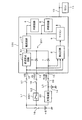
図1から図3は第1実施形態の説明図を示している。図1は統合型の電子制御装置(以下、統合ECUと称す:ECUはElectronic Control Unit)の電気的構成とその周辺の構成を示している。この統合ECU101は、逆流防止回路2、電源回路3、内部回路4、5、ダイオード6、7、検出回路8、及び、マイコン9を備える。電源システムSY1は、逆流防止回路2、ダイオード6、7を備え、電源回路3を後段に接続して構成される。
First Embodiment
1 to 3 show an explanatory view of the first embodiment. FIG. 1 shows the electrical configuration of an integrated electronic control unit (hereinafter referred to as an integrated ECU: ECU is an Electronic Control Unit) and the configuration around it. The integrated
内部回路4、5は、統合ECU101の機能の一部を示し、動作回路として構成される。例えば、内部回路4は、車両走行制御に法律上で必要な機能(例えばメータ制御機能)、又は、車両内の安全性に関係し事故の発生を未然に防いだり又は車両故障が発生したときに重要な動作(例えばエアバック制御)する機能(以下、必要に応じて走行系/安全系機能と称す)を示す。また、内部回路5は、ナビゲーションECU、オーディオECUなどの情報系機能を備える機能(以下、必要に応じて一般機能と称す)を示している。
The
この統合ECU101は、CAN又はLINなどの車内ネットワーク10に接続されている。マイコン9は、例えばCPU、ROM、RAM、バックアップRAM、EEPROM、I/O、及び、A/D変換回路(何れも図示せず)を備え、動作回路、制御部として構成される。マイコン9は、電源回路3から電源供給されていれば、統合ECU101自身に接続されたセンサ(図示せず)から各種情報(例えば、アクセル操作情報、ステアリング操作情報、ブレーキ操作情報、車速情報、車両ドア開閉情報等)を取得可能になっている。これらの情報は、車内ネットワーク10に接続された他のECU11に接続されたセンサ等から取得するように構成しても良い。
The integrated
統合ECU101は、メイン電源となるバッテリ電源+Bの電圧VBの入力端子12、サブ電源となるイグニッション電源IGの電圧VIGの入力端子13、及び、サブ電源となる補助バッテリ14の電圧VSUBの入力端子15、を備える。
The integrated
バッテリ電源+Bにはメインのヒューズ16が接続されており、バッテリ電源+Bはこのヒューズ16を通じてメイン電源供給ラインL1に接続されている。このメイン電源供給ラインL1と入力端子12との間にはヒューズ17が接続されており、入力端子12にはバッテリ電源+Bの電圧VBがヒューズ17を通じて印加されている。バッテリ電源+Bの電圧VBは、キースイッチSW1のオン/オフ状態に拘わらず入力端子12に入力される電源である。
The
統合ECU101の外部において、入力端子13はヒューズ18を介してサブ電源供給ラインL2に接続されている。メイン電源供給ラインL1とサブ電源供給ラインL2との間にはキースイッチSW1が接続されており、入力端子13には電圧VIGがキースイッチSW1及びヒューズ18を通じて印加される。この印加電圧VIGの電源をイグニッション電源IGと称す。なお、図示していないが、キースイッチSW1は例えばOFF、ACC、ON、STARTの各状態にユーザ操作可能になっており、このキースイッチSW1のスタータ制御信号(ON及びSTART時オン、OFF及びACC時オフ)は統合ECU101のマイコン9に入力されている。このイグニッション電源IGは、キースイッチSW1がON又はSTARTの位置で出力される電源である。すなわち車両ユーザによりキースイッチSW1が操作されると、イグニッション電源IGがオン/オフ通電される。
Outside the integrated ECU 101, the
また、入力端子15はヒューズ19を介してサブ電源供給ラインL3に接続されている。このサブ電源供給ラインL3には補助バッテリ14が接続されている。メイン電源供給ラインL1とサブ電源供給ラインL3との間には充電装置20が接続されており、充電装置20はバッテリ電源+Bの電圧を用いて補助バッテリ14に充電する。補助バッテリ14は、ヒューズ19を通じて入力端子15に動作補助用の電圧VSUBを供給する。この印加電圧を特に充電電源SUBと称す。この充電電源SUBは、キースイッチSW1のオン/オフ状態に拘わらず、補助バッテリ14に電圧が充電されていれば入力端子15に供給される電源である。
Further, the
入力端子13と電源回路3の入力ノードN1との間にはダイオード6が接続されている。このダイオード6は、入力端子13の側をアノードとすると共に電源回路3の入力ノードN1の側をカソードとして接続されている。また、入力端子15と電源回路3の入力ノードN1との間にもダイオード7が接続されている。このダイオード7は、入力端子15の側をアノードとすると共に電源回路3の入力ノードN1の側をカソードとして接続されている。
A
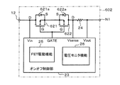
入力端子12と電源回路3の入力ノードN1との間には逆流防止回路2が接続されている。図2に逆流防止回路2の構成例を示すように、この逆流防止回路2はMOSFET21、22とオンオフ制御部23とを用いて構成されている。この逆流防止回路2は、図2に示すように、例えばゲートGが互いに共通接続された2つのNチャネル型のMOSFET21、22を備え、これらのMOSFET21、22からノードN1に流れる電流を検出する検出抵抗24を接続して構成される。2つのMOSFET21、22は、ソース同士が接続されると共に逆極性の状態で入力端子12とノードN1との間に直列接続されている。ノードN1は、ダイオード6、7のカソードと逆流防止回路2の出力とに共通接続される共通接続ノードとされている。
A
図2に示す構成例を詳細に説明する。逆流防止回路2は、入力端子12とノードN1との間にMOSFET21のドレインD、ソースS、MOSFET22のソースS、ドレインD、及び、検出抵抗24を直列接続して構成される。これらのMOSFET21、22は、それぞれ、内部半導体構造上においてソースSからドレインDに向けて順方向に寄生ダイオード21a、22aを備えるが、このように逆極性で接続しているのは、MOSFET21、22の寄生ダイオード21a、22aを互いに逆方向とし両寄生ダイオード21a、22aを通じて流れる電流経路を遮断するためである。これにより、これらのMOSFET21、22がオフしている場合、ノードN1の電圧が入力端子12の電圧よりも高くなったとしても、大電流が寄生ダイオード21a、22aを通じて逆流防止回路2の入力側の入力端子12に流れる虞をなくすことができる。
The configuration example shown in FIG. 2 will be described in detail. The
オンオフ制御部23は、FET駆動機能25と、電圧モニタ機能26と、を備える。オンオフ制御部23は、FET駆動機能25によりGATE端子からMOSFET21、22のゲートを駆動する。また、オンオフ制御部23は、電圧モニタ機能26により入力端子12の入力電圧Vin、MOSFET22のドレインと検出抵抗24との共通接続ノードの電圧Vsense、ノードN1の電圧Voutを検出する。オンオフ制御部23は、これらの電圧Vin、Vsense、Voutに基づいて、FET駆動機能25によりMOSFET21、22のゲートに予め定められたオン制御電圧Vcon(例えばVGSが閾値Vth以上となるようにVcon>VBを印加する)、オフ制御電圧Vcoff(例えばVGSが閾値Vth未満となるようにVcoff=0<VBを印加する)を印加することで駆動する。
The on / off
図1に示す電源回路3は例えば降圧電源回路により構成され、電源回路3の入力ノードN1に印加された電圧を所定電圧降圧した電圧を内部回路4、5、及び、マイコン9に供給する。なお、電源回路3には昇圧電源回路を用いて構成しても良いが例えば高コスト化を防止するためには降圧電源回路を用いて構成することが望ましい。内部回路4、5及びマイコン9は、この電源回路3の電源電圧を用いて動作する。
The
検出回路8は、各入力端子12、13、15の電圧を検出する回路ブロックであり、例えばコンパレータを備えたディテクト用ICにより構成され、これら検出された電圧を予め定められた各しきい値電圧VthB、VIG、…と比較し、その比較結果をマイコン9に出力する。なお、検出回路8もまた、電源回路3の電源電圧を用いることがあるが図1には結線を省略している。
The
マイコン9は、検出回路8の比較結果に応じて通常動作モード/省電力動作モードを切替制御する。また、この検出回路8をマイコン9に内蔵されるA/D変換回路により構成しても良い。この場合、マイコン9は、このA/D変換回路の変換結果に応じて通常動作モード/省電力動作モードを切替制御できる。
The
マイコン9は、スリープモード、通常動作モード及び省電力動作モードを備える。マイコン9は、スリープモードにおいてスリープ動作し、通常動作モードにおいて通常動作し、省電力動作モードにおいて通常動作よりも低消費電力となるように省電力動作する。マイコン9が、例えばマルチコアマイコンにより構成されている場合には、通常動作モードにおいて全てのコアにタスクを分担させて処理させ、省電力動作モードにおいて一部コアの動作を停止させてタスク処理するようになっている。また、省電力動作モードにおいては、通常動作モードよりもマイコン9の動作クロックを低周波数化したり、通常動作モードよりも動作用電源電圧を低下させるようにしても良い。
The
また、内部回路5もまた、通常動作モード及び省電力動作モードを備えている。このとき内部回路5は通常動作モードにおいて通常動作し、省電力動作モードにおいて通常動作よりも低消費電力となるように省電力動作する。これらのモードの切替処理は、マイコン9による制御に基づいて行っても良いし、電源回路3から入力される電源電圧値に基づいて内部回路5が自主的に行っても良い。なお、これらの通常動作モード/省電力動作モードを備えていなくても良い。
Also, the
例えば内部回路5が、例えば表示装置を接続するナビゲーション機能を備えるときには、当該内部回路5は省電力動作モードにおいて表示装置による表示画面の輝度を低下させるように制御する。これにより省電力動作モードにおいて通常動作モードに比較して省電力化できる。また内部回路5が、例えば音出力するオーディオ機能を備えるときには音出力量を低下させるなどの機能制限により省電力化しても良い。内部回路4もまた通常動作モード及び省電力動作モードを備えていても良いがこの説明は省略する。
For example, when the
まず前述構成において、図2に示す逆流防止回路2の動作を説明する。まず、バッテリ電源+Bがバッテリ電圧VBを出力すると、逆流防止回路2はこのバッテリ電圧VBを入力端子12を通じて入力電圧Vinとして入力する。この入力電圧VinはMOSFET21のドレインに与えられるが、当該MOSFET21のドレインソース間の寄生ダイオード21aの逆方向リーク電流に基づいてMOSFET21、22のソースにも入力電圧Vinと同等の電圧を生じる。
First, the operation of the
そして、このMOSFET21、22のソース電圧は、MOSFET22の寄生ダイオード22aを通じて当該MOSFET22のドレインDにも印加される。このため、通常時に、バッテリ電圧VBが入力端子12に入力されると、このバッテリ電圧VBより低い電圧が、MOSFET21、22の共通ソースS、及び、MOSFET22のドレインDに生じることになる。
The source voltages of the
この後、オンオフ制御部23は、通常時にMOSFET21、22のゲートGに入力電圧Vinよりも高く予め定められた(例えばVGSが閾値Vth以上となるように)オン制御電圧を印加する。すると、MOSFET21、22は共にオンすることになり、オン電流が入力端子12からMOSFET21のドレインソース、MOSFET22のソースドレインを通じて電源回路3の入力ノードN1に流れ込む。
Thereafter, the on / off
他方、キースイッチSW1がオン操作されると、イグニッション電源IGの電圧VIGが入力端子13、ダイオード6を通じて電源回路3の入力ノードN1に与えられる。また、充電装置20はバッテリ電源+Bの電圧を補助バッテリ14に充電する。そして充電電源SUBの電圧VSUBが、入力端子15、ダイオード7を通じて電源回路3の入力ノードN1に入力される。
On the other hand, when the key switch SW1 is turned on, the voltage VIG of the ignition power supply IG is applied to the input node N1 of the
逆流防止回路2の降下電圧は、2つのMOSFET21、22のドレイン-ソース間電圧VDSを加算した電圧と同等であり、例えば、バッテリ電圧VBが低電圧(例えば4V)のとき、2つのMOSFETのオン抵抗Ron1+Ron2=40mΩとし、電流2.5Aとすれば、ドレイン-ソース間電圧VDSは0.1Vとなる。この場合、電源回路3の入力ノードN1の電圧は3.9Vとなる。他方、ダイオード6、7の順方向電圧Vfは1V程度である。したがって、逆流防止回路2の降下電圧をダイオード6、7の順方向電圧Vfに比較して低くすることができ、通常時にはメイン電源供給ラインL1から逆流防止回路2を通じて電流を流すことができ、サブ電源供給ラインL2、L3を通じて流れる電流を低く(例えば0A)抑制できる。なお、バッテリ電源+Bの負荷変動に応じてバッテリ電圧VBの急激な変動を生じたときには、充電電源SUBがサブ電源供給ライン(例えばL3)を通じて補助的に電源回路3に電源供給することもある。
The voltage drop of the
通常時においては、入力端子12の電圧が電源回路3の入力ノードN1の電圧以上になる。このときオンオフ制御部23は、電圧モニタ機能26により以下のように電圧を検出する。
Under normal conditions, the voltage of the
Vin≧Vsense …(1−1)
Vin≧Vout …(1−2)
Vsense≧Vout …(1−3)
例えば(1−1)〜(1−3)の何れの条件も満たしているときには、オンオフ制御部23はMOSFET21、22のゲートに対しオン制御電圧Vconを印加し続ける。これにより、メイン電源供給ラインL1を通じて電源回路3に電源供給できる。
Vin V Vsense (1-1)
Vin ≧ Vout (1-2)
Vsense Vout Vout (1-3)
For example, when any of the conditions (1-1) to (1-3) is satisfied, the on / off
ここで、例えば何らかの影響に応じて大電流がメイン電源供給ラインL1を通じて流れることでヒューズ17が溶断した場合を考える。ヒューズ17が溶断するとメイン電源供給ラインL1が切断され、バッテリ電源+Bから逆流防止回路2の入力側の入力端子12に電源供給されなくなる。しかし、サブ電源供給ラインL2からイグニッション電源IGが電源回路3に電源供給しており、サブ電源供給ラインL3から充電電源SUBが電源回路3に電源供給しているため、電源回路3は、マイコン9及び内部回路4、5への供給可能電流量が低くなるものの電源電力供給機能を保つことができる。
Here, for example, it is assumed that the
他方、入力端子12の電圧が低下する(例えば0V)。このため、入力端子12の電圧が電源回路3の入力ノードN1の電圧より低くなる。例えばMOSFET21、22がオンしているときには、電流が正常動作時とは逆に流れることになる。逆流防止回路2のオンオフ制御部23は、電流がノードN1から入力端子12に向けて逆流するときには、以下の条件を満たすように電圧を検出することになる。
On the other hand, the voltage of the
Vin<Vsense …(2−1)
Vin<Vout …(2−2)
Vsense<Vout …(2−3)
オンオフ制御部23は、このような(2−1)〜(2−3)の何れか一つ以上又は全部を満たしたときに逆流する虞があるものと判断し、MOSFET21、22のゲートソース間電圧VGSが閾値Vth以下となるようにオフ制御電圧Vcoff(例えば0V)をMOSFET21、22のゲートに印加する。これにより、メイン電源供給ラインL1とノードN1との間の電気的接続を遮断することができ、逆流を防止できる。
Vin <Vsense (2-1)
Vin <Vout (2-2)
Vsense <Vout (2-3)
The on / off
また、(2−1)〜(2−3)式の条件に代えて、任意のマージン電圧VAを見込んで以下の(3−1)〜(3−3)に示すような判断条件を用いても良い。
Vin+VA<Vsense …(3−1)
Vin+VA<Vout …(3−2)
Vsense+VA<Vout …(3−3)
このときマージン電圧VAは逆流許容電流をIrとしたときに、マージン電圧VA=Ir×Rと定義できる。この抵抗Rは、各MOSFET21、22のオン抵抗Ron1、Ron2を用いて表現でき、マージン電圧VA=Ir×(Ron1+Ron2)と定義できる。このときオンオフ制御部23は、(3−1)〜(3−3)の何れか一つ以上又は全部を満たしたときに逆流を検出したものと判断し、MOSFET21、22のゲート−ソース間電圧VGSが閾値Vth未満となるようにオフ制御電圧Vcoff(例えば0V)を印加する。これにより逆流を防止できる。逆流防止回路2が逆流を防止するため、ノードN1への印加電圧は、逆流防止回路2の影響を受けることなく電源回路3に入力される。例えば、内部回路4、5、マイコン9の動作推奨電源電圧を3.3Vとした場合、電源回路3に安価な降圧電源回路を用いても、電源回路3は十分に安定的な電源電圧を生成できる。
Also, instead of the conditions of the equations (2-1) to (2-3), using the judgment conditions shown in the following (3-1) to (3-3) in anticipation of an arbitrary margin voltage VA Also good.
Vin + VA <Vsense (3-1)
Vin + VA <Vout (3-2)
Vsense + VA <Vout (3-3)
At this time, the margin voltage VA can be defined as margin voltage VA = Ir × R, where the backflow allowable current is Ir. The resistance R can be expressed using the on resistances Ron1 and Ron2 of the
次に、図3を参照しながら、マイコン9による通常動作モード/省電力動作モードの切替制御処理について説明する。しきい値電圧VthBをバッテリ電圧VBの異常判定用の閾値とし、しきい値電圧VthIGをイグニッション電源IGの電圧判定用の閾値として説明する。
Next, switching control processing of the normal operation mode / power saving operation mode by the
ここでは、説明の便宜上、バッテリ電圧VBとイグニッション電源IGの電圧VIGとに基づいて通常動作モード/省電力動作モードを切替制御する例について説明する。なお、下記の例に、充電電源SUBの電圧条件を追加しても良い。 Here, for convenience of explanation, an example in which switching control of the normal operation mode / power saving operation mode is performed based on the battery voltage VB and the voltage VIG of the ignition power supply IG will be described. The voltage condition of the charging power supply SUB may be added to the following example.
マイコン9は、電源回路3から電源供給されると内部メモリに記憶されたプログラムに基づいて動作開始する。図3に示すように、マイコン9は、ステップS1においてイベント発生したか否かを検出し、イベント発生したことを検出すると、ステップS2以降の処理を行う。ここでいうイベント発生とは、例えばキースイッチSW1がオンされたなどの起動要因を検出した場合、通常動作モード時に定期的にタイマ割込処理を検出した場合、などが挙げられる。
When power is supplied from the
検出回路8は、ステップS2においてバッテリ電圧VBを検出し、ステップS3においてイグニッション電源IGの電圧VIGを検出する。検出回路8は、これらの電圧VB、VIGを予め定められたしきい値電圧VthB、VthIGと比較し、この比較結果をマイコン9に出力する。
The
そしてマイコン9は、ステップS4においてバッテリ電圧VBがしきい値VthB以上であり、且つ、ステップS5においてイグニッション電源IGの電圧VIGが閾値VthIG以上であると判定したときには、ステップS6において通常動作モードにより動作する。このときマイコン9は、イグニッション電源IGを高電圧状態と判断するため、イグニッション電源IGも通常供給可能状態であると判断できる。
When the
また、マイコン9は、ステップS4においてバッテリ電圧VBがしきい値電圧VthB以上であり、且つ、イグニッション電源IGの電圧VIGがしきい値電圧VthIG未満であると判定したときには、ステップS7において通常動作する。このとき、マイコン9はイグニッション電源IGが低電圧状態であることを認識できる。
When the
すなわち、マイコン9は、バッテリ電圧VBがしきい値VthB以上であるときには通常動作の能力を備えていると判断するものの、イグニッション電源IGの電圧が閾値VthIGより低く、キースイッチSW1のスタータ制御信号がオフ(すなわちキースイッチSW1がOFF状態又はACC状態)であるときには、キースイッチSW1によるスタータ起動要因がないと判断しながら通常動作モードで動作する。
That is, although the
また、マイコン9は、ステップS4においてバッテリ電源+Bの電圧VBがしきい値VthB未満であり、且つ、ステップS8においてイグニッション電源IGの電圧VIGが閾値VthIG以上であると判定したときには、ステップS9においてイグニッション電源IGを高電圧状態と見做しながらも省電力動作モードで動作する。
Further, when the
この場合、バッテリ電源+Bからメイン電源供給ラインL1への供給系統に故障が発生していたり、又は、ヒューズ17が溶断しメイン電源供給ラインL1からの電源供給が途絶えていることになるため、統合ECU101はイグニッション電源IGの電圧VIGにより動作する。この場合、マイコン9は、少なくともマイコン9自身を省電力動作モードで動作させる。
In this case, a failure occurs in the supply system from the battery power supply + B to the main power supply line L1, or the
この省電力動作モードにおいては、マイコン9が安全系/走行系機能を備えた内部回路4の機能を通常動作モードと同様に動作させると共に、その他の内部回路5の機能を一部停止する省電力動作モードにより動作させるようにしても良い。また、内部回路5の機能を全部停止しても良い。但し、サブ電源供給ラインL2のヒューズ18の容量に余裕があるときには、その他の内部回路5の機能を必要に応じて動作させても良い。このように、マイコン9(及び内部回路5)が省電力動作モードで動作すれば消費電流を少なくできるため、イグニッション電源IGに係るヒューズ18の容量を大容量化しなくてもよくなる。
In this power saving operation mode, the
他方、例えば輸送業者が、走行系/安全系機能の内部回路4を搭載した統合ECU101を船により海外へ長期間輸送するときには、主にメイン電源供給ラインL1へのヒューズ17を取外し、バッテリ電源+Bが統合ECU101の内部に供給されないように輸送する。これは電源回路3、マイコン9及び内部回路4、5が、暗電流(スリープ電流)を消費することで、バッテリ電源+Bが劣化してしまう虞を防ぐためである。
On the other hand, for example, when the transport company transports the
この後、輸送業者が、車両輸送後に到着先から車両を運転して移動するときには、例えば法定上でメータ機器等の走行系機能を動作させることが必要となり、この場合、ヒューズ17を取り外したままであるが、バッテリ電源+Bからヒューズ18を介してイグニッション電源IGだけで動作させることがある。このような場合、統合ECU101のマイコン9は、ステップS9にてイグニッション電源IGを高電圧と見做して省電力動作させる。
After this, when the transport company drives and moves the vehicle from the arrival destination after transportation of the vehicle, it is necessary to operate the traveling system functions such as meter devices legally, for example. In this case, the
このように輸送業者が一時的に運転しなければならない場合においても、マイコン9が、この状況を検知し、自身を省電力動作モードで動作させ、走行系機能を備えた内部回路4の機能を動作させると共に、その他の内部回路5の機能を一部又は全部停止すると良い。
As described above, even when the carrier has to temporarily operate, the
またマイコン9は、ステップS4においてバッテリ電圧VBがしきい値電圧VthB未満であり、且つ、ステップS8においてイグニッション電源IGの電圧VIGがしきい値電圧VthIG未満であると判定したときには、ステップS10においてイグニッション電源IGを低電圧状態と判断し省電力動作モードで動作させる。この場合、マイコン9は、スリープ状態となり起動要求があるまで待機する。なお、しきい値電圧VthIGを複数段階で評価しても良い。
When the
これにより、バッテリ電源+Bの電圧VB及びイグニッション電源IGの電圧VIGの電圧条件に応じて、マイコン9、内部回路5の動作モード(通常動作モード/省電力動作モード)を切り替えて動作させることができる。よって同様に、イグニッション電源IGに係るヒューズ18の容量を大容量化しなくてもよくなる。
As a result, the operation mode (normal operation mode / power saving operation mode) of the
以下、本実施形態に係る特徴をまとめる。本実施形態によれば、MOSFET21、22及びオンオフ制御部23による逆流防止回路2を備えているため、ダイオードを用いて逆流防止する方法に比較して降下電圧を低くできる。したがって、メイン電源供給ラインL1からノードN1への電圧VBの降下電圧は、サブ電源供給ラインL2からノードN1への電圧VIGの降下電圧よりも低く設定でき、バッテリ電源+Bが低電圧(例えば4V)になったとしても逆流防止回路2の出力に供給されるノードN1の電圧を極力高く(例えば3.9V)保持できる。この結果、電源回路3が、このノードN1の電圧を用いてマイコン9及び内部回路4、5に対し安定的に電源供給できる。特に電源回路3が降圧電源回路により構成されていたとしてもマイコン9及び内部回路4、5に安定的に電源供給できる。
The features according to the present embodiment will be summarized below. According to the present embodiment, since the
また、ダイオード6、7がサブ電源供給ラインL2、L3からノードN1に向けて順方向電流が流れると共にその逆流を防止するように接続されている。このため、メイン電源供給ラインL1を通じて電源供給できなくても、イグニッション電源IG、充電電源SUBがサブ電源供給ラインL2、L3からノードN1を通じて電源回路3に電源供給できる。
Further,
また通常時において、電流はバッテリ電源+Bからメイン電源供給ラインL1、ヒューズ17、逆流防止回路2を通じて定常的に電源回路3に流れ込むことになり、サブ電源供給ラインL2、L3を通じて流れる供給電流を制限できる。このサブ電源供給ラインL2、L3は例えばバッテリ電源+Bが変動した場合などに補助的に用いることができる。
Also, in the normal state, the current steadily flows into the
逆流防止回路2のオンオフ制御部23は、ノードN1に流れる電流を検出する検出抵抗24を接続して構成され、検出抵抗24の下流側ノードN1の電圧Voutと検出抵抗24の上流側ノードの電圧Vsenseとを比較したときに、下流側のノードN1の電圧Voutよりも上流側のノードの電圧Vsenseの方が低いことを条件として、MOSFET21、22のゲートにオフ制御電圧を印加している。このため逆流を防ぐことができる。この場合、マージン電圧VAを設けた判定条件を用いても良い。
The on / off
逆流防止回路2のオンオフ制御部23は、MOSFET21、22の上流側の入力端子12の電圧Vinと下流側のノードの電圧Vsense、Voutとを比較し、下流側のノードの電圧Vsense、Vou)よりも上流側の入力端子12の電圧Vinの方が低いことを条件として、MOSFET21、22のゲートにオフ制御電圧を印加している。このため、逆流を防ぐことができる。この場合もマージン電圧VAを設けた判定条件を用いても良い。
The on / off
バッテリ電源+Bからメイン電源供給ラインL1への供給系統の異常、ヒューズ17の溶断、メイン電源供給ラインL1に異常を生じた場合、又は、輸送時にメイン電源供給ラインL1へのヒューズ17を取り外した場合には、検出回路8が各車両電源用の電圧VB、VIG、VSUBを検出し、マイコン9がこの検出電圧に応じて前述の状態を検出できる。このときマイコン9は、マイコン9自身、必要に応じて内部回路5の動作を省電力動作モードとすることにより、イグニッション電源VIG又はサブ電源VSUBによる電流供給量を極力抑制できる。このとき、統合ECU101は例えば動作維持に必須の機能に絞って動作させることもできる。この結果、ヒューズ18、19の容量、補助バッテリ14などの構成部品の大型化を防ぐことができ、必要以上に信頼性を高くしなくてもよくなる。
Abnormality in the supply system from the battery power supply + B to the main power supply line L1, melting of the
(第2実施形態)
図4は第2実施形態の追加説明図を示している。図4に示す逆流防止回路202は、2つのMOSFET221、222及びオンオフ制御部23を備える。MOSFET221、222は、ドレイン同士が接続されると共に逆極性の状態で入力端子12とノードN1との間に直列接続されている。ノードN1は、ダイオード6、7のカソードと逆流防止回路202の出力とに共通接続される共通接続ノードとされている。
Second Embodiment
FIG. 4 shows an additional explanatory view of the second embodiment. The
結線関係を詳細に説明する。入力端子12と電源回路3の入力ノードN1との間には、MOSFET221のソースS、ドレインD、MOSFET222のドレインD、ソースS、検出抵抗24を直列接続して構成されている。これらのMOSFET221、222は、それぞれ、内部半導体構造上においてソースSからドレインDに向けて順方向の寄生ダイオード221a、222aが接続されている。
The connection relationship will be described in detail. Between the
このとき、逆流防止回路102がバッテリ電圧VBを入力電圧Vinとして入力すると、この入力電圧VinはMOSFET221のソースSに与えられるが、入力電圧Vinと同等の電圧が寄生ダイオード221aを通じてMOSFET221、222のドレインにも印加される。そして、このMOSFET221、222のドレイン電圧は、MOSFET222のドレインソース間の寄生ダイオード222aの逆方向リーク電流の影響によりMOSFET222のソースSにも生じることになる。このため、通常時にバッテリ電圧VBが入力されると、このバッテリ電圧VBよりも低い電圧が、MOSFET222のソースSに生じることになる。
At this time, when the backflow prevention circuit 102 inputs the battery voltage VB as the input voltage Vin, this input voltage Vin is applied to the source S of the
この後、オンオフ制御部23は、通常時にMOSFET221、222のゲートに入力電圧Vinよりも高く予め定められたオン制御電圧Vconを印加する。するとMOSFET221、222は共にオンすることになり、オン電流が入力端子12からMOSFET221のソースドレイン、MOSFET222のドレインソースを通じて電源供給ノードとなる電源回路3の入力ノードN1に流れ込む。逆に、オンオフ制御部23は、前述実施形態で説明した電圧条件((2−1)〜(2−3)の何れか、又は(3−1)〜(3−3)の何れか)を満たしたときに、MOSFET221、222のゲートにオフ制御電圧を印加する。これにより、メイン電源供給ラインL1とノードN1との間の電気的接続を遮断することができ、逆流を防止できる。その他の内容は前述実施形態と同様であるため、その説明を省略する。本実施形態においても前述実施形態と同様の作用効果を奏する。
Thereafter, the on / off
(第3実施形態)
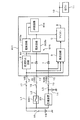
図5及び図6は第3実施形態の追加説明図を示している。図5に統合ECU301の別の構成例を示す。この統合ECU301は電源回路3に代えて電源回路303a、303bを複数設けている。統合ECU301のその他の構成は、統合ECU101と同様であるため説明を省略する。電源システムSY3は、逆流防止回路2、ダイオード6、7を備え、電源回路303a、303bを後段に接続して構成される。
Third Embodiment
5 and 6 show additional explanatory views of the third embodiment. Another structural example of integrated ECU301 is shown in FIG. The
この統合ECU301は、通常動作モードにおいて、電源回路303aが走行系/安全系機能を搭載した内部回路4、及び、マイコン9に電源供給すると共に、電源回路303bが一般機能を搭載した内部回路5に電源供給する。これらの電源回路303a、303bは互いに異なる直流電源電圧を出力する。このような場合、例えば、マイコン9が、内部回路5を省電力動作モードに移行させるときには、電源回路303bによる内部回路5への電流供給機能を通常動作モードに比較して低下させるようにしたり、電源回路303bによる内部回路5への電源供給経路を遮断するようにしても良い。
In the
また図6に統合ECU101に代わるECU401の別の構成例を示す。このECU401は、電源回路3に代えて電源回路303a、303bを複数設け、これらの複数の電源回路303a、303bが、例えば走行系/安全系機能又は一般機能を搭載した内部回路404に電源供給する。電源システムSY4は、逆流防止回路2、ダイオード6、7を備え、電源回路303a、303bを後段に接続して構成される。このような場合、例えばマイコン9が、内部回路404を省電力動作モードに移行させるときには、電源回路303bによる内部回路404への電流供給機能を通常動作モードに比較して低下させるようにしても良い。
Further, FIG. 6 shows another configuration example of the
(第4実施形態)
図7は第4実施形態の追加説明図を示している。前述実施形態で説明した機能は、多くの他の車両電源(例えば、アクセサリ電源ACC、イルミネーション電源ILL+)をサブ電源として用いた場合にも適用可能である。
Fourth Embodiment
FIG. 7 shows an additional explanatory view of the fourth embodiment. The functions described in the above embodiments are also applicable when many other vehicle power supplies (for example, accessory power supply ACC, illumination power supply ILL +) are used as sub power supplies.
例えば、図7に示すように、メイン電源供給ラインL1とサブ電源供給ラインL4との間にキースイッチSW2が接続されており、このキースイッチSW2がユーザ操作に応じてオンされることで、アクセサリ電源ACCがヒューズ29を通じて統合ECU101にサブ電源として入力端子27に入力される。キースイッチSW2は、キースイッチSW1が例えばACC又はONの位置でオンとなるスイッチであり、アクセサリ電源ACCはこのキースイッチSW2がオンされたときに出力される電源である。
For example, as shown in FIG. 7, a key switch SW2 is connected between the main power supply line L1 and the sub power supply line L4, and the key switch SW2 is turned on in response to a user operation. The power source ACC is input to the
また、メイン電源供給ラインL1とサブ電源供給ラインL5との間にキースイッチSW3が接続されており、このキースイッチSW3がユーザ操作に応じてオンされることで、イルミネーション電源ILL+がヒューズ30を通じて統合ECU101にサブ電源として入力端子28に入力される。イルミネーション電源ILL+は、車両内のスモールランプを点灯するときに出力される電源である。
Further, a key switch SW3 is connected between the main power supply line L1 and the sub power supply line L5, and the illumination power supply ILL + is integrated through the
入力端子27とノードN1との間にはダイオード31が順方向接続されている。また、入力端子28とノードN1との間にはダイオード32が順方向接続されている。電源システムSY5は、逆流防止回路2、ダイオード6、7、31、32を備え、電源回路3を後段に接続して構成されている。検出回路8は入力端子27、28の電圧を検出する。これにより、アクセサリ電源ACC、イルミネーション電源ILL+をサブ電源として適用した場合においても、前述実施形態と同様に適用できる。
The
(第5実施形態)
図8及び図9は第5実施形態の追加説明図を示している。第1、第2実施形態では、Nチャネル型のMOSFET21、22、221、222を用いて逆流防止回路2、202を構成した形態を示しているが、図8又は図9に示すように、Pチャネル型のMOSFET621、622、721、722を用いて逆流防止回路602、702を構成しても良い。
Fifth Embodiment
8 and 9 show an additional explanatory view of the fifth embodiment. In the first and second embodiments, the
例えば、図8に示す逆流防止回路602は、入力端子12と電源回路3の入力ノードN1との間に、MOSFET621のドレインD、ソースS、MOSFET622のソースS、ドレインD、検出抵抗24を直列接続して構成されている。これらのMOSFET621、622は、内部半導体構造上においてドレインDからソースSに向けて順方向の寄生ダイオード621a、622aが接続されている。逆流防止回路602がバッテリ電圧VBを入力電圧Vinとして入力すると、前述実施形態に説明したように、この入力電圧Vinよりも低い電圧がMOSFET621、622の共通ソースS、MOSFET622のドレインDに印加される。
For example, the
オンオフ制御部23は、MOSFET621、622をオン制御するときには、想定される入力電圧Vinよりも予め低く定められたオン制御電圧Vcon(VGSが閾値Vth未満となるように例えば0V)をゲートGに印加する。すると、電流が入力端子12からノードN1に流れ込む。オンオフ制御部23は、MOSFET621、622をオフ制御するときには、想定される入力電圧Vinよりも予め高く、もしくは閾値以内の定められたオフ制御電圧Vcoffを(VGSが閾値Vth以上となるように)ゲートGに印加する。するとMOSFET621、622はオフする。これにより、ノードN1の電圧が入力端子12の電圧よりも高くなったとしても逆流を防止できる。
When the on / off
例えば、図9に示す逆流防止回路702は、入力端子12と電源回路3の入力ノードN1との間に、MOSFET721のソースS、ドレインD、MOSFET722のドレインD、ソースS、検出抵抗24を直列接続して構成されている。これらのMOSFET721、722は、内部半導体構造上においてドレインDからソースSに向けて順方向の寄生ダイオード721a、722aが接続されている。逆流防止回路702がバッテリ電圧VBを入力電圧Vinとして入力すると、前述実施形態に説明したように、この入力電圧Vinよりも低い電圧がMOSFET721、722の共通ドレインD、MOSFET722のソースSに印加される。
For example, the
オンオフ制御部23は、MOSFET721、722をオン制御するときには、想定される入力電圧Vinよりも予め低く定められたオン制御電圧Vcon(VGSが閾値Vth以下となるように、例えば0V)をゲートGに印加する。すると、電流が入力端子12からノードN1に流れ込む。オンオフ制御部23は、MOSFET721、722をオフ制御するときには、想定される入力電圧Vinよりも予め高く、もしくは閾値以内の定められたオフ制御電圧Vcoffを(VGSが閾値Vth以上となるように)ゲートGに印加する。するとMOSFET721、722はオフする。これにより、ノードN1の電圧が入力端子12の電圧よりも高くなったとしても逆流を防止できる。
When the on / off
Pチャネル型のMOSFET621、622、721、722を用いた場合でもNチャネル型のMOSFET21、22、221、222を用いた場合と同様の作用効果を奏する。
Even when P-
(適用例)
以下、前述実施形態の様々な適用例を説明する。
近年の省燃費化の傾向からアイドリングストップ技術を用いている車両も存在する。このようなアイドリングストップ技術を用いた車両においては、エンジン起動していないにも拘わらず、車室内では車室内空間を快適にするための各種機器(例えばテレビやラジオなど)が動作する。これらの機器は、バッテリ電圧VBを電力消費し続けるため比較的消費電力が高く、バッテリ電圧VBの低下が顕著となる場合もある。また車両エンジンを始動したときにはクランキングを生じることになるが、このようなときにはバッテリ電圧VBが大きく低下する。特に、車両がアイドリングストップ状態となっているときにクランキングしたときには、特にバッテリ電圧VBの低下が顕著に現れる。
(Example of application)
Hereinafter, various application examples of the above-described embodiment will be described.
There are vehicles using idling stop technology from the tendency of fuel consumption improvement in recent years. In a vehicle using such an idling stop technology, various devices (for example, a television, a radio, etc.) for making the vehicle interior space comfortable operate in the vehicle interior even though the engine is not started. Since these devices continue to consume the battery voltage VB, the power consumption is relatively high, and the drop of the battery voltage VB may be remarkable. In addition, when the vehicle engine is started, cranking occurs, but in such a case, the battery voltage VB is greatly reduced. In particular, when cranking is performed when the vehicle is in the idling stop state, a drop in battery voltage VB is particularly noticeable.
このような場合、例えば第1実施形態を適用すれば、たとえアイドリングストップ状態からクランキング時にバッテリ電圧VBが低電圧になり、マイコン9が例えば図3のステップS4でNOと判定したとしても、例えばステップS8にてYESと判定すれば省電力動作モードに移行できる。このため、車両の走行/安全に関わる走行系/安全系機能による内部回路4を動作させ続けながら、一般機能を搭載した内部回路5を一部又は全部停止して省電力動作させることができる。これによりクランキング等のバッテリ電圧低下要因に基づくシステムのリセットを防ぐことができる。
In such a case, for example, if the first embodiment is applied, even if the battery voltage VB becomes low during cranking from the idling stop state, and the
またエンジン始動前には、バッテリ電源+Bが逆流防止回路2を通じて供給されている。このとき、マイコン9は車両ネットワークを通じてドア開閉情報を取得することでドア開状態を検出すると運転手が乗車すると判断できる。このドア開状態を検出したとき、マイコン9はスリープ状態から先行して通常動作モードに起動するようにしても良い。マイコン9が、先行して通常動作モードに起動されていれば、運転者がエンジン始動することでクランキングを生じたときに大電力を消費しバッテリ電圧VBが低下したとしても、ステップS4、S5、S8の電圧条件に応じて通常動作モード/省電力動作モードに切替えることで、全体システムのリセット、さらには再起動を防ぐことができる。これにより見かけ上の起動時間の短縮を図ることができる。
Also, before the engine is started, battery power + B is supplied through the
また従来、クランキング時にはマイコン9の内部データ抹消の防止のため、データの緊急退避制御(例えば不揮発性メモリへのデータ書込)の処理を行う場合もあったが、低電圧でも動作可能な省電力動作モードにおいては、このデータの緊急退避制御処理も行う必要がなくなる。
In the past, during cranking, there was also a case where emergency evacuation control of data (for example, data writing to a non-volatile memory) was performed to prevent internal data deletion of the
(他の実施形態)
本発明は前述した実施形態に限定されるものではなく、例えば、以下に示す変形又は拡張が可能である。
(Other embodiments)
The present invention is not limited to the embodiments described above, and, for example, the following modifications or expansions are possible.
例えば車両に適用するときには、必要に応じてイグニッション電源IGを搭載すれば良い。キースイッチSW1〜SW3は、回動操作式のものに限らずボタン式であっても良い。また、車両に拘わらず、メイン電源、サブ電源として機能する電源を備える様々な機器に有効である。 For example, when applied to a vehicle, the ignition power supply IG may be mounted as needed. The key switches SW1 to SW3 are not limited to the rotary operation type but may be a button type. Further, regardless of the vehicle, the present invention is effective for various devices provided with a power supply functioning as a main power supply and a sub power supply.
逆流防止回路2、102として、2つのMOSFET21、22又は221、222を用いた構成を示したが、1つ又は3つ以上のMOSFETを用いて逆流防止回路を構成しても良い。
Although two
例えば、一つの構成要素が有する機能を複数の構成要素に分散させたり、複数の構成要素が有する機能を一つの構成要素に統合させたりしてもよい。また前述の実施形態の構成の少なくとも一部を、同様の機能を有する公知の構成に置き換えてもよい。また、前述の2以上の実施形態の構成の一部又は全部を互いに組み合わせて付加しても置換しても良い。 For example, the functions of one component may be distributed to a plurality of components, or the functions of a plurality of components may be integrated into a single component. Further, at least a part of the configuration of the above-described embodiment may be replaced with a known configuration having the same function. In addition, some or all of the configurations of the two or more embodiments described above may be added or replaced in combination with each other.
特許請求の範囲に記載した括弧内の符号は、本発明の一つの態様として前述する実施形態に記載の具体的手段との対応関係を示すものであって、本発明の技術的範囲を限定するものではない。 The reference numerals in parentheses described in the claims indicate the correspondence with the specific means described in the embodiment described above as one aspect of the present invention, and limit the technical scope of the present invention It is not a thing.
図面中、4、5、404は内部回路(動作回路)、6、7、31、32はダイオード、9はマイコン(動作回路、制御部)、21、22、221、222はNチャネル型のMOSFET(MOSFET)、621、622、721、722はPチャネル型のMOSFET(MOSFET)、21a、22a、221a、222a、621a、622a、721a、722aは寄生ダイオード、23はオンオフ制御部、L1はメイン電源供給ライン、L2、L3はサブ電源供給ライン、+Bはバッテリ電源(メイン電源)、IGはイグニッション電源(サブ電源)、SUBは充電電源(サブ電源)、ACCはアクセサリ電源(サブ電源)、ILL+はイルミネーション電源(サブ電源)、N1はノード(共通接続ノード)、SY1、SY3、SY4、SY5は電源システム、を示す。
In the drawings, 4, 5, and 404 are internal circuits (operation circuits), 6, 7, 31, and 32 are diodes, 9 is a microcomputer (operation circuits and control unit), 21, 22, 221, and 222 are N-channel MOSFETs. (MOSFETs) 621 622 721 722 are P-
Claims (3)
前記サブ電源は、前記メイン電源からキースイッチ(SW1,SW2,SW3)のオンオフ操作により供給される電源、又は、前記メイン電源から充電装置(20)を通じて供給される電源であり、
MOSFET(21、22;221、222;621、622;721、722)、及び、前記メイン電源供給ラインから前記MOSFETを通じて電源供給される電源供給ノードの電圧(Vin、Vsense、Vout)に応じて前記MOSFETのゲートにオン制御電圧又はオフ制御電圧を印加するオンオフ制御部(23)を備え、前記オンオフ制御部が前記MOSFETのゲートにオン制御電圧を印加したときには前記メイン電源供給ラインから入力されるメイン電源を前記MOSFETを通じて前記共通接続ノードに出力し、前記オンオフ制御部が前記MOSFETのゲートにオフ制御電圧を印加したときには前記メイン電源供給ラインと前記共通接続ノードとの間の電気的接続を遮断することで逆流防止する逆流防止回路(2;102)と、
前記サブ電源供給ラインから前記共通接続ノードに向けて順方向電流が流れその逆流を防止するように接続されるダイオード(6、7;6、7、31、32)と、を備え、
前記オンオフ制御部が前記MOSFETのゲートにオン制御電圧を印加したときの前記メイン電源供給ラインから前記共通接続ノードへの前記メイン電源の降下電圧は、前記サブ電源供給ラインから前記共通接続ノードへの前記ダイオードによる前記サブ電源の降下電圧よりも低く設定されている電源システム。
The main power supply (+ B) input from the main power supply line (L1) and the sub power supplies (IG, SUB; IG, SUB, ACC, ILL +) input from the sub power supply lines (L2, L3; L2 to L5) Power supply system (SY1, SY3, SY4, SY5) which supplies) through one common connection node (N1),
The sub power source is a power source supplied from the main power source by on / off operation of a key switch (SW1, SW2, SW3), or a power source supplied from the main power source through a charging device (20).
MOSFETs (21, 22; 221, 222; 621, 622; 721, 722) and the voltages (Vin, Vsense, Vout) of the power supply nodes supplied with power from the main power supply line through the MOSFETs. An on / off control unit (23) for applying an on control voltage or an off control voltage to the gate of the MOSFET, the main being supplied from the main power supply line when the on / off control unit applies the on control voltage to the gate of the MOSFET A power supply is output to the common connection node through the MOSFET, and the on / off control unit cuts off an electrical connection between the main power supply line and the common connection node when an off control voltage is applied to the gate of the MOSFET. Backflow prevention circuit (2; 102) to prevent backflow by
And a diode (6, 7; 6, 7, 31, 32) connected so as to allow a forward current to flow from the sub power supply line to the common connection node so as to prevent the backflow thereof.
The voltage drop of the main power supply from the main power supply line to the common connection node when the on / off control unit applies an on control voltage to the gate of the MOSFET is from the sub power supply line to the common connection node. A power supply system set lower than a voltage drop of the sub power supply due to the diode.
前記MOSFETは、ドレイン同士又はソース同士が接続されると共に互いに逆極性で直列接続されると共にソースからドレイン又はドレインからソースに向けて順方向に寄生ダイオード(21a、22a;221a、222a;621a、622a;721a、722a)をそれぞれ備える少なくとも2つのMOSFET(21、22;221、222;621、622;721、722)により構成され、
前記オンオフ制御部は、前記メイン電源供給ラインから前記2つのMOSFETを通じて電源供給される複数の電源供給ノードのうち少なくとも2つの電源供給ノードの電圧の値に応じて前記2つのMOSFETのゲートにオン制御電圧又はオフ制御電圧を印加するものであり、
前記オンオフ制御部が前記2つのMOSFETのゲートにオン制御電圧を印加したときには前記メイン電源供給ラインに入力されるメイン電源を前記2つのMOSFETを通じて前記共通接続ノードに出力し、前記オンオフ制御部が前記2つのMOSFETのゲートにオフ制御電圧を印加したときには前記メイン電源供給ラインと前記共通接続ノードとの間の電気的接続を遮断することで逆流防止する電源システム。 In the power supply system according to claim 1,
The MOSFETs are connected in series between drains or sources and connected in reverse polarity with each other, and are parasitic diodes (21a, 22a; 221a, 222a; 621a, 622a in the forward direction from source to drain or drain to source) 721a, 722a), each comprising at least two MOSFETs (21, 22; 221, 222; 621, 622; 721, 722);
The on / off control unit controls on of the gates of the two MOSFETs according to the value of the voltage of at least two power supply nodes among the plurality of power supply nodes supplied with power from the main power supply line through the two MOSFETs. Apply a voltage or an off control voltage,
When the on / off control unit applies an on control voltage to the gates of the two MOSFETs, the main power supplied to the main power supply line is output to the common connection node through the two MOSFETs, and the on / off control unit A power supply system which prevents reverse current by interrupting an electrical connection between the main power supply line and the common connection node when an off control voltage is applied to the gates of two MOSFETs.
前記逆流防止回路及び前記ダイオードから前記共通接続ノードを通じて電源供給されることにより動作する動作回路(4、5、9、404)の動作モードを制御する制御部(9)を備え、
前記制御部は、前記メイン電源が予め定められたしきい値電圧以上であるときには前記動作回路を通常動作させる通常動作モードとし、前記メイン電源が前記しきい値電圧未満となるときには前記動作回路を前記通常動作よりも低消費電力となる省電力動作させる省電力動作モードとするように制御する電源システム。 In the power supply system according to claim 1 or 2,
The control circuit (9) controls an operation mode of an operation circuit (4, 5, 9, 404) which operates by being supplied with power from the diode through the common connection node and the backflow prevention circuit;
The control unit sets a normal operation mode in which the operation circuit operates normally when the main power supply is equal to or higher than a predetermined threshold voltage, and the control circuit operates the operation circuit when the main power supply is less than the threshold voltage. A power supply system that performs control so as to be a power saving operation mode for power saving operation that consumes less power than the normal operation.
Priority Applications (4)
| Application Number | Priority Date | Filing Date | Title |
|---|---|---|---|
| JP2016071660A JP6531695B2 (en) | 2016-03-31 | 2016-03-31 | Power supply system |
| PCT/JP2017/007135 WO2017169395A1 (en) | 2016-03-31 | 2017-02-24 | Power supply system |
| DE112017001674.6T DE112017001674B4 (en) | 2016-03-31 | 2017-02-24 | power supply system |
| US16/088,923 US10862324B2 (en) | 2016-03-31 | 2017-02-24 | Power supply system |
Applications Claiming Priority (1)
| Application Number | Priority Date | Filing Date | Title |
|---|---|---|---|
| JP2016071660A JP6531695B2 (en) | 2016-03-31 | 2016-03-31 | Power supply system |
Publications (3)
| Publication Number | Publication Date |
|---|---|
| JP2017184538A JP2017184538A (en) | 2017-10-05 |
| JP2017184538A5 JP2017184538A5 (en) | 2018-03-15 |
| JP6531695B2 true JP6531695B2 (en) | 2019-06-19 |
Family
ID=59964108
Family Applications (1)
| Application Number | Title | Priority Date | Filing Date |
|---|---|---|---|
| JP2016071660A Active JP6531695B2 (en) | 2016-03-31 | 2016-03-31 | Power supply system |
Country Status (4)
| Country | Link |
|---|---|
| US (1) | US10862324B2 (en) |
| JP (1) | JP6531695B2 (en) |
| DE (1) | DE112017001674B4 (en) |
| WO (1) | WO2017169395A1 (en) |
Families Citing this family (11)
| Publication number | Priority date | Publication date | Assignee | Title |
|---|---|---|---|---|
| JP6626741B2 (en) * | 2016-03-01 | 2019-12-25 | 矢崎総業株式会社 | Battery system controller |
| JP6531695B2 (en) | 2016-03-31 | 2019-06-19 | 株式会社デンソー | Power supply system |
| DE102017201893A1 (en) * | 2017-01-12 | 2018-07-12 | Continental Teves Ag & Co. Ohg | Electronic circuit for securing a power supply of a receiving device |
| US10752116B2 (en) * | 2018-03-16 | 2020-08-25 | Ford Global Technologies, Llc | Vehicle backup electrical power system |
| CN109649309B (en) * | 2019-01-31 | 2020-09-04 | 宁德时代新能源科技股份有限公司 | Control system |
| US11539201B2 (en) * | 2019-03-04 | 2022-12-27 | Portwell Inc. | Reverse polarity protection device |
| JP7294127B2 (en) | 2019-12-26 | 2023-06-20 | 株式会社オートネットワーク技術研究所 | Power supply controller |
| US11296490B2 (en) * | 2020-04-07 | 2022-04-05 | Hitachi Astemo Americas, Inc. | Ground fault control for multiple ground paths |
| EP3971041A1 (en) | 2020-09-21 | 2022-03-23 | Veoneer Sweden AB | Ecu with power supply management and method for power supply of an ecu |
| US11563324B2 (en) * | 2020-09-30 | 2023-01-24 | Pony Ai Inc. | Power distribution system with redundancy to increase safety factor |
| DE102022116806A1 (en) | 2022-07-06 | 2024-01-11 | AT Tronic GmbH | Method and circuit for current control |
Family Cites Families (10)
| Publication number | Priority date | Publication date | Assignee | Title |
|---|---|---|---|---|
| JPS592532A (en) * | 1982-06-28 | 1984-01-09 | 日本電気株式会社 | Parallel operating device for power sources |
| JPH07194027A (en) * | 1993-12-27 | 1995-07-28 | Hitachi Ltd | Uninterruptible power supply apparatus |
| JP4053447B2 (en) | 2003-03-13 | 2008-02-27 | 株式会社オートネットワーク技術研究所 | Vehicle power supply circuit |
| JP2009183020A (en) * | 2008-01-29 | 2009-08-13 | Panasonic Corp | Power supply circuit device of mobile apparatus |
| JP2010098827A (en) * | 2008-10-15 | 2010-04-30 | Nippon Telegr & Teleph Corp <Ntt> | Charge/discharge control method, charge/discharge controller, and self-supporting power supply system |
| JP5376641B2 (en) * | 2009-02-27 | 2013-12-25 | Necエナジーデバイス株式会社 | Battery device |
| JP2011166918A (en) * | 2010-02-08 | 2011-08-25 | Sanyo Electric Co Ltd | Power supply system |
| WO2015145733A1 (en) * | 2014-03-28 | 2015-10-01 | 三菱電機株式会社 | Vehicle-mounted device |
| JP6355505B2 (en) | 2014-09-30 | 2018-07-11 | Kddi株式会社 | Settlement management device and settlement management method |
| JP6531695B2 (en) | 2016-03-31 | 2019-06-19 | 株式会社デンソー | Power supply system |
-
2016
- 2016-03-31 JP JP2016071660A patent/JP6531695B2/en active Active
-
2017
- 2017-02-24 WO PCT/JP2017/007135 patent/WO2017169395A1/en active Application Filing
- 2017-02-24 DE DE112017001674.6T patent/DE112017001674B4/en not_active Expired - Fee Related
- 2017-02-24 US US16/088,923 patent/US10862324B2/en active Active
Also Published As
| Publication number | Publication date |
|---|---|
| DE112017001674B4 (en) | 2022-06-02 |
| JP2017184538A (en) | 2017-10-05 |
| WO2017169395A1 (en) | 2017-10-05 |
| US10862324B2 (en) | 2020-12-08 |
| US20190109479A1 (en) | 2019-04-11 |
| DE112017001674T5 (en) | 2018-12-13 |
Similar Documents
| Publication | Publication Date | Title |
|---|---|---|
| JP6531695B2 (en) | Power supply system | |
| JP4479797B2 (en) | Electronic control unit | |
| JP5360245B2 (en) | Power storage device | |
| US9030041B2 (en) | On-vehicle electronic control apparatus | |
| WO2018047636A1 (en) | On-vehicle backup device | |
| JP2007082374A (en) | Protection circuit on reverse connection of power supply | |
| JP2002315182A (en) | Active circuit protection for switch type power supply system | |
| JP2007312543A (en) | Power supply module | |
| JP7113228B2 (en) | Vehicle power storage device | |
| JP6408843B2 (en) | Vehicle power supply device | |
| CN111630763B (en) | Boost type switching power supply circuit | |
| JP2017001539A (en) | Airbag control device and semiconductor device | |
| JP6112004B2 (en) | Auxiliary power supply | |
| JP6493874B2 (en) | Switch monitoring circuit | |
| US20130002019A1 (en) | Circuit, Method for Operating a Circuit, and Use | |
| JP2013247823A (en) | Semiconductor device | |
| JP6031672B2 (en) | In-vehicle power supply device and in-vehicle power supply unit using the same | |
| WO2020008732A1 (en) | Boosting power supply circuit | |
| JP2004159410A (en) | Power supply device and power control method | |
| US20220416318A1 (en) | In-Vehicle Power Source Control Apparatus and In-Vehicle Power Source Apparatus | |
| JPH11338556A (en) | Power circuit | |
| WO2023228287A1 (en) | Power feed control device | |
| WO2024024087A1 (en) | On-vehicle backup control device | |
| US10734827B2 (en) | Power supply system | |
| WO2014104332A1 (en) | Power supply device |
Legal Events
| Date | Code | Title | Description |
|---|---|---|---|
| A521 | Request for written amendment filed |
Free format text: JAPANESE INTERMEDIATE CODE: A523 Effective date: 20180201 |
|
| A621 | Written request for application examination |
Free format text: JAPANESE INTERMEDIATE CODE: A621 Effective date: 20180201 |
|
| TRDD | Decision of grant or rejection written | ||
| A01 | Written decision to grant a patent or to grant a registration (utility model) |
Free format text: JAPANESE INTERMEDIATE CODE: A01 Effective date: 20190423 |
|
| A61 | First payment of annual fees (during grant procedure) |
Free format text: JAPANESE INTERMEDIATE CODE: A61 Effective date: 20190506 |
|
| R151 | Written notification of patent or utility model registration |
Ref document number: 6531695 Country of ref document: JP Free format text: JAPANESE INTERMEDIATE CODE: R151 |
|
| R250 | Receipt of annual fees |
Free format text: JAPANESE INTERMEDIATE CODE: R250 |
|
| R250 | Receipt of annual fees |
Free format text: JAPANESE INTERMEDIATE CODE: R250 |