JP6524000B2 - Power converter - Google Patents
Power converter Download PDFInfo
- Publication number
- JP6524000B2 JP6524000B2 JP2016050527A JP2016050527A JP6524000B2 JP 6524000 B2 JP6524000 B2 JP 6524000B2 JP 2016050527 A JP2016050527 A JP 2016050527A JP 2016050527 A JP2016050527 A JP 2016050527A JP 6524000 B2 JP6524000 B2 JP 6524000B2
- Authority
- JP
- Japan
- Prior art keywords
- switch
- phase
- voltage
- arm
- control unit
- Prior art date
- Legal status (The legal status is an assumption and is not a legal conclusion. Google has not performed a legal analysis and makes no representation as to the accuracy of the status listed.)
- Active
Links
Images


Classifications
-
- H—ELECTRICITY
- H02—GENERATION; CONVERSION OR DISTRIBUTION OF ELECTRIC POWER
- H02M—APPARATUS FOR CONVERSION BETWEEN AC AND AC, BETWEEN AC AND DC, OR BETWEEN DC AND DC, AND FOR USE WITH MAINS OR SIMILAR POWER SUPPLY SYSTEMS; CONVERSION OF DC OR AC INPUT POWER INTO SURGE OUTPUT POWER; CONTROL OR REGULATION THEREOF
- H02M7/00—Conversion of ac power input into dc power output; Conversion of dc power input into ac power output
- H02M7/42—Conversion of dc power input into ac power output without possibility of reversal
- H02M7/44—Conversion of dc power input into ac power output without possibility of reversal by static converters
- H02M7/48—Conversion of dc power input into ac power output without possibility of reversal by static converters using discharge tubes with control electrode or semiconductor devices with control electrode
- H02M7/483—Converters with outputs that each can have more than two voltages levels
- H02M7/487—Neutral point clamped inverters
-
- H—ELECTRICITY
- H02—GENERATION; CONVERSION OR DISTRIBUTION OF ELECTRIC POWER
- H02M—APPARATUS FOR CONVERSION BETWEEN AC AND AC, BETWEEN AC AND DC, OR BETWEEN DC AND DC, AND FOR USE WITH MAINS OR SIMILAR POWER SUPPLY SYSTEMS; CONVERSION OF DC OR AC INPUT POWER INTO SURGE OUTPUT POWER; CONTROL OR REGULATION THEREOF
- H02M7/00—Conversion of ac power input into dc power output; Conversion of dc power input into ac power output
- H02M7/42—Conversion of dc power input into ac power output without possibility of reversal
- H02M7/44—Conversion of dc power input into ac power output without possibility of reversal by static converters
- H02M7/48—Conversion of dc power input into ac power output without possibility of reversal by static converters using discharge tubes with control electrode or semiconductor devices with control electrode
- H02M7/483—Converters with outputs that each can have more than two voltages levels
- H02M7/49—Combination of the output voltage waveforms of a plurality of converters
-
- H—ELECTRICITY
- H02—GENERATION; CONVERSION OR DISTRIBUTION OF ELECTRIC POWER
- H02M—APPARATUS FOR CONVERSION BETWEEN AC AND AC, BETWEEN AC AND DC, OR BETWEEN DC AND DC, AND FOR USE WITH MAINS OR SIMILAR POWER SUPPLY SYSTEMS; CONVERSION OF DC OR AC INPUT POWER INTO SURGE OUTPUT POWER; CONTROL OR REGULATION THEREOF
- H02M7/00—Conversion of ac power input into dc power output; Conversion of dc power input into ac power output
- H02M7/42—Conversion of dc power input into ac power output without possibility of reversal
- H02M7/44—Conversion of dc power input into ac power output without possibility of reversal by static converters
- H02M7/48—Conversion of dc power input into ac power output without possibility of reversal by static converters using discharge tubes with control electrode or semiconductor devices with control electrode
- H02M7/483—Converters with outputs that each can have more than two voltages levels
- H02M7/4835—Converters with outputs that each can have more than two voltages levels comprising two or more cells, each including a switchable capacitor, the capacitors having a nominal charge voltage which corresponds to a given fraction of the input voltage, and the capacitors being selectively connected in series to determine the instantaneous output voltage
-
- H—ELECTRICITY
- H02—GENERATION; CONVERSION OR DISTRIBUTION OF ELECTRIC POWER
- H02M—APPARATUS FOR CONVERSION BETWEEN AC AND AC, BETWEEN AC AND DC, OR BETWEEN DC AND DC, AND FOR USE WITH MAINS OR SIMILAR POWER SUPPLY SYSTEMS; CONVERSION OF DC OR AC INPUT POWER INTO SURGE OUTPUT POWER; CONTROL OR REGULATION THEREOF
- H02M1/00—Details of apparatus for conversion
- H02M1/0003—Details of control, feedback or regulation circuits
-
- H—ELECTRICITY
- H02—GENERATION; CONVERSION OR DISTRIBUTION OF ELECTRIC POWER
- H02M—APPARATUS FOR CONVERSION BETWEEN AC AND AC, BETWEEN AC AND DC, OR BETWEEN DC AND DC, AND FOR USE WITH MAINS OR SIMILAR POWER SUPPLY SYSTEMS; CONVERSION OF DC OR AC INPUT POWER INTO SURGE OUTPUT POWER; CONTROL OR REGULATION THEREOF
- H02M1/00—Details of apparatus for conversion
- H02M1/0064—Magnetic structures combining different functions, e.g. storage, filtering or transformation
-
- H—ELECTRICITY
- H02—GENERATION; CONVERSION OR DISTRIBUTION OF ELECTRIC POWER
- H02M—APPARATUS FOR CONVERSION BETWEEN AC AND AC, BETWEEN AC AND DC, OR BETWEEN DC AND DC, AND FOR USE WITH MAINS OR SIMILAR POWER SUPPLY SYSTEMS; CONVERSION OF DC OR AC INPUT POWER INTO SURGE OUTPUT POWER; CONTROL OR REGULATION THEREOF
- H02M1/00—Details of apparatus for conversion
- H02M1/0095—Hybrid converter topologies, e.g. NPC mixed with flying capacitor, thyristor converter mixed with MMC or charge pump mixed with buck
Landscapes
- Engineering & Computer Science (AREA)
- Power Engineering (AREA)
- Inverter Devices (AREA)
Description
本発明の実施形態は、直流電源と交流電力系統との間に設置され、交流と直流を相互に変換する電力変換装置に関する。 The embodiment of the present invention relates to a power conversion device which is installed between a DC power supply and an AC power system, and converts AC and DC mutually.
近年、風力発電や太陽光発電、太陽熱発電などの再生可能エネルギーの普及が促進されている。より大電力を再生可能エネルギーでまかなうために、洋上風力発電や、砂漠地帯での太陽光や太陽熱発電が検討されている。洋上風力発電等においては、発電電力を洋上から消費地である都市まで海底ケーブルで大電力送電したり、アフリカや中国奥部の砂漠地帯から、ヨーロッパや沿岸地帯の大都市まで大電力を長距離にわたって高効率に送電したりすることが必要になる。このような要求には、従来の三相交流による電力送電よりも直流送電のほうが高効率であり、コストを抑えながら設置することが可能になるため、直流送電網の構築が検討され始めている。 In recent years, the spread of renewable energy such as wind power generation, solar power generation and solar thermal power generation has been promoted. In order to provide more electricity with renewable energy, offshore wind power generation and solar and solar power generation in desert areas are being considered. In offshore wind power generation, large-power transmission of generated power from the ocean to a city where it is consumed by submarine cables or long distances from large desert areas in Africa and China to large cities in Europe and coastal areas It is necessary to transmit electricity with high efficiency. In order to meet such requirements, DC transmission is more efficient than conventional three-phase AC power transmission, and it becomes possible to install while suppressing the cost, so construction of a DC transmission network is being studied.
直流送電においては、発電された交流電力を直流送電用の直流に変換するコンバータや、送電されてきた直流を都市内の交流に変換するインバータなどの電力変換装置が必要になる。現在、交流系統にコンバータ、インバータのスイッチングに伴う高調波が流出しないように、正弦波に近い電圧波形を出力することができ、出力フィルタを削減できる電力変換装置が実用化されている。この電力変換装置は、MMC(Modular Multilevel Converter)と呼ばれる。 In DC power transmission, a power converter such as a converter for converting generated AC power to DC for DC power transmission or an inverter for converting DC power transmitted to AC in a city is required. At present, a power converter capable of outputting a voltage waveform close to a sine wave and reducing an output filter has been put to practical use so that harmonics accompanying switching of a converter and an inverter do not flow out to the AC system. This power converter is called an MMC (Modular Multilevel Converter).
MMCは、直流電源と交流電力系統との間に設けられる。三相交流に変換する場合、MMCは三相の相アームを有する。三相の相アームは、チョッパセルを直列接続して成る。三相の相アームは並列接続され、直流電源と各々が常時接続されている。各相アームは上アームと下アームに分別される。すなわち、MMCにおいて、直列接続されたチョッパセル群は2つの群に分けられ、各チョッパセル郡は上アームと下アームと呼ばれ、上アームと下アームの間には交流電力系統への出力端子が設けられている。上アームと出力端子との間、及び下アームと出力端子との間には、各々リアクトルが挿入され、上アームと下アームとの短絡による電流増大を抑制している。 The MMC is provided between the DC power supply and the AC power system. When converting to a three-phase alternating current, the MMC has a three-phase phase arm. Three-phase phase arms are formed by connecting chopper cells in series. The three phase arms are connected in parallel, and are always connected to DC power supplies. Each phase arm is divided into an upper arm and a lower arm. That is, in MMC, chopper cell groups connected in series are divided into two groups, each chopper cell group is called an upper arm and a lower arm, and an output terminal to an AC power system is provided between the upper arm and the lower arm. It is done. A reactor is inserted between the upper arm and the output terminal and between the lower arm and the output terminal, respectively, to suppress an increase in current due to a short circuit between the upper arm and the lower arm.
MMCは、チョッパセルのコンデンサに出力交流周波数と同等の電力脈動が原理的に生じる。コンデンサ電圧の変動を一定の値以下に抑制するには、コンデンサの容量を大きくする必要がある。直流電圧が数十kV〜数百kVに及ぶ直流送電の場合、チョッパセルの数が多く、それに比例してコンデンサ体積が大きくなってしまう。 In principle, MMC generates power pulsation equivalent to the output AC frequency in the capacitor of the chopper cell. In order to suppress the fluctuation of the capacitor voltage to a predetermined value or less, it is necessary to increase the capacity of the capacitor. In the case of direct current transmission where the direct current voltage is in the range of tens of kV to hundreds of kV, the number of chopper cells is large, and in proportion to that, the capacitor volume is increased.
そこで、近年、IGBT等の自励式のスイッチを多直列接続したバルブと、チョッパセルを組み合わせた中性点クランプ形モジュラー・マルチレベル・コンバータ(NPC−MMC)が提案されている。NPC−MMCは、三相の相アームの両端に第1スイッチ及び第4スイッチを備え、三相の相アームを第1スイッチ及び第4スイッチを介して直流電源と各々接続させている。また、NPC−MMCは、第1スイッチと第4スイッチの間に直列接続された第2スイッチと第3スイッチを更に備え、この第2スイッチと第3スイッチを相アームと並列に接続させている。 Therefore, in recent years, a neutral point clamp modular multilevel converter (NPC-MMC) has been proposed in which a valve in which multiple self-excited switches such as IGBTs are connected in series and a chopper cell are combined. The NPC-MMC has a first switch and a fourth switch at both ends of a three-phase phase arm, and connects the three-phase phase arm to a DC power supply via the first switch and the fourth switch, respectively. In addition, the NPC-MMC further includes a second switch and a third switch connected in series between the first switch and the fourth switch, and the second switch and the third switch are connected in parallel with the phase arm. .
NPC−MMCは、各スイッチのオンオフ操作によって、一相を他の二相と直列接続し、他の二相を並列接続し、この接続関係を有する三相のアームを直流電源と接続する。そのため、NPC−MMCは、各相のチョッパセルの数を半分にでき、装置の設置スペースが低減し、スイッチング損失が低減して変換効率が向上する。 The NPC-MMC connects one phase in series with the other two phases, connects the other two phases in parallel, and connects a three-phase arm having this connection relationship with a DC power supply by the on / off operation of each switch. Therefore, in the NPC-MMC, the number of chopper cells of each phase can be halved, the installation space of the apparatus is reduced, the switching loss is reduced, and the conversion efficiency is improved.
NPC−MMCは、第2スイッチと第3スイッチの間に中性点を備える。一般的には、直列接続された入力直流コンデンサの対が相アームに対して並列接続され、また第2スイッチと第3スイッチの間と入力直流コンデンサの間とが結線されることで、第2スイッチと第3スイッチとの間に中性点が生成される。但し、入力直流コンデンサの存在が、NPC−MMCの有する小型化という利点を希薄にしている。そこで、近年は、中性点同士を接続することで、入力直流コンデンサを省略したNPC−MMCも提案されている。 The NPC-MMC has a neutral point between the second switch and the third switch. Generally, the pair of series-connected input DC capacitors are connected in parallel to the phase arm, and the second switch is connected to the third switch and the input DC capacitor is connected. A neutral point is generated between the switch and the third switch. However, the presence of the input DC capacitor thins out the advantage of the NPC-MMC's miniaturization. Therefore, in recent years, an NPC-MMC in which an input DC capacitor is omitted by connecting neutral points has been proposed.
NPC−MMCは、直列接続された二相によって直流電源の正側と負側とを繋ぐため、各相の多直列接続された第1スイッチ乃至第4スイッチは直流入力電圧の半分以上の耐電圧を有していればよい。しかしながら、入力直流コンデンサを排除したNPC−MMCにおいては、三相の繋ぎ変え前にリアクトルを含む電流経路内に存在し、三相の繋ぎ変えによりオンからオフに転じるスイッチに、直流電源の直流入力電圧が印加されてしまうことがあった。そのため、スイッチは直流入力電圧以上の耐電圧が要求されることになる。 Since the NPC-MMC connects the positive side and the negative side of the DC power supply by two phases connected in series, the first to fourth switches connected in series with each phase have withstand voltages of half or more of the DC input voltage As long as you have However, in the NPC-MMC excluding the input DC capacitor, the DC input of the DC power supply is present in the current path including the reactor before the three-phase reconnection, and switches from on to off by the three-phase reconnection. The voltage may be applied. Therefore, the switch is required to have a withstand voltage higher than the DC input voltage.
例えば、図20の(a)に示すように、U相の第2スイッチ42及び第4スイッチ44とV相の第1スイッチ41及び第3スイッチ43がオンであり、その他がオフの状態がある。この状態では、U相の上アーム21とU相の出力端子23との間のリアクトル7、U相の上アーム21、U相の第2スイッチ42、U相の中性点5、V相の中性点5、V相の第3スイッチ43、V相の下アーム22、及びV相の下アーム22とV相の出力端子23との間のリアクトル7を経る循環交流電流Icの電流経路が発生する。
For example, as shown in (a) of FIG. 20, the U-phase
図20の(b)に示すように、三相の繋ぎ変えのために、例えばU相の第2スイッチ22が先行してオフになった場合、U相の上アーム21とU相の出力端子23との間のリアクトル7、及びV相の下アーム22とV相の出力端子23との間のリアクトル7が各々に流れる循環交流電流Icの維持を図るために、U相の上アーム21とU相の出力端子23との間のリアクトル7、U相の上アーム21、U相の第1スイッチ41、直流電源100、U相の第4スイッチ44、U相の第3スイッチ43、U相の中性点5、V相の中性点5、V相の第3スイッチ43、V相の下アーム22、及びV相の下アーム22とV相の出力端子23との間のリアクトル7という循環交流電流Icの電流経路が発生する。
As shown in (b) of FIG. 20, for example, when the U-phase
そうすると、図20の(b)に示すように、オフになったU相の第2スイッチ42には、直流電源100の直流入力電圧が印加されることになる。従って、第1乃至第4スイッチ41〜44には直流電源100の直流入力電圧以上の耐電圧が要求される。耐電圧を向上させるには、第1乃至第4スイッチ41〜44の構成要素であるスイッチング素子の数を増加させなければならない。スイッチング素子の増加は、NPC−MMCのコスト増及び大型化を招来する。
Then, as shown in (b) of FIG. 20, the DC input voltage of the
そこで、本発明の実施形態は、入力直流コンデンサを排除しつつ、多直列に接続されたスイッチの耐電圧を下げても支障のないNPC−MMCの電力変換装置を提供することを目的とする。 Therefore, an object of the embodiments of the present invention is to provide an NPC-MMC power converter that does not have any problem even if the withstand voltage of switches connected in multiple series is reduced while excluding input DC capacitors.
上記の目的を達成するために、本実施形態の電力変換装置は、直流電源と交流電力系統との間に設けられ、交流と直流を相互に変換する電力変換装置であって、複数のチョッパセルを直列接続して成る複数相の各相アームと、前記相アーム内の前記チョッパセルを2つに分けて成る上アーム及び下アームと、前記上アームと前記下アームとの間に設けられ、前記交流電力系統と接続される出力端子と、前記相アームの両端に設けられ、前記相アームと前記直流電源との間に介在する第1スイッチ及び第4スイッチと、前記第1スイッチと前記第4スイッチとの間に直列接続され、前記相アームと並列接続される第2スイッチ及び第3スイッチと、前記第2スイッチと前記第3スイッチとの間に設けられ、互いに結線される前記複数相の各中性点と、前記複数相の各中性点間に介在するリアクトルと、
を備えること、を特徴とする。
In order to achieve the above object, the power conversion device of the present embodiment is a power conversion device which is provided between a DC power supply and an AC power system and converts AC and DC mutually, and includes a plurality of chopper cells. A plurality of phase arms connected in series, an upper arm and a lower arm formed by dividing the chopper cell in the phase arm into two, an arm provided between the upper arm and the lower arm, and the AC An output terminal connected to the electric power system, and first and fourth switches provided at both ends of the phase arm and interposed between the phase arm and the DC power supply, the first switch, and the fourth switch Between the second switch and the third switch connected in series with each other and in parallel with the phase arm, and between the second switch and the third switch, the plurality of phases being mutually connected neutral When a reactor interposed between the neutral point of the plurality of phases,
Providing.
(構成)
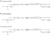
以下、本実施形態の電力変換装置について図面を参照しつつ詳細に説明する。図1は、本実施形態の電力変換装置の構成図である。図2は、電力変換装置が備えるチョッパセルの構成図である。電力変換装置1は、中性点クランプ形モジュラー・マルチレベル・コンバータ(NPC−MMC)であり、高圧直流送電システムに備えられる。電力変換装置1は、直流電源100と交流電力系統200との間に設置される。電力変換装置1は、直流電源100の入力直流電圧v_dcを三相の交流電圧v_acに変換し、三相トランス201を介して交流電力を交流電力系統200に出力する。
(Constitution)
Hereinafter, the power conversion device of the present embodiment will be described in detail with reference to the drawings. FIG. 1 is a block diagram of the power conversion device of this embodiment. FIG. 2: is a block diagram of the chopper cell with which a power converter device is provided. The
この電力変換装置1は、U相、V相及びW相の各交流電圧v_acを生成する相アーム2を備えている。各相アーム2は、両端が第1スイッチ41と第4スイッチ44と接続し、第1スイッチ41及び第4スイッチ44を介して直流電源100と接続される。この各相アーム2は複数のチョッパセル3を直列接続して成る。
The
チョッパセル3は、図2に示すように、スイッチ31とスイッチ32を直列接続したレグと、直流コンデンサ33とを並列接続してなる。スイッチ31及び32は逆導通スイッチであり、各スイッチ31及び32のスイッチング素子に各々帰還ダイオード33を逆並列に接続して構成される。スイッチング素子は、例えば、オン時には電流を一方向に流すIGBTやMOSFET等であり、自己消弧能力を有する。
As shown in FIG. 2, the
各相アーム2では、チョッパセル3が上アーム21と下アーム22に区別されている。上アーム21は、直流電源100から見て正側に接続されたチョッパセル3群である。下アーム22は、直流電源100から見て負側に接続されたチョッパセル3群である。相アーム2は、上アーム21と下アーム22との間に出力端子23を備え、出力端子23から三相トランス201を介して交流電力系統200へ交流電力v_acを出力する。
In each
各相アーム2は、チョッパセル3を単位変換器として直流電圧v_dcを階段状の交流電圧v_acに変換する。各相アーム2が有するチョッパセル3の数は、入力直流電圧v_dcと、チョッパセル3のコンデンサ電圧v_chによって決定され、概ね(v_dc/2)/v_chである。本実施形態では、チョッパセル3の数を3としている。
Each
また、電力変換装置1は、第1スイッチ41及び第4スイッチ44を構成要素とするバルブ4を各相に更に備える。バルブ4は、第1スイッチ41及び第4スイッチ44の他、第2スイッチ42及び第3スイッチ43を備える。これら第1乃至第4スイッチ41〜44を直列接続される。第2スイッチ42と第3スイッチ43は、第1スイッチ41と第4スイッチ44との間に直列接続され、相アーム2と並列接続されている。バルブ4は、第1乃至第4スイッチ41〜44のオンオフにより、60度の電圧位相角毎に各相アーム2の接続関係を切り替える。
In addition, the
第1乃至第4スイッチ41、42、43及び44は逆導通スイッチであり、スイッチング素子に帰還ダイオードを逆並列に接続して構成される。スイッチング素子は、例えば、オン時には電流を一方向に流すIGBTやMOSFET等であり、自己消弧能力を有する。
The first to
第1乃至第4スイッチ41、42、43及び44は、直流電源100の入力直流電圧v_dcにより耐電圧が決定される。入力直流電圧v_dcに対して、v_dc/2の電圧にスイッチング時のサージ電圧の重畳を考慮し、使用する素子が決定される。入力直流電圧v_dcが数十kV以上に及ぶと、1素子で耐電圧を持たせることは困難になり、複数の素子を直列にする必要がある。本実施形態では1つのスイッチに対し1素子を含むが、1つのスイッチに複数の素子が直列接続して含まれていてもよい。
The withstand voltage of each of the first to
第1スイッチ41及び第4スイッチ44の方向に関し、第1スイッチ41は、コレクタで直流電源100の正側と接続され、エミッタで上アーム21のコレクタと接続される。第4スイッチ44は、エミッタで直流電源100の負側と接続され、コレクタで下アーム22のエミッタと接続される。第2スイッチ42及び第3スイッチ43の方向に関し、第2スイッチ42のコレクタが、上アーム21と接続する第1スイッチ41のエミッタと接続され、第3スイッチ43のエミッタが、下アーム22と接続した第4スイッチ44のコレクタと接続されている。
With respect to the directions of the
U相の第2スイッチ42と第3スイッチ43の間には中性点5が設けられ、V相の第2スイッチ42と第3スイッチ43の間には中性点5が設けられ、W相の第2スイッチ42と第3スイッチ43の間には中性点5が設けられている。各中性点5は、各々がリアクトル7と接続しており、三相の各リアクトル7を介して互いに結線されている。
A
(制御)
このような電力変換装置1は、図3に示すように、60度の電圧位相ごとに、各種組み合わせで、一相と他二相とを直列接続し、他二相を並列接続し、また並列二相と単独一相を正側又は負側に入れ替える。
(control)
As shown in FIG. 3, such a
例えば、図3の(a)及び図4に示すように、U相の電圧位相がπ/3〜2π/3のとき、V相とW相の相アーム2を並列接続し、並列接続された相アーム2とU相の相アーム2を直列接続し、V相とW相の相アーム2を直流電源100の負側に接続し、U相の相アーム2を直流電源100の正側に接続する。
For example, as shown in FIG. 3A and FIG. 4, when the voltage phase of the U phase is π / 3 to 2π / 3, the
この接続態様の回路は、バルブ4において次のようなスイッチオンオフにより実現する。すなわち、U相の第1スイッチ41と第3スイッチ43をオンにし、V相の第2スイッチ42と第4スイッチ43をオンにし、W相の第2スイッチ42と第4スイッチ44をオンにする。
The circuit of this connection mode is realized by switching on and off the valve 4 as follows. That is, the U-phase
また、例えば、図3の(b)及び図4に示すように、U相の電圧位相が4π/3〜5π/3のとき、V相とW相の相アーム2を直流電源20の並列接続し、並列接続された相アーム2とU相の相アーム2を直列接続し、V相とW相の相アーム2を直流電源100の正側に接続し、U相の相アーム2を直流電源100の負側に接続する。
Further, for example, as shown in (b) of FIG. 3 and FIG. 4, when the voltage phase of the U phase is 4π / 3 to 5π / 3, the
この接続態様の回路は、バルブ4において次のようなスイッチオンオフにより実現する。すなわち、バルブ4は、V相の第1スイッチ41と第3スイッチ43をオンにし、W相の第1スイッチ41と第3スイッチ43をオンにし、U相の第2スイッチ42と第4スイッチ44をオンにする。
The circuit of this connection mode is realized by switching on and off the valve 4 as follows. That is, the valve 4 turns on the V phase
電力変換装置1を動作させると、例えば、U相の出力交流電圧v_ac_uが正でV相の出力交流電圧v_ac_vが負のとき、U相の相アーム2のコンデンサ電圧v_up+v_unとV相の相アーム2のコンデンサ電圧v_vp+v_vnとを合計した電圧が、U相の第1スイッチ41、第3スイッチ43、V相の第2スイッチ42及び第4スイッチ44を通して、入力直流電圧v_dcと短絡される。リアクトル7は、この短絡の際の電流増大を抑制している。
When
この電力変換装置1では、図3に示すように、直流電源100と電力変換装置1との間に、PN間循環電流が流れる。PN間循環電流は、電力変換装置1に形成された回路を直流電源100の正側から負側へ抜ける電流である。また、並列接続された二相の相アーム2間に、相間循環電流が流れる。相間循環直流電流は、並列接続された二相の相アーム2を循環する電流である。
In the
(電圧制御)
この電力変換装置1の制御方法について説明する。図5に示すように、電力変換装置1は制御部6を備える。制御部6は、各相アーム2のチョッパセル3と各相の第1乃至第4スイッチ41、42、43及び44を制御する。制御部6は、プログラムに従って演算及び制御する所謂コンピュータ又は専用の電気回路である。例えば、制御部6では、ROMに記憶されたプログラムに従ってCPUが演算し、演算結果に従って各相アーム2のチョッパセル3と各相の第1乃至第4スイッチ41、42、43及び44に対する駆動回路がゲート信号を送信する。この制御部6には、不図示の電流検出器及び電圧検出器によって各上アーム21及び下アーム22で検出された電流及び電圧の値が入力され、電流値及び電圧値をパラメータとして演算し、演算結果を電圧制御に利用する。
(Voltage control)
A control method of the
この制御部6は、上下アームバランス制御部61と相間バランス制御部62を備えている。上下アームバランス制御部61は、2種類の周波数の交流電流を重畳したPN間循環電流を流す。上下アームバランス制御部61は、この交流電流を重畳したPN間循環電流を操作することで、上アーム21と下アーム22の電圧を同一にする。PN間循環電流に重畳させる交流電流は、直流成分に対して十分に小さい。また、この交流電流に基づく電力はIpn・sin(ωt−e)×v_dcである。従って、PN間循環電流に重畳する交流電流は、一周期単位ではゼロであり、送電電力に影響しない。また、相間バランス制御部62は、直流の相間循環電流を操作することで、相間の電圧を同一にする。
The
(上下アームバランス制御)
図5に示すように、上下アームバランス制御部61は、上アーム21と下アーム22の電圧不均衡を、正相分と逆相分の組(以下、単に代表して正相分という)と零相分に分け、2種類の周波数の交流電流で正相分と零相分の各々をゼロにすることで解消される。更に、PN間循環電流を操作する上下アームバランス制御部61は、PN間循環電流の直流成分が一定となるように、直流成分指令値i_pn0*を計算する。
(Upper and lower arm balance control)
As shown in FIG. 5, the upper and lower arm
この上下アームバランス制御部61は、電圧差正相分をゼロにするための1倍周波数成分指令値i_pn1*を計算する。1倍周波数成分指令値i_pn1*は、交流電力系統22に出力する出力交流電圧v_acの1倍の周波数に該当するPN間循環電流の交流成分の指令値である。
The upper and lower arm
また、上下アームバランス制御部61は、電圧差零相分をゼロにするための3倍周波数成分指令値i_pn3*を計算する。3倍周波数成分指令値i_pn3*は、交流電力系統22に出力する出力交流電圧v_acの3倍の周波数に該当するPN間循環電流の交流成分である。
The upper and lower arm
上下アームバランス制御部61は、直流成分指令値i_pn0*と1倍周波数成分指令値i_pn1*と3倍周波数成分i_pn3*とを加算することで、PN間循環電流指令値i_pn*を計算する。また、上下アームバランス制御部61は、PN間循環電流i_pnを計算し、PN間循環電流i_pnをPN間循環電流指令値i_pn*に追従させる比例積分制御を実施することで、PN間電圧指令値v_pn*を得る。PN間電圧指令値v_pn*は、電力変換装置1の正側端部から負側端部までの電圧の指令値である。
Upper and lower arm
PN間循環電流i_pnの計算の際、上下アームバランス制御部61は、U相の循環電流i_c_u、V相の循環電流i_c_v、及びW相の循環電流i_c_wを用いる。U相の循環電流i_c_uにつき、上下アームバランス制御部61は、U相の交流電流i_uとU相に繋がるリアクトル7を流れる電流i_n_uとから推測する。V相の循環電流i_c_vにつき、上下アームバランス制御部61は、V相の交流電流i_vとV相に繋がるリアクトル7を流れる電流i_n_vとから推測する。W相の循環電流i_c_wにつき、上下アームバランス制御部61は、W相の交流電流i_wとW相に繋がるリアクトル7を流れる電流i_n_uとから推測する。
When calculating the inter-PN circulating current i_pn, the upper and lower arm
また、上下アームバランス制御部61は、1倍周波数成分指令値i_pn1*と3倍周波数成分指令値i_pn3*の計算に際し、上アーム21と下アーム22との間の電圧差正相分v_ch_y_a及びv_ch_y_bと、電圧差零相分v_ch_y_zをパラメータとして用いる。
In addition, upper and lower arm
この上下アームバランス制御部61は、下アーム22のコンデンサ電圧の平均値から上アーム21のコンデンサ電圧の平均値を差分し、上アーム21と下アーム22の電圧差を計算し、各相の電圧差v_ch_y_u,v_ch_y_v及びv_ch_y_wを三相/abz変換して、上アーム21と下アーム22との間の電圧差正相分v_ch_y_a,v_ch_y_bと、電圧差零相分v_ch_y_zを得る。U相を例にとると、上アーム21と下アーム22の電圧差v_ch_y_uは、下アーム22のコンデンサ電圧の平均値v_ch_unから上アーム21のコンデンサ電圧の平均値v_ch_upを差分する。
The upper and lower arm
図6は、三相/abz変換の後、上アーム21と下アーム22との間の電圧差正相分をゼロにする電圧制御の制御ブロック図である。図6に示すように、上下アームバランス制御部61は、上アーム21と下アーム22との間の電圧差正相分v_ch_y_a,v_ch_y_bをローパスフィルタに通す。ローパスフィルタは、上アーム21と下アーム22との間の電圧差正相分v_ch_y_a,v_ch_y_bに原理的に重畳される出力交流電圧周波数の脈動、すなわちリップル電圧分を除去する。ローパスフィルタは、例えば移動平均フィルタや一次遅れフィルタが適用できるが、交流電圧周波数成分が十分小さくなるように時定数が設計されるとよい。
FIG. 6 is a control block diagram of voltage control for making the voltage difference positive phase between the
上下アームバランス制御部61は、ローパスフィルタ通過後の電圧差正相分v_ch_y_a,v_ch_y_bがゼロになるように各々PI制御を実施することで、a相のPN間循環電流の振幅指令値i_amp_pn_a*とb相PN間循環電流の振幅指令値i_amp_pn_b*を得る。そして、上下アームバランス制御部61は、a相のPN間循環電流の振幅指令値i_amp_pn_a*とb相PN間循環電流の振幅指令値i_amp_pn_b*に、出力交流電圧の正弦関数を乗算することで、a相のPN間循環電流の指令値i_pn1_a*とb相のPN間循環電流の指令値i_pn1_b*を得る。
The upper and lower arm
尚、正弦関数は、a相のPN間循環電流の振幅指令値i_amp_pn_a*に対するsinωtとし、b相PN間循環電流の振幅指令値i_amp_pn_b*に対するsin(ωt−π/2)とし、a相とb相の位相を決定している。また、正弦関数は、出力交流電圧周波数の1倍を例にしたが、6N±1(Nは自然数)倍としてもよい。すなわち、正相電圧差をゼロにするために、PN間循環電流の交流6N±1倍周波数成分i_pn1を操作できればよい。 The sine function is sin ωt for the amplitude command value i_amp_pn_a * of the a-phase inter-PN circulating current, and sin (ωt-π / 2) for the amplitude command value i_amp_pn_b * of the b-phase inter-PN circulating current. The phase of the phase is determined. Further, although the sine function is exemplified to be 1 time of the output AC voltage frequency, it may be 6N ± 1 (N is a natural number) times. That is, in order to make the positive phase voltage difference zero, it is only necessary to manipulate the alternating current 6N ± 1 times frequency component i_pn1 of the inter-PN circulating current.
そして、上下アームバランス制御部61は、a相のPN間循環電流の指令値i_pn1_a*とb相のPN間循環電流の指令値i_pn1_b*を加算し、ゲインGpを乗算することで、PN間循環電流の1倍周波数成分の指令値i_pn1*を算出する。ゲインGpは制御の応答性を調整する係数である。
Then, the upper and lower arm
例えば、このゲインGpは、出力交流電圧v_acの変調率Mが変化しても制御応答が変わらないように、変調率Mを加味しておくのが望ましい。出力交流電圧v_acの変調率Mは、直流電圧v_dcに対する出力交流電圧v_acの振幅値v_ampの割合である。このゲインGpは、以下式(1)で算出される。

尚、制御応答の変動を許容する場合はゲインGpを変調率Mに従って変更する必要はないが、ゲインGpの符号は上記式(1)の右辺分母の符号に従う。すなわち、ゲインGpは以下式(2)とする必要がある。
図7は、三相/abz変換の後、上アーム21と下アーム22との間の電圧差零相分をゼロにする電圧制御の制御ブロック図である。図7に示すように、上下アームバランス制御部61は、上アーム21と下アーム22の電圧差零相分v_ch_y_zがゼロになるようにPI制御を実施することで、零相のPN間循環電流の振幅指令値i_amp_pn_z*を得る。そして、上下アームバランス制御部61は、零相のPN間循環電流の振幅指令値i_amp_pn_z*に出力交流電圧周波数の3倍の周波数を有する正弦関数を乗算することで、零相のPN間循環電流の指令値i_pn1_z*を得る。
FIG. 7 is a control block diagram of voltage control to make the voltage difference zero phase between the
正弦関数は、出力交流電圧周波数の3倍を例にしたが、3×(2N−1)(Nは自然数)倍としてもよい。すなわち、零相電圧差をゼロにするために、PN間循環電流の交流3×(2N−1)倍周波数成分i_pn3を操作できればよい。 The sine function is exemplified to be three times the output AC voltage frequency, but may be three times (2N-1) (N is a natural number) times. That is, in order to make the zero-phase voltage difference zero, it is only necessary to manipulate the alternating current 3 × (2N-1) frequency component i_pn3 of the inter-PN circulating current.
そして、上下アームバランス制御部61は、零相のPN間循環電流の指令値i_pn1_z*にゲインGzを乗算することで、PN間循環電流の3倍周波数成分の指令値i_pn3*を算出する。ゲインGzは、出力交流電圧の変調率Mが変化しても制御応答が変わらないように、変調率Mを加味しておくのが望ましい。このゲインGzは、以下式(3)で算出される。
制御応答の変動を許容する場合はゲインGzを変調率Mに従って変更する必要はないが、ゲインGzの符号は上記式(3)の右辺分母の符号に従う。すなわち、ゲインGzは以下式(4)とする必要がある。
図8は、PN間循環電流の直流成分に対する詳細な制御ブロック図である。図8に示すように、上下アームバランス制御部61は、直流電圧指令値v_dc*と直流電圧v_dcとの差分がゼロになるようにPI制御を実施することで、PN間循環電流の直流成分指令値i_pn0*を計算する。
FIG. 8 is a detailed control block diagram for the DC component of the inter-PN circulating current. As shown in FIG. 8, the upper and lower arm
上下アームバランス制御部61は、PN間循環電流の直流成分指令値i_pn0*と交流1倍周波数成分指令値i_pn1*と交流3倍周波数成分指令値i_pn3*を合算することで、PN間循環電流の指令値i_pn*を算出する。そして、上下アームバランス制御部61は、PN間循環電流i_pnを算出し、PN間循環電流i_pnがPN間循環電流の指令値i_pn*に追従するようにPI制御を実施することで、PN間電圧指令値v_pn*を得る。
Upper and lower arm
PN間循環電流i_pnにつき、上下アームバランス制御部61は、図9に示すように、各相アーム2の循環電流i_c_u,i_c_v及びi_c_wを合算して、更に0.5を乗じることで算出される。U相の相アーム2の循環電流i_c_uにつき、上下アームバランス制御部61は、図10に示すように、U相に繋がるリアクトル7の電流i_n_uと出力端子23を流れる交流電流i_uの半分とを加算し、条件によって加算結果の符号を反転することで算出する。
As shown in FIG. 9, the upper and lower arm
U相の第1スイッチ41とU相の第3スイッチ43がオンとなり、U相の第2スイッチ42とU相の第4スイッチ44がオフとなるときには、加算結果の符号を維持して、加算結果をU相の循環電流i_c_uとする。一方、U相の第1スイッチ41とU相の第3スイッチ43がオフとなり、U相の第2スイッチ42とU相の第4スイッチ44がオンとなるときには、加算結果の符号を反転して、符号を反転した加算結果をU相の循環電流i_c_uとする。
When the U-phase
同様に、V相の相アーム2の循環電流i_c_vにつき、上下アームバランス制御部61は、V相に繋がるリアクトル7の電流i_n_vと出力端子23を流れる交流電流i_vの半分とを加算し、条件によって加算結果の符号を反転することで算出する。
Similarly, for the circulating current i_c_v of
V相の第1スイッチ41とV相の第3スイッチ43がオンとなり、V相の第2スイッチ42とV相の第4スイッチ44がオフとなるときには、加算結果の符号を維持して、加算結果をV相の循環電流i_c_vとする。一方、V相の第1スイッチ41とV相の第3スイッチ43がオフとなり、V相の第2スイッチ42とV相の第4スイッチ44がオンとなるときには、加算結果の符号を反転して、符号を反転した加算結果をV相の循環電流i_c_vとする。
When the V-phase
同様に、W相の相アーム2の循環電流i_c_wにつき、上下アームバランス制御部61は、W相に繋がるリアクトル7の電流i_n_wと出力端子23を流れる交流電流i_wの半分とを加算し、条件によって加算結果の符号を反転することで算出する。
Similarly, for the circulating current i_c_w of the
W相の第1スイッチ41とW相の第3スイッチ43がオンとなり、W相の第2スイッチ42とW相の第4スイッチ44がオフとなるときには、加算結果の符号を維持して、加算結果をW相の循環電流i_c_wとする。一方、W相の第1スイッチ41とW相の第3スイッチ43がオフとなり、W相の第2スイッチ42とW相の第4スイッチ44がオンとなるときには、加算結果の符号を反転して、符号を反転した加算結果をW相の循環電流i_c_wとする。
When the W-phase
(相間バランス制御1)
相間バランス制御部62は、電圧位相が60度角毎に特定の二相の電圧差を抑制する。特定の二相とは、並列接続され、電圧指令値の極性が同一となっている組である。60度の電圧位相毎に並列接続される二相は変わるため、複数回の接続関係の変化を経ることで、三相間の電圧バランスが図られる。この相間バランス制御部62は、この特定の二相の間に流れる相間循環直流電流を操作することで、電圧差を抑制する。
(Interphase balance control 1)
The inter-phase
相間バランス制御部62による第1の電圧制御例を図11に示す。図11に示すように、相間バランス制御部62は、電圧指令値の極性が同一の二相の電圧差をゼロにする二相間の循環電流指令値を算出し、実際の二相間の循環電流がこの指令値に追従するための二相の各直流電圧指令値を導く。
A first voltage control example by the interphase
W相とV相が同一極性の場合を例に採る。図11の(a)に示すように、相間バランス制御部62は、W相の全チョッパセル3の平均コンデンサ電圧v_ch_wとV相の全チョッパセル3の平均コンデンサ電圧v_ch_vとを差分して0.5を乗算し、乗算結果がゼロになるようにPI制御を実施することで、WV相間の相間循環電流指令値i_dc_wv*を計算する。また、相間バランス制御部62は、W相で検出した相間循環電流i_dc_wとV相で検出した相間循環電流i_dc_vとを差分して0.5を乗算することで、WV相間の相間循環電流i_dc_wvを計算する。
The case where the W phase and the V phase have the same polarity is taken as an example. As shown in (a) of FIG. 11, the interphase
そして、相間バランス制御部62は、WV相間の相間循環電流i_dc_wvがWV相間の相間循環電流指令値i_dc_wv*に追従するようにPI制御を実施することで、W相の直流電圧指令値v_dc_w0*を計算する。更に、相間バランス制御部62は、W相の直流電圧指令値v_dc_w0*の極性を反転することで、V相の直流電圧指令値v_dc_v0*を計算する。
The interphase
同様に、図11の(b)に示すように、相間バランス制御部62は、V相とU相の電圧指令値の極性が同一のとき、V相とU相のコンデンサ電圧差をゼロにする二相間の相間循環電流指令値i_dc_vu*を算出し、V相とU相の相間循環電流i_dc_vuがこの指令値i_dc_vu*に追従するための二相の各直流電圧指令値v_dc_u0*とv_dc_v0*をPI制御により導く。
Similarly, as shown in (b) of FIG. 11, when the polarities of the voltage command values of the V phase and the U phase are the same, the interphase
また、図11の(c)に示すように、相間バランス制御部62は、U相とW相の電圧指令値の極性が同一のとき、U相とW相のコンデンサ電圧差をゼロにする二相間の相間循環電流指令値i_dc_uw*を算出し、実際のU相とW相の相間循環電流i_dc_uwがこの指令値i_dc_uw*に追従するための二相の各直流電圧指令値v_dc_u0*とv_dc_w0*をPI制御により導く。
Further, as shown in (c) of FIG. 11, when the polarities of the voltage command values of the U phase and the W phase are the same, the interphase
(相間バランス制御2)
図12は、相間バランス制御部62による第2の電圧制御例である。相間バランス制御部62は、回路内で直列接続された二相の電圧を同一にする制御を行うようにしてもよい。直列二相の出力電圧に差を設けることで、一方への入力電力を上げ、他方への入力電力を下げることができ、両者の電圧差が均衡する方向に電圧差が是正される。増加させた電圧と減少させた電圧の総計をゼロにすることで、電力変換装置1の正側と負側の間の全体の電圧は変わらず、PN間循環電流に影響を与えない。
(Interphase balance control 2)
FIG. 12 shows a second voltage control example by the inter-phase
W相の電圧指令値v_w*とV相電圧指令値v_v*とが同一の極性を有するとき、換言すると、U相とW相とが直列接続され、U相とV相とが直列接続されているときを例に採る。図12の(a)に示すように、相間バランス制御部62は、U相のコンデンサ電圧平均値v_ch_uとV相及びW相のコンデンサ電圧平均値との差をゼロにするように比例積分を実施することで、U相とV相との電圧差、及びU相とW相との電圧差を解消する各相の直流電圧指令値v_dc_u0*、v_dc_v0*及びv_dc_w0*を計算する。
When W-phase voltage command value v_w * and V-phase voltage command value v_v * have the same polarity, in other words, U-phase and W-phase are connected in series and U-phase and V-phase are connected in series Take an example of when As shown in (a) of FIG. 12, the interphase
典型的には、相間バランス制御部62は、V相のコンデンサ電圧平均値V_ch_vとW相のコンデンサ電圧平均値V_ch_wを加算して0.5を乗算することで、V相とWのコンデンサ電圧平均値を算出する。そして、相間バランス制御部62は、U相のコンデンサ電圧平均値V_ch_uからV相とW相のコンデンサ電圧平均値を差分し、その差分に0.5を乗算した後、乗算結果がゼロになるように比例積分制御を実施する。相間バランス制御部62は、更に比例積分制御の結果にゲインGpzを乗算する。
Typically, the interphase
ゲインGpzは、制御の応答性を調整する係数である。このゲインGphは、PN間循環電流によって制御応答が変わらないように設計しておくことが望ましい。例えば、ゲインGpzは、以下式(5)のように、U相を流れる電流i_dc_uの絶対値の逆数とする。
最後に、相間バランス制御部62は、U相の電流i_dc_uの反対極性を乗算することで、U相の直流電圧指令値v_dc_u0*を計算する。相間バランス制御部62は、U相の直流電圧指令値v_dc_u0*の極性を反対にすることで、V相の直流電圧指令値v_dc_v_0*とW相の直流電圧指令値v_dc_w0*を計算する。
Finally, the inter-phase
同様に、図12の(b)に示すように、相間バランス制御部62は、W相のコンデンサ電圧平均値v_ch_wとU相及びV相のコンデンサ電圧平均値との差をゼロにするように比例積分を実施することで、W相とU相との電圧差、及びW相とVとの電圧差を解消する各相の直流電圧指令値v_dc_u0*、v_dc_v0*及びv_dc_w0*を計算する。
Similarly, as shown in (b) of FIG. 12, the interphase
また、図12の(c)に示すように、相間バランス制御部62は、V相のコンデンサ電圧平均値v_ch_vとU相及びW相のコンデンサ電圧平均値との差をゼロにするように比例積分を実施することで、V相とU相との電圧差、及びV相とW相の電圧差を解消する各相の直流電圧指令値v_dc_u0*、v_dc_v0*及びv_dc_w0*を計算する。
Further, as shown in (c) of FIG. 12, the interphase
(全体制御)
図5に戻り、制御部6は、上下アームバランス制御部61と相間バランス制御部62で計算されたPN間電圧指令値v_pn*と各相の直流電圧指令値v_dc_u0*、v_dc_v0*及びv_dc_w0*とを各々加算し、各相の上アーム及び下アームの電圧指令値v_up*、v_un*、v_vp*、v_vn*、v_wp*、v_wn*の計算に用いる。この計算には、三相の全チョッパセル3のコンデンサ電圧の平均を一定にするための電圧指令値v_u*、v_v*、v_w*も加味されてもよい。
(Overall control)
Referring back to FIG. 5, the
電圧指令値v_u*、v_v*、v_w*の計算において、制御部6は、チョッパセル3に流入する交流電流の有効分i_dによって、全チョッパセル3のコンデンサ電圧の平均値を所定値にするように制御する。まず、全チョッパセル3のコンデンサ電圧の平均値v_chを算出し、指令値v_ch*に追従するためのD軸電流指令値i_d*を算出する。
In the calculation of the voltage command values v_u *, v_v *, v_w *, the
図13に示すように、制御部6は、全チョッパセル3のコンデンサ電圧の平均値v_chを算出し、指令値v_ch*と平均値v_chの差分を取り、この差分がゼロになるようにPI制御を実施することで、D軸電流指令値i_d*を計算する。
As shown in FIG. 13, the
また、制御部6は、電流検出器から受け取った各相の出力交流電流i_u、i_v、i_wを三相/DQ変換することで、D軸電流i_dとQ軸電流i_qを算出する。
The
そして、制御部6は、D軸電流i_dとQ軸電流i_qがD軸電流指令値i_d*とQ軸電流指令値i_q*に追従するようにPI制御を実施することで、D軸電圧指令値v_d*とQ軸電圧指令値v_q*を算出し、更にD軸電圧指令値v_d*とQ軸電圧指令値v_q*をDQ/三相変換して、電圧指令値v_u*、v_v*、v_w*を得る。
Then, the
各相の上アーム21及び下アーム22の電圧指令値v_up*、v_un*、v_vp*、v_vn*、v_wp*、v_wn*の計算手法と、V相及びW相における計算手法は同一であるため、U相の上アーム21及び下アーム22の電圧指令値v_up*及びv_un*を例に採り説明する。
The calculation method of the voltage command values v_up *, v_un *, v_vp *, v_vn *, v_wp *, v_wn * of the
図14に示すように、制御部6は、相間及び上下アーム21、22のバランスをとるための直流電圧指令値v_dc_u*に対して、直流電圧v_dc/2にU相の電圧指令値v_u*の極性を乗算した値を加算し、0.5を乗算し、U相の電圧指令値v_u*を減算する。この計算によりU相の上アーム21の電圧指令値v_up*が計算される。
As shown in FIG. 14, the
また、制御部6は、相間及び上下アーム21、22のバランスをとるための直流電圧指令値v_dc_u*に対して、直流電圧v_dc/2にU相の電圧指令値v_u*の極性を乗算した値を減算し、0.5を乗算し、U相の電圧指令値v_u*を減算する。この計算によりU相の下アームの電圧指令値v_un*が計算される。
Further, the
図15は、チョッパセル3のコンデンサ電圧を同一にするための制御ブロック図である。制御部6は、更に、各相各上下アーム21、22に電圧を出力させる際、上アーム21内の全チョッパセル3のコンデンサ電圧を同一にし、また下アーム21内の全チョッパセル3のコンデンサ電圧を同一にする措置を講じる。
FIG. 15 is a control block diagram for making the capacitor voltage of the
すなわち、制御部6は、チョッパセル3を流れる電流の極性が正のとき、チョッパセル3のコンデンサ33は充電されるので、コンデンサ電圧が小さいチョッパセル3の出力電圧を大きくし、コンデンサ電圧が大きいチョッパセル3は出力電圧を小さくする。チョッパセル3を流れる電流の極性が負のとき、コンデンサ33は放電されるので、コンデンサ電圧が小さいチョッパセル3の出力電圧を小さくし、コンデンサ電圧が大きいチョッパセル3は出力電圧を大きくする。
That is, since the
U相の上アーム21が備えるチョッパセル3を例に採る。例えば、上アーム21内の第1のチョッパセル3に関し、このチョッパセル3のコンデンサ電圧v_ch_up1から上アーム21の全チョッパセル3のコンデンサ電圧平均値v_ch_upを減算し、これに比例積分ゲインを乗算する。
The
乗算結果に、U相の上アーム21の電流i_ipの極性を反転した値を更に乗算し、U相の上アーム21のチョッパセル3に対する電圧指令値v_up*を加算する。以上の計算により、上アーム21の第1のチョッパセル3の電圧指令値v_up1*が計算される。同様にして、上アーム21内の第2のチョッパセル3に対する電圧指令値v_up2*第3のチョッパセル3に対する電圧指令値v_up3*が計算される。
The multiplication result is further multiplied by a value obtained by inverting the polarity of current i_ip of
そして、制御部6は、各チョッパセル3の電圧指令値v_up1*、v_up2*及びv_up3*・・・に従って、各チョッパセル3を制御する。このとき、図16に示すように、制御部6は、U相の電圧指令値v_u*が正の電圧を指令しているとき、第1スイッチ41及び第3スイッチ43をオンにし、第2スイッチ42及び第4スイッチ44をオフにする。U相の電圧指令値v_u*が正の電圧を指令しているときとは、U相アーム2に含まれる出力端子23の出力交流電圧を中性点5の直流中性点電圧よりも大きくするときである。
Then, the
これにより、U相の上アーム21全体としては、電圧指令値v_up*に従って、直流電源100の直流正電圧v_dc/2と出力交流電圧電圧指令値v_u*との差電圧を出力する。U相の下アーム22全体としては、電圧指令値v_un*に従って、出力交流電圧の電圧指令値v_u*と直流中性点との差電圧を出力する。
Thereby, the
また、図16に示すように、制御部6は、U相の電圧指令値v_u*が負の電圧を指令しているとき、第2スイッチ42及び第4スイッチ44をオンにし、第1スイッチ41及び第3スイッチをオフにする。U相の電圧指令値v_u*が負の電圧を指令しているときとは、U相アーム2に含まれる出力端子23の出力交流電圧を中性点5の直流中性点電圧よりも小さくするときである。
Further, as shown in FIG. 16, the
これにより、U相の上アーム21全体としては、電圧指令値v_up*に従って、直流中性点電圧と出力交流電圧の電圧指令値v_u*との差電圧を出力し、U相の下アーム22全体としては、電圧指令値v_un*に従って、出力交流電圧の電圧指令値v_u*と直流電源100の直流負電圧−v_dc/2との差電圧を出力させる。
Thereby, the
図17に示すように、第1スイッチ41と第3スイッチ43のグループと第2スイッチ42と第4スイッチ44のグループのオンオフが入れ替わる際、第1乃至第4スイッチ44は、複数のオンオフの態様を経る。
As shown in FIG. 17, when the group of the
まず、制御部6は、出力交流電圧が直流中性点電圧よりも大きい状態から小さい状態へ双方向に遷移させる際、第2のスイッチ42と第3のスイッチ43のうち、オンになっているほうを先にオフにし、オフになっているほうを後にオンにする。そのため、第2スイッチ42と第3スイッチ43が共にオンになることにより、第2スイッチ42及び第3スイッチ43を介して上アーム21と下アーム22が短絡するという事態が回避される。
First, the
また、制御部6は、第2のスイッチ42及び第3のスイッチ43のオンオフを切り替えた後に、第1のスイッチ41と第4のスイッチ44のオンオフを切り替える。第1のスイッチ41及び第4のスイッチ44のオンオフを切り替えた後に、第2のスイッチ42と第3のスイッチ43のオンオフを切り替えるようにしてもよい。
Further, after switching on and off of the
更に、制御部6は、第1のスイッチ41と第4のスイッチ44のうち、オンになっているほうを先にオフにし、オフになっているほうを後にオンにする。そのため、第3スイッチ43がオフ、第1スイッチ41、第2スイッチ42及び第4スイッチ44がオンとなり、第3スイッチ43に直流電源100の直流入力電圧が印加されてしまう事態が回避される。
Furthermore, the
具体的には、第1スイッチ41と第3スイッチ43がオンであり、第2スイッチ42と第4スイッチ44とがオフの状態(状態1)から、第1スイッチ41と第3スイッチ43がオフであり、第2スイッチ42と第4スイッチ44とがオンの状態(状態5)に移行する過程で、状態2、状態3、状態4の過程をこの順に挟む。状態2では、制御部6は第3スイッチ43のみをオンからオフに切り替える。状態3では、第2スイッチ42のみをオフからオンに切り替える。状態4では、第1スイッチ41をオンからオフに切り替える。そして、状態5で第4スイッチ44をオフからオンに切り替える。
Specifically, from the state where the
また、第1スイッチ41と第3スイッチ43がオフであり、第2スイッチ42と第4スイッチ44とがオンの状態(状態5)から、第1スイッチ41と第3スイッチ43がオンであり、第2スイッチ42と第4スイッチ44とがオフの状態(状態1)に移行する過程で、状態6、状態7、状態8の過程をこの順に挟む。状態6では、制御部6は第2スイッチ42のみをオンからオフに切り替える。状態7では、制御部6は第3スイッチ43のみをオフからオンに切り替える。状態8では、制御部6は第4スイッチ44をオンからオフに切り替える。そして、制御部6は状態1で第1スイッチ41をオフからオンに切り替える。
Further, from the state where the
制御部6が状態5から状態6へ遷移させると、図18に示すように循環交流電流の経路が変更される。すなわち、図18の(a)に示すように、U相とV相との間のリアクトル7の存在によって、状態5では、U相の出力端子23、U相の上アーム21、U相の第2スイッチ42、U相の中性点5、リアクトル7、V相の第3スイッチ43、V相の下アーム22、V相の出力端子23という循環交流電流が流れる。
When the
そして、図18の(b)に示すように、状態6では、第2スイッチ42がオンからオフに変わったため、しかしながらリアクトル7が自身を流れる循環交流電流を維持しようとするため、循環交流電流が、U相の出力端子23、U相の下アーム22、U相の第3スイッチ43、U相の中性点5、リアクトル7、V相の第3スイッチ43、V相の下アーム22、V相の出力端子23という流れに変化する。そのため、U相の第2スイッチ42に直流電源100の直流入力電圧の半分以上の電圧が印加されることは阻止される。
Then, as shown in (b) of FIG. 18, in the
図19に示すように、各チョッパセル3個別では、電圧指令値v_up1*を例に採ると、制御部6は、キャリア三角波car_up1とv_up1*を比較する。制御部6は、キャリア三角波car_up1より出力電圧指令値v_up1*が大きいときは、スイッチ31をオン、及びスイッチ32をオフにして、コンデンサ33を充放電させる。制御部6は、キャリア三角波car_up1より出力電圧指令値v_up1*が小さいときは、スイッチ31をオフ、及びスイッチ32をオンにして、コンデンサの出力を停止させる。
As shown in FIG. 19, in each
上アーム21や下アーム22がn個のチョッパセルで構成される場合、キャリア三角波の位相を360度/nずつずらすことにより、等価キャリア周波数をキャリア三角波周波数のn倍に大きくでき、出力交流電圧の高調波電圧を低減できる。また、下アーム22に対して用いるキャリア三角波位相を、上アーム21に対して180度ずらすことにより、さらに出力交流電圧の高調波電圧を低減できる。
When the
(作用効果)
以上のように、この電力変換装置1は、NPC−MMCであり、各相アーム2とバルブ4とを有し、相アーム2は、複数のチョッパセル3を直列接続して成るとともに、相アーム2内のチョッパセル3が上アーム21と下アーム22の2つに分けて識別され、バルブ4は第1スイッチ41乃至第4スイッチ44とを備える。第1スイッチ41と第4スイッチ44は相アーム2の両端に設けられ、相アーム2と直流電源100との間に介在する。第2スイッチ42と第3スイッチ43は、第1のスイッチ41と第4スイッチ44との間に直列接続され、また相アーム2と並列接続される。そして、第2スイッチ42と第3スイッチ43との間に中性点5が設けられ、この中性点5にリアクトル7を介在させながら、中性点5は互いに結線される。
(Action effect)
As described above, this
これにより、リアクトル7を含む循環交流電流の経路中のスイッチがオフに切り替わるときに、当該スイッチに直流電源100の直流入力電圧が印加されてしまうという事態を回避でき、第1スイッチ41乃至第4スイッチ44を直流入力電圧の半分以上にまで低減することができる。従って、この電力変換装置1は、入力直流コンデンサを不要としつつ、第1スイッチ41乃至第4スイッチ44を構成するスイッチング素子の増大を回避でき、コスト減及び小型化を達成する。
Thereby, when the switch in the path of the circulating alternating current including the
また、この電力変換装置1は、チョッパセル3と第1乃至第4のスイッチ41〜44を制御する制御部6を備える。制御部6は、相アーム2の出力端子23の出力交流電圧を中性点5の直流中性点電圧よりも大きくする際、相アーム2に接続する第1スイッチ41と第3スイッチ43をオンにするとともに、第2スイッチ42と第4スイッチ44をオフにする。更に、制御部6は、相アーム2の出力端子23の出力交流電圧を中性点5の直流中性点電圧よりも小さくする際、相アーム2に接続する第1スイッチ41と第3スイッチ43をオフにするとともに、第2スイッチ42と第4スイッチ44をオンにする。
The
そして、制御部6は、出力交流電圧が直流中性点電圧よりも大きい状態と小さい状態とを双方向に遷移させる際、オフになっている第2スイッチ42又は第3スイッチ43をオンにするよりも先に、オンになっている第2スイッチ42又は第3スイッチ43をオフにするようにした。これにより、駆動信号の到達遅延や第2スイッチと第3スイッチの応答特性の変化によっても、第2スイッチ42と第3スイッチとが同時にオンになることはない。従って、第2スイッチ42と第3スイッチ43を介した上アーム21と下アーム22の短絡を防止でき、短絡による過電流が抑止される。
Then, the
同様に、制御部6は、出力交流電圧が直流中性点電圧よりも大きい状態と小さい状態とを双方向に遷移させる際、オフになっている第1スイッチ41又は第4スイッチ44をオンにするよりも先に、オンになっている第1スイッチ41又は第4スイッチ44をオフにする。これにより、第3スイッチ43がオフである状態で、第1スイッチ41と第2スイッチ42と第4スイッチ44がオンになることはない。従って、第3スイッチ43が唯一オフとなって直流電源100の直流入力電圧が第3スイッチ43に印加されてしまうという事態を回避することができ、第1乃至第4スイッチ41〜44を直流入力電圧の半分以上の耐電圧にすることができる。
Similarly, the
また、PN間循環電流に交流電流を重畳させ、交流電流によって上アーム21と下アーム22の電圧差を抑制するようにした。従って、PN間循環電流が流れる経路が一つであっても、上アーム21と下アーム22の電圧差を抑制可能となる。また、交流電流に基づく電力は1周期の単位ではゼロであるため、送電電力に影響を与えることなく、上アーム21と下アーム22の電圧差を抑制することができる。従って、NPC−MMCである電力変換装置1は、上アーム21と下アーム22のコンデンサ電圧の安定化を図ることができる。
Further, the alternating current is superimposed on the circulating current between PNs, and the voltage difference between the
例えば、重畳させる交流電流を周波数が異なる2種類とすれば、上アーム21と下アーム22の電圧差の不均衡のうち、正相分と逆相分を一方の交流電流で抑制し、零相分を他方の交流電流で抑制できる。尚、正相分と逆相分のための交流電流を、出力端子の出力交流周波数の1倍としたが、6N±1(Nは自然数)倍の周波数であれば、同じく電圧差を容易に抑制することができる。また、零相分のための交流電流を、出力端子の出力交流周波数の3倍としたが、3×(2N−1)(Nは自然数)倍の周波数であれば、同じく電圧差を容易に抑制することができる。
For example, if the AC current to be superimposed is two types having different frequencies, one of the imbalances of the voltage difference between the
また、PN間循環電流は各相の循環電流から計算されるが、制御部6は、第1スイッチ41と第3スイッチ43をオンにするとともに、第2スイッチ42と第4スイッチ44をオフにしている際、リアクトル7を流れる電流i_n_u、i_n_v及びi_n_wに出力端子23を流れる交流電流i_u、i_v及びi_wの半分を加算することで、各相の循環電流i_c_u、i_c_v及びi_c_wを検出するようにした。第1スイッチ41と第3スイッチ43をオフにするとともに、第2スイッチ42と第4スイッチ44をオンにしている際、リアクトル7を流れる電流i_n_u、i_n_v及びi_n_wに出力端子23を流れる交流電流i_u、i_v及びi_wの半分を加算し、加算値の符号を反転することで、各相の循環電流i_c_u、i_c_v及びi_c_wを検出するようにした。
Further, although the inter-PN circulating current is calculated from the circulating current of each phase, the
相アーム2を通る電流経路はインダクタンス低減のためにブスバーで接続されていることが一般的であり、電流センサの挿入が困難である。この電力変換装置1では、各相の循環電流ケーブルで接続され、電流センサの設置しやすい経路を流れる交流電流i_u等とリアクトル7を流れる電流i_n_u等を使用して、各相の循環電流i_c_u、i_c_v及びi_c_wを推定するため、電力変換装置1の制作が容易となり、製造コストを削減できる。
The current path through the
また、正相分と逆相分とがゼロに追従する比例積分制御を実施するようにし、比例積分制御の制御ゲインGpは、出力端子の出力交流電圧の変調率に従って変更するようにした。また、零相分がゼロに追従する比例積分制御を実施するようにし、比例積分制御の制御ゲインGzは、出力端子の出力交流電圧の変調率に従って変更するようにした。これにより、変調率Mが変化しても制御応答が一定となる。 Further, proportional integral control is performed in which the positive phase component and the negative phase component follow zero, and the control gain Gp of proportional integral control is changed according to the modulation factor of the output AC voltage of the output terminal. Further, proportional integral control is performed in which the zero-phase component follows zero, and the control gain Gz of proportional integral control is changed in accordance with the modulation factor of the output AC voltage of the output terminal. Thereby, even if the modulation factor M changes, the control response becomes constant.
また、ローパスフィルタによって、上アーム21と下アーム22の電圧の不均衡のうち、正相分と逆相分を検出するようにした。これにより、出力交流電圧周波数の脈動、すなわちリップル電圧分を除去できる。
Further, the low-pass filter detects the positive-phase component and the negative-phase component of the voltage imbalance of the
また、この電力変換装置1は、並列接続された相アーム3間を流れる相間循環電流を流し、相間循環電流を操作して、並列接続された相アーム3間の電圧差の不均衡を抑制するようにした。または、この電力変換装置1は、直列接続された二相の相アーム3に対する電圧指令値を操作して、直列接続された二相の相アーム3の電圧差の不均衡を抑制するようにした。従って、NPC−MMCである電力変換装置1は、相間の出力電圧が干渉せず、電圧の安定化を図ることができる。
In addition, the
尚、図11に例示した、並列接続された相アーム3間の相間循環電流を流し、相間循環電流を操作して、並列接続された相アーム間の電圧差の不均衡を抑制する手法、及び図12に例示した、直列接続された二相の相アーム3に対する電圧指令値を操作して、直列接続された二相の相アーム3の電圧差の不均衡を抑制する手法は、どちらか一方を採用してもよいし、両方を採用してもよい。
Note that a method of suppressing the imbalance of the voltage difference between the parallel-connected phase arms by flowing the inter-phase circulating current between the parallel-connected
両方を採用した場合は、並列な二相は相間循環電流で電圧バランスをとり、直列な二相は出力電圧差を設けることで電圧バランスをとるため、どの電圧位相であっても三相のバランスをとることができ、三相のバランスを迅速且つ精度良く図ることができる。また、相間循環電流によってバランスを図る場合には、送電停止の状態、起動直後、また待機状態においても、相間のバランスを図ることができる。 When both are adopted, the two parallel phases are balanced by the circulating current between the phases, and the two serial phases are balanced by providing the output voltage difference. The balance of the three phases can be set quickly and accurately. Further, in the case of balancing by interphase circulating current, it is possible to balance the phases even in the state of power transmission stop, immediately after startup, and in the standby state.
電力変換装置1を三相交流に対する適用例で説明したが、二相以上であれば、中性点5をリアクトル7を介して接続する電力変換装置1が実現するため、三相に限らず、二相以上であればよい。電力変換装置1を二相交流に対して適用する場合、図12に例示した、直列接続された二相の相アーム3に対する電圧指令値を操作して、直列接続された二相の相アーム3の電圧差の不均衡を抑制する手法を採ればよい。
Although the
直列接続された二相の相アーム3に対する電圧指令値を操作して、直列接続された二相の相アーム3の電圧差の不均衡を抑制するには、直列接続された二相の相アーム3のうち、一方の相アーム3の電圧指令値を上げ、他方の相アーム3の電圧指令値を下げ、一方の相アーム3の電圧指令値増分と前記他方の相アーム3の電圧指令値減少分との総計はゼロであるようにすればよい。
In order to suppress the imbalance of the voltage difference between the two
このとき、直列接続された二相の相アーム3の両電圧がゼロに追従する比例積分制御を実施し、比例積分制御の制御ゲインGpzを、相アーム3を通過する電流に従って変更することで、制御応答を一定にすることができる。
At this time, proportional integral control in which both voltages of the two
(その他の実施形態)
本明細書においては、本発明に係る実施形態を説明したが、この実施形態は例として提示したものであって、発明の範囲を限定することを意図していない。以上のような実施形態は、その他の様々な形態で実施されることが可能であり、発明の範囲を逸脱しない範囲で、種々の省略や置き換え、変更を行うことができる。実施形態やその変形は、発明の範囲や要旨に含まれると同様に、特許請求の範囲に記載された発明とその均等の範囲に含まれるものである。
(Other embodiments)
Although the embodiments of the present invention have been described herein, this embodiment is presented as an example and is not intended to limit the scope of the invention. The embodiment as described above can be implemented in other various forms, and various omissions, replacements, and changes can be made without departing from the scope of the invention. The embodiments and the modifications thereof are included in the invention described in the claims and the equivalents thereof as well as included in the scope and the gist of the invention.
1 電力変換装置
2 相アーム
21 上アーム
22 下アーム
23 出力端子
3 チョッパセル
31 スイッチ
32 スイッチ
33 コンデンサ
34 ダイオード
4 バルブ
41 第1スイッチ
42 第2スイッチ
43 第3スイッチ
44 第4スイッチ
5 中性点
6 制御部
61 上下アームバランス制御部
62 相間バランス制御部
7 バッファリアクトル
100 直流電源
200 交流電力系統
201 三相トランス
DESCRIPTION OF
Claims (4)
複数のチョッパセルを直列接続して成る複数相の各相アームと、
前記相アーム内の前記チョッパセルを2つに分けて成る上アーム及び下アームと、
前記上アームと前記下アームとの間に設けられ、前記交流電力系統と接続される出力端子と、
前記相アームの両端に設けられ、前記相アームと前記直流電源との間に介在する第1スイッチ及び第4スイッチと、
前記第1スイッチと前記第4スイッチとの間に直列接続され、前記相アームと並列接続される第2スイッチ及び第3スイッチと、
前記第2スイッチと前記第3スイッチとの間に設けられ、互いに結線される前記複数相の各中性点と、
前記複数相の各中性点間に介在するリアクトルと、
前記チョッパセルと前記第1乃至第4のスイッチを制御する制御部と、
を備え、
前記制御部は、
前記相アームの前記出力端子の出力交流電圧を前記中性点の直流中性点電圧よりも大きくする際、当該相アームに接続する前記第1スイッチと前記第3スイッチをオンにするとともに、前記第2スイッチと前記第4スイッチをオフにし、
前記相アームの前記出力端子の出力交流電圧を前記中性点の直流中性点電圧よりも小さくする際、当該相アームに接続する前記第1スイッチと前記第3スイッチをオフにするとともに、前記第2スイッチと前記第4スイッチをオンにし、
前記制御部は、
前記出力交流電圧が直流中性点電圧よりも大きい状態と小さい状態とを双方向に遷移させる際、オフになっている前記第2スイッチ又は前記第3スイッチをオンにするよりも先に、オンになっている前記第2スイッチ又は前記第3スイッチをオフにすること、
を特徴とする電力変換装置。 A power converter provided between a DC power supply and an AC power system, which converts AC and DC mutually,
Each phase arm of a plurality of phases formed by connecting a plurality of chopper cells in series;
An upper arm and a lower arm formed by dividing the chopper cell in the phase arm into two;
An output terminal provided between the upper arm and the lower arm and connected to the AC power system;
First and fourth switches provided at both ends of the phase arm and interposed between the phase arm and the DC power supply;
Second and third switches connected in series between the first switch and the fourth switch and connected in parallel to the phase arm;
Neutral points of the plurality of phases provided between the second switch and the third switch and connected to each other;
A reactor interposed between neutral points of the plurality of phases;
A control unit that controls the chopper cell and the first to fourth switches;
Equipped with
The control unit
When making the output AC voltage of the output terminal of the phase arm larger than the DC neutral point voltage of the neutral point, the first switch and the third switch connected to the phase arm are turned on, and Turn off the second switch and the fourth switch,
When the output AC voltage of the output terminal of the phase arm is made smaller than the DC neutral point voltage of the neutral point, the first switch and the third switch connected to the phase arm are turned off, and Turn on the second switch and the fourth switch,
The control unit
When transitioning between a state in which the output AC voltage is larger than a DC neutral point voltage and a state in which the output AC voltage is smaller than the DC neutral point voltage in both directions, it is turned on before turning on the second switch or the third switch that is off. Turning off the second switch or the third switch,
Power converter characterized by the above.
前記出力交流電圧が直流中性点電圧よりも大きい状態と小さい状態とを双方向に遷移させる際、前記第2スイッチ及び前記第3スイッチのオンオフを切り替えた後、前記第1のスイッチと前記第4スイッチのオンオフを切り替えること、
を特徴とする請求項1記載の電力変換装置。 The control unit
When switching between the second switch and the third switch when switching between the state in which the output AC voltage is larger than the DC neutral point voltage and the state in which the output AC voltage is smaller than the DC neutral point voltage, the first switch and the first switch 4 switch on and off,
The power converter according to claim 1 , characterized in that
前記出力交流電圧が直流中性点電圧よりも大きい状態と小さい状態とを双方向に遷移させる際、オフになっている前記第1スイッチ又は前記第4スイッチをオンにするよりも先に、オンになっている前記第1スイッチ又は前記第4スイッチをオフにすること、
を特徴とする請求項2記載の電力変換装置。 The control unit
When transitioning between a state in which the output AC voltage is larger than a DC neutral point voltage and a state in which the output AC voltage is smaller than a DC neutral point voltage in both directions, it is turned on before turning on the first switch or the fourth switch that is off. Turning off the first switch or the fourth switch,
The power converter according to claim 2, wherein
前記第1乃至第4スイッチを制御することで、直列接続された前記相アームを作出し、
前記チョッパセルを制御することで、前記直列接続された前記相アームを通して前記直流電源の正側と負側とを循環するPN間循環電流に、交流電流を重畳し、
前記交流電流を操作して、前記上アームと前記下アームの電圧差の不均衡を抑制し、
前記制御部は、
前記複数相の前記相アームを流れる各循環電流に基づいて前記PN間循環電流を算出し、
前記第1スイッチと前記第3スイッチをオンにするとともに、前記第2スイッチと前記第4スイッチをオフにしている際、前記リアクトルを流れる電流に前記出力端子を流れる交流電流の半分を加算することで、前記複数相の各循環電流を検出し、
前記第1スイッチと前記第3スイッチをオフにするとともに、前記第2のスイッチと前記第4のスイッチをオンにしている際、前記リアクトルを流れる電流に前記出力端子を流れる交流電流の半分を加算し、加算値の符号を反転することで、前記複数相の各循環電流を検出すること、
を特徴とする請求項1乃至3の何れかに記載の電力変換装置。
The control unit
By controlling the first to fourth switches, the phase arm connected in series is created,
By controlling the chopper cell, an alternating current is superimposed on an inter-PN circulating current circulating in the positive side and the negative side of the DC power supply through the phase arm connected in series,
Operating the alternating current to suppress an imbalance in voltage difference between the upper arm and the lower arm;
The control unit
Calculating the inter-PN circulating current based on each circulating current flowing through the plurality of phase arms;
When the first switch and the third switch are turned on and the second switch and the fourth switch are turned off, half of the alternating current flowing through the output terminal is added to the current flowing through the reactor. Detecting each of the circulating currents of the plurality of phases,
When the first switch and the third switch are turned off and the second switch and the fourth switch are turned on, half of the alternating current flowing through the output terminal is added to the current flowing through the reactor Detecting the circulating currents of the plurality of phases by inverting the sign of the added value,
The power converter according to any one of claims 1 to 3 , wherein
Priority Applications (3)
| Application Number | Priority Date | Filing Date | Title |
|---|---|---|---|
| JP2016050527A JP6524000B2 (en) | 2016-03-15 | 2016-03-15 | Power converter |
| PCT/JP2017/004263 WO2017159117A1 (en) | 2016-03-15 | 2017-02-06 | Power conversion device |
| EP17766125.3A EP3432461A4 (en) | 2016-03-15 | 2017-02-06 | Power conversion device |
Applications Claiming Priority (1)
| Application Number | Priority Date | Filing Date | Title |
|---|---|---|---|
| JP2016050527A JP6524000B2 (en) | 2016-03-15 | 2016-03-15 | Power converter |
Publications (3)
| Publication Number | Publication Date |
|---|---|
| JP2017169299A JP2017169299A (en) | 2017-09-21 |
| JP2017169299A5 JP2017169299A5 (en) | 2018-06-07 |
| JP6524000B2 true JP6524000B2 (en) | 2019-06-05 |
Family
ID=59850229
Family Applications (1)
| Application Number | Title | Priority Date | Filing Date |
|---|---|---|---|
| JP2016050527A Active JP6524000B2 (en) | 2016-03-15 | 2016-03-15 | Power converter |
Country Status (3)
| Country | Link |
|---|---|
| EP (1) | EP3432461A4 (en) |
| JP (1) | JP6524000B2 (en) |
| WO (1) | WO2017159117A1 (en) |
Families Citing this family (3)
| Publication number | Priority date | Publication date | Assignee | Title |
|---|---|---|---|---|
| WO2020048579A1 (en) | 2018-09-03 | 2020-03-12 | Abb Schweiz Ag | Current control for passivity of a power converter |
| EP3867987A1 (en) | 2018-12-18 | 2021-08-25 | Siemens Energy Global GmbH & Co. KG | Operating a multilevel converter |
| KR102326076B1 (en) * | 2019-07-09 | 2021-11-12 | 엘지전자 주식회사 | Motor Driving Device |
Family Cites Families (4)
| Publication number | Priority date | Publication date | Assignee | Title |
|---|---|---|---|---|
| US9559611B2 (en) * | 2012-09-28 | 2017-01-31 | General Electric Company | Multilevel power converter system and method |
| US9431918B2 (en) * | 2012-09-28 | 2016-08-30 | General Electric Company | Grounding scheme for modular embedded multilevel converter |
| JP6219188B2 (en) * | 2014-02-03 | 2017-10-25 | 株式会社東芝 | Power converter |
| JP6253548B2 (en) * | 2014-08-25 | 2017-12-27 | 株式会社東芝 | Power converter |
-
2016
- 2016-03-15 JP JP2016050527A patent/JP6524000B2/en active Active
-
2017
- 2017-02-06 EP EP17766125.3A patent/EP3432461A4/en not_active Withdrawn
- 2017-02-06 WO PCT/JP2017/004263 patent/WO2017159117A1/en active Application Filing
Also Published As
| Publication number | Publication date |
|---|---|
| JP2017169299A (en) | 2017-09-21 |
| EP3432461A1 (en) | 2019-01-23 |
| EP3432461A4 (en) | 2019-11-13 |
| WO2017159117A1 (en) | 2017-09-21 |
Similar Documents
| Publication | Publication Date | Title |
|---|---|---|
| EP2827490B1 (en) | System and method for unified common mode voltage injection | |
| Chaves et al. | New approach in back-to-back m-level diode-clamped multilevel converter modelling and direct current bus voltages balancing | |
| EP2491644B1 (en) | System and method for offsetting the input voltage unbalance in multilevel inverters or the like | |
| CN104348342B (en) | Electrical conversion systems and method | |
| KR101688649B1 (en) | High efficiency 3 level photovoltaic inverter with controlling unbalance of neutral point potential | |
| JP6219188B2 (en) | Power converter | |
| JP6494378B2 (en) | Power conversion system and method for controlling power conversion system | |
| JP6730946B2 (en) | Power converter controller | |
| JPWO2014125697A1 (en) | Three-phase power converter | |
| JP5984916B2 (en) | Power converter | |
| JP2010187431A (en) | Uninterruptible power supply | |
| JP2017143621A (en) | Electric power conversion device | |
| WO2016031430A1 (en) | Power conversion device | |
| JP6524000B2 (en) | Power converter | |
| EP2993777B1 (en) | Multilevel converter | |
| JP2013230027A (en) | Ac power supply system | |
| Zaimeddine et al. | Direct power control strategies of a grid-connected three-level voltage source converter VSI-NPC | |
| JP6502870B2 (en) | Power converter | |
| US9325273B2 (en) | Method and system for driving electric machines | |
| US20200228028A1 (en) | Inverter system | |
| Pushparani et al. | Simulation and Analysis of SVHM Technique for DCMLI under Transient Conditions with Non-Linear Loads | |
| JP2015015778A (en) | Power conversion system for system interconnection | |
| Noge et al. | Multi-level inverter with H-bridge clamp circuit for single-phase three-wire grid connection suitable for Super-junction/SiC MOSFET | |
| WO2023214462A1 (en) | Power conversion device | |
| Wilhelm et al. | Analysis of power losses of a grid connected PV inverter with Si-and SiC-transistors for generation of reactive power |
Legal Events
| Date | Code | Title | Description |
|---|---|---|---|
| A711 | Notification of change in applicant |
Free format text: JAPANESE INTERMEDIATE CODE: A712 Effective date: 20171204 Free format text: JAPANESE INTERMEDIATE CODE: A711 Effective date: 20171204 |
|
| A521 | Request for written amendment filed |
Free format text: JAPANESE INTERMEDIATE CODE: A523 Effective date: 20180418 |
|
| A621 | Written request for application examination |
Free format text: JAPANESE INTERMEDIATE CODE: A621 Effective date: 20180426 |
|
| TRDD | Decision of grant or rejection written | ||
| A01 | Written decision to grant a patent or to grant a registration (utility model) |
Free format text: JAPANESE INTERMEDIATE CODE: A01 Effective date: 20190402 |
|
| A61 | First payment of annual fees (during grant procedure) |
Free format text: JAPANESE INTERMEDIATE CODE: A61 Effective date: 20190426 |
|
| R150 | Certificate of patent or registration of utility model |
Ref document number: 6524000 Country of ref document: JP Free format text: JAPANESE INTERMEDIATE CODE: R150 |