WO2016031430A1 - Power conversion device - Google Patents
Power conversion device Download PDFInfo
- Publication number
- WO2016031430A1 WO2016031430A1 PCT/JP2015/070665 JP2015070665W WO2016031430A1 WO 2016031430 A1 WO2016031430 A1 WO 2016031430A1 JP 2015070665 W JP2015070665 W JP 2015070665W WO 2016031430 A1 WO2016031430 A1 WO 2016031430A1
- Authority
- WO
- WIPO (PCT)
- Prior art keywords
- voltage
- neutral point
- phase
- current
- control unit
- Prior art date
Links
Images


Classifications
-
- H—ELECTRICITY
- H02—GENERATION; CONVERSION OR DISTRIBUTION OF ELECTRIC POWER
- H02M—APPARATUS FOR CONVERSION BETWEEN AC AND AC, BETWEEN AC AND DC, OR BETWEEN DC AND DC, AND FOR USE WITH MAINS OR SIMILAR POWER SUPPLY SYSTEMS; CONVERSION OF DC OR AC INPUT POWER INTO SURGE OUTPUT POWER; CONTROL OR REGULATION THEREOF
- H02M7/00—Conversion of ac power input into dc power output; Conversion of dc power input into ac power output
- H02M7/42—Conversion of dc power input into ac power output without possibility of reversal
- H02M7/44—Conversion of dc power input into ac power output without possibility of reversal by static converters
- H02M7/48—Conversion of dc power input into ac power output without possibility of reversal by static converters using discharge tubes with control electrode or semiconductor devices with control electrode
- H02M7/483—Converters with outputs that each can have more than two voltages levels
- H02M7/4833—Capacitor voltage balancing
-
- H—ELECTRICITY
- H02—GENERATION; CONVERSION OR DISTRIBUTION OF ELECTRIC POWER
- H02M—APPARATUS FOR CONVERSION BETWEEN AC AND AC, BETWEEN AC AND DC, OR BETWEEN DC AND DC, AND FOR USE WITH MAINS OR SIMILAR POWER SUPPLY SYSTEMS; CONVERSION OF DC OR AC INPUT POWER INTO SURGE OUTPUT POWER; CONTROL OR REGULATION THEREOF
- H02M7/00—Conversion of ac power input into dc power output; Conversion of dc power input into ac power output
- H02M7/42—Conversion of dc power input into ac power output without possibility of reversal
- H02M7/44—Conversion of dc power input into ac power output without possibility of reversal by static converters
- H02M7/48—Conversion of dc power input into ac power output without possibility of reversal by static converters using discharge tubes with control electrode or semiconductor devices with control electrode
- H02M7/483—Converters with outputs that each can have more than two voltages levels
- H02M7/4835—Converters with outputs that each can have more than two voltages levels comprising two or more cells, each including a switchable capacitor, the capacitors having a nominal charge voltage which corresponds to a given fraction of the input voltage, and the capacitors being selectively connected in series to determine the instantaneous output voltage
-
- H—ELECTRICITY
- H02—GENERATION; CONVERSION OR DISTRIBUTION OF ELECTRIC POWER
- H02M—APPARATUS FOR CONVERSION BETWEEN AC AND AC, BETWEEN AC AND DC, OR BETWEEN DC AND DC, AND FOR USE WITH MAINS OR SIMILAR POWER SUPPLY SYSTEMS; CONVERSION OF DC OR AC INPUT POWER INTO SURGE OUTPUT POWER; CONTROL OR REGULATION THEREOF
- H02M7/00—Conversion of ac power input into dc power output; Conversion of dc power input into ac power output
- H02M7/42—Conversion of dc power input into ac power output without possibility of reversal
- H02M7/44—Conversion of dc power input into ac power output without possibility of reversal by static converters
- H02M7/48—Conversion of dc power input into ac power output without possibility of reversal by static converters using discharge tubes with control electrode or semiconductor devices with control electrode
- H02M7/483—Converters with outputs that each can have more than two voltages levels
- H02M7/487—Neutral point clamped inverters
-
- H—ELECTRICITY
- H02—GENERATION; CONVERSION OR DISTRIBUTION OF ELECTRIC POWER
- H02M—APPARATUS FOR CONVERSION BETWEEN AC AND AC, BETWEEN AC AND DC, OR BETWEEN DC AND DC, AND FOR USE WITH MAINS OR SIMILAR POWER SUPPLY SYSTEMS; CONVERSION OF DC OR AC INPUT POWER INTO SURGE OUTPUT POWER; CONTROL OR REGULATION THEREOF
- H02M7/00—Conversion of ac power input into dc power output; Conversion of dc power input into ac power output
- H02M7/42—Conversion of dc power input into ac power output without possibility of reversal
- H02M7/44—Conversion of dc power input into ac power output without possibility of reversal by static converters
- H02M7/48—Conversion of dc power input into ac power output without possibility of reversal by static converters using discharge tubes with control electrode or semiconductor devices with control electrode
- H02M7/483—Converters with outputs that each can have more than two voltages levels
- H02M7/49—Combination of the output voltage waveforms of a plurality of converters
-
- H—ELECTRICITY
- H02—GENERATION; CONVERSION OR DISTRIBUTION OF ELECTRIC POWER
- H02M—APPARATUS FOR CONVERSION BETWEEN AC AND AC, BETWEEN AC AND DC, OR BETWEEN DC AND DC, AND FOR USE WITH MAINS OR SIMILAR POWER SUPPLY SYSTEMS; CONVERSION OF DC OR AC INPUT POWER INTO SURGE OUTPUT POWER; CONTROL OR REGULATION THEREOF
- H02M7/00—Conversion of ac power input into dc power output; Conversion of dc power input into ac power output
- H02M7/66—Conversion of ac power input into dc power output; Conversion of dc power input into ac power output with possibility of reversal
- H02M7/68—Conversion of ac power input into dc power output; Conversion of dc power input into ac power output with possibility of reversal by static converters
- H02M7/72—Conversion of ac power input into dc power output; Conversion of dc power input into ac power output with possibility of reversal by static converters using discharge tubes with control electrode or semiconductor devices with control electrode
- H02M7/79—Conversion of ac power input into dc power output; Conversion of dc power input into ac power output with possibility of reversal by static converters using discharge tubes with control electrode or semiconductor devices with control electrode using devices of a triode or transistor type requiring continuous application of a control signal
- H02M7/797—Conversion of ac power input into dc power output; Conversion of dc power input into ac power output with possibility of reversal by static converters using discharge tubes with control electrode or semiconductor devices with control electrode using devices of a triode or transistor type requiring continuous application of a control signal using semiconductor devices only
Definitions
- Embodiment of this invention is related with the power converter device which converts electric power mutually between direct current
- DC power transmission requires a power converter such as a converter that converts the generated AC power into DC for DC power transmission and an inverter that converts the transmitted DC power into city AC.
- An MMC modulear multi-level converter
- An MMC that can output a voltage waveform close to a sine wave and reduce output filters has been put into practical use so that harmonics accompanying switching of the converter and inverter do not flow into the AC system.
- the MMC 101 includes U-phase, V-phase, and W-phase legs 103 that generate AC voltages connected in parallel with the DC power source 120, respectively.
- Each leg 103 is connected to a three-phase transformer 121 that converts the generated AC voltage into a desired AC voltage, and this three-phase transformer 121 is connected to the power system 122.
- the U-phase leg 103 is a means for generating an AC voltage from an input DC voltage, and is connected in series to 12 pieces.
- the chopper cell C is provided. That is, the U-phase leg 103 includes a positive upper arm 104a in which six chopper cells C are connected in series, and a negative lower arm 104b in which six chopper cells C are connected in series.
- the chopper cell C includes a leg 105 in which two switches sw_ch1 and sw_ch2 having a self-extinguishing capability are connected in series, and a capacitor c_ch connected in parallel to the leg 105. .
- the chopper cell C uses the capacitor c_ch as a DC voltage source, outputs the voltage v_ch of the capacitor c_ch when the switch sw_ch1 is on, and both terminals of the chopper cell C have the same potential when the switch sw_ch2 is on.
- the U-phase leg 103 in which the chopper cells C are connected in series generates a multi-step AC voltage waveform by shifting the switching timing to each chopper cell C.
- the operation of the MMC 101 will be described by taking the U-phase leg 103 as an example.
- the total voltage v_up of the positive chopper cells ch_up1 to 6 is subtracted from the input DC voltage v_dc of the DC power supply 120, and the total voltage of the negative chopper cells ch_un1 to 6 is subtracted from the reference potential.
- An alternating voltage is obtained by adding v_un, and is further converted into a desired alternating voltage by the three-phase transformer 121.
- the reactors lb_up and lb_un suppress an increase in current due to a short circuit between the input DC voltage v_dc and the chopper cell output voltage v_up + v_un.
- a three-phase AC voltage is generated, converted into a desired AC voltage by the three-phase transformer 121, and the three-phase AC voltage is supplied to the power system 122.
- NPC-MMC neutral point clamped modular multi-level converter
- the NPC-MMC divides an input DC voltage of a DC power source into halves by, for example, two capacitors, and forms a neutral point potential between the capacitors. That is, two capacitors connected in series are connected in parallel to the input DC voltage.
- NPC-MMC can output a stepped multi-level voltage waveform by shifting the operation timing of each chopper cell, and can reduce the number of chopper cells while inheriting the advantage of MMC that the output AC voltage can be made almost sinusoidal. There is a possibility that the installation space for the conversion device can be reduced.
- the neutral point potential fluctuates due to the unbalanced leakage current and discharge current of the capacitor and switching element. For this reason, for example, the discharge voltage of the positive capacitor and the negative capacitor are unbalanced, a voltage exceeding the withstand voltage is applied to the switching element, and the switching element fails, resulting in failure of the power converter itself. There was a risk of being connected.
- the power conversion device according to the embodiment of the present invention is made to solve the above-described problems, and an object thereof is to provide a power conversion device capable of keeping the neutral point potential constant. .
- a power conversion device is a power conversion device that converts power between alternating current and direct current, and is connected in parallel with a direct current power source, and an input direct current voltage of the direct current power source.
- First and second capacitors connected in series for generating a neutral point potential, and a plurality of legs each connected in parallel to the DC power source and including a chopper cell for converting DC to AC
- a control unit that controls a circulating current that flows in the legs of each phase in order to balance the output voltage of the chopper cell of each phase leg, and the control unit passes a DC circulating current that flows between the DC terminals of each phase
- a neutral point potential control unit that superimposes a neutral point current for controlling the neutral point potential to be constant, and the neutral point potential control unit includes at least one of the first and second capacitors.
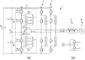
- (A) is a circuit diagram of the power converter device concerning a 1st embodiment
- (b) is a circuit diagram of a chopper cell.
- It is an internal block diagram of the control part of the power converter device concerning a 1st embodiment.
- It is a schematic diagram which shows the control structure of a neutral point electric potential control part. It is a table
- It is a schematic diagram which shows the control structure of the capacitor voltage balance control part between arms.
- It is a schematic diagram which shows the control structure of a chopper cell group output voltage command value production
- FIG. 1 It is a schematic diagram which shows the control structure of an individual capacitor voltage balance control part. It is a figure for demonstrating the voltage output method of a chopper cell.
- A is a figure for demonstrating the conventional MMC
- (b) is a circuit diagram of a chopper cell.
- FIG. 1 is a circuit diagram of the power conversion device of this embodiment
- FIG. 2 is a block diagram of the internal configuration of the control unit of the power conversion device of this embodiment.
- the power conversion device 1 of this embodiment is connected to a DC power supply 20, converts an input DC voltage v_dc into a three-phase AC voltage v_ac, and supplies power via a three-phase transformer 21. AC power is output to the system 22.
- the power conversion apparatus 1 is connected in parallel with a DC power supply 20, and capacitors 2 a and 2 b connected in series to divide the input DC voltage v_dc to create a neutral point potential, in parallel with the DC power supply 20.
- the U-phase, V-phase, and W-phase leg 3 including the chopper cell C that is connected to each other and serves as a unit converter for converting the direct current of the direct current power source 20 into alternating current, and the output voltage of the chopper cell C of each leg 3 are balanced. Therefore, a control unit 5 that controls the circulating current that flows in the leg 3 of each phase is provided.
- the U phase will be described as a representative as appropriate. Further, it is assumed that the following current and voltage are detected by a current detector and a voltage detector (not shown), and the detected values can be input to the control unit 5.
- the power conversion device 1 turns on the switches 31 and 33 and turns on the DC positive terminal in the U-phase leg 3.
- -Switch 31-Chopper cell group circuit 35-Chopper cell group circuit 36-Switch 33-U-phase circulating current that forms a path of DC neutral point N and makes the voltage of the chopper cell C of the chopper cell group circuits 35 and 36 constant from the capacitor 2a Is supplied.
- the switches 32 and 34 are turned on to form a DC neutral point N-switch 32-chopper cell group circuit 35-chopper cell group circuit 36-switch 34-DC negative terminal path.
- the V-phase circulating current and the W-phase circulating current that make the voltage of the chopper cell C of the chopper cell group circuits 35 and 36 constant are supplied from the capacitor 2b.
- the control unit 5 controls the capacitors 2a and 2b to superimpose a neutral point current that keeps the neutral point potential constant on the circulating current of each phase, whereby the potential at the DC neutral point N is superimposed. Is controlled to be constant.
- a neutral point current i is superimposed on the U-phase leg 3 to discharge excess power of the high-voltage capacitor 2a in order to balance the voltage. Shed.
- ⁇ (1 ⁇ 2) i is superimposed in the V-phase leg 3 and the W-phase leg 3 so that the neutral point current i in excess is charged in the low-voltage capacitor 2b. In this way, the capacitors 2a and 2b are balanced, and the neutral point potential is controlled to be constant.
- Capacitors 2 a and 2 b are DC capacitors, connected in series with each other, and arranged in parallel between the positive terminal and the negative terminal of DC power supply 20.
- a DC neutral point N is formed between the capacitors 2a and 2b.
- the reference potential in the present embodiment is a potential at a DC neutral point N created by dividing the input DC voltage v_dc by the capacitors 2a and 2b, and the neutral point potential is approximately 1 ⁇ 2 of the input DC voltage v_dc.
- the capacitor 2a may be referred to as a positive side capacitor 2a and the capacitor 2b may be referred to as a negative side capacitor 2b with reference to the DC neutral point N.
- Capacitors 2a and 2b have smaller capacities than capacitors of chopper cell C described later.
- Each phase leg 3 is connected in parallel with the DC power source 20. Since any leg 3 has the same configuration, the configuration of the U-phase leg 3 will be described as an example.
- the U-phase leg 3 includes switches 31 to 34, chopper cell group circuits 35 and 36 each including a chopper cell C for converting direct current to alternating current, and reactors 37 and 38.
- the switches 31 to 34 are reverse conducting switches composed of a switching element having a self-extinguishing capability such as an IGBT or a MOSFET that allows current to flow in one direction when turned on, and a feedback diode connected in reverse parallel to the switching element. is there.
- the withstand voltages of the switches 31 to 34 are determined by the input DC voltage v_dc of the DC power supply 20.
- the element to be used is determined in consideration of the superposition of the surge voltage at the time of switching to the voltage of v_dc / 2 with respect to the input DC voltage v_dc.
- one element is included for one switch, but a plurality of elements in series with one switch are also referred to as switches 31 to 34.
- the switches 31 to 34 are connected in series between the DC positive terminal and the DC negative terminal in this order.
- the collector (C) of the switch 31 is connected to the DC positive terminal, and the emitter (E) of the switch 34 is connected to the DC negative terminal.
- the emitter (E) of the switch 32 and the collector (C) of the switch 33 are connected to a DC neutral point N divided by the capacitors 2a and 2b.
- a DC circulating current path is formed by turning on and off the switches 31-34.
- the chopper cell group circuits 35 and 36 are configured by connecting N (N ⁇ 1) chopper cells C in series, and convert the DC voltage into a stepped AC voltage using the chopper cell C as a unit converter.
- the chopper cell C is formed by connecting a leg in which switches sw_ch1 and sw_ch2 are connected in series and a DC capacitor c_ch in parallel.
- the configuration of the switches sw_ch1 and sw_ch2 is the same as the configuration of the switches 31 to 34 described above.
- the chopper cell C outputs the voltage v_ch of the DC capacitor c_ch when the switch sw_ch1 is on, and becomes zero voltage when the switch sw_ch2 is on.
- the number of chopper cells C in the chopper cell group circuits 35 and 36 is determined by the input DC voltage v_dc and the chopper cell capacitor voltage v_ch, and is approximately (v_dc / 2) / v_ch. In the present embodiment, the number of chopper cells C is three.
- the positive terminal of the chopper cell group circuit 35 is connected to the collector (C) of the switch 32, and the negative terminal of the chopper cell group circuit 36 is connected to the emitter (E) of the switch 33.
- the negative terminal of the chopper cell group circuit 35 is connected to the output AC voltage terminal via the reactor 37, and the positive terminal of the chopper cell group circuit 36 is connected to the output AC voltage terminal via the reactor 38.
- the chopper cell group circuit 35 is a positive arm connected to the positive side when viewed from the DC side, and may be referred to as an upper arm.
- the chopper cell group circuit 36 is a negative arm connected to the negative side when viewed from the DC side, and may be referred to as a lower arm.
- a reactor 37 is inserted between the chopper cell group circuit 35 and the output AC voltage terminal 39, and a reactor 38 is inserted between the chopper cell group circuit 36 and the output AC voltage terminal 39. ing.
- the control unit 5 controls the circulating current that flows in the leg 3 of each phase in order to make the output voltage of each chopper cell C constant. Therefore, a command to turn on or off is output to the switches 31 to 34 of each phase leg 3 and the switches sw_ch1 and sw_ch2 of the chopper cell C.
- the control unit 5 includes each phase output voltage control unit 51, each phase capacitor voltage balance control unit 52, and a neutral point potential control unit realized by software processing of a computer equipped with a CPU or the like. 53, an inter-arm capacitor voltage balance control unit 54, a circulating current ACR unit 55, a chopper cell group output voltage command value generation unit 56, and an individual capacitor voltage balance control unit 57 are provided.
- the three-phase / DQ conversion unit 511 performs three-phase / DQ conversion on the calculated i_u, i_v, i_w, calculates the D-axis current i_d and the Q-axis current i_q, and outputs them to the ACR unit 512.
- the ACR unit 512 receives the D-axis current i_d, the Q-axis current i_q, and the D-axis current command value i_d * and the Q-axis current command value i_q *, and the D-axis current i_d and the Q-axis current i_q are PI control is performed so as to follow the command value i_d * and the Q-axis current command value i_q *, and the D-axis voltage command value v_d * and the Q-axis voltage command value v_q * are calculated and output to the DQ / 3-phase converter 513. To do.
- the DQ / 3-phase conversion unit 513 performs DQ / 3-phase conversion on the input D-axis voltage command value v_d * and Q-axis voltage command value v_q *, and voltage command values v_u *, v_v *, v_w of each phase. * Is calculated.
- Each phase capacitor voltage balance control unit 52 performs control to keep the average value of the chopper cell group circuits 35 and 36 of each phase constant. Therefore, the U phase will be described as an example.
- the switches 31 and 33 are turned on, and the DC positive terminal—the switch 31—the chopper cell group circuit 35—the chopper cell group circuit 36.
- -A switch 33-a DC circulating current flows through the path of the DC neutral point N.
- the PI control is performed so as to follow the desired command value, and the circulating current command value i_c_u0 * is calculated.
- the same control is performed for the V phase and the W phase, and each phase capacitor voltage control unit 52 outputs the obtained circulating current command values i_c_u0 *, i_c_v0 *, i_c_w0 * of the respective phases to the neutral point potential control unit 53. To do.
- the neutral point potential control unit 53 controls the neutral point potential of the DC neutral point N to be constant.
- the neutral point voltage is kept constant by intentionally flowing the current i_np into the neutral point potential.
- the neutral point current command value i_np * is superimposed on the DC circulating current of each phase.
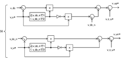
- the neutral point potential control unit 53 includes a neutral point current command value calculation unit 531 and a neutral point current superimposition unit 532, as shown in FIG.
- the neutral point current command value calculation unit 531 receives the input of the voltage v_dc_p of the capacitor 2a and the voltage v_dc_n of the capacitor 2b, calculates a difference voltage between them, and multiplies it by 1/2. Further, the neutral point current command value i_np * is calculated by passing the moving average filter and performing PI control so that the differential voltage follows zero.
- the reason why the difference voltage is halved is that, for example, when the voltage v_dc_p of the capacitor 2a increases, the voltage v_dc_n of the capacitor 2b decreases correspondingly, so that the increased amount can be accurately obtained.
- the moving average filter is provided in order to eliminate the influence on the control. That is, in the three-phase NPC-MMC, the neutral point potential is three times the AC voltage frequency because the current supplied by the positive capacitor 2a and the negative capacitor 2b fluctuates at a frequency three times the AC voltage frequency. Fluctuates. Such harmonic components are included in the voltage difference between the capacitors 2a and 2b, and a moving average is taken in order to eliminate the influence on control such as hunting.
- the moving average cycle is more than the number of legs of the output AC voltage cycle (three times here), so that the influence on the control can be further eliminated.
- harmonic components may be removed by a low-pass filter instead of the moving average filter.
- Increasing the gain means, for example, increasing the gain higher than the gain used in the PI control when at least one of the filters is inserted.
- the neutral point current superimposing unit 532 superimposes the neutral point current command value i_np * obtained by the neutral point current command value calculating unit 531 on the circulating current command value of each phase.
- the U-phase AC voltage is positive, and the V-phase and W-phase AC voltages are negative. Therefore, the U-phase circulating current is supplied from the positive capacitor 2a, and the V and W-phase circulating currents are supplied from the negative capacitor 2b.
- i_np * is added to the U-phase circulating current command value i_c_u0 *, and the V and W-phase circulating current command values i_c_v0 *, i_np * / 2 is distributed and subtracted from i_c_w0 *.
- the circulating current command values i_c_u1 *, i_c_v1 *, i_c_w1 * for each phase for making the neutral point potential constant are calculated.
- the neutral point voltage can be made constant by the same control method.
- the neutral point potential control unit 53 outputs the circulating current command values i_c_u1 *, i_c_v1 *, i_c_w1 * of each phase for making the obtained neutral point potential constant to the inter-arm capacitor voltage control unit 54.
- the inter-arm capacitor voltage balance control unit 54 makes the capacitor voltage average value v_ch_up of the chopper cell group circuit 35 and the capacitor voltage average value v_ch_un of the chopper cell group circuit 36 the same. To realize this, when the output AC voltage is larger than the DC neutral point voltage, the output is made to the path of DC positive terminal-switch 31-chopper cell group circuit 35-chopper cell group circuit 36-switch 33-DC neutral point N. An AC circulating current with the same frequency as the AC voltage is applied. When the output AC voltage is smaller than the DC neutral point voltage, the DC neutral point N-switch 32-chopper cell group circuit 35-chopper cell group circuit 36-switch 34-DC negative terminal has the same frequency as the output AC voltage. Apply AC circulating current.
- the capacitor voltage average value v_ch_up of the upper arm 35 and the capacitor voltage average value v_ch_un of the lower arm 36 are received, and the value obtained by subtracting v_ch_un from v_ch_up and substituting the value for proportional integration control is substituted into the sine function.
- the obtained value is set as an AC circulating current command value i_c_ac *.
- the U-phase circulating current command value i_c_u * is calculated by adding this and the U-phase circulating current command value i_c_u1 * for making the neutral point potential constant. Therefore, the U-phase circulating current command value i_c_u * is obtained by adding the AC circulating current to the DC circulating current.
- the inter-arm capacitor voltage control unit 54 calculates the circulating current command values for the V phase and the W phase, and outputs the calculated phase circulating current command values i_c_u *, i_c_v *, i_c_w * to the circulating current ACR unit 55. To do.
- the circulating current ACR unit 55 performs proportional-integral control so that the U-phase circulating current i_c_u follows the input U-phase circulating current command value i_c_u *, and generates a U-phase circulating voltage command value v_c_u *. Similarly, the circulating current ACR 55 is generated for the V phase and the W phase, and the circulating voltage command values v_c_u *, v_c_v *, and v_c_w * of each phase are output to the chopper cell group output voltage command value generation unit 56.
- the chopper cell group output voltage command value generation unit 56 generates voltage command values output from the chopper cell group circuits 35 and 36.
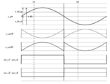
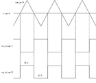
- FIG. 6 by taking the U phase as an example, when the AC voltage command value v_u * is greater than the DC neutral point voltage v_dc_n, as shown at timing t1 in FIG. Turn off.
- the chopper cell group circuit 35 outputs a difference voltage between the input DC voltage v_dc and the output AC voltage v_ac_u
- the chopper cell group circuit 36 outputs a difference voltage between the output AC voltage v_ac_u and the DC neutral point voltage v_dc_n.
- the switches 32 and 34 are turned on and the switches 31 and 33 are turned off.
- the chopper cell group circuit 35 outputs a difference voltage between the DC neutral point voltage v_dc_n and the output AC voltage v_ac_u
- the chopper cell group circuit 36 outputs a difference voltage between the output AC voltage v_ac_u and the DC negative voltage.
- v_up * v_dc_n ⁇ v_u * ⁇ v_c_u *.
- v_un * v_u * ⁇ v_c_u *.
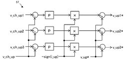
- the individual capacitor voltage balance control unit 57 adjusts the output voltages of the chopper cells C of the chopper cell group circuits 35 and 36 to be the same. That is, since the capacitor is charged when the U-phase upper arm current i_up is positive, the output voltage of the chopper cell C having a small capacitor voltage is increased, and the output voltage of the chopper cell C having a large capacitor voltage is decreased. Since the capacitor is discharged when the U-phase upper arm current i_up is negative, the output voltage of the chopper cell C having a small capacitor voltage is decreased, and the output voltage of the chopper cell C having a large capacitor voltage is increased.
- the individual capacitor voltage balance control unit 57 will be described by taking the U-phase chopper cell group circuit 35 as an example.
- the capacitor voltage of the chopper cell group circuit 35 is obtained from the capacitor voltage v_ch_up1.
- the value obtained by subtracting the voltage average value v_ch_up and multiplying this by the proportional gain is multiplied by a value ⁇ sign (i_up) obtained by inverting the sign of the U-phase arm current i_up, and the U-phase arm voltage command value v_up * is added.
- the voltage command values v_up1 *, v_up2 *, and v_up3 * of each chopper cell are calculated.
- a chopper cell ch_up1 will be described as an example with reference to FIG. Note that the two switches constituting the chopper cell ch_up1 are sw_ch_up11 and sw_ch_up12.
- the switch sw_ch_up11 is turned on and the sw_ch_up12 is turned off.
- the switch sw_ch_up11 is turned off and the sw_ch_up12 is turned on.
- the equivalent carrier frequency can be increased to N times the carrier triangular wave frequency by shifting the phase of the carrier triangular wave by 360 ° / N, and each switch can be turned on and off more. Do it finely. Therefore, the harmonic voltage of the output AC voltage can be reduced and the output AC voltage can be made smooth. Further, by making the carrier triangular wave phase used for the chopper cell group circuit 36 the same as that of the chopper cell group circuit 35, the harmonic voltage of the output AC voltage can be further reduced.
- the power conversion device 1 of the present embodiment is a power conversion device that converts power between alternating current and direct current, and is connected in parallel with the direct current power source 20 to divide the input direct current voltage of the direct current power source 20.
- Capacitors 2a and 2b connected in series for generating a neutral point potential, a plurality of legs 3 each connected in parallel with a DC power supply 20 and including a chopper cell C for converting DC to AC, and a leg for each phase 3 to control the circulating current that flows in the leg 3 of each phase in order to balance the output voltage of the three chopper cells, and the control unit 5
- a neutral point potential control unit 53 for superimposing a neutral point current for controlling the neutral point potential to be constant is provided, and the neutral point potential control unit 53 is connected to at least one of the capacitors 2a and 2b. Circulated current superimposed on
- the neutral point clamp type power converter that can keep the neutral point potential constant.
- a method of applying a zero-phase voltage is also conceivable, but in this case, the control response speed depends on the frequency of the output AC voltage, resulting in neutral point potential fluctuations. There is a risk of increasing the DC capacitor capacity.
- the neutral point current can be flowed at any time during one period, so that a control response speed independent of the frequency of the output AC voltage can be realized.
- the leg 3 includes multiple switches 31 to 34 connected in series and a pair of chopper cell group circuits 35 and 36 in which one or more chopper cells C are connected in series. In this order, it is provided between a DC positive terminal and a DC negative terminal connected to the DC power supply 20, and is connected to the DC neutral point N between the switch 32 and the switch 33. 32 and 33 are connected in parallel.
- the number of chopper cells can be reduced to half, and the size of the power converter can be reduced.
- the DC capacitor capacity is smaller than that of the chopper cell, and the size of the power converter can be reduced.
- switching loss can be reduced and conversion efficiency can be improved by reducing the number of chopper cells.
- the neutral point potential control unit 53 charges the low-voltage capacitor with the power discharged from the high-voltage capacitor among the capacitors 2a and 2b. Thereby, it is possible to easily control the neutral point potential to be constant. For example, when the positive side capacitor 2a has a high voltage and the negative side capacitor 2b has a low voltage, the discharge current of the positive side capacitor 2a is charged to the negative side capacitor 2b via the other two-phase leg 3, and the capacitor 2a , 2b, it is easier to keep the neutral point potential constant by controlling both capacitors 2a, 2b.
- the neutral point potential control unit 53 distributes and superimposes the neutral point current to the leg 3 of each phase.
- the neutral point current to be superimposed is distributed to the leg 3 of each phase, so that it is possible to reduce a burden such as a thermal burden accompanying an increase in the current flowing through the switches 31 to 34.
- a burden such as a thermal burden accompanying an increase in the current flowing through the switches 31 to 34.
- a neutral point current is allowed to flow only in the U-phase leg 3
- the positive capacitor 2 a is discharged and charged in the capacitor of the chopper cell group circuit 35, and the V-phase and W-phase leg 3 is charged.
- the burden can be distributed to each phase leg 3.
- the neutral point potential control unit 53 calculates the neutral point current command value i_np * by proportional-integral control of the voltage difference between the capacitors 2a and 2b. Thereby, the voltages of the capacitors 2a and 2b become the same, and the neutral point potential can be controlled to be constant.
- the neutral point potential control unit 53 includes a low-pass filter that removes a high-frequency component included in the voltage difference between the capacitors 2a and 2b. As a result, a stable neutral point current command value can be generated, so that it is possible to eliminate the influence on control due to having a high-frequency component.
- the neutral point potential control unit 53 has a moving average filter that removes high frequency components included in the voltage difference between the capacitors 2a and 2b. As a result, a stable neutral point current command value can be generated, so that it is possible to eliminate the influence on control due to having a high-frequency component.
- the moving average period of the moving average filter is set to be not less than the number of legs of the output AC voltage period.
- the neutral point potential is formed by the two capacitors 2a and 2b.
- the neutral point potential is determined by a capacitor connected in series on the positive side and a capacitor connected in series on the negative side. You may make it form. Thereby, a withstand voltage can be enlarged. Further, two or more capacitors may be connected in parallel to each of the capacitors 2a and 2b to increase the capacitor capacity.
- the three-phase legs 3 are connected in parallel to the two capacitors 2a and 2b connected in series.
- the two capacitors 2a connected in series to the leg 3 in each phase are connected.
- 2b may be connected in parallel most recently.
Abstract
A power conversion device that can keep a neutral potential constant is provided. Said power conversion device, which converts power between AC and DC, is provided with the following: series-connected capacitors 2a, 2b that are connected in parallel with a DC power supply 20 and divide an input DC voltage therefrom so as to create a neutral potential; a plurality of legs 3 that are each connected in parallel with the DC power supply 20 and that contain chopper cells C for converting DC to AC; and a control unit that controls circulating currents that are made to flow through the legs 3 for the respective phases in order to balance the chopper-cell output voltages in the respective legs 3. The control unit contains a neutral-potential control unit that superimposes, onto the DC circulating current made to flow between DC terminals for each phase, a neutral current for keeping the abovementioned neutral potential constant. Said neutral-potential control unit makes at least one of the abovementioned capacitors 2a, 2b circulate the circulating currents with the aforementioned neutral currents superimposed thereupon.
Description
本発明の実施形態は、直流と交流との間で相互に電力を変換する電力変換装置に関する。
Embodiment of this invention is related with the power converter device which converts electric power mutually between direct current | flow and alternating current.
近年、風力発電や太陽光発電、太陽熱発電などの再生可能エネルギーの普及が促進されているが、より大電力を再生可能エネルギーで賄うために、洋上風力発電や、砂漠地帯での太陽光、太陽熱発電が検討され始めている。洋上風力発電においては、発電された電力を消費地である都市まで海底ケーブルで大電力送電したり、アフリカや中国奥部の砂漠地帯から、ヨーロッパや沿岸地帯の大都市まで大電力を長距離にわたって高効率に送電したりすることが必要になる。このような要求には、従来の三相交流による電力送電よりも、直流送電のほうが高効率で、コストを抑えながら設置することが可能になるため、直流送電網の構築が検討され始めている。
In recent years, the spread of renewable energy such as wind power generation, solar power generation, and solar thermal power generation has been promoted, but in order to cover more power with renewable energy, offshore wind power generation, solar power in the desert area, solar heat Power generation is being considered. In offshore wind power generation, the generated power is transmitted to the city where it is consumed using a submarine cable, or the power is generated over a long distance from the desert area in the back of Africa or China to a large city in Europe or the coastal area. It is necessary to transmit power with high efficiency. In order to meet such demand, DC power transmission is more efficient than conventional three-phase AC power transmission, and it can be installed with reduced costs. Therefore, construction of a DC power transmission network has begun to be studied.
直流送電においては、発電された交流電力を直流送電用の直流に変換するコンバータや、送電されてきた直流を都市内の交流に変換するインバータなどの電力変換装置が必要になる。交流系統にコンバータ、インバータのスイッチングに伴う高調波が流出しないように、正弦波に近い電圧波形を出力することができ、出力フィルタを削減できるMMC(モジュラーマルチレベルコンバータ)が実用化されている。
DC power transmission requires a power converter such as a converter that converts the generated AC power into DC for DC power transmission and an inverter that converts the transmitted DC power into city AC. An MMC (modular multi-level converter) that can output a voltage waveform close to a sine wave and reduce output filters has been put into practical use so that harmonics accompanying switching of the converter and inverter do not flow into the AC system.
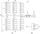
従来の直流送電用途に使用されるMMCの一例を図10に示す。図10(a)に示すように、MMC101は、直流電源120とそれぞれ並列に接続された交流電圧を生成するU相、V相及びW相レグ103を備える。各レグ103は、生成した交流電圧を所望の交流電圧に変換する三相トランス121と接続され、この三相トランス121が電力系統122と接続されている。
An example of an MMC used for conventional DC power transmission is shown in FIG. As shown in FIG. 10A, the MMC 101 includes U-phase, V-phase, and W-phase legs 103 that generate AC voltages connected in parallel with the DC power source 120, respectively. Each leg 103 is connected to a three-phase transformer 121 that converts the generated AC voltage into a desired AC voltage, and this three-phase transformer 121 is connected to the power system 122.
各相のレグ103の構成は何れも同様であるため、U相レグ103について説明すると、U相レグ103は、入力直流電圧から交流電圧を生成するための手段であり、直列接続された12個のチョッパセルCを有している。すなわち、U相レグ103は、チョッパセルCが6つ直列接続されてなる正側の上アーム104aと、チョッパセルCが6つ直列接続されてなる負側の下アーム104bとからなる。
Since the configuration of each phase leg 103 is the same, the U-phase leg 103 will be described. The U-phase leg 103 is a means for generating an AC voltage from an input DC voltage, and is connected in series to 12 pieces. The chopper cell C is provided. That is, the U-phase leg 103 includes a positive upper arm 104a in which six chopper cells C are connected in series, and a negative lower arm 104b in which six chopper cells C are connected in series.
上アーム104a及び下アーム104bの間には、三相トランス121と接続される交流出力端子139が設けられ、上アーム104a及び端子139の間にリアクトルlb_upが配置され、下アーム104b及び端子139の間にリアクトルlb_unが配置されている。チョッパセルCは、図10(b)に示すように、自己消弧能力を備える2つのスイッチsw_ch1,sw_ch2が直列接続されてなるレグ105と、レグ105に並列接続されたコンデンサc_chとから構成される。チョッパセルCは、コンデンサc_chを直流電圧源として、スイッチsw_ch1がオン時にコンデンサc_chの電圧v_chを出力し、スイッチsw_ch2がオン時にチョッパセルCの両端子が同電位となる。チョッパセルCが多直列接続されたU相レグ103は、各チョッパセルCへのスイッチングのタイミングをずらすことにより、多段の階段状の交流電圧波形を生成する。
An AC output terminal 139 connected to the three-phase transformer 121 is provided between the upper arm 104a and the lower arm 104b, a reactor lb_up is disposed between the upper arm 104a and the terminal 139, and the lower arm 104b and the terminal 139 A reactor lb_un is arranged between them. As shown in FIG. 10B, the chopper cell C includes a leg 105 in which two switches sw_ch1 and sw_ch2 having a self-extinguishing capability are connected in series, and a capacitor c_ch connected in parallel to the leg 105. . The chopper cell C uses the capacitor c_ch as a DC voltage source, outputs the voltage v_ch of the capacitor c_ch when the switch sw_ch1 is on, and both terminals of the chopper cell C have the same potential when the switch sw_ch2 is on. The U-phase leg 103 in which the chopper cells C are connected in series generates a multi-step AC voltage waveform by shifting the switching timing to each chopper cell C.
このMMC101の動作についてU相レグ103を例に説明すると、直流電源120の入力直流電圧v_dcから正側チョッパセルch_up1~6の合計電圧v_upを減算し、基準電位から負側チョッパセルch_un1~6の合計電圧v_unを加算することによって交流電圧が得られ、さらに三相トランス121で所望の交流電圧に変換される。
The operation of the MMC 101 will be described by taking the U-phase leg 103 as an example. The total voltage v_up of the positive chopper cells ch_up1 to 6 is subtracted from the input DC voltage v_dc of the DC power supply 120, and the total voltage of the negative chopper cells ch_un1 to 6 is subtracted from the reference potential. An alternating voltage is obtained by adding v_un, and is further converted into a desired alternating voltage by the three-phase transformer 121.
また、リアクトルlb_up及びlb_unによって、入力直流電圧v_dcとチョッパセル出力電圧v_up+v_unの短絡による電流の増大が抑制される。V相レグ103及びW相レグ103についても同様である。
Also, the reactors lb_up and lb_un suppress an increase in current due to a short circuit between the input DC voltage v_dc and the chopper cell output voltage v_up + v_un. The same applies to the V-phase leg 103 and the W-phase leg 103.
以上説明した動作により、三相交流電圧を生成し、三相トランス121によって所望の交流電圧に変換し、電力系統122に三相交流電圧を供給する。
Through the operation described above, a three-phase AC voltage is generated, converted into a desired AC voltage by the three-phase transformer 121, and the three-phase AC voltage is supplied to the power system 122.
MMCは、チョッパセルのコンデンサに出力交流周波数と同等の電力脈動が原理的に生じる。このコンデンサ電圧の変動を一定の値に抑制するためには、コンデンサの容量を大きくする必要があり、装置自体が大きくなってしまっていた。例えば、直流電圧が数十kV~数百kVに及ぶ直流送電の場合、チョッパセルの数が多くなり、それに比例してコンデンサ体積が大きくなり、電力変換装置の体積が大きくなってしまう。
In MMC, in principle, power pulsation equivalent to the output AC frequency occurs in the capacitor of the chopper cell. In order to suppress the fluctuation of the capacitor voltage to a constant value, it is necessary to increase the capacity of the capacitor, and the apparatus itself has become large. For example, in the case of DC power transmission in which the DC voltage reaches several tens of kV to several hundreds of kV, the number of chopper cells increases, the capacitor volume increases proportionally, and the volume of the power converter increases.
そこで、IGBT等の自励式スイッチング素子とこれに逆接続したダイオードからなるスイッチ(バルブ)と、チョッパセルとを組み合わせた中性点クランプ形モジュラー・マルチレベル・コンバータ(以下、NPC-MMCという。)が検討され始めている。このNPC-MMCは、直流電源の入力直流電圧を例えば2つのコンデンサで半分に分割し、コンデンサ間に中性点電位を形成する。すなわち、入力直流電圧に対し、直列接続した2つのコンデンサを並列に接続する。NPC-MMCは、各チョッパセルの動作タイミングをずらすことで階段状のマルチレベル電圧波形を出力でき、出力交流電圧をほぼ正弦波にできるというMMCの利点を受け継ぎつつ、チョッパセル数が減少できるので、電力変換装置の設置スペースを低減できる可能性がある。
Therefore, a neutral point clamped modular multi-level converter (hereinafter referred to as NPC-MMC) that combines a switch (valve) composed of a self-excited switching element such as an IGBT and a diode reversely connected thereto and a chopper cell. Being considered. The NPC-MMC divides an input DC voltage of a DC power source into halves by, for example, two capacitors, and forms a neutral point potential between the capacitors. That is, two capacitors connected in series are connected in parallel to the input DC voltage. NPC-MMC can output a stepped multi-level voltage waveform by shifting the operation timing of each chopper cell, and can reduce the number of chopper cells while inheriting the advantage of MMC that the output AC voltage can be made almost sinusoidal. There is a possibility that the installation space for the conversion device can be reduced.
ところが、中性点電位はコンデンサやスイッチング素子の漏れ電流、放電電流の不平衡により変動してしまう。そのため、例えば、正側のコンデンサと負側のコンデンサの放電電圧のバランスが崩れて、スイッチング素子に耐電圧を超えた電圧が印加され、スイッチング素子が故障し、その結果電力変換装置自体の故障に繋がる虞があった。
However, the neutral point potential fluctuates due to the unbalanced leakage current and discharge current of the capacitor and switching element. For this reason, for example, the discharge voltage of the positive capacitor and the negative capacitor are unbalanced, a voltage exceeding the withstand voltage is applied to the switching element, and the switching element fails, resulting in failure of the power converter itself. There was a risk of being connected.
本発明の実施形態に係る電力変換装置は、上記のような課題を解決するためになされたものであり、中性点電位を一定に保つことのできる電力変換装置を提供することを目的とする。
The power conversion device according to the embodiment of the present invention is made to solve the above-described problems, and an object thereof is to provide a power conversion device capable of keeping the neutral point potential constant. .
上記の目的を達成するために、本実施形態の電力変換装置は、交流と直流の間で電力を変換する電力変換装置であって、直流電源と並列に接続され、前記直流電源の入力直流電圧を分割して中性点電位を作るための直列接続された第1及び第2のコンデンサと、前記直流電源と並列に各々接続され、直流を交流に変換するためのチョッパセルを含む複数のレグと、各相のレグの前記チョッパセル出力電圧をバランスさせるために各相のレグ内に流す循環電流を制御する制御部と、を備え、前記制御部は、各相の直流端子間に流す直流循環電流に、中性点電位を一定に制御するための中性点電流を重畳する中性点電位制御部を有し、前記中性点電位制御部は、前記第1及び第2のコンデンサの少なくとも何れかに前記中性点電流を重畳した循環電流を流させること、を特徴とする。
In order to achieve the above object, a power conversion device according to the present embodiment is a power conversion device that converts power between alternating current and direct current, and is connected in parallel with a direct current power source, and an input direct current voltage of the direct current power source. First and second capacitors connected in series for generating a neutral point potential, and a plurality of legs each connected in parallel to the DC power source and including a chopper cell for converting DC to AC A control unit that controls a circulating current that flows in the legs of each phase in order to balance the output voltage of the chopper cell of each phase leg, and the control unit passes a DC circulating current that flows between the DC terminals of each phase A neutral point potential control unit that superimposes a neutral point current for controlling the neutral point potential to be constant, and the neutral point potential control unit includes at least one of the first and second capacitors. A circuit in which the neutral point current is superimposed. Causing current flows, characterized by.
[1.第1の実施形態]
[1-1.概略構成]
以下では、図1~図9を参照しつつ、本実施形態の電力変換装置について説明する。図1は、本実施形態の電力変換装置の回路図であり、図2は、本実施形態の電力変換装置の制御部の内部構成ブロック図である。 [1. First Embodiment]
[1-1. Schematic configuration]
Hereinafter, the power conversion device of the present embodiment will be described with reference to FIGS. 1 to 9. FIG. 1 is a circuit diagram of the power conversion device of this embodiment, and FIG. 2 is a block diagram of the internal configuration of the control unit of the power conversion device of this embodiment.
図1(a)に示すように、本実施形態の電力変換装置1は、直流電源20と接続され、入力直流電圧v_dcを三相の交流電圧v_acに変換し、三相トランス21を介して電力系統22に交流電力を出力するものである。
As shown in FIG. 1A, the power conversion device 1 of this embodiment is connected to a DC power supply 20, converts an input DC voltage v_dc into a three-phase AC voltage v_ac, and supplies power via a three-phase transformer 21. AC power is output to the system 22.
本電力変換装置1は、直流電源20と並列に接続され、その入力直流電圧v_dcを分割して中性点電位を作るための互いに直列接続されたコンデンサ2a,2bと、直流電源20と並列に各々接続され、直流電源20の直流を交流に変換するための単位変換器となるチョッパセルCを含むU相、V相及びW相のレグ3と、各レグ3のチョッパセルCの出力電圧をバランスさせるために各相のレグ3内に流す循環電流を制御する制御部5と、を備える。
The power conversion apparatus 1 is connected in parallel with a DC power supply 20, and capacitors 2 a and 2 b connected in series to divide the input DC voltage v_dc to create a neutral point potential, in parallel with the DC power supply 20. The U-phase, V-phase, and W-phase leg 3 including the chopper cell C that is connected to each other and serves as a unit converter for converting the direct current of the direct current power source 20 into alternating current, and the output voltage of the chopper cell C of each leg 3 are balanced. Therefore, a control unit 5 that controls the circulating current that flows in the leg 3 of each phase is provided.
なお、U相、V相、W相の電力変換装置の構成は同じであるので、適宜代表してU相について説明する。また、以下に示す電流、電圧は、不図示の電流検出器及び電圧検出器によって検出され、その検出値が制御部5に入力可能に構成されていることを前提とする。
Since the configurations of the U-phase, V-phase, and W-phase power converters are the same, the U phase will be described as a representative as appropriate. Further, it is assumed that the following current and voltage are detected by a current detector and a voltage detector (not shown), and the detected values can be input to the control unit 5.
本電力変換装置1は、例えば、U相交流電圧が正、V相交流電圧及びW相交流電圧が負である場合、U相レグ3においては、スイッチ31,33をオンにして、直流正端子-スイッチ31-チョッパセル群回路35-チョッパセル群回路36-スイッチ33-直流中性点Nの経路を形成し、コンデンサ2aからチョッパセル群回路35,36のチョッパセルCの電圧を一定にするU相循環電流が供給される。V相レグ3及びW相レグ3においては、スイッチ32,34をオンにして、直流中性点N-スイッチ32-チョッパセル群回路35-チョッパセル群回路36-スイッチ34-直流負端子の経路を形成し、コンデンサ2bからチョッパセル群回路35,36のチョッパセルCの電圧を一定にするV相循環電流及びW相循環電流が供給される。
For example, when the U-phase AC voltage is positive and the V-phase AC voltage and the W-phase AC voltage are negative, the power conversion device 1 turns on the switches 31 and 33 and turns on the DC positive terminal in the U-phase leg 3. -Switch 31-Chopper cell group circuit 35-Chopper cell group circuit 36-Switch 33-U-phase circulating current that forms a path of DC neutral point N and makes the voltage of the chopper cell C of the chopper cell group circuits 35 and 36 constant from the capacitor 2a Is supplied. In the V-phase leg 3 and the W-phase leg 3, the switches 32 and 34 are turned on to form a DC neutral point N-switch 32-chopper cell group circuit 35-chopper cell group circuit 36-switch 34-DC negative terminal path. Then, the V-phase circulating current and the W-phase circulating current that make the voltage of the chopper cell C of the chopper cell group circuits 35 and 36 constant are supplied from the capacitor 2b.
本実施形態では、制御部5により、コンデンサ2a,2bを制御して、各相の循環電流に中性点電位を一定にする中性点電流を重畳させることにより、直流中性点Nの電位を一定に制御する。例えば、コンデンサ2aの電圧がコンデンサ2bの電圧よりも大きい場合、バランスを取るために、高電圧なコンデンサ2aの余分な電力を放電させるために中性点電流iを重畳させてU相レグ3内に流す。一方、V相レグ3及びW相レグ3内に-(1/2)iを重畳させて、余分な分の中性点電流iが低電圧なコンデンサ2bに充電されるようにする。このようにして、コンデンサ2a,2bのバランスを図り、中性点電位を一定に制御する。
In the present embodiment, the control unit 5 controls the capacitors 2a and 2b to superimpose a neutral point current that keeps the neutral point potential constant on the circulating current of each phase, whereby the potential at the DC neutral point N is superimposed. Is controlled to be constant. For example, when the voltage of the capacitor 2a is larger than the voltage of the capacitor 2b, a neutral point current i is superimposed on the U-phase leg 3 to discharge excess power of the high-voltage capacitor 2a in order to balance the voltage. Shed. On the other hand, − (½) i is superimposed in the V-phase leg 3 and the W-phase leg 3 so that the neutral point current i in excess is charged in the low-voltage capacitor 2b. In this way, the capacitors 2a and 2b are balanced, and the neutral point potential is controlled to be constant.
[1-2.詳細構成]
[コンデンサ]
コンデンサ2a,2bは、直流コンデンサであり、互いに直列接続されて、直流電源20の正端子及び負端子間に並列に配置されている。両コンデンサ2a,2b間には直流中性点Nが形成されている。本実施形態における基準電位は、入力直流電圧v_dcをコンデンサ2a,2bで分割して作られる直流中性点Nの電位とし、中性点電位は、入力直流電圧v_dcの概1/2である。直流中性点Nを基準としてコンデンサ2aを正側コンデンサ2a、コンデンサ2bを負側コンデンサ2bと呼ぶ場合がある。なお、コンデンサ2a,2bは、後述のチョッパセルCのコンデンサより容量が小さい。 [1-2. Detailed configuration]
[Capacitor]
Capacitors 2 a and 2 b are DC capacitors, connected in series with each other, and arranged in parallel between the positive terminal and the negative terminal of DC power supply 20. A DC neutral point N is formed between the capacitors 2a and 2b. The reference potential in the present embodiment is a potential at a DC neutral point N created by dividing the input DC voltage v_dc by the capacitors 2a and 2b, and the neutral point potential is approximately ½ of the input DC voltage v_dc. The capacitor 2a may be referred to as a positive side capacitor 2a and the capacitor 2b may be referred to as a negative side capacitor 2b with reference to the DC neutral point N. Capacitors 2a and 2b have smaller capacities than capacitors of chopper cell C described later.
[コンデンサ]
コンデンサ2a,2bは、直流コンデンサであり、互いに直列接続されて、直流電源20の正端子及び負端子間に並列に配置されている。両コンデンサ2a,2b間には直流中性点Nが形成されている。本実施形態における基準電位は、入力直流電圧v_dcをコンデンサ2a,2bで分割して作られる直流中性点Nの電位とし、中性点電位は、入力直流電圧v_dcの概1/2である。直流中性点Nを基準としてコンデンサ2aを正側コンデンサ2a、コンデンサ2bを負側コンデンサ2bと呼ぶ場合がある。なお、コンデンサ2a,2bは、後述のチョッパセルCのコンデンサより容量が小さい。 [1-2. Detailed configuration]
[Capacitor]
[レグ]
各相のレグ3は、直流電源20とそれぞれ並列に接続されている。何れのレグ3も同様の構成であるので、U相レグ3の構成を例に説明する。U相レグ3は、スイッチ31~34と、直流を交流に変換するためのチョッパセルCを備えたチョッパセル群回路35,36と、リアクトル37,38とを有している。 [Leg]
Eachphase leg 3 is connected in parallel with the DC power source 20. Since any leg 3 has the same configuration, the configuration of the U-phase leg 3 will be described as an example. The U-phase leg 3 includes switches 31 to 34, chopper cell group circuits 35 and 36 each including a chopper cell C for converting direct current to alternating current, and reactors 37 and 38.
各相のレグ3は、直流電源20とそれぞれ並列に接続されている。何れのレグ3も同様の構成であるので、U相レグ3の構成を例に説明する。U相レグ3は、スイッチ31~34と、直流を交流に変換するためのチョッパセルCを備えたチョッパセル群回路35,36と、リアクトル37,38とを有している。 [Leg]
Each
(スイッチ)
スイッチ31~34は、オン時には電流を一方向に流すIGBTやMOSFET等の自己消弧能力を有するスイッチング素子と、このスイッチング素子に逆並列に接続された帰還ダイオードとで構成される逆導通スイッチである。スイッチ31~34は、直流電源20の入力直流電圧v_dcにより耐電圧が決定される。入力直流電圧v_dcに対して、v_dc/2の電圧にスイッチング時のサージ電圧の重畳を考慮し、使用する素子を決定する。直流電圧が数十kV以上に及ぶと、1素子で耐電圧を持たせることは困難になり、複数の素子を直列にする必要がある。本実施形態では1つのスイッチに対し1素子を含むが、1つのスイッチに複数の素子を直列にする場合もスイッチ31~34と称する。 (switch)
Theswitches 31 to 34 are reverse conducting switches composed of a switching element having a self-extinguishing capability such as an IGBT or a MOSFET that allows current to flow in one direction when turned on, and a feedback diode connected in reverse parallel to the switching element. is there. The withstand voltages of the switches 31 to 34 are determined by the input DC voltage v_dc of the DC power supply 20. The element to be used is determined in consideration of the superposition of the surge voltage at the time of switching to the voltage of v_dc / 2 with respect to the input DC voltage v_dc. When the DC voltage reaches several tens of kV or more, it becomes difficult to provide a withstand voltage with one element, and it is necessary to connect a plurality of elements in series. In the present embodiment, one element is included for one switch, but a plurality of elements in series with one switch are also referred to as switches 31 to 34.
スイッチ31~34は、オン時には電流を一方向に流すIGBTやMOSFET等の自己消弧能力を有するスイッチング素子と、このスイッチング素子に逆並列に接続された帰還ダイオードとで構成される逆導通スイッチである。スイッチ31~34は、直流電源20の入力直流電圧v_dcにより耐電圧が決定される。入力直流電圧v_dcに対して、v_dc/2の電圧にスイッチング時のサージ電圧の重畳を考慮し、使用する素子を決定する。直流電圧が数十kV以上に及ぶと、1素子で耐電圧を持たせることは困難になり、複数の素子を直列にする必要がある。本実施形態では1つのスイッチに対し1素子を含むが、1つのスイッチに複数の素子を直列にする場合もスイッチ31~34と称する。 (switch)
The
スイッチ31~34は、直流正端子及び直流負端子間にこの順に直列接続されている。直流正端子にはスイッチ31のコレクタ(C)が接続され、直流負端子にはスイッチ34のエミッタ(E)が接続されている。スイッチ32のエミッタ(E)及びスイッチ33のコレクタ(C)がコンデンサ2a,2bにより分割される直流中性点Nに接続されている。スイッチ31~34のオンオフによって、直流循環電流の経路を形成する。
The switches 31 to 34 are connected in series between the DC positive terminal and the DC negative terminal in this order. The collector (C) of the switch 31 is connected to the DC positive terminal, and the emitter (E) of the switch 34 is connected to the DC negative terminal. The emitter (E) of the switch 32 and the collector (C) of the switch 33 are connected to a DC neutral point N divided by the capacitors 2a and 2b. A DC circulating current path is formed by turning on and off the switches 31-34.
(チョッパセル群回路)
チョッパセル群回路35,36は、N個(N≧1)のチョッパセルCを直列接続して構成されており、チョッパセルCを単位変換器として直流電圧を階段状の交流電圧に変換する。チョッパセルCは、図1(b)に示すように、スイッチsw_ch1,sw_ch2を直列接続したレグと、直流コンデンサc_chとを並列接続してなる。スイッチsw_ch1,sw_ch2の構成は、前述のスイッチ31~34の構成と同様である。チョッパセルCは、スイッチsw_ch1がオン時に直流コンデンサc_chの電圧v_chを出力し、スイッチsw_ch2がオン時にゼロ電圧となる。チョッパセル群回路35,36のチョッパセルC数は、入力直流電圧v_dcと、チョッパセルコンデンサ電圧v_chによって決定され、概ね(v_dc/2)/v_chである。本実施形態では、チョッパセルC数を3としている。 (Chopper cell group circuit)
The chopper cell group circuits 35 and 36 are configured by connecting N (N ≧ 1) chopper cells C in series, and convert the DC voltage into a stepped AC voltage using the chopper cell C as a unit converter. As shown in FIG. 1B, the chopper cell C is formed by connecting a leg in which switches sw_ch1 and sw_ch2 are connected in series and a DC capacitor c_ch in parallel. The configuration of the switches sw_ch1 and sw_ch2 is the same as the configuration of the switches 31 to 34 described above. The chopper cell C outputs the voltage v_ch of the DC capacitor c_ch when the switch sw_ch1 is on, and becomes zero voltage when the switch sw_ch2 is on. The number of chopper cells C in the chopper cell group circuits 35 and 36 is determined by the input DC voltage v_dc and the chopper cell capacitor voltage v_ch, and is approximately (v_dc / 2) / v_ch. In the present embodiment, the number of chopper cells C is three.
チョッパセル群回路35,36は、N個(N≧1)のチョッパセルCを直列接続して構成されており、チョッパセルCを単位変換器として直流電圧を階段状の交流電圧に変換する。チョッパセルCは、図1(b)に示すように、スイッチsw_ch1,sw_ch2を直列接続したレグと、直流コンデンサc_chとを並列接続してなる。スイッチsw_ch1,sw_ch2の構成は、前述のスイッチ31~34の構成と同様である。チョッパセルCは、スイッチsw_ch1がオン時に直流コンデンサc_chの電圧v_chを出力し、スイッチsw_ch2がオン時にゼロ電圧となる。チョッパセル群回路35,36のチョッパセルC数は、入力直流電圧v_dcと、チョッパセルコンデンサ電圧v_chによって決定され、概ね(v_dc/2)/v_chである。本実施形態では、チョッパセルC数を3としている。 (Chopper cell group circuit)
The chopper
チョッパセル群回路35は、その正端子がスイッチ32のコレクタ(C)と接続され、チョッパセル群回路36は、その負端子がスイッチ33のエミッタ(E)と接続されている。また、チョッパセル群回路35の負端子がリアクトル37を介して出力交流電圧端子と接続され、チョッパセル群回路36の正端子がリアクトル38を介して出力交流電圧端子と接続されている。
The positive terminal of the chopper cell group circuit 35 is connected to the collector (C) of the switch 32, and the negative terminal of the chopper cell group circuit 36 is connected to the emitter (E) of the switch 33. The negative terminal of the chopper cell group circuit 35 is connected to the output AC voltage terminal via the reactor 37, and the positive terminal of the chopper cell group circuit 36 is connected to the output AC voltage terminal via the reactor 38.
なお、チョッパセル群回路35は、直流側から見て正側に接続された正側のアームであり、上アームと呼ぶ場合がある。また、チョッパセル群回路36は、直流側から見て負側に接続された負側のアームであり、下アームと呼ぶ場合がある。
The chopper cell group circuit 35 is a positive arm connected to the positive side when viewed from the DC side, and may be referred to as an upper arm. The chopper cell group circuit 36 is a negative arm connected to the negative side when viewed from the DC side, and may be referred to as a lower arm.
(リアクトル)
本電力変換装置1を動作させると、出力交流電圧v_ac_uが正のとき、スイッチ31,33をオンにし、チョッパセル群回路35の出力電圧v_upとチョッパセル群回路36の出力電圧v_unの合計電圧v_up+v_unと、コンデンサ2aの電圧v_dc_pとがスイッチ31,33を通して短絡される。また、出力交流電圧v_ac_uが負のとき、スイッチ32,34をオンにし、合計電圧v_up+v_unと、コンデンサ2bの電圧v_dc_nとがスイッチ32,34を通して短絡される。 (Reactor)
When thepower conversion device 1 is operated, when the output AC voltage v_ac_u is positive, the switches 31 and 33 are turned on, the total voltage v_up + v_un of the output voltage v_up of the chopper cell group circuit 35 and the output voltage v_un of the chopper cell group circuit 36, The voltage v_dc_p of the capacitor 2a is short-circuited through the switches 31 and 33. When the output AC voltage v_ac_u is negative, the switches 32 and 34 are turned on, and the total voltage v_up + v_un and the voltage v_dc_n of the capacitor 2b are short-circuited through the switches 32 and 34.
本電力変換装置1を動作させると、出力交流電圧v_ac_uが正のとき、スイッチ31,33をオンにし、チョッパセル群回路35の出力電圧v_upとチョッパセル群回路36の出力電圧v_unの合計電圧v_up+v_unと、コンデンサ2aの電圧v_dc_pとがスイッチ31,33を通して短絡される。また、出力交流電圧v_ac_uが負のとき、スイッチ32,34をオンにし、合計電圧v_up+v_unと、コンデンサ2bの電圧v_dc_nとがスイッチ32,34を通して短絡される。 (Reactor)
When the
このとき、電流増大を抑制するために、チョッパセル群回路35と出力交流電圧端子39との間にリアクトル37が挿入され、チョッパセル群回路36と出力交流電圧端子39との間にリアクトル38が挿入されている。
At this time, in order to suppress an increase in current, a reactor 37 is inserted between the chopper cell group circuit 35 and the output AC voltage terminal 39, and a reactor 38 is inserted between the chopper cell group circuit 36 and the output AC voltage terminal 39. ing.
[制御部]
制御部5は、各チョッパセルCの出力電圧を一定にするために各相のレグ3内に流す循環電流を制御する。そのため、各相レグ3のスイッチ31~34及びチョッパセルCのスイッチsw_ch1,sw_ch2に対してオン又はオフにする指令を出力する。制御部5は、図2に示すように、CPU等を搭載したコンピュータのソフトフェア処理等によって実現される各相出力電圧制御部51、各相コンデンサ電圧バランス制御部52、中性点電位制御部53、アーム間コンデンサ電圧バランス制御部54、循環電流ACR部55、チョッパセル群出力電圧指令値生成部56、及び個別コンデンサ電圧バランス制御部57を備えている。 [Control unit]
Thecontrol unit 5 controls the circulating current that flows in the leg 3 of each phase in order to make the output voltage of each chopper cell C constant. Therefore, a command to turn on or off is output to the switches 31 to 34 of each phase leg 3 and the switches sw_ch1 and sw_ch2 of the chopper cell C. As shown in FIG. 2, the control unit 5 includes each phase output voltage control unit 51, each phase capacitor voltage balance control unit 52, and a neutral point potential control unit realized by software processing of a computer equipped with a CPU or the like. 53, an inter-arm capacitor voltage balance control unit 54, a circulating current ACR unit 55, a chopper cell group output voltage command value generation unit 56, and an individual capacitor voltage balance control unit 57 are provided.
制御部5は、各チョッパセルCの出力電圧を一定にするために各相のレグ3内に流す循環電流を制御する。そのため、各相レグ3のスイッチ31~34及びチョッパセルCのスイッチsw_ch1,sw_ch2に対してオン又はオフにする指令を出力する。制御部5は、図2に示すように、CPU等を搭載したコンピュータのソフトフェア処理等によって実現される各相出力電圧制御部51、各相コンデンサ電圧バランス制御部52、中性点電位制御部53、アーム間コンデンサ電圧バランス制御部54、循環電流ACR部55、チョッパセル群出力電圧指令値生成部56、及び個別コンデンサ電圧バランス制御部57を備えている。 [Control unit]
The
(制御動作)
以下では、各部51~57の制御動作と制御構成を合わせて説明する。 (Control action)
Hereinafter, the control operation and control configuration of each of theunits 51 to 57 will be described together.
以下では、各部51~57の制御動作と制御構成を合わせて説明する。 (Control action)
Hereinafter, the control operation and control configuration of each of the
各相出力電圧制御部51は、各相の出力交流電流i_u,i_v,i_wから各相の電圧指令値v_u*,v_v*,v_w*を算出する。すなわち、各相出力電圧制御部51は、3相/DQ変換部511、ACR部512、及びDQ/3相変換部513を有しており、U相を例に説明すると、各相出力電圧制御部51には、検出されたU相上アーム電流i_up及びU相下アーム電流i_unが入力され、i_up-i_un=U相電流i_uを算出する。同様にi_v,i_wを算出する。次いで3相/DQ変換部511は、算出されたi_u,i_v,i_wを3相/DQ変換し、D軸電流i_d及びQ軸電流i_qを算出し、ACR部512に出力する。
Each phase output voltage control unit 51 calculates voltage command values v_u *, v_v *, v_w * for each phase from the output AC currents i_u, i_v, i_w of each phase. That is, each phase output voltage control unit 51 includes a three-phase / DQ conversion unit 511, an ACR unit 512, and a DQ / 3-phase conversion unit 513. The unit 51 receives the detected U-phase upper arm current i_up and U-phase lower arm current i_un, and calculates i_up−i_un = U-phase current i_u. Similarly, i_v and i_w are calculated. Next, the three-phase / DQ conversion unit 511 performs three-phase / DQ conversion on the calculated i_u, i_v, i_w, calculates the D-axis current i_d and the Q-axis current i_q, and outputs them to the ACR unit 512.
ACR部512は、D軸電流i_d及びQ軸電流i_qと、D軸電流指令値i_d*及びQ軸電流指令値i_q*の入力を受け、D軸電流i_d及びQ軸電流i_qが、D軸電流指令値i_d*及びQ軸電流指令値i_q*に追従するようにPI制御を行い、D軸電圧指令値v_d*及びQ軸電圧指令値v_q*を算出し、DQ/3相変換部513に出力する。そして、DQ/3相変換部513は、入力されたD軸電圧指令値v_d*及びQ軸電圧指令値v_q*をDQ/3相変換し、各相の電圧指令値v_u*,v_v*,v_w*を算出する。
The ACR unit 512 receives the D-axis current i_d, the Q-axis current i_q, and the D-axis current command value i_d * and the Q-axis current command value i_q *, and the D-axis current i_d and the Q-axis current i_q are PI control is performed so as to follow the command value i_d * and the Q-axis current command value i_q *, and the D-axis voltage command value v_d * and the Q-axis voltage command value v_q * are calculated and output to the DQ / 3-phase converter 513. To do. The DQ / 3-phase conversion unit 513 performs DQ / 3-phase conversion on the input D-axis voltage command value v_d * and Q-axis voltage command value v_q *, and voltage command values v_u *, v_v *, v_w of each phase. * Is calculated.
各相コンデンサ電圧バランス制御部52は、各相のチョッパセル群回路35,36電圧の平均値を一定にするために制御を行う。そのために、U相を例に説明すると、出力交流電圧v_ac_uが直流中性点電圧より大きいときは、スイッチ31,33をオンにし、直流正端子-スイッチ31-チョッパセル群回路35-チョッパセル群回路36-スイッチ33-直流中性点Nの経路で直流循環電流を流す。一方、出力交流電圧v_ac_uが直流中性点電圧より小さいときは、スイッチ32,34をオンにし、直流中性点N-スイッチ32-チョッパセル群回路35-チョッパセル群回路36-スイッチ34-直流負端子の経路で直流循環電流を流す。
Each phase capacitor voltage balance control unit 52 performs control to keep the average value of the chopper cell group circuits 35 and 36 of each phase constant. Therefore, the U phase will be described as an example. When the output AC voltage v_ac_u is larger than the DC neutral point voltage, the switches 31 and 33 are turned on, and the DC positive terminal—the switch 31—the chopper cell group circuit 35—the chopper cell group circuit 36. -A switch 33-a DC circulating current flows through the path of the DC neutral point N. On the other hand, when the output AC voltage v_ac_u is smaller than the DC neutral point voltage, the switches 32 and 34 are turned on, the DC neutral point N-switch 32-chopper cell group circuit 35-chopper cell group circuit 36-switch 34-DC negative terminal A DC circulating current is passed through
このような制御動作を実現するために、各相コンデンサ電圧バランス制御部52は、U相レグ3のチョッパセル群回路35,36の電圧v_up,v_unの平均値v_ch_u(=(v_up+v_un)/2)を計算し、所望の指令値に追従するようにPI制御を行い、循環電流指令値i_c_u0*を計算する。V相、W相についても同様な制御を行い、各相コンデンサ電圧制御部52は、得られた各相の循環電流指令値i_c_u0*,i_c_v0*,i_c_w0*を中性点電位制御部53に出力する。
In order to realize such a control operation, each phase capacitor voltage balance control unit 52 calculates an average value v_ch_u (= (v_up + v_un) / 2) of the voltages v_up and v_un of the chopper cell group circuits 35 and 36 of the U-phase leg 3. The PI control is performed so as to follow the desired command value, and the circulating current command value i_c_u0 * is calculated. The same control is performed for the V phase and the W phase, and each phase capacitor voltage control unit 52 outputs the obtained circulating current command values i_c_u0 *, i_c_v0 *, i_c_w0 * of the respective phases to the neutral point potential control unit 53. To do.
中性点電位制御部53は、直流中性点Nの中性点電位を一定に制御する。一般に、コンデンサやスイッチング素子には個体毎にバラツキがあるため、実際には正側コンデンサ2aと負側コンデンサ2bの充放電電流は異なり、中性点電圧は入力直流電圧v_dcのちょうど1/2には保たれない。そこで、本実施形態では、中性点電位に意図的に電流i_npを流し込むことにより、中性点電圧を一定に保つ。これを実現するために、本実施形態では、中性点電流指令値i_np*を、各相の直流循環電流に重畳させる。
The neutral point potential control unit 53 controls the neutral point potential of the DC neutral point N to be constant. In general, since capacitors and switching elements vary from one individual to another, the charge / discharge currents of the positive-side capacitor 2a and the negative-side capacitor 2b are actually different, and the neutral point voltage is exactly 1/2 of the input DC voltage v_dc. Is not kept. Therefore, in this embodiment, the neutral point voltage is kept constant by intentionally flowing the current i_np into the neutral point potential. In order to realize this, in this embodiment, the neutral point current command value i_np * is superimposed on the DC circulating current of each phase.
より詳細には、中性点電位制御部53は、図3に示すように、中性点電流指令値算出部531と、中性点電流重畳部532とを備える。中性点電流指令値算出部531は、コンデンサ2aの電圧v_dc_pとコンデンサ2bの電圧v_dc_nの入力を受け、これらの差電圧を算出し、1/2をかける。さらに、移動平均フィルタを通過させ、差電圧がゼロに追従するようにPI制御を行い、中性点電流指令値i_np*を算出する。
More specifically, the neutral point potential control unit 53 includes a neutral point current command value calculation unit 531 and a neutral point current superimposition unit 532, as shown in FIG. The neutral point current command value calculation unit 531 receives the input of the voltage v_dc_p of the capacitor 2a and the voltage v_dc_n of the capacitor 2b, calculates a difference voltage between them, and multiplies it by 1/2. Further, the neutral point current command value i_np * is calculated by passing the moving average filter and performing PI control so that the differential voltage follows zero.
差電圧に1/2をかけるのは、例えばコンデンサ2aの電圧v_dc_pが上昇した場合、その分コンデンサ2bの電圧v_dc_nが低下するので、上昇した分を正確に得るためである。
The reason why the difference voltage is halved is that, for example, when the voltage v_dc_p of the capacitor 2a increases, the voltage v_dc_n of the capacitor 2b decreases correspondingly, so that the increased amount can be accurately obtained.
移動平均フィルタを有するのは、制御への影響を排除するためである。すなわち、三相NPC-MMCは正側コンデンサ2a及び負側コンデンサ2bが供給する電流が交流電圧周波数の3倍の周波数で変動することに起因して、中性点電位が交流電圧周波数の3倍で変動する。このような高調波成分がコンデンサ2a,2bの電圧差に含まれており、ハンチング等の制御への影響をなくすために移動平均を取っている。
The reason why the moving average filter is provided is to eliminate the influence on the control. That is, in the three-phase NPC-MMC, the neutral point potential is three times the AC voltage frequency because the current supplied by the positive capacitor 2a and the negative capacitor 2b fluctuates at a frequency three times the AC voltage frequency. Fluctuates. Such harmonic components are included in the voltage difference between the capacitors 2a and 2b, and a moving average is taken in order to eliminate the influence on control such as hunting.
移動平均の周期は出力交流電圧周期のレグ数倍以上(ここでは3倍)とすることで、制御への影響をさらに排除することができる。また、移動平均フィルタの代わりにローパスフィルタにより高調波成分を除去するようにしても良い。さらに、これらのフィルタを設けなくても、PI制御の際のゲインを高くしてPI制御応答速度を速くすることで、正側コンデンサ2a,負側コンデンサ2bの3倍周波数変動を抑制することができる。ゲインを高くするとは、例えば、少なくとも何れかのフィルタを挿入する場合のPI制御で用いるゲインよりも大きくすることをいう。
The moving average cycle is more than the number of legs of the output AC voltage cycle (three times here), so that the influence on the control can be further eliminated. Further, harmonic components may be removed by a low-pass filter instead of the moving average filter. Further, even if these filters are not provided, it is possible to suppress the triple frequency fluctuation of the positive side capacitor 2a and the negative side capacitor 2b by increasing the gain in PI control and increasing the PI control response speed. it can. Increasing the gain means, for example, increasing the gain higher than the gain used in the PI control when at least one of the filters is inserted.
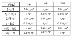
中性点電流重畳部532は、中性点電流指令値算出部531で得た中性点電流指令値i_np*を、各相の循環電流指令値に重畳する。その方法をU相交流電圧の位相θ=π/3~2π/3のときを例に説明する。このとき、U相交流電圧は正、V、W相交流電圧は負である。よって、U相循環電流は正側コンデンサ2aから供給され、V、W相循環電流は負側コンデンサ2bから供給される。
The neutral point current superimposing unit 532 superimposes the neutral point current command value i_np * obtained by the neutral point current command value calculating unit 531 on the circulating current command value of each phase. This method will be described by taking the case where the phase θ of the U-phase AC voltage is θ = π / 3 to 2π / 3 as an example. At this time, the U-phase AC voltage is positive, and the V-phase and W-phase AC voltages are negative. Therefore, the U-phase circulating current is supplied from the positive capacitor 2a, and the V and W-phase circulating currents are supplied from the negative capacitor 2b.
中性点電流指令値i_np*をコンデンサ2a,2bが供給する循環電流に反映させるには、U相循環電流指令値i_c_u0*にi_np*を加算し、V、W相循環電流指令値i_c_v0*、i_c_w0*にはi_np*/2を分配して減算する。これにより、中性点電位を一定にするための各相の循環電流指令値i_c_u1*,i_c_v1*,i_c_w1*を算出する。
In order to reflect the neutral point current command value i_np * in the circulating current supplied by the capacitors 2a and 2b, i_np * is added to the U-phase circulating current command value i_c_u0 *, and the V and W-phase circulating current command values i_c_v0 *, i_np * / 2 is distributed and subtracted from i_c_w0 *. Thus, the circulating current command values i_c_u1 *, i_c_v1 *, i_c_w1 * for each phase for making the neutral point potential constant are calculated.
U相交流電圧の位相θ=π/3~2π/3以外の中性点電流指令値i_np*の重畳方法は同様であり、その重畳量は図4に示した通りである。すなわち、三相のうち、二相が正、一相が負の場合、正の二相においてはi_np*/2ずつ加算し、負の一相においては-i_np*を加算する。一相が正、二相が負の場合、正の一相においてi_np*を加算し、負の二相において-i_np*/2ずつ加算する。なお、三相の中性点電流指令値を合計するとゼロとなる。
The superposition method of the neutral point current command value i_np * other than the phase θ = π / 3 to 2π / 3 of the U-phase AC voltage is the same, and the superposition amount is as shown in FIG. That is, of the three phases, when two phases are positive and one phase is negative, i_np * / 2 is added in the positive two phases, and -i_np * is added in the negative one phase. When one phase is positive and two phases are negative, i_np * is added in one positive phase, and -i_np * / 2 is added in two negative phases. The total of the three-phase neutral point current command values is zero.
なお、二相構成の電力変換装置の場合も、同様の制御方法で中性点電圧を一定にできる。
In the case of a two-phase power converter, the neutral point voltage can be made constant by the same control method.
中性点電位制御部53は、得られた中性点電位を一定にするための各相の循環電流指令値i_c_u1*,i_c_v1*,i_c_w1*をアーム間コンデンサ電圧制御部54に出力する。
The neutral point potential control unit 53 outputs the circulating current command values i_c_u1 *, i_c_v1 *, i_c_w1 * of each phase for making the obtained neutral point potential constant to the inter-arm capacitor voltage control unit 54.
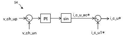
アーム間コンデンサ電圧バランス制御部54は、チョッパセル群回路35のコンデンサ電圧平均値v_ch_up及びチョッパセル群回路36のコンデンサ電圧平均値v_ch_unを同一にする。これを実現するため、出力交流電圧が直流中性点電圧より大きいときは、直流正端子-スイッチ31-チョッパセル群回路35-チョッパセル群回路36-スイッチ33-直流中性点Nの経路に、出力交流電圧と同一周波数の交流循環電流を流す。出力交流電圧が直流中性点電圧より小さいときは、直流中性点N-スイッチ32-チョッパセル群回路35-チョッパセル群回路36-スイッチ34-直流負端子の経路に、出力交流電圧と同一周波数の交流循環電流を流す。
The inter-arm capacitor voltage balance control unit 54 makes the capacitor voltage average value v_ch_up of the chopper cell group circuit 35 and the capacitor voltage average value v_ch_un of the chopper cell group circuit 36 the same. To realize this, when the output AC voltage is larger than the DC neutral point voltage, the output is made to the path of DC positive terminal-switch 31-chopper cell group circuit 35-chopper cell group circuit 36-switch 33-DC neutral point N. An AC circulating current with the same frequency as the AC voltage is applied. When the output AC voltage is smaller than the DC neutral point voltage, the DC neutral point N-switch 32-chopper cell group circuit 35-chopper cell group circuit 36-switch 34-DC negative terminal has the same frequency as the output AC voltage. Apply AC circulating current.
すなわち、図5に示すように、上アーム35のコンデンサ電圧平均値v_ch_up及び下アーム36のコンデンサ電圧平均値v_ch_unの入力を受け、v_ch_upからv_ch_unを減算して比例積分制御した値を正弦関数に代入した値を交流循環電流指令値i_c_ac*とする。これと中性点電位を一定にするためのU相の循環電流指令値i_c_u1*とを加算することで、U相循環電流指令値i_c_u*を算出する。従って、U相循環電流指令値i_c_u*は、直流循環電流に交流循環電流を足し合わせたものとなる。アーム間コンデンサ電圧制御部54は、同様にV相、W相についても循環電流指令値を算出し、算出した各相循環電流指令値i_c_u*,i_c_v*,i_c_w*を循環電流ACR部55に出力する。
That is, as shown in FIG. 5, the capacitor voltage average value v_ch_up of the upper arm 35 and the capacitor voltage average value v_ch_un of the lower arm 36 are received, and the value obtained by subtracting v_ch_un from v_ch_up and substituting the value for proportional integration control is substituted into the sine function. The obtained value is set as an AC circulating current command value i_c_ac *. The U-phase circulating current command value i_c_u * is calculated by adding this and the U-phase circulating current command value i_c_u1 * for making the neutral point potential constant. Therefore, the U-phase circulating current command value i_c_u * is obtained by adding the AC circulating current to the DC circulating current. Similarly, the inter-arm capacitor voltage control unit 54 calculates the circulating current command values for the V phase and the W phase, and outputs the calculated phase circulating current command values i_c_u *, i_c_v *, i_c_w * to the circulating current ACR unit 55. To do.
循環電流ACR部55は、入力されたU相循環電流指令値i_c_u*にU相循環電流i_c_uが追従するように比例積分制御を行い、U相循環電圧指令値v_c_u*を生成する。循環電流ACR55は、同様にV相、W相についても生成し、各相の循環電圧指令値v_c_u*,v_c_v*,v_c_w*をチョッパセル群出力電圧指令値生成部56に出力する。
The circulating current ACR unit 55 performs proportional-integral control so that the U-phase circulating current i_c_u follows the input U-phase circulating current command value i_c_u *, and generates a U-phase circulating voltage command value v_c_u *. Similarly, the circulating current ACR 55 is generated for the V phase and the W phase, and the circulating voltage command values v_c_u *, v_c_v *, and v_c_w * of each phase are output to the chopper cell group output voltage command value generation unit 56.
次いで、チョッパセル群出力電圧指令値生成部56は、各チョッパセル群回路35,36が出力する電圧指令値を生成する。U相を例に図6で説明すると、図6のタイミングt1のように、交流電圧指令値v_u*が直流中性点電圧v_dc_nより大きいときは、スイッチ31,33をオンにし、スイッチ32,34をオフにする。チョッパセル群回路35が入力直流電圧v_dcと出力交流電圧v_ac_uの差電圧を出力し、チョッパセル群回路36が出力交流電圧v_ac_uと直流中性点電圧v_dc_nの差電圧を出力する。図6のタイミングt2のように、交流電圧指令値v_u*が直流中性点電圧v_dc_nより小さいときは、スイッチ32,34をオンにし、スイッチ31,33をオフにする。チョッパセル群回路35が直流中性点電圧v_dc_nと出力交流電圧v_ac_uの差電圧を出力し、チョッパセル群回路36が出力交流電圧v_ac_uと直流負電圧の差電圧を出力する。
Next, the chopper cell group output voltage command value generation unit 56 generates voltage command values output from the chopper cell group circuits 35 and 36. Referring to FIG. 6 by taking the U phase as an example, when the AC voltage command value v_u * is greater than the DC neutral point voltage v_dc_n, as shown at timing t1 in FIG. Turn off. The chopper cell group circuit 35 outputs a difference voltage between the input DC voltage v_dc and the output AC voltage v_ac_u, and the chopper cell group circuit 36 outputs a difference voltage between the output AC voltage v_ac_u and the DC neutral point voltage v_dc_n. When the AC voltage command value v_u * is smaller than the DC neutral point voltage v_dc_n at the timing t2 in FIG. 6, the switches 32 and 34 are turned on and the switches 31 and 33 are turned off. The chopper cell group circuit 35 outputs a difference voltage between the DC neutral point voltage v_dc_n and the output AC voltage v_ac_u, and the chopper cell group circuit 36 outputs a difference voltage between the output AC voltage v_ac_u and the DC negative voltage.
これらの差電圧は、図7に示すチョッパセル群出力電圧指令値生成部56によって実現される。U相上アーム電圧指令値v_up*は、交流電圧指令値v_u*が直流中性点電圧v_dc_n以上のときは、v_up*=v_dc-v_u*-v_c_u*とし、交流電圧指令値v_u*が直流中性点電圧v_dc_nより小さいときは、v_up*=v_dc_n-v_u*-v_c_u*で演算される。U相下アーム電圧指令値v_un*は、交流電圧指令値v_u*が直流中性点電圧v_dc_n以上のときは、v_un*=v_u*-v_dc_n-v_c_u*とし、交流電圧指令値v_u*が直流中性点電圧v_dc_nより小さいときは、v_un*=v_u*-v_c_u*で演算される。
These differential voltages are realized by the chopper cell group output voltage command value generation unit 56 shown in FIG. The U-phase upper arm voltage command value v_up * is v_up * = v_dc−v_u * −v_c_u * when the AC voltage command value v_u * is equal to or higher than the DC neutral point voltage v_dc_n, and the AC voltage command value v_u * is in the DC state. When it is smaller than the sex point voltage v_dc_n, it is calculated by v_up * = v_dc_n−v_u * −v_c_u *. The U-phase lower arm voltage command value v_un * is v_un * = v_u * −v_dc_n−v_c_u * when the AC voltage command value v_u * is equal to or greater than the DC neutral point voltage v_dc_n, and the AC voltage command value v_u * is in the DC state. When it is smaller than the sex point voltage v_dc_n, it is calculated by v_un * = v_u * −v_c_u *.
個別コンデンサ電圧バランス制御部57は、チョッパセル群回路35,36の各チョッパセルCの出力電圧を同一になるように調整する。すなわち、U相上アーム電流i_upが正のときコンデンサは充電されるので、コンデンサ電圧が小さいチョッパセルCの出力電圧を大きくし、コンデンサ電圧が大きいチョッパセルCの出力電圧は小さくする。U相上アーム電流i_upが負のときコンデンサは放電されるので、コンデンサ電圧が小さいチョッパセルCの出力電圧を小さくし、コンデンサ電圧が大きいチョッパセルCの出力電圧は大きくする。
The individual capacitor voltage balance control unit 57 adjusts the output voltages of the chopper cells C of the chopper cell group circuits 35 and 36 to be the same. That is, since the capacitor is charged when the U-phase upper arm current i_up is positive, the output voltage of the chopper cell C having a small capacitor voltage is increased, and the output voltage of the chopper cell C having a large capacitor voltage is decreased. Since the capacitor is discharged when the U-phase upper arm current i_up is negative, the output voltage of the chopper cell C having a small capacitor voltage is decreased, and the output voltage of the chopper cell C having a large capacitor voltage is increased.
このような制御動作を実現するために、個別コンデンサ電圧バランス制御部57は、U相のチョッパセル群回路35を例に説明すると、図8に示すように、コンデンサ電圧v_ch_up1からチョッパセル群回路35のコンデンサ電圧平均値v_ch_upを減算し、これに比例ゲインを乗算した値に、U相アーム電流i_upの符号を反転させた値-sign(i_up)を乗算し、U相アーム電圧指令値v_up*を加算し、各チョッパセルの電圧指令値v_up1*,v_up2*,v_up3*を算出する。
In order to realize such a control operation, the individual capacitor voltage balance control unit 57 will be described by taking the U-phase chopper cell group circuit 35 as an example. As shown in FIG. 8, the capacitor voltage of the chopper cell group circuit 35 is obtained from the capacitor voltage v_ch_up1. The value obtained by subtracting the voltage average value v_ch_up and multiplying this by the proportional gain is multiplied by a value −sign (i_up) obtained by inverting the sign of the U-phase arm current i_up, and the U-phase arm voltage command value v_up * is added. The voltage command values v_up1 *, v_up2 *, and v_up3 * of each chopper cell are calculated.
次に、チョッパセルCの電圧出力方法を説明する。この方法は全チョッパセルCで同じであるため、チョッパセルch_up1を例に、図9を用いて説明する。なお、チョッパセルch_up1を構成する2個のスイッチをsw_ch_up11,sw_ch_up12とする。
Next, the voltage output method of the chopper cell C will be described. Since this method is the same for all chopper cells C, a chopper cell ch_up1 will be described as an example with reference to FIG. Note that the two switches constituting the chopper cell ch_up1 are sw_ch_up11 and sw_ch_up12.
チョッパセルch_up1の出力電圧指令値v_up1*を出力するため、キャリア三角波car_up1と比較し、出力電圧指令値v_up1*がキャリア三角波car_up1より大きいときは、スイッチsw_ch_up11をオンにし、sw_ch_up12をオフにする。出力電圧指令値v_up1*がキャリア三角波car_up1より小さいときは、スイッチsw_ch_up11をオフにし、sw_ch_up12をオンにする。
In order to output the output voltage command value v_up1 * of the chopper cell ch_up1, it is compared with the carrier triangular wave car_up1, and when the output voltage command value v_up1 * is larger than the carrier triangular wave car_up1, the switch sw_ch_up11 is turned on and the sw_ch_up12 is turned off. When the output voltage command value v_up1 * is smaller than the carrier triangular wave car_up1, the switch sw_ch_up11 is turned off and the sw_ch_up12 is turned on.
チョッパセル群回路35がN個のチョッパセルCで構成される場合、キャリア三角波の位相を360°/Nずつずらすことにより、等価キャリア周波数をキャリア三角波周波数のN倍に大きくでき、各スイッチのオンオフをより細かく行う。従って、出力交流電圧の高調波電圧を低減し出力交流電圧を滑らかにすることができる。また、チョッパセル群回路36に用いるキャリア三角波位相を、チョッパセル群回路35と同一にすることにより、更に出力交流電圧の高調波電圧を低減することができる。
When the chopper cell group circuit 35 is composed of N chopper cells C, the equivalent carrier frequency can be increased to N times the carrier triangular wave frequency by shifting the phase of the carrier triangular wave by 360 ° / N, and each switch can be turned on and off more. Do it finely. Therefore, the harmonic voltage of the output AC voltage can be reduced and the output AC voltage can be made smooth. Further, by making the carrier triangular wave phase used for the chopper cell group circuit 36 the same as that of the chopper cell group circuit 35, the harmonic voltage of the output AC voltage can be further reduced.
[1-3.作用・効果]
(1)本実施形態の電力変換装置1は、交流と直流の間で電力を変換する電力変換装置であって、直流電源20と並列に接続され、直流電源20の入力直流電圧を分割して中性点電位を作るための直列接続されたコンデンサ2a,2bと、直流電源20と並列に各々接続され、直流を交流に変換するためのチョッパセルCを含む複数のレグ3と、各相のレグ3のチョッパセル出力電圧をバランスさせるために各相のレグ3内に流す循環電流を制御する制御部5と、を備え、制御部5は、各相の直流端子間に流す直流循環電流に、中性点電位を一定に制御するための中性点電流を重畳する中性点電位制御部53を有し、中性点電位制御部53は、コンデンサ2a,2bの少なくとも何れかに中性点電流を重畳した循環電流を流させるようにした。 [1-3. Action / Effect]
(1) Thepower conversion device 1 of the present embodiment is a power conversion device that converts power between alternating current and direct current, and is connected in parallel with the direct current power source 20 to divide the input direct current voltage of the direct current power source 20. Capacitors 2a and 2b connected in series for generating a neutral point potential, a plurality of legs 3 each connected in parallel with a DC power supply 20 and including a chopper cell C for converting DC to AC, and a leg for each phase 3 to control the circulating current that flows in the leg 3 of each phase in order to balance the output voltage of the three chopper cells, and the control unit 5 A neutral point potential control unit 53 for superimposing a neutral point current for controlling the neutral point potential to be constant is provided, and the neutral point potential control unit 53 is connected to at least one of the capacitors 2a and 2b. Circulated current superimposed on
(1)本実施形態の電力変換装置1は、交流と直流の間で電力を変換する電力変換装置であって、直流電源20と並列に接続され、直流電源20の入力直流電圧を分割して中性点電位を作るための直列接続されたコンデンサ2a,2bと、直流電源20と並列に各々接続され、直流を交流に変換するためのチョッパセルCを含む複数のレグ3と、各相のレグ3のチョッパセル出力電圧をバランスさせるために各相のレグ3内に流す循環電流を制御する制御部5と、を備え、制御部5は、各相の直流端子間に流す直流循環電流に、中性点電位を一定に制御するための中性点電流を重畳する中性点電位制御部53を有し、中性点電位制御部53は、コンデンサ2a,2bの少なくとも何れかに中性点電流を重畳した循環電流を流させるようにした。 [1-3. Action / Effect]
(1) The
これにより、中性点電位を一定に保つことのできる中性点クランプ形の電力変換装置を得ることができる。また、中性点電位を一定に保つためには零相電圧を印加する方法も考えられるが、この場合、出力交流電圧の周波数に制御応答速度が依存し、結果的に中性点電位変動が大きくなり、直流コンデンサ容量を大きくなる虞がある。これに対し、本実施形態によれば、中性点電流を一周期のうちいつでも流すことができるので、出力交流電圧の周波数に依存しない制御応答速度を実現できる。
This makes it possible to obtain a neutral point clamp type power converter that can keep the neutral point potential constant. In order to keep the neutral point potential constant, a method of applying a zero-phase voltage is also conceivable, but in this case, the control response speed depends on the frequency of the output AC voltage, resulting in neutral point potential fluctuations. There is a risk of increasing the DC capacitor capacity. On the other hand, according to the present embodiment, the neutral point current can be flowed at any time during one period, so that a control response speed independent of the frequency of the output AC voltage can be realized.
また、レグ3は、多直列接続されたスイッチ31~34と、チョッパセルCが1つ又は2つ以上直列接続された一対のチョッパセル群回路35,36と、を有し、スイッチ31~34は、この順で直流電源20と接続される直流正端子から直流負端子の間に設け、スイッチ32及びスイッチ33の間で直流中性点Nと接続され、一対のチョッパセル群回路35,36は、スイッチ32,33と並列に接続するようにした。これにより、従来のMMCと比較してチョッパセル数を半数に減らすことができ、電力変換装置サイズを小さくすることができる。加えて、直流コンデンサ容量はチョッパセルのコンデンサ容量より小さく、電力変換装置サイズを小さくできる。また、チョッパセル数低減によりスイッチング損失が低減して変換効率を向上させることができる。
The leg 3 includes multiple switches 31 to 34 connected in series and a pair of chopper cell group circuits 35 and 36 in which one or more chopper cells C are connected in series. In this order, it is provided between a DC positive terminal and a DC negative terminal connected to the DC power supply 20, and is connected to the DC neutral point N between the switch 32 and the switch 33. 32 and 33 are connected in parallel. Thereby, compared with the conventional MMC, the number of chopper cells can be reduced to half, and the size of the power converter can be reduced. In addition, the DC capacitor capacity is smaller than that of the chopper cell, and the size of the power converter can be reduced. Moreover, switching loss can be reduced and conversion efficiency can be improved by reducing the number of chopper cells.
(2)中性点電位制御部53は、コンデンサ2a,2bのうち、高電圧なコンデンサから放電させた電力を低電圧なコンデンサに充電させるようにした。これにより、中性点電位を一定に制御しやすくできる。例えば、正側コンデンサ2aが高電圧で、負側コンデンサ2bが低電圧の場合、正側コンデンサ2aの放電電流が、他の二相のレグ3を介して負側コンデンサ2bに充電され、コンデンサ2a,2bのバランスを取るため、双方のコンデンサ2a,2bを制御した方が中性点電位を一定に保たせやすくなる。
(2) The neutral point potential control unit 53 charges the low-voltage capacitor with the power discharged from the high-voltage capacitor among the capacitors 2a and 2b. Thereby, it is possible to easily control the neutral point potential to be constant. For example, when the positive side capacitor 2a has a high voltage and the negative side capacitor 2b has a low voltage, the discharge current of the positive side capacitor 2a is charged to the negative side capacitor 2b via the other two-phase leg 3, and the capacitor 2a , 2b, it is easier to keep the neutral point potential constant by controlling both capacitors 2a, 2b.
(3)中性点電位制御部53は、中性点電流を各相のレグ3に分配して重畳するようにした。これにより、重畳される中性点電流が各相のレグ3に分散されるので、スイッチ31~34に流れる電流増大に伴う熱的負担等の負担を低減することができる。分配して重畳させない方法としては、例えば、U相レグ3にのみ中性点電流を流し、正側コンデンサ2aを放電させてチョッパセル群回路35のコンデンサに充電させ、V相、W相レグ3には流さないように制御することも可能であるが、この場合、U相にのみ中性点電流を重畳させるので、U相レグ3のスイッチ31~34に熱的な負担が増大する。これに対し、本実施形態の方法によれば、その負担を各相レグ3に分散することができる。
(3) The neutral point potential control unit 53 distributes and superimposes the neutral point current to the leg 3 of each phase. As a result, the neutral point current to be superimposed is distributed to the leg 3 of each phase, so that it is possible to reduce a burden such as a thermal burden accompanying an increase in the current flowing through the switches 31 to 34. As a method of distributing and not superimposing, for example, a neutral point current is allowed to flow only in the U-phase leg 3, the positive capacitor 2 a is discharged and charged in the capacitor of the chopper cell group circuit 35, and the V-phase and W-phase leg 3 is charged. However, in this case, since the neutral point current is superimposed only on the U phase, the thermal load on the switches 31 to 34 of the U phase leg 3 increases. On the other hand, according to the method of the present embodiment, the burden can be distributed to each phase leg 3.
(4)中性点電位制御部53は、中性点電流の指令値i_np*を、コンデンサ2a,2bの電圧差を比例積分制御することにより算出するようにした。これにより、コンデンサ2a,2bの電圧が同じになり、中性点電位を一定に制御することができる。
(4) The neutral point potential control unit 53 calculates the neutral point current command value i_np * by proportional-integral control of the voltage difference between the capacitors 2a and 2b. Thereby, the voltages of the capacitors 2a and 2b become the same, and the neutral point potential can be controlled to be constant.
(5)中性点電位制御部53は、コンデンサ2a,2bの電圧差に含まれる高周波数成分を除去するローパスフィルタを有するようにした。これにより、安定した中性点電流指令値を生成することができるので、高周波成分を有することによる制御への影響を排除することができる。
(5) The neutral point potential control unit 53 includes a low-pass filter that removes a high-frequency component included in the voltage difference between the capacitors 2a and 2b. As a result, a stable neutral point current command value can be generated, so that it is possible to eliminate the influence on control due to having a high-frequency component.
(6)中性点電位制御部53は、コンデンサ2a,2bの電圧差に含まれる高周波数成分を除去する移動平均フィルタを有するようにした。これにより、安定した中性点電流指令値を生成することができるので、高周波成分を有することによる制御への影響を排除することができる。
(6) The neutral point potential control unit 53 has a moving average filter that removes high frequency components included in the voltage difference between the capacitors 2a and 2b. As a result, a stable neutral point current command value can be generated, so that it is possible to eliminate the influence on control due to having a high-frequency component.
(7)移動平均フィルタの移動平均周期を、出力交流電圧周期のレグ数倍以上とした。これにより、中性点電流指令値を算出するためのコンデンサ2a,2bの電圧差から、出力交流電圧周期のレグ数倍の高調波成分を除去することができるので、効率的に制御への影響を排除することができる。
(7) The moving average period of the moving average filter is set to be not less than the number of legs of the output AC voltage period. As a result, the harmonic component of the output AC voltage cycle times the number of legs can be removed from the voltage difference between the capacitors 2a and 2b for calculating the neutral point current command value, thereby effectively affecting the control. Can be eliminated.
[2.その他の実施形態]
本明細書においては、本発明に係る複数の実施形態を説明したが、これらの実施形態は例として提示したものであって、発明の範囲を限定することを意図していない。以上のような実施形態は、その他の様々な形態で実施されることが可能であり、発明の範囲を逸脱しない範囲で、種々の省略や置き換え、変更を行うことができる。これらの実施形態やその変形は、発明の範囲や要旨に含まれると同様に、請求の範囲に記載された発明とその均等の範囲に含まれるものである。 [2. Other Embodiments]
In the present specification, a plurality of embodiments according to the present invention have been described. However, these embodiments are presented as examples and are not intended to limit the scope of the invention. The above embodiments can be implemented in other various forms, and various omissions, replacements, and changes can be made without departing from the scope of the invention. These embodiments and modifications thereof are included in the invention described in the claims and equivalents thereof, as long as they are included in the scope and gist of the invention.
例えば、第1の実施形態では、2つのコンデンサ2a,2bにより中性点電位を形成したが、正側で多直列接続したコンデンサと、負側で多直列接続したコンデンサとで中性点電位を形成するようにしても良い。これにより、耐電圧を大きくすることができる。また、コンデンサ2a,2bのそれぞれに対し、2個以上のコンデンサを並列接続してコンデンサ容量を大きくするようにしても良い。
For example, in the first embodiment, the neutral point potential is formed by the two capacitors 2a and 2b. However, the neutral point potential is determined by a capacitor connected in series on the positive side and a capacitor connected in series on the negative side. You may make it form. Thereby, a withstand voltage can be enlarged. Further, two or more capacitors may be connected in parallel to each of the capacitors 2a and 2b to increase the capacitor capacity.
更に、第1の実施形態では、直列接続された2つのコンデンサ2a,2bに対し、3相のレグ3をそれぞれ並列接続したが、各相のレグ3に対し、直列接続された2つのコンデンサ2a,2bをそれぞれ直近に並列接続するようにしても良い。これにより、スイッチ31~34をオフにするときに、各相のレグ間に寄生のインダクタンスが残ることによるサージ電圧の印加を防止することができる。
Further, in the first embodiment, the three-phase legs 3 are connected in parallel to the two capacitors 2a and 2b connected in series. However, the two capacitors 2a connected in series to the leg 3 in each phase are connected. , 2b may be connected in parallel most recently. As a result, when the switches 31 to 34 are turned off, it is possible to prevent application of surge voltage due to parasitic inductance remaining between the legs of each phase.
1 電力変換装置
2a,2b コンデンサ
20 直流電源
21 三相トランスtr
22 電力系統V_S
3 レグ
31~34 スイッチ
35 チョッパセル群回路(上アーム)
36 チョッパセル群回路(下アーム)
37,38 リアクトル
39 出力交流電圧端子
5 制御部
51 各相出力電圧制御部
511 3相/DQ変換部
512 ACR部
513 DQ/3相変換部
52 各相コンデンサ電圧バランス制御部
53 中性点電位制御部
531 中性点電流指令値算出部
532 中性点電流重畳部
54 アーム間コンデンサ電圧バランス制御部
55 循環電流ACR部
56 チョッパセル群出力電圧指令値生成部
57 個別コンデンサ電圧バランス制御部
C チョッパセル
N 直流中性点
sw_ch1,sw_ch2 チョッパセルのスイッチ
101 MMC
103 レグ
104a 上アーム
104b 下アーム
105 レグ
120 直流電源
121 三相トランス
122 電力系統
139 交流出力端子 DESCRIPTION OFSYMBOLS 1 Power converter device 2a, 2b Capacitor 20 DC power supply 21 Three-phase transformer tr
22 Power system V_S
3Leg 31 to 34 Switch 35 Chopper cell group circuit (upper arm)
36 Chopper cell group circuit (lower arm)
37, 38Reactor 39 Output AC voltage terminal 5 Control section 51 Each phase output voltage control section 511 Three phase / DQ conversion section 512 ACR section 513 DQ / 3 phase conversion section 52 Each phase capacitor voltage balance control section 53 Neutral point potential control Unit 531 neutral point current command value calculation unit 532 neutral point current superimposition unit 54 arm-to-arm capacitor voltage balance control unit 55 circulating current ACR unit 56 chopper cell group output voltage command value generation unit 57 individual capacitor voltage balance control unit C chopper cell N DC Neutral point sw_ch1, sw_ch2 Chopper cell switch 101 MMC
103leg 104a upper arm 104b lower arm 105 leg 120 DC power supply 121 three-phase transformer 122 power system 139 AC output terminal
2a,2b コンデンサ
20 直流電源
21 三相トランスtr
22 電力系統V_S
3 レグ
31~34 スイッチ
35 チョッパセル群回路(上アーム)
36 チョッパセル群回路(下アーム)
37,38 リアクトル
39 出力交流電圧端子
5 制御部
51 各相出力電圧制御部
511 3相/DQ変換部
512 ACR部
513 DQ/3相変換部
52 各相コンデンサ電圧バランス制御部
53 中性点電位制御部
531 中性点電流指令値算出部
532 中性点電流重畳部
54 アーム間コンデンサ電圧バランス制御部
55 循環電流ACR部
56 チョッパセル群出力電圧指令値生成部
57 個別コンデンサ電圧バランス制御部
C チョッパセル
N 直流中性点
sw_ch1,sw_ch2 チョッパセルのスイッチ
101 MMC
103 レグ
104a 上アーム
104b 下アーム
105 レグ
120 直流電源
121 三相トランス
122 電力系統
139 交流出力端子 DESCRIPTION OF
22 Power system V_S
3
36 Chopper cell group circuit (lower arm)
37, 38
103
Claims (8)
- 交流と直流の間で電力を変換する電力変換装置であって、
直流電源と並列に接続され、前記直流電源の入力直流電圧を分割して中性点電位を作るための直列接続された第1及び第2のコンデンサと、
前記直流電源と並列に各々接続され、直流を交流に変換するためのチョッパセルを含む複数のレグと、
各相のレグの前記チョッパセル出力電圧をバランスさせるために各相のレグ内に流す循環電流を制御する制御部と、
を備え、
前記制御部は、各相の直流端子間に流す直流循環電流に、中性点電位を一定に制御するための中性点電流を重畳する中性点電位制御部を有し、
前記中性点電位制御部は、前記第1及び第2のコンデンサの少なくとも何れかに前記中性点電流を重畳した循環電流を流させること、
を特徴とする電力変換装置。 A power conversion device that converts power between alternating current and direct current,
First and second capacitors connected in series with a DC power source and connected in series to create a neutral point potential by dividing an input DC voltage of the DC power source;
A plurality of legs each connected in parallel with the direct current power source and including a chopper cell for converting direct current to alternating current;
A controller for controlling the circulating current flowing in each phase leg to balance the chopper cell output voltage of each phase leg;
With
The control unit includes a neutral point potential control unit that superimposes a neutral point current for controlling the neutral point potential to be constant in a DC circulating current flowing between the DC terminals of each phase,
The neutral point potential controller causes a circulating current in which the neutral point current is superimposed on at least one of the first and second capacitors;
The power converter characterized by this. - 前記中性点電位制御部は、前記第1及び第2のコンデンサのうち、高電圧なコンデンサから放電させた電力を低電圧なコンデンサに充電させること、
を特徴とする請求項1記載の電力変換装置。 The neutral point potential controller is configured to charge a low voltage capacitor with power discharged from a high voltage capacitor among the first and second capacitors,
The power conversion device according to claim 1. - 前記中性点電位制御部は、前記中性点電流を各相のレグに分配して重畳すること、
を特徴とする請求項1又は2に記載の電力変換装置。 The neutral point potential control unit distributes and superimposes the neutral point current on the legs of each phase;
The power conversion device according to claim 1, wherein: - 前記中性点電位制御部は、前記中性点電流の指令値を、前記第1及び第2のコンデンサの電圧差を比例積分制御することにより算出すること、
を特徴とする請求項1~3の何れかに記載の電力変換装置。 The neutral point potential control unit calculates a command value of the neutral point current by proportional-integral control of a voltage difference between the first and second capacitors;
The power conversion device according to any one of claims 1 to 3, wherein: - 前記中性点電位制御部は、前記第1及び第2のコンデンサの電圧差に含まれる高周波数成分を除去するローパスフィルタを有すること、
を特徴とする請求項1~4の何れかに記載の電力変換装置。 The neutral point potential control unit includes a low-pass filter that removes a high-frequency component included in a voltage difference between the first and second capacitors;
The power conversion device according to any one of claims 1 to 4, wherein: - 前記中性点電位制御部は、前記第1及び第2のコンデンサの電圧差に含まれる高周波数成分を除去する移動平均フィルタを有すること、
を特徴とする請求項1~4の何れかに記載の電力変換装置。 The neutral point potential control unit includes a moving average filter that removes a high-frequency component included in a voltage difference between the first and second capacitors;
The power conversion device according to any one of claims 1 to 4, wherein: - 前記移動平均フィルタの移動平均周期を、出力交流電圧周期の前記レグ数倍以上とすること、
を特徴とする請求項6に記載の電力変換装置。 The moving average period of the moving average filter is not less than the number of legs of the output AC voltage period;
The power converter according to claim 6 characterized by things. - 前記レグは、
多直列接続された第1乃至第4のスイッチと、
前記チョッパセルが1つ又は2つ以上直列接続された一対のチョッパセル群回路と、
を有し、
前記第1乃至第4のスイッチは、この順で前記直流電源と接続される直流正端子から直流負端子の間に設けられ、前記第2のスイッチ及び前記第3のスイッチの間で中性点と接続され、
前記一対のチョッパセル群回路は、前記第2及び第3のスイッチと並列に接続されていること、
を特徴とする請求項1~7の何れかに記載の電力変換装置。 The leg
First to fourth switches connected in series;
A pair of chopper cells in which one or more chopper cells are connected in series;
Have
The first to fourth switches are provided between a DC positive terminal and a DC negative terminal connected to the DC power source in this order, and a neutral point between the second switch and the third switch. Connected with
The pair of chopper cell group circuits are connected in parallel with the second and third switches;
The power conversion device according to any one of claims 1 to 7, wherein:
Priority Applications (2)
| Application Number | Priority Date | Filing Date | Title |
|---|---|---|---|
| EP15836708.6A EP3188356A4 (en) | 2014-08-25 | 2015-07-21 | Power conversion device |
| CN201580045581.3A CN106575929B (en) | 2014-08-25 | 2015-07-21 | Power conversion device |
Applications Claiming Priority (2)
| Application Number | Priority Date | Filing Date | Title |
|---|---|---|---|
| JP2014170804A JP6253548B2 (en) | 2014-08-25 | 2014-08-25 | Power converter |
| JP2014-170804 | 2014-08-25 |
Publications (1)
| Publication Number | Publication Date |
|---|---|
| WO2016031430A1 true WO2016031430A1 (en) | 2016-03-03 |
Family
ID=55399331
Family Applications (1)
| Application Number | Title | Priority Date | Filing Date |
|---|---|---|---|
| PCT/JP2015/070665 WO2016031430A1 (en) | 2014-08-25 | 2015-07-21 | Power conversion device |
Country Status (4)
| Country | Link |
|---|---|
| EP (1) | EP3188356A4 (en) |
| JP (1) | JP6253548B2 (en) |
| CN (1) | CN106575929B (en) |
| WO (1) | WO2016031430A1 (en) |
Cited By (2)
| Publication number | Priority date | Publication date | Assignee | Title |
|---|---|---|---|---|
| EP3432461A4 (en) * | 2016-03-15 | 2019-11-13 | Kabushiki Kaisha Toshiba | Power conversion device |
| CN113759181A (en) * | 2020-06-01 | 2021-12-07 | 台达电子工业股份有限公司 | Detection device for voltage unbalance of direct current link capacitor |
Families Citing this family (3)
| Publication number | Priority date | Publication date | Assignee | Title |
|---|---|---|---|---|
| JP6502870B2 (en) * | 2016-02-04 | 2019-04-17 | 株式会社東芝 | Power converter |
| JP6957196B2 (en) * | 2017-05-17 | 2021-11-02 | 株式会社東芝 | Power converter |
| JP6783419B1 (en) * | 2020-03-30 | 2020-11-11 | 三菱電機株式会社 | Power converter |
Citations (3)
| Publication number | Priority date | Publication date | Assignee | Title |
|---|---|---|---|---|
| JP2013099054A (en) * | 2011-10-31 | 2013-05-20 | Hitachi Ltd | Power conversion device |
| JP2013143836A (en) * | 2012-01-11 | 2013-07-22 | Toshiba Mitsubishi-Electric Industrial System Corp | Three-level power conversion device |
| JP2014096969A (en) * | 2012-11-12 | 2014-05-22 | Hitachi Ltd | Power conversion apparatus and power conversion method |
Family Cites Families (4)
| Publication number | Priority date | Publication date | Assignee | Title |
|---|---|---|---|---|
| US8228695B2 (en) * | 2009-11-16 | 2012-07-24 | General Electric Company | Multilevel converter operation |
| US9559611B2 (en) * | 2012-09-28 | 2017-01-31 | General Electric Company | Multilevel power converter system and method |
| US9479075B2 (en) * | 2013-07-31 | 2016-10-25 | General Electric Company | Multilevel converter system |
| JP6219188B2 (en) * | 2014-02-03 | 2017-10-25 | 株式会社東芝 | Power converter |
-
2014
- 2014-08-25 JP JP2014170804A patent/JP6253548B2/en active Active
-
2015
- 2015-07-21 WO PCT/JP2015/070665 patent/WO2016031430A1/en active Application Filing
- 2015-07-21 CN CN201580045581.3A patent/CN106575929B/en active Active
- 2015-07-21 EP EP15836708.6A patent/EP3188356A4/en not_active Withdrawn
Patent Citations (3)
| Publication number | Priority date | Publication date | Assignee | Title |
|---|---|---|---|---|
| JP2013099054A (en) * | 2011-10-31 | 2013-05-20 | Hitachi Ltd | Power conversion device |
| JP2013143836A (en) * | 2012-01-11 | 2013-07-22 | Toshiba Mitsubishi-Electric Industrial System Corp | Three-level power conversion device |
| JP2014096969A (en) * | 2012-11-12 | 2014-05-22 | Hitachi Ltd | Power conversion apparatus and power conversion method |
Non-Patent Citations (1)
| Title |
|---|
| See also references of EP3188356A4 * |
Cited By (2)
| Publication number | Priority date | Publication date | Assignee | Title |
|---|---|---|---|---|
| EP3432461A4 (en) * | 2016-03-15 | 2019-11-13 | Kabushiki Kaisha Toshiba | Power conversion device |
| CN113759181A (en) * | 2020-06-01 | 2021-12-07 | 台达电子工业股份有限公司 | Detection device for voltage unbalance of direct current link capacitor |
Also Published As
| Publication number | Publication date |
|---|---|
| JP6253548B2 (en) | 2017-12-27 |
| EP3188356A1 (en) | 2017-07-05 |
| CN106575929B (en) | 2019-09-24 |
| CN106575929A (en) | 2017-04-19 |
| EP3188356A4 (en) | 2018-04-25 |
| JP2016046955A (en) | 2016-04-04 |
Similar Documents
| Publication | Publication Date | Title |
|---|---|---|
| US10727762B2 (en) | Modular, multi-channel, interleaved power converters | |
| EP2491644B1 (en) | System and method for offsetting the input voltage unbalance in multilevel inverters or the like | |
| US9960709B2 (en) | Power conversion device | |
| JP6219188B2 (en) | Power converter | |
| JP6416436B2 (en) | Power converter | |
| WO2016031430A1 (en) | Power conversion device | |
| JP2014509824A (en) | Grid-connected inverter, inverter device, and method for operating the inverter device | |
| WO2017046910A1 (en) | Power conversion device | |
| US9755551B2 (en) | Power conversion device | |
| JP6494378B2 (en) | Power conversion system and method for controlling power conversion system | |
| JP2018196237A (en) | Power conversion device | |
| JP2018129963A (en) | Controller of power converter | |
| JP6524000B2 (en) | Power converter | |
| US20200228028A1 (en) | Inverter system | |
| JP6502870B2 (en) | Power converter | |
| Behrouzian et al. | Individual capacitor voltage balancing in H-bridge cascaded multilevel STATCOM at zero current operating mode | |
| Wang et al. | Parallel interlinking PWM current source converter for hybrid AC/DC microgrids | |
| JP2012080753A (en) | Power conversion equipment | |
| Itoh et al. | Experimental verification of a multi-level inverter with H-bridge clamp circuit for single-phase three-wire grid connection | |
| BHAGAVATHI et al. | Bridgeless Multi Level Inverter for Single Phase and Three Phase Applications | |
| Plyusnin | Multilevel modular converters for off-shore wind farm HVDC transmission system | |
| Liu et al. | A direct power conversion topology for grid integrations of hybrid AC/DC resources |
Legal Events
| Date | Code | Title | Description |
|---|---|---|---|
| 121 | Ep: the epo has been informed by wipo that ep was designated in this application |
Ref document number: 15836708 Country of ref document: EP Kind code of ref document: A1 |
|
| NENP | Non-entry into the national phase |
Ref country code: DE |
|
| REEP | Request for entry into the european phase |
Ref document number: 2015836708 Country of ref document: EP |
|
| WWE | Wipo information: entry into national phase |
Ref document number: 2015836708 Country of ref document: EP |