JP6515836B2 - Inverter device - Google Patents
Inverter device Download PDFInfo
- Publication number
- JP6515836B2 JP6515836B2 JP2016032908A JP2016032908A JP6515836B2 JP 6515836 B2 JP6515836 B2 JP 6515836B2 JP 2016032908 A JP2016032908 A JP 2016032908A JP 2016032908 A JP2016032908 A JP 2016032908A JP 6515836 B2 JP6515836 B2 JP 6515836B2
- Authority
- JP
- Japan
- Prior art keywords
- power module
- substrate
- power
- terminal
- orthogonal direction
- Prior art date
- Legal status (The legal status is an assumption and is not a legal conclusion. Google has not performed a legal analysis and makes no representation as to the accuracy of the status listed.)
- Active
Links
Images


Description
本発明は、直流電力と複数相の交流電力との間で電力を変換するインバータ回路を備えたインバータ装置に関する。 The present invention relates to an inverter device provided with an inverter circuit that converts power between DC power and AC power of multiple phases.
特開2006−81311号公報(特許文献1)には、直流電力と複数相の交流電力との間で電力を変換するインバータ回路を備えたインバータ装置としてのパワードライブユニット(22)が開示されている(括弧内の符号は特許文献1のもの。背景技術の説明において以下同様。)。このパワードライブユニット(22)は、制御回路基板(40)、パワーモジュール(42)、ヒートシンク(48)、電流センサ(26)を備えている。特許文献1の図2、図7等に示されているように、制御回路基板(40)、パワーモジュール(42)、ヒートシンク(48)は、制御回路基板(40)に直交する方向(基板直交方向)に順に重ねて配置されている。パワーモジュール(42)からは、制御回路基板(40)の面に沿う方向に3相交流電流が流れるバスバー(44)が、突出するように設けられている。バスバー(44)の先端部は、モータ(20)との電気的接続部材に接続するために、基板直交方向に見て制御回路基板(44)からはみ出す位置に配置されており、接続孔(44a)が設けられている。
Japanese Patent Laid-Open No. 2006-81311 (Patent Document 1) discloses a power drive unit (22) as an inverter device provided with an inverter circuit for converting power between DC power and AC power of a plurality of phases. (The reference numerals in parentheses are those of
ところで、このようなパワーモジュールは、電力型半導体スイッチング素子(パワースイッチング素子)を有して構成されている。近年、パワースイッチング素子に利用できる半導体材料の進歩や、素子形成技術の進歩に伴う電気的特性の向上(耐圧性能や最大電流の向上など)により、パワーモジュールの小型化が進んでいる。そのため、パワーモジュールの制御回路を備えた制御基板の平面視での大きさがパワーモジュールに比べて大きい場合が生じる。そのような場合において、パワーモジュールから伸びる交流バスバーや、当該交流バスバーの周辺に設けられる電流センサ等を適切に配置しなければ、パワーモジュールに隣接すると共に平面視で制御基板と重複する領域に余剰空間が生じる場合がある。 By the way, such a power module is configured to have a power type semiconductor switching element (power switching element). 2. Description of the Related Art In recent years, miniaturization of power modules has progressed due to advances in semiconductor materials that can be used for power switching elements, and improvements in electrical characteristics (such as improvements in withstand voltage performance and maximum current) accompanying advances in element formation technology. Therefore, the size in a plan view of the control substrate provided with the control circuit of the power module may be larger than that of the power module. In such a case, unless the AC bus bar extending from the power module, the current sensor and the like provided around the AC bus bar, etc. are properly arranged, the surplus in the area adjacent to the power module and overlapping the control substrate in plan view Space may occur.
上記背景に鑑みて、制御基板、パワーモジュール、バスバーなどインバータ装置を構成する部材を効率的に配置して、インバータ装置の全体を小型化できる構成の実現が望まれる。 In view of the above-mentioned background, realization of the composition which can miniaturize the whole inverter device is desired by arranging efficiently members which constitute an inverter device, such as a control board, a power module, and a bus bar.
上記に鑑みた、直流電力と複数相の交流電力との間で電力を変換するインバータ回路を備えたインバータ装置は、1つの態様として、
前記インバータ回路を構成するスイッチング素子を備えたパワーモジュールと、
前記パワーモジュールに接して前記パワーモジュールを冷却する冷却モジュールと、
前記スイッチング素子をスイッチング制御する制御回路を備えた制御基板と、
前記パワーモジュールの交流電力の入出力端子である交流端子に接続される交流バスバーと、
前記交流バスバーを流れる複数相の交流電流を検出する電流センサと、
を備え、
前記制御基板と、前記パワーモジュールと、前記冷却モジュールとは、前記制御基板に直交する方向である基板直交方向に見て、少なくとも一部が重複する状態で、前記制御基板、前記パワーモジュール、前記冷却モジュールの順に重ねて配置され、
前記制御基板は、前記基板直交方向に見て、前記パワーモジュールと重複する第1領域と、重複しない第2領域とを有し、
前記交流端子は、前記基板直交方向に見て、前記制御基板と重複しない位置に配置され、
前記電流センサは、前記基板直交方向において前記制御基板よりも前記パワーモジュールの側であって、前記基板直交方向に見て前記第2領域に重複する位置に配置され、
前記冷却モジュールは、前記パワーモジュールを載置する面である第1面と、前記第1面とは反対側の面である第2面とを有し、
前記交流バスバーは、前記交流端子から前記電流センサまでの間の一部の領域において、前記第2面に接するように配置されると共に、前記冷却モジュールに固定されている。
The inverter apparatus provided with the inverter circuit which converts electric power between direct-current power and alternating current power of multiple phases in view of the above as one mode,
A power module provided with a switching element forming the inverter circuit;
A cooling module for cooling the power module in contact with the power module;
A control substrate provided with a control circuit that performs switching control of the switching element;
An AC bus bar connected to an AC terminal which is an input / output terminal of AC power of the power module;
A current sensor for detecting a plurality of phases of alternating current flowing through the alternating current bus bar;
Equipped with
The control substrate, the power module, and the power module in a state in which at least a portion of the control substrate, the power module, and the cooling module overlap when viewed in a substrate orthogonal direction which is a direction orthogonal to the control substrate. The cooling modules are stacked and arranged in order
The control substrate has a first region overlapping the power module and a second region not overlapping when viewed in the substrate orthogonal direction.
The AC terminal is disposed at a position not overlapping with the control substrate when viewed in the substrate orthogonal direction.
The current sensor is disposed at a position closer to the power module than the control substrate in the substrate orthogonal direction, and at a position overlapping the second region when viewed in the substrate orthogonal direction.
The cooling module has a first surface which is a surface on which the power module is mounted, and a second surface which is a surface opposite to the first surface.
The alternating current bus bar is disposed in contact with the second surface in a partial region between the alternating current terminal and the current sensor, and is fixed to the cooling module.
この構成によれば、制御基板の第2領域の裏側(パワーモジュールの側)に、制御基板の面方向に沿ってパワーモジュールと並ぶように、電流センサが配置される。第2領域の裏側の空間は、パワーモジュールとは重複せず、パワーモジュールを冷却する冷却モジュールもその部分には設けられる必要がないから、当該空間は、余剰空間ということができる。そのような余剰空間に、電流センサが配置されるので、インバータ装置を構成するに当たって、空間の利用効率が良くなる。交流バスバーは、パワーモジュールや制御基板を、基板面方向に延びて迂回するように配設されるのではなく、冷却モジュールの第2面に接するように配置され、且つ冷却モジュールに固定されている。このため、パワーモジュールや制御基板を基板面方向に迂回するよりも交流バスバーの長さが短縮されて電気抵抗の増加に伴う温度上昇が抑制され、また、冷却モジュールへの固定によって機械的振動も抑制される。このように、本構成によれば、インバータ装置を構成する部材を効率的に配置して、インバータ装置の全体を小型化できる。 According to this configuration, the current sensor is disposed on the back side (the power module side) of the second region of the control substrate so as to be aligned with the power module along the surface direction of the control substrate. The space on the back side of the second area does not overlap with the power module, and a cooling module for cooling the power module does not have to be provided in that part, so the space can be said to be surplus space. Since the current sensor is disposed in such an extra space, the space utilization efficiency is improved when configuring the inverter device. The AC bus bar is not disposed to extend and bypass the power module and the control substrate in the substrate surface direction, but is disposed to be in contact with the second surface of the cooling module and fixed to the cooling module . Therefore, rather than bypassing the power module and control board in the substrate surface direction, the length of the AC bus bar is shortened to suppress the temperature rise due to the increase of the electrical resistance, and the mechanical vibration is also achieved by fixing to the cooling module. Be suppressed. As described above, according to the present configuration, the members constituting the inverter device can be efficiently disposed, and the entire inverter device can be miniaturized.
インバータ装置のさらなる特徴と利点は、図面を参照して説明する実施形態についての以下の記載から明確となる。 Further features and advantages of the inverter arrangement will become clear from the following description of the embodiments described with reference to the drawings.
以下、インバータ装置の実施形態を図面に基づいて説明する。図1に示すように、インバータ装置1は、直流電力と複数相の交流電力との間で電力変換するインバータ回路71を備えている。ここでは、直流電源90の直流電力と、交流の回転電機80との間で電力変換するインバータ回路71を例示している。回転電機80は、例えば、車両の車輪の駆動力源とすることができる。この場合、直流電源90の電源電圧は、例えば200〜400[V]である。回転電機80は、複数相の交流(ここでは3相交流)により動作する回転電機であり、電動機としても発電機としても機能することができる。
Hereinafter, an embodiment of an inverter device is described based on a drawing. As shown in FIG. 1, the
直流電源90は、ニッケル水素電池やリチウムイオン電池などの二次電池(バッテリ)や、電気二重層キャパシタなどである。従って、直流電源90は、インバータ回路71を介して回転電機80に電力を供給可能であると共に、回転電機80が発電して得られた電力を蓄電可能である。また、インバータ回路71と直流電源90との間には、インバータ回路71の直流側の正負両極間電圧(直流リンク電圧Vdc)を平滑化する平滑コンデンサ(直流リンクコンデンサ91)が備えられている。直流リンクコンデンサ91は、回転電機80の消費電力の変動に応じて変動する直流電圧(直流リンク電圧Vdc)を安定化させる。
The
インバータ回路71は、直流リンク電圧Vdcを有する直流電力を複数相(nを自然数としてn相、ここでは3相)の交流電力に変換して回転電機80に供給すると共に、回転電機80が発電した交流電力を直流電力に変換して直流電源90に供給する。インバータ回路71は、複数のスイッチング素子73を有して構成される。スイッチング素子73には、IGBT(Insulated Gate Bipolar Transistor)やパワーMOSFET(Metal Oxide Semiconductor Field Effect Transistor)やSiC−MOSFET(Silicon Carbide - Metal Oxide Semiconductor FET)やSiC−SIT(SiC - Static Induction Transistor)などのパワースイッチング素子を適用すると好適である。図1に示すように、本実施形態では、スイッチング素子としてIGBTを例示している。
The
インバータ回路71は、よく知られているように複数相のそれぞれに対応する数のアーム72を有するブリッジ回路により構成される。つまり、図2に示すように、インバータ回路71の直流正極側(直流電源90の正極側の正極電源ラインP)と直流負極側(直流電源90の負極側の負極電源ラインN)との間に2つのスイッチング素子73が直列に接続されて1つのアーム72が構成される。3相交流の場合には、U相アーム72u、V相アーム72v、W相アーム72wの3回線(3相)が並列接続される。つまり、回転電機80のU相、V相、W相に対応するコイル81のそれぞれに一組の直列回路(アーム72)が対応したブリッジ回路が構成される。尚、各スイッチング素子73には、負極“N”から正極“P”へ向かう方向(下段側から上段側へ向かう方向)を順方向として、並列にフリーホイールダイオード75が備えられている。
The
本実施形態では、スイッチング素子73及びフリーホイールダイオード75を有して構成される3相アームのインバータ回路71が、IPM(Intelligent Power Module)とも称されるパワーモジュール7として1つのパッケージにモジュール化されている。尚、例えば、各アーム72が1つのパワーモジュール7を構成し、パワーモジュール7を並列接続することによってインバータ回路71が構成されていてもよい。
In this embodiment, the
図1に示すように、インバータ回路71は、インバータ制御回路30(制御回路)により制御される。インバータ制御回路30は、マイクロコンピュータ等の論理回路を中核部材として構築されている。例えば、インバータ制御回路30は、車両ECUなどの上位制御装置100等から要求信号として提供される回転電機80の目標トルクに基づいて、ベクトル制御法を用いた電流フィードバック制御を行って、インバータ回路71を介して回転電機80を制御する。インバータ制御回路30は、電流フィードバック制御のために種々の機能部を有して構成されており、各機能部は、マイクロコンピュータ等のハードウエアとソフトウエア(プログラム)との協働により実現される。電流フィードバック制御については、公知であるのでここでは詳細な説明は省略する。
As shown in FIG. 1, the
尚、回転電機80の各相のコイル81を流れる実電流は電流センサ9により検出され、インバータ制御回路30はその検出結果を取得する。本実施形態では、非接触型の電流センサ9を例示しているが、その他の方式のセンサであってもよい。また、回転電機80のロータの各時点での磁極位置や回転速度は、例えばレゾルバなどの回転センサ(不図示)や、回転電機80のロータの磁気的突極性を利用した演算によって検出される。
The actual current flowing through the
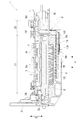
インバータ制御回路30は、制御基板3上に構築されている。また、インバータ装置1は、大電流が流れるために発熱量も大きいパワーモジュール7に接してパワーモジュール7を冷却する冷却モジュール5(図4等参照)を備えて構成されている。以下、図2から図5も参照して、インバータ装置1の構造について詳細に説明する。図2は、インバータ装置1を制御基板3の側から見た斜視図であり、図3は、インバータ装置1を制御基板3とは反対側(冷却モジュール5の側)から見た斜視図である。また、図4は、インバータ装置1を制御基板3に直交する方向(基板直交方向Z)に沿って切断した断面図(図2のIV−IV断面図)である。図5は、インバータ装置1の構造を示す模式的な二面図である。
The
図4に示すように、制御基板3と、パワーモジュール7と、冷却モジュール5とは、制御基板3に直交する方向である基板直交方向Zに見て、少なくとも一部が重複する状態で、制御基板3、パワーモジュール7、冷却モジュール5の順に重ねて配置されている。図2に示すように、パワーモジュール7は、制御基板3に接続されている。図4及び図5に示すように、冷却モジュール5は、パワーモジュール7を載置する面である第1面5aと、第1面5aとは反対側の面である第2面5bとを有している。パワーモジュール7は、冷却モジュール5の第1面5aに接する状態で冷却モジュール5に載置されている。図4に示すように、制御基板3は、パワーモジュール7を間に挟んで、基板締結部材3fにより、冷却モジュール5に固定されている。
As shown in FIG. 4, the
制御基板3とパワーモジュール7と冷却モジュール5とがこのように重ね合わされた状態において、制御基板3は、基板直交方向Zに見て、パワーモジュール7と重複する第1領域31と、重複しない第2領域32とを有している(図5参照)。冷却モジュール5は、パワーモジュール7の冷却を主たる目的として設けられているので、基板直交方向Zに見て、制御基板3の第2領域32は、冷却モジュール5とも重複していない。このため、第2領域32のパワーモジュール7の側には、パワーモジュール7も、冷却モジュール5も存在せず、図4、図5等に示すように、自由空間SPが形成される。本実施形態では、この自由空間SP内に、電流センサ9が配置されている。即ち、電流センサ9は、基板直交方向Zにおいて制御基板3よりもパワーモジュール7の側であって、基板直交方向Zに見て第2領域32に重複する位置に配置されている。換言すれば、電流センサ9は、基板面(XY平面)に沿った方向に見て、パワーモジュール7に重複し、基板直交方向Zに見て、制御基板3の第2領域32と重複する位置に配置されている。尚、電流センサ9は、ハーネス等の電気的接続部材を介して、或いは電流センサ9の端子を制御基板3に実装することによって、制御基板3に電気的に接続される。
In the state where
パワーモジュール7には、交流電力の入出力端子として3相各相に対応した交流端子6(U相端子6u、V相端子6v、W相端子6w:図1参照)が設けられている。各交流端子6には、交流バスバー8(U相バスバー8u、V相バスバー8v、W相バスバー8w:図1参照)が、交流バスバー締結部材8fによって接続されている。交流バスバー8は、交流端子6と、回転電機80のコイル81との電気的接続部材(例えば、不図示の交流機バスバー)とを接続する。図1〜図5等に示す符号“8t”は、そのような電気的接続部材と接続するための接続孔(コイル接続孔)である。複数相の交流電流が流れる交流バスバー8は、非接触で複数相の交流電流を検出する電流センサ9の内部を貫通するように、配設されている。
The
また、交流バスバー8は、図3に示すように、冷却モジュール5の第2面5bに沿って、当該第2面5bに沿う方向では最短距離を通るように配設されている。上述したように、インバータ装置1には、制御基板3、パワーモジュール7、冷却モジュール5が、基板直交方向Zに沿ってこの順に重ねて配置されている。交流バスバー8は、基板直交方向Zに沿って冷却モジュール5の第2面5bに達するまで延伸し、屈曲して、第2面5bに沿ってほぼ最短距離で電流センサ9まで延伸するように配設され、電流センサ9を直線的に貫通している。即ち、交流バスバー8は、交流端子6から電流センサ9までの間の一部の領域において、冷却モジュール5の第2面5bに接するように配置されている。また、交流バスバー8は、交流端子6から電流センサ9までの間の一部の領域において、冷却モジュール5の第2面5bに固定されている。
Further, as shown in FIG. 3, the alternating
冷却モジュール5は、多くの場合、金属などの導電性材料によって構成されているので、冷却モジュール5と交流バスバー8との間は、適切に絶縁されることが好ましい。本実施形態では、熱伝導率及び絶縁性が高い樹脂製の放熱シート15を介して冷却モジュール5に交流バスバー8が固定される(図4参照)。図3及び図4に示すように、交流バスバー8は、樹脂製の固定プレート10によって、冷却モジュール5に固定される。つまり、固定プレート10と冷却モジュール5とによって交流バスバー8を挟み込み、固定プレート10をプレート締結部材10fによって冷却モジュール5に固定する。このように固定プレート10を用いると、交流電流の通流経路となる交流バスバー8に締結孔等を設ける必要がないので、電流の流れを妨げず、また、締結孔等を設けることによる交流バスバー8の強度の低下も抑制することができる。また、冷却モジュール5と交流バスバー8とが、放熱シート15を介して広い面積で密着するために良好な熱伝導が発生し、交流バスバー8を適切に冷却することができる。尚、放熱シート15を用いることなく、例えば、交流バスバー8に、絶縁フィルムや絶縁テープを巻き付けることや、絶縁塗装を施すことによって、冷却モジュール5と絶縁されていてもよい。当然ながら、放熱シート15を用いると共に、絶縁フィルムの巻装や絶縁塗装などによる交流バスバー8自体の絶縁を行ってもよい。
Since the cooling module 5 is often made of a conductive material such as metal, it is preferable that the cooling module 5 and the
ところで、図2、図3の斜視図、及び図5の概念図(模式的二面図)に示すように、制御基板3及びパワーモジュール7の外形は、基板直交方向Zに見て矩形状である。尚、1つのパワーモジュール7が1つのアーム72により構成されているような場合には、制御基板3の基板面(XY平面)に沿った方向に複数のパワーモジュール7が並ぶ領域の外形が矩形状である。ここで、制御基板3及びパワーモジュール7は、基板直交方向Zに見て、制御基板3の各辺(3a,3b,3c,3d:以下“3a〜3d”と表記する場合がある)と、パワーモジュール7の各辺(7a,7b,7c,7d:以下“7a〜7d”と表記する場合がある)とが平行となるように重ねて配置されている。尚、ここで、「平行」とは、完全な平行状態を指すものではなく、概ね45度未満(好ましくは30度未満程度)の角度で、制御基板3の辺と、パワーモジュール7の辺とが沿うような状態であり、辺と辺とが平行状となる状態である。
By the way, as shown in the perspective views of FIG. 2 and FIG. 3 and the conceptual view (schematic two-sided view) of FIG. 5, the external shapes of the
上述したように、パワーモジュール7は、四辺(7a〜7d)の内の一辺に交流端子6を備えている。本実施形態では、第1辺7aに交流端子6が設けられている。制御基板3における第2領域32は、交流端子6が備えられるパワーモジュール7の当該一辺を除く三辺に対して平行(平行状)に配置される制御基板3の三辺の内の少なくとも一辺の側に設けられている。本実施形態では、第1辺7aに交流端子6が設けられているので、第1辺7aを除く三辺(7b,7c,7d)に対して平行(平行状)に配置される三辺(3b,3c,3d)の内の少なくとも一辺である基板第4辺3dの側に、第2領域32が設けられている。
As described above, the
インバータ回路71は、直流と交流との間で電力を変換するので、図1に示すように、パワーモジュール7は、直流電力の入出力端子である直流端子4(正極端子4p,負極端子4n)も有している。パワーモジュール7は、交流端子6が設けられる辺(第1辺7a)とは異なる辺(7b,7c,7d)の何れか一辺に直流端子4を備えている。本実施形態では、交流端子6が設けられる第1辺7aとは異なる第2辺7bに直流端子4が設けられている。
Since the
直流端子4も、基板直交方向Zに見て、制御基板3と重複しない位置に配置されている。第2領域32は、交流端子6が備えられる辺(第1辺7a)及び直流端子4が備えられる辺(第2辺7b)を除く二辺(7c,7d)に対して平行(平行状)に配置される制御基板3の二辺(3c,3d)の内の少なくとも一辺の側に設けられている。本実施形態では、制御基板3において、パワーモジュール7の第1辺7a及び第2辺7bを除く二辺(7c,7d)に対して平行(平行状)に配置される二辺(3c,3d)の内の一辺である基板第4辺3dの側に、第2領域32が設けられている。
The direct
図1〜図3に示すように、直流端子4には、直流バスバー2(正極バスバー2p,負極バスバー2n)が接続されている。直流バスバー2の、直流端子4とは反対側の端部には、直流電源90や直流リンクコンデンサ91などの直流デバイスとの電気的接続部材と接続される直流デバイス接続孔2tが設けられている。例えば、直流リンクコンデンサ91がインバータ装置1とは別に取り付けられる場合には、図1に実線で示す箇所に直流デバイス接続孔2tが設けられる。直流リンクコンデンサ91は、インバータ装置1と一体的に組み付けられても良く、この場合には、図1に破線で示す箇所に直流デバイス接続孔2tが設けられる。
As shown in FIGS. 1 to 3, a DC bus bar 2 (a
冷却モジュール5は、放熱フィン5fを備えた水冷式のヒートシンクである。図3に示す冷媒入出口12を介して冷媒が循環する。また、冷媒流通路11により直流バスバー2もパワーモジュール7と共に冷却可能な構造を有している。直流バスバー2の近傍に直流リンクコンデンサ91や直流電源90などの直流デバイスが配置される場合には、これらの直流デバイスもパワーモジュール7と共に冷却できるようにすることができる。
The cooling module 5 is a water-cooled heat sink provided with
ところで、上記においては、パワーモジュール7の第1辺7aに交流端子6が設けられ、パワーモジュール7の第4辺7dに平行(平行状)に配置される基板第4辺3dの側に、第2領域32が設けられている形態を例示した。しかし、例えば図5における左右を反転させて、パワーモジュール7の第2辺7bに平行(平行状)に配置される基板第2辺3bの側に、第2領域32が設けられていてもよい。上記においては、第2辺7bに直流端子4が配置される形態を例示したが、この場合には、基板直交方向Zに見て、制御基板3と重複しない位置である、第3辺7c或いは第4辺7dに、直流端子4が配置されると好適である。
By the way, in the above, the alternating
上述したように、第2領域32は、パワーモジュール7の第1辺7aを除く三辺(7b,7c,7d)に対して平行(平行状)に配置される制御基板3の三辺(3b,3c,3d)の内の少なくとも一辺の側に設けることができる。従って、図6に示すように、第1辺7aの対辺である第3辺7cに平行(平行状)に配置される基板第3辺3cの側に、第2領域32が設けられてもよい。直流端子4は、上記と同様に、第2辺7bに配置されてもよいし、制御基板3と重複しない位置である第4辺7dに配置されてもよい。
As described above, the
また、第2領域32は、パワーモジュール7の第1辺7aを除く三辺(7b,7c,7d)に対して平行(平行状)に配置される制御基板3の三辺(3b,3c,3d)の内の少なくとも一辺の側に設けられればよいから、該当する二辺或いは三辺の側に設けられてもよい。図7は、パワーモジュール7の第1辺7aを除く三辺(7b,7c,7d)に対して平行(平行状)に配置される制御基板3の三辺(3b,3c,3d)の内の二辺の側に、第2領域32が設けられる形態を例示している。図7では、パワーモジュール7の第1辺7aを除く三辺に対して平行(平行状)に配置される制御基板3の三辺の内の二辺である基板第3辺3c及び基板第4辺3dの側に、第2領域32が設けられる形態を例示している。
In addition, the
さらに、図7における左右を反転させて、基板第2辺3b及び基板第3辺3cの側に、第2領域32が設けられてもよい。尚、この場合には、直流端子4は、基板直交方向Zに見て、制御基板3と重複しない位置である第4辺7dに配置されると好適である。また、図示は省略するが、第2領域32は、基板第2辺3b及び基板第4辺3dの側に設けられてもよい。この場合、直流端子4は、基板直交方向Zに見て、制御基板3と重複しない位置である第3辺7cに配置されると好適である。
Furthermore, the
図8は、パワーモジュール7の第1辺7aを除く三辺(7b,7c,7d)に対して平行(平行状)に配置される制御基板3の三辺(基板第2辺3b、基板第3辺3c、基板第4辺3d)の側に、第2領域32が設けられる形態を例示している。この場合、基板直交方向Zに見て、制御基板3と重複しない位置は、第1辺7aのみとなるから、交流端子6が設けられる辺(第1辺7a)とは異なる辺に直流端子4を設けることはできない。基板直交方向Zに見て、制御基板3と重複しないように直流端子4を設ける場合には、交流端子6が設けられる辺と同じ辺(第1辺7a)に直流端子4が設けられる。また、交流端子6が設けられる辺と同じ辺(第1辺7a)に、直流端子4を設けない場合には、基板直交方向Zに見て制御基板3とは重複する状態で直流端子4が設けられる。
FIG. 8 shows three sides (a
尚、図9及び図10は、図1〜図5に例示した態様に対する比較例を示している。図9は第1比較例であり、第10は第2比較例である。図9は、電流センサ9が、制御基板3の第2領域32と基板直交方向Zに見て重複する位置ではなく、基板直交方向Zに見てパワーモジュール7とも制御基板3とも重複しない位置に配置されている。図5等に例示した態様と比較して、図9に例示した第1比較例では、交流バスバー8の長さは短くなっている。しかし、基板直交方向Zに見たインバータ装置1の投影面積は、第1比較例の方が大きくなっており、インバータ装置1の小型化の妨げとなるおそれがある。また、第1比較例では、交流バスバー8を冷却モジュール5によって冷却することも困難である。
9 and 10 show a comparative example to the embodiment illustrated in FIGS. 1 to 5. FIG. 9 is a first comparative example, and 10 is a second comparative example. In FIG. 9, the
図10に示す第2比較例では、電流センサ9は、図5等に例示した態様と同様に制御基板3の第2領域32と基板直交方向Zに見て重複する位置に配置されている。この点では、基板直交方向Zに見たインバータ装置1の投影面積は、図5等に例示した態様と等価である。しかし、交流バスバー8は、冷却モジュール5の第2面5bと接するようには配設されておらず、基板面(XY平面)に沿った方向に、パワーモジュール7を迂回して配設されている。このため、図5等に例示した態様に比べて第2比較例では、基板直交方向Zに見たインバータ装置1の投影面積が大きくなっている。また、比較的、配線経路が長くなる交流バスバー8は、電気抵抗も大きくなるから、発熱量も増大するが、第1比較例と同様に交流バスバー8を冷却モジュール5によって冷却することは困難である。また、そのように長尺の交流バスバー8が、冷却モジュール5によって固定されないため、図5等に例示した態様に比べて機械的振動も抑制されない。このため、図5等に示す態様に比べて、第2比較例では発熱や機械的振動に伴う交流バスバー8の金属疲労が大きくなる傾向がある。
In the second comparative example shown in FIG. 10, the
以上、種々の態様を例示して説明したが、各態様は、それぞれ単独で適用されるものに限られず、矛盾が生じない限り、組み合わせて適用することも可能である。また、本明細書において開示された態様は全ての点で単なる例示に過ぎない。従って、本開示の趣旨を逸脱しない範囲内で、適宜、種々の改変を行うことが可能である。 As mentioned above, although the various aspects were illustrated and explained, each aspect is not restricted to what is applied individually, respectively, and as long as no contradiction arises, it is also possible to apply in combination. Also, the aspects disclosed herein are merely exemplary in all respects. Therefore, various modifications can be made as appropriate without departing from the spirit of the present disclosure.
〔実施形態の概要〕
以下、上記において説明したインバータ装置(1)の概要について簡単に説明する。
Outline of Embodiment
Hereinafter, the outline of the inverter device (1) described above will be briefly described.
1つの態様として、直流電力と複数相の交流電力との間で電力を変換するインバータ回路(71)を備えたインバータ装置(1)は、
前記インバータ回路(71)を構成するスイッチング素子(73)を備えたパワーモジュール(7)と、
前記パワーモジュール(7)に接して前記パワーモジュール(7)を冷却する冷却モジュール(5)と、
前記スイッチング素子(73)をスイッチング制御する制御回路(30)を備えた制御基板(3)と、
前記パワーモジュール(7)の交流電力の入出力端子である交流端子(6)に接続される交流バスバー(8)と、
前記交流バスバー(8)を流れる複数相の交流電流を検出する電流センサ(9)と、
を備え、
前記制御基板(3)と、前記パワーモジュール(7)と、前記冷却モジュール(5)とは、前記制御基板(3)に直交する方向である基板直交方向(Z)に見て、少なくとも一部が重複する状態で、前記制御基板(3)、前記パワーモジュール(7)、前記冷却モジュール(5)の順に重ねて配置され、
前記制御基板(3)は、前記基板直交方向(Z)に見て、前記パワーモジュール(7)と重複する第1領域(31)と、重複しない第2領域(32)とを有し、
前記交流端子(6)は、前記基板直交方向(Z)に見て、前記制御基板(3)と重複しない位置に配置され、
前記電流センサ(9)は、前記基板直交方向(Z)において前記制御基板(3)よりも前記パワーモジュール(7)の側であって、前記基板直交方向(Z)に見て前記第2領域(32)に重複する位置に配置され、
前記冷却モジュール(5)は、前記パワーモジュール(7)を載置する面である第1面(5a)と、前記第1面とは反対側の面である第2面(5b)とを有し、
前記交流バスバー(8)は、前記交流端子(6)から前記電流センサ(9)までの間の一部の領域において、前記第2面(5b)に接するように配置されると共に、前記冷却モジュール(5)に固定されている。
As one aspect, an inverter device (1) including an inverter circuit (71) that converts power between DC power and AC power of multiple phases is:
A power module (7) comprising a switching element (73) constituting the inverter circuit (71);
A cooling module (5) for cooling the power module (7) in contact with the power module (7);
A control board (3) provided with a control circuit (30) for switching control of the switching element (73);
An alternating current bus bar (8) connected to an alternating current terminal (6) which is an input / output terminal of alternating current power of the power module (7);
A current sensor (9) for detecting alternating currents of a plurality of phases flowing through the alternating current bus bar (8);
Equipped with
The control substrate (3), the power module (7), and the cooling module (5) are at least partially viewed in a substrate orthogonal direction (Z) which is a direction orthogonal to the control substrate (3). Are arranged in the order of the control board (3), the power module (7) and the cooling module (5),
The control substrate (3) has a first area (31) overlapping with the power module (7) and a second area (32) not overlapping with the power module (7) in the substrate orthogonal direction (Z),
The AC terminal (6) is disposed at a position not overlapping the control substrate (3) when viewed in the substrate orthogonal direction (Z),
The current sensor (9) is closer to the power module (7) than the control substrate (3) in the substrate orthogonal direction (Z), and the second region when viewed in the substrate orthogonal direction (Z) (32) is placed at the overlapping position,
The cooling module (5) has a first surface (5a) which is a surface on which the power module (7) is mounted, and a second surface (5b) which is a surface opposite to the first surface. And
The AC bus bar (8) is disposed in contact with the second surface (5b) in a partial region between the AC terminal (6) and the current sensor (9), and the cooling module It is fixed to (5).
この構成によれば、制御基板(3)の第2領域(32)の裏側(パワーモジュール(7)の側)に、制御基板(3)の面方向に沿ってパワーモジュール(7)と並ぶように、電流センサ(9)が配置される。第2領域(32)の裏側の空間(SP)は、パワーモジュール(7)とは重複せず、パワーモジュール(7)を冷却する冷却モジュール(5)もその部分には設けられる必要がないから、当該空間(SP)は、余剰空間ということができる。そのような余剰空間(SP)に、電流センサ(9)が配置されるので、インバータ装置(1)を構成するに当たって、空間の利用効率が良くなる。交流バスバー(8)は、パワーモジュール(7)や制御基板(3)を、基板面方向(XY平面に沿った方向)に延びて迂回するように配設されるのではなく、冷却モジュール(5)の第2面(5b)に接するように配置され、且つ冷却モジュール(5)に固定されている。このため、パワーモジュール(7)や制御基板(3)を迂回するよりも交流バスバー(8)の長さが短縮されて電気抵抗の増加に伴う温度上昇が抑制され、また、冷却モジュール(5)への固定によって機械的振動も抑制される。このように、本構成によれば、インバータ装置(1)を構成する部材を効率的に配置して、インバータ装置(1)の全体を小型化できる。 According to this configuration, on the back side (the power module (7) side) of the second region (32) of the control substrate (3), the power module (7) is aligned along the surface direction of the control substrate (3) , A current sensor (9) is arranged. The space (SP) on the back side of the second area (32) does not overlap with the power module (7), and the cooling module (5) for cooling the power module (7) does not have to be provided in that part either The space (SP) can be said to be surplus space. Since the current sensor (9) is disposed in such an extra space (SP), the space utilization efficiency is improved in configuring the inverter device (1). The alternating current bus bar (8) is not disposed to extend and detour the power module (7) and the control board (3) in the substrate surface direction (direction along the XY plane). Are arranged in contact with the second surface (5b) of the) and fixed to the cooling module (5). Therefore, the length of the alternating current bus bar (8) is shortened rather than bypassing the power module (7) or the control board (3), so that the temperature rise due to the increase of the electrical resistance is suppressed, and the cooling module (5) The mechanical vibration is also suppressed by the fixation to the housing. As described above, according to the present configuration, the members constituting the inverter device (1) can be efficiently disposed, and the entire size of the inverter device (1) can be reduced.
1つの態様として、前記制御基板(3)及び前記パワーモジュール(7)の外形が、前記基板直交方向(Z)に見て矩形状であり、前記制御基板(3)及び前記パワーモジュール(7)は、前記基板直交方向(Z)に見て、前記制御基板(3)の各辺(3a,3b,3c,3d)と前記パワーモジュール(7)の各辺(7a,7b,7c,7d)とが平行となるように重ねて配置され、前記パワーモジュール(7)は、四辺の内の一辺(7a)に前記交流端子(6)を備え、前記第2領域(32)は、前記交流端子(6)が備えられる前記パワーモジュールの当該一辺(7a)を除く三辺(7b,7c,7d)に対して平行に配置される前記制御基板(3)の三辺(3b,7c,7d)の内の少なくとも一辺の側に設けられていると好適である。 As one aspect, the external shape of the control substrate (3) and the power module (7) is rectangular when viewed in the substrate orthogonal direction (Z), and the control substrate (3) and the power module (7) Are the sides (3a, 3b, 3c, 3d) of the control substrate (3) and the sides (7a, 7b, 7c, 7d) of the power module (7), as viewed in the substrate orthogonal direction (Z). And the power module (7) includes the AC terminal (6) on one side (7a) of the four sides, and the second region (32) includes the AC terminal. (6) The three sides (3b, 7c, 7d) of the control substrate (3) disposed parallel to the three sides (7b, 7c, 7d) except the one side (7a) of the power module provided Provided on at least one side of the .
尚、ここで、「平行」とは、完全な平行状態を指すものではなく、制御基板3の辺と、パワーモジュール7の辺とがほぼ平行するような状態である。例えば、概ね45度未満(好ましくは30度未満程度)の角度で、制御基板3の辺と、パワーモジュール7の辺とが沿うような状態であり、辺と辺とが平行状となる状態ということもできる。交流バスバー(8)は、交流機器との電気的接続部材と接続するために、基板直交方向(Z)において、制御基板(3)と重複しない部位を有するように配置する必要がある。このため、制御基板(3)は、交流バスバー(8)が突出する方向とは異なる方向に第2領域(32)を有するように配置されることが好ましい。
Here, “parallel” does not refer to a completely parallel state, but is a state in which the side of the
また、1つの態様として、前記パワーモジュールが、前記交流端子(6)が設けられる辺である第1辺(7a)とは異なる辺である第2辺(7b)に、直流電力の入出力端子である直流端子(4)を備える場合、前記直流端子(4)が、前記基板直交方向(Z)に見て、前記制御基板(3)と重複しない位置に配置され、前記第2領域(32)が、前記制御基板(3)において、前記パワーモジュール(7)の前記第1辺(7a)及び前記第2辺(7b)を除く二辺(7c,7d)に対して平行に配置される辺(3c,3d)の内の少なくとも一辺の側に設けられていると好適である。 In one aspect, an input / output terminal for DC power is provided to the second side (7b), which is a side different from the first side (7a), which is the side where the AC terminal (6) is provided, as the power module. When the DC terminal (4) is provided, the DC terminal (4) is disposed at a position not overlapping the control substrate (3) when viewed in the substrate orthogonal direction (Z), and the second region (32) Is disposed parallel to two sides (7c, 7d) of the control board (3) excluding the first side (7a) and the second side (7b) of the power module (7). It is preferable to provide at least one side of the sides (3c, 3d).
交流端子(6)と同様に、直流端子(4)にもバスバー(直流バスバー(2))や、直流素子(例えば平滑コンデンサ)、直流機器(例えば直流電源(90))との接続部材が接続されることが多い。このため、交流端子(6)が配置されて交流バスバー(8)が突出する第1辺(7a)と同様に、直流端子(4)が配置される第2辺(7b)も、基板直交方向(Z)において制御基板(3)とは重複しないことが好ましい。従って、制御基板(3)の第2領域(32)は、第1辺(7a)及び第2辺(7b)を除く二辺(7c,7d)に対して平行(平行状)に配置される辺(3c,3d)の側に設けられることが好ましい。 Similar to the AC terminal (6), the DC terminal (4) is also connected to the bus bar (DC bus bar (2)), the DC element (for example, smoothing capacitor), and the connection member for DC devices (for example, DC power supply (90) It is often done. Therefore, like the first side (7a) where the AC terminal (6) is arranged and the AC bus bar (8) protrudes, the second side (7b) where the DC terminal (4) is arranged is also in the substrate orthogonal direction Preferably, the control substrate (3) does not overlap in (Z). Therefore, the second region (32) of the control substrate (3) is disposed parallel (parallel to) the two sides (7c, 7d) excluding the first side (7a) and the second side (7b) Preferably, they are provided on the side (3c, 3d).
また、1つの態様として、前記交流バスバー(8)は、放熱シート(15)を介して前記冷却モジュールに固定されていると好適である。放熱シート(15)を介することにより、交流バスバー(8)において生じる熱を適切に冷却モジュール(5)に伝達させることができる。共通の冷却モジュール(5)によって、パワーモジュール(7)と交流バスバー(8)とを冷却することができ、インバータ装置(1)の全体を小型化できる。 Further, as one aspect, it is preferable that the alternating current bus bar (8) is fixed to the cooling module via a heat dissipation sheet (15). The heat generated in the alternating current bus bar (8) can be properly transmitted to the cooling module (5) through the heat dissipation sheet (15). The power module (7) and the alternating current bus bar (8) can be cooled by the common cooling module (5), and the whole of the inverter device (1) can be miniaturized.
1 :インバータ装置
3 :制御基板
4 :直流端子
5 :冷却モジュール
5a :第1面
5b :第2面
6 :交流端子
7 :パワーモジュール
7a :第1辺
7b :第2辺
8 :交流バスバー
9 :電流センサ
15 :放熱シート
30 :インバータ制御回路(制御回路)
31 :第1領域
32 :第2領域
71 :インバータ回路
73 :スイッチング素子
100 :上位制御装置
Z :基板直交方向
1: inverter device 3: control board 4: direct current terminal 5: cooling
31: first area 32: second area 71: inverter circuit 73: switching element 100: host controller Z: substrate orthogonal direction
Claims (4)
前記インバータ回路を構成するスイッチング素子を備えたパワーモジュールと、
前記パワーモジュールに接して前記パワーモジュールを冷却する冷却モジュールと、
前記スイッチング素子をスイッチング制御する制御回路を備えた制御基板と、
前記パワーモジュールの交流電力の入出力端子である交流端子に接続される交流バスバーと、
前記交流バスバーを流れる複数相の交流電流を検出する電流センサと、
を備え、
前記制御基板と、前記パワーモジュールと、前記冷却モジュールとは、前記制御基板に直交する方向である基板直交方向に見て、少なくとも一部が重複する状態で、前記制御基板、前記パワーモジュール、前記冷却モジュールの順に重ねて配置され、
前記制御基板は、前記基板直交方向に見て、前記パワーモジュールと重複する第1領域と、重複しない第2領域とを有し、
前記交流端子は、前記基板直交方向に見て、前記制御基板と重複しない位置に配置され、
前記電流センサは、前記基板直交方向において前記制御基板よりも前記パワーモジュールの側であって、前記基板直交方向に見て前記第2領域に重複する位置に配置され、
前記冷却モジュールは、前記パワーモジュールを載置する面である第1面と、前記第1面とは反対側の面である第2面とを有し、
前記交流バスバーは、前記交流端子から前記電流センサまでの間の一部の領域において、前記第2面に接するように配置されると共に、前記冷却モジュールに固定されている、
インバータ装置。 An inverter device comprising an inverter circuit for converting power between DC power and AC power of multiple phases, comprising:
A power module provided with a switching element forming the inverter circuit;
A cooling module for cooling the power module in contact with the power module;
A control substrate provided with a control circuit that performs switching control of the switching element;
An AC bus bar connected to an AC terminal which is an input / output terminal of AC power of the power module;
A current sensor for detecting a plurality of phases of alternating current flowing through the alternating current bus bar;
Equipped with
The control substrate, the power module, and the power module in a state in which at least a portion of the control substrate, the power module, and the cooling module overlap when viewed in a substrate orthogonal direction which is a direction orthogonal to the control substrate. The cooling modules are stacked and arranged in order
The control substrate has a first region overlapping the power module and a second region not overlapping when viewed in the substrate orthogonal direction.
The AC terminal is disposed at a position not overlapping with the control substrate when viewed in the substrate orthogonal direction.
The current sensor is disposed at a position closer to the power module than the control substrate in the substrate orthogonal direction, and at a position overlapping the second region when viewed in the substrate orthogonal direction.
The cooling module has a first surface which is a surface on which the power module is mounted, and a second surface which is a surface opposite to the first surface.
The AC bus bar is disposed in contact with the second surface in a partial region between the AC terminal and the current sensor, and is fixed to the cooling module.
Inverter device.
前記制御基板及び前記パワーモジュールは、前記基板直交方向に見て、前記制御基板の各辺と前記パワーモジュールの各辺とが平行となるように重ねて配置され、
前記パワーモジュールは、四辺の内の一辺に前記交流端子を備え、
前記第2領域は、前記交流端子が備えられる前記パワーモジュールの当該一辺を除く三辺に対して平行に配置される前記制御基板の三辺の内の少なくとも一辺の側に設けられている、
請求項1に記載のインバータ装置。 The external shapes of the control substrate and the power module are rectangular when viewed in the substrate orthogonal direction,
The control substrate and the power module are disposed in an overlapping manner so that each side of the control substrate and each side of the power module are parallel to each other when viewed in the substrate orthogonal direction.
The power module includes the AC terminal on one side of four sides.
The second region is provided on at least one of three sides of the control board disposed parallel to three sides of the power module including the AC terminal except the one side.
The inverter device according to claim 1.
前記直流端子は、前記基板直交方向に見て、前記制御基板と重複しない位置に配置され、
前記第2領域は、前記制御基板において、前記パワーモジュールの前記第1辺及び前記第2辺を除く二辺に対して平行に配置される辺の内の少なくとも一辺の側に設けられている、
請求項2に記載のインバータ装置。 The power module includes a DC terminal, which is an input / output terminal for DC power, on a second side which is a side different from the first side which is the side where the AC terminal is provided,
The DC terminal is disposed at a position not overlapping the control substrate when viewed in the substrate orthogonal direction.
The second region is provided on at least one side of the sides arranged in parallel to two sides of the power module except the first side and the second side in the control substrate.
The inverter device according to claim 2.
Priority Applications (1)
| Application Number | Priority Date | Filing Date | Title |
|---|---|---|---|
| JP2016032908A JP6515836B2 (en) | 2016-02-24 | 2016-02-24 | Inverter device |
Applications Claiming Priority (1)
| Application Number | Priority Date | Filing Date | Title |
|---|---|---|---|
| JP2016032908A JP6515836B2 (en) | 2016-02-24 | 2016-02-24 | Inverter device |
Publications (2)
| Publication Number | Publication Date |
|---|---|
| JP2017153228A JP2017153228A (en) | 2017-08-31 |
| JP6515836B2 true JP6515836B2 (en) | 2019-05-22 |
Family
ID=59738540
Family Applications (1)
| Application Number | Title | Priority Date | Filing Date |
|---|---|---|---|
| JP2016032908A Active JP6515836B2 (en) | 2016-02-24 | 2016-02-24 | Inverter device |
Country Status (1)
| Country | Link |
|---|---|
| JP (1) | JP6515836B2 (en) |
Families Citing this family (3)
| Publication number | Priority date | Publication date | Assignee | Title |
|---|---|---|---|---|
| CN112313869A (en) * | 2018-06-19 | 2021-02-02 | 株式会社电装 | Power conversion device |
| JP6908004B2 (en) * | 2018-06-19 | 2021-07-21 | 株式会社デンソー | Power converter |
| JP6973313B2 (en) * | 2018-07-11 | 2021-11-24 | 株式会社デンソー | Power converter |
Family Cites Families (6)
| Publication number | Priority date | Publication date | Assignee | Title |
|---|---|---|---|---|
| JP3734122B2 (en) * | 1997-10-22 | 2006-01-11 | 株式会社デンソー | Three-phase inverter circuit module |
| US7579805B2 (en) * | 2004-01-26 | 2009-08-25 | Hitachi, Ltd. | Semiconductor device |
| JP2008220060A (en) * | 2007-03-05 | 2008-09-18 | Mitsubishi Electric Corp | Power conversion device and current sensor |
| JP5268880B2 (en) * | 2009-12-24 | 2013-08-21 | 日立オートモティブシステムズ株式会社 | Power converter |
| JP6139366B2 (en) * | 2013-10-09 | 2017-05-31 | 日立オートモティブシステムズ株式会社 | Power converter |
| JP5978324B2 (en) * | 2015-01-21 | 2016-08-24 | 日立オートモティブシステムズ株式会社 | Power converter |
-
2016
- 2016-02-24 JP JP2016032908A patent/JP6515836B2/en active Active
Also Published As
| Publication number | Publication date |
|---|---|
| JP2017153228A (en) | 2017-08-31 |
Similar Documents
| Publication | Publication Date | Title |
|---|---|---|
| JP5622043B2 (en) | Inverter device | |
| JP5534352B2 (en) | Inverter device | |
| JP5506740B2 (en) | Power converter | |
| JP4106061B2 (en) | Power unit device and power conversion device | |
| JP4719187B2 (en) | Semiconductor device cooling structure | |
| JP5534353B2 (en) | Inverter device | |
| JP5957396B2 (en) | Double-sided cooling power converter | |
| WO2013015106A1 (en) | Power conversion device | |
| JP5488638B2 (en) | Power converter | |
| US10798855B2 (en) | Power conversion device | |
| JP2006340569A (en) | Power unit | |
| JP6677346B2 (en) | Inverter unit | |
| JP6515836B2 (en) | Inverter device | |
| WO2013065849A1 (en) | Inverter device | |
| WO2020218014A1 (en) | Power conversion device | |
| WO2015040902A1 (en) | Power semiconductor module and power converter using same | |
| JP6181136B2 (en) | Power converter | |
| JP2004031590A (en) | Semiconductor device | |
| JP2018022731A (en) | Power module and power control unit | |
| JP6673246B2 (en) | Semiconductor device | |
| WO2017002693A1 (en) | Electric compressor | |
| JP6368763B2 (en) | Power converter | |
| JP6754387B2 (en) | Power converter | |
| WO2013065847A1 (en) | Inverter device | |
| US20230395457A1 (en) | Power Semiconductor Device, Power Conversion Device, and Electric System |
Legal Events
| Date | Code | Title | Description |
|---|---|---|---|
| A621 | Written request for application examination |
Free format text: JAPANESE INTERMEDIATE CODE: A621 Effective date: 20180606 |
|
| TRDD | Decision of grant or rejection written | ||
| A01 | Written decision to grant a patent or to grant a registration (utility model) |
Free format text: JAPANESE INTERMEDIATE CODE: A01 Effective date: 20190319 |
|
| A977 | Report on retrieval |
Free format text: JAPANESE INTERMEDIATE CODE: A971007 Effective date: 20190320 |
|
| A61 | First payment of annual fees (during grant procedure) |
Free format text: JAPANESE INTERMEDIATE CODE: A61 Effective date: 20190401 |
|
| R150 | Certificate of patent or registration of utility model |
Ref document number: 6515836 Country of ref document: JP Free format text: JAPANESE INTERMEDIATE CODE: R150 |