JP6515115B2 - Electrically adjustable lens and lens system - Google Patents
Electrically adjustable lens and lens system Download PDFInfo
- Publication number
- JP6515115B2 JP6515115B2 JP2016555831A JP2016555831A JP6515115B2 JP 6515115 B2 JP6515115 B2 JP 6515115B2 JP 2016555831 A JP2016555831 A JP 2016555831A JP 2016555831 A JP2016555831 A JP 2016555831A JP 6515115 B2 JP6515115 B2 JP 6515115B2
- Authority
- JP
- Japan
- Prior art keywords
- electro
- electrodes
- electrode
- layer
- optic layer
- Prior art date
- Legal status (The legal status is an assumption and is not a legal conclusion. Google has not performed a legal analysis and makes no representation as to the accuracy of the status listed.)
- Active
Links
- 230000005284 excitation Effects 0.000 claims description 110
- 230000003287 optical effect Effects 0.000 claims description 79
- 230000010287 polarization Effects 0.000 claims description 48
- 230000007704 transition Effects 0.000 claims description 41
- 239000004973 liquid crystal related substance Substances 0.000 claims description 30
- 239000004020 conductor Substances 0.000 claims description 12
- 238000004519 manufacturing process Methods 0.000 claims description 11
- 230000001419 dependent effect Effects 0.000 claims description 9
- 238000000034 method Methods 0.000 claims description 8
- 239000000758 substrate Substances 0.000 description 26
- 230000003068 static effect Effects 0.000 description 24
- 230000008859 change Effects 0.000 description 18
- 230000010363 phase shift Effects 0.000 description 12
- 230000004044 response Effects 0.000 description 8
- 230000000694 effects Effects 0.000 description 7
- 239000000463 material Substances 0.000 description 7
- 238000013459 approach Methods 0.000 description 5
- 239000000382 optic material Substances 0.000 description 5
- 238000013139 quantization Methods 0.000 description 5
- 238000012937 correction Methods 0.000 description 4
- 238000005538 encapsulation Methods 0.000 description 4
- 230000008901 benefit Effects 0.000 description 3
- 230000005684 electric field Effects 0.000 description 3
- 239000011810 insulating material Substances 0.000 description 3
- 230000000737 periodic effect Effects 0.000 description 3
- 239000012780 transparent material Substances 0.000 description 3
- 230000009286 beneficial effect Effects 0.000 description 2
- 239000002131 composite material Substances 0.000 description 2
- 238000013461 design Methods 0.000 description 2
- 238000009826 distribution Methods 0.000 description 2
- 239000011521 glass Substances 0.000 description 2
- 238000009499 grossing Methods 0.000 description 2
- 238000007373 indentation Methods 0.000 description 2
- 238000012886 linear function Methods 0.000 description 2
- 239000011159 matrix material Substances 0.000 description 2
- 229920000642 polymer Polymers 0.000 description 2
- 230000004256 retinal image Effects 0.000 description 2
- 238000000926 separation method Methods 0.000 description 2
- 239000004986 Cholesteric liquid crystals (ChLC) Substances 0.000 description 1
- 239000004642 Polyimide Substances 0.000 description 1
- XUIMIQQOPSSXEZ-UHFFFAOYSA-N Silicon Chemical compound [Si] XUIMIQQOPSSXEZ-UHFFFAOYSA-N 0.000 description 1
- 239000013543 active substance Substances 0.000 description 1
- 239000000853 adhesive Substances 0.000 description 1
- 230000001070 adhesive effect Effects 0.000 description 1
- 238000000149 argon plasma sintering Methods 0.000 description 1
- 238000003491 array Methods 0.000 description 1
- 230000003098 cholesteric effect Effects 0.000 description 1
- 150000001875 compounds Chemical class 0.000 description 1
- 230000003247 decreasing effect Effects 0.000 description 1
- 238000000151 deposition Methods 0.000 description 1
- 238000010586 diagram Methods 0.000 description 1
- 239000000499 gel Substances 0.000 description 1
- 230000005484 gravity Effects 0.000 description 1
- AMGQUBHHOARCQH-UHFFFAOYSA-N indium;oxotin Chemical compound [In].[Sn]=O AMGQUBHHOARCQH-UHFFFAOYSA-N 0.000 description 1
- 239000012212 insulator Substances 0.000 description 1
- 238000012986 modification Methods 0.000 description 1
- 230000004048 modification Effects 0.000 description 1
- 230000002093 peripheral effect Effects 0.000 description 1
- 229920001721 polyimide Polymers 0.000 description 1
- 230000008569 process Effects 0.000 description 1
- 238000012545 processing Methods 0.000 description 1
- 230000001902 propagating effect Effects 0.000 description 1
- 210000001747 pupil Anatomy 0.000 description 1
- 210000001525 retina Anatomy 0.000 description 1
- 238000005070 sampling Methods 0.000 description 1
- 239000000565 sealant Substances 0.000 description 1
- 238000007789 sealing Methods 0.000 description 1
- 239000007787 solid Substances 0.000 description 1
- 125000006850 spacer group Chemical group 0.000 description 1
- 238000012546 transfer Methods 0.000 description 1
- 230000000007 visual effect Effects 0.000 description 1
Images


Classifications
-
- G—PHYSICS
- G02—OPTICS
- G02F—OPTICAL DEVICES OR ARRANGEMENTS FOR THE CONTROL OF LIGHT BY MODIFICATION OF THE OPTICAL PROPERTIES OF THE MEDIA OF THE ELEMENTS INVOLVED THEREIN; NON-LINEAR OPTICS; FREQUENCY-CHANGING OF LIGHT; OPTICAL LOGIC ELEMENTS; OPTICAL ANALOGUE/DIGITAL CONVERTERS
- G02F1/00—Devices or arrangements for the control of the intensity, colour, phase, polarisation or direction of light arriving from an independent light source, e.g. switching, gating or modulating; Non-linear optics
- G02F1/01—Devices or arrangements for the control of the intensity, colour, phase, polarisation or direction of light arriving from an independent light source, e.g. switching, gating or modulating; Non-linear optics for the control of the intensity, phase, polarisation or colour
- G02F1/13—Devices or arrangements for the control of the intensity, colour, phase, polarisation or direction of light arriving from an independent light source, e.g. switching, gating or modulating; Non-linear optics for the control of the intensity, phase, polarisation or colour based on liquid crystals, e.g. single liquid crystal display cells
- G02F1/133—Constructional arrangements; Operation of liquid crystal cells; Circuit arrangements
- G02F1/1333—Constructional arrangements; Manufacturing methods
- G02F1/1343—Electrodes
- G02F1/134309—Electrodes characterised by their geometrical arrangement
-
- G—PHYSICS
- G02—OPTICS
- G02F—OPTICAL DEVICES OR ARRANGEMENTS FOR THE CONTROL OF LIGHT BY MODIFICATION OF THE OPTICAL PROPERTIES OF THE MEDIA OF THE ELEMENTS INVOLVED THEREIN; NON-LINEAR OPTICS; FREQUENCY-CHANGING OF LIGHT; OPTICAL LOGIC ELEMENTS; OPTICAL ANALOGUE/DIGITAL CONVERTERS
- G02F1/00—Devices or arrangements for the control of the intensity, colour, phase, polarisation or direction of light arriving from an independent light source, e.g. switching, gating or modulating; Non-linear optics
- G02F1/29—Devices or arrangements for the control of the intensity, colour, phase, polarisation or direction of light arriving from an independent light source, e.g. switching, gating or modulating; Non-linear optics for the control of the position or the direction of light beams, i.e. deflection
- G02F1/294—Variable focal length devices
Landscapes
- Physics & Mathematics (AREA)
- Nonlinear Science (AREA)
- General Physics & Mathematics (AREA)
- Optics & Photonics (AREA)
- Geometry (AREA)
- Mathematical Physics (AREA)
- Chemical & Material Sciences (AREA)
- Crystallography & Structural Chemistry (AREA)
- Liquid Crystal (AREA)
- Optical Modulation, Optical Deflection, Nonlinear Optics, Optical Demodulation, Optical Logic Elements (AREA)
Description
本発明は、一般的に光学装置に関し、特に電気的に調整可能なレンズに関するものである。 The present invention relates generally to optical devices, and more particularly to electrically adjustable lenses.
本出願は2014年3月13日出願の米国暫定特許出願61/952,226(特許文献1);2014年3月23日出願の米国暫定特許出願61/969,190(特許文献2);2014年3月31日出願の米国暫定特許出願61/972,445(特許文献3)の恩恵を主張する。本出願はまた、2013年9月30日出願のPCT特許出願PCT/IB2013/058989(WO2014/049577として公表;特許文献4)の部分継続出願であり、その出願は2012年9月30日出願の米国暫定特許出願61/707,962(特許文献5)の恩恵を主張する。これら関連出願のすべては、ここに参照として採り入れられる。 This application is related to U.S. Provisional Patent Application 61 / 952,226, filed March 13, 2014; U.S. Provisional Patent Application 61 / 969,190, filed March 23, 2014; Claims the benefit of U.S. Provisional Patent Application No. 61 / 972,445, filed March 31, 2012. This application is also a continuation-in-part of PCT patent application PCT / IB2013 / 058989 (published as WO 2014/049577; filed in Sept. 30, 2013; Patent Document 4), which application is filed on Sept. 30, 2012 Claims the benefit of US Provisional Patent Application 61 / 707,962. All of these related applications are incorporated herein by reference.
調整可能レンズは、その焦点距離、および/または光軸の位置などの光学特性が、一般的に電気制御により使用中に調節できる、光学要素である。このようなレンズは広範囲の用途に使用できる。例えば、米国特許7,475,985(特許文献6)、それはここに参照として採り入れられるが、は視力矯正の目的のための電気活性レンズの使用について記載している。 An adjustable lens is an optical element whose optical properties, such as its focal length and / or the position of the optical axis, can generally be adjusted during use by means of electrical control. Such lenses can be used in a wide variety of applications. For example, US Pat. No. 7,475,985, which is incorporated herein by reference, describes the use of electroactive lenses for the purpose of vision correction.
電気調整可能なレンズは、一般的に適合する電気光学的材料の薄い層を含み、その局所的実効屈折率は材料を横断して印加される電圧の関数として変化する。電極または電極配列は、局所的に屈折率を所望の値に調節するために所望の電圧を印加するのに使用される。液晶はこの目的のために最も頻繁に使用される電気光学的材料である。(印加電圧が分子を回転させ、それが複屈折軸を変化させ、それにより実効屈折率を変化させる。)しかし、高分子ゲルのような類似の電気光学的特性を有する他の材料もこの目的に使用可能である。 An electrically tunable lens generally comprises a thin layer of compatible electro-optical material, the local effective refractive index of which varies as a function of the voltage applied across the material. The electrode or electrode arrangement is used to apply the desired voltage to adjust the refractive index to the desired value locally. Liquid crystals are the most frequently used electro-optical materials for this purpose. (The applied voltage rotates the molecule, which changes the birefringence axis, thereby changing the effective refractive index.) However, other materials with similar electro-optical properties, such as polymer gels, also serve this purpose It can be used for
いくつかの調整可能レンズ設計は、電極配列を使用して、液晶ディスプレイに使用される画素格子の類に似た、液晶中の画素格子を定義している。個々の画素の屈折率は電気的に制御され、所望の位相変調プロファイルを与える。(「位相変調プロファイル」という用語は本明細書および請求項においては、調整可能レンズの電気光学層の領域に亘る、局所的に変化する実効屈折率の結果としての、その層を通過する光に適用される局所位相偏移の分布を意味する。この種の格子配列を使用するレンズは、例えば上記の米国特許7,475,985(特許文献6)に記載されている。 Some adjustable lens designs use electrode arrays to define pixel grids in liquid crystals, similar to the class of pixel grids used in liquid crystal displays. The refractive indices of the individual pixels are electrically controlled to provide the desired phase modulation profile. (The term “phase modulation profile” as used herein and in the claims refers to light passing through that layer as a result of the locally varying effective refractive index over the area of the electro-optical layer of the tunable lens By means of the distribution of the applied local phase shifts, lenses using this type of grating arrangement are described, for example, in the above-mentioned US Pat. No. 7,475,985.
上記のPCT特許出願公報WO2014/049577(特許文献4)は、光学装置であって、電気光学層の活性領域内の任意の所与の位置において局所実効屈折率を有する、液晶のような、電気光学層を有し、実効屈折率は所与の位置における電気光学層を横断して印加される電圧波形により決定される光学装置を記載している。平行な導電性ストライプを有する、活性領域の上に伸長する励起電極の配列が電気光学層の片側または両側に配置される。制御回路は、それぞれの制御電圧波形をその励起電極に印加し、そして、電気光学層の位相変調プロファイルを生成するため、励起電極に印加されるそれぞれの制御電圧波形を同時に変調するように構成される。 The PCT patent application publication WO 2014/049577 mentioned above is an optical device, such as liquid crystal, having a local effective refractive index at any given position within the active region of the electro-optical layer. It describes an optical device having an optical layer, the effective refractive index being determined by the voltage waveform applied across the electro-optical layer at a given location. An array of excitation electrodes extending above the active area, having parallel conductive stripes, is disposed on one or both sides of the electro-optic layer. The control circuit is configured to apply respective control voltage waveforms to its excitation electrode and to simultaneously modulate respective control voltage waveforms applied to the excitation electrode to generate a phase modulation profile of the electro-optic layer Ru.
以下に記載される本発明の実施形態は改良された電気的に調整可能な光学装置を提供する。
従って本発明の1実施形態によれば、光学装置であって、電気光学層の活性領域内の任意の所与の位置において局所実効屈折率を有する電気光学層と、その実効屈折率は,所与の位置における、電気光学層を横断して印加される電圧波形により決定され、;電気光学層の第1と第2の反対の両側の側面の上方に伸長する導電性電極と、その電極は励起電極の配列を有し、その配列はそれぞれの、相互に平行な軸に沿って事前設定の方向において電気光学層の第1の側面を横断して伸長し、そしてその配列は、異なるそれぞれの、平行な軸に垂直な横方向の幅を有する、少なくとも第1と第2の電極を有し;およびそれぞれの制御電圧波形を励起電極に印加し、そして、励起電極に同時にそして独立して印加される制御電圧を変調し、それにより電気光学層内に特定の位相変調プロファイルを生成するように接続される、制御回路と;を有することを特徴とする、光学装置、が提供される。
Embodiments of the invention described below provide an improved electrically tunable optical device.
Thus, according to one embodiment of the present invention, an optical device, an electro-optical layer having a local effective refractive index at any given position in the active region of the electro-optical layer, and its effective refractive index A conductive electrode which is determined by the voltage waveform applied across the electro-optic layer at a given position; and extending above the opposite sides of the first and second opposite sides of the electro-optic layer; has the sequence of the excitation electrodes, the sequence of each cross extend across the first side of the electro-optical layer in the direction of the pre-configured along an axis parallel to, and its sequence is different for each , With at least first and second electrodes having a lateral width perpendicular to parallel axes; and applying respective control voltage waveforms to the excitation electrodes and simultaneously and independently to the excitation electrodes Modulation of the control voltage Connected thereto to produce a particular phase modulation profile to the electro-optical layer, and a control circuit; and having an optical device, it is provided.
幾つかの実施形態では電極のそれぞれの幅は、全ての電極の平均幅の少なくとも10%の標準偏差で互いに異なる。
さらにあるいは、すくなくとも幾つかの電極のそれぞれの幅は、電極のそれぞれの軸に沿って変化する。
いくつかの実施形態では、励起電極の配列は、電気光学層の第1の側面を横断し第1の方向に伸長する第1の励起電極の第1の配列を有する。導電性電極は第2の励起電極の第2の配列を有し、第2の配列は、電気光学層の第2の側面を横断し、第1の方向と垂直な第2の方向に伸長し、そして異なるそれぞれの幅を有する少なくとも第3と第4の電極を有する。
In some embodiments, the widths of each of the electrodes differ from each other by a standard deviation of at least 10% of the average width of all the electrodes.
Additionally or alternatively, the width of each of the at least some of the electrodes varies along the respective axis of the electrodes.
In some embodiments, the array of excitation electrodes has a first array of first excitation electrodes extending in a first direction across the first side of the electro-optic layer. Conductive electrode has a second array of second excitation electrode, the second array traverses the second side of the electro-optic layer, elongated in a first direction perpendicular to the second direction And at least third and fourth electrodes having different respective widths.
他の実施形態では、導電性電極は、電気光学層の第2の側面上で活性領域の上方に配置される、1つの共通電極を有する。いくつかの実施形態は第1と第2の光学装置を含むこのような機器であって、第1と第2の光学装置が直列に配置され、そして第2の光学装置の励起電極が、第1の光学装置の励起電極と直交する方向を向いている機器を提供する。1つの実施形態では、第1と第2の光学装置は、それぞれ第1と第2の偏光依存性の電気光学層を有し、そして第1の光学装置は光を第1の偏光において変調し、一方第2の光学装置は光を第1の偏光とは異なる第2の偏光において変調するように配置され、そして機器は、第1と第2の光学装置の間に配置される、光を第1の偏光から第2の偏光に回転させる、偏光回転子を有する。 In another embodiment, the conductive electrode has one common electrode disposed above the active region on the second side of the electro-optic layer. Some embodiments are such devices that include first and second optical devices, wherein the first and second optical devices are arranged in series and the excitation electrode of the second optical device is An apparatus is provided that is oriented in a direction orthogonal to the excitation electrode of the optical device of No. 1. In one embodiment, the first and second optical devices comprise first and second polarization dependent electro-optical layers, respectively, and the first optical device modulates light at a first polarization. While the second optical device is arranged to modulate light in a second polarization different from the first polarization, and the device is arranged between the first and second optical devices A polarization rotator is provided to rotate from the first polarization to the second polarization.
幾つかの実施形態では、第1と第2の電極はそれぞれ第1と第2の幅を有し、第1の幅は少なくとも第2の幅の2倍であり、そして制御回路は、特定の位相変調プロファイルが、少なくとも1つの第2の電極の近傍で発生する急激な転移を有するように、それぞれの制御電圧波形を印加するように構成される。このような1つの実施形態では、特定の位相変調プロファイルの生成は、装置がフレネルレンズとして機能するようにさせる。1つの開示された実施形態では、電極は透明な導電性物質の平行なストライプを有し、ストライプは事前設定のギャップ幅のギャップをストライプの間に有し、そして第2の電極の第2の幅はギャップ幅の4倍より大きくない。さらにあるいは、第2の電極の第2の幅は電気光学層の層厚より小さい。 In some embodiments, the first and second electrodes have first and second widths, respectively, the first width is at least twice the second width, and the control circuit Each control voltage waveform is configured to be applied such that the phase modulation profile has a sharp transition occurring in the vicinity of the at least one second electrode. In one such embodiment, the generation of a particular phase modulation profile causes the device to function as a Fresnel lens. In one disclosed embodiment, the electrode comprises parallel stripes of transparent conductive material, the stripe having a gap of preset gap width between the stripes and the second of the second electrode The width is not more than four times the gap width. Further alternatively, the second width of the second electrode is smaller than the layer thickness of the electro-optic layer.
1つの実施形態では、位相変調プロファイルは、第2の電極の対応する1つの近傍で発生する多重の急激な転移を有し、そして電気光学層は、位相変調関数における急激な転移の間の間隔に対する第2の電極の密度の関係に比例する、位相変調の値のレンジを提供するように構成される。
いくつかの実施形態では、電気光学層は液晶を有する。
本発明の1実施形態によれば、光学装置であって、上記に記載の電気光学層を有し、電気光学層は第1と第2の反対の両側の側面を有し、そして第1と第2の側面の間の距離に等しい層厚を有し、;電気光学層の第1と第2の側面の上方に伸長する導電性電極と、電極は励起電極の配列を有し、配列は透明な導電性物質の平行なストライプを有し、ストライプはストライプの間のギャップ幅が2μmより大きくなく、電気光学層の層厚より小さい、ギャップを有し、;およびそれぞれの制御電圧波形を励起電極に印加し、それにより電気光学層内に特定の位相変調プロファイルを生成するように接続される、制御回路と;を有することを特徴とする、光学装置も提供される。
In one embodiment, the phase modulation profile has multiple abrupt transitions occurring in the vicinity of a corresponding one of the second electrodes, and the electro-optic layer comprises the spacing between the abrupt transitions in the phase modulation function. To provide a range of values of phase modulation that is proportional to the relationship of the density of the second electrode to.
In some embodiments, the electro-optic layer comprises a liquid crystal.
According to one embodiment of the present invention, an optical device comprising the electro-optic layer as described above, the electro-optic layer having first and second opposite opposite sides, and a layer thickness equal to the distance between the second side; the first electro-optic layer and the conductive electrode which extends over the second side surface, the electrode has the sequence of excitation electrodes, the sequence With parallel stripes of transparent conductive material, the stripes have gaps, the gap width between the stripes is not more than 2 μm, and smaller than the layer thickness of the electro-optical layer; and excite the respective control voltage waveforms An optical device is also provided, characterized in that it comprises: control circuitry applied to the electrodes and thereby connected to generate a specific phase modulation profile in the electro-optical layer.
1つの開示された実施形態では、ギャップ幅は電気光学層の層厚の半分より小さい。
本発明の1実施形態によれば、さらに光学装置であって、上述の電気光学層と、透明な絶縁材料を有するバッファ層と、を有し、バッファ層は電気光学層の第1の側面に隣接する内側表面と内側表面と反対側の外側表面を有し、そして内部表面と外部表面の間に少なくとも0.2μmの厚みを有し;電気光学層の第1と第2の側面の上方配置される導電性電極と、電極は励起電極の配列を有し、配列はバッファ層の外側表面を横断して伸長し、バッファ層は励起電極を記電気光学層から分離し;そしてそれぞれの制御電圧波形を励起電極に印加し、それにより電気光学層内に特定の位相変調プロファイルを生成するように接続される、制御回路と;を有することを特徴とする、光学装置が提供される。
In one disclosed embodiment, the gap width is less than half the layer thickness of the electro-optic layer.
According to one embodiment of the present invention, the optical device further comprises an electro-optical layer as described above and a buffer layer comprising a transparent insulating material, the buffer layer being on the first side of the electro-optical layer. An adjacent inner surface and an outer surface opposite to the inner surface, and having a thickness of at least 0.2 μm between the inner surface and the outer surface; an arrangement above the first and second sides of the electro-optical layer Conductive electrode, the electrode having an array of excitation electrodes, the array extending across the outer surface of the buffer layer, the buffer layer separating the excitation electrodes from the electro-optic layer; and respective control voltages An optical device is provided, characterized in that it comprises: a control circuit, which is connected to apply a waveform to the excitation electrode and thereby to generate a specific phase modulation profile in the electro-optical layer.
1つの開示された実施形態では、励起電極は透明な導電性物質の平行なストライプを有し、そのストライプはギャップ幅が事前設定されたギャップをストライプの間に有し、そしてバッファ層はギャップ幅の1/4より大きいバッファ層の層厚を有する。
本発明の1実施形態によれば、さらに、光学装置は上記の電気光学層を有する。第1の励起電極の第1の配列と、第1の励起電極は、それぞれの互いに平行な第1の軸に沿って、第1の方向に、活性領域の上方を、電気光学層の第1の側面上を伸長し、第2の励起電極の第1の配列と、第2の励起電極は、それぞれの互いに平行な第2の軸に沿って、第1の方向に直交する第2の方向に、活性領域の上方を、電気光学層の第1の側面の反対側の第2の側面上を伸長し;そして制御回路と、制御回路は、それぞれの制御電圧波形を第1の励起電極と第2の励起電極に同時に印加するように接続され、そして、第1の励起電極と第2の励起電極の両方に印加されるそれぞれの制御電圧波形を同時に変調し、それにより電気光学層内に特定の位相変調プロファイルを生成するように構成される;を有することを特徴とする、光学装置が提供される。
In one disclosed embodiment, the excitation electrode has parallel stripes of transparent conductive material, the stripes having gaps with preset gap widths between the stripes, and the buffer layer has a gap width Have a buffer layer thickness greater than 1/4.
According to an embodiment of the present invention, further, the optical device comprises the electro-optical layer as described above. The first array of first excitation electrodes and the first excitation electrodes are arranged in a first direction, above the active region, in a first direction, along respective parallel first axes parallel to one another. A first arrangement of second excitation electrodes and a second excitation electrode extending along a second axis parallel to each other and orthogonal to the first direction. Extending above the active region, on a second side opposite to the first side of the electro-optic layer; and a control circuit and a control circuit for controlling respective control voltage waveforms with a first excitation electrode Connected for simultaneous application to the second excitation electrode, and simultaneously modulating the respective control voltage waveforms applied to both the first excitation electrode and the second excitation electrode, whereby within the electro-optical layer Optical, characterized in that it is configured to generate a specific phase modulation profile Location is provided.
いくつかの実施形態では、位相変調プロファイルは第1と第2の成分関数に分離可能な1つの関数として定義され、成分関数はそれぞれ第1と第2の軸に沿って変化し、そして第1の励起電極と第2の励起電極に印加される制御電圧波形は、それぞれ第1と第2の成分関数にしたがって特定される。1つの実施形態では、第1と第2の成分関数は1組の成分波形に関して定義され、成分波形は電気光学層内の異なるそれぞれの位相偏移に対応するように選択され、位相変調プロファイルは、活性領域内のそれぞれの場所における、第1と第2の成分関数に起因するそれぞれの位相偏移の合計を有する。一般的に、成分波形は異なるそれぞれのデューティサイクルを有する。 In some embodiments, the phase modulation profile is defined as one function separable into first and second component functions, the component functions vary along first and second axes, respectively, and the first The control voltage waveforms applied to the excitation electrode and the second excitation electrode of are identified according to the first and second component functions, respectively. In one embodiment, the first and second component functions are defined with respect to a set of component waveforms, wherein the component waveforms are selected to correspond to different respective phase shifts in the electro-optic layer, and the phase modulation profile is , At each location in the active region, the sum of the respective phase shifts due to the first and second component functions. In general, the component waveforms have different respective duty cycles.
さらにあるいは、成分波形は、位相変調プロファイルを構成するそれぞれの位相偏移の合計が、法2nπの合同合計であり、ここでnは整数である、ように選択され、そして少なくとも幾つかの第1と第2の成分関数の異なるペアに対し、nは異なるそれぞれの値を有してもよい。
いくつかの実施形態では、制御電圧波形は、位相変調プロファイルが急激な相転移を含み、そして装置がフレネルレンズとして機能するように選択される。制御回路は反対の極性のそれぞれの制御電圧波形を急激な相転移の近傍の相互に隣接する励起電極のペアに印加する。
Additionally or alternatively, the component waveforms are selected such that the sum of each of the phase shifts that make up the phase modulation profile is a union sum of modulo 2nπ, where n is an integer, and at least some of the first And n may have different respective values for different pairs of the second component function.
In some embodiments, the control voltage waveform is selected such that the phase modulation profile includes abrupt phase transitions and the device functions as a Fresnel lens. The control circuit applies respective control voltage waveforms of opposite polarity to the pair of mutually adjacent excitation electrodes in the vicinity of the abrupt phase transition .
本発明の1実施形態によれば、またさらに特定の屈折力を有する曲がった外部表面と、少なくとも第1と第2の重なったへこみを含む内部表面と、を有する透明な材料からなる静的レンズを含む光学機器が提供される。動的レンズは静的レンズに内包され、そして静的レンズの屈折力を変調する可変の位相変調プロファイルを含む。動的レンズは上記のように電気光学層と、第1と第2の透明な基板であって、それぞれ電気光学層の第1と第2の側面上に配置され、そして静的レンズのそれぞれ第1と第2のへこみの中に適合するように寸法と形状が決められ、そして電気光学層を横断して電圧を印加するように構成された電極を有する、第1と第2の透明な基板と、を有する。制御回路は電圧を電極に印加し、それにより電気光学層内に変調プロファイルを生成するように接続される。 According to one embodiment of the present invention, a static lens consisting of a transparent material, also having a curved outer surface having a further specific refractive power, and an inner surface comprising at least first and second overlapping indentations. An optical apparatus is provided. The dynamic lens is contained in a static lens and includes a variable phase modulation profile that modulates the refractive power of the static lens. The dynamic lens is an electro-optic layer and first and second transparent substrates, as described above, disposed on the first and second sides of the electro-optic layer, respectively, and each of the static lenses First and second transparent substrates having electrodes sized and shaped to fit in the first and second recesses and configured to apply a voltage across the electro-optic layer And. The control circuit is connected to apply a voltage to the electrodes, thereby producing a modulation profile in the electro-optic layer.
1つの開示された実施形態では、制御回路は第1の透明な基板の端部に配置される電気的接続部を有し、そして静的レンズの内部表面は電気的接続部が適合する溝を有する。
本発明の1実施形態によれば、またさらに光学装置を製造する方法が提供される。方法は、電気光学層の活性領域内の任意の所与の位置において、電気光学層を横断して印加される電圧波形により決定される局所実効屈折率を有する電気光学層を提供するステップを有する。導電性電極は電気光学層の第1と第2の反対の両側の側面の上方に配置される。電極は励起電極の配列を有し、その配列はそれぞれの、相互に平行な軸に沿って事前設定の方向において電気光学層の第1の側面を横断して伸長し、そしてその配列は、異なるそれぞれの、平行な軸に垂直な横方向の幅を有する、少なくとも第1と第2の電極を有する。制御回路は、それぞれの制御電圧波形を励起電極に印加し、そして、励起電極に同時にそして独立して印加される制御電圧を変調し、それにより電気光学層内に特定の位相変調プロファイルを生成するために接続される。
In one disclosed embodiment, the control circuit has an electrical connection located at the end of the first transparent substrate, and the inner surface of the static lens has a groove into which the electrical connection fits. Have.
According to one embodiment of the present invention, there is further provided a method of manufacturing an optical device. The method comprises the steps of providing an electro-optic layer having a local effective refractive index determined by a voltage waveform applied across the electro-optic layer at any given position within the active region of the electro-optic layer . A conductive electrode is disposed above the opposite first and second opposite sides of the electro-optic layer. Electrode has the sequence of excitation electrodes, the sequence of each cross extend across the first side of the electro-optical layer in the direction of the pre-configured along an axis parallel to, and its sequence is different Each has at least a first and a second electrode having a lateral width perpendicular to the parallel axis. The control circuit applies the respective control voltage waveform to the excitation electrode and modulates the control voltage simultaneously and independently applied to the excitation electrode, thereby producing a specific phase modulation profile in the electro-optic layer To be connected.
本発明の1実施形態によれば、光学装置を製造する方法であって、上述の電気光学層を提供するステップを含む方法が提供され、電気光学層は第1と第2の反対の両側の側面を有し、そして第1と第2の側面の間の距離に等しい層厚を有する。導電性電極は電気光学層の第1と第2の側面の上方に配置される。電極は透明な導電性物質の平行なストライプを有しする励起電極の配列を有し、ストライプはストライプの間のギャップ幅が2μmより大きくなく、電気光学層の層厚より小さい、ギャップをする。制御回路はそれぞれの制御電圧波形を励起電極に印加し、それにより電気光学層内に特定の位相変調プロファイルを生成するために接続される。 According to one embodiment of the present invention, there is provided a method of manufacturing an optical device, comprising the steps of providing an electro-optical layer as described above, wherein the electro-optical layer comprises first and second opposite sides. It has sides and has a layer thickness equal to the distance between the first and second sides. A conductive electrode is disposed above the first and second sides of the electro-optic layer. The electrodes have an array of excitation electrodes comprising parallel stripes of transparent conductive material, the stripes having a gap width between the stripes not larger than 2 μm and smaller than the layer thickness of the electro-optical layer. Control circuits are applied to apply respective control voltage waveforms to the excitation electrodes, thereby producing a specific phase modulation profile in the electro-optic layer.
本発明の1実施形態によれば、光学装置を製造する方法であって、上述の電気光学層を提供するステップと、透明な絶縁材料を有する、少なくとも0.2μmの厚みのバッファ層を配置し、それによりバッファ層の内側表面が電気光学層の第1の側面に隣接するステップとを有する方法が追加で提供される。制御回路は、それぞれの制御電圧波形を励起電極に印加し、それにより電気光学層内に特定の位相変調プロファイルを生成するために接続される。 According to one embodiment of the present invention, there is provided a method of manufacturing an optical device comprising the steps of: providing an electro-optic layer as described above; and depositing a buffer layer of at least 0.2 μm thickness with a transparent insulating material. , Thereby additionally providing the step of the inner surface of the buffer layer being adjacent to the first side of the electro-optic layer. Control circuits are connected to apply respective control voltage waveforms to the excitation electrodes, thereby producing a specific phase modulation profile in the electro-optic layer.
本発明の1実施形態によれば、さらに光学装置を製造する方法であって、上述の電気光学層を提供するステップと、それぞれの互いに平行な第1の軸に沿って、第1の方向に、活性領域の上方を、電気光学層の第1の側面上を伸長する第1の励起電極の第1の配列を配置するステップと、を有する方法が提供される。第2の励起電極の第2の配列は、それぞれの互いに平行な第2の軸に沿って、第1の方向に直交する第2の方向に、活性領域の上方を、電気光学層の第1の側面の反対側の第2の側面上を伸長するように配置される。制御回路は、それぞれの制御電圧波形を第1の励起電極と第2の励起電極に同時に印加し、そして、第1の励起電極と第2の励起電極の両方に印加されるそれぞれの制御電圧波形を同時に変調し、それにより電気光学層内に特定の位相変調プロファイルを生成するために接続される。 According to one embodiment of the present invention, there is further provided a method of manufacturing an optical device, comprising the steps of providing an electro-optical layer as described above, in a first direction along respective mutually parallel first axes. And disposing a first array of first excitation electrodes extending above the active region on the first side of the electro-optic layer. A second array of second excitation electrodes is formed over the active region in a second direction orthogonal to the first direction along respective mutually parallel second axes, the first of the electro-optic layers Are arranged to extend on the second side opposite to the side of the. The control circuit simultaneously applies the respective control voltage waveforms to the first excitation electrode and the second excitation electrode, and the respective control voltage waveforms applied to both the first excitation electrode and the second excitation electrode Are simultaneously modulated, thereby being connected to generate a specific phase modulation profile in the electro-optic layer.
本発明の1実施形態によれば、またさらに光学装置を製造する方法であって、特定の屈折力を有する曲がった外部表面と、少なくとも第1と第2の重なったへこみを含む内部表面と、を有する透明な材料からなる静的レンズを提供するステップを有する方法が提供される。動的レンズは静的レンズに埋め込まれ、動的レンズは可変の位相変調プロファイルを有し、位相変調プロファイルは静的レンズの屈折力を変調し、動的レンズは上述のような電気光学層を有し、そして、第1と第2の透明な基板であって、それぞれ電気光学層の第1と第2の側面上に配置され、そして静的レンズのそれぞれ第1と第2のへこみの中に適合するように寸法と形状が決められ、そして電気光学層を横断して電圧を印加するように構成された電極を有する、第1と第2の透明な基板を有する。制御回路は、電圧を電極に印加し、それにより電気光学層内に変調プロファイルを生成するように接続される。 According to one embodiment of the present invention, there is further provided a method of manufacturing an optical device, comprising: a curved outer surface having a specific refractive power; and an inner surface comprising at least first and second overlapping indentations. A method is provided comprising the steps of providing a static lens consisting of a transparent material having The dynamic lens is embedded in a static lens, the dynamic lens has a variable phase modulation profile, the phase modulation profile modulates the refractive power of the static lens, and the dynamic lens is an electro-optic layer as described above And having first and second transparent substrates disposed on the first and second sides of the electro-optic layer, respectively, and in the first and second recesses of the static lens, respectively. The first and second transparent substrates are sized and shaped to conform to and have electrodes configured to apply a voltage across the electro-optic layer. A control circuit is connected to apply a voltage to the electrodes, thereby producing a modulation profile in the electro-optic layer.
本発明の1実施形態によれば、また光学装置であって、上述の電気光学層と、電気光学層の第1と第2の反対の両側の側面の上方に伸長する導電性電極と、を有する装置が提供される。電極は励起電極の配列を有し、配列はそれぞれの、相互に平行な軸に沿って事前設定の方向において電気光学層の第1の側面を横断して伸長し、一方電極のそれぞれの中心点は、電極のそれぞれの軸に沿って変化するある量だけ横方向に偏移される。 制御回路がそれぞれの制御電圧波形を励起電極に印加しそれにより電気光学層内に特定の位相変調プロファイルを生成するために接続される。 According to one embodiment of the present invention, there is also provided an optical device comprising: an electro-optic layer as described above; and a conductive electrode extending above the side surfaces of the electro-optic layer opposite the first and second sides. An apparatus is provided. Electrode has the sequence of excitation electrodes, the sequence respectively, along mutually parallel axes extending across the first side of the electro-optical layer in the direction of the preset, whereas each of the center points of the electrode Are laterally shifted by an amount which varies along the respective axes of the electrodes. Control circuitry is connected to apply respective control voltage waveforms to the excitation electrodes, thereby producing a specific phase modulation profile in the electro-optic layer.
1つの実施形態では、電気光学層の第1の側面上の電極の配列は、電気光学層の第1の側面を横断して第1の方向に伸長する、第1の励起電極の第1の配列を有し、そして導電性電極は、電気光学層の第2の側面を横断して、第1の方向に直交する第2の方向に伸長する、第2の励起電極の第2の配列を有し、一方第2の励起電極のそれぞれの中心点は、第2の励起電極のそれぞれの軸に沿って横方向に偏移される。本発明の1実施形態によれば、また光学装置であって、上記のような電気光学層と、電気光学層の第1と第2の側面の上方に伸長する導電性電極と、を有する装置が提供される。電極は透明な導電性物質の平行なストライプを有する励起電極の配列を有する。制御回路は、それぞれの制御電圧波形を励起電極に印加し、それにより電気光学層内に急激な相転移を含む特定の位相変調プロファイルを生成し、一方で反対の極性のそれぞれの制御電圧波形を、急激な相転移の近傍の相互に隣接する励起電極のペアに印加するために接続される。 In one embodiment, the arrangement of electrodes on the first side of the electro-optic layer is a first excitation electrode first extending across the first side of the electro-optic layer in a first direction. A second array of second excitation electrodes, having an array, and wherein the conductive electrodes extend in a second direction orthogonal to the first direction across the second side of the electro-optic layer The center point of each of the second excitation electrodes is laterally shifted along the respective axis of the second excitation electrode. According to one embodiment of the present invention, there is also provided an optical device comprising an electro-optic layer as described above and a conductive electrode extending above the first and second sides of the electro-optic layer. Is provided. The electrodes have an array of excitation electrodes with parallel stripes of transparent conductive material. The control circuit applies the respective control voltage waveform to the excitation electrode, thereby generating a specific phase modulation profile including abrupt phase transitions in the electro-optic layer, while controlling voltage waveforms of opposite polarity each other. , Connected for application to a pair of adjacent excitation electrodes in the vicinity of the abrupt phase transition .
1つの開示された実施形態では、制御電圧波形は、装置がフレネルレンズとして機能するように選択される。
本発明の1実施形態によれば、さらに光学装置を製造する方法が提供される。方法は、上記のような電気光学層を提供するステップと、導電性電極を電気光学層の第1と第2の反対の両側の側面の上方に配置するステップと、を有する。電極は励起電極の配列を有し、配列はそれぞれの、相互に平行な軸に沿って事前設定の方向において電気光学層の第1の側面を横断して伸長し、一方電極のそれぞれの中心点は、電極のそれぞれの軸に沿って変化するある量だけ横方向に偏移される。制御回路は、それぞれの制御電圧波形を励起電極に印加し、それにより電気光学層内に特定の位相変調プロファイルを生成するために接続される。
In one disclosed embodiment, the control voltage waveform is selected such that the device functions as a Fresnel lens.
According to one embodiment of the present invention, there is further provided a method of manufacturing an optical device. The method comprises the steps of providing an electro-optic layer as described above, and disposing a conductive electrode over the first and second opposite sides of the electro-optic layer. Electrode has the sequence of excitation electrodes, the sequence respectively, along mutually parallel axes extending across the first side of the electro-optical layer in the direction of the preset, whereas each of the center points of the electrode Are laterally shifted by an amount which varies along the respective axes of the electrodes. Control circuits are connected to apply respective control voltage waveforms to the excitation electrodes, thereby producing a specific phase modulation profile in the electro-optic layer.
本発明の1実施形態によれば、また光学装置を製造する方法であって、上述のような電気光学層を提供するステップと、電気光学層の第1と第2の側面の上方に伸長する導電性電極を配置するステップと、を有する方法が提供される。電極は透明な導電性物質の平行なストライプを含む励起電極の配列を有する。制御回路は、それぞれの制御電圧波形を励起電極に印加し、それにより電気光学層内に急激な相転移を含む特定の位相変調プロファイルを生成し、一方で反対の極性のそれぞれの制御電圧波形を、急激な相転移の近傍の相互に隣接する励起電極のペアに印加するために接続される。 According to one embodiment of the present invention, there is also provided a method of manufacturing an optical device, comprising the steps of providing an electro-optic layer as described above, and extending above the first and second sides of the electro-optic layer. And disposing the conductive electrode. The electrodes have an array of excitation electrodes comprising parallel stripes of transparent conductive material. The control circuit applies the respective control voltage waveform to the excitation electrode, thereby generating a specific phase modulation profile including abrupt phase transitions in the electro-optic layer, while controlling voltage waveforms of opposite polarity each other. , Connected for application to a pair of adjacent excitation electrodes in the vicinity of the abrupt phase transition .
本発明の1実施形態によれば、またさらに 光学機器であって、第1と第2の光学装置を含み、それらは、それぞれ第1と第2の偏光軸と第1と第2の円筒軸を有し、そして直列に配置され、第1と第2の偏光軸は相互に平行ではなく、そして第1と第2の円筒軸は相互に平行ではない。それぞれの光学装置は、それぞれの偏光軸に沿って偏光を有し、そして電気光学層活性領域内の任意の所与の場所に入射する光に対し、その場所において電気光学層を横断して印加される電圧により決定される局所実効屈折率を有する、偏光依存性電気光学層を有する。導電性電極は、電気光学層の反対の両側に位置する第1と第2の側面の上方に伸長し、励起電極の1つの配列を有し、それぞれの電圧を励起電極を横断して印加し、それにより電気光学層内にそれぞれの円筒軸に沿った方向の円筒型位相変調プロファイルを生成するように構成される。 偏光回転子が、第1の光学装置を通過し、そして第1の偏光軸に平行な光の偏光を回転させ、光の偏光を第2の偏光軸に整列させるために第1と第2の光学装置の間に配置される。 According to an embodiment of the present invention, it is further provided that the optical device comprises first and second optical devices, which respectively have first and second polarization axes and first and second cylindrical axes. And arranged in series, the first and second polarization axes are not parallel to one another, and the first and second cylindrical axes are not parallel to one another. Each optical device has polarization along its respective polarization axis and is applied across the electro-optic layer at that location for light incident at any given location within the electro-optic layer active area A polarization dependent electro-optic layer having a local effective index determined by the voltage applied. A conductive electrode extends above the first and second sides located on opposite sides of the electro-optic layer and has an array of excitation electrodes, each voltage being applied across the excitation electrodes , Thereby being configured to generate a cylindrical phase modulation profile in a direction along the respective cylindrical axis in the electro-optic layer. A polarization rotator passes through the first optical device and rotates the polarization of light parallel to the first polarization axis to align the polarization of the light to the second polarization axis. It is disposed between the optical devices.
いくつかの実施形態では、励起電極の配列は、電気光学層の第1の側面を横断して、それぞれの円筒軸に平行な方向に伸長する、透明な導電性材料の平行なストライプの1つの配列を有し、そして導電性電極は、活性領域の上方で、電気光学層の第2の側面の上に配置される共通電極を有する。一般的に第1と第2の偏光軸は相互に直交しており、そして第1と第2の円筒軸は相互に直交している。 In some embodiments, the array of excitation electrodes is one of parallel stripes of transparent conductive material extending in a direction parallel to the respective cylinder axis across the first side of the electro-optic layer An array is provided and the conductive electrode has a common electrode disposed on the second side of the electro-optic layer above the active region. Generally, the first and second polarization axes are orthogonal to each other, and the first and second cylindrical axes are orthogonal to each other.
本発明は図面を伴う以下の実施形態の詳細な記載により、より十分に理解されよう:
(概要)
画素格子を有する電気光学材料を用いた電気的に調整可能なレンズは、原則的に、局所屈折率と画素ピッチの達成可能な範囲の制限内で、任意の所望の位相変調プロファイルを生成することができる。しかし、眼科用のような多くの用途のための実用的なレンズの実現には、非常に小さい画素の、大きなアドレス指定が可能な格子、例えば、50μm以下のピッチの少なくとも400X400画素の配列、が必要とされている。
(Overview)
An electrically tunable lens using an electro-optic material with a pixel grating in principle produces any desired phase modulation profile within the limits of the achievable range of local refractive index and pixel pitch Can. However, a practical lens implementation for many applications such as ophthalmology involves large addressable grids of very small pixels, for example an array of at least 400 × 400 pixels with a pitch of 50 μm or less. is necessary.
液晶ディスプレイ(LCD)パネルでは、画素は、典型的には、N行M列のマトリックス状に配置されている。NxM個の画素の各々は、他の画素全てと独立した、1組の可能値(グレイレベル)を受け取ることができる。液晶(LC)層に印加される局所電圧を変化させることによって異なる画素値が得られる。典型的には、電圧は時間変化し、時には液晶応答時間よりも速い速度で正負の符号が入れ替わり(AC)、そして液晶は、平均電圧が一定の閾値を超えている限り、実効平均印加電圧に応答する。 In a liquid crystal display (LCD) panel, pixels are typically arranged in a matrix of N rows and M columns. Each of the NxM pixels can receive a set of possible values (gray levels) that are independent of all the other pixels. Different pixel values are obtained by varying the local voltage applied to the liquid crystal (LC) layer. Typically, the voltage changes with time, and sometimes the sign changes (AC) at a rate faster than the liquid crystal response time (AC), and the liquid crystal has an effective average applied voltage as long as the average voltage exceeds a certain threshold. respond.
本明細書に記載される本発明の実施形態は、新規の電気的に調整可能な光学装置を提供し、それは従来技術の装置に比べて向上した光学的性能を達成することができる。開示された装置は、円柱型レンズ(1つの軸に沿った集束を有し、ストライプ電極の配列を使用)として動作する、または2軸収束を有する球面レンズをエミュレートするように構成されてもよい。屈折力と、光軸の位置、すなわち、このように定義されたレンズの実効中心点又は軸、の両方が、適切な制御電圧を印加することによって自由にかつ迅速に変調することができる。上記PCT特許出願PCT/IB2013/058989(特許文献4)で記載される原理の上に構築されたその開示された実施形態は、新規で改善された特性を追加している。本願の実施形態に従って構築された装置は、特に眼のレンズシステムに有利であるが、しかし他の用途にも代替的に使用されてもよい。 Embodiments of the invention described herein provide a novel electrically tunable optical device, which can achieve improved optical performance as compared to prior art devices. The disclosed apparatus, (have focused along one axis, the arrangement of the stripe electrodes used) cylindrical lens operating as, or even a spherical lens having two axes convergence is configured to emulate Good. Both the optical power and the position of the optical axis, i.e. the effective center point or axis of the lens thus defined, can be freely and rapidly modulated by applying an appropriate control voltage. The disclosed embodiment, built on the principles described in the above PCT patent application PCT / IB2013 / 058989, adds new and improved features. Devices constructed in accordance with the embodiments of the present application are particularly advantageous for ophthalmic lens systems, but may alternatively be used for other applications.
一般的に、その開示された装置(本明細書では電気的に調整可能なレンズと呼ばれる)は、分離可能な任意の位相変調プロファイルを印加するように構成することができる。二次元位相変調プロファイル

開示された実施形態のいくつかでは、光学装置は電気光学層を備え、それは、上述したように、その層の活性領域内の任意の場所での局所実効屈折率が、その位置の近傍で電気光学層の両端に印加される電圧によって決定されることを意味する。一般的に電気光学層は、液晶層、場合により偏光に無関係な液晶層(例えば、コレステリック液晶層のような)からなるが、他のタイプの電気光学材料を替わりに使用してもよい。1つの共通電極が、電気光学層の一方の側で活性領域の上方に配置される。導電性材料から作られ、そして相互に平行な軸を持つ励起電極の1つの配列が、電気光学層の反対側で活性領域の上方に延在する。 In some of the disclosed embodiments, the optical device comprises an electro-optic layer, which, as mentioned above, has an effective local index of refraction anywhere within the active region of that layer, in the vicinity of its position It is meant to be determined by the voltage applied across the optical layer. In general, the electro-optical layer consists of a liquid crystal layer, optionally a liquid crystal layer (such as, for example, a cholesteric liquid crystal layer) independent of polarization, but other types of electro-optical materials may be used instead. One common electrode is disposed above the active region on one side of the electro-optic layer. One array of excitation electrodes made of conductive material and having axes parallel to one another extends above the active area on the opposite side of the electro-optic layer.
電気光学層の位相変調プロファイルを駆動し変調するために、制御回路は、励起電極にそれぞれの制御電圧を印加する。典型的には、各励起電極は制御回路によって個別に接続され制御され、それによりいくつかの又は全ての励起電極に印加される電圧波形は同時に変調可能である。この構成は、ストライプの間の距離と、電気光学層の厚さとによってのみ制限される解像度を有する、任意の調整可能な一次元プロファイルの光学装置(例えば、円柱型レンズなど)を提供する。装置の位相変調特性は、制御回路の処理速度および電気光学層の応答時間によってのみ制限される速度で変調することができる。 The control circuit applies respective control voltages to the excitation electrodes to drive and modulate the phase modulation profile of the electro-optical layer. Typically, each excitation electrode is individually connected and controlled by a control circuit, whereby the voltage waveforms applied to some or all of the excitation electrodes can be modulated simultaneously. This configuration provides an optical device (eg, a cylindrical lens, etc.) of any adjustable one-dimensional profile with resolution limited only by the distance between the stripes and the thickness of the electro-optic layer. The phase modulation characteristics of the device can be modulated at a rate limited only by the processing speed of the control circuit and the response time of the electro-optic layer.
いくつかの実施形態では、このタイプの2つの装置は、球面レンズを近軸近似下でエミュレートすることができる機器を提供するために、一つの装置の励起電極を他の装置の励起電極と直交する方向に配向して、直角に重ねられてもよい。 In some embodiments, two devices of this type can be used to emulate a spherical lens under paraxial approximation by providing the excitation electrode of one device with the excitation electrode of another device. It may be orthogonally oriented, oriented in orthogonal directions.
他の実施形態では、光学装置は、電気光学層の反対の両側に第1及び第2の励起電極の配列を有する電気光学層を有し、第2の配列は第1の配列と直交する方向に配向している。制御回路は、両方の配列の励起電極にそれぞれの制御電圧波形を印加し、そして電気光学層の両側の多重の励起電極(および場合により励起電極の全て)に印加される制御電圧を変調することが可能である。制御回路は、電気光学層内に特定の位相変調プロファイルを生成するために、第1および第2の配列内の励起電極に印加されるそれぞれの制御電圧波形を同時に変調してもよい。 In another embodiment, the optical device comprises an electro-optic layer having an array of first and second excitation electrodes on opposite sides of the electro-optic layer, the second array being in a direction orthogonal to the first array It is oriented to The control circuit applies the respective control voltage waveform to the excitation electrodes of both arrangements and modulates the control voltage applied to the multiple excitation electrodes (and possibly all of the excitation electrodes) on either side of the electro-optic layer Is possible. The control circuit may simultaneously modulate respective control voltage waveforms applied to the excitation electrodes in the first and second arrangements to generate a particular phase modulation profile in the electro-optic layer.
後者の実施形態では、時分割多重方式が必要とされず、行と列の両方の電圧波形はデータ依存性である。電圧波形は、電気光学材料内で線形位相応答を生成するように選択される。形式的に述べると、液晶に印加される電圧波形に関連して使用される用語「線形位相応答」とは、位相値の事前設定の第1の組
1組の電圧波形
1組の電圧波形
1 set of voltage waveform
1 set of voltage waveform
したがって、当技術分野で公知のLCDパネルと異なり、X軸およびY軸電極の両方が、データ依存性電圧波形で駆動され、そして全ての電極が同時かつ独立して駆動されうる。この文脈で使用される用語「同時に」は、駆動波形が、電極により定義される配列の異なる行と列内の多重の画素に、時分割多重化することなく、同時に印加されることを意味する。「独立して」という用語は、異なるデータ依存性波形がX軸とY軸の両方に沿って、各電極に印加されうることを意味する。制御回路は、典型的には、異なる1つの電極に、異なる振幅で、および/または一般的には異なるデューティ比を持つ時間波形で、それぞれの電圧を印加してもよい。(本明細書および請求項で使用される「デューティ比」という言葉は、所定の波形のそれぞれの時間期間の間で、波形の電圧がゼロでない時間の比率を意味する。) Thus, unlike LCD panels known in the art, both X-axis and Y-axis electrodes can be driven with data dependent voltage waveforms and all electrodes can be driven simultaneously and independently. The term "simultaneously" used in this context means that the drive waveforms are simultaneously applied to multiple pixels in different rows and columns of the array defined by the electrodes, without time division multiplexing. . The term "independently" means that different data dependent waveforms can be applied to each electrode along both the X and Y axes. The control circuit may typically apply respective voltages to different ones of the electrodes with different amplitudes and / or with time waveforms generally with different duty ratios . (The term "duty ratio " as used herein and in the claims refers to the ratio of times when the voltage of the waveform is non-zero between each time period of a given waveform.)
本明細書に記載される幾つかの実施形態は、装置の電極により課せられる画素化された構造に起因して起こり得る、鋭い相転移や回折効果を減少させることにより、滑らかで連続する位相変調を獲得することを指向している。さらにあるいは、幾つかの本願発明の実施形態は、電気的に調整可能なレンズの画素のような周期的構造からの光の散乱に起因するゴースト画像を、明確な周期をもつ構造の使用を避けることにより防止することを指向している。例えば従来技術で既知の装置の均一なストライプの電極に代わって、本発明の幾つかの実施形態では、励起電極は異なるそれぞれの幅(電極の長軸に直角な横方向で計測した場合)を有する。異なる電極は異なる幅を有してもよく、または、幾つかの場合には、少なくとも幾つかの電極の幅はそれら電極自身のそれぞれの軸に沿って変化してもよい。さらにあるいは、装置の位相変調プロファイルが、フレネルレンズのプロファイルにおけるように、急激な転移を含むことを意味している場合、これらの転移は、より鋭い、より正確な転移を与えるため、他の電極に比べて狭い幅の電極において起こるようにされてもよい。 Some embodiments described herein provide smooth and continuous phase modulation by reducing sharp phase transitions and diffraction effects that can occur due to the pixelated structure imposed by the electrodes of the device. It is directed to earning. Additionally or alternatively, some embodiments of the present invention avoid ghost images due to light scattering from periodic structures such as pixels of electrically tunable lenses, avoiding the use of structures with a defined period It is directed to prevent by some. For example instead of the uniform stripe electrodes of the prior art known apparatus, (when measured at right angles transversely to the longitudinal axis of the electrodes) in some embodiments of the present invention, the excitation electrodes are different widths Have. Different electrodes may have different widths, or in some cases, the widths of at least some of the electrodes may vary along their respective axes. Further alternatively, the phase modulation profile of the device, as in the profile of the Fresnel lens, if you meant to include an abrupt transition, these transitions are to provide a sharper, more precise transition, the other electrode It may be made to occur in the electrode of narrow width compared with.
急激な転移はまた、画素化されたレンズ装置において、隣接する電極間のギャップに起因して望まない場所に出現する。本発明の幾つかの実施形態では、この問題はギャップ幅を狭める、一般的には電気光学層の層厚より小さく、できれば層厚の半分より小さくすることにより対処される。さらにあるいは、透明な絶縁材料を有するバッファ層が励起電極と電気光学層の間に挿入され、それにより電極間のギャップに隣接する、電気光学層の領域において位相変調を滑らかにする。 Abrupt transitions also appear in undesired locations in pixelated lens systems due to the gaps between adjacent electrodes. In some embodiments of the present invention, this problem is addressed by narrowing the gap width, generally less than the layer thickness of the electro-optic layer, preferably less than half the layer thickness. Additionally or alternatively, a buffer layer having a transparent insulating material is inserted between the excitation electrode and the electro-optic layer, thereby smoothing phase modulation in the area of the electro-optic layer adjacent to the gap between the electrodes.
(システムの記述)
図1は、本発明の実施形態に基づく、光学システム20の概略側面図である。図示される実施形態では、システム20は、ユーザの眼22の視力に対する動的矯正を提供する眼用レンズとして機能するように構成されている。しかし本実施例は、本発明の原理の可能な用途の単に非限定的な一例である。
(Description of system)
FIG. 1 is a schematic side view of an
システム20は、「静的」レンズ24、26及び28とレンズ26に埋め込まれた「動的」レンズ34を有する。完全を期すためにここでは3つの静的レンズが示されているが、多くの用途では、1つまたは2つの静的なレンズのみが必要とされ、そして動的レンズが組み込まれたレンズ26のような、単一の静的なレンズの使用で十分である。動的レンズ34は、一つまたはそれ以上の電気的に調節可能な光学装置を含み、それは本明細書に記載されている任意の適切な形態でよい。レンズ24、26及び28は、それらの屈折力が固定されているという意味で「静的」である。レンズ34は、光学システム20の屈折力を変調する、可変位相変調プロファイルを有するという意味で動的である。光レンズ24、26及び28は、システム20のベースラインの屈折力を提供し、それは動的レンズ34の操作により動的に調整される。
制御ユニット(図示せず)が動的レンズ34の屈折力とアライメントを調整するために動的レンズ34を制御する。例えば、眼22がその距離で焦点を結ぼうとする距離に調節するために、屈折力が増加または減少されてもよい。レンズ34は、おそらく非球面成分を加えて、球面レンズをエミュレートするように設定することができる。さらにあるいは、レンズ34は、非点収差レンズとして機能することができる。
A control unit (not shown) controls the
別の例では、それは図1に示されているが、動的レンズ34の光学的中心線が、横方向にシフトし、それによりシステム20の光軸が、基準軸30から、偏向軸32にシフトする。この種の軸シフトは、システムの光軸をユーザの注視角と動的にアライメントするために、可能性として目のトラッキングと協働して適用されうる。
In another example, which is shown in FIG. 1, the optical centerline of the
より一般的には、レンズ34は、プロファイル内の位相偏移の範囲が、動的レンズ34における屈折率変化の範囲及び電気光学層の厚さにより達成可能な限り、適切な制御電圧を印加することより制御され、水平成分と垂直成分に分離可能な実質的に任意の所望の位相プロファイルを実現することができる。必要とされる位相偏移の範囲を減少させるため、レンズ34がフレネルレンズとして動作するように制御電圧が選択されてもよい。
More generally,
図2Aおよび図2Bは、本発明の実施形態による、電気的に調整可能な動的レンズ34の詳細を示す図である。図2Aはレンズ34に使用される励起電極44の断面図であり、一方図2Bは正面図である。この例では、励起電極44は、レンズ34の電気光学層48の片面のみに形成され、他方側には共通電極46を有し、それによりレンズ34の図示された構成要素は動的な円柱レンズとして機能する。このような場合には、レンズ34は、典型的には、二次元レンズをエミュレートするために、軸が互いに対して直角に配向した2つの円柱レンズを有する。あるいは、レンズ34は、図示されそして以下に詳細に記載されるように、電気光学層の反対の両側に2つの励起電極の配列を有してもよい。
Figures 2A and 2B illustrate details of an electrically adjustable
直列な円柱レンズのペアは、多数の異なる方法で二次元レンズをエミュレートするように構成することができる:電気光学層が偏光依存性(すなわち、特定の偏光においてのみ光を変調する)の場合、2つの円柱レンズは、光学的円柱軸が直交しているにもかかわらず、それぞれの偏光軸が互いに平行になるように構成されそして取り付けられてもよい。あるいは、第1および第2の円柱レンズが、平行でない偏光軸を有する場合(例えば、偏光軸がそれぞれの円柱の軸に平行な場合)、光の偏光を第1偏光から第2偏光へ回転させるために追加の光学素子が2つの円柱レンズの間に配置される。この種の配置は、以下の図20に示される。もちろん電気光学層が偏光に依存しない場合は、これに関する特別な措置は必要ない。 A pair of cylindrical lenses in series can be configured to emulate a two-dimensional lens in a number of different ways: where the electro-optic layer is polarization dependent (ie modulates light only at specific polarizations) The two cylindrical lenses may be constructed and mounted such that their polarization axes are parallel to one another, despite the optical cylindrical axes being orthogonal. Alternatively, if the first and second cylindrical lenses have non-parallel polarization axes (e.g. if the polarization axes are parallel to the axes of the respective cylinders), the polarization of light is rotated from the first polarization to the second polarization An additional optical element is placed between the two cylindrical lenses in order to An arrangement of this type is shown in FIG. 20 below. Of course, if the electro-optic layer does not depend on polarization, no special measures are necessary for this.
液晶(LC)層のような電気光学層48は、当技術分野で知られているように、適切なカプセル化により含まれている。カプセル化は、活性物質の漏れを防止するための活性領域の両側の密封を含んでもよい。さらにあるいは、カプセル化は、活性領域内の液晶分子の正確な配向を確実にするために、上部及び下部基板上に配向層を含んでもよい。例えば、配向層は、分子配向軸を規定するラビング処理ポリイミドの薄層を含むことができる。
An electro-
電気光学層48は活性領域(例えば電気光学層48内の、実際に液晶を含む領域)内の任意の場所において、その場所でその層の両端に印加される電圧によって決定される局所的実効屈折率を有する。電気光学層48内の液晶は複屈折性でもよく、その場合レンズ34またはシステム20は、電気光学層48により通過されそして屈折される偏光を選択するため、既存技術で公知の通り偏光子を有する(簡便のため図からは省略されている)。あるいは偏光子の必要性を回避するために、このような直交する複屈折軸を有する2つのレンズが連結され、それによりそれぞれのレンズが異なる直交する偏光上で動作してもよく、あるいは、コレステリック液晶材料の層のような、偏光に依存しない液晶層を使用してもよい。
Electro-optic layer 48 (e.g. electric
ガラスブランクのような透明基板40及び42は、電気光学層48の両側に配置され、電極44,46は、それら基板上に配置されている。当技術分野で知られているように、電極は、一般的にインジウム・スズ酸化物(ITO)などの透明導電性材料から構成される。あるいは、妨害的な光学効果を引き起こさないように十分に薄い限りは、非透明電極が使用されてもよい。基板42上の共通電極46は、電気光学層48の一方の側で、その活性領域の上方に配置される。相互に平行な軸49を持つ、基板40上の透明導電性材料の平行なストライプからなる励起電極44の1つの配列は、電気光学層40の反対側の活性領域の上に延びる。(励起電極の軸49は電極の長手方向に沿って伸長し、またこの文脈における「平行」とは、また、数度の角度だけずれた電極を含んでもよい。)
図に示す電極パターンは、例えば基板40及び42上にリソグラフィーにより形成されてもよく、その後基板は、既存技術で既知の接着剤またはエッチングされたスペーサを使用することにより所定の距離、一般的に数ミクロン、で互いに接着される。その後電気光学層48が挿入され、基板間の隙間に封入される。視覚的明確化のため幾つかの電極44しか図2Bに示されていないが、実際にはレンズ34は一般的に、良好な光学的特性のため、少なくとも100個の励起用ストライブ電極、場合によって400個以上の電極を含む。
The electrode patterns shown in the figures may be lithographically formed, for example, on the
制御回路38は、電極46の共通電圧レベルに対して相対的なそれぞれの制御電圧を、励起電極44に印加するように接続される。制御回路38は、一般的に既存技術で既知の増幅器および/またはスイッチからなり、それはそれぞれの励起電極44に印加される電圧の振幅又はデューティサイクルのいずれか、またはその両方を制御する。電極に印加される振幅および/またはデューティサイクルのパターンは、電気光学層48の位相変調プロファイルを決定する。制御回路38内の回路要素は、一般的には、シリコンチップとして製造され、それはその後、基板40上に接着される。あるいは、回路38の一部またはすべての要素は、別の1つのチップ上に形成され、適切なボンディングワイヤまたは他の接続によって基板40に接続されてもよい。いずれの場合においても、制御回路は、図2Bに示すように、電極の配列の脇に配置することができ、そして制御回路のどの部品も電気光学層48の活性領域の上方に配置される必要がない。
The
制御回路38は、1組の励起電極44のそれぞれ(電極の全てを含んでいてもよい)に印加される制御電圧を同時にかつ独立して、変調することができる。例えば、制御回路38は、配列内のすべての奇数番目の電極に印加される制御電圧を、全ての偶数番目の電極と交互に更新することができる。この種のアプローチは、大きな電極数に容易に拡大でき、従って、大きな画素数と高分解能とを有する電気調整型光学システムの作成に使用することができる。
The
励起電極44は画素の1つの配列を作り、そのピッチは、図2Bに示すように励起電極間の中心線間の距離pにより画定される。導電性励起電極自体の幅wは画素の寸法を画定し、一方電極間のギャップgは画素間の分離に影響し、画素間位相偏移に影響を及ぼす。電極配列のこれらの寸法的パラメータは図2Aに示される電気光学層48の厚みdと比較される。
The
既存技術で既知のほとんどの液晶装置とは対照的に、レンズ34の電極間距離pは、電気光学層48の厚さdの4倍未満であり、そして厚さの2倍未満であってもよい。さらにあるいは、電極間のギャップgは電気光学層48の厚さより小さくて良く、場合によっては層厚の半分未満でよい。いくつかの実装形態では、電極間ピッチpは層厚dより小さくて良い。この寸法選択は画素76の高い実効フィルファクターを可能にする。さらに比較的厚い電気光学層48は、レンズ34が広範囲の異なる位相偏移を生成することを可能にし、一方小さなピッチは高解像度での屈折率変調、従って位相偏移をサポートする。この寸法選択から生じる隣接する画素間のクロストークは、実際には、装置の位相変調プロファイルを平滑化するのに有益であり、したがって従来のレンズの二次形状をより密接に近似する。これらの特徴は以下でさらに分析される。
In contrast to most liquid crystal device known in the existing art, the inter-electrode distance p of the
図3A−3Cは本発明の1実施形態に基づく、合成レンズ26を概略示し、それは静的要素50とレンズ34の形態での電気的に調整可能な要素を含む。図3Aはレンズ26の正面図であり、一方図3Bおよび3Cは、それぞれ図3Aの線III−IIIで切断された静的要素50と電気的に調整可能な要素の概略断面図である。
FIGS. 3A-3C schematically illustrate a
静的要素50はレンズとして構成され、特定の屈折力を持つ、曲がった外部表面を有する透明の物質からなる。静的要素50の内部表面は、レンズ34の要素を収容するための少なくとも2つの重なり合うそれぞれ深さh1、h2のへこみ56、58、および溝59を有する。詳細には、へこみ56,58の寸法および形状は基板42と40がそれぞれこれらのへこみに適合するように選択される。深さh1は基板42と電気光学層48を合わせた厚みに等しく、それはその側面を封止剤54により囲まれる。深さh2は基板40を含むのに十分であり、場合によってその上のカプセル化層を含む(不図示)。制御回路38の電気的接点52が基板40の端部に配置され、溝59に適合してはまる。溝59内のソケットまたは接続パッドが接点52を、外部電源および入出力回路への小さなフレキシブルプリント基板53または他のリンクに接続する。あるいは動的レンズ34が1つ以上の側面にコネクタを有し、静的要素50の両側に形成された対応する溝59を有してもよい。
The
基板40と42により画定される動的レンズ34の十字型形状は、静的レンズに搭載するには便利であるが、しかし他の形状も選択肢として使用できる。例えばある場合には、基板の1つの両方の寸法が他の基板より小さい。もう1つ別の事例では、すくなくとも1つの基板の少なくとも1つの側面が丸みを持ち、静的レンズの丸みを帯びた形状に適合する。さらにあるいは、垂直な円筒軸の2つの円筒動的レンズのような多重の動的レンズが積み重ねられ、そしてその同一の静的レンズ内にカプセル封入される。
The cruciform shape of the
(幅が均一でない電極)
図4A−4Cは本発明の1つの実施形態にもとづく、電気的に調整可能なレンズ66を概略示す。図4Aと4Bはレンズ66の反対の両側60と62に形成された電極64の正面図である。図4Cはレンズ66の正面図であり、レンズの反対の両側の電極64の重ね合わせを示す。60の側の水平電極と62の側の垂直電極との交点は画素68の配列を画定する。
(Electrodes whose width is not uniform)
Figures 4A-4C schematically illustrate an electrically
均一の寸法の小さな画素が、例えば視力矯正用のレンズで使用されると、画素の規則的なピッチが有意の回折を生じ、邪魔なゴースト画像を被験者の網膜に形成しうる。レンズ66はこの問題を、異なる、それぞれの、横方向の、即ち軸方向に垂直な方向の幅を持つ電極64を使用することにより解決する。連続する電極の幅は所定の平均値の周りの事前設定の標準偏差でランダム化されている。発明者らは、電極の幅が幅の平均値の少なくとも10%の標準偏差で互いに異なる場合、ゴースト効果が殆ど測定不可能なほど回折効果が抑制されることを発見した。幅の標準偏差が20%以上の場合、ゴースト画像は殆ど消滅する。レンズ66は相互に垂直な2つの電極64の配列を有するが、この実施形態の原理は単一の電極配列のみからなる電気的に調整可能なレンズに対しても、準用して同様に適用可能である。
If small pixels of uniform size are used, for example, in a lens for vision correction, the regular pitch of the pixels will cause significant diffraction and may form a disturbing ghost image on the subject's retina. The
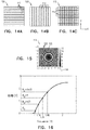
図5A−5Dは、本発明の1実施形態に基づく、図4A−4Cの装置を使用して形成される網膜像の点像分布関数(PSF)を、異なるレベルの画素寸法変化に対して概略示すグラフである。PSFを計算するために、眼は、17mmの焦点距離、瞳孔寸法4mmの完全なレンズであると仮定され、一方レンズ66は平均画素ピッチ10μmそして焦点距離1mのフレネルレンズとして動作するように駆動される。眼の光軸はレンズ66の中心に対して5mm偏移していると仮定され、それは回折効果を増大させる。
5A-5D are schematics of point spread function (PSF) of retinal images formed using the apparatus of FIGS. 4A-4C, for different levels of pixel dimensional change, according to one embodiment of the present invention FIG. To calculate PSF, the eye is assumed to be a 17 mm focal length, 4 mm full lens pupil diameter, while
それぞれの図5A−5Dは、上記で定義された方式における、ミクロンで表された異なる電極幅の標準偏差σにおける、回折次数に対する振幅を示す。図5A−5Dは、高い回折次数を強調するようにスケーリングされ、図面では見られないゼロ次のピーク値は、0.02である。図5Aに示すように、10%の標準偏差を意味するσ=1ミクロンに対しては、1次回折次数はゼロ次の0.3%未満に減少し、したがって、見えるとしてもかろうじて知覚できる。高い標準偏差については、1次回折次元は、さらに減少している。標準偏差の増加に伴って総散乱光が低減されず、そしてわずかに増加さえしているが、しかしこの散乱は、被験者の視力を妨げない。 Each of FIGS. 5A-5D shows the amplitude with respect to the diffraction order, in standard deviation σ of different electrode widths expressed in microns, in the manner defined above. 5A-5D are scaled to emphasize high diffraction orders, the zero order peak value not seen in the drawing is 0.02. As shown in FIG. 5A, for σ = 1 micron, which means a standard deviation of 10%, the first diffraction order is reduced to less than 0.3% of the zero order, and thus can be perceived barely, if visible. For high standard deviations, the first order diffraction dimension is further reduced. Although total scattered light is not reduced and may even increase slightly with increasing standard deviation, this scattering does not interfere with the subject's vision.
図6A−6Cは、本発明の代替的な実施形態による、電気的に調整可能なレンズ76を概略示す図である。図6Aと6Bはレンズ76の反対の両側70と72に形成された電極74の正面図である。図6Cはレンズ76の正面図であり、レンズの反対の両側の電極74の重ね合わせを示す。70の側の水平電極と72の側の垂直電極との交点は画素78の配列を画定する。
6A-6C schematically illustrate an electrically
図6A及び図6Bに見ることができるように、電極74の幅は、互いに異なるだけでなく、電極の軸に沿って変化している。(電極74の軸は、電極の長手方向に沿った重心軸であるように設定され、それらは小さな偏差で平行である。)したがって、画素78の大きさと形状の両方がレンズ76の領域にわたって変化し、そして回折効果は無視できる。説明を明確にするために、図6C中の寸法変化は非常に大きいが、実際の実施では変化は、所望の位相変調プロファイルの正確な生成を可能にするために一般的にはより小さい。代替的には、電極74の幅の変化は、本図に示すようにランダムな振幅を有する周期的なものであるよりはむしろ、滑らかであってもよい。
As can be seen in FIGS. 6A and 6B, the widths of the
図7A−7Cは、本発明の代替的な実施形態による、電気的に調整可能なレンズ77を概略示す図である。図7Aと7Bはレンズ77の反対の両側71と73に形成された電極75の正面図である。図7Cはレンズ77の正面図であり、レンズの反対の両側の電極75の重ね合わせを示す。71の側の水平電極と73の側の垂直電極との交点は画素79の配列を画定する。
7A-7C schematically illustrate an electrically
図7A及び図7Bに見ることができるように、電極75の幅はほぼ一定であるが、その中心点は、電極のそれぞれの軸に沿って変化する量だけ横方向にずれていて、電極の軸はここでもまた電極の長手方向に沿って重心軸に設定されている。この例では、全ての電極の軸に沿って測定された側面71又は73の端部からの横方向の偏移が一定であり、それにより一定の電極幅が維持され、しかし代替的には、任意の電極の幅と偏移は変化してもよい。電極の変化する横方向偏移は、空間フーリエ変換において画素79のピッチに対応する変化をもたらし、それにより、そうでなければ生成される回折ピークとゴースト画像を軽減する。
As can be seen in FIGS. 7A and 7B, the width of the
図6A−6Cおよび図7A−7Cは、電極74又は75の配列が両側でクロスして延在するレンズ76と77を示しているが、これらの実施形態の原理は、同様に、不均一な幅および/または偏移を持つ電極が電気光学層の片面のみに伸長している円筒レンズで実施することができる。互いに直交する2つのレンズの電極軸を有する、このような円柱レンズの1組は、レンズ74または75と実質的に同一の集束効果を達成するために使用することができる。
6A-6C and 7A-
電極間の領域の滑らかさを維持するために、制御回路38によって印加される隣接する電極を駆動するための波形は、一般的に同じ極性でなければならない。この規則の例外は、フレネルレンズにおけるように、位相変調プロファイルの急激な転移が存在する場合に発生する。この場合、制御回路は、位相変調プロファイルの急峻な変化を達成するために、急激な相転移の近くにある相互に隣接する励起電極の組に対し、反対の極性のそれぞれの制御電圧波形を印加してもよい。
In order to maintain the smoothness of the area between the electrodes, the waveforms for driving adjacent electrodes applied by
追加的または代替的に、電気光学層の位相変調プロファイルの急激な転移は、転移の両側にある電極を、所定の位相変調振幅に対する公称電圧をオーバーシュートまたはアンダーシュートする電圧で駆動することによって鮮鋭化することができる。しかしながら、上述のように、幅広の電極が使用される場合、電気光学層内の対応する幅広の領域にわたるオーバーシュート及びアンダーシュートは、レンズの集光品質に負の影響を与える可能性がある。この問題は、以下の図に示すように、異なる、それぞれの幅を有する電極を使用することによって対処することができる。これらの実施形態の特徴は、上記の実施形態のものと組み合わせることができ、そして電気光学層の一方の側に励起電極の単一の配列を有するか、反対の両側に互いに垂直に配置される2つの配列を有するか、のいずれかの装置で実施されてもよい。 Additionally or alternatively, a rapid transition phase modulation profile of the electro-optic layer, sharpening an electrode on each side of the transition, by driving a voltage to overshoot or undershoot the nominal voltage for a given phase modulation amplitude Can be However, as described above, if the wide electrodes are used, overshoot and undershoot over the corresponding wide area of the electro-optic layer is likely to have a negative effect on the condensing lens quality. This problem can be addressed by using electrodes with different respective widths, as shown in the following figures. The features of these embodiments can be combined with those of the above embodiments and have a single array of excitation electrodes on one side of the electro-optic layer or be arranged perpendicular to each other on opposite sides It may be implemented in any of the two- arrangement arrangements .
図8は、本発明のこのような1つの実施形態による、電気的に調整可能なレンズ80の電極82、84の概略正面図である。レンズ80の設計は、狭い電極84がメイン変調電極82の中に散在する。狭い電極84の幅は、一般的にメイン変調電極82の半分以下の幅であり、更にそれ以下であってもよい。実際には、狭い電極84の幅は、電極間のギャップ幅4倍より大きくなく、または可能性としてギャップ幅と等しいかそれ以下でもよい。この電極の幅は、電気光学層自体の厚さより小さくてもよい。
FIG. 8 is a schematic front view of the
制御回路によって印加される制御電圧波形は、位相変調プロファイルの急激な転移が狭い電極84の近傍で発生するように調整される。狭い電極はこれら転移を鮮鋭にするため、必要に応じてオーバーシュートまたはアンダーシュート電圧で駆動される。しかし狭いストライプ幅のため、オーバーシュートまたはアンダーシュートが、相転移境界における狭い空間帯域に制限され、一方メイン変調電極82により生成された位相変調プロファイルの残りの部分は滑らかで良く形成されている。
The control voltage waveform applied by the control circuit is adjusted such that abrupt transitions of the phase modulation profile occur in the vicinity of the
本発明のいくつかの実施形態では、このようなフレネルレンズのような急激な相転移を有する位相変調関数が図8に示すような構造で実装される場合、電気光学層によってサポートされる位相変調値の範囲は、位相変調関数における急激な転移の間の間隔に対する、狭い電極84の密度との比率に比例して増加する。狭い電極の密度が高いと、位相変調値の必要な範囲の増加がより小さくなる。例えば、2πの急激な相転移を有する、離間距離Xだけ離れているフレネルプリズムは、X離間している電極構造が2πから0への急激な転移をサポートする限り、0から2πの位相変調値をサポートする電気光学層を用いて実施することができる。しかしながら、急激な転移が狭い電極84の位置に限定され、そして、狭い電極の位置と位相変調関数の急激な転移の場所との間の完全な重なりはない、実際のケースでは、電気光学層は2πよりも大きい変調範囲をサポートする必要がある。例えば、狭い電極の間の距離が0.3Xである場合、狭い電極の位置にマッチするため、いくつかの急激な転移は1.2Xだけ離間されなければならない(そして他の場所では0.9Xだけ離間)。このような場合には、電気光学層の位相変調範囲は、20%大きく、0から2.4πの範囲をカバーしなければならない。狭い電極が2X離れている場合は、急激な転移もまた2X離れ、そして活性層は0から4πの位相変調範囲をサポートする必要がある。
In some embodiments of the present invention, the phase modulation supported by the electro-optical layer if the phase modulation function having such a rapid phase transition such as a Fresnel lens is implemented with a structure as shown in FIG. The range of values increases in proportion to the ratio of the
図9は、本発明の代替的な実施形態による、電気的に調整可能なレンズ86における電極82、84の概略正面図である。この実施形態は、図8のものと同様だが、レンズ86の狭い電極84は、印加される波形および位相変調分布のより正確な局所的制御を可能にするために対にされる。この場合、1対の狭い電極の一方は、過大電圧で駆動され、他の一方は過小電圧で駆動されてもよい。
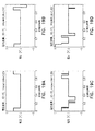
FIG. 9 is a schematic front view of
図10は、本発明の実施形態による、2つの電気的に調整可能なレンズにおける位相変調の変化を示すグラフである。実線の曲線90は、均一な幅の電極を有するレンズの位相変調プロファイルにおける2πの転移を示し、一方破線の曲線92は、図8の装置のように、狭い電極84を用いて達成されるシャープな転移を示す。両方の場合の電極間のギャップはg=2μm、そして電極84は幅2μmである。電極は、振幅3.3Vのパルス幅変調(PWM)信号で駆動される。図10の左側の低位相電極は、5%のデューティサイクル(Vrms=0.74V)を有し、図の右側の高位相電極は、20%のデューティサイクル(Vrms=1.47 V)を有する。曲線92を生成するために、転移の高い側の電極84は26%のデューティサイクル(Vrms=1.68V)で、オーバーシュート電圧で駆動される。位相変調関数の2π転移は、このように電圧オーバーシュートと狭い電極84を使用する場合に、目に見えてより急峻である。
FIG. 10 is a graph showing the change in phase modulation in two electrically tunable lenses according to an embodiment of the present invention. The
(望まない位相変化を避ける)
前の図2Aおよび図2Bに示すように、画素化された電気的に調整可能なレンズの最も基本的なパラメータはピッチpであり、それは変調関数の空間的なサンプリングレートを決定する。ピッチは、位相変調関数が画素間で有意に変化しないことを保証するのに十分なほど小さくなければならない。
(Avoid unwanted phase changes)
As shown in the previous FIGS. 2A and 2B, the most basic parameter of a pixilated electrically adjustable lens is the pitch p, which determines the spatial sampling rate of the modulation function. The pitch should be small enough to ensure that the phase modulation function does not change significantly between pixels.
電極間のギャップ幅gは、滑らかで連続的な変調関数を達成するためにまた重要であり、そして電気光学層の厚さdよりもはるかに大きくてはいけない。もしg>>dの場合、電極間のギャップの下の電気光学材料に印加される電界は、電極の下方に印加される電界よりも有意に小さく、その結果光変調関数の有意の不連続を生じる。したがって、ギャップ幅gは、電気光学層の厚さdより小さく、そして可能で配列ば電気光学層の厚さの半分未満であることが望ましい。 The gap width g between the electrodes is also important to achieve a smooth and continuous modulation function, and should not be much larger than the thickness d of the electro-optic layer. If g >> d, the electric field applied to the electro-optic material below the gap between the electrodes is significantly smaller than the electric field applied below the electrodes, resulting in significant discontinuities in the light modulation function It occurs. Thus, it is desirable for the gap width g to be less than the thickness d of the electro-optic layer, and possibly less than half the thickness of the electro-optic layer if aligned .
図11は、本発明の実施形態による、電極間の異なるギャップ幅における、電気的に調整可能なレンズの隣接する電極間の位相変調の変化を示すグラフである。必要な位相変調は4.7ラジアンで一定であるので、ギャップの両側の2つの電極に同一の電圧が印加される。液晶層の厚さはd=5μmとする。曲線93、94と95は、それぞれギャップ幅g=10μm、g=5μm、g=2μmの場合の電極間のギャップに隣接する液晶内の位相変化を示す。
FIG. 11 is a graph showing the change in phase modulation between adjacent electrodes of an electrically tunable lens at different gap widths between electrodes according to an embodiment of the present invention. Since the required phase modulation is constant at 4.7 radians, the same voltage is applied to the two electrodes on either side of the gap. The thickness of the liquid crystal layer is d = 5 μm.
曲線93、94と95は、滑らかで連続的な位相変調関数が必要とされる場合、小さなギャップ幅を有することの利点を明確に示す。電気光学層の厚さよりも大きいギャップ幅の曲線93においては、位相変調は電極間で必要な4.7から0.9ラジアンに低下する。電気光学層の厚さに等しいギャップ幅の曲線94では、位相変調の低下は、それより極端でなく、一方ギャップ幅が電気光学層の厚みの半分未満の曲線95では、位相変調は4.5ラジアンまでしか低下しない。従って、所定の製造上の制約(例えば、フォトリソグラフィ工程のフィーチャサイズのような)の下で達成可能な最小のギャップを使用することが殆どの場合に有益である。
図12は、本発明の代替的な実施形態による、レンズ内に電極44の間のバッファ層98と電気光学層48を備える電気的に調整可能なレンズ96の概略断面図である。バッファ層98は、ガラス又は適切なポリマー等の透明な絶縁体材料からなり、典型的には少なくとも0.2μm、ほとんどの場合少なくとも0.5μmの厚さを有し、それは電気光学層から励起電極を分離する。バッファ層98の内側表面は、電気光学層48の一つの面に隣接し、一方基板40上の電極44は、バッファ層の外側表面を横断して伸長する。図示の実施形態では、基板42上の共通電極46が、電気光学層48の活性領域を横断して伸長する。しかし基板42上にも電極パターンが存在する場合は、バッファ層98と同様に、追加のバッファ層(図示せず)を底部基板の頂部に配置することができる。
FIG. 12 is a schematic cross-sectional view of an electrically
電気光学層48中の電界が電極44間のギャップにより最も影響され、図11に示す望ましくない位相変調の変化をもたらす領域は、ギャップに隣接しバッファ層の近くの領域である。バッファ層98はこれらの領域から電気光学層48の電気光学材料を遠ざけ、そしてこの目的のため、バッファ層98はギャップ幅の少なくとも4分の1の厚さを有するべきである。それにより、電気光学材料は、より滑らかな電場を経験し、そして位相変調はより滑らかである。
The area in the electro-
図13は、本発明の実施形態によるレンズ96内と、バッファ層なしの同等のレンズ内の、画素間の位相変調の変化を示すグラフである。この事例では、電気光学層48の厚さは、d=5μmであり、一方電極44は、幅w=9μmを有し、そしてギャップ幅g=3μmのギャップによって分離されている。曲線100は、バッファ層なしの電気光学層48内の位相変化を示し、一方、曲線102は、厚さb=1μmのバッファ層98を加えた位相変化を示す。バッファ層は、光変調関数を平滑化し、そしてより連続的な変調を達成する。
FIG. 13 is a graph showing the change in phase modulation between pixels in a
他方でバッファ層は、フレネル型プロファイルにおける2nπの急激な相転移を滑らかにし、従って、これらの領域での変調エラーを増大させる。これらのエラーは電気光学層48に直接隣接しているバッファ層98の側(図12では下側)に追加の狭い電極を配置することによって減少させることができる。後者のこれらの電極は、図7−9を参照して上述したようなやり方で、急激な変調の変化を実行する際に使用することができる。
The buffer layer, on the other hand, smooths the 2nπ abrupt phase transitions in the Fresnel-type profile and thus increases the modulation error in these regions. These errors can be reduced by placing an additional narrow electrode on the side (lower side in FIG. 12) of the
(分離型変調関数のための駆動波形)
図14A−14Cは、本発明の実施形態による、X方向及びY方向に分離可能な位相変調プロファイルを生成する際に使用される、電気的に調整可能なレンズ112を概略示す図である。図14Aおよび14Bは、レンズ112の電気光学媒体(これらの図には示されていない)のそれぞれ反対の側面106および108に形成された電極110の概略正面図である。図14Cは、レンズ112の概略正面図であり、装置の反対の両側の電極110の重ね合わせによって画定される画素114の行列を示す。
(Drive waveform for separable modulation function)
14A-14C schematically illustrate electrically
先に述べたように、レンズ112は、駆動されて位相変調プロファイル
例えば、以下の表Iは4つの位相変調レベル、θk=kπ/2、k=0,1,2,3への量子化を前提とした、1つの画素を画定する垂直および水平電極に印加された、電圧波形の関数としての当該画素の位相変調を示す:
本発明のもう1つの実施形態では、電圧波形Vx、k(t)およびVy、k(t)は、位相変調のダイナミックレンジを減少させることにより、より効果的な変調を可能にする方法で定義される。詳細には、電圧波形Vx、k(t)およびVy、k(t)は、任意の(k1、k2)に対し、垂直電極にVx、k1(t)を、水平電極にVy、k2(t)を印加することが次式の位相変調をもたらす、ように定義される:
このアプローチの結果として、より薄い電気光学層が使用でき、急激な変化が必要な場合、より険しい相転移が可能になる。あるいは、この種のアプローチは変調関数において位相の不連続の数を減らすために使用できる。 As a result of this approach, thinner electro-optic layers can be used and more abrupt phase transitions are possible if abrupt changes are required. Alternatively, this type of approach can be used to reduce the number of phase discontinuities in the modulation function.
以下の表IIは4つの量子化レベル(表Iと同じ)に対するアプローチを示し、ここでn=1であり、即ち:
電圧波形が表IIによって定義される場合、電気光学層は表Iの場合の3πと比較して、3π/2の動的位相変調レンジをサポートすることが必要であり、これにより、より薄い活性層が可能となり、そして位相不連続が必要とされる場合により急激な転移が可能となる。 If the voltage waveform is defined by the table II, the electro-optical layer as compared to 3 [pi] in the case of Table I, it is necessary to support dynamic phase modulation range of 3 [pi] / 2, thereby, a thinner active Layers are possible, and more abrupt transitions are possible if phase discontinuities are required.
あるいは、所定の電気光学層の厚さに対して、位相の不連続の数を減らすために上記のアプローチを使用することができる。この場合、駆動方式は、表IIに示したものと同様であるが、しかしそれぞれの軸は0から4πまでの範囲の値(表IIの2πの限界の代わりに)で変調され、そして垂直方向と水平方向の電極上の位相和は法4π(表IIの2πでなく)である。表Iの方式を使用する場合、電気光学層が4π以上の動的変調範囲をサポートしている場合でも、位相の不連続性は、X軸またはY軸のいずれかにおいて、必要な変調が2πをまたぐたびに発生する。一方、表IIに示したのと同様の方式を使用し、しかしn=2(法4π)の場合、位相の不連続性は、必要な変調が4πをまたぐたびに円筒対称性をもって発生する。 Alternatively, for a given electro-optic layer thickness, the above approach can be used to reduce the number of phase discontinuities. In this case, the drive scheme is similar to that shown in Table II, but the respective axes are modulated with values ranging from 0 to 4π (instead of the 2π limit of Table II) and in the vertical direction And the phase sum on the horizontal electrodes is modulo 4π (not 2π in Table II). When using the scheme of Table I, even if the electro-optic layer supports a dynamic modulation range of 4π or more, phase discontinuities may require 2π modulation required in either the X or Y axis. It occurs whenever it straddles. On the other hand, using a scheme similar to that shown in Table II, but with n = 2 (Modulus 4π), phase discontinuities occur with cylindrical symmetry with every necessary modulation crossing 4π.
図15は、本発明の実施形態による、上述したように駆動された場合に、レンズ112によって生成される位相変調プロファイル116の概略図である。位相変調プロファイル116は、フレネルレンズをエミュレートし、0から4πまでの位相偏移の振幅スケール118を持つ。プロファイル116は、振幅4πの急激な相転移によって分離された、中心ローブ120と周辺次元122を含む。この方式は、振幅の2π毎の変化での転移を有するフレネルプロファイルに比べて、位相不連続の数を有意に減少させ、従って、位相変調器のなかでこれら急激な転移が占める領域を減少させ、それにより位相変調関数の精度を向上させる。
FIG. 15 is a schematic diagram of the
図16は、本発明の実施形態による、レンズ112内の電極110に印加される電圧の関数としての位相変調曲線を示すグラフである。図16に示すように、θ0、θ0+π/2、θ0+πおよびθ0+3π/2の位相変調が、それぞれ1.02V、1.14V、1.29Vおよび1.46Vの平均二乗平方根(RMS)電圧を、画素を横断して印加することにより得られる。
FIG. 16 is a graph showing a phase modulation curve as a function of voltage applied to
図17A−17D及び図18A−18Dは、本発明の実施形態による、この種のデューティサイクル変調方式において電極110に印加される成分電圧波形を概略示すグラフである。図17A−17Dは、レンズ112の側面106上のX電極に印加される、異なるデューティサイクルの4つの異なる波形を示し、一方図18A−18Dは、側面108上のY電極に印加される、同様に異なるデューティサイクルの、電圧波形を示す。この例における電圧波形は、3つの値:0および±2.5Vに制限され、そして表IIの変調方式に必要なθ0、θ0+π/2、θ0+πおよびθ0+3π/2の位相変調を提供する。代替的に、波形と変調方式の他の組み合わせが、同一またはより多い数の量子化レベルで構成することができる。例えば、各電極が各時間スロットで4つ以上の電圧値の1つを受け取ることができる、アナログ駆動を使用することができる。
17A-17D and 18A-18D are graphs schematically illustrating component voltage waveforms applied to
図17A−17D及び18A−18Dに示された事例では、電気光学層に印加される電圧は、電気光学媒体の応答時間より大きい周波数(例えば、液晶媒体に対しては、100ヘルツより大きい)の交番極性(AC)である。図17A−17Dおよび図18A−18Dに示される波形は、半周期である。実際には、これら波形は、電気光学層の応答が印加電圧のRMS値にのみ依存するように、十分に大きな速度の交番極性で複製される。 In the cases shown in FIGS. 17A-17D and 18A-18D, the voltage applied to the electro-optic layer is of a frequency (eg, greater than 100 Hertz for liquid crystal media) greater than the response time of the electro-optic medium. It is alternating polarity (AC). The waveforms shown in FIGS. 17A-17D and 18A-18D are half periods. In practice, these waveforms are replicated at a sufficiently high rate of alternating polarity so that the response of the electro-optic layer depends only on the RMS value of the applied voltage.
図19A−19Gは、図17A−17Dおよび図18A−18Dの波形の異なる組み合わせを、レンズの反対の両側106と108の上の電極110に印加した結果として、レンズ112の電気光学層を横断して生成される電圧波形を概略示すグラフである。簡潔かつ単純にするために、16の組み合わせ波形の一部のみが示されている。グラフのタイトルは、波形の平均二乗平方根(RMS)電圧値を含み、それは図16に示すRMS値と一致し、そして表IIの位相偏移値に対応する。
19A-19G cross the electro-optic layer of
この例のX電極とY電極の間の電圧差は、0、±2.5V、及び±5Vに制限されている。多くの数の電圧値の使用は波形にさらに自由度を加え、それは幾つかの波形に出現する短いパルスを除去するために使用できる。 The voltage differences between the X and Y electrodes in this example are limited to 0, ± 2.5V, and ± 5V. The use of a large number of voltage values adds more freedom to the waveform, which can be used to eliminate short pulses that appear in some waveforms.
(電気的に調整可能な直列円筒レンズ)
図20は、本発明の別の実施形態による光学システム130の概略側面図である。前述したように、光学システム130は、直列に配置された、互いに直交する円柱軸を持つ、2つの電気的に調整可能な円筒レンズ132及び134を含む。(例えば、レンズ132の円筒軸は図の紙面の中で垂直方向であって、レンズ134の円筒軸は紙面の中に向かう方向であってよい。)このように、レンズ132及び134は、2次元の変調プロファイルを有する球面または非球面レンズをエミュレートするために、レンズ132及び134のそれぞれの変調プロファイルの重ね合わせとして、一緒に制御することができる。
(Electrically adjustable series cylindrical lens)
FIG. 20 is a schematic side view of an
製造を容易にするためには、レンズ132及び134は、例えば図2Aと2Bに示すように、同一の構造を有することが好都合である。電気光学層48が、偏光依存性液晶のような偏光依存性媒体を含むと仮定すると、レンズ132及び134の偏光軸は、互いに垂直である。その結果、補正が存在しない場合に、レンズ132及び134は、異なる偏光で動作する(従って、二次元レンズとしては効果がないであろう)。この制限を克服するために、システム130は、四分の一波長板などの偏光回転子136を備える。したがってシステム130に入射する光が、レンズ132の偏光軸と整列して垂直偏光であると仮定すると、偏光回転子136は90°だけ偏光軸を回転させ、それによりその光がレンズ134に入射する時に光の偏光軸はレンズ134の偏光軸と整列する。
For ease of manufacture, it is convenient for
明確化のため、上記の説明および対応する図は、電気的に調整可能なレンズのさまざまな異なる特徴に別々に関連するが、これらの特徴は、決して相互に排他的であると考えるべきではない。逆に、当業者は上記説明を読んだ後に、これらの特徴が装置性能の更なる向上を達成するために組み合わせることができることを理解しよう。したがって、上述の実施形態は例として引用され、そして本発明は本明細書に特に示され上述されたものに限定されない、ことを理解されたい。むしろ、本発明の範囲は、先行技術に開示されていない、本明細書に記載された様々な特徴の組合せ及びサブ組み合わせ、ならびに前述の説明を読めば当業者に想起されるそれらの変形および修飾の両方を含む。 For the sake of clarity, the above description and the corresponding figures relate separately to the various different features of the electrically adjustable lens, but these features should in no way be considered mutually exclusive. . Conversely, those skilled in the art will appreciate that, after reading the above description, these features can be combined to achieve further improvements in device performance. Accordingly, it is to be understood that the above-described embodiments are cited as examples, and the present invention is not limited to what has been particularly shown and described herein. Rather, the scope of the present invention is not to be disclosed in the prior art, combinations and subcombinations of the various features described herein, and variations and modifications thereof which will occur to those skilled in the art upon reading the foregoing description. Including both.
Claims (18)
電気光学層の活性領域内の任意の所与の位置において局所実効屈折率を有する電気光学層と、
前記実効屈折率は,前記所与の位置において、前記電気光学層を横断して印加される電圧波形により決定され、;
前記電気光学層の対向する第1と第2の側面に伸長する導電性電極と、
前記導電性電極は、励起電極の1つの配列であって、それぞれ相互に平行な事前設定の方向の軸に沿って、前記電気光学層の前記第1の側面を横断して伸長し、そして前記平行な軸に垂直な横方向のそれぞれの幅が異なる、少なくとも第1と第2の電極を有する、励起電極の1つの配列を有し;および
それぞれの制御電圧波形を前記励起電極に印加し、そして、前記励起電極に同時にそして独立して印加される前記制御電圧を変調し、それにより前記電気光学層内に特定の位相変調プロファイルを生成するように接続される、制御回路と;
を有し、
前記励起電極の前記それぞれの幅は、全ての前記励起電極の平均幅の少なくとも10%の標準偏差で互いに異なる、
ことを特徴とする光学装置。 An optical device,
An electro-optic layer having a local effective refractive index at any given position within the active region of the electro-optic layer,
The effective refractive index is determined by the voltage waveform applied across the electro-optic layer at the given position;
Conductive electrodes extending on opposing first and second sides of the electro-optic layer;
The conductive electrode is an array of excitation electrodes and extends across the first side of the electro-optic layer along axes of preset directions, each parallel to each other, and Having an array of excitation electrodes having at least a first and a second electrode, each having a different lateral width perpendicular to the parallel axes; and applying respective control voltage waveforms to the excitation electrodes, And a control circuit connected to modulate the control voltage applied simultaneously and independently to the excitation electrode, thereby producing a specific phase modulation profile in the electro-optic layer;
I have a,
The respective widths of the excitation electrodes differ from one another by a standard deviation of at least 10% of the average width of all the excitation electrodes.
An optical device characterized by
前記導電性電極は、前記電気光学層の前記第2の側面を横断し、前記第1の方向と垂直な第2の方向に伸長する、第2の励起電極の第2の配列を有し、そして前記第2の配列は、異なるそれぞれの幅を有する少なくとも第3と第4の電極を有する、
ことを特徴とする請求項1または2に記載の装置。 The array of excitation electrodes comprises a first array of first excitation electrodes extending in a first direction across the first side of the electro-optic layer, and the conductive electrode is A second arrangement of second excitation electrodes extending in a second direction transverse to the second side of the electro-optic layer and perpendicular to the first direction, and the second arrangement comprises , With at least third and fourth electrodes having different respective widths,
Device according to claim 1 or 2 , characterized in that.
そして前記機器は、前記第1と第2の光学装置の間に配置される、光を前記第1の偏光から前記第2の偏光に回転させる、偏光回転子を有する、
ことを特徴とする請求項5に記載の機器。 The first and second optical devices comprise first and second polarization dependent electro-optical layers, respectively, and the first optical device modulates light in a first polarization, while The second optical device is arranged to modulate light at a second polarization different from the first polarization,
And the device comprises a polarization rotator disposed between the first and second optical devices for rotating light from the first polarization to the second polarization,
The device according to claim 5 , characterized in that.
前記電気光学層は、前記急激な転移の間の間隔に対する前記第2の電極の密度の関係に比例する、位相変調関数における位相変調の値の範囲を提供するように構成される、ことを特徴とする請求項7−10のいずれかに記載の装置。 The phase modulation profile has multiple abrupt transitions occurring in the vicinity of a corresponding one of the second electrode, and the electro-optic layer is for the second electrode relative to the spacing between the abrupt transitions. apparatus according to any one of 10 - is proportional to the density of the relationship, according to claim 7, configured to provide a range of values of the phase modulation in the phase modulation function, characterized in that to.
電気光学層の活性領域内の任意の所与の位置において局所実効屈折率を有する電気光学層と、
前記実効屈折率は,前記所与の位置において、前記電気光学層を横断して印加される電圧波形により決定され、前記電気光学層は対向する第1と第2の側面を有し、そして前記第1と第2の側面の間の距離に等しい層厚を有し、;
前記電気光学層の前記第1と第2の側面に伸長する導電性電極と、
前記導電性電極は、励起電極の1つの配列であって、前記配列が透明な導電性物質の平行なストライプを有し、前記ストライプはストライプの間のギャップ幅が2μmより大きくなく、前記電気光学層の前記層厚より小さい、ギャップを有する励起電極の1つの配列を有し、;および
それぞれの制御電圧波形を前記励起電極に印加し、それにより前記電気光学層内に特定の位相変調プロファイルを生成するように接続される、制御回路と;
を有することを特徴とする、光学装置。 An optical device,
An electro-optic layer having a local effective refractive index at any given position within the active region of the electro-optic layer,
The effective refractive index is determined by the voltage waveform applied across the electro-optic layer at the given location, the electro-optic layer having opposing first and second sides, and Having a layer thickness equal to the distance between the first and second sides;
Conductive electrodes extending to the first and second sides of the electro-optic layer;
The conductive electrode is an array of excitation electrodes, the array having parallel stripes of transparent conductive material, the stripes having a gap width between stripes not greater than 2 μm, the electro-optic Having one array of excitation electrodes with a gap smaller than the layer thickness of the layer; and applying respective control voltage waveforms to the excitation electrodes, whereby a specific phase modulation profile in the electro-optical layer is obtained A control circuit connected to generate;
An optical device comprising:
電気光学層を提供するステップと、
前記電気光学層は、電気光学層の活性領域内の任意の所与の位置において局所実効屈折率を有し、
前記実効屈折率は,前記所与の位置において、前記電気光学層を横断して印加される電圧波形により決定され、;
導電性電極を前記電気光学層の対向する第1と第2の側面に配置するステップと、
前記導電性電極は、励起電極の1つの配列であって、前記配列が、前記電気光学層の前記第1の側面を横断して、それぞれの相互に平行な軸に沿った事前設定の方向に伸長し、そして前記平行な軸に垂直な横方向の異なるそれぞれの幅を有する、少なくとも第1と第2の電極を有する励起電極の1つの配列を有し、;および
それぞれの制御電圧波形を前記励起電極に印加し、そして、前記励起電極に同時にそして独立して印加される前記制御電圧を変調し、それにより前記電気光学層内に特定の位相変調プロファイルを生成するために制御回路を接続するステップと;
を有し、
前記励起電極の前記それぞれの幅は、全ての前記励起電極の平均幅の少なくとも10%の標準偏差で互いに異なる、
ことを特徴とする、光学装置を製造する方法。 A method of manufacturing an optical device, said method comprising:
Providing an electro-optic layer;
The electro-optic layer has a local effective refractive index at any given location within the active region of the electro-optic layer,
The effective refractive index is determined by the voltage waveform applied across the electro-optic layer at the given position;
Placing conductive electrodes on opposite first and second sides of the electro-optic layer;
The conductive electrode is an array of excitation electrodes, the array being transverse to the first side of the electro-optic layer and in a preset direction along respective mutually parallel axes An array of excitation electrodes having at least a first and a second electrode, each having a different width in the lateral direction perpendicular to said parallel axis, and; A control circuit is connected for applying to the excitation electrode and modulating the control voltage simultaneously and independently applied to the excitation electrode, thereby generating a specific phase modulation profile in the electro-optical layer Step and;
I have a,
The respective widths of the excitation electrodes differ from one another by a standard deviation of at least 10% of the average width of all the excitation electrodes.
A method of manufacturing an optical device, characterized in that:
前記導電性電極を配置するステップは、前記電気光学層の前記第2の側面を横断し、前記第1の方向と垂直な第2の方向に伸長する第2の励起電極の第2の配列を配置するステップを有し、そして前記第2の配列は異なるそれぞれの幅を有する少なくとも第3と第4の電極を有する、
ことを特徴とする請求項16または17に記載の方法。 The array of excitation electrodes comprises a first array of first excitation electrodes extending in a first direction transverse to the first side of the electro-optic layer, and disposing the conductive electrode And disposing a second array of second excitation electrodes extending in a second direction transverse to the second side of the electro-optic layer and perpendicular to the first direction, and The second arrangement has at least third and fourth electrodes with different respective widths,
A method according to claim 16 or 17 , characterized in that.
Applications Claiming Priority (7)
| Application Number | Priority Date | Filing Date | Title |
|---|---|---|---|
| US201461952226P | 2014-03-13 | 2014-03-13 | |
| US61/952,226 | 2014-03-13 | ||
| US201461969190P | 2014-03-23 | 2014-03-23 | |
| US61/969,190 | 2014-03-23 | ||
| US201461972445P | 2014-03-31 | 2014-03-31 | |
| US61/972,445 | 2014-03-31 | ||
| PCT/IB2015/051766 WO2015136458A1 (en) | 2014-03-13 | 2015-03-11 | Electrically-tunable lenses and lens systems |
Publications (3)
| Publication Number | Publication Date |
|---|---|
| JP2017515139A JP2017515139A (en) | 2017-06-08 |
| JP2017515139A5 JP2017515139A5 (en) | 2018-02-22 |
| JP6515115B2 true JP6515115B2 (en) | 2019-05-15 |
Family
ID=54071016
Family Applications (1)
| Application Number | Title | Priority Date | Filing Date |
|---|---|---|---|
| JP2016555831A Active JP6515115B2 (en) | 2014-03-13 | 2015-03-11 | Electrically adjustable lens and lens system |
Country Status (6)
| Country | Link |
|---|---|
| EP (2) | EP3117266B1 (en) |
| JP (1) | JP6515115B2 (en) |
| CN (1) | CN106104368B (en) |
| AU (2) | AU2015228442B2 (en) |
| CA (1) | CA2939664C (en) |
| WO (1) | WO2015136458A1 (en) |
Families Citing this family (14)
| Publication number | Priority date | Publication date | Assignee | Title |
|---|---|---|---|---|
| AU2015270158B2 (en) | 2014-06-05 | 2017-11-09 | Optica Amuka (A.A.) Ltd. | Control of dynamic lenses |
| ES2904889T3 (en) * | 2016-04-17 | 2022-04-06 | Optica Amuka A A Ltd | Spectacle lens comprising an improved electrically actuated liquid crystal lens |
| US10168586B2 (en) | 2016-08-24 | 2019-01-01 | Liqxtal Technology Inc. | Electrically tunable optical phase modulation element |
| US10551690B2 (en) * | 2017-09-18 | 2020-02-04 | E-Vision Smart Optics, Inc. | Electro-active lens with resistive arcs |
| KR102031076B1 (en) * | 2017-11-29 | 2019-10-11 | (주) 오프렌 | Composite lens containing liquid crystal |
| WO2019135168A1 (en) | 2018-01-08 | 2019-07-11 | Optica Amuka (A.A.) Ltd. | Tunable fresnel lens with improved image quality |
| EP3521868A1 (en) | 2018-01-31 | 2019-08-07 | Essilor International | Phase change optical device |
| US10816858B2 (en) | 2018-10-29 | 2020-10-27 | Liqxtal Technology Inc. | Electrically tunable phase modulation element |
| DE102018221545A1 (en) * | 2018-12-12 | 2020-06-18 | Robert Bosch Gmbh | Projection device |
| EP3757662B1 (en) * | 2019-06-28 | 2022-06-01 | Essilor International | Optical article |
| EP4004642A4 (en) * | 2019-07-25 | 2022-08-31 | Gentex Corporation | Segmented variable controlled electro-optic element |
| KR102299172B1 (en) | 2020-02-11 | 2021-09-06 | 이민호 | Hybrid type lens and glasses for providing varifocal |
| CN112596269A (en) * | 2020-12-18 | 2021-04-02 | 深圳视为光电科技有限公司 | Adjustable liquid lens, optical vision correction glasses and control method thereof |
| CN113655643A (en) * | 2021-08-18 | 2021-11-16 | 中国科学院光电技术研究所 | Array dynamic optical phase correction plate based on electro-optical material |
Family Cites Families (26)
| Publication number | Priority date | Publication date | Assignee | Title |
|---|---|---|---|---|
| JPS62209412A (en) * | 1986-03-10 | 1987-09-14 | Jiesu:Kk | Variable focal length liquid crystal lens for correcting astigmatism |
| JPH05188343A (en) * | 1992-01-09 | 1993-07-30 | Nippon Telegr & Teleph Corp <Ntt> | Light direction control element |
| GB2326263A (en) * | 1997-06-12 | 1998-12-16 | Sharp Kk | Diffractive spatial light modulator and display |
| US6619799B1 (en) * | 1999-07-02 | 2003-09-16 | E-Vision, Llc | Optical lens system with electro-active lens having alterably different focal lengths |
| US7290875B2 (en) * | 2004-11-02 | 2007-11-06 | Blum Ronald D | Electro-active spectacles and method of fabricating same |
| JP4880142B2 (en) * | 2001-09-18 | 2012-02-22 | 株式会社リコー | LIQUID CRYSTAL ELEMENT, LIGHT DEFLECTION ELEMENT, IMAGE DISPLAY DEVICE USING THE LIGHT DEFLECTION ELEMENT, MANUFACTURING METHOD FOR LIGHT DEFLECTION ELEMENT, AND METHOD FOR DRIVING LIGHT DEFLECTION ELEMENT |
| WO2003032066A1 (en) * | 2001-10-05 | 2003-04-17 | E-Vision, Llc | Hybrid electro-active lens |
| GB2383886B (en) * | 2001-12-20 | 2005-07-20 | Corning Inc | Spatial light modulators with improved inter-pixel performance |
| ATE352054T1 (en) | 2003-10-03 | 2007-02-15 | Invisia Ltd | MULTIFOCAL LENS |
| CN101088041A (en) * | 2004-11-02 | 2007-12-12 | E-视觉有限公司 | Electro-active spectacles and method of fabricating same |
| US20100149444A1 (en) * | 2007-04-17 | 2010-06-17 | Koninklijke Philips Electronics N.V. | Beam-shaping device |
| JP2009080286A (en) * | 2007-09-26 | 2009-04-16 | Citizen Holdings Co Ltd | Optical device |
| EP2310905A4 (en) * | 2008-06-06 | 2013-05-29 | Lensvector Inc | Tunable liquid crystal optical device |
| US8970646B2 (en) * | 2008-07-09 | 2015-03-03 | Ostendo Technologies, Inc. | Image construction based video display system |
| KR101472052B1 (en) * | 2008-07-30 | 2014-12-12 | 삼성디스플레이 주식회사 | Display device |
| JP5396944B2 (en) * | 2008-12-22 | 2014-01-22 | ソニー株式会社 | Lens array element and image display device |
| WO2010102295A1 (en) * | 2009-03-06 | 2010-09-10 | The Curators Of The University Of Missouri | Adaptive lens for vision correction |
| JP5286349B2 (en) * | 2010-12-27 | 2013-09-11 | 株式会社東芝 | Gradient index liquid crystal optical element and image display device |
| JP5699394B2 (en) * | 2011-01-06 | 2015-04-08 | 秋田県 | Liquid crystal cylindrical lens array and display device |
| CN102253563A (en) * | 2011-08-15 | 2011-11-23 | 南京中电熊猫液晶显示科技有限公司 | Electrically driven liquid crystal lens with optimized visual angle and stereoscopic display device thereof |
| JP2013045087A (en) * | 2011-08-26 | 2013-03-04 | Toshiba Corp | Three-dimensional image display apparatus |
| JP5893447B2 (en) * | 2012-03-08 | 2016-03-23 | 株式会社ジャパンディスプレイ | Liquid crystal lens, display device, and electronic device |
| JP5599420B2 (en) * | 2012-03-22 | 2014-10-01 | 株式会社東芝 | Liquid crystal fresnel lens element and image display device |
| JP5677359B2 (en) * | 2012-04-13 | 2015-02-25 | 株式会社東芝 | Liquid crystal optical element and image display device |
| JP5297550B1 (en) * | 2012-07-06 | 2013-09-25 | 株式会社東芝 | Liquid crystal optical element and image display device |
| ES2727498T3 (en) | 2012-09-30 | 2019-10-16 | Optica Amuka A A Ltd | Lenses with power and electrically adjustable alignment |
-
2015
- 2015-03-11 CA CA2939664A patent/CA2939664C/en active Active
- 2015-03-11 EP EP15761611.1A patent/EP3117266B1/en active Active
- 2015-03-11 AU AU2015228442A patent/AU2015228442B2/en active Active
- 2015-03-11 WO PCT/IB2015/051766 patent/WO2015136458A1/en active Application Filing
- 2015-03-11 JP JP2016555831A patent/JP6515115B2/en active Active
- 2015-03-11 CN CN201580013398.5A patent/CN106104368B/en active Active
- 2015-03-11 EP EP20199016.5A patent/EP3779582A1/en active Pending
-
2017
- 2017-12-12 AU AU2017276168A patent/AU2017276168B2/en active Active
Also Published As
| Publication number | Publication date |
|---|---|
| CA2939664C (en) | 2022-04-12 |
| WO2015136458A1 (en) | 2015-09-17 |
| CN106104368B (en) | 2019-10-22 |
| AU2017276168A1 (en) | 2018-01-18 |
| AU2015228442A1 (en) | 2016-08-25 |
| CN106104368A (en) | 2016-11-09 |
| JP2017515139A (en) | 2017-06-08 |
| EP3117266B1 (en) | 2021-02-17 |
| AU2015228442B2 (en) | 2017-10-05 |
| EP3117266A1 (en) | 2017-01-18 |
| EP3779582A1 (en) | 2021-02-17 |
| AU2017276168B2 (en) | 2018-12-20 |
| EP3117266A4 (en) | 2017-08-30 |
| CA2939664A1 (en) | 2015-09-17 |
| WO2015136458A4 (en) | 2015-11-12 |
Similar Documents
| Publication | Publication Date | Title |
|---|---|---|
| JP6515115B2 (en) | Electrically adjustable lens and lens system | |
| US20230375884A1 (en) | Electrically-tunable lenses and lens systems | |
| JP6948721B2 (en) | Lens with electrically adjustable output and alignment | |
| JP2017515139A5 (en) | ||
| JP2015533226A5 (en) | ||
| US11747708B2 (en) | Polarization-insensitive phase modulator | |
| US11327385B2 (en) | Polarization-insensitive phase modulator | |
| JP7379262B2 (en) | Liquid crystal alignment member for spatial light phase modulation, spatial light modulation element, and stereoscopic display device | |
| US11340492B1 (en) | Liquid crystal gradient-index lens structure with improved transition region |
Legal Events
| Date | Code | Title | Description |
|---|---|---|---|
| A521 | Request for written amendment filed |
Free format text: JAPANESE INTERMEDIATE CODE: A523 Effective date: 20180110 |
|
| A621 | Written request for application examination |
Free format text: JAPANESE INTERMEDIATE CODE: A621 Effective date: 20180110 |
|
| A977 | Report on retrieval |
Free format text: JAPANESE INTERMEDIATE CODE: A971007 Effective date: 20180928 |
|
| A131 | Notification of reasons for refusal |
Free format text: JAPANESE INTERMEDIATE CODE: A131 Effective date: 20181031 |
|
| A521 | Request for written amendment filed |
Free format text: JAPANESE INTERMEDIATE CODE: A523 Effective date: 20190109 |
|
| TRDD | Decision of grant or rejection written | ||
| A01 | Written decision to grant a patent or to grant a registration (utility model) |
Free format text: JAPANESE INTERMEDIATE CODE: A01 Effective date: 20190403 |
|
| A61 | First payment of annual fees (during grant procedure) |
Free format text: JAPANESE INTERMEDIATE CODE: A61 Effective date: 20190415 |
|
| R150 | Certificate of patent or registration of utility model |
Ref document number: 6515115 Country of ref document: JP Free format text: JAPANESE INTERMEDIATE CODE: R150 |
|
| R250 | Receipt of annual fees |
Free format text: JAPANESE INTERMEDIATE CODE: R250 |
|
| R250 | Receipt of annual fees |
Free format text: JAPANESE INTERMEDIATE CODE: R250 |
|
| R250 | Receipt of annual fees |
Free format text: JAPANESE INTERMEDIATE CODE: R250 |