JP5396944B2 - Lens array element and image display device - Google Patents
Lens array element and image display device Download PDFInfo
- Publication number
- JP5396944B2 JP5396944B2 JP2009063276A JP2009063276A JP5396944B2 JP 5396944 B2 JP5396944 B2 JP 5396944B2 JP 2009063276 A JP2009063276 A JP 2009063276A JP 2009063276 A JP2009063276 A JP 2009063276A JP 5396944 B2 JP5396944 B2 JP 5396944B2
- Authority
- JP
- Japan
- Prior art keywords
- lens
- electrode group
- state
- electrode
- liquid crystal
- Prior art date
- Legal status (The legal status is an assumption and is not a legal conclusion. Google has not performed a legal analysis and makes no representation as to the accuracy of the status listed.)
- Expired - Fee Related
Links
Images


Classifications
-
- G—PHYSICS
- G02—OPTICS
- G02F—OPTICAL DEVICES OR ARRANGEMENTS FOR THE CONTROL OF LIGHT BY MODIFICATION OF THE OPTICAL PROPERTIES OF THE MEDIA OF THE ELEMENTS INVOLVED THEREIN; NON-LINEAR OPTICS; FREQUENCY-CHANGING OF LIGHT; OPTICAL LOGIC ELEMENTS; OPTICAL ANALOGUE/DIGITAL CONVERTERS
- G02F1/00—Devices or arrangements for the control of the intensity, colour, phase, polarisation or direction of light arriving from an independent light source, e.g. switching, gating or modulating; Non-linear optics
- G02F1/01—Devices or arrangements for the control of the intensity, colour, phase, polarisation or direction of light arriving from an independent light source, e.g. switching, gating or modulating; Non-linear optics for the control of the intensity, phase, polarisation or colour
- G02F1/13—Devices or arrangements for the control of the intensity, colour, phase, polarisation or direction of light arriving from an independent light source, e.g. switching, gating or modulating; Non-linear optics for the control of the intensity, phase, polarisation or colour based on liquid crystals, e.g. single liquid crystal display cells
- G02F1/133—Constructional arrangements; Operation of liquid crystal cells; Circuit arrangements
- G02F1/1333—Constructional arrangements; Manufacturing methods
- G02F1/1335—Structural association of cells with optical devices, e.g. polarisers or reflectors
-
- G—PHYSICS
- G02—OPTICS
- G02B—OPTICAL ELEMENTS, SYSTEMS OR APPARATUS
- G02B30/00—Optical systems or apparatus for producing three-dimensional [3D] effects, e.g. stereoscopic images
- G02B30/20—Optical systems or apparatus for producing three-dimensional [3D] effects, e.g. stereoscopic images by providing first and second parallax images to an observer's left and right eyes
- G02B30/26—Optical systems or apparatus for producing three-dimensional [3D] effects, e.g. stereoscopic images by providing first and second parallax images to an observer's left and right eyes of the autostereoscopic type
- G02B30/27—Optical systems or apparatus for producing three-dimensional [3D] effects, e.g. stereoscopic images by providing first and second parallax images to an observer's left and right eyes of the autostereoscopic type involving lenticular arrays
-
- H—ELECTRICITY
- H04—ELECTRIC COMMUNICATION TECHNIQUE
- H04N—PICTORIAL COMMUNICATION, e.g. TELEVISION
- H04N13/00—Stereoscopic video systems; Multi-view video systems; Details thereof
- H04N13/30—Image reproducers
- H04N13/302—Image reproducers for viewing without the aid of special glasses, i.e. using autostereoscopic displays
- H04N13/305—Image reproducers for viewing without the aid of special glasses, i.e. using autostereoscopic displays using lenticular lenses, e.g. arrangements of cylindrical lenses
-
- H—ELECTRICITY
- H04—ELECTRIC COMMUNICATION TECHNIQUE
- H04N—PICTORIAL COMMUNICATION, e.g. TELEVISION
- H04N13/00—Stereoscopic video systems; Multi-view video systems; Details thereof
- H04N13/30—Image reproducers
- H04N13/356—Image reproducers having separate monoscopic and stereoscopic modes
- H04N13/359—Switching between monoscopic and stereoscopic modes
-
- G—PHYSICS
- G02—OPTICS
- G02F—OPTICAL DEVICES OR ARRANGEMENTS FOR THE CONTROL OF LIGHT BY MODIFICATION OF THE OPTICAL PROPERTIES OF THE MEDIA OF THE ELEMENTS INVOLVED THEREIN; NON-LINEAR OPTICS; FREQUENCY-CHANGING OF LIGHT; OPTICAL LOGIC ELEMENTS; OPTICAL ANALOGUE/DIGITAL CONVERTERS
- G02F1/00—Devices or arrangements for the control of the intensity, colour, phase, polarisation or direction of light arriving from an independent light source, e.g. switching, gating or modulating; Non-linear optics
- G02F1/29—Devices or arrangements for the control of the intensity, colour, phase, polarisation or direction of light arriving from an independent light source, e.g. switching, gating or modulating; Non-linear optics for the control of the position or the direction of light beams, i.e. deflection
- G02F1/291—Two-dimensional analogue deflection
Landscapes
- Physics & Mathematics (AREA)
- Engineering & Computer Science (AREA)
- Multimedia (AREA)
- Signal Processing (AREA)
- General Physics & Mathematics (AREA)
- Optics & Photonics (AREA)
- Nonlinear Science (AREA)
- Liquid Crystal (AREA)
- Mathematical Physics (AREA)
- Chemical & Material Sciences (AREA)
- Crystallography & Structural Chemistry (AREA)
- Testing, Inspecting, Measuring Of Stereoscopic Televisions And Televisions (AREA)
Description
本発明は、液晶を用いて電気的にレンズ効果の発生の制御を行うことができるレンズアレイ素子、およびそのレンズアレイ素子を用いて、例えば2次元表示と3次元表示とを電気的に切り替えることができる画像表示装置に関する。 The present invention provides a lens array element capable of electrically controlling the generation of a lens effect using liquid crystal, and electrically switching, for example, two-dimensional display and three-dimensional display using the lens array element. The present invention relates to an image display device capable of
従来より、観察者の両眼に視差のある視差画像を見せることで立体視を実現する2眼式または多眼式の立体表示装置が知られている。また、より自然な立体視を実現する方法として、空間像方式の立体表示装置がある。空間像方式では、放射方向の異なる複数の光線を空間中に放射することで、複数の視野角に対応した空間像を形成する。 2. Description of the Related Art Conventionally, binocular or multi-view stereoscopic display devices that realize stereoscopic viewing by showing parallax images with parallax to both eyes of an observer are known. Further, as a method for realizing a more natural stereoscopic view, there is a spatial image type stereoscopic display device. In the aerial image method, a plurality of light beams having different emission directions are emitted into the space to form an aerial image corresponding to a plurality of viewing angles.
これらの立体表示装置を実現する方法としては、例えば、液晶ディスプレイなどの2次元表示装置と、2次元表示装置からの表示画像光を複数の視野角方向に偏向させる3次元表示用の光学デバイスとを組み合わせたものが知られている。3次元表示用の光学デバイスとしては、例えば、複数のシリンドリカルレンズ(円筒レンズ)を並列配置したレンズアレイが用いられる。例えば2眼式の場合、左右で異なる視差画像を見せることで左右方向に両眼を置いたときに立体感が得られる。これを実現するためには、2次元表示装置の表示面に対して、縦方向に延在するシリンドリカルレンズを横方向に複数並列配置し、2次元表示装置からの表示画像光を左右方向に偏向させ、左右の視差画像が適切に観察者の左右の眼に到達するようにさせれば良い。 As a method for realizing these stereoscopic display devices, for example, a two-dimensional display device such as a liquid crystal display, and an optical device for three-dimensional display that deflects display image light from the two-dimensional display device in a plurality of viewing angle directions; A combination of these is known. As an optical device for three-dimensional display, for example, a lens array in which a plurality of cylindrical lenses (cylindrical lenses) are arranged in parallel is used. For example, in the case of the two-lens type, a stereoscopic effect can be obtained when both eyes are placed in the left-right direction by showing different parallax images on the left and right. In order to realize this, a plurality of cylindrical lenses extending in the vertical direction are arranged in parallel in the horizontal direction with respect to the display surface of the two-dimensional display device, and the display image light from the two-dimensional display device is deflected in the horizontal direction. And the left and right parallax images may appropriately reach the left and right eyes of the observer.
このような3次元表示用の光学デバイスとしては、例えば樹脂成型されたマイクロレンズアレイを用いることができる。また、液晶レンズによる切り替え式のレンズアレイを用いることができる。液晶レンズによる切り替え式のレンズアレイの場合、レンズ効果の有無を電気的に切り替えることができるため、2次元表示装置と組み合わせて、2次元表示モードと3次元表示モードとの2つの表示モードを切り替えることができる。すなわち、2次元表示モードでは、レンズアレイをレンズ効果の無い状態(屈折力の無い状態)とし、2次元表示装置からの表示画像光をそのままの状態で通過させる。3次元表示モードでは、レンズアレイをレンズ効果を発生させた状態(例えば正の屈折力を有する状態)とし、2次元表示装置からの表示画像光を複数の視野角方向に偏向させることで立体視を実現する。 As such an optical device for three-dimensional display, for example, a resin-molded microlens array can be used. A switchable lens array using a liquid crystal lens can be used. In the case of a switchable lens array using a liquid crystal lens, the presence or absence of the lens effect can be electrically switched, so that the two display modes of the two-dimensional display mode and the three-dimensional display mode are switched in combination with the two-dimensional display device. be able to. That is, in the two-dimensional display mode, the lens array has no lens effect (no refractive power), and display image light from the two-dimensional display device is allowed to pass through as it is. In the three-dimensional display mode, the lens array is in a state where a lens effect is generated (for example, a state having a positive refractive power), and the display image light from the two-dimensional display device is deflected in a plurality of viewing angle directions to achieve stereoscopic viewing. To realize.
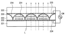
図15および図16は、液晶レンズによる切り替え式のレンズアレイの第1の構成例を示している。このレンズアレイは、例えばガラス材料よりなる透明な第1の基板221および第2の基板222と、それら第1の基板221および第2の基板222の間に挟まれた液晶層223とを備えている。第1の基板221における液晶層223側の表面には、例えばITO(Indium Tin Oxide)膜などの透明な導電膜からなる第1の透明電極224がほぼ全面に一様に形成されている。第2の基板222における液晶層223側の表面にも同様に第2の透明電極225がほぼ全面に一様に形成されている。
15 and 16 show a first configuration example of a switchable lens array using liquid crystal lenses. The lens array includes a transparent
液晶層223は、例えばレプリカ法(Photoreplication Process)と呼ばれる製造方法で、凹レンズ形状に成型された型に液晶分子231が充填された構成となっている。液晶層223における第1の基板221側の面には、配向膜232が平面的に設けられている。液晶層223における第2の基板222側には、レプリカ234の型によって凸形状とされた配向膜233が設けられている。すなわち、液晶層223において、下層の平面的な配向膜232と上層の凸形状の配向膜233との間には液晶分子231が充填され、上層のその他の領域はレプリカ234とされている。これにより、液晶層223では液晶分子231が充填された部分が凸形状とされている。この凸形状の部分が、電圧の印加に応じて選択的にマイクロレンズとなる部分である。
The
液晶分子231は、屈折率異方性を有し、例えば長手方向と短手方向とで通過光線に対して屈折率の異なる屈折率楕円体の構造を有している。また、液晶分子231は、第1の透明電極224と第2の透明電極225とにより与えられる電圧の印加に応じて分子配列が変わるようになっている。ここで、液晶分子231に差電圧として所定の電圧が与えられた状態での分子配列で与えられる、通過光線に対する屈折率をn0とする。また、差電圧がゼロの状態での分子配列で与えられる、通過光線に対する屈折率をneとする。また、屈折率の大きさはne>n0の関係とする。レプリカ34の屈折率は、液晶分子231に差電圧として所定の電圧が与えられた状態での低い方の屈折率n0と同じとなるようにする。
The
これにより、第1の透明電極224と第2の透明電極225とにより与えられる差電圧がゼロの状態では、通過光線Lに対する液晶分子231の屈折率neとレプリカ234の屈折率n0とに屈折率差が生じる。結果、図16に示したように、凸形状の部分が凸レンズとして作用する。一方、差電圧が所定の電圧の状態では、通過光線Lに対する液晶分子231の屈折率n0とレプリカ234での屈折率n0とが同じとなり、凸形状の部分は凸レンズとして作用しなくなる。これにより、図15に示したように、液晶層223を通過する光線は偏向することなく、そのまま透過する。
As a result, when the difference voltage provided by the first
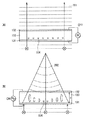
図17(A),(B)、図18および図19は、液晶レンズによる切り替え式のレンズアレイの第2の構成例を示している。このレンズアレイは、図17(A),(B)に示したように、例えばガラス材料よりなる透明な第1の基板101および第2の基板102と、それら第1の基板101および第2の基板102の間に挟まれた液晶層103とを備えている。第1の基板101と第2の基板102は、間隔dを空けて対向配置されている。
FIGS. 17A, 17B, 18 and 19 show a second configuration example of a switchable lens array using liquid crystal lenses. As shown in FIGS. 17A and 17B, the lens array includes a transparent
第1の基板101上における第2の基板102に対向する側には、図18および図19に示したように、ITO膜などの透明な導電膜からなる第1の透明電極111がほぼ全面に一様に形成されている。また、第2の基板102上における第1の基板101に対向する側には、図18および図19に示したように、ITO膜などの透明な導電膜からなる第2の透明電極112が部分的に形成されている。第2の透明電極112は、図19に示したように、例えば幅Lの電極幅を有して例えば縦方向に延在している。そして、第2の透明電極112は、レンズ効果を発生させたときのレンズピッチpに相当する周期間隔で複数、並列的に配置されている。隣り合う2つの第2の透明電極112間は間隔Aの開口とされている。なお、図19では、第2の透明電極112の電極配置を説明するため、第1の基板101を上側に、第2の基板102を下側にして、上下を逆にした状態で図示している。
On the side facing the
なお、図示を省略するが第1の透明電極111と液晶層103との間には配向膜が形成されている。同様に、第2の透明電極112と液晶層103との間には配向膜が形成されている。図17(A)に示したように液晶層103は、図15および図16で示した構成例のようなレンズ状の型はなく、屈折率異方性を有する液晶分子104が一様に分布している。
Although not shown, an alignment film is formed between the first
このレンズアレイでは、図17(A)に示したように、印加電圧が0Vの通常の状態では、液晶分子104が配向膜によって規定される所定の方向に一様に配列される。このため、通過光線の波面201は平面波となり、レンズ効果の無い状態となる。一方、このレンズアレイでは、第2の透明電極112が、図18および図19に示したように間隔Aの開口を有して離間配置されているため、図18に示したような状態で所定の駆動電圧を印加すると、液晶層103内での電界分布に偏りが生ずる。すなわち、第2の透明電極112が形成されている領域に対応する部分では駆動電圧に応じて電界強度が強くなり、間隔Aの開口の中心部に行くほど電界強度が弱くなるような電界が発生する。このため、図17(B)に示したように、液晶分子104の配列が電界強度分布に応じて変化する。これにより、通過光線の波面202が変化し、レンズ効果が発生する状態となる。
In this lens array, as shown in FIG. 17A, in a normal state where the applied voltage is 0 V, the
特許文献1には、図18および図19に示した電極構造における第2の透明電極112の部分を2層構造とした液晶レンズが開示されている。この液晶レンズでは、液晶層の片側に形成する透明電極の配置間隔を第1層目と第2層目とで変えることで、液晶層に形成される電界分布の制御をより最適化しやすくしている。
Patent Document 1 discloses a liquid crystal lens in which the portion of the second
しかしながら、図15および図16に示したレンズアレイを2次元表示モードと3次元表示モードとの切り替えに使用する場合、以下のような問題がある。まず、液晶分子231を充填するための型を基板上に形成させる必要があり、プロセス的にもコスト的にも非常に不利である。また、液晶層223に電圧を印加しない状態でレンズ効果が発生する状態、すなわち3次元表示モードとなるが、現時点では、2次元表示の使用頻度の方が高いことが容易に予想がつくため、消費電力の面で不利と考えられる。また、液晶層223に明確な型があるためか、また、液晶の視野角依存性のためか、2次元表示モードでの画像表示品位が悪いという問題がある。
However, when the lens array shown in FIGS. 15 and 16 is used for switching between the two-dimensional display mode and the three-dimensional display mode, there are the following problems. First, it is necessary to form a mold for filling the
一方、図17(A),(B)に示したレンズアレイを使用する場合、液晶層103に電圧を印加しない状態がレンズ効果が無い状態、すなわち2次元表示モードとなる。このため、2次元表示の使用頻度が高い場合には、消費電力の点では有利である。また、液晶層103にはレンズ状の型はないため、図15および図16に示したレンズアレイに比べて2次元表示モードでの画像表示品位の悪化は少ない。
On the other hand, when the lens array shown in FIGS. 17A and 17B is used, a state where no voltage is applied to the
ところで、通常、据え置き型の表示装置の場合には、画面の縦横方向の表示状態は常に固定されている。例えば画面が横に長い据え置き型の表示装置の場合には、常に横長の表示状態で固定されている。しかしながら、例えば最近の携帯電話機等のモバイル機器では、ディスプレイ部の画面の表示状態を、縦長の状態(画面の縦横比率が縦の方が大きい状態)と、横長の状態(画面の縦横比率が横の方が大きい状態)とに切り替え可能なものが開発されている。このような縦横の表示状態の切り替えは、例えば機器全体、またはディスプレイ部分を表示面内で独立して90°回転させると共に、表示画像も90°回転させることで実現できる。ここで、このような縦横切り替え可能な機器において、3次元表示を行うことを考える。液晶レンズを用いない樹脂成型されたシリンドリカルレンズアレイによって3次元表示を行う方式の場合、通常、2次元表示装置の表示面に対してシリンドリカルレンズアレイは固定されている。このため、縦横のいずれか一方の表示状態でしか正常に3次元表示を行うことができない。例えば横長の表示状態で正常に3次元表示を行えるようにシリンドリカルレンズアレイを配置した場合、縦長の表示状態では、上下方向に屈折力を持つが左右方向には屈折力を持たない状態になるので、正常に立体視を行うことができない。従来の液晶レンズによるシリンドリカルレンズアレイを用いた場合にも、同様の問題が生ずる。すなわち、従来では、液晶レンズを用いて2次元表示モードと3次元表示モードとを切り替えることができるが、3次元表示モードでは縦横の表示状態の切り替えに応じた適切な表示切り替えを行うことができない。 By the way, normally, in the case of a stationary display device, the display state in the vertical and horizontal directions of the screen is always fixed. For example, in the case of a stationary display device having a horizontally long screen, it is always fixed in a horizontally long display state. However, for example, in recent mobile devices such as mobile phones, the display state of the screen of the display unit is in a vertically long state (a state in which the aspect ratio of the screen is larger) and a horizontally long state (the aspect ratio of the screen is horizontal). The one that can be switched to a larger state) has been developed. Such switching between the vertical and horizontal display states can be realized, for example, by rotating the entire device or the display portion by 90 ° independently within the display surface and rotating the display image by 90 °. Here, it is considered that three-dimensional display is performed in such a device capable of switching between vertical and horizontal directions. In the case of a three-dimensional display method using a resin-molded cylindrical lens array that does not use a liquid crystal lens, the cylindrical lens array is usually fixed to the display surface of the two-dimensional display device. For this reason, three-dimensional display can be normally performed only in one of the vertical and horizontal display states. For example, when the cylindrical lens array is arranged so that three-dimensional display can be normally performed in the horizontally long display state, the vertically long display state has a refractive power in the vertical direction but does not have a refractive power in the horizontal direction. Cannot perform stereoscopic viewing normally. A similar problem occurs when a cylindrical lens array using a conventional liquid crystal lens is used. That is, conventionally, it is possible to switch between the two-dimensional display mode and the three-dimensional display mode using a liquid crystal lens, but in the three-dimensional display mode, it is not possible to perform appropriate display switching according to the switching between the vertical and horizontal display states. .
また、特許文献1に記載の液晶レンズのように液晶層の片側を2層の電極構造とする場合には、2層に電極を配置する必要があり、非常にプロセス的にもコスト的にも不利となる。また、デバイス構造としてみると、上下の基板で上の基板側の2層の電極を隔てる誘電体膜分、電気的に非対称構造となっている。この状態を極言すると、上側だけ厚い配向膜を付けたものと同じとなり、液晶の焼付き現象が増長されるなどの問題を引き起こすことが自明である。 In addition, in the case where one side of the liquid crystal layer has a two-layer electrode structure as in the liquid crystal lens described in Patent Document 1, it is necessary to dispose electrodes on the two layers. Disadvantageous. In addition, when viewed as a device structure, a dielectric film component separating two layers of electrodes on the substrate side of the upper and below the substrate, it has an electric asymmetric structure. In short, this state is the same as that with a thick alignment film only on the upper side, and it is obvious that problems such as an increase in the image sticking phenomenon of the liquid crystal are caused.
本発明はかかる問題点に鑑みてなされたもので、その目的は、シリンドリカルレンズ状のレンズ効果を2つの方向に容易に切り替えることができるようにしたレンズアレイ素子、およびそのレンズアレイ素子を用いた画像表示装置を提供することにある。 The present invention has been made in view of such problems, and an object thereof is to use a lens array element that can easily switch the cylindrical lens-like lens effect in two directions, and the lens array element. An object is to provide an image display device.
本発明によるレンズアレイ素子は、間隔を空けて互いに対向配置された第1および第2の基板と、第1の基板上における第2の基板に対向する側に形成され、第1の方向に延在する複数の透明電極が幅方向に間隔を空けて並列配置されてなる第1の電極群と、第2の基板上における第1の基板に対向する側に形成され、第1の方向とは異なる第2の方向に延在する複数の透明電極が幅方向に間隔を空けて並列配置されてなる第2の電極群と、第1の基板と第2の基板との間に配置され、屈折率異方性を有する液晶分子を含み、第1の電極群と第2の電極群とに印加される電圧に応じて液晶分子の配列方向が変化することでレンズ効果が発生する液晶層とを備えている。そして、液晶層が、第1の電極群と第2の電極群とに印加される電圧の状態に応じて、レンズ効果の無い状態と、第1の方向に延在するような第1のシリンドリカルレンズ状のレンズ効果が発生する第1のレンズ状態と、第2の方向に延在するような第2のシリンドリカルレンズ状のレンズ効果が発生する第2のレンズ状態との3つの状態に電気的に切り替わり、かつ、第2の方向は、第1の方向に対して直交する方向であり、直交する第1の方向と第2の方向との2方向にレンズ効果のある状態が電気的に切り替わるようになされているものである。
また、第1の電極群を構成する複数の透明電極は、第1の幅を有して第1の方向に延在する複数の第1の電極と、第1の幅よりも大きい第2の幅を有して第1の方向に延在する複数の第2の電極とからなり、第1の電極群は、それら第1の電極と第2の電極とが交互に並列配置された構成とされ、かつ、第1の電極群における第1の電極は、第1のシリンドリカルレンズのレンズピッチに相当する間隔で配置されている。
第2の電極群を構成する複数の透明電極は、第1の幅を有して第2の方向に延在する複数の第1の電極と、第1の幅よりも大きい第2の幅を有して第2の方向に延在する複数の第2の電極とからなり、第2の電極群は、それら第1の電極と第2の電極とが交互に並列配置された構成とされ、かつ、第2の電極群における第1の電極は、第2のシリンドリカルレンズのレンズピッチに相当する間隔で配置されている。
The lens array element according to the present invention is formed on the first substrate facing the second substrate on the first substrate and the second substrate disposed opposite to each other at an interval, and extends in the first direction. A first electrode group in which a plurality of existing transparent electrodes are arranged in parallel at intervals in the width direction, and formed on a side of the second substrate facing the first substrate, the first direction being A plurality of transparent electrodes extending in different second directions are arranged between a second electrode group in which a plurality of transparent electrodes are arranged in parallel at intervals in the width direction, and the first substrate and the second substrate. A liquid crystal layer that includes liquid crystal molecules having a rate anisotropy and generates a lens effect by changing the alignment direction of the liquid crystal molecules according to a voltage applied to the first electrode group and the second electrode group. I have. Then, the liquid crystal layer has no lens effect according to the state of the voltage applied to the first electrode group and the second electrode group, and the first cylindrical that extends in the first direction. There are three electrical states: a first lens state in which a lens-like lens effect occurs and a second lens state in which a second cylindrical lens-like lens effect that extends in the second direction occurs. switches to, and the second direction is a direction orthogonal to the first direction, the first direction and a state in which a lens effect in the two directions electrically with a second direction perpendicular It is made to switch to.
The plurality of transparent electrodes constituting the first electrode group includes a plurality of first electrodes having a first width and extending in the first direction, and a second larger than the first width. A plurality of second electrodes having a width and extending in the first direction, wherein the first electrode group has a configuration in which the first electrodes and the second electrodes are alternately arranged in parallel; In addition, the first electrodes in the first electrode group are arranged at intervals corresponding to the lens pitch of the first cylindrical lens.
The plurality of transparent electrodes constituting the second electrode group have a plurality of first electrodes having a first width and extending in the second direction, and a second width larger than the first width. And a plurality of second electrodes extending in the second direction, and the second electrode group has a configuration in which the first electrodes and the second electrodes are alternately arranged in parallel. In addition, the first electrodes in the second electrode group are arranged at intervals corresponding to the lens pitch of the second cylindrical lens.
本発明によるレンズアレイ素子では、液晶層が、第1の電極群と第2の電極群とに印加される電圧の状態に応じて、レンズ効果の無い状態と、第1の方向に延在するような第1のシリンドリカルレンズ状のレンズ効果が発生する第1のレンズ状態と、第2の方向に延在するような第2のシリンドリカルレンズ状のレンズ効果が発生する第2のレンズ状態との3つの状態に電気的に切り替わる。例えば、液晶層をレンズ効果の無い状態にする場合には、第1の電極群を構成する複数の透明電極と第2の電極群を構成する複数の透明電極とがすべて同電位となるような電圧状態とする。第1のレンズ状態にする場合には、第2の電極群を構成する複数の透明電極のすべてに共通の電圧を印加すると共に、第1の電極群を構成する複数の透明電極のうち、第1のシリンドリカルレンズのレンズピッチに相当する位置にある透明電極のみに選択的に駆動電圧を印加する。第2のレンズ状態にする場合には、第1の電極群を構成する複数の透明電極のすべてに共通の電圧を印加すると共に、第2の電極群を構成する複数の透明電極のうち、第2のシリンドリカルレンズのレンズピッチに相当する位置にある透明電極のみに選択的に駆動電圧を印加する。 In the lens array element according to the present invention, the liquid crystal layer extends in the first direction and the state without the lens effect according to the state of the voltage applied to the first electrode group and the second electrode group. The first lens state in which the lens effect of the first cylindrical lens is generated, and the second lens state in which the lens effect of the second cylindrical lens is extended in the second direction. Electrically switches between three states. For example, when the liquid crystal layer has no lens effect, the plurality of transparent electrodes constituting the first electrode group and the plurality of transparent electrodes constituting the second electrode group are all at the same potential. Set to voltage state. In the case of the first lens state, a common voltage is applied to all of the plurality of transparent electrodes constituting the second electrode group, and among the plurality of transparent electrodes constituting the first electrode group, A drive voltage is selectively applied only to the transparent electrode located at a position corresponding to the lens pitch of one cylindrical lens. In the second lens state, a common voltage is applied to all of the plurality of transparent electrodes constituting the first electrode group, and among the plurality of transparent electrodes constituting the second electrode group, A drive voltage is selectively applied only to the transparent electrode located at a position corresponding to the lens pitch of the cylindrical lens No. 2.
本発明による画像表示装置は、2次元的に画像表示を行う表示パネルと、表示パネルの表示面側に対向配置され、表示パネルからの光線の通過状態を選択的に変化させるレンズアレイ素子とを備えている。そして、そのレンズアレイ素子を、上記本発明のレンズアレイ素子で構成したものである。 An image display device according to the present invention includes a display panel that displays an image in a two-dimensional manner, and a lens array element that is disposed opposite to the display surface side of the display panel and selectively changes the passage state of light rays from the display panel. I have. The lens array element is constituted by the lens array element of the present invention.
本発明による画像表示装置では、レンズアレイ素子を、レンズ効果の無い状態と、第1のレンズ状態および第2のレンズ状態とに適切に切り替えることにより、例えば2次元表示と3次元表示との電気的な切り替えが可能となる。例えば、レンズアレイ素子をレンズ効果の無い状態として、表示パネルからの表示画像光を偏向させることなく透過させることで2次元表示を行う。また、レンズアレイ素子を第1のレンズ状態として、表示パネルからの表示画像光を第1の方向に直交する方向に偏向させることで、第1の方向に直交する方向に両眼を置いたときに立体感が得られるような3次元表示を行う。また、レンズアレイ素子を第2のレンズ状態として、表示パネルからの表示画像光を第2の方向に直交する方向に偏向させることで、第2の方向に直交する方向に両眼を置いたときに立体感が得られるような3次元表示を行う。 In the image display device according to the present invention, the lens array element is appropriately switched between the state without the lens effect, the first lens state, and the second lens state, for example, the electric power of 2D display and 3D display. Switching is possible. For example, in a state where the lens array element has no lens effect, display image light from the display panel is transmitted without being deflected to perform two-dimensional display. Also, when both eyes are placed in a direction orthogonal to the first direction by deflecting display image light from the display panel in a direction orthogonal to the first direction with the lens array element in the first lens state A three-dimensional display is obtained so that a stereoscopic effect can be obtained. Also, when both eyes are placed in a direction orthogonal to the second direction by deflecting display image light from the display panel in a direction orthogonal to the second direction with the lens array element in the second lens state A three-dimensional display is obtained so that a stereoscopic effect can be obtained.
本発明のレンズアレイ素子によれば、液晶層を挟んで第1の電極群と第2の電極群とを対向配置し、かつ、第1の電極群と第2の電極群とを異なる2方向に延在する複数の透明電極で構成し、それら第1の電極群と第2の電極群とに印加する電圧の状態を適切に制御することで液晶層におけるレンズ効果を適切に制御するようにしたので、レンズ効果の有無を容易に電気的に切り替えることができる。また、シリンドリカルレンズ状のレンズ効果を2つの方向に容易に電気的に切り替えることができる。 According to the lens array element of the present invention, the first electrode group and the second electrode group are arranged to face each other with the liquid crystal layer interposed therebetween, and the first electrode group and the second electrode group are arranged in two different directions. The lens effect in the liquid crystal layer is appropriately controlled by appropriately controlling the state of the voltage applied to the first electrode group and the second electrode group. Therefore, the presence or absence of the lens effect can be easily switched electrically. In addition, the cylindrical lens-like lens effect can be easily switched electrically in two directions.
本発明の画像表示装置によれば、表示パネルからの光線の通過状態を選択的に変化させる光学デバイスとして、本発明のレンズアレイ素子を用いるようにしたので、例えば2次元表示と3次元表示との電気的な切り替えを容易に行うことができる。また、例えば3次元表示を行う場合の表示方向を、異なる2方向に容易に電気的に切り替えることができる。 According to the image display device of the present invention, since the lens array element of the present invention is used as an optical device that selectively changes the state of passage of light from the display panel, for example, two-dimensional display and three-dimensional display Can be easily switched. In addition, for example, the display direction when performing three-dimensional display can be easily electrically switched to two different directions.
以下、本発明の実施の形態について図面を参照して詳細に説明する。 Hereinafter, embodiments of the present invention will be described in detail with reference to the drawings.
<第1の実施の形態>
[レンズアレイ素子および画像表示装置の全体構成]
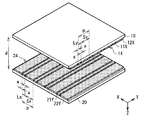
図1は、本発明の第1の実施の形態に係るレンズアレイ素子1の一構成例を示している。このレンズアレイ素子1は、間隔dを空けて互いに対向配置された第1の基板10および第2の基板20と、それら第1の基板10および第2の基板20の間に配置された液晶層3とを備えている。第1の基板10および第2の基板20は、例えばガラス材料または樹脂材料よりなる透明基板である。第1の基板10上における第2の基板20に対向する側には、第1の方向に延在する複数の透明電極が幅方向に間隔を空けて並列配置されてなる第1の電極群14が形成されている。第1の基板10上にはまた、第1の電極群14を介して配向膜13が形成されている。第2の基板20上における第1の基板10に対向する側には、第1の方向とは異なる第2の方向に延在する複数の透明電極が幅方向に間隔を空けて並列配置されてなる第2の電極群24が形成されている。第2の基板20上にはまた、第2の電極群24を介して配向膜23が形成されている。
<First Embodiment>
[Entire configuration of lens array element and image display device]
FIG. 1 shows a configuration example of the lens array element 1 according to the first embodiment of the present invention. The lens array element 1 includes a
このレンズアレイ素子1は、2次元的に画像表示を行う表示パネル2と組み合わされて、例えば、2次元表示モードと3次元表示モードとの2つの表示モードを切り替えることが可能な画像表示装置を構成する。この場合、レンズアレイ素子1は、図1に示したように、表示パネル2の表示面2A側に対向するように配置される。そして、レンズアレイ素子1は、表示モードに応じてレンズ効果を制御することで、表示パネル2からの光線の通過状態を選択的に変化させる。この場合、表示パネル2は、例えば液晶表示ディスプレイで構成することができる。そして、表示パネル2は、2次元表示を行う場合には2次元画像データに基づく映像表示を行い、3次元表示を行う場合には3次元画像データに基づく映像表示を行う。なお、3次元画像データとは、例えば、3次元表示における複数の視野角方向に対応した複数の視差画像を含むデータである。例えば2眼式の3次元表示を行う場合、右眼表示用と左眼表示用の視差画像のデータである。
The lens array element 1 is combined with a
液晶層3は、液晶分子5を含み、第1の電極群14と第2の電極群24とに印加される電圧に応じて液晶分子5の配列方向が変化することでレンズ効果が制御されるようになっている。液晶分子5は、屈折率異方性を有し、例えば長手方向と短手方向とで通過光線に対して屈折率の異なる屈折率楕円体の構造を有している。液晶層3は、第1の電極群14と第2の電極群24とに印加される電圧の状態に応じて、レンズ効果の無い状態と、第1のレンズ状態と、第2のレンズ状態との3つの状態に電気的に切り替わるようになっている。第1のレンズ状態は、第1の方向に延在するような第1のシリンドリカルレンズ状のレンズ効果が発生する状態である。第2のレンズ状態は、第2の方向に延在するような第2のシリンドリカルレンズ状のレンズ効果が発生する状態である。なお、このレンズアレイ素子1において、2つの異なる方向にレンズ効果が切り替わって発生することを除いて、そのレンズ効果発生の基本原理は、図17(A),(B)に示した液晶レンズと同様である。
The
以下、本実施の形態では、上記第1の方向を図1のX方向(紙面の横方向)、上記第2の方向を図1のY方向(紙面に直交する方向)として説明する。X方向とY方向は、基板面内で互いに直交する方向である。 Hereinafter, in the present embodiment, the first direction will be described as the X direction in FIG. 1 (the horizontal direction on the paper surface), and the second direction will be described as the Y direction in FIG. 1 (a direction orthogonal to the paper surface). The X direction and the Y direction are directions orthogonal to each other within the substrate surface.
[レンズアレイ素子1の電極構造]
図2は、このレンズアレイ素子1の電極構造の一構成例を示している。なお、図2では、図19に示した従来の電極構造との違いを分かりやすくするため、第1の基板10を上側に、第2の基板20を下側にして、図1とは上下を逆にした状態で図示している。
[Electrode structure of lens array element 1]
FIG. 2 shows a configuration example of the electrode structure of the lens array element 1. In FIG. 2, in order to easily understand the difference from the conventional electrode structure shown in FIG. 19, the
第1の電極群14は、複数の透明電極として、異なる電極幅を有する2種類の電極を交互に並列配置した構成とされている。すなわち、第1の電極群14は、X方向第1電極(第1の電極11X)と、X方向第2電極(第2の電極12X)とをそれぞれ複数有し、それら第1の電極11Xと第2の電極12Xとが交互に並列配置された構成とされている。第1の電極11Xは、第1の幅Lyを有して第1の方向(X方向)に延在している。第2の電極12Xは、第1の幅Lyよりも大きい第2の幅Syを有して第1の方向に延在している。第1の電極11Xは、レンズ効果として発生する第1のシリンドリカルレンズのレンズピッチpに相当する周期間隔で、複数、並列配置されている。第1の電極11Xと第2の電極12Xは、間隔aの幅を空けて配置されている。
The
第2の電極群24も同様に、複数の透明電極として、異なる電極幅を有する2種類の電極を交互に並列配置した構成とされている。すなわち、第2の電極群24は、Y方向第1電極(第1の電極21Y)と、Y方向第2電極(第2の電極22Y)とをそれぞれ複数有し、それら第1の電極21Yと第2の電極22Yとが交互に並列配置された構成とされている。第1の電極21Yは、第1の幅Lxを有して第2の方向(Y方向)に延在している。第2の電極22Yは、第1の幅Lxよりも大きい第2の幅Sxを有して第2の方向に延在している。第1の電極21Yは、レンズ効果として発生する第2のシリンドリカルレンズのレンズピッチpに相当する周期間隔で、複数、並列配置されている。第2の電極21Yと第2の電極22Yは、間隔aの幅を空けて配置されている。
Similarly, the
[レンズアレイ素子の製造]
このレンズアレイ素子1の製造を行う場合、まず、例えばガラス材料または樹脂材料よりなる第1の基板10および第2の基板20のそれぞれに、例えばITO膜などの透明導電膜を所定のパターンで形成して第1の電極群14および第2の電極群24を形成する。配向膜13,23は、ポリイミド等の高分子化合物を布で一方向に擦るラビング法や、SiO等の斜方蒸着法により形成する。これにより、液晶分子5の長軸を一方向に配向させる。配向膜13,23上には、第1の基板10と第2の基板20との間隔dを一様に保つために、シール材にガラス材料または樹脂材料からなるスペーサ4を分散させたものを印刷する。そして、第1の基板10と第2の基板20とを貼り合わせ、スペーサ入りのシール材を硬化させる。その後に、公知のTN、STN等の液晶材料を、シール材開口部から第1の基板10と第2の基板20との間に注入し、シール材開口部を封止する。そして、液晶組成物を等方相まで加熱してから、徐冷することにより、レンズアレイ素子1を完成させる。なお、本実施の形態においては、液晶分子5の屈折率異方性Δnが大きいほど、より大きいレンズ効果が得られるので、液晶材料をそのような内容組成にすることが好ましい。一方で、屈折率異方性Δnが大きい液晶組成物の場合、却って液晶組成物の物性を損ね、粘性が増加してしまうことによる基体間への注入が困難となったり、低温では結晶に近い状態になったり、内部電界が増大し、液晶素子の駆動電圧が高くなってしまうことがある。このため、製造性とレンズ効果との双方を考慮した内容組成にすることが好ましい。
[Manufacture of lens array elements]
When the lens array element 1 is manufactured, first, a transparent conductive film such as an ITO film is formed in a predetermined pattern on each of the
[レンズアレイ素子の制御動作]
次に、図3および図4(A)〜(C)を参照して、このレンズアレイ素子1の制御動作(レンズ効果の制御動作)を説明する。図3は、レンズアレイ素子1における電圧印加の状態と発生するレンズ効果との対応関係を、電極の接続関係と共に示している。図4(A)〜(C)は、レンズアレイ素子1で発生するレンズ効果を光学的に等価に示している。
[Control operation of lens array element]
Next, a control operation (lens effect control operation) of the lens array element 1 will be described with reference to FIGS. 3 and 4A to 4C. FIG. 3 shows the correspondence between the voltage application state in the lens array element 1 and the generated lens effect, together with the electrode connection. 4A to 4C show the lens effect generated in the lens array element 1 in an optically equivalent manner.
このレンズアレイ素子1では、液晶層3が、第1の電極群14と第2の電極群24とに印加される電圧の状態に応じて、レンズ効果の無い状態と、第1のレンズ状態と、第2のレンズ状態との3つの状態に電気的に切り替わる。第1のレンズ状態は、第1の方向(X方向)に延在するような第1のシリンドリカルレンズ状のレンズ効果が発生する状態である。第2のレンズ状態は、第2の方向(Y方向)に延在するような第2のシリンドリカルレンズ状のレンズ効果が発生する状態である。
In this lens array element 1, the
このレンズアレイ素子1では、液晶層3をレンズ効果の無い状態にする場合には、第1の電極群14を構成する複数の透明電極と第2の電極群24を構成する複数の透明電極とがすべて同電位(0V)となるような電圧状態とする(図3の中央段に示した状態)。この場合、図17(A)に示した場合と同様の原理で、液晶分子5が配向膜13,23によって規定される所定の方向に一様に配列されるので、レンズ効果の無い状態となる。
In the lens array element 1, when the
また、液晶層3を第1のレンズ状態にする場合には、液晶層3を挟む上下の透明電極間で、第1の電極群14の第1の電極11Xに対応する部分において、液晶分子5の配列に変化を生じさせることが可能となるような所定の電位差が生じるようにする。例えば、第2の電極群24を構成する複数の透明電極(第1の電極21Yおよび第2の電極22Y)のすべてに共通の電圧を印加する。かつ、第1の電極群14を構成する複数の透明電極(第1の電極11Xおよび第2の電極12X)のうち第1の電極11Xのみに選択的に所定の駆動電圧を印加する(図3の下段に示した状態)。この場合、図17(B)に示した場合と同様の原理で、液晶層3内での電界分布に偏りが生ずる。すなわち、第1の電極11Xが形成されている領域に対応する部分では駆動電圧に応じて電界強度が強くなり、第1の電極11Xから離れるほど電界強度が弱くなるような電界が発生する。すなわち、第2の方向(Y方向)にレンズ効果が発生するように電界分布が変化する。すなわち、等価的には、図4(B)に示したように、X方向に延在しY方向に屈折力のある第1のシリンドリカルレンズ(X方向シリンドリカルレンズ)31Xが、Y方向に複数、並列配置されたようなレンズ状態となる。この場合には、第1の電極群14のうち、第1のシリンドリカルレンズ31Xのレンズピッチpに相当する位置にある透明電極(第1の電極11X)のみに選択的に電圧が印加されていることになる。
Further, when the
また、液晶層3を第2のレンズ状態にする場合には、液晶層3を挟む上下の透明電極間で、第2の電極群24の第1の電極21Yに対応する部分において、液晶分子5の配列に変化を生じさせることが可能となるような所定の電位差が生じるようにする。例えば、第1の電極群14を構成する複数の透明電極のすべてに共通の電圧を印加する。かつ、第2の電極群24を構成する複数の透明電極のうち第1の電極21Yのみに選択的に所定の駆動電圧を印加する(図3の上段に示した状態)。この場合、図17(B)に示した場合と同様の原理で、液晶層3内での電界分布に偏りが生ずる。すなわち、第1の電極21Yが形成されている領域に対応する部分では駆動電圧に応じて電界強度が強くなり、第1の電極21Yから離れるほど電界強度が弱くなるような電界が発生する。すなわち、第1の方向(X方向)にレンズ効果が発生するように電界分布が変化する。すなわち、等価的には、図4(A)に示したように、Y方向に延在しX方向に屈折力のある第2のシリンドリカルレンズ(Y方向シリンドリカルレンズ)31Yが、X方向に複数、並列配置されたようなレンズ状態となる。この場合には、第2の電極群24のうち、第2のシリンドリカルレンズ31Yのレンズピッチpに相当する位置にある透明電極(第1の電極21Y)のみに選択的に電圧が印加されていることになる。
When the
なお、第1の電極群14と第2の電極群24とで、電極幅(Ly,Lx等)や電極間の間隔aを同じに構成しても良い(Ly=Lx等にする)。この場合、方向が異なるのみでレンズピッチpが同じ、かつ同じ屈折力を持ったシリンドリカルレンズの効果を発生させることができる。逆にいうと、第1の電極群14と第2の電極群24とで、電極幅や電極間の間隔aを異なる構成にすることで、第1のレンズ状態と第2のレンズ状態とで、異なるレンズピッチを有するシリンドリカルレンズの効果を発生させることができる。
The
[画像表示装置の制御動作]
さらに、図5を参照して、このレンズアレイ素子1を用いた画像表示装置の制御動作を説明する。図5は、画像表示装置における表示状態の切り替え例を示している。ここでは、画像表示装置を、例えばモバイル機器のように画面の表示状態を縦長の状態と横長の状態とに切り替え可能なものに適用する場合を例に説明する。かつ、画像表示装置が2次元表示モードと3次元表示モードとに切り替えることができる場合を例に説明する。
[Control operation of image display device]
Furthermore, with reference to FIG. 5, the control operation of the image display apparatus using the lens array element 1 will be described. FIG. 5 shows an example of switching the display state in the image display apparatus. Here, a case will be described as an example where the image display device is applied to an apparatus capable of switching the display state of a screen between a vertically long state and a horizontally long state such as a mobile device. An example in which the image display apparatus can be switched between the two-dimensional display mode and the three-dimensional display mode will be described.
この画像表示装置では、レンズアレイ素子1を、上記したような、レンズ効果の無い状態と、第1のレンズ状態および第2のレンズ状態とに適切に切り替えることにより、2次元表示と3次元表示との電気的な切り替えを行う。例えば、レンズアレイ素子1をレンズ効果の無い状態として、表示パネル2からの表示画像光を偏向させることなく透過させることで2次元表示を行う。図5(C)は画面の表示状態を横長にした状態で2次元表示を行った画面例、図5(D)は縦長にした状態で2次元表示を行った画面例を示している。
In this image display device, two-dimensional display and three-dimensional display are performed by appropriately switching the lens array element 1 between the state having no lens effect, the first lens state, and the second lens state as described above. And electrical switching. For example, two-dimensional display is performed by transmitting the display image light from the
また、レンズアレイ素子1を第1のレンズ状態として、表示パネル2からの表示画像光を第1の方向(X方向)に直交する方向(Y方向)に偏向させることで、第1の方向に直交する方向に両眼を置いたときに立体感が得られるような3次元表示を行う。これは、図5(B)に示したように画面の表示状態を縦長にした状態で3次元表示を行った場合に相当する。この状態では、レンズ効果としては図4(C)に示したような状態(図4(B)の状態を構造的に90°回転させた状態)でレンズ効果が発生しているので、画面の表示状態を縦長にした状態で左右方向に両眼を置いたときに立体感が得られる。
Further, the display image light from the
また、レンズアレイ素子1を第2のレンズ状態として、表示パネル2からの表示画像光を第2の方向(Y方向)に直交する方向(X方向)に偏向させることで、第2の方向に直交する方向に両眼を置いたときに立体感が得られるような3次元表示を行う。これは、図5(A)に示したように画面の表示状態を横長にした状態で3次元表示を行った場合に相当する。この状態では、レンズ効果としては図4(A)に示したような状態でレンズ効果が発生しているので、画面の表示状態を横長にした状態で左右方向に両眼を置いたときに立体感が得られる。
In addition, the lens array element 1 is set to the second lens state, and the display image light from the
以上説明したように、本実施の形態に係るレンズアレイ素子1によれば、第1の電極群14と第2の電極群24とに印加する電圧の状態を適切に制御することで液晶層3におけるレンズ効果を適切に制御するようにした。これにより、レンズ効果の有無を容易に電気的に切り替えることができる。また、シリンドリカルレンズ状のレンズ効果を2つの方向に容易に電気的に切り替えることができる。このレンズアレイ素子1では、液晶層3を挟んで対向する電極の構造が1層の構造となっているので、特許文献1に記載の液晶レンズのように液晶層の片側を2層の電極構造にした場合に比べて、プロセス的にもコスト的にも有利である。さらに、2層の電極構造にした場合のような、液晶の焼付き現象を抑えることができる。
As described above, according to the lens array element 1 according to the present embodiment, the
また、本実施の形態に係る画像表示装置によれば、表示パネル2からの光線の通過状態を選択的に変化させる光学デバイスとして、レンズアレイ素子1を用いるようにしたので、2次元表示と3次元表示との電気的な切り替えを容易に行うことができる。また、3次元表示を行う場合の表示方向を、異なる2方向に容易に電気的に切り替えることができる。
Further, according to the image display apparatus according to the present embodiment, since the lens array element 1 is used as the optical device that selectively changes the passage state of the light beam from the
<第2の実施の形態>
次に、本発明の第2の実施の形態に係るレンズアレイ素子および画像表示装置について説明する。なお、上記第1の実施の形態に係るレンズアレイ素子1および画像表示装置と実質的に同一の構成部分には同一の符号を付し、適宜説明を省略する。
<Second Embodiment>
Next, a lens array element and an image display device according to the second embodiment of the present invention will be described. Note that components that are substantially the same as those of the lens array element 1 and the image display device according to the first embodiment are denoted by the same reference numerals, and description thereof is omitted as appropriate.
上記第1の実施の形態に係るレンズアレイ素子1において、上下の透明電極間での駆動電圧の印加状態を図3に示したような駆動方法で実施した場合、経時的にレンズ形状(液晶分子5の配向状態)が変化し、所望のレンズ状態に制御できなくなるおそれがある。特に、より高精細化させ、かつ応答速度を速くさせる等の目的で、電極間ギャップ(基板間隔d)を狭くした場合、所望のレンズ状態に制御できなくなる可能性が高い。例えば図3の上段に示した状態では、第2の電極群24のうち第1の電極21Yのみを例えば外部駆動回路に接続して選択的に所定の駆動電圧を印加しているが、第2の電極22Yは回路的に切り離され、フローティングした状態となってしまっている。この場合、連続動作させていくと、第2の電極22Yの部分がフローティングしているために、その部分の液晶分子5の配向が初期状況からかけ離れ、制御できていない状況となるおそれがある。図3の上段に示した状態に対して良好なレンズ状態を維持するためには、第2の電極22Yの部分はあたかも電極がないような振る舞いをさせ、かつ回路的にフローティングさせない状況を作り出す必要がある。本実施の形態は、上記第1の実施の形態に係るレンズアレイ素子1に対する駆動方法の改善に関する。レンズアレイ素子および画像表示装置としての基本的な構成は、上記第1の実施の形態と同様であるため、以下、駆動方法に関する部分のみ説明する。
In the lens array element 1 according to the first embodiment described above, when the driving voltage is applied between the upper and lower transparent electrodes by the driving method as shown in FIG. 5 orientation state) may change, making it impossible to control to a desired lens state. In particular, when the gap between the electrodes (substrate distance d) is narrowed for the purpose of higher definition and faster response speed, there is a high possibility that the lens state cannot be controlled to a desired state. For example, in the state shown in the upper part of FIG. 3, only the
図6は、本実施の形態に係るレンズアレイ素子における電圧印加の状態と発生するレンズ効果との対応関係を、電極の接続関係と共に示している。本実施の形態において、第11の電極群14を構成する複数の透明電極(第1の電極11Xおよび第2の電極12X)はそれぞれ、一端が、第1の外部駆動回路としてのX方向信号発生器(第1の駆動信号発生器40X)に接続可能とされている。また、第2の電極群24を構成する複数の透明電極(第1の電極21Yおよび第2の電極22Y)はそれぞれ、一端が、第2の外部駆動回路としてのY方向信号発生器(第2の駆動信号発生器40Y)に接続可能とされている。
FIG. 6 shows the correspondence between the voltage application state and the generated lens effect in the lens array element according to the present embodiment, together with the electrode connection. In the present embodiment, one end of each of the plurality of transparent electrodes (
図7は、このレンズアレイ素子における各電極の電圧印加の状態と発生するレンズ効果との対応関係を示している。図8(A)は、このレンズアレイ素子においてレンズ効果を発生させる場合に、第1の駆動信号発生器40Xが発生する駆動信号(第1の駆動電圧(振幅Vx))の電圧波形の一例を示している。図8(B)は、第2の駆動信号発生器40Yが発生する駆動信号(第2の駆動電圧(振幅Vy))の電圧波形の一例を示している。第1の駆動信号発生器40Xと第2の駆動信号発生器40Yは、例えば30Hz以上の矩形波の信号を発生する。図8(A),(B)に示したように、第1の駆動信号発生器40Xと第2の駆動信号発生器40Yは、電圧振幅がほぼ同じ(Vx=Vy)で、互いの位相が180°異なる駆動信号を発生する。
FIG. 7 shows the correspondence between the voltage application state of each electrode in the lens array element and the generated lens effect. FIG. 8A shows an example of the voltage waveform of the drive signal (first drive voltage (amplitude Vx)) generated by the first
図9(A),(B)は、本実施の形態における第2のレンズ状態(図6の上段、Y方向シリンドリカルレンズ)での上下方向の電極間電位を示している。特に、図9(A)は第2の電極群24の第1の電極21Yに対応する部分の電圧波形、図9(B)は第2の電極22Yに対応する部分の電圧波形を示している。第2のレンズ状態にする場合には、液晶層3を挟む上下の透明電極間で、第2の電極群24の第1の電極21Yに対応する部分において、液晶分子5の配列に変化を生じさせることが可能となるような所定の電位差が生じるようにする。まず、第1の電極群14を構成する複数の透明電極の一端をそれぞれ、第1の駆動信号発生器40Xに接続し、すべてに共通の電圧(第1の駆動電圧(振幅Vx))を印加する。また、第2の電極群24を構成する複数の透明電極のうち第1の電極21Yのみを第2の駆動信号発生器40Yに接続し、選択的に所定の駆動電圧(第2の駆動電圧(振幅Vy))を印加する。かつ、第2の電極群24を構成する複数の透明電極のうち第2の電極22Yを接地する。これにより、図3の上段の状態に比べて、第2の電極22Yが回路的にフローティングとなることが防止される。ここで、第1の駆動信号発生器40Xと第2の駆動信号発生器40Yは図8(A),(B)に示したように電圧振幅がほぼ同じで、互いの位相が180°異なる矩形波の駆動信号を発生する。このため、第2の電極群24の第1の電極21Yと、その第1の電極21Yに対応する部分に存在する第1の電極群14との電極間には、図9(A)に示したように、(Vx+Vy)の振幅電圧を有する矩形波が印加されることになる。一方、第2の電極群24の第2の電極22Yと、その第2の電極22Yに対応する部分に存在する第1の電極群14との電極間には、図9(B)に示したように、Vx=Vy=(Vx+Vy)/2の振幅電圧を有する矩形波が印加されることになる。このとき、第2の電極22Yに対応する部分では、その振幅電圧が液晶の閾値電圧以下であれば、液晶分子5の動きが実際には起きないが、第2の電極22Yによる横電界によって初期の液晶分子5の配向分布すなわち屈折率分布を引き起こすことができる。
FIGS. 9A and 9B show the inter-electrode potential in the vertical direction in the second lens state in this embodiment (the upper stage in FIG. 6, the Y-direction cylindrical lens). In particular, FIG. 9A shows the voltage waveform of the portion corresponding to the
図10(A),(B)は、本実施の形態における第1のレンズ状態(図6の下段、X方向シリンドリカルレンズ)での上下方向の電極間電位を示している。特に、図10(A)は第1の電極群14の第1の電極11Xに対応する部分の電圧波形、図10(B)は第2の電極12Xに対応する部分の電圧波形を示している。第1のレンズ状態にする場合には、液晶層3を挟む上下の透明電極間で、第1の電極群14の第1の電極11Xに対応する部分において、液晶分子5の配列に変化を生じさせることが可能となるような所定の電位差が生じるようにする。まず、第2の電極群24を構成する複数の透明電極の一端をそれぞれ、第2の駆動信号発生器40Yに接続し、すべてに共通の電圧(第2の駆動電圧(振幅Vy))を印加する。また、第1の電極群14を構成する複数の透明電極のうち第1の電極11Xのみを第1の駆動信号発生器40Xに接続し、選択的に所定の駆動電圧(第1の駆動電圧(振幅Vx))を印加する。かつ、第1の電極群14を構成する複数の透明電極のうち第2の電極12Xを接地する。これにより、図3の下段の状態に比べて、第2の電極12Xが回路的にフローティングとなることが防止される。ここで、第1の駆動信号発生器40Xと第2の駆動信号発生器40Yは図8(A),(B)に示したように電圧振幅がほぼ同じで、互いの位相が180°異なる矩形波の駆動信号を発生する。このため、第1の電極群14の第1の電極11Xと、その第1の電極11Xに対応する部分に存在する第2の電極群24との電極間には、図10(A)に示したように、(Vx+Vy)の振幅電圧を有する矩形波が印加されることになる。一方、第1の電極群14の第2の電極12Xと、その第2の電極12Xに対応する部分に存在する第2の電極群24との電極間には、図10(B)に示したように、Vx=Vy=(Vx+Vy)/2の振幅電圧を有する矩形波が印加されることになる。このとき、第2の電極12Xに対応する部分では、その振幅電圧が液晶の閾値電圧以下であれば、液晶分子5の動きが実際には起きないが、第2の電極12Xによる横電界によって初期の液晶分子5の配向分布すなわち屈折率分布を引き起こすことができる。
FIGS. 10A and 10B show the inter-electrode potential in the vertical direction in the first lens state according to the present embodiment (lower stage in FIG. 6, X-direction cylindrical lens). 10A shows a voltage waveform of a portion corresponding to the
液晶層3をレンズ効果の無い状態にする場合には、第1の電極群14を構成する複数の透明電極と第2の電極群24を構成する複数の透明電極とがすべて同電位(0V)となるような電圧状態とする(図6の中央段に示した状態)。すなわち、各電極を接地する。この場合、図17(A)に示した場合と同様の原理で、液晶分子5が配向膜13,23によって規定される所定の方向に一様に配列されるので、レンズ効果の無い状態となる。
When the
このように、本実施の形態に係るレンズアレイ素子によれば、レンズ効果を発生させる場合に、回路的にフローティングとならないような駆動を行うようにしたので、経時的なレンズ形状(液晶分子5の配向状態)の変化を防止することができる。これにより、連続的に所望のレンズ状態となるような制御を行うことができる。 As described above, according to the lens array element according to the present embodiment, when the lens effect is generated, the driving is performed so as not to float in the circuit. Change in the orientation state). Thereby, it is possible to perform control so that a desired lens state is continuously obtained.
次に、本実施の形態に係るレンズアレイ素子1を用いた画像表示装置の具体的な実施例について説明する。 Next, specific examples of the image display device using the lens array element 1 according to the present embodiment will be described.
図11は、本実施例に係る画像表示装置の構成を示している。本実施例では、レンズアレイ素子1の第1の基板10および第2の基板20として、ガラス基板にITOからなる透明電極を設けた電極基板を用いた。そして、周知のフォトリソグラフィ法ならびにウェットエッチングもしくはドライエッチング法により、第1の電極群14(第1の電極11X、第2の電極12X)および第2の電極群24(第1の電極21Y、第2の電極22Y)の電極形状をパターンニングした。その電極上にポリイミドをそれぞれスピンコートして焼成し、各配向膜13,23を形成した。材料の焼成後には、各配向膜13,23の表面をラビング処理し、さらにはIPA等で洗浄−加熱乾燥させた。冷却後、ラビング方向が向き合うように第1の基板10および第2の基板20を約30〜50μmの間隔dで貼り合わせた。この間隔dは、スペーサを全面に分散させることにより保持した。その後、シール材開口部から真空注入法によって、液晶材料を注入し、シール材開口部を封止した。そして、等方相まで液晶セルを加熱してから徐冷した。本実施例で用いた液晶材料は代表的なネマティック液晶であるMBBA(p-methoxybenzylidene-p'-butylaniline)を用いた。屈折率異方性Δnの値は、20℃で0.255である。
FIG. 11 shows the configuration of the image display apparatus according to this embodiment. In this embodiment, as the

表示パネル2としては、1画素の大きさが70.5μmのTFT−LCDパネルを用いた。この表示パネル2は、R(赤色)用画素、G(緑色)用画素、およびB(青色)用画素からなる画素を複数有し、それら複数の画素がマトリクス状に配置されている。また、レンズアレイ素子1によって形成されるシリンドリカルレンズのピッチpに対して、表示パネル2の画素数を2以上N個というように、整数倍にした。このN個分、3次元表示における光線数(視線数)を提示することになる。
As the
以下の表1に、実施例1〜6として設定した設計パラメータの値を示す。Nは表示パネル2のレンズピッチpに対する画素数を示す。電極幅Lx,Sx,Ly,Sy、電極間隔a,基板間隔dの意味は、図2に示した通りである。なお、本発明の構成は、以下に示す実施例の設計パラメータの値に限定されるものではない。
Table 1 below shows values of design parameters set as Examples 1 to 6. N indicates the number of pixels with respect to the lens pitch p of the
実施例1〜6では、表示パネル2として、図12に示したような3インチWVGA(864×480画素)のものを用いた。図13(A),(B)は、図12に示した表示パネル2の画素構成に対応するレンズアレイ素子1の電極構造を示している。図13(A)は第1の基板10側、図13(B)は第2の基板20側の電極構造を示している。
In Examples 1 to 6, a
図14は、本実施例での3次元表示の見え方の評価の概念を示している。3次元表示品位の良し悪しを判断する明確な試験手段がないため、本実施例では、簡略的に以下のような評価によって、3次元表示として認識できるかどうかの判断基準とした。図14の例では、レンズアレイ素子1によって発生する1つのシリンドリカルレンズに対して、青色2画素、赤色2画素の計4画素分が対応している。これは実施例1〜3に相当するイメージ図である。これに対して、実施例4〜6では、各シリンドリカルレンズに対して、青色1画素、赤色1画素の計2画素分が対応している。なお、図14は概念図であり、図11および図12に示したものとは画素形状等が異なるような図示をしている。 FIG. 14 shows the concept of evaluation of the appearance of the three-dimensional display in the present embodiment. Since there is no clear test means for judging the quality of the three-dimensional display, in this embodiment, a simple criterion for determining whether or not the three-dimensional display can be recognized is as follows. In the example of FIG. 14, one cylindrical lens generated by the lens array element 1 corresponds to a total of four pixels of two blue pixels and two red pixels. This is an image diagram corresponding to the first to third embodiments. On the other hand, in Examples 4 to 6, a total of two pixels of one blue pixel and one red pixel correspond to each cylindrical lens. FIG. 14 is a conceptual diagram, and the pixel shape and the like are different from those shown in FIGS. 11 and 12.
概念的に図14に示したように、表示パネル2に対して、右眼と左眼にそれぞれ青と赤の色が見えるように表示パターンを出力する。左右の眼の位置に相当するところにカメラを配置し、それを撮影し、それぞれ、赤と青に分離して見えるかどうかを判断基準とした。表示画面が横長で見たときと縦長でみたときとで、同様に評価した。なお、駆動振幅電圧を少しずつ上げ、その電圧を上げてもほとんど視認性が変わらなくなってくる領域があり、飽和直前の電圧値を駆動電圧とする。また、0Vを印加することで、3次元表示モードから2次元表示モードへと変化するのときの時間(2D切替応答時間)を観測した。結果を表2に示す。表2において、◎は十分に赤と青に分離して見えたことを示す。△は、赤と青に分離する限界の状態のように見えたことを示す。○は、それらの中間の見え方をしたことを示す。
As conceptually shown in FIG. 14, a display pattern is output to the
本実施例において、レンズアレイ素子1における電圧印加の状態と発生するレンズ効果との対応関係は図3または図6に示したものと同じである。電圧印加に用いる外部電源として、30Hz以上の矩形波を用いることを標準とする。その際の振幅電圧は5V〜10V程度であり、シリンドリカルレンズのピッチや上下電極基板のギャップなどに応じ、調整する。基板間隔dが厚くなるほど、振幅電圧は高く設定する必要がある。上述したように、図6に示した第2の駆動方法による場合、第1の駆動信号発生器40Xと第2の駆動信号発生器40Yとで、電圧振幅がほぼ同じ(Vx=Vy)で、互いの位相が180°異なる駆動信号を発生する。図3に示した第1の駆動方法による場合、各レンズ状態で各電極に印加する矩形波の電圧振幅VはV=2Vx=2Vyとする。
In the present embodiment, the correspondence relationship between the voltage application state in the lens array element 1 and the generated lens effect is the same as that shown in FIG. 3 or FIG. As an external power source used for voltage application, it is standard to use a rectangular wave of 30 Hz or higher. The amplitude voltage at that time is about 5V to 10V, and is adjusted according to the pitch of the cylindrical lens, the gap between the upper and lower electrode substrates, and the like. As the substrate distance d increases, the amplitude voltage needs to be set higher. As described above, in the case of the second driving method shown in FIG. 6, the first
図3に示した第1の駆動方法による場合と図6に示した第2の駆動方法による場合とで、基本的な見え方の評価は同じであり、表2に示したとおりである。ただし、連続的な駆動を行った場合に、第1の駆動方法と第2の駆動方法とで、液晶分布の状態に経時変化(レンズ形状の経時変化)が生じた。この駆動方法の違いによる経時的な変化の評価を表3に示す。経時的に初期のレンズ形状が変化せずに良好な状態を維持しているものから、乱れが発生してしまうものまで、変化の度合いを3段階に主観評価した。表3において、○はレンズ形状の変化がほとんどないもの、×はレンズ形状に乱れが発生してしまったものであることを示す。△は、レンズ形状の変化がそれらの中間であることを示す。表3から分かるように、第1の駆動方法では、電極間ギャップ(基板間隔d)が比較的狭い実施例で、経時的な変化が生じやすい傾向にある。これに対し、第1の駆動方法では、すべての実施例で、経時的な変化は生じなかった。 The basic appearance evaluation is the same between the case of the first driving method shown in FIG. 3 and the case of the second driving method shown in FIG. 6, as shown in Table 2. However, when continuous driving was performed, a change with time (change in lens shape with time) occurred in the liquid crystal distribution state between the first driving method and the second driving method. Table 3 shows the evaluation of changes over time due to the difference in driving method. The degree of change was subjectively evaluated in three stages, from the one that maintained a good state without changing the initial lens shape over time to the one that caused disturbance. In Table 3, o indicates that there is almost no change in the lens shape, and x indicates that the lens shape has been disturbed. Δ indicates that the change in lens shape is intermediate between them. As can be seen from Table 3, the first driving method is an example in which the interelectrode gap (substrate distance d) is relatively narrow, and the change with time tends to occur. In contrast, the first driving method did not change with time in all the examples.
なお、2次元表示モードへの切替応答をより速くさせるためには電極間ギャップ(基板間隔d)をより狭くすることが必須である。一方、レンズ効果の大きさは、屈折率異方性Δnと基板間隔dとに影響される(Δn×d)。従って、よりΔnが大きい液晶材料を用いれば本実施例での基板間隔dよりも薄くすることができる。 In order to make the switching response to the two-dimensional display mode faster, it is essential to narrow the gap between the electrodes (substrate distance d). On the other hand, the magnitude of the lens effect is influenced by the refractive index anisotropy Δn and the substrate interval d (Δn × d). Therefore, if a liquid crystal material having a larger Δn is used, it can be made thinner than the substrate distance d in this embodiment.
<その他の実施の形態>
本発明は、上記各実施の形態および実施例に限定されず種々の変形実施が可能である。例えば上記各実施の形態および実施例では、レンズ効果が発生する方向を90°切り替える場合について説明したが、切り替えの角度は90°に限らず、任意の角度での実施が可能である。例えば、シリンドリカル状のレンズ効果が縦方向と縦方向から数度または数10度斜めにずれた方向とに切り替えるような構成にすることも可能である。この場合、第1の電極群14と第2の電極群24とを、その切り替える角度に応じた角度で形成すれば良い。
<Other embodiments>
The present invention is not limited to the above-described embodiments and examples, and various modifications can be made. For example, in each of the embodiments and examples described above, the case where the direction in which the lens effect is generated is switched by 90 ° has been described. For example, it is possible to adopt a configuration in which the cylindrical lens effect is switched between the vertical direction and a direction obliquely shifted by several degrees or several tens of degrees from the vertical direction. In this case, the
1…レンズアレイ素子、2…表示パネル、2A…表示面、3…液晶層、4…スペーサ、5…液晶分子、10…第1の基板、11X…第1の電極(X方向第1電極)、12X…第2の電極(X方向第2電極)、13,23…配向膜、14…第1の電極群、20…第2の基板、21Y…第1の電極(Y方向第1電極)、22Y…第2の電極(Y方向第2電極)、24…第2の電極群、31Y…第2のシリンドリカルレンズ、31X…第1のシリンドリカルレンズ、40X…第1の駆動信号発生器(X方向信号発生器)、40Y…第2の駆動信号発生器(Y方向信号発生器)。 DESCRIPTION OF SYMBOLS 1 ... Lens array element, 2 ... Display panel, 2A ... Display surface, 3 ... Liquid crystal layer, 4 ... Spacer, 5 ... Liquid crystal molecule, 10 ... 1st board | substrate, 11X ... 1st electrode (X direction 1st electrode) , 12X ... second electrode (X direction second electrode), 13, 23 ... alignment film, 14 ... first electrode group, 20 ... second substrate, 21Y ... first electrode (Y direction first electrode) , 22Y: second electrode (Y direction second electrode), 24: second electrode group, 31Y: second cylindrical lens, 31X: first cylindrical lens, 40X: first drive signal generator (X Direction signal generator), 40Y... Second drive signal generator (Y direction signal generator).
Claims (4)
前記第1の基板上における前記第2の基板に対向する側に形成され、第1の方向に延在する複数の透明電極が幅方向に間隔を空けて並列配置されてなる第1の電極群と、
前記第2の基板上における前記第1の基板に対向する側に形成され、前記第1の方向とは異なる第2の方向に延在する複数の透明電極が幅方向に間隔を空けて並列配置されてなる第2の電極群と、
前記第1の基板と前記第2の基板との間に配置され、屈折率異方性を有する液晶分子を含み、前記第1の電極群と前記第2の電極群とに印加される電圧に応じて前記液晶分子の配列方向が変化することでレンズ効果が発生する液晶層と
を備え、
前記液晶層が、
前記第1の電極群と前記第2の電極群とに印加される電圧の状態に応じて、レンズ効果の無い状態と、前記第1の方向に延在するような第1のシリンドリカルレンズ状のレンズ効果が発生する第1のレンズ状態と、前記第2の方向に延在するような第2のシリンドリカルレンズ状のレンズ効果が発生する第2のレンズ状態との3つの状態に電気的に切り替わり、かつ、前記第2の方向は、前記第1の方向に対して直交する方向であり、直交する前記第1の方向と前記第2の方向との2方向にレンズ効果のある状態が電気的に切り替わり、
前記第1の電極群を構成する複数の透明電極が、第1の幅を有して前記第1の方向に延在する複数の第1の電極と、前記第1の幅よりも大きい第2の幅を有して前記第1の方向に延在する複数の第2の電極とからなり、前記第1の電極群は、それら第1の電極と第2の電極とが交互に並列配置された構成とされ、かつ、前記第1の電極群における前記第1の電極は、前記第1のシリンドリカルレンズのレンズピッチに相当する間隔で配置され、
前記第2の電極群を構成する複数の透明電極が、第1の幅を有して前記第2の方向に延在する複数の第1の電極と、前記第1の幅よりも大きい第2の幅を有して前記第2の方向に延在する複数の第2の電極とからなり、前記第2の電極群は、それら第1の電極と第2の電極とが交互に並列配置された構成とされ、かつ、前記第2の電極群における前記第1の電極は、前記第2のシリンドリカルレンズのレンズピッチに相当する間隔で配置され、
前記液晶層を前記レンズ効果の無い状態にする場合には、前記第1の電極群を構成する複数の透明電極と前記第2の電極群を構成する複数の透明電極とがすべて同電位となるような電圧状態とし、
前記液晶層を前記第2のレンズ状態にする場合には、前記第1の電極群を構成する複数の透明電極のすべてに共通の電圧を印加すると共に、前記第2の電極群を構成する複数の透明電極のうち、前記第2のシリンドリカルレンズのレンズピッチに相当する位置にある透明電極のみに選択的に駆動電圧を印加するようにし、
前記液晶層を前記第1のレンズ状態にする場合には、前記第2の電極群を構成する複数の透明電極のすべてに共通の電圧を印加すると共に、前記第1の電極群を構成する複数の透明電極のうち、前記第1のシリンドリカルレンズのレンズピッチに相当する位置にある透明電極のみに選択的に駆動電圧を印加する
レンズアレイ素子。 First and second substrates disposed opposite each other at an interval;
A first electrode group formed on a side facing the second substrate on the first substrate, the plurality of transparent electrodes extending in the first direction being arranged in parallel at intervals in the width direction. When,
A plurality of transparent electrodes formed on a side of the second substrate facing the first substrate and extending in a second direction different from the first direction are arranged in parallel at intervals in the width direction. A second electrode group,
The liquid crystal molecules are disposed between the first substrate and the second substrate and have a refractive index anisotropy, and are applied to the first electrode group and the second electrode group. A liquid crystal layer that generates a lens effect by changing the alignment direction of the liquid crystal molecules accordingly,
The liquid crystal layer is
According to the state of the voltage applied to the first electrode group and the second electrode group, there is no lens effect and the first cylindrical lens-like shape extending in the first direction. Electrically switched between three states: a first lens state in which a lens effect occurs and a second lens state in which a lens effect of a second cylindrical lens extending in the second direction occurs. I Ri, and said second direction, said a first direction perpendicular to the direction, the state in which the two directions of the lens effect of the first direction perpendicular to the second direction Electrically switched,
The plurality of transparent electrodes constituting the first electrode group include a plurality of first electrodes having a first width and extending in the first direction, and a second larger than the first width. The first electrode group includes a plurality of second electrodes extending in the first direction, and the first electrode group and the second electrode are alternately arranged in parallel. And the first electrodes in the first electrode group are arranged at an interval corresponding to the lens pitch of the first cylindrical lens,
The plurality of transparent electrodes constituting the second electrode group include a plurality of first electrodes having a first width and extending in the second direction, and a second larger than the first width. And a plurality of second electrodes extending in the second direction, and the second electrode group includes the first electrodes and the second electrodes alternately arranged in parallel. And the first electrodes in the second electrode group are arranged at intervals corresponding to the lens pitch of the second cylindrical lens ,
When the liquid crystal layer is in a state without the lens effect, all of the plurality of transparent electrodes constituting the first electrode group and the plurality of transparent electrodes constituting the second electrode group have the same potential. Such as voltage state,
When the liquid crystal layer is in the second lens state, a common voltage is applied to all of the plurality of transparent electrodes that constitute the first electrode group, and a plurality of that constitutes the second electrode group. A drive voltage is selectively applied only to the transparent electrode at a position corresponding to the lens pitch of the second cylindrical lens among the transparent electrodes of
When the liquid crystal layer is in the first lens state, a common voltage is applied to all of the plurality of transparent electrodes that constitute the second electrode group, and a plurality of that constitutes the first electrode group. A lens array element that selectively applies a driving voltage only to the transparent electrode at a position corresponding to the lens pitch of the first cylindrical lens .
前記表示パネルの表示面側に対向配置され、前記表示パネルからの光線の通過状態を選択的に変化させるレンズアレイ素子と
を備え、
前記レンズアレイ素子は、
間隔を空けて互いに対向配置された第1および第2の基板と、
前記第1の基板上における前記第2の基板に対向する側に形成され、第1の方向に延在する複数の透明電極が幅方向に間隔を空けて並列配置されてなる第1の電極群と、
前記第2の基板上における前記第1の基板に対向する側に形成され、前記第1の方向とは異なる第2の方向に延在する複数の透明電極が幅方向に間隔を空けて並列配置されてなる第2の電極群と、
前記第1の基板と前記第2の基板との間に配置され、屈折率異方性を有する液晶分子を含み、前記第1の電極群と前記第2の電極群とに印加される電圧に応じて前記液晶分子の配列方向が変化することでレンズ効果が発生する液晶層と
を有し、
前記液晶層が、
前記第1の電極群と前記第2の電極群とに印加される電圧の状態に応じて、レンズ効果の無い状態と、前記第1の方向に延在するような第1のシリンドリカルレンズ状のレンズ効果が発生する第1のレンズ状態と、前記第2の方向に延在するような第2のシリンドリカルレンズ状のレンズ効果が発生する第2のレンズ状態との3つの状態に電気的に切り替わり、かつ、前記第2の方向は、前記第1の方向に対して直交する方向であり、直交する前記第1の方向と前記第2の方向との2方向にレンズ効果のある状態が電気的に切り替わり、
前記第1の電極群を構成する複数の透明電極が、第1の幅を有して前記第1の方向に延在する複数の第1の電極と、前記第1の幅よりも大きい第2の幅を有して前記第1の方向に延在する複数の第2の電極とからなり、前記第1の電極群は、それら第1の電極と第2の電極とが交互に並列配置された構成とされ、かつ、前記第1の電極群における前記第1の電極は、前記第1のシリンドリカルレンズのレンズピッチに相当する間隔で配置され、
前記第2の電極群を構成する複数の透明電極が、第1の幅を有して前記第2の方向に延在する複数の第1の電極と、前記第1の幅よりも大きい第2の幅を有して前記第2の方向に延在する複数の第2の電極とからなり、前記第2の電極群は、それら第1の電極と第2の電極とが交互に並列配置された構成とされ、かつ、前記第2の電極群における前記第1の電極は、前記第2のシリンドリカルレンズのレンズピッチに相当する間隔で配置され、
前記液晶層を前記レンズ効果の無い状態にする場合には、前記第1の電極群を構成する複数の透明電極と前記第2の電極群を構成する複数の透明電極とがすべて同電位となるような電圧状態とし、
前記液晶層を前記第2のレンズ状態にする場合には、前記第1の電極群を構成する複数の透明電極のすべてに共通の電圧を印加すると共に、前記第2の電極群を構成する複数の透明電極のうち、前記第2のシリンドリカルレンズのレンズピッチに相当する位置にある透明電極のみに選択的に駆動電圧を印加するようにし、
前記液晶層を前記第1のレンズ状態にする場合には、前記第2の電極群を構成する複数の透明電極のすべてに共通の電圧を印加すると共に、前記第1の電極群を構成する複数の透明電極のうち、前記第1のシリンドリカルレンズのレンズピッチに相当する位置にある透明電極のみに選択的に駆動電圧を印加する
画像表示装置。 A display panel for two-dimensional image display;
A lens array element that is disposed opposite to the display surface side of the display panel and selectively changes a passage state of light rays from the display panel,
The lens array element is:
First and second substrates disposed opposite each other at an interval;
A first electrode group formed on a side facing the second substrate on the first substrate, the plurality of transparent electrodes extending in the first direction being arranged in parallel at intervals in the width direction. When,
A plurality of transparent electrodes formed on a side of the second substrate facing the first substrate and extending in a second direction different from the first direction are arranged in parallel at intervals in the width direction. A second electrode group,
The liquid crystal molecules are disposed between the first substrate and the second substrate and have a refractive index anisotropy, and are applied to the first electrode group and the second electrode group. A liquid crystal layer in which a lens effect is generated by changing the alignment direction of the liquid crystal molecules accordingly,
The liquid crystal layer is
According to the state of the voltage applied to the first electrode group and the second electrode group, there is no lens effect and the first cylindrical lens-like shape extending in the first direction. Electrically switched between three states: a first lens state in which a lens effect occurs and a second lens state in which a lens effect of a second cylindrical lens extending in the second direction occurs. I Ri, and said second direction, said a first direction perpendicular to the direction, the state in which the two directions of the lens effect of the first direction perpendicular to the second direction Electrically switched,
The plurality of transparent electrodes constituting the first electrode group include a plurality of first electrodes having a first width and extending in the first direction, and a second larger than the first width. The first electrode group includes a plurality of second electrodes extending in the first direction, and the first electrode group and the second electrode are alternately arranged in parallel. And the first electrodes in the first electrode group are arranged at an interval corresponding to the lens pitch of the first cylindrical lens,
The plurality of transparent electrodes constituting the second electrode group include a plurality of first electrodes having a first width and extending in the second direction, and a second larger than the first width. And a plurality of second electrodes extending in the second direction, and the second electrode group includes the first electrodes and the second electrodes alternately arranged in parallel. And the first electrodes in the second electrode group are arranged at intervals corresponding to the lens pitch of the second cylindrical lens ,
When the liquid crystal layer is in a state without the lens effect, all of the plurality of transparent electrodes constituting the first electrode group and the plurality of transparent electrodes constituting the second electrode group have the same potential. Such as voltage state,
When the liquid crystal layer is in the second lens state, a common voltage is applied to all of the plurality of transparent electrodes that constitute the first electrode group, and a plurality of that constitutes the second electrode group. A drive voltage is selectively applied only to the transparent electrode at a position corresponding to the lens pitch of the second cylindrical lens among the transparent electrodes of
When the liquid crystal layer is in the first lens state, a common voltage is applied to all of the plurality of transparent electrodes that constitute the second electrode group, and a plurality of that constitutes the first electrode group. An image display device that selectively applies a drive voltage only to the transparent electrode at a position corresponding to the lens pitch of the first cylindrical lens among the transparent electrodes .
請求項2に記載の画像表示装置。 In the lens array element, and a state without the lens effect, by switching between the first lens state and the second lens state to claim 2 in which the two-dimensional display and three-dimensional display is switched to the electrical The image display device described.
前記レンズアレイ素子を前記第1のレンズ状態として、前記表示パネルからの表示画像光を前記第1の方向に直交する方向に偏向させることで、前記第1の方向に直交する方向に両眼を置いたときに立体感が得られるような3次元表示を行い、
前記レンズアレイ素子を前記第2のレンズ状態として、前記表示パネルからの表示画像光を前記第2の方向に直交する方向に偏向させることで、前記第2の方向に直交する方向に両眼を置いたときに立体感が得られるような3次元表示を行う
請求項3に記載の画像表示装置。 Two-dimensional display is performed by transmitting the display image light from the display panel without deflecting the lens array element without the lens effect,
With the lens array element in the first lens state, the display image light from the display panel is deflected in a direction orthogonal to the first direction, so that both eyes are aligned in a direction orthogonal to the first direction. 3D display that gives a three-dimensional effect when placed,
With the lens array element in the second lens state, the display image light from the display panel is deflected in a direction orthogonal to the second direction, so that both eyes are aligned in a direction orthogonal to the second direction. The image display apparatus according to claim 3 , wherein a three-dimensional display is obtained so that a three-dimensional effect is obtained when placed.
Priority Applications (5)
| Application Number | Priority Date | Filing Date | Title |
|---|---|---|---|
| JP2009063276A JP5396944B2 (en) | 2008-12-22 | 2009-03-16 | Lens array element and image display device |
| TW098141399A TW201030378A (en) | 2008-12-22 | 2009-12-03 | Lens array device and image display |
| US12/632,573 US20100157181A1 (en) | 2008-12-22 | 2009-12-07 | Lens array device and image display |
| KR1020090126883A KR20100074015A (en) | 2008-12-22 | 2009-12-18 | Lens array device and image display |
| CN200910261081A CN101762896A (en) | 2008-12-22 | 2009-12-22 | Lens array device and image display |
Applications Claiming Priority (3)
| Application Number | Priority Date | Filing Date | Title |
|---|---|---|---|
| JP2008326503 | 2008-12-22 | ||
| JP2008326503 | 2008-12-22 | ||
| JP2009063276A JP5396944B2 (en) | 2008-12-22 | 2009-03-16 | Lens array element and image display device |
Related Child Applications (1)
| Application Number | Title | Priority Date | Filing Date |
|---|---|---|---|
| JP2013013497A Division JP5594381B2 (en) | 2008-12-22 | 2013-01-28 | Lens array element and image display device |
Publications (3)
| Publication Number | Publication Date |
|---|---|
| JP2010170068A JP2010170068A (en) | 2010-08-05 |
| JP2010170068A5 JP2010170068A5 (en) | 2012-03-15 |
| JP5396944B2 true JP5396944B2 (en) | 2014-01-22 |
Family
ID=42265517
Family Applications (1)
| Application Number | Title | Priority Date | Filing Date |
|---|---|---|---|
| JP2009063276A Expired - Fee Related JP5396944B2 (en) | 2008-12-22 | 2009-03-16 | Lens array element and image display device |
Country Status (5)
| Country | Link |
|---|---|
| US (1) | US20100157181A1 (en) |
| JP (1) | JP5396944B2 (en) |
| KR (1) | KR20100074015A (en) |
| CN (1) | CN101762896A (en) |
| TW (1) | TW201030378A (en) |
Families Citing this family (61)
| Publication number | Priority date | Publication date | Assignee | Title |
|---|---|---|---|---|
| KR101419234B1 (en) * | 2007-12-18 | 2014-07-15 | 엘지디스플레이 주식회사 | Liquid Crystal Lens Electrically driven and Stereoscopy Display Device |
| JP5521380B2 (en) * | 2009-04-13 | 2014-06-11 | ソニー株式会社 | 3D display device |
| CN101957523B (en) * | 2010-05-26 | 2013-01-09 | 天马微电子股份有限公司 | Liquid crystal grating module and planar/three-dimensional switchable liquid crystal display device |
| US8872734B2 (en) * | 2010-07-01 | 2014-10-28 | Superd Co. Ltd. | System and method for switching two-dimensional (2D) and three-dimensional (3D) display modes |
| JP2012018349A (en) * | 2010-07-09 | 2012-01-26 | Sony Corp | Lens array element, and image display device |
| JP5149356B2 (en) * | 2010-09-08 | 2013-02-20 | 株式会社東芝 | Stereoscopic image display device |
| JP2012098394A (en) * | 2010-10-29 | 2012-05-24 | Sony Corp | Liquid crystal lens array element and method for driving the same, and stereoscopic image display device |
| CN102062985B (en) | 2010-11-16 | 2012-02-22 | 深圳超多维光电子有限公司 | Liquid crystal lens, control method thereof and 3D display device |
| JP5286349B2 (en) | 2010-12-27 | 2013-09-11 | 株式会社東芝 | Gradient index liquid crystal optical element and image display device |
| US9167234B2 (en) | 2011-02-14 | 2015-10-20 | Semiconductor Energy Laboratory Co., Ltd. | Display device |
| JP5607558B2 (en) * | 2011-02-24 | 2014-10-15 | 株式会社ジャパンディスプレイ | Image display device and variable lens array |
| US9443455B2 (en) * | 2011-02-25 | 2016-09-13 | Semiconductor Energy Laboratory Co., Ltd. | Display device having a plurality of pixels |
| JP5634926B2 (en) * | 2011-03-22 | 2014-12-03 | 株式会社ジャパンディスプレイ | Liquid crystal display |
| JP5927532B2 (en) | 2011-03-22 | 2016-06-01 | 株式会社Joled | Display device and electronic device |
| JP5301605B2 (en) * | 2011-04-08 | 2013-09-25 | 株式会社ジャパンディスプレイ | Liquid crystal display |
| JP5701690B2 (en) * | 2011-06-03 | 2015-04-15 | 株式会社ジャパンディスプレイ | Display device |
| JP5596625B2 (en) * | 2011-06-07 | 2014-09-24 | 株式会社ジャパンディスプレイ | Display device |
| JP5781170B2 (en) * | 2011-12-07 | 2015-09-16 | 株式会社東芝 | Optical device, image display device, driving device, and driving method |
| JP5657508B2 (en) | 2011-12-13 | 2015-01-21 | 株式会社ジャパンディスプレイ | Liquid crystal display device, electronic device, and optical device |
| CN102707512B (en) * | 2011-12-14 | 2016-04-13 | 京东方科技集团股份有限公司 | A kind of liquid crystal grating unit, display device and display packing |
| KR101535823B1 (en) * | 2011-12-15 | 2015-07-13 | 엘지디스플레이 주식회사 | Liquid crystal display device having touch and three dimensional display functions and method for manufacturing the same |
| KR101937865B1 (en) | 2012-02-09 | 2019-01-15 | 삼성디스플레이 주식회사 | Liquid crytal lens panel, display device having the same |
| JP5597661B2 (en) * | 2012-03-05 | 2014-10-01 | 株式会社東芝 | Image display device |
| JP5904826B2 (en) * | 2012-03-08 | 2016-04-20 | 株式会社ジャパンディスプレイ | Optical element, display device, and electronic apparatus |
| CN103323983B (en) * | 2012-03-21 | 2015-11-18 | 群康科技(深圳)有限公司 | 3 d display device |
| TWI471645B (en) * | 2012-03-21 | 2015-02-01 | Innocom Tech Shenzhen Co Ltd | Stereoscopic display apparatus |
| JP5599420B2 (en) * | 2012-03-22 | 2014-10-01 | 株式会社東芝 | Liquid crystal fresnel lens element and image display device |
| CN102707344A (en) * | 2012-03-26 | 2012-10-03 | 京东方科技集团股份有限公司 | 3D (three-dimensional) display device, lens panel and manufacturing method thereof |
| JP5779533B2 (en) * | 2012-03-29 | 2015-09-16 | 株式会社ジャパンディスプレイ | Display device |
| JP2013235026A (en) * | 2012-05-02 | 2013-11-21 | Japan Display Inc | Liquid crystal lens element |
| CN102768448B (en) * | 2012-07-16 | 2015-12-02 | 天马微电子股份有限公司 | Liquid crystal lens and 3 d display device |
| JP2014048605A (en) * | 2012-09-04 | 2014-03-17 | Sony Corp | Display unit, and electronic device |
| ES2727498T3 (en) * | 2012-09-30 | 2019-10-16 | Optica Amuka A A Ltd | Lenses with power and electrically adjustable alignment |
| US11327385B2 (en) * | 2012-09-30 | 2022-05-10 | Optica Amuka (A.A.) Ltd. | Polarization-insensitive phase modulator |
| WO2017158486A1 (en) * | 2016-03-16 | 2017-09-21 | Optica Amuka (A.A.) Ltd. | Polarization-insensitive phase modulator |
| US11126040B2 (en) * | 2012-09-30 | 2021-09-21 | Optica Amuka (A.A.) Ltd. | Electrically-tunable lenses and lens systems |
| CN102955322B (en) * | 2012-11-14 | 2015-12-16 | 深圳市华星光电技术有限公司 | Three-dimensional display apparatus |
| CN103901625B (en) * | 2012-12-25 | 2016-08-17 | 联想(北京)有限公司 | Display control method and display device |
| JP6132281B2 (en) * | 2013-01-07 | 2017-05-24 | Nltテクノロジー株式会社 | Liquid crystal lens element, display device and terminal |
| CN103969911B (en) * | 2013-02-28 | 2017-01-18 | 上海天马微电子有限公司 | Electronic control liquid crystal lens panel and 3D/2D switchable stereoscopic display device |
| JP2014182215A (en) * | 2013-03-18 | 2014-09-29 | Japan Display Inc | Liquid crystal device and electronic equipment |
| JP6130727B2 (en) | 2013-05-16 | 2017-05-17 | 株式会社東芝 | Liquid crystal optical device and image display device |
| KR102061234B1 (en) | 2013-10-28 | 2020-01-02 | 삼성디스플레이 주식회사 | Display device and liquid crystal lends panel for the same |
| KR20150086762A (en) | 2014-01-20 | 2015-07-29 | 삼성디스플레이 주식회사 | Display device |
| CA2939664C (en) * | 2014-03-13 | 2022-04-12 | Optica Amuka (A.A.) Ltd. | Electrically-tunable lenses and lens systems |
| AU2015270158B2 (en) | 2014-06-05 | 2017-11-09 | Optica Amuka (A.A.) Ltd. | Control of dynamic lenses |
| KR102214355B1 (en) | 2014-06-16 | 2021-02-09 | 삼성디스플레이 주식회사 | Three dimensional image display device |
| TWI575255B (en) * | 2014-07-18 | 2017-03-21 | 深圳超多維光電子有限公司 | Liquid crystal lens and stereoscopic display |
| TWI533665B (en) * | 2014-09-02 | 2016-05-11 | 深圳超多維光電子有限公司 | Stereoscopic display device |
| JP2016090718A (en) * | 2014-10-31 | 2016-05-23 | 日本電気硝子株式会社 | Liquid crystal lens |
| KR102267429B1 (en) | 2015-01-12 | 2021-06-21 | 삼성디스플레이 주식회사 | Optical modulatoin device including liquid crystal, and optical display device using the same |
| CN106932970A (en) * | 2015-12-30 | 2017-07-07 | 深圳超多维光电子有限公司 | A kind of liquid crystal lens and 3 d display device |
| ES2904889T3 (en) | 2016-04-17 | 2022-04-06 | Optica Amuka A A Ltd | Spectacle lens comprising an improved electrically actuated liquid crystal lens |
| WO2017216716A1 (en) * | 2016-06-16 | 2017-12-21 | Optica Amuka (A.A.) Ltd. | Tunable lenses for spectacles |
| CN106168727B (en) * | 2016-08-29 | 2023-05-02 | 成都微晶景泰科技有限公司 | Liquid crystal lens array, imaging device and method |
| CN107195764A (en) * | 2017-06-27 | 2017-09-22 | 常州瑞丰特科技有限公司 | dodging device and preparation method thereof |
| US11953764B2 (en) | 2017-07-10 | 2024-04-09 | Optica Amuka (A.A.) Ltd. | Tunable lenses with enhanced performance features |
| WO2019012385A1 (en) | 2017-07-10 | 2019-01-17 | Optica Amuka (A.A.) Ltd. | Virtual reality and augmented reality systems with dynamic vision correction |
| US11556012B2 (en) | 2017-10-16 | 2023-01-17 | Optica Amuka (A.A.) Ltd. | Spectacles with electrically-tunable lenses controllable by an external system |
| CN110244478B (en) * | 2019-06-17 | 2022-04-26 | 京东方科技集团股份有限公司 | Display direction control panel, control method and display device |
| US11815746B1 (en) * | 2021-09-30 | 2023-11-14 | Amazon Technologies, Inc. | Method and apparatus for astigmatic correction in electronically tunable prescription glasses |
Family Cites Families (11)
| Publication number | Priority date | Publication date | Assignee | Title |
|---|---|---|---|---|
| JP2862462B2 (en) * | 1993-09-09 | 1999-03-03 | シャープ株式会社 | 3D display device |
| US5493427A (en) * | 1993-05-25 | 1996-02-20 | Sharp Kabushiki Kaisha | Three-dimensional display unit with a variable lens |
| KR100440956B1 (en) * | 2001-09-11 | 2004-07-21 | 삼성전자주식회사 | 2D/3D Convertible Display |
| JP3940725B2 (en) * | 2003-02-06 | 2007-07-04 | 株式会社東芝 | Stereoscopic image display device |
| JP2005164916A (en) * | 2003-12-02 | 2005-06-23 | Canon Inc | Stereoscopic display device |
| JP5305922B2 (en) * | 2005-12-20 | 2013-10-02 | コーニンクレッカ フィリップス エヌ ヴェ | Autostereoscopic display device |
| JP4650279B2 (en) * | 2006-01-19 | 2011-03-16 | エプソンイメージングデバイス株式会社 | Electro-optical device and electronic apparatus |
| US20100149444A1 (en) * | 2007-04-17 | 2010-06-17 | Koninklijke Philips Electronics N.V. | Beam-shaping device |
| JP5521380B2 (en) * | 2009-04-13 | 2014-06-11 | ソニー株式会社 | 3D display device |
| JP2012003072A (en) * | 2010-06-17 | 2012-01-05 | Sony Corp | Lens array element, and image display device |
| JP2012018349A (en) * | 2010-07-09 | 2012-01-26 | Sony Corp | Lens array element, and image display device |
-
2009
- 2009-03-16 JP JP2009063276A patent/JP5396944B2/en not_active Expired - Fee Related
- 2009-12-03 TW TW098141399A patent/TW201030378A/en unknown
- 2009-12-07 US US12/632,573 patent/US20100157181A1/en not_active Abandoned
- 2009-12-18 KR KR1020090126883A patent/KR20100074015A/en not_active Application Discontinuation
- 2009-12-22 CN CN200910261081A patent/CN101762896A/en active Pending
Also Published As
| Publication number | Publication date |
|---|---|
| KR20100074015A (en) | 2010-07-01 |
| CN101762896A (en) | 2010-06-30 |
| US20100157181A1 (en) | 2010-06-24 |
| TW201030378A (en) | 2010-08-16 |
| JP2010170068A (en) | 2010-08-05 |
Similar Documents
| Publication | Publication Date | Title |
|---|---|---|
| JP5396944B2 (en) | Lens array element and image display device | |
| US11598995B2 (en) | Beam shaping device | |
| JP5521380B2 (en) | 3D display device | |
| US8427626B2 (en) | Lens array element and image display device | |
| RU2442198C2 (en) | Auto-stereoscopic display device with the matrix of the operated liquid-crystalline lens for switching between 3d/2d modes | |
| US8462280B2 (en) | Liquid crystal lens electrically driven and stereoscopic display device thereof | |
| US9507221B2 (en) | Liquid crystal lens element, display unit and terminal | |
| KR101352103B1 (en) | image display device and method for fabricating and driving the same | |
| US10036894B2 (en) | Image display and liquid crystal lens therefor | |
| JP2011154197A (en) | 3d display | |
| JP2012018349A (en) | Lens array element, and image display device | |
| JP2012003072A (en) | Lens array element, and image display device | |
| CN102200668A (en) | Electric driving liquid crystal lens and three-dimensional display | |
| JP6096466B2 (en) | Imaging device | |
| JP5591846B2 (en) | Liquid crystal optical element and stereoscopic image display device | |
| JP6220204B2 (en) | Liquid crystal optical element, image display device, and imaging device | |
| JP2012013871A (en) | Lens array element and image display apparatus | |
| JP5591845B2 (en) | Liquid crystal optical element and stereoscopic image display device | |
| JP5594381B2 (en) | Lens array element and image display device | |
| JP2013174695A (en) | Liquid crystal lens and display device | |
| JP5591847B2 (en) | Liquid crystal optical element and stereoscopic image display device |
Legal Events
| Date | Code | Title | Description |
|---|---|---|---|
| A521 | Request for written amendment filed |
Free format text: JAPANESE INTERMEDIATE CODE: A523 Effective date: 20120131 |
|
| A621 | Written request for application examination |
Free format text: JAPANESE INTERMEDIATE CODE: A621 Effective date: 20120131 |
|
| A977 | Report on retrieval |
Free format text: JAPANESE INTERMEDIATE CODE: A971007 Effective date: 20121129 |
|
| A131 | Notification of reasons for refusal |
Free format text: JAPANESE INTERMEDIATE CODE: A131 Effective date: 20121204 |
|
| A521 | Request for written amendment filed |
Free format text: JAPANESE INTERMEDIATE CODE: A523 Effective date: 20130128 |
|
| TRDD | Decision of grant or rejection written | ||
| A01 | Written decision to grant a patent or to grant a registration (utility model) |
Free format text: JAPANESE INTERMEDIATE CODE: A01 Effective date: 20130924 |
|
| A61 | First payment of annual fees (during grant procedure) |
Free format text: JAPANESE INTERMEDIATE CODE: A61 Effective date: 20131007 |
|
| LAPS | Cancellation because of no payment of annual fees |