JP6483626B2 - In particular a device for thermal actuation of mirrors in a microlithographic projection exposure apparatus - Google Patents
In particular a device for thermal actuation of mirrors in a microlithographic projection exposure apparatus Download PDFInfo
- Publication number
- JP6483626B2 JP6483626B2 JP2015562046A JP2015562046A JP6483626B2 JP 6483626 B2 JP6483626 B2 JP 6483626B2 JP 2015562046 A JP2015562046 A JP 2015562046A JP 2015562046 A JP2015562046 A JP 2015562046A JP 6483626 B2 JP6483626 B2 JP 6483626B2
- Authority
- JP
- Japan
- Prior art keywords
- mirror
- effective surface
- mirror substrate
- optical
- region
- Prior art date
- Legal status (The legal status is an assumption and is not a legal conclusion. Google has not performed a legal analysis and makes no representation as to the accuracy of the status listed.)
- Active
Links
- 239000000758 substrate Substances 0.000 claims description 104
- 230000003287 optical effect Effects 0.000 claims description 59
- 238000001816 cooling Methods 0.000 claims description 54
- 239000000463 material Substances 0.000 claims description 49
- 238000010438 heat treatment Methods 0.000 claims description 36
- 238000000034 method Methods 0.000 claims description 16
- 230000005855 radiation Effects 0.000 claims description 16
- 230000008859 change Effects 0.000 claims description 14
- 239000011248 coating agent Substances 0.000 claims description 12
- 238000000576 coating method Methods 0.000 claims description 12
- 230000004907 flux Effects 0.000 claims description 9
- 230000008878 coupling Effects 0.000 claims description 8
- 238000010168 coupling process Methods 0.000 claims description 8
- 238000005859 coupling reaction Methods 0.000 claims description 8
- VYPSYNLAJGMNEJ-UHFFFAOYSA-N Silicium dioxide Chemical compound O=[Si]=O VYPSYNLAJGMNEJ-UHFFFAOYSA-N 0.000 claims description 4
- 239000004020 conductor Substances 0.000 claims description 4
- 238000001393 microlithography Methods 0.000 claims description 3
- 230000017525 heat dissipation Effects 0.000 claims 2
- 235000012239 silicon dioxide Nutrition 0.000 claims 2
- 229910002026 crystalline silica Inorganic materials 0.000 claims 1
- 230000035945 sensitivity Effects 0.000 description 16
- 238000005286 illumination Methods 0.000 description 4
- 239000011159 matrix material Substances 0.000 description 4
- 230000005670 electromagnetic radiation Effects 0.000 description 3
- 230000008569 process Effects 0.000 description 3
- 238000010521 absorption reaction Methods 0.000 description 2
- 230000004075 alteration Effects 0.000 description 2
- 238000010586 diagram Methods 0.000 description 2
- 230000000694 effects Effects 0.000 description 2
- 238000003384 imaging method Methods 0.000 description 2
- 210000001747 pupil Anatomy 0.000 description 2
- 230000007704 transition Effects 0.000 description 2
- 229910004298 SiO 2 Inorganic materials 0.000 description 1
- RTAQQCXQSZGOHL-UHFFFAOYSA-N Titanium Chemical compound [Ti] RTAQQCXQSZGOHL-UHFFFAOYSA-N 0.000 description 1
- 239000002253 acid Substances 0.000 description 1
- 230000005540 biological transmission Effects 0.000 description 1
- 238000009529 body temperature measurement Methods 0.000 description 1
- 239000002131 composite material Substances 0.000 description 1
- 230000008602 contraction Effects 0.000 description 1
- 230000001419 dependent effect Effects 0.000 description 1
- 238000013461 design Methods 0.000 description 1
- 238000009826 distribution Methods 0.000 description 1
- 239000011521 glass Substances 0.000 description 1
- 239000004973 liquid crystal related substance Substances 0.000 description 1
- 238000004519 manufacturing process Methods 0.000 description 1
- 230000004048 modification Effects 0.000 description 1
- 238000012986 modification Methods 0.000 description 1
- 238000005457 optimization Methods 0.000 description 1
- 229920002120 photoresistant polymer Polymers 0.000 description 1
- 229910052710 silicon Inorganic materials 0.000 description 1
- 239000010703 silicon Substances 0.000 description 1
- 230000002277 temperature effect Effects 0.000 description 1
- 229910052719 titanium Inorganic materials 0.000 description 1
- 239000010936 titanium Substances 0.000 description 1
- 238000012546 transfer Methods 0.000 description 1
Images


Classifications
-
- G—PHYSICS
- G03—PHOTOGRAPHY; CINEMATOGRAPHY; ANALOGOUS TECHNIQUES USING WAVES OTHER THAN OPTICAL WAVES; ELECTROGRAPHY; HOLOGRAPHY
- G03F—PHOTOMECHANICAL PRODUCTION OF TEXTURED OR PATTERNED SURFACES, e.g. FOR PRINTING, FOR PROCESSING OF SEMICONDUCTOR DEVICES; MATERIALS THEREFOR; ORIGINALS THEREFOR; APPARATUS SPECIALLY ADAPTED THEREFOR
- G03F7/00—Photomechanical, e.g. photolithographic, production of textured or patterned surfaces, e.g. printing surfaces; Materials therefor, e.g. comprising photoresists; Apparatus specially adapted therefor
- G03F7/70—Microphotolithographic exposure; Apparatus therefor
- G03F7/708—Construction of apparatus, e.g. environment aspects, hygiene aspects or materials
- G03F7/70858—Environment aspects, e.g. pressure of beam-path gas, temperature
- G03F7/70883—Environment aspects, e.g. pressure of beam-path gas, temperature of optical system
- G03F7/70891—Temperature
-
- G—PHYSICS
- G03—PHOTOGRAPHY; CINEMATOGRAPHY; ANALOGOUS TECHNIQUES USING WAVES OTHER THAN OPTICAL WAVES; ELECTROGRAPHY; HOLOGRAPHY
- G03F—PHOTOMECHANICAL PRODUCTION OF TEXTURED OR PATTERNED SURFACES, e.g. FOR PRINTING, FOR PROCESSING OF SEMICONDUCTOR DEVICES; MATERIALS THEREFOR; ORIGINALS THEREFOR; APPARATUS SPECIALLY ADAPTED THEREFOR
- G03F7/00—Photomechanical, e.g. photolithographic, production of textured or patterned surfaces, e.g. printing surfaces; Materials therefor, e.g. comprising photoresists; Apparatus specially adapted therefor
- G03F7/70—Microphotolithographic exposure; Apparatus therefor
- G03F7/70216—Mask projection systems
- G03F7/70258—Projection system adjustments, e.g. adjustments during exposure or alignment during assembly of projection system
- G03F7/70266—Adaptive optics, e.g. deformable optical elements for wavefront control, e.g. for aberration adjustment or correction
-
- G—PHYSICS
- G02—OPTICS
- G02B—OPTICAL ELEMENTS, SYSTEMS OR APPARATUS
- G02B26/00—Optical devices or arrangements for the control of light using movable or deformable optical elements
- G02B26/08—Optical devices or arrangements for the control of light using movable or deformable optical elements for controlling the direction of light
- G02B26/0816—Optical devices or arrangements for the control of light using movable or deformable optical elements for controlling the direction of light by means of one or more reflecting elements
- G02B26/0825—Optical devices or arrangements for the control of light using movable or deformable optical elements for controlling the direction of light by means of one or more reflecting elements the reflecting element being a flexible sheet or membrane, e.g. for varying the focus
-
- G—PHYSICS
- G02—OPTICS
- G02B—OPTICAL ELEMENTS, SYSTEMS OR APPARATUS
- G02B7/00—Mountings, adjusting means, or light-tight connections, for optical elements
- G02B7/18—Mountings, adjusting means, or light-tight connections, for optical elements for prisms; for mirrors
- G02B7/181—Mountings, adjusting means, or light-tight connections, for optical elements for prisms; for mirrors with means for compensating for changes in temperature or for controlling the temperature; thermal stabilisation
-
- G—PHYSICS
- G03—PHOTOGRAPHY; CINEMATOGRAPHY; ANALOGOUS TECHNIQUES USING WAVES OTHER THAN OPTICAL WAVES; ELECTROGRAPHY; HOLOGRAPHY
- G03F—PHOTOMECHANICAL PRODUCTION OF TEXTURED OR PATTERNED SURFACES, e.g. FOR PRINTING, FOR PROCESSING OF SEMICONDUCTOR DEVICES; MATERIALS THEREFOR; ORIGINALS THEREFOR; APPARATUS SPECIALLY ADAPTED THEREFOR
- G03F7/00—Photomechanical, e.g. photolithographic, production of textured or patterned surfaces, e.g. printing surfaces; Materials therefor, e.g. comprising photoresists; Apparatus specially adapted therefor
- G03F7/70—Microphotolithographic exposure; Apparatus therefor
- G03F7/708—Construction of apparatus, e.g. environment aspects, hygiene aspects or materials
- G03F7/70858—Environment aspects, e.g. pressure of beam-path gas, temperature
- G03F7/70883—Environment aspects, e.g. pressure of beam-path gas, temperature of optical system
Description
関連出願のクロスリファレンス
本願は、独国特許出願第102013204427.5号及び米国特許仮出願第61/781280号、共に2013年3月14日出願に基づいて優先権を主張する。これらの出願の内容は、参照する形で本明細書に含める。
CROSS REFERENCE TO RELATED APPLICATIONS This application claims priority from German patent application 1020132044427.5 and US provisional application 61/781280, both filed on March 14, 2013. The contents of these applications are hereby incorporated by reference.
発明の分野
本発明は、特にマイクロリソグラフィー投影露光装置内のミラーの熱作動用の装置に関するものである。
The present invention relates to an apparatus for the thermal actuation of a mirror, in particular in a microlithographic projection exposure apparatus.
マイクロリソグラフィーは、例えば集積回路またはLCD(liquid crystal display:液晶表示装置)のような微小構造部品の生産に用いられる。マイクロリソグラフィープロセスは、投影露光装置として知られているものにおいて実行され、この装置は照明装置及び投射レンズを有する。これにより、照明装置を用いて照射されるマスク(=レチクル)の像が、投射レンズを用いて、感光層(フォトレジスト)をコーティングされ、投射レンズの像面内に配置された基板(例えばシリコンウェハー)上に投射されて、マスク構造を基板の感光コーティングに転写する。 Microlithography is used, for example, in the production of microstructured components such as integrated circuits or LCDs (liquid crystal displays). The microlithographic process is performed in what is known as a projection exposure apparatus, which has an illumination device and a projection lens. Thereby, the image of the mask (= reticle) irradiated using the illumination device is coated with the photosensitive layer (photoresist) using the projection lens, and the substrate (for example, silicon) arranged in the image plane of the projection lens. Projected onto the wafer) to transfer the mask structure to the photosensitive coating of the substrate.
EUV(extreme ultraviolet:極紫外線)範囲、即ち、例えば約13nmまたは約7nmの波長用に設計された投射レンズでは、適切な光透過性屈折材料が利用可能でないことにより、ミラーを結像プロセス用の構成部品として用いる。実際に生じる問題は、特にEUV光源によって放出される放射の吸収の結果として、EUVミラーが加熱され、これに伴う膨張または変形が生じ、こうした膨張及び変形は、光学系の結像特性を悪化させる結果をもたらし得る。同時に、リソグラフィープロセスにおける(例えば双極(ダイポール)または四極設定のような)特別な照射設定の使用により、そしてレチクルによって生じる回折の次数により、EUV放射によってもたらされる熱入力は、ミラーの瞳孔に近い光学的有効断面全体にわたって変化し得る。これにより、ミラーへの不均一な熱入力が生じる。 In projection lenses designed for the EUV (extreme ultraviolet) range, i.e., wavelengths of about 13 nm or about 7 nm, for example, a suitable light-transmitting refractive material is not available, which makes the mirror for the imaging process. Used as a component. The problem that actually arises is that, as a result of absorption of radiation emitted by the EUV light source, the EUV mirrors are heated, and the associated expansion or deformation occurs, which exacerbates the imaging properties of the optical system. Can result. At the same time, due to the use of special illumination settings (such as dipole or quadrupole settings, for example) in the lithographic process, and due to the order of diffraction caused by the reticle, the heat input provided by EUV radiation is optical close to the mirror pupil Can vary throughout the effective cross section. This results in uneven heat input to the mirror.
これらの効果を、発生した際に補償することができるために、そして、ミラーの光学特性を具体的に変化させるためにも、例えば光学系内に発生する収差を補償するために、熱作動(熱アクチュエーション)によってミラーの変形を制御することが知られている。ミラーの温度測定及び/またはミラーの作動(アクチュエーション)またはその特定の変形は、例えば国際公開第2010/018753号パンフレット(特許文献1)、米国特許出願公開第2004/0051984号明細書(特許文献2)、国際公開第2008/034636号パンフレット(特許文献3)、独国特許出願公開第102009024118号明細書(特許文献4)、国際公開第2009/046955号パンフレット(特許文献5)、及び国際公開第2012/041744号パンフレット(特許文献6)より知られる。 In order to be able to compensate for these effects when they occur and to specifically change the optical properties of the mirror, for example, to compensate for aberrations occurring in the optical system ( It is known to control mirror deformation by thermal actuation. The temperature measurement of the mirror and / or the actuation of the mirror (actuation) or a specific modification thereof is described in, for example, WO 2010/018753 (Patent Document 1), US Patent Application Publication No. 2004/0051984 (Patent Document). 2), pamphlet of International Publication No. 2008/034636 (Patent Document 3), specification of German Patent Application Publication No. 102009024118 (Patent Document 4), pamphlet of International Publication No. 2009/046955 (Patent Document 5), and international publication No. 2012/041744 pamphlet (Patent Document 6).
ミラーの熱作動または熱変形において実際に生じる問題は、一方では、熱膨張または熱収縮によってミラー基板材料に変形を生じさせるために、実際には、ミラー基板材料の熱負荷に対する十分な感度が存在しなければならないが、他方では、投影露光装置の「通常」動作中に発生する光学的負荷、及びこれに関連する温度効果に対する感度が望まれる、ということである。換言すれば、変形を生じさせる目的で導入される熱負荷に対する感度の増加を得るための、ミラーの設計における追加的な方策なしでは、使用する(例えばEUV)放射による不可避の光学的負荷の結果として、投影露光装置の動作中に熱的に誘導される収差の発生が増加する。 The problem that actually arises in the thermal actuation or deformation of the mirror is, on the one hand, that there is in fact sufficient sensitivity to the thermal load of the mirror substrate material to cause the mirror substrate material to deform due to thermal expansion or contraction. On the other hand, sensitivity to the optical loads and associated temperature effects that occur during “normal” operation of the projection exposure apparatus is desired. In other words, the result of inevitable optical loading due to the radiation used (eg EUV) without additional measures in the mirror design to obtain increased sensitivity to thermal loads introduced for the purpose of causing deformation. As a result, the occurrence of aberrations that are thermally induced during the operation of the projection exposure apparatus increases.
本発明の目的は、効率的な熱作動を可能にすると同時に、通常動作中に発生する光学的負荷に対して低い感度を有する、光学系内のミラーの熱作動用の装置を提供することにある。 It is an object of the present invention to provide an apparatus for thermal actuation of mirrors in an optical system that allows efficient thermal actuation while having low sensitivity to optical loads that occur during normal operation. is there.
この目的は、独立請求項1の特徴による装置によって達成される。
This object is achieved by a device according to the features of
本発明による一態様によれば、本発明は、特にマイクロリソグラフィー投影露光装置内の光学系内のミラーの熱作動用の装置に関するものであり、このミラーは、ミラー基板及び光学有効面を有し、ミラーの光学有効面に相当しない表面からこの有効面の向きに延びる少なくとも1つのアクセスチャネルも有し、
可変に設定することができる冷却能力を有する冷却素子が、少なくとも1つのアクセスチャネル内に突出し、
可変に設定することができる加熱能力を、光学有効面に隣接するミラー基板の領域内に結合するための少なくとも1つの熱源が設けられ、
冷却素子の冷却能力及び少なくとも1つの熱源の加熱能力を設定することによって、光学有効面と、ミラーの光学有効面に相当しない表面との間に熱流束が実現可能になり、この熱流束は、温度勾配、及びこれに関連するミラー基板の熱膨張係数の値の局所的変化を生じさせる。
According to an aspect of the invention, the invention relates in particular to an apparatus for the thermal actuation of a mirror in an optical system in a microlithographic projection exposure apparatus, the mirror comprising a mirror substrate and an optically effective surface. And at least one access channel extending in a direction from the surface that does not correspond to the optically effective surface of the mirror to the effective surface;
A cooling element having a cooling capacity that can be set variably projects into at least one access channel;
At least one heat source is provided for coupling the heating capacity, which can be variably set, into a region of the mirror substrate adjacent to the optically effective surface;
By setting the cooling capacity of the cooling element and the heating capacity of the at least one heat source, a heat flux can be realized between the optically effective surface and a surface that does not correspond to the optically effective surface of the mirror. This causes a local change in the temperature gradient and the associated value of the coefficient of thermal expansion of the mirror substrate.
本発明は、特に、その冷却能力に関して可変である冷却素子を、その加熱能力に関して可変に設定することができる熱源と組み合わせて用いて、熱作動において、自動制御の意味で互いに独立して設定することができる2つの自由度を提供する概念に基づく。このことは、一方では、ミラーまたはミラー基板全体にわたって、光学有効面またはそこに存在する反射コーティングの直近にあり、光学系または投影露光装置の動作中に光学有効面に当たる電磁(例えばEUV)放射による不可避の熱負荷に晒されるミラー基板の領域が、「ゼロ交差温度」として知られているものが光学有効面に直近のこの領域内に設定されるという理由で、比較的低いか、さらには完全に無視できる温度感度を有するように形成される温度プロファイルを設定する可能性を生み出す。このゼロ交差温度では、熱膨張係数がその温度依存性におけるゼロ交差を有し、このゼロ交差の付近では、ミラー基板材料の熱膨張が生じないか、無視できる熱膨張しか生じない。 In particular, the present invention uses cooling elements that are variable with respect to their cooling capacity, in combination with a heat source that can be variably set with respect to their heating capacity, and are set independently of each other in the sense of automatic control in thermal operation. Based on the concept of providing two degrees of freedom that can be. This is due, on the one hand, to the entire mirror or mirror substrate, in the immediate vicinity of the optically effective surface or the reflective coating present therein, due to electromagnetic (eg EUV) radiation that strikes the optically effective surface during operation of the optical system or projection exposure apparatus. The area of the mirror substrate that is subject to inevitable heat loads is relatively low or even complete because what is known as the "zero crossing temperature" is set in this area closest to the optical effective surface Creates the possibility of setting a temperature profile that is formed to have negligible temperature sensitivity. At this zero crossing temperature, the coefficient of thermal expansion has a zero crossing in its temperature dependence, in the vicinity of this zero crossing, there will be no thermal expansion of the mirror substrate material or negligible thermal expansion.
他方では、上述した自動制御の意味で互いに独立して設定することができる2つのパラメータまたは自由度により、(光学有効面の付近とは)完全に異なる温度を、光学有効面からより離れたミラー基板の領域内に設定することができ、この温度では、関係する材料について、特定の熱作動または熱変形にとって望ましい、熱負荷に対する比較的大きい感度が得られる。 On the other hand, the two parameters or degrees of freedom that can be set independently of each other in the sense of automatic control described above allow a completely different temperature (rather than near the optical effective surface) to be mirrored further away from the optical effective surface. This temperature can be set in the region of the substrate, and at this temperature, a relatively high sensitivity to the thermal load is obtained for the material concerned, which is desirable for specific thermal actuation or thermal deformation.
換言すれば、本発明は、特に、一方では冷却素子の冷却能力の、他方では少なくとも1つの熱源の加熱能力の、独立して実現可能な調整機能を用いて、上記光学有効面と、上記ミラーの光学有効面に相当しない面(例えば、ミラーの背面)との間に熱流束を生成する概念に基づく。この熱流速は、温度勾配、及びこれに関連するミラー基板の熱膨張係数の値の局所的変化を生じさせ、このことは、温度感度の意味で、あるいは局所的に変化する熱膨張係数(CTE:coefficient of thermal expansion)の意味でバイメタルと同等のミラー基板の挙動をもたらす。より具体的には、この挙動は、ミラーの光学有効面を、ミラー材料が光学系の動作中に発生する熱負荷に対してほぼ無感度であるような温度に維持することを可能にすると同時に、ミラー基板の光学有効面から離れた領域を、異なるCTE値に起因して、より高感度または熱作動可能にして、ミラーの所望の特定変形を生成することを可能にする。この概念によって、本発明は、熱負荷に対して無感度であることが望ましいアクチュエータも、熱作動に対して無感度に挙動する、という相反する態様を回避または防止する。 In other words, the present invention uses, in particular, the optically effective surface and the mirror using an independently realizable adjustment function of the cooling capacity of the cooling element on the one hand and the heating capacity of the at least one heat source on the other hand. This is based on the concept of generating a heat flux with a surface that does not correspond to the optically effective surface (for example, the back surface of the mirror). This heat flow rate causes a local change in the temperature gradient and the associated value of the coefficient of thermal expansion of the mirror substrate, which is in the sense of temperature sensitivity or locally changing coefficient of thermal expansion (CTE). : Coefficient of thermal expansion) and brings about the same mirror substrate behavior as bimetal. More specifically, this behavior allows the optically effective surface of the mirror to be maintained at a temperature such that the mirror material is nearly insensitive to the thermal load generated during operation of the optical system. The region away from the optically effective surface of the mirror substrate can be made more sensitive or thermally operable due to different CTE values to produce the desired specific deformation of the mirror. With this concept, the present invention avoids or prevents the conflicting aspect that actuators that are desirably insensitive to thermal loads also behave insensitive to thermal actuation.
特に、例えば光学系の動作中に発生する光学的負荷の増加がある際に、そして、ミラーの光学有効面の直近でゼロ交差温度を維持する目的で、冷却素子の冷却能力は不変のままで熱源の加熱能力を低減することができ、光学有効面の直近で熱平衡が保たれるという結果を伴うのに対し、ゼロ交差温度より十分低い温度である、光学有効面から離れた領域では、この遠隔領域における、より大きくもはや無視できない線膨張係数の結果として、効率的な熱作動または熱変形が生じることができる。 In particular, the cooling capacity of the cooling element remains unchanged, for example when there is an increase in the optical load generated during the operation of the optical system and for the purpose of maintaining a zero crossing temperature in the immediate vicinity of the optical effective surface of the mirror. The heating capacity of the heat source can be reduced, with the result that thermal equilibrium is maintained in the immediate vicinity of the optical effective surface, whereas in regions far from the optical effective surface that are well below the zero crossing temperature, this As a result of the larger and no longer negligible linear expansion coefficient in the remote area, efficient thermal actuation or deformation can occur.
その結果、一方では熱源の加熱能力と、他方では同様に可変に設定することができる冷却素子の冷却能力との適切な組合せによって、光学有効面から離れた領域内の温度を、いつでも具体的に操作することができると共に、光学有効面の直近の温度は、ほぼ一定に保たれる(この温度は、上述したゼロ交差温度であることが好ましい)。温度変化に対する感度の結果として、光学有効面から離れた領域内では、ミラーの変形を生成することができるのと同時に、光学有効面の領域内では、ミラーが、光学系の動作中に発生する不可避の光学的負荷である入射電磁放射に対して概ね無感度のままである。 As a result, the temperature in the region away from the optically effective surface can be specified at any time by an appropriate combination of the heating capacity of the heat source on the one hand and the cooling capacity of the cooling element that can be set to be variable on the other hand. In addition to being able to operate, the immediate temperature of the optically effective surface is kept substantially constant (this temperature is preferably the zero crossing temperature mentioned above). As a result of the sensitivity to temperature changes, mirror deformations can be generated in regions away from the optically effective surface, while at the same time mirrors occur during the operation of the optical system in the region of the optically effective surface. It remains largely insensitive to incident electromagnetic radiation, which is an inevitable optical load.
1つの態様によれば、上記装置が複数のアクセスチャネルを有する。この関係では、特に、これらのアクセスチャネルの各々に冷却素子を割り当てることができ、これらの冷却素子は、その冷却能力を互いに独立して設定することができる。 According to one aspect, the apparatus has a plurality of access channels. In this connection, in particular, a cooling element can be assigned to each of these access channels, and these cooling elements can set their cooling capacity independently of each other.
1つの好適例によれば、少なくとも1つの冷却素子が管状の幾何学的形状を有する。 According to one preferred embodiment, the at least one cooling element has a tubular geometry.
1つの好適例によれば、上記熱源が、加熱放射を上記少なくとも1つのアクセスチャネル内に結合させるための少なくとも1つの熱放射器を有する。さらに、これらのアクセスチャネルの各々に熱放射器を割り当てることができ、これらの熱放射器は、その加熱能力を互いに独立して設定することができることが好ましい。さらに、上記少なくとも1つの熱放射器は、光学有効面に対面するアクセスチャネルの端部に配置することができる。しかし、本発明はこのことに限定されず、このため、他の好適例では、熱放射器を、例えばミラーの後面の領域内に配置して、アクセスチャネルに沿った反射によって結合することができる(「かすり入射」として知られているものによることが好ましい)。 According to one preferred embodiment, the heat source comprises at least one heat radiator for coupling heating radiation into the at least one access channel. Furthermore, a heat radiator can be assigned to each of these access channels, and these heat radiators are preferably capable of setting their heating capacity independently of each other. Furthermore, the at least one heat radiator can be arranged at the end of the access channel facing the optically effective surface. However, the invention is not limited to this, so in another preferred embodiment, the heat radiator can be located in the region of the rear face of the mirror, for example, and coupled by reflection along the access channel. (Preferably by what is known as "slipping incidence").
上記加熱放射は、例えば、少なくとも2.5μm、特に5μmの波長を有することができる。 The heating radiation can for example have a wavelength of at least 2.5 μm, in particular 5 μm.
他の好適例では、上記熱源が、少なくとも1つの加熱ワイヤまたは(例えば、構造化された導電層の形態の)少なくとも1つの放熱導体路を有することもでき、この放熱導体路は、ミラー基板とミラーの反射コーティングとの間に配置されている。 In another preferred embodiment, the heat source may comprise at least one heating wire or at least one heat conductor path (eg in the form of a structured conductive layer), which heat conductor path and the mirror substrate Located between the mirror's reflective coating.
1つの好適例によれば、上記アクセスチャネルが、光学有効面とは反対側の表面から光学有効面の向きに延びる。 According to one preferred embodiment, the access channel extends from the surface opposite the optical effective surface in the direction of the optical effective surface.
1つの好適例によれば、上記ミラーが、第1ミラー基板材料の第1ミラー基板領域、及び第1ミラー基板材料とは異なる第2ミラー基板材料の第2ミラー基板領域を有し、第2ミラー基板領域の方が第1ミラー基板領域よりもミラーの光学有効面から離れている。この関係では、第1ミラー基板材料が、所定温度で、第2ミラー基板材料よりも低い線膨張係数を有することが好ましい。 According to one preferred embodiment, the mirror has a first mirror substrate region of the first mirror substrate material and a second mirror substrate region of the second mirror substrate material different from the first mirror substrate material, The mirror substrate region is farther from the optically effective surface of the mirror than the first mirror substrate region. In this relationship, it is preferable that the first mirror substrate material has a lower linear expansion coefficient than the second mirror substrate material at a predetermined temperature.
この構成の結果として、特定変形の目的で望まれる、上述したミラー基板材料のより高い感度が、ミラー基板材料内に形成される温度勾配に起因するだけでなく、異なるミラー基板材料間の遷移にも起因して、光学有効面からより離れた領域内に得られ、このことは、特に、ミラー基板内に形成される温度勾配だけでは、変形のために望まれる熱負荷に対する感度を達成するにはまだ十分でない際に常に有利であり、それと同時に、光学有効面ではゼロ交差温度が維持される。 As a result of this configuration, the higher sensitivity of the mirror substrate material described above, which is desired for specific deformation purposes, is not only due to the temperature gradient formed in the mirror substrate material, but also to the transition between different mirror substrate materials. Also resulting in a region farther away from the optically effective surface, which is particularly in the temperature gradient formed in the mirror substrate, in order to achieve the sensitivity to the thermal load desired for the deformation. Is always advantageous when it is still not sufficient, while at the same time the zero crossing temperature is maintained in the optically effective plane.
1つの好適例によれば、上記第1ミラー基板材料が、超低熱膨張の「超低膨張材料」、例えばコーニング社によってULE(ultra low expansion)(登録商標)の商品名で販売されているケイ酸チタニウムガラスである。さらに、上記第2ミラー基板材料は、例えば、アモルファスまたは結晶石英(SiO2)とすることができる。 According to one preferred embodiment, the first mirror substrate material is an ultra-low thermal expansion “ultra-low expansion material”, for example, Kay sold by Corning under the trade name ULE (ultra low expansion) ®. Titanium acid glass. Furthermore, the second mirror substrate material can be, for example, amorphous or crystalline quartz (SiO 2 ).
1つの好適例によれば、上記ミラーが、反射コーティング、及びミラー基板とこの反射コーティングとの間に配置されたアクセスチャネル内に結合される加熱放射の吸収用の吸収層を有する。 According to one preferred embodiment, the mirror has a reflective coating and an absorbing layer for absorbing heated radiation which is coupled in an access channel arranged between the mirror substrate and the reflective coating.
本発明は、特にマイクロリソグラフィー投影露光装置内でミラーを熱作動させる方法にも関するものであり、このミラーは、ミラー基板、光学有効面、及びミラーの光学有効面に相当しない表面から光学有効面の向きに延びる少なくとも1つのアクセスチャネルを有し、さらに、可変に設定することができる冷却能力を有し上記少なくとも1つのアクセスチャネル内に突出する冷却素子も有し、
少なくとも1つの熱源によって、加熱能力を、ミラー基板の光学有効面に隣接した領域内に結合し、
熱源の加熱能力及び/または冷却素子の冷却能力を変化させることによって、ミラーの所定の変形プロファイルを生成し、
熱源の加熱能力及び/または冷却素子の冷却能力を変化させることは、ミラーの光学有効面の領域内の温度が、±3ケルビン(K)以内で一定値に保たれるように実行する。
The invention also relates in particular to a method of thermally operating a mirror in a microlithographic projection exposure apparatus, the mirror being an optically effective surface from a mirror substrate, an optically effective surface and a surface not corresponding to the optically effective surface of the mirror. And at least one access channel extending in the direction, and also has a cooling element projecting into the at least one access channel having a cooling capacity that can be variably set,
Coupling the heating capability in at least one heat source in a region adjacent to the optically effective surface of the mirror substrate;
Generating a predetermined deformation profile of the mirror by changing the heating capacity of the heat source and / or the cooling capacity of the cooling element;
Changing the heating capability of the heat source and / or the cooling capability of the cooling element is performed such that the temperature in the region of the optically effective surface of the mirror is kept constant within ± 3 Kelvin (K).
この一定値は、関係領域内のミラー基板材料のゼロ交差温度に相当することが好ましい。1つの好適例によれば、この一定値は、例えば、22℃〜55℃の範囲内、特に22℃〜40℃の範囲内にある。 This constant value preferably corresponds to the zero crossing temperature of the mirror substrate material in the relevant region. According to one preferred embodiment, this constant value is, for example, in the range of 22 ° C. to 55 ° C., in particular in the range of 22 ° C. to 40 ° C.
1つの好適例によれば、熱源の加熱能力の変化を、投影露光装置の動作中の光学的負荷によって生じる光学有効面内への熱入力が少なくとも部分的に補償されるような方法で実行することができる。このようにして、可変の光学的負荷の下でも、光学有効面の温度を一定に保つことができる。 According to one preferred embodiment, the change in the heating capability of the heat source is carried out in such a way that the heat input into the optical effective plane caused by the optical load during operation of the projection exposure apparatus is at least partially compensated. be able to. In this way, the temperature of the optically effective surface can be kept constant even under variable optical loads.
1つの好適例によれば、ミラー基板の光学有効面とは反対側に面した領域内の温度変化によって、ミラー基板の光学有効面とは反対側に面した当該領域内に変形が生じ、この変形は光学有効面に機械的に伝達される。 According to one preferred embodiment, the temperature change in the region facing away from the optically effective surface of the mirror substrate causes deformation in the region facing away from the optically effective surface of the mirror substrate, The deformation is mechanically transmitted to the optically effective surface.
この方法の他の好適な構成または利点については、本発明による装置に関連して以上で行った説明を参照されたい。 For other suitable configurations or advantages of this method, reference is made to the description given above in connection with the device according to the invention.
本発明の他の構成は、発明の詳細な説明及び従属請求項から理解することができる。 Other features of the invention can be taken from the detailed description of the invention and the dependent claims.
以下、本発明を、添付した図面に表す好適な実施形態に基づいて説明する。 Hereinafter, the present invention will be described based on preferred embodiments shown in the accompanying drawings.
以下、ミラーを熱作動させる装置を、最初に、本発明の好適な実施形態に基づく図1及び図2a〜bを参照しながら説明する。 Hereinafter, an apparatus for thermally operating a mirror will be described first with reference to FIGS. 1 and 2a-b according to a preferred embodiment of the present invention.
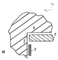
図1の透視図による概略表現によれば、ミラー100が複数のアクセスチャネル110、111、112、...を有し、これらのアクセスチャネルは、ミラーの後面(即ち、ミラー100の光学有効面101とは反対側の面)から「102」で表すミラー基板を通って光学有効面101の付近まで延び、図1によれば、アクセスチャネル110、111、112、...はマトリクス状の配列をなす。図2a〜bでは、1つのアクセスチャネル101のみを断面で示し、ミラー100及び他のアクセスチャネル111、112、...も同様に構成されている。ミラー100またはミラー基板102の光学有効面101上には、反射コーティング(図示せず)が存在する。
According to the schematic representation according to the perspective view of FIG. 1, the
図1、図2、及び他の図面も同様に、それぞれ、定縮尺ではない概略図を表し、ほんの一例として挙げるアクセスチャネル110の寸法は、(本発明をこれらの寸法に限定することなしに)5〜30mmの範囲内の、それぞれの口径を含むことができ、そして、光学有効面101からそれぞれの端面110aまでの距離は、同様に5〜30mmの範囲内である。ミラー100自体の代表的な厚さは、(同様に、ほんの一例であり、本発明を限定することなしに)例えば、約50〜120mmの範囲内である。
1, 2, and other drawings also each represent a schematic diagram that is not to scale, and the dimensions of the
図2aから最も良くわかるように、好適な実施形態では、管状の幾何学的形状の冷却素子120がアクセスチャネル110内に延び、この冷却素子120は、(図示しない制御可能な冷却器への接続によって)その冷却能力を可変に設定することができる。図2a〜bに同様に示すように、この装置は熱放射器130の形態の熱源も有し、好適な実施形態では、この熱源が、アクセスチャネル110の、光学有効面101に面した端部に配置され、同様に可変に設定することができる加熱能力を有する。他の実施形態では、熱放射器130を、アクセスチャネル110の異なる領域内に、特にミラーの後面の領域内にも配置して、この場合、アクセスチャネル110によって、あるいはアクセスチャネル110の側壁上の反射によって、熱放射を、好適には「かすり入射」として知られている十分に浅い反射角で結合させることもできる。さらに、以下でさらに詳細に説明するように、上記熱源は、少なくとも1つの加熱ワイヤの形態に構成することもできる。
As best seen in FIG. 2a, in a preferred embodiment, a tubular
再び図1及び2a、bを参照すれば、熱放射器130によって放射され、ミラー基板材料内に結合される電磁放射が、少なくとも2.5μmの波長を有することができ、少なくとも5μmの波長を有することがより好ましく、この波長は、例えば、400℃までの、特に200℃までの範囲内の温度で、低温放射器として知られているものによって実現することができる。他の好適な実施形態では、例えば螺旋巻きしたフィラメント(一般に、3000℃までの動作温度を有する)のような高温放射器を用いることもできる。
Referring again to FIGS. 1 and 2a, b, the electromagnetic radiation emitted by the
図2a〜bにおいて選定した、一方では冷却素子120の、他方では熱放射器130の構成は、特に、ミラー基板材料から(T=−20℃の温度に設定された)冷却素子120への熱伝達が、アクセスチャネル110のほぼ全面に沿って生じるのに対し、熱放射器130による加熱放射(例えば赤外放射)のミラー基板材料内への結合は、端面110aを含むアクセスチャネル110のほとんど端部のみに生じる、という効果を実現する。一方では冷却素子120と、他方では熱放射器130とを組み合わせた使用は、(例えば、投影露光装置の動作中に入射する電磁(EUV)放射の結果として、光学有効面101の領域内の光学的負荷の増加がある際に、)光学有効面101の領域内のミラー基板材料の温度を、関係するミラー基板材料のゼロ交差温度にほぼ相当する一定値に保つことを可能にする。逆に、光学有効面101の領域内で維持される熱平衡とは独立して、ゼロ交差温度から外れ、熱負荷に対するミラー基板材料の十分な感度を可能にする温度、従って、ミラー100の特定の熱作動または熱変形を、(図2a〜bの「下側」領域内にある)光学有効面101の領域から離れた領域内に設定することができる。
The configuration of the
ほんの一例として(本発明をこれに限定することなしに)、光学有効面101の領域内に設定する温度は30℃にすることができ、光学有効面101から離れた領域内は−15℃にすることができ、この場合、ミラー基板材料に応じた線膨張係数の大幅な変化が既に存在する。
By way of example only (without limiting the present invention), the temperature set in the region of the optical
本発明の概念は、特に、一方では冷却素子の冷却能力の、他方では熱源の加熱能力の、独立して実現可能な調整機能を用いて、光学有効面と、ミラーの光学有効面に相当しない表面(例えば、ミラーの背面)との間に熱流束を生成することを含む。この熱流束は、温度勾配、及びこれに関連するミラー基板の熱膨張係数の値の局所的変化を生じさせ、このことは、温度感度の意味で、あるいは変化する熱膨張係数(CTE)の意味でバイメタルと同等のミラー基板の挙動をもたらす。この概念は、図7にも概略的に例示する(図7では、図1と同様の構成要素または部分は同様の参照番号を有する)。図7に示すように、例えばアクセスチャネル110に沿った熱流束、及び光学有効面101とミラー100の後面との間に生成される温度勾配は、ミラー100の光学有効面101を、光学系の動作中に発生する熱負荷に対してミラー材料がほぼ無感度である温度(即ち、いわゆるゼロ交差温度)に維持することを可能にすると同時に、ミラー基板の光学有効面から離れた領域を、異なるCTE値に起因して、より高感度またはより熱作動可能にして、ミラーの所望の特定変形を生成することを可能にする。
The concept of the present invention does not correspond to the optically effective surface and the optically effective surface of the mirror, in particular by means of an independently realizable adjustment function of the cooling capacity of the cooling element on the one hand and the heating capacity of the heat source on the other hand. Generating heat flux with a surface (eg, the back of the mirror). This heat flux causes a local change in the temperature gradient and the associated value of the coefficient of thermal expansion of the mirror substrate, which means in the sense of temperature sensitivity or the meaning of the changing coefficient of thermal expansion (CTE). This brings about the same mirror substrate behavior as bimetal. This concept is also schematically illustrated in FIG. 7 (in FIG. 7, components or parts similar to FIG. 1 have similar reference numerals). As shown in FIG. 7, for example, the heat flux along the
本発明の1つの態様によれば、ミラー基板の光学有効面とは反対側に面した(例えば、ミラーの背面にある)領域内に温度変化を生成し、これにより、ミラー基板の当該領域内の熱膨張係数の値によって実現される温度感度に起因してミラー基板の変形が生じ、この変形は、(ゼロ交差温度に近いほぼ一定の温度を有する)光学有効面に機械的に伝達される。 In accordance with one aspect of the present invention, a temperature change is generated in a region facing away from the optically effective surface of the mirror substrate (eg, on the back of the mirror), thereby creating a region within the region of the mirror substrate. Due to the temperature sensitivity realized by the value of the coefficient of thermal expansion of the mirror substrate, a deformation of the mirror substrate occurs and this deformation is mechanically transmitted to the optically effective surface (having a substantially constant temperature close to the zero crossing temperature). .
冷却素子120のすべての基本機能を重畳することによって、所望の変形プロファイルを設定することができる。これは、(線膨張係数の「ゼロ交差点」に近いことに起因する)非線形最適化問題であり、その解は、次のステップを反復的に実行することによって数値的に得ることができる:
a)孔のパターンを生成するステップ;
b)温度動作点について、表面温度及び表面変形についての影響行列を計算するステップ;
c)線形計算により、光学有効面全体にわたって温度分布がゼロ交差温度の近くに保たれるという二次的条件下で所望の変形プロファイルが得られるように、個別の加熱能力及び冷却能力を決定するステップ;
d)非線形計算によって、実際の変形プロファイルを決定するステップ;及び、
e)線形計算による変形プロファイルの偏差を修正するように、温度プロファイルを変更するステップ。
By superimposing all the basic functions of the
a) generating a pattern of holes;
b) calculating an influence matrix for the surface temperature and surface deformation for the temperature operating point;
c) Determine the individual heating and cooling capacities so that the desired deformation profile is obtained under linear conditions that the temperature distribution is kept near the zero crossing temperature over the entire optical effective surface by linear calculation. Step;
d) determining the actual deformation profile by non-linear calculation; and
e) changing the temperature profile to correct the deviation of the deformation profile due to linear calculation;
図2c〜fに、影響行列の計算の結果を、ほんの一例として、冷却素子及び関連するアクセスチャネルについて等高線図の形式で示し、図2cはプロファイルdT/dTfを示し、図2dはプロファイルdw/dqfを示し、図2eはプロファイルdT/dTfを示し、図2fはプロファイルdw/dTfを示し、ここにwはz変形(=z方向の変形)を表し、qは熱流を表し、Tは温度を表す。上述したように、対応する影響行列(及び結果的な温度ベースの関数及び変形ベースの関数)どうしを適切に組み合わせて、所望の(できる限り均一な)温度プロファイル、及び所望の変形プロファイルも設定することができる。 FIGS. 2c- f show the results of the influence matrix calculation in contour diagram form for the cooling element and associated access channel, by way of example only, FIG. 2c shows the profile dT / dT f and FIG. 2d shows the profile dw / 2 d shows the profile dT / dT f , FIG. 2 f shows the profile dw / dT f , where w represents the z deformation (= deformation in the z direction), q represents the heat flow, T Represents temperature. As described above, the corresponding influence matrix (and the resulting temperature-based and deformation-based functions) are appropriately combined to set the desired (as uniform as possible) temperature profile and the desired deformation profile. be able to.
ステップd)及びe)を反復的または逐次的に実行することによって、得られる変形の偏差が小さくなっていく。この関係では、例えば、±0.5nmのオーダーの変形が実現可能である。 By performing steps d) and e) repetitively or sequentially, the resulting deformation deviation is reduced. In this relationship, for example, deformation on the order of ± 0.5 nm can be realized.
図3に、異なるミラー基板材料について、温度に応じた線膨張係数をプロットした図を示す。対応する曲線のゼロ交差点のそれぞれが、ゼロ交差温度に相当し、ULE(登録商標)については、およそT=30℃の所にある。熱放射器130によって結合される加熱能力と、冷却素子120によって設定される冷却能力との適切な組合せを適切に選定した結果として、ミラー基板102の光学有効面101付近の領域がこのゼロ交差温度であれば、ミラー基板材料の線膨張係数が0に等しいので、投影露光装置の動作中に光学有効面101上に入射する電磁放射によって生じる光学的負荷が少しも変形を生じさせない。逆に、図3によれば、この温度からの偏差があると、それぞれのミラー基板の温度変化に対する感度の増加があり、このことを、上述したミラー100の熱作動または熱変形に用いることができる。
FIG. 3 shows a plot of linear expansion coefficients according to temperature for different mirror substrate materials. Each of the corresponding curve zero-crossings corresponds to a zero-crossing temperature, and for ULE®, at approximately T = 30 ° C. As a result of proper selection of an appropriate combination of the heating capability coupled by the
以下、本発明の他の実施形態を、図4を参照しながら説明し、図2と同様の、あるいは同じ機能を有する構成要素は、対応する参照番号に「100」を加えて表す。 Hereinafter, another embodiment of the present invention will be described with reference to FIG. 4, and components having the same or the same functions as those in FIG. 2 are represented by adding “100” to the corresponding reference numerals.
図4による実施形態は、図2による実施形態とは、ミラー基板202が2つの異なるミラー基板材料で製造され、従ってミラー200が「複合ミラー」として形成されている点が異なる。実際に、ミラー基板202は第1ミラー基板領域202a及び第2ミラー基板領域202bを有し、第2ミラー基板領域202bは、第1ミラー基板領域202aに対して、ミラー200の光学有効面201からより離れ、ミラー基板領域202a、202bは異なる材料で製造される。実際の好適な実施形態では、第1ミラー基板領域のミラー基板材料がULE(登録商標)であり、第2ミラー基板領域のミラー基板材料が石英ガラス(SiO2)である。しかし、本発明はこれらの材料に限定されず、このため、他の実施形態では、ミラー基板領域202a、202bを異なるミラー基板材料で製造することもでき、いずれの場合にも、第2ミラー基板領域202bのミラー基板材料は、第1ミラー基板領域のミラー基板材料よりも、所定温度における絶対量の意味で大きい線膨張係数を有する。
The embodiment according to FIG. 4 differs from the embodiment according to FIG. 2 in that the mirror substrate 202 is made of two different mirror substrate materials and thus the mirror 200 is formed as a “composite mirror”. Actually, the mirror substrate 202 has a first
図4の好適な実施形態におけるこうした構成の結果として、ミラー基板材料内に形成される温度勾配に起因するだけでなく、異なるミラー基板材料間の遷移にも起因して、上述した、特定変形の目的で望ましい所望のミラー基板材料の感度が、光学有効面201からより離れた領域内に得られ、このため、図4による実施形態は、上記温度勾配だけでは、光学有効面においてゼロ交差温度を維持すると同時に、変形にとって望ましい熱負荷に対する感度を実現するにはまだ十分でない状況に、特に適している。
As a result of such a configuration in the preferred embodiment of FIG. 4, not only due to temperature gradients formed in the mirror substrate material, but also due to the transition between different mirror substrate materials, The desired mirror substrate material sensitivity desired for the purpose is obtained in a region farther from the optically
図5a及び5bは、本発明の実施形態を説明するのに役立つ。図5aによれば、アクセスチャネル110内に結合される熱放射の少なくとも部分的な吸収用の吸収層530が、ミラー基板102と反射コーティング550との間に配置されている。図5bによれば、上述した実施形態に存在する熱放射器130の代わりに、加熱ワイヤの配列540を熱源として設け、これによって、ミラー基板102と反射コーティング550との間の領域を、可変に設定することができる加熱能力で直接加熱することができる。
Figures 5a and 5b serve to illustrate embodiments of the present invention. According to FIG. 5 a, an absorbing
本発明によるミラーの熱作動用の装置は、照明装置内のミラー及びマイクロリソグラフィー投影露光装置の投射レンズ内のミラーに、共に関連して用いることができる。図6に、応用のほんの一例として、米国特許出願公開第2008/0170310号明細書(特許文献7)に開示されている投射レンズ600の光線の経路を示す(図2参照)。投射レンズ600は、EUVにおける動作用に設計され、6つのミラーM1〜M6を有する。この場合、上述した実施形態の1つによれば、例えば、それぞれが瞳孔に近いミラーM2及びM6、さもなければこれらのミラーの他方を、熱作動可能なように構成することができる。
The device for thermal actuation of a mirror according to the invention can be used in conjunction with a mirror in an illumination device and a mirror in a projection lens of a microlithographic projection exposure apparatus. FIG. 6 shows a ray path of the
本発明を特定実施形態に基づいて説明してきたが、例えば、個別の実施形態の特徴を組み合わせること、及び/または交換することによる多数の変形または代案実施形態が、当業者にとって明らかである。従って、こうした変形及び代案実施形態も本発明によってカバーされることは、当業者にとって言うまでもなく、本発明の範囲は、添付する特許請求の範囲またはその等価物のみによって限定される。
Although the present invention has been described with reference to particular embodiments, numerous variations or alternative embodiments will be apparent to those skilled in the art, for example, by combining and / or exchanging features of the individual embodiments. Thus, it should be understood by those skilled in the art that such variations and alternative embodiments are also covered by the present invention, and the scope of the present invention is limited only by the appended claims or their equivalents.
Claims (25)
可変に設定することができる冷却能力を有する冷却素子(120, 220)が、前記少なくとも1つのアクセスチャネル(110, 111, 112, 210)内に突出し、
可変に設定することができる加熱能力を、前記ミラー基板(102, 202)の前記光学有効面に隣接した領域内に結合させるための少なくとも1つの熱源が設けられ、
前記熱源が、加熱放射を前記少なくとも1つのアクセスチャネル(110, 210)内に結合させるための少なくとも1つの熱放射器(130, 230)を有し、
前記少なくとも1つの熱放射器(130, 230)が、前記アクセスチャネル(110, 111, 112,210)の、前記光学有効面に面した端部に配置されており、
前記冷却素子は前記熱源に接触せず、
前記冷却素子(120, 220)の前記冷却能力、及び前記少なくとも1つの熱源の前記加熱能力を設定することによって、前記光学有効面(101, 201)と、前記ミラー(100)の前記光学有効面に相当しない表面との間に熱流束が実現可能になり、この熱流束は、温度勾配、及び当該温度勾配に関連する前記ミラー基板(102, 202)の熱膨張係数の値の局所的変化を生じさせることを特徴とする装置。 An apparatus for thermal operation of a mirror in an optical system in a microlithography projection exposure apparatus, the mirror having a mirror substrate (102, 202) and an optically effective surface (101, 201), the mirror (100 ) At least one access channel (110, 111, 112, 210) extending from the surface not corresponding to the optical effective surface in the direction of the optical effective surface (101, 201),
A cooling element (120, 220) having a cooling capacity that can be variably set protrudes into said at least one access channel (110, 111, 112, 210);
At least one heat source is provided for coupling a heating capacity that can be variably set in a region adjacent to the optically effective surface of the mirror substrate (102, 202);
The heat source comprises at least one heat radiator (130, 230) for coupling heating radiation into the at least one access channel (110, 210);
The at least one heat radiator (130, 230) is disposed at an end of the access channel (110, 111, 112, 210) facing the optically effective surface;
The cooling element does not contact the heat source;
By setting the cooling capacity of the cooling element (120, 220) and the heating capacity of the at least one heat source, the optical effective surface (101, 201) and the optical effective surface of the mirror (100) A heat flux can be realized between the surface and the surface not corresponding to the temperature gradient, and the heat flux is a local change in the temperature gradient and the value of the coefficient of thermal expansion of the mirror substrate (102, 202) related to the temperature gradient. A device characterized by generating.
The device according to claim 6 , characterized in that the heating capacities of the heat radiators (130, 230) can be set independently of each other.
請求項1〜17のいずれかに記載の装置を有する光学系。 An optical system in a microlithographic projection exposure apparatus,
An optical system having a device according to any one of claims 1 to 17.
少なくとも1つの熱源によって、加熱能力を、前記ミラー基板の前記光学有効面に隣接した領域内に結合し、
前記熱源が、加熱放射を前記少なくとも1つのアクセスチャネル(110, 210)内に結合させるための少なくとも1つの熱放射器(130, 230)を有し、
前記少なくとも1つの熱放射器(130, 230)が、前記アクセスチャネル(110, 111, 112,210)の、前記光学有効面に面した端部に配置されており、
前記冷却素子は前記熱源に接触せず、
前記熱源の前記加熱能力及び/または前記冷却素子(102, 202)の前記冷却能力を変化させることによって、前記ミラーの所定の変形プロファイルを生成し、
前記熱源(130, 230, 540)の前記加熱能力及び/または前記冷却素子(120, 220)の前記冷却能力を変化させることは、前記ミラー(100)の前記光学有効面の領域内の温度が、±3K以内で一定値に保たれるように実行することを特徴とする方法。 A method of thermally operating a mirror in an optical system in a microlithography projection exposure apparatus, wherein the mirror (100) includes a mirror substrate (102, 202), an optical effective surface (101, 201), and the mirror (100 ) Having at least one access channel (110, 111, 112, 210) extending from the surface not corresponding to the optical effective surface (101, 201) in the direction of the optical effective surface, and the mirror is variably set In the method also comprising a cooling element (120, 220) having a cooling capacity capable of projecting into the access channel,
Coupling heating capability into a region adjacent to the optically effective surface of the mirror substrate by at least one heat source;
The heat source comprises at least one heat radiator (130, 230) for coupling heating radiation into the at least one access channel (110, 210);
The at least one heat radiator (130, 230) is disposed at an end of the access channel (110, 111, 112, 210) facing the optically effective surface;
The cooling element does not contact the heat source;
Generating a predetermined deformation profile of the mirror by changing the heating capacity of the heat source and / or the cooling capacity of the cooling element (102, 202);
Varying the heating capability of the heat source (130, 230, 540) and / or the cooling capability of the cooling element (120, 220) may cause the temperature in the region of the optically effective surface of the mirror (100) to vary. The method is carried out so as to be kept at a constant value within ± 3K.
What is the optically effective surface (101, 201) of the mirror substrate (102, 202) due to a temperature change in a region opposite to the optically effective surface (101, 201) of the mirror substrate (102, 202)? 25. A method as claimed in any of claims 19 to 24 , characterized in that a deformation occurs in the region on the opposite side and this deformation is mechanically transmitted to the optically effective surface (101, 201).
Applications Claiming Priority (5)
| Application Number | Priority Date | Filing Date | Title |
|---|---|---|---|
| US201361781280P | 2013-03-14 | 2013-03-14 | |
| DE102013204427.5 | 2013-03-14 | ||
| US61/781,280 | 2013-03-14 | ||
| DE102013204427.5A DE102013204427A1 (en) | 2013-03-14 | 2013-03-14 | Arrangement for the thermal actuation of a mirror, in particular in a microlithographic projection exposure apparatus |
| PCT/EP2014/054487 WO2014139896A2 (en) | 2013-03-14 | 2014-03-07 | Arrangement for the thermal actuation of a mirror, in particular in a microlithographic projection exposure apparatus |
Publications (3)
| Publication Number | Publication Date |
|---|---|
| JP2016517028A JP2016517028A (en) | 2016-06-09 |
| JP2016517028A5 JP2016517028A5 (en) | 2017-04-13 |
| JP6483626B2 true JP6483626B2 (en) | 2019-03-13 |
Family
ID=51418762
Family Applications (1)
| Application Number | Title | Priority Date | Filing Date |
|---|---|---|---|
| JP2015562046A Active JP6483626B2 (en) | 2013-03-14 | 2014-03-07 | In particular a device for thermal actuation of mirrors in a microlithographic projection exposure apparatus |
Country Status (6)
| Country | Link |
|---|---|
| US (1) | US9798254B2 (en) |
| JP (1) | JP6483626B2 (en) |
| KR (1) | KR102211633B1 (en) |
| CN (1) | CN105190443B (en) |
| DE (1) | DE102013204427A1 (en) |
| WO (1) | WO2014139896A2 (en) |
Families Citing this family (14)
| Publication number | Priority date | Publication date | Assignee | Title |
|---|---|---|---|---|
| DE102013219808A1 (en) * | 2013-09-30 | 2015-04-02 | Heraeus Quarzglas Gmbh & Co. Kg | Spiegelblank for EUV lithography without extension under EUV irradiation |
| DE102014223750A1 (en) * | 2014-11-20 | 2016-05-25 | Carl Zeiss Smt Gmbh | Projection exposure system with at least one manipulator |
| CN106324792B (en) * | 2015-06-19 | 2020-11-03 | 中国科学院大连化学物理研究所 | Phase change cooling reflector suitable for high-power laser |
| DE102015225509A1 (en) * | 2015-12-16 | 2017-06-22 | Carl Zeiss Smt Gmbh | Reflective optical element |
| CN106125298A (en) * | 2016-08-31 | 2016-11-16 | 中国科学院长春光学精密机械与物理研究所 | Contactless space optical remote sensor reflecting mirror surface shape control system |
| NL2020353A (en) * | 2017-04-11 | 2018-10-17 | Asml Netherlands Bv | Lithographic apparatus |
| CN107390346A (en) * | 2017-09-19 | 2017-11-24 | 北京仿真中心 | A kind of infrared field lens device of Low emissivity |
| DE102019219231A1 (en) | 2019-12-10 | 2020-01-23 | Carl Zeiss Smt Gmbh | Projection exposure system for semiconductor lithography |
| DE102019219289A1 (en) | 2019-12-11 | 2021-06-17 | Carl Zeiss Smt Gmbh | Optical system, as well as heating arrangement and method for heating an optical element in an optical system |
| EP4002009A1 (en) * | 2020-11-11 | 2022-05-25 | ASML Netherlands B.V. | A method and apparatus for thermally deforming an optical surface of an optical element |
| CN116368436A (en) * | 2020-11-11 | 2023-06-30 | Asml荷兰有限公司 | Method and apparatus for thermally deforming optical element |
| DE102021201258A1 (en) | 2021-02-10 | 2022-08-11 | Carl Zeiss Smt Gmbh | Method for heating an optical element in a microlithographic projection exposure system, and optical system |
| DE102021213458A1 (en) | 2021-11-30 | 2022-08-18 | Carl Zeiss Smt Gmbh | Projection exposure system for semiconductor lithography |
| CN114924378B (en) * | 2022-05-30 | 2023-10-27 | 深圳综合粒子设施研究院 | Mirror surface shape control structure and beam line device |
Family Cites Families (22)
| Publication number | Priority date | Publication date | Assignee | Title |
|---|---|---|---|---|
| JPH0868898A (en) * | 1994-08-29 | 1996-03-12 | Nikon Corp | Reflection mirror and its production method |
| JP2004056125A (en) * | 2002-06-20 | 2004-02-19 | Nikon Corp | Reflective projection optical system with discrete actuator |
| US6880942B2 (en) * | 2002-06-20 | 2005-04-19 | Nikon Corporation | Adaptive optic with discrete actuators for continuous deformation of a deformable mirror system |
| EP1376239A3 (en) | 2002-06-25 | 2005-06-29 | Nikon Corporation | Cooling device for an optical element |
| JP2005019628A (en) * | 2003-06-25 | 2005-01-20 | Nikon Corp | Optical apparatus, aligner, manufacturing method of device |
| EP1522892B1 (en) * | 2003-10-09 | 2007-08-29 | ASML Netherlands B.V. | Lithographic apparatus and device manufacturing method |
| JP4537087B2 (en) * | 2004-02-12 | 2010-09-01 | キヤノン株式会社 | Exposure apparatus and device manufacturing method |
| DE102006045075A1 (en) | 2006-09-21 | 2008-04-03 | Carl Zeiss Smt Ag | Controllable optical element |
| EP1950594A1 (en) | 2007-01-17 | 2008-07-30 | Carl Zeiss SMT AG | Imaging optical system, projection illumination unit for microlithography with such an optical system, method for manufacturing a microstructured component with such a projection illumination unit, microstructured component produced by the manufacturing method and use of such an optical system |
| US7894038B2 (en) | 2007-03-14 | 2011-02-22 | Asml Netherlands B.V. | Device manufacturing method, lithographic apparatus, and a computer program |
| EP2181357A1 (en) * | 2007-08-24 | 2010-05-05 | Carl Zeiss SMT AG | Controllable optical element and method for operating an optical element with thermal actuators and projection exposure apparatus for semiconductor lithography |
| KR20170116248A (en) | 2007-10-09 | 2017-10-18 | 칼 짜이스 에스엠테 게엠베하 | Device for controlling temperature of an optical element |
| US7740362B1 (en) * | 2008-02-19 | 2010-06-22 | Jefferson Science Associates | Mirror with thermally controlled radius of curvature |
| WO2009152959A1 (en) | 2008-06-17 | 2009-12-23 | Carl Zeiss Smt Ag | Projection exposure apparatus for semiconductor lithography comprising a device for the thermal manipulation of an optical element |
| US20100033704A1 (en) | 2008-08-11 | 2010-02-11 | Masayuki Shiraishi | Deformable mirror, mirror apparatus, and exposure apparatus |
| DE102009039400A1 (en) | 2009-08-31 | 2011-03-03 | Carl Zeiss Laser Optics Gmbh | Reflective optical element for use in an EUV system |
| JP5732257B2 (en) * | 2010-01-15 | 2015-06-10 | エーエスエムエル ネザーランズ ビー.ブイ. | Lithographic apparatus, device manufacturing method and computer-readable medium |
| JP5785419B2 (en) * | 2010-04-07 | 2015-09-30 | エーエスエムエル ネザーランズ ビー.ブイ. | Method of cooling an optical element, lithographic apparatus, and method of manufacturing a device |
| JP5941463B2 (en) * | 2010-07-30 | 2016-06-29 | カール・ツァイス・エスエムティー・ゲーエムベーハー | EUV exposure equipment |
| DE102011081259A1 (en) | 2010-09-28 | 2012-03-29 | Carl Zeiss Smt Gmbh | Arrangement for mirror temperature measurement and / or for thermal actuation of a mirror in a microlithographic projection exposure apparatus |
| DE102011005778A1 (en) | 2011-03-18 | 2012-09-20 | Carl Zeiss Smt Gmbh | Optical element |
| DE102011005840A1 (en) * | 2011-03-21 | 2012-09-27 | Carl Zeiss Smt Gmbh | A controllable multi-mirror arrangement, optical system with a controllable multi-mirror arrangement and method for operating a controllable multi-mirror arrangement |
-
2013
- 2013-03-14 DE DE102013204427.5A patent/DE102013204427A1/en not_active Withdrawn
-
2014
- 2014-03-07 KR KR1020157026654A patent/KR102211633B1/en active IP Right Grant
- 2014-03-07 JP JP2015562046A patent/JP6483626B2/en active Active
- 2014-03-07 CN CN201480014966.9A patent/CN105190443B/en active Active
- 2014-03-07 WO PCT/EP2014/054487 patent/WO2014139896A2/en active Application Filing
-
2015
- 2015-09-09 US US14/848,593 patent/US9798254B2/en active Active
Also Published As
| Publication number | Publication date |
|---|---|
| JP2016517028A (en) | 2016-06-09 |
| KR20150132203A (en) | 2015-11-25 |
| KR102211633B1 (en) | 2021-02-04 |
| WO2014139896A2 (en) | 2014-09-18 |
| DE102013204427A1 (en) | 2014-09-18 |
| US20160041480A1 (en) | 2016-02-11 |
| US9798254B2 (en) | 2017-10-24 |
| CN105190443A (en) | 2015-12-23 |
| WO2014139896A3 (en) | 2014-11-06 |
| CN105190443B (en) | 2019-04-23 |
Similar Documents
| Publication | Publication Date | Title |
|---|---|---|
| JP6483626B2 (en) | In particular a device for thermal actuation of mirrors in a microlithographic projection exposure apparatus | |
| US10684551B2 (en) | EUV exposure apparatus with reflective elements having reduced influence of temperature variation | |
| JP5902694B2 (en) | Structure for mirror temperature measurement and / or thermal operation of a mirror of a microlithographic projection exposure apparatus | |
| TWI626478B (en) | Mirror arrangement for an euv projection exposure apparatus, method for operating the same, and euv projection exposure apparatus | |
| KR102073038B1 (en) | Optical arrangement for euv lithography | |
| KR20090125042A (en) | Method for improving imaging properties of an optical system, and optical system | |
| TWI564611B (en) | Element arrangement for thermal actuation of a mirror in a microlithographic projection exposure apparatus and actuation method thereof | |
| JP2007524214A (en) | EUV projection lens having a mirror made of a material having a different sign of inclination with respect to a temperature rise in accordance with a thermal expansion coefficient around a zero transition temperature | |
| TW202234139A (en) | A method and apparatus for thermally deforming an optical element | |
| TW202209010A (en) | Optical system and method of operating an optical system | |
| US20160085047A1 (en) | Deformable optical system and method for controlling the same as well as a lithographic system comprising the deformable optical system | |
| EP4002009A1 (en) | A method and apparatus for thermally deforming an optical surface of an optical element | |
| JP2024506046A (en) | Method and optical system for heating optical elements of microlithography projection exposure apparatus | |
| CN116830003A (en) | Optical system and method for operating an optical system |
Legal Events
| Date | Code | Title | Description |
|---|---|---|---|
| A521 | Request for written amendment filed |
Free format text: JAPANESE INTERMEDIATE CODE: A523 Effective date: 20170306 |
|
| A621 | Written request for application examination |
Free format text: JAPANESE INTERMEDIATE CODE: A621 Effective date: 20170306 |
|
| A977 | Report on retrieval |
Free format text: JAPANESE INTERMEDIATE CODE: A971007 Effective date: 20180126 |
|
| A131 | Notification of reasons for refusal |
Free format text: JAPANESE INTERMEDIATE CODE: A131 Effective date: 20180206 |
|
| A521 | Request for written amendment filed |
Free format text: JAPANESE INTERMEDIATE CODE: A523 Effective date: 20180425 |
|
| A02 | Decision of refusal |
Free format text: JAPANESE INTERMEDIATE CODE: A02 Effective date: 20180925 |
|
| A521 | Request for written amendment filed |
Free format text: JAPANESE INTERMEDIATE CODE: A523 Effective date: 20181217 |
|
| A911 | Transfer to examiner for re-examination before appeal (zenchi) |
Free format text: JAPANESE INTERMEDIATE CODE: A911 Effective date: 20181226 |
|
| TRDD | Decision of grant or rejection written | ||
| A01 | Written decision to grant a patent or to grant a registration (utility model) |
Free format text: JAPANESE INTERMEDIATE CODE: A01 Effective date: 20190122 |
|
| A61 | First payment of annual fees (during grant procedure) |
Free format text: JAPANESE INTERMEDIATE CODE: A61 Effective date: 20190214 |
|
| R150 | Certificate of patent or registration of utility model |
Ref document number: 6483626 Country of ref document: JP Free format text: JAPANESE INTERMEDIATE CODE: R150 |
|
| R250 | Receipt of annual fees |
Free format text: JAPANESE INTERMEDIATE CODE: R250 |
|
| R250 | Receipt of annual fees |
Free format text: JAPANESE INTERMEDIATE CODE: R250 |
|
| R250 | Receipt of annual fees |
Free format text: JAPANESE INTERMEDIATE CODE: R250 |