JP6471676B2 - Coated solder wire and manufacturing method thereof - Google Patents
Coated solder wire and manufacturing method thereof Download PDFInfo
- Publication number
- JP6471676B2 JP6471676B2 JP2015212063A JP2015212063A JP6471676B2 JP 6471676 B2 JP6471676 B2 JP 6471676B2 JP 2015212063 A JP2015212063 A JP 2015212063A JP 2015212063 A JP2015212063 A JP 2015212063A JP 6471676 B2 JP6471676 B2 JP 6471676B2
- Authority
- JP
- Japan
- Prior art keywords
- solder wire
- coated
- solder
- mass
- radicalized
- Prior art date
- Legal status (The legal status is an assumption and is not a legal conclusion. Google has not performed a legal analysis and makes no representation as to the accuracy of the status listed.)
- Expired - Fee Related
Links
Images

Classifications
-
- C—CHEMISTRY; METALLURGY
- C22—METALLURGY; FERROUS OR NON-FERROUS ALLOYS; TREATMENT OF ALLOYS OR NON-FERROUS METALS
- C22C—ALLOYS
- C22C18/00—Alloys based on zinc
- C22C18/04—Alloys based on zinc with aluminium as the next major constituent
-
- B—PERFORMING OPERATIONS; TRANSPORTING
- B05—SPRAYING OR ATOMISING IN GENERAL; APPLYING FLUENT MATERIALS TO SURFACES, IN GENERAL
- B05D—PROCESSES FOR APPLYING FLUENT MATERIALS TO SURFACES, IN GENERAL
- B05D1/00—Processes for applying liquids or other fluent materials
- B05D1/62—Plasma-deposition of organic layers
-
- B—PERFORMING OPERATIONS; TRANSPORTING
- B23—MACHINE TOOLS; METAL-WORKING NOT OTHERWISE PROVIDED FOR
- B23K—SOLDERING OR UNSOLDERING; WELDING; CLADDING OR PLATING BY SOLDERING OR WELDING; CUTTING BY APPLYING HEAT LOCALLY, e.g. FLAME CUTTING; WORKING BY LASER BEAM
- B23K35/00—Rods, electrodes, materials, or media, for use in soldering, welding, or cutting
- B23K35/02—Rods, electrodes, materials, or media, for use in soldering, welding, or cutting characterised by mechanical features, e.g. shape
- B23K35/0222—Rods, electrodes, materials, or media, for use in soldering, welding, or cutting characterised by mechanical features, e.g. shape for use in soldering, brazing
- B23K35/0227—Rods, wires
-
- B—PERFORMING OPERATIONS; TRANSPORTING
- B23—MACHINE TOOLS; METAL-WORKING NOT OTHERWISE PROVIDED FOR
- B23K—SOLDERING OR UNSOLDERING; WELDING; CLADDING OR PLATING BY SOLDERING OR WELDING; CUTTING BY APPLYING HEAT LOCALLY, e.g. FLAME CUTTING; WORKING BY LASER BEAM
- B23K35/00—Rods, electrodes, materials, or media, for use in soldering, welding, or cutting
- B23K35/22—Rods, electrodes, materials, or media, for use in soldering, welding, or cutting characterised by the composition or nature of the material
- B23K35/24—Selection of soldering or welding materials proper
- B23K35/26—Selection of soldering or welding materials proper with the principal constituent melting at less than 400 degrees C
- B23K35/262—Sn as the principal constituent
-
- B—PERFORMING OPERATIONS; TRANSPORTING
- B23—MACHINE TOOLS; METAL-WORKING NOT OTHERWISE PROVIDED FOR
- B23K—SOLDERING OR UNSOLDERING; WELDING; CLADDING OR PLATING BY SOLDERING OR WELDING; CUTTING BY APPLYING HEAT LOCALLY, e.g. FLAME CUTTING; WORKING BY LASER BEAM
- B23K35/00—Rods, electrodes, materials, or media, for use in soldering, welding, or cutting
- B23K35/22—Rods, electrodes, materials, or media, for use in soldering, welding, or cutting characterised by the composition or nature of the material
- B23K35/24—Selection of soldering or welding materials proper
- B23K35/26—Selection of soldering or welding materials proper with the principal constituent melting at less than 400 degrees C
- B23K35/268—Pb as the principal constituent
-
- B—PERFORMING OPERATIONS; TRANSPORTING
- B23—MACHINE TOOLS; METAL-WORKING NOT OTHERWISE PROVIDED FOR
- B23K—SOLDERING OR UNSOLDERING; WELDING; CLADDING OR PLATING BY SOLDERING OR WELDING; CUTTING BY APPLYING HEAT LOCALLY, e.g. FLAME CUTTING; WORKING BY LASER BEAM
- B23K35/00—Rods, electrodes, materials, or media, for use in soldering, welding, or cutting
- B23K35/22—Rods, electrodes, materials, or media, for use in soldering, welding, or cutting characterised by the composition or nature of the material
- B23K35/24—Selection of soldering or welding materials proper
- B23K35/28—Selection of soldering or welding materials proper with the principal constituent melting at less than 950 degrees C
- B23K35/282—Zn as the principal constituent
-
- B—PERFORMING OPERATIONS; TRANSPORTING
- B23—MACHINE TOOLS; METAL-WORKING NOT OTHERWISE PROVIDED FOR
- B23K—SOLDERING OR UNSOLDERING; WELDING; CLADDING OR PLATING BY SOLDERING OR WELDING; CUTTING BY APPLYING HEAT LOCALLY, e.g. FLAME CUTTING; WORKING BY LASER BEAM
- B23K35/00—Rods, electrodes, materials, or media, for use in soldering, welding, or cutting
- B23K35/22—Rods, electrodes, materials, or media, for use in soldering, welding, or cutting characterised by the composition or nature of the material
- B23K35/36—Selection of non-metallic compositions, e.g. coatings, fluxes; Selection of soldering or welding materials, conjoint with selection of non-metallic compositions, both selections being of interest
- B23K35/3601—Selection of non-metallic compositions, e.g. coatings, fluxes; Selection of soldering or welding materials, conjoint with selection of non-metallic compositions, both selections being of interest with inorganic compounds as principal constituents
- B23K35/3611—Phosphates
-
- B—PERFORMING OPERATIONS; TRANSPORTING
- B23—MACHINE TOOLS; METAL-WORKING NOT OTHERWISE PROVIDED FOR
- B23K—SOLDERING OR UNSOLDERING; WELDING; CLADDING OR PLATING BY SOLDERING OR WELDING; CUTTING BY APPLYING HEAT LOCALLY, e.g. FLAME CUTTING; WORKING BY LASER BEAM
- B23K35/00—Rods, electrodes, materials, or media, for use in soldering, welding, or cutting
- B23K35/22—Rods, electrodes, materials, or media, for use in soldering, welding, or cutting characterised by the composition or nature of the material
- B23K35/36—Selection of non-metallic compositions, e.g. coatings, fluxes; Selection of soldering or welding materials, conjoint with selection of non-metallic compositions, both selections being of interest
- B23K35/365—Selection of non-metallic compositions of coating materials either alone or conjoint with selection of soldering or welding materials
-
- B—PERFORMING OPERATIONS; TRANSPORTING
- B23—MACHINE TOOLS; METAL-WORKING NOT OTHERWISE PROVIDED FOR
- B23K—SOLDERING OR UNSOLDERING; WELDING; CLADDING OR PLATING BY SOLDERING OR WELDING; CUTTING BY APPLYING HEAT LOCALLY, e.g. FLAME CUTTING; WORKING BY LASER BEAM
- B23K35/00—Rods, electrodes, materials, or media, for use in soldering, welding, or cutting
- B23K35/40—Making wire or rods for soldering or welding
-
- C—CHEMISTRY; METALLURGY
- C22—METALLURGY; FERROUS OR NON-FERROUS ALLOYS; TREATMENT OF ALLOYS OR NON-FERROUS METALS
- C22C—ALLOYS
- C22C11/00—Alloys based on lead
-
- C—CHEMISTRY; METALLURGY
- C22—METALLURGY; FERROUS OR NON-FERROUS ALLOYS; TREATMENT OF ALLOYS OR NON-FERROUS METALS
- C22C—ALLOYS
- C22C13/00—Alloys based on tin
-
- C—CHEMISTRY; METALLURGY
- C23—COATING METALLIC MATERIAL; COATING MATERIAL WITH METALLIC MATERIAL; CHEMICAL SURFACE TREATMENT; DIFFUSION TREATMENT OF METALLIC MATERIAL; COATING BY VACUUM EVAPORATION, BY SPUTTERING, BY ION IMPLANTATION OR BY CHEMICAL VAPOUR DEPOSITION, IN GENERAL; INHIBITING CORROSION OF METALLIC MATERIAL OR INCRUSTATION IN GENERAL
- C23C—COATING METALLIC MATERIAL; COATING MATERIAL WITH METALLIC MATERIAL; SURFACE TREATMENT OF METALLIC MATERIAL BY DIFFUSION INTO THE SURFACE, BY CHEMICAL CONVERSION OR SUBSTITUTION; COATING BY VACUUM EVAPORATION, BY SPUTTERING, BY ION IMPLANTATION OR BY CHEMICAL VAPOUR DEPOSITION, IN GENERAL
- C23C4/00—Coating by spraying the coating material in the molten state, e.g. by flame, plasma or electric discharge
- C23C4/04—Coating by spraying the coating material in the molten state, e.g. by flame, plasma or electric discharge characterised by the coating material
-
- C—CHEMISTRY; METALLURGY
- C23—COATING METALLIC MATERIAL; COATING MATERIAL WITH METALLIC MATERIAL; CHEMICAL SURFACE TREATMENT; DIFFUSION TREATMENT OF METALLIC MATERIAL; COATING BY VACUUM EVAPORATION, BY SPUTTERING, BY ION IMPLANTATION OR BY CHEMICAL VAPOUR DEPOSITION, IN GENERAL; INHIBITING CORROSION OF METALLIC MATERIAL OR INCRUSTATION IN GENERAL
- C23C—COATING METALLIC MATERIAL; COATING MATERIAL WITH METALLIC MATERIAL; SURFACE TREATMENT OF METALLIC MATERIAL BY DIFFUSION INTO THE SURFACE, BY CHEMICAL CONVERSION OR SUBSTITUTION; COATING BY VACUUM EVAPORATION, BY SPUTTERING, BY ION IMPLANTATION OR BY CHEMICAL VAPOUR DEPOSITION, IN GENERAL
- C23C4/00—Coating by spraying the coating material in the molten state, e.g. by flame, plasma or electric discharge
- C23C4/12—Coating by spraying the coating material in the molten state, e.g. by flame, plasma or electric discharge characterised by the method of spraying
- C23C4/134—Plasma spraying
-
- C—CHEMISTRY; METALLURGY
- C23—COATING METALLIC MATERIAL; COATING MATERIAL WITH METALLIC MATERIAL; CHEMICAL SURFACE TREATMENT; DIFFUSION TREATMENT OF METALLIC MATERIAL; COATING BY VACUUM EVAPORATION, BY SPUTTERING, BY ION IMPLANTATION OR BY CHEMICAL VAPOUR DEPOSITION, IN GENERAL; INHIBITING CORROSION OF METALLIC MATERIAL OR INCRUSTATION IN GENERAL
- C23C—COATING METALLIC MATERIAL; COATING MATERIAL WITH METALLIC MATERIAL; SURFACE TREATMENT OF METALLIC MATERIAL BY DIFFUSION INTO THE SURFACE, BY CHEMICAL CONVERSION OR SUBSTITUTION; COATING BY VACUUM EVAPORATION, BY SPUTTERING, BY ION IMPLANTATION OR BY CHEMICAL VAPOUR DEPOSITION, IN GENERAL
- C23C4/00—Coating by spraying the coating material in the molten state, e.g. by flame, plasma or electric discharge
- C23C4/18—After-treatment
-
- B—PERFORMING OPERATIONS; TRANSPORTING
- B05—SPRAYING OR ATOMISING IN GENERAL; APPLYING FLUENT MATERIALS TO SURFACES, IN GENERAL
- B05D—PROCESSES FOR APPLYING FLUENT MATERIALS TO SURFACES, IN GENERAL
- B05D2202/00—Metallic substrate
-
- B—PERFORMING OPERATIONS; TRANSPORTING
- B05—SPRAYING OR ATOMISING IN GENERAL; APPLYING FLUENT MATERIALS TO SURFACES, IN GENERAL
- B05D—PROCESSES FOR APPLYING FLUENT MATERIALS TO SURFACES, IN GENERAL
- B05D2518/00—Other type of polymers
-
- B—PERFORMING OPERATIONS; TRANSPORTING
- B05—SPRAYING OR ATOMISING IN GENERAL; APPLYING FLUENT MATERIALS TO SURFACES, IN GENERAL
- B05D—PROCESSES FOR APPLYING FLUENT MATERIALS TO SURFACES, IN GENERAL
- B05D7/00—Processes, other than flocking, specially adapted for applying liquids or other fluent materials to particular surfaces or for applying particular liquids or other fluent materials
- B05D7/20—Processes, other than flocking, specially adapted for applying liquids or other fluent materials to particular surfaces or for applying particular liquids or other fluent materials to wires
Description
本発明は、半導体装置を製造する際に用いるはんだワイヤおよびその製造方法に関する。 The present invention relates to a solder wire used when manufacturing a semiconductor device and a method for manufacturing the solder wire.
半導体素子接合基板や半導体装置などの製造において、金属材料同士を接合する場合に、あるいは、半導体素子などの電子部品をプリント基板に接合する場合に、はんだ付けが一般的に採用される。はんだ付けに使用されるはんだ材料は、ワイヤ、リボン、シート、プリフォーム材(打抜き材)、ボール、微粉末などの種々の形状に成形される。 In manufacturing a semiconductor element bonding substrate, a semiconductor device, or the like, soldering is generally employed when metal materials are bonded to each other or when an electronic component such as a semiconductor element is bonded to a printed circuit board. Solder materials used for soldering are formed into various shapes such as wires, ribbons, sheets, preform materials (punching materials), balls, and fine powders.
はんだ材料は、酸素の存在下で酸化しやすく、保管中に、その表面に酸化膜が形成される。特に、はんだ材料を製造してから長期間経過後に使用する場合には、酸化が進行し、この酸化膜が厚いものとなるため、はんだ材料の濡れ広がり性や接合性の低下、あるいは、空隙(ボイド)の発生などの接合欠陥を招く。加えて、はんだ材料は、使用時に高温で溶融されるため、酸化膜はさらに厚いものとなる。このような分厚い酸化膜が、接合界面に存在すると、接合部に導通不良や接合性の低下といった問題が生ずる。 The solder material is easily oxidized in the presence of oxygen, and an oxide film is formed on the surface during storage. In particular, when the solder material is used after a long period of time since it is manufactured, the oxidation proceeds and the oxide film becomes thick. This causes joint defects such as voids. In addition, since the solder material is melted at a high temperature during use, the oxide film becomes thicker. If such a thick oxide film is present at the bonding interface, problems such as poor conduction and poor bonding occur at the bonded portion.
金属材料や合金材料の酸化を防止する技術として、表面処理により被覆膜を形成する方法が知られている。特に、大気圧プラズマCVD法を用いた表面処理は、比較的低コストで、緻密な被覆膜を形成することができるため、酸化防止効果が高いばかりでなく、成膜材料が室内に拡散することがないため、安全性にも優れることから注目を集めている。 As a technique for preventing oxidation of a metal material or an alloy material, a method of forming a coating film by surface treatment is known. In particular, the surface treatment using the atmospheric pressure plasma CVD method can form a dense coating film at a relatively low cost, so that not only the antioxidant effect is high but also the film forming material diffuses into the room. It has attracted attention because of its superior safety.
たとえば、特表2004−510571号公報には、有機ケイ素化合物からなる噴霧液体コーティング形成材料を大気圧プラズマ放電中に導入し、金属などの基板をこの噴霧コーティング形成材料に晒すことにより、基板の表面に、ポリジメチルシロキサンなどからなるコーティング(被覆膜)を形成する方法が開示されている。 For example, Japanese Patent Publication No. 2004-510571 discloses a substrate surface by introducing a spray liquid coating forming material made of an organosilicon compound into an atmospheric pressure plasma discharge and exposing a substrate such as a metal to the spray coating forming material. Discloses a method of forming a coating (coating film) made of polydimethylsiloxane or the like.
しかしながら、この方法では、反応ガスのプラズマ化と微粒化される噴霧コーティング形成材料の活性化が同時に行われるため、噴霧コーティング形成材料の活性化が不均一なものとなり、基板の表面全面にわたって、緻密な被覆膜を均一に形成することは困難である。また、この方法では、はんだ材料表面の酸化を防止することは意図されておらず、よって、はんだ材料の溶融時における被覆膜の挙動や、被覆膜の存在による濡れ広がり性および接合性への影響について何ら考慮されていない。 However, in this method, the plasma of the reactive gas and the activation of the spray coating forming material that is atomized are performed at the same time, so the activation of the spray coating forming material becomes non-uniform and the entire surface of the substrate is dense. It is difficult to form a uniform coating film uniformly. Further, this method is not intended to prevent the oxidation of the surface of the solder material. Therefore, the behavior of the coating film at the time of melting of the solder material, and the wettability and joining property due to the presence of the coating film are considered. No consideration is given to the effects of.
これに対して、特開2014−195831号公報には、大気圧下でプラズマガス中に、有機ケイ素化合物を、キャリアガスとともに混合噴霧することで、有機ケイ素化合物をラジカル化し、ラジカル化した有機ケイ素化合物を重合させながら、はんだ材料の表面に存在する金属と反応させることで、厚さが4nm〜200nmのポリシロキサンからなる被覆膜を形成する、被覆はんだ材料の製造方法が開示されている。この方法によれば、有機ケイ素化合物を瞬時にラジカル化させることができるため、有機ケイ素化合物の基本骨格を維持したまま、緻密な被覆膜をはんだ材料の表面全体にわたって、均一に形成することができる。このため、この方法では、はんだ材料の濡れ広がり性や接合性を損ねることなく、長期保管時および溶融時における酸化の進行を防止することが可能となる。 On the other hand, Japanese Patent Application Laid-Open No. 2014-195831 discloses radicalizing organosilicon compounds by mixing and spraying an organosilicon compound together with a carrier gas in a plasma gas at atmospheric pressure. A method for producing a coated solder material is disclosed in which a coating film made of polysiloxane having a thickness of 4 nm to 200 nm is formed by reacting with a metal present on the surface of the solder material while polymerizing the compound. According to this method, since the organosilicon compound can be radicalized instantly, a dense coating film can be uniformly formed over the entire surface of the solder material while maintaining the basic skeleton of the organosilicon compound. it can. For this reason, in this method, it is possible to prevent the progress of oxidation during long-term storage and melting without impairing the wetting and joining properties of the solder material.
しかしながら、特開2014−195831号公報に記載の方法を、工業規模の製造にそのまま適用すると、被覆膜全体としての厚さの均一性に改善の余地がある。また、被覆はんだワイヤに対しては、その濡れ広がり性や接合性についてのさらなる改善の要求もある。 However, when the method described in Japanese Patent Application Laid-Open No. 2014-195831 is applied as it is to manufacturing on an industrial scale, there is room for improvement in the uniformity of the thickness of the entire coating film. In addition, there is a demand for further improvement in the wet solderability and bondability of the coated solder wire.
そこで、本発明は、1回の処理によって、緻密な被覆膜をはんだワイヤの表面全体にわたって均一に形成することにより、長期保管時および溶融時に、表面の酸化を防止することができ、かつ、濡れ広がり性や接合性について従来よりもさらに優れた被覆はんだワイヤを、工業規模の製造により効率よく提供することを目的とする。 Therefore, the present invention can prevent oxidation of the surface during long-term storage and melting by forming a dense coating film uniformly over the entire surface of the solder wire by a single treatment, and It is an object to efficiently provide a coated solder wire that is further superior to the conventional one in terms of wetting spreadability and bondability by manufacturing on an industrial scale.
本発明の被覆はんだワイヤは、はんだワイヤと、該はんだワイヤの表面に形成された含リン化合物を主成分として含み、1nm〜100nmの範囲の厚さを有する被覆膜とを備えることを特徴とする。 The coated solder wire of the present invention comprises a solder wire and a coated film containing a phosphorus-containing compound formed on the surface of the solder wire as a main component and having a thickness in the range of 1 nm to 100 nm. To do.
前記被覆膜の厚さは、3nm〜80nmの範囲にあることが好ましく、5nm〜50nmの範囲にあることがより好ましい。 The thickness of the coating film is preferably in the range of 3 nm to 80 nm, and more preferably in the range of 5 nm to 50 nm.
前記被覆膜の厚さの最大値と最小値との差は、2.5nm以下であることが好ましく、2.0nm以下であることがより好ましく、1.5nm以下であることがさらに好ましい。 The difference between the maximum value and the minimum value of the thickness of the coating film is preferably 2.5 nm or less, more preferably 2.0 nm or less, and further preferably 1.5 nm or less.
本発明の被覆はんだワイヤの特性を示す指標として、前記被覆はんだワイヤを用いて、接合温度340℃〜350℃で接合することにより得られた接合はんだにおいて、該接合はんだの平面視における最大径をXとし、該最大径Xの伸長する方向に直交する方向の径をYとし、該接合はんだの高さをZとした場合に、式((X+Y)/2)/Zで求められるアスペクト比をACとし、前記はんだワイヤと同一の組成を有し、かつ未被覆のはんだワイヤについて、前記被覆はんだワイヤと同様に求めたアスペクト比をAnとした場合に、該未被覆はんだワイヤのアスペクト比Anに対する前記被覆はんだワイヤのアスペクト比ACの比(AC/An)を用いることができる。そして、本発明の被覆はんだワイヤの特徴としては、該比(AC/An)が1.6〜3.0の範囲であり、前記未被覆はんだワイヤに対してきわめて高い濡れ広がり性を示すことが挙げられる。 As an index indicating the characteristics of the coated solder wire of the present invention, the maximum diameter in a plan view of the bonding solder obtained by bonding at a bonding temperature of 340 ° C. to 350 ° C. using the coated solder wire. When X is X, Y is the diameter perpendicular to the extending direction of the maximum diameter X, and Z is the height of the solder joint, the aspect ratio calculated by the formula ((X + Y) / 2) / Z is and a C, has the solder wire the same composition as, and the solder wire uncoated, the aspect ratio obtained in the same manner as in the coating solder wire when the a n, the aspect ratio of the yet-coated solder wire it can be used the ratio of the aspect ratio a C of the coating solder wire for a n (a C / a n ). As a feature of the coated solder wire of the present invention, the ratio (A C / A n ) is in the range of 1.6 to 3.0, and exhibits extremely high wet spreadability with respect to the uncoated solder wire. Can be mentioned.
該比(AC/An)は、1.7〜2.8の範囲にあることがより好ましく、1.8〜2.5の範囲にあることがさらに好ましい。 The ratio (A C / A n ) is more preferably in the range of 1.7 to 2.8, and still more preferably in the range of 1.8 to 2.5.
本発明は、さまざまな組成のはんだワイヤに任意に適用可能であるが、特に、本発明は、80質量%以上のPbと、Sn、Ag、Cu、In、Te、およびPからなる群から選択される1種以上の第2元素とを含有し、かつ、Pbと第2元素との含有量が、合計で95質量%以上のはんだ合金からなる、はんだワイヤに好適に適用される。または、本発明は、80質量%以上のSnと、Ag、Sb、Cu、Ni、Ge、およびPからなる群から選択される1種以上の第2元素とを含有し、かつ、Snと第2元素との含有量が、合計で95質量%以上のはんだ合金からなる、はんだワイヤに好適に適用される。 The present invention can be arbitrarily applied to solder wires having various compositions. In particular, the present invention is selected from the group consisting of 80% by mass or more of Pb and Sn, Ag, Cu, In, Te, and P. The present invention is suitably applied to a solder wire that contains one or more second elements and contains a solder alloy having a total content of Pb and the second element of 95% by mass or more. Alternatively, the present invention contains 80% by mass or more of Sn and one or more second elements selected from the group consisting of Ag, Sb, Cu, Ni, Ge, and P, and Sn and It is suitably applied to a solder wire made of a solder alloy having a total content of two elements of 95% by mass or more.
あるいは、本発明は、90質量%以上のZnと、2.0質量%以上9.0質量%以下のAlと、さらにAg、GeおよびPからなる群から選択される1種以上の第3元素とを含有し、Agを含有する場合にはAgの含有量が0.1質量%以上4.0質量%以下、Geを含有する場合にはGeの含有量が0.01質量%以上2.00質量%以下、Pを含有する場合にはPの含有量が0.5000質量%以下であるはんだ合金からなる、はんだワイヤに好適に適用される。 Alternatively, the present invention provides one or more third elements selected from the group consisting of 90% by mass or more of Zn, 2.0% by mass or more and 9.0% by mass or less of Al, and Ag, Ge, and P. When Ag is contained, the Ag content is 0.1% by mass or more and 4.0% by mass or less, and when Ge is contained, the Ge content is 0.01% by mass or more and 2.% by mass. When it contains 00 mass% or less and P, it applies suitably to the solder wire which consists of a solder alloy whose P content is 0.5000 mass% or less.
本発明の被覆はんだワイヤの製造方法は、
大気圧下でプラズマ化された反応ガスと、キャリアガスを介して導入された有機リン化合物とを混合し、該有機リン化合物をラジカル化させて、ラジカル化有機リン化合物を形成する、ラジカル化工程と、
螺旋状のガス流によって画定され、前記ラジカル化有機リン化合物が均一に分散した反応領域を形成する、反応領域形成工程と、
前記反応領域内で、はんだワイヤを搬送し、前記ラジカル化有機リン化合物を該はんだワイヤ表面の金属と反応させることにより、該はんだワイヤ表面に厚さが1nm〜100nmの、含リン化合物を主成分として含む被覆膜を形成する、被覆工程と、
を備えることを特徴とする。
The method for producing the coated solder wire of the present invention is as follows.
A radicalization step in which a reaction gas plasmified under atmospheric pressure and an organophosphorus compound introduced via a carrier gas are mixed and radicalized to form a radicalized organophosphorus compound. When,
A reaction region forming step defined by a spiral gas flow to form a reaction region in which the radicalized organophosphorus compound is uniformly dispersed;
In the reaction region, a solder wire is conveyed, and the radicalized organophosphorus compound is reacted with a metal on the surface of the solder wire to thereby mainly contain a phosphorus-containing compound having a thickness of 1 nm to 100 nm on the surface of the solder wire. Forming a coating film containing as a coating process;
It is characterized by providing.
前記反応領域形成工程において、予め導入した螺旋状のガス流に、前記ラジカル化有機リン化合物を混合することにより、前記反応領域を形成することが好ましい。この場合、前記螺旋状のガス流を、アルゴン、ヘリウム、窒素、酸素、および空気の群から選択される少なくとも1種によって形成することができる。 In the reaction region forming step, the reaction region is preferably formed by mixing the radicalized organophosphorus compound in a spiral gas flow introduced in advance. In this case, the spiral gas flow can be formed by at least one selected from the group consisting of argon, helium, nitrogen, oxygen, and air.
前記有機リン化合物として、リン酸トリメチル、リン酸トリエチル、リン酸トリブチル、リン酸トリペンチル、リン酸水素ビス(2−エチルヘキシル)、リン酸トリフェニル、亜リン酸トリメチル、亜リン酸トリエチル、亜リン酸トリブチル、亜リン酸トリペンチル、亜リン酸水素ビス(2−ノニルフェニル)、亜リン酸トリフェニルから選択される少なくとも1種を用いることができる。 Examples of the organic phosphorus compound include trimethyl phosphate, triethyl phosphate, tributyl phosphate, tripentyl phosphate, bis (2-ethylhexyl) hydrogen phosphate, triphenyl phosphate, trimethyl phosphite, triethyl phosphite, phosphorous acid At least one selected from tributyl, tripentyl phosphite, bis (2-nonylphenyl) hydrogen phosphite, and triphenyl phosphite can be used.
前記反応ガスとしては、アルゴン、ヘリウム、窒素、酸素、および空気の群から選択される少なくとも1種を用いることができる。また、前記キャリアガスとしては、アルゴン、ヘリウム、および窒素から選択される少なくとも1種を用いることができる。 As the reactive gas, at least one selected from the group consisting of argon, helium, nitrogen, oxygen, and air can be used. Further, as the carrier gas, at least one selected from argon, helium, and nitrogen can be used.
前記ラジカル化工程において、大気圧プラズマ重合処理装置により、前記有機リン化合物をラジカル化することが好ましい。 In the radicalization step, the organophosphorus compound is preferably radicalized by an atmospheric pressure plasma polymerization treatment apparatus.
前記ラジカル化工程において、前記はんだワイヤ1mに対する前記有機リン化合物の導入量を0.005g〜0.560gの範囲とすることが好ましい。なお、該有機リン化合物の導入量を0.016g〜0.450gの範囲とすることがより好ましく、0.028g〜0.280gの範囲とすることがさらに好ましい。 In the radicalization step, the amount of the organophosphorus compound introduced into 1 m of the solder wire is preferably in the range of 0.005 g to 0.560 g. The amount of the organophosphorus compound introduced is more preferably in the range of 0.016 g to 0.450 g, and still more preferably in the range of 0.028 g to 0.280 g.
また、前記被覆工程における該はんだワイヤの搬送速度を1m/分〜100m/分とすることが好ましく、5m/分〜80m/分とすることがより好ましく、10m/分〜50m/分とすることがさらに好ましい。 Moreover, it is preferable to set the conveyance speed of the solder wire in the coating step to 1 m / min to 100 m / min, more preferably 5 m / min to 80 m / min, and 10 m / min to 50 m / min. Is more preferable.
本発明によれば、含リン化合物を主成分として含む緻密な被覆膜が、はんだワイヤの表面全体にわたって均一に形成された被覆はんだワイヤが提供される。この被覆はんだワイヤを用いることにより、長期保管時および溶融時に、はんだワイヤ表面の酸化および接合はんだの表面の酸化の両方を効果的に防止することができる。さらに、本発明の被覆はんだワイヤは、被覆膜の主成分として、含リン化合物を採用することにより、従来の未被覆のはんだワイヤあるいはポリシロキサンからなる被覆膜を備えるはんだワイヤと比較して、より優れた濡れ広がり性や接合性を示す。さらに、本発明の被覆はんだワイヤの製造方法によれば、このような被覆はんだワイヤを1回の処理で効率よく得ることができる。したがって、本発明の工業的意義はきわめて大きい。 According to the present invention, there is provided a coated solder wire in which a dense coating film containing a phosphorus-containing compound as a main component is uniformly formed over the entire surface of the solder wire. By using this coated solder wire, both the oxidation of the surface of the solder wire and the oxidation of the surface of the bonding solder can be effectively prevented during long-term storage and melting. Furthermore, the coated solder wire of the present invention employs a phosphorus-containing compound as a main component of the coating film, thereby comparing with a conventional uncoated solder wire or a solder wire having a coating film made of polysiloxane. , Better wet spreadability and bondability. Furthermore, according to the method for producing a coated solder wire of the present invention, such a coated solder wire can be obtained efficiently by a single treatment. Therefore, the industrial significance of the present invention is very great.
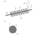
特開2014−195831号公報に開示された方法を工業規模の製造に適用して、長尺のはんだワイヤの表面全体を被覆する場合、図2に示すように、基材となるはんだワイヤ2に対して複数回(図示の例では3回)の被覆処理をすることが必要となる。すなわち、
(a)搬送中におけるはんだワイヤ2の捻れを防止可能な搬送治具7を、面7aが底面側となるよう固定した状態で、はんだワイヤ2を矢印Aの方向に搬送しつつ、ノズル8からラジカル化した有機ケイ素化合物5を噴霧し、被覆膜3aを形成し(図2(a―1)参照)、
(b)次いで、搬送治具7を、面7bが底面側となるように120°回転させた後、(a)と同様にして、被覆膜3bを形成し(図2(b−1)参照)、
(c)最後に、搬送治具7を、面7cが底面側となるようにさらに120°回転させた後、(a)および(b)と同様にして、被覆膜3c形成する(図2(c−1)参照)、
ことが必要となる。
When the method disclosed in Japanese Patent Application Laid-Open No. 2014-195831 is applied to manufacturing on an industrial scale to cover the entire surface of a long solder wire, as shown in FIG. On the other hand, it is necessary to perform a coating process a plurality of times (three times in the illustrated example). That is,
(A) From the
(B) Next, after the conveying
(C) Finally, the conveying
It will be necessary.
このように、特開2014−195831号公報に開示された技術を工業規模の製造に適用した場合、被覆はんだワイヤの生産性が十分でなく、また、図2(a―2)、(b−2)、および(c−2)に示されるように、被覆膜5a〜5cの境界に被覆が薄い部分が生じるため、被覆膜全体としての厚さの均一性についても不十分であるといった問題がある。 As described above, when the technique disclosed in Japanese Patent Application Laid-Open No. 2014-195831 is applied to industrial scale manufacturing, the productivity of the coated solder wire is not sufficient, and FIGS. 2 (a-2) and 2 (b- As shown in 2) and (c-2), a thin portion of the coating occurs at the boundary between the coating films 5a to 5c, and thus the thickness uniformity of the entire coating film is insufficient. There's a problem.
また、特開2014−195831号公報に開示された技術では、被覆膜の材料として、ポリシロキサンを用いている。ポリシロキサンを用いた被覆膜は、従来の未被覆のはんだワイヤと比較すると、長期保管時および溶融時におけるはんだワイヤの酸化の進行を防止する機能のみならず、はんだワイヤに従来と同様の濡れ広がり性および接合性を付与している。しかしながら、はんだワイヤに対しては、濡れ広がり性および接合性のさらなる改善が要求されている。 In the technique disclosed in Japanese Patent Application Laid-Open No. 2014-195831, polysiloxane is used as a material for the coating film. Compared to conventional uncoated solder wires, the coating film using polysiloxane not only has the function of preventing the progress of oxidation of the solder wire during long-term storage and melting, but also has the same wettability as before. Adds spreadability and bondability. However, the solder wire is required to be further improved in wet spreadability and bondability.
本発明者らは、上述した課題について検討を重ねた結果、被覆膜の材料として、ポリシロキサンに代替して、含リン化合物を用いることにより、はんだワイヤにはんだ材料としての濡れ広がり性および接合性にさらなる改善が見られるとの知見を得た。 As a result of repeated studies on the above-described problems, the present inventors have used a phosphorus-containing compound instead of polysiloxane as a material for the coating film, so that wetting spreadability and bonding as a solder material to the solder wire The knowledge that the further improvement is seen in sex was obtained.
また、被覆膜を形成するに際して、被覆膜の材料となる有機リン化合物を、予めラジカル化し、ラジカル化した有機リン化合物が均一に分散した反応領域を形成し、この反応領域内にはんだワイヤを搬送して、ラジカル化した有機リン化合物とはんだワイヤ表面の金属とを反応させることにより、1回の処理で、きわめて均一かつ緻密な被覆膜を形成することができるとの知見を得た。 In forming the coating film, the organophosphorus compound used as the coating film material is radicalized in advance to form a reaction region in which the radicalized organophosphorus compound is uniformly dispersed, and a solder wire is formed in the reaction region. We obtained the knowledge that an extremely uniform and dense coating film can be formed by a single treatment by transporting and reacting the radicalized organophosphorus compound with the metal on the surface of the solder wire. .
本発明は、これらの知見に基づき完成されたものである。以下、本発明について、「1.被覆はんだワイヤ」、「2.被覆はんだワイヤの製造方法」、および「3.被覆はんだワイヤによるダイボンディング方法」に分けて詳細に説明する。なお、本発明の被覆はんだワイヤは、基材として使用するはんだワイヤの直径によって制限されることはないが、以下では、一般的に用いられる、直径が0.3mm〜1.0mmのはんだワイヤを基材として用いる場合を例に挙げて説明する。 The present invention has been completed based on these findings. Hereinafter, the present invention will be described in detail by dividing it into “1. coated solder wire”, “2. manufacturing method of coated solder wire”, and “3. die bonding method using coated solder wire”. The coated solder wire of the present invention is not limited by the diameter of the solder wire used as the base material. However, in the following, a generally used solder wire having a diameter of 0.3 mm to 1.0 mm is used. The case where it is used as a base material will be described as an example.
1.被覆はんだワイヤ
本発明の被覆はんだワイヤは、はんだワイヤと、はんだワイヤの表面に形成された含リン化合物を含む被覆膜とを備える。この被覆膜は、1nm〜100nmの範囲の厚さを有する。
1. Coated Solder Wire The coated solder wire of the present invention includes a solder wire and a coated film containing a phosphorus-containing compound formed on the surface of the solder wire. This coating film has a thickness in the range of 1 nm to 100 nm.
(1)はんだワイヤ
本発明において、はんだワイヤの組成は任意であり、種々の組成を有するはんだワイヤに本発明を適用することができる。ただし、はんだワイヤとして、以下の組成を有するものを用いた場合に、本発明の効果が好適に発揮される。なお、はんだワイヤの組成は、ICP発光分光分析法により求めることができる。
(1) Solder Wire In the present invention, the composition of the solder wire is arbitrary, and the present invention can be applied to solder wires having various compositions. However, when the solder wire having the following composition is used, the effects of the present invention are suitably exhibited. The composition of the solder wire can be determined by ICP emission spectroscopic analysis.
a)Pb系はんだワイヤ
Pb系はんだワイヤは、鉛(Pb)を主成分とし、スズ(Sn)、銀(Ag)、銅(Cu)、インジウム(In)、テルル(Te)、およびリン(P)からなる群から選択される1種以上の第2元素を含有する、はんだ合金から構成される。なお、Pbを主成分とするとは、はんだ合金全体に対するPbの含有量が80質量%以上であることを意味する。
a) Pb-based solder wires Pb-based solder wires are mainly composed of lead (Pb), tin (Sn), silver (Ag), copper (Cu), indium (In), tellurium (Te), and phosphorus (P And a solder alloy containing at least one second element selected from the group consisting of: In addition, Pb as a main component means that content of Pb with respect to the whole solder alloy is 80 mass% or more.
このようなPb系はんだワイヤは、きわめて汎用性が高く、従来、種々の用途に使用されている。近年、人体や環境への影響を考慮して、Pbの使用が制限されているものの、その汎用性や使いやすさから、高温はんだとして、パワーデバイスの接合などの一部の用途においては、現在でも使用され続けている。 Such a Pb-based solder wire is very versatile and has been used for various purposes. In recent years, the use of Pb has been restricted in consideration of the effects on the human body and the environment, but due to its versatility and ease of use, as a high temperature solder, in some applications such as joining power devices, But it continues to be used.
Pb系はんだワイヤにおいて、Pbと第2元素の含有量は、合計で95質量%以上、好ましくは合計で97質量%以上とする。Pbと第2元素の含有量が、合計で95質量%未満では、上記特性を得ることは難しい。 In the Pb solder wire, the total content of Pb and the second element is 95% by mass or more, preferably 97% by mass or more. If the total content of Pb and the second element is less than 95% by mass, it is difficult to obtain the above characteristics.
なお、Pbの含有量は、好ましくは80質量%以上98質量%未満、より好ましくは85質量%以上98質量%未満とする。また、第2元素の含有量は、好ましくは2質量%以上15質量%未満、より好ましくは2質量%以上12質量%未満とする。 The Pb content is preferably 80% by mass or more and less than 98% by mass, more preferably 85% by mass or more and less than 98% by mass. Further, the content of the second element is preferably 2% by mass or more and less than 15% by mass, more preferably 2% by mass or more and less than 12% by mass.
また、Pb系はんだワイヤにおいては、その用途や目的に応じて、Pbおよび第2元素以外の元素(第3元素)を含有させてもよい。このような第3元素としては、ニッケル(Ni)、ゲルマニウム(Ge)、コバルト(Co)、アンチモン(Sb)、ビスマス(Bi)などを挙げることができる。第3元素の含有量は、好ましくは5.0質量%以下、より好ましくは4.5質量%以下とする。第3元素の含有量が5.0質量%を超えると、Pbおよび第2元素の含有量の関係で、所望の特性を得ることができなくなる場合がある。 In addition, in the Pb-based solder wire, an element (third element) other than Pb and the second element may be contained depending on the use or purpose. Examples of such a third element include nickel (Ni), germanium (Ge), cobalt (Co), antimony (Sb), and bismuth (Bi). The content of the third element is preferably 5.0% by mass or less, more preferably 4.5% by mass or less. When the content of the third element exceeds 5.0% by mass, desired characteristics may not be obtained due to the relationship between the content of Pb and the second element.
b)Sn系はんだワイヤ
Sn系はんだワイヤは、Snを主成分とし、Ag、Sb、Cu、Ni、Ge、およびPからなる群から選択される1種以上の第2元素を含有する、はんだ合金から構成される。なお、Snを主成分とするとは、はんだ合金全体に対するSnの含有量が80質量%以上であることを意味する。
b) Sn-based solder wire The Sn-based solder wire contains Sn as a main component and contains one or more second elements selected from the group consisting of Ag, Sb, Cu, Ni, Ge, and P. Consists of Here, Sn as a main component means that the Sn content with respect to the entire solder alloy is 80% by mass or more.
このようなSn系はんだワイヤは、低融点で、半導体装置などの用途に好ましく適用することができ、いわゆる「鉛フリーはんだ」として用いられている。ここで、鉛フリーとは、鉛を全く含有しないか、不可避不純物として含有する場合であっても、その含有量が0.01質量%未満であることを意味する。 Such an Sn-based solder wire has a low melting point and can be preferably applied to applications such as a semiconductor device, and is used as a so-called “lead-free solder”. Here, lead-free means that the content is less than 0.01% by mass even when lead is not contained at all or as an inevitable impurity.
Sn系はんだワイヤにおいて、Snと第2元素の含有量は、合計で95質量%以上、好ましくは合計で97質量%以上とする。Snと第2元素の含有量が、合計で95質量%未満では、上記特性を得ることができない。 In the Sn-based solder wire, the total content of Sn and the second element is 95% by mass or more, and preferably 97% by mass or more in total. If the total content of Sn and the second element is less than 95% by mass, the above characteristics cannot be obtained.
なお、Snの含有量は、好ましくは80質量%以上98質量%未満、より好ましくは90質量%以上98質量%未満とする。第2元素の含有量は、好ましくは1質量%以上10質量%未満、より好ましくは2質量%以上7質量%未満とする。 The Sn content is preferably 80% by mass or more and less than 98% by mass, more preferably 90% by mass or more and less than 98% by mass. The content of the second element is preferably 1% by mass or more and less than 10% by mass, more preferably 2% by mass or more and less than 7% by mass.
また、Sn系はんだワイヤにおいても、その用途や目的に応じて、Snおよび第2元素以外の元素(第3元素)を含有させてもよい。第3元素としては、In、Co、Biなどを挙げることができる。第3元素の含有量は、好ましくは5.0質量%以下、より好ましくは3.0質量%以下とする。第3元素の含有量が5.0質量%を超えると、Snおよび第2元素の含有量の関係で、所望の特性を得ることができなくなる。 In addition, the Sn-based solder wire may contain an element (third element) other than Sn and the second element according to the application and purpose. Examples of the third element include In, Co, and Bi. The content of the third element is preferably 5.0% by mass or less, more preferably 3.0% by mass or less. If the content of the third element exceeds 5.0% by mass, desired characteristics cannot be obtained due to the relationship between the contents of Sn and the second element.
c)Zn系はんだワイヤ
Zn系はんだワイヤは、90質量%以上の亜鉛(Zn)と、2.0質量%以上9.0質量%以下のアルミニウム(Al)と、さらにAg、GeおよびPからなる群から選択される1種以上の第3元素とを含有し、Agを含有する場合は0.1質量%以上4.0質量%以下、Geを含有する場合は0.01質量%以上2.00質量%以下、Pを含有する場合は0.5000質量%以下である、はんだ合金から構成される。
c) Zn-based solder wire The Zn-based solder wire is composed of 90% by mass or more of zinc (Zn), 2.0% by mass or more and 9.0% by mass or less of aluminum (Al), and further Ag, Ge, and P. When containing Ag and at least one third element selected from the group, 0.1% by mass or more and 4.0% by mass or less when containing Ag, and 0.01% by mass or more when containing Ge. It is comprised from a solder alloy which is 00 mass% or less and is 0.5000 mass% or less when it contains P.
このようなZn系はんだワイヤは、高融点で、特にパワーデバイスなどの半導体部品などの用途に好ましく適用することができ、いわゆる「高温用鉛フリーはんだ」として用いられている。ここで、鉛フリーとは、鉛を全く含有しないか、不可避不純物として含有する場合であっても、その含有量が0.01質量%未満であることを意味する。 Such a Zn-based solder wire has a high melting point and can be preferably applied to applications such as semiconductor parts such as power devices, and is used as a so-called “high-temperature lead-free solder”. Here, lead-free means that the content is less than 0.01% by mass even when lead is not contained at all or as an inevitable impurity.
本発明のZn系はんだワイヤにおいて、Zn含有量は90質量%以上であり、Al含有量は2.0質量%以上9.0質量%以下であるが、この組成範囲とする理由は以下のとおりである。ZnとAlはAl=5.0質量%で共晶点となる共晶合金を生成し、柔軟性や加工性に優れるはんだ合金となり得るのである。さらに共晶点温度は381℃であり高温用、特にSiCなどの接合には好適な融点を有する。このように優れるZn−Alはんだ合金ではあるが、さらに各種特性を改善、調整するために本発明のZn系はんだにはAg、GeおよびPからなる群から選択される1種以上を含有してよい。これら第3元素の効果と含有させてよい組成範囲は以下のとおりである。 In the Zn-based solder wire of the present invention, the Zn content is 90% by mass or more and the Al content is 2.0% by mass or more and 9.0% by mass or less. The reason for this composition range is as follows. It is. Zn and Al produce a eutectic alloy which becomes a eutectic point when Al = 5.0% by mass, and can be a solder alloy having excellent flexibility and workability. Further, the eutectic point temperature is 381 ° C., and it has a melting point suitable for high temperature use, particularly for joining SiC or the like. Although it is such an excellent Zn-Al solder alloy, in order to further improve and adjust various characteristics, the Zn-based solder of the present invention contains one or more selected from the group consisting of Ag, Ge and P. Good. The effects of these third elements and the composition ranges that may be included are as follows.
Agは、基板にめっきされることからも分かるように反応性に優れるため、CuやNiなどの接合面によく濡れ広がる。加えて、合金中にOを多く固溶できるために濡れ性向上効果が非常に高い。したがって、主に、濡れ性や接合性を改善したい場合、Agを含有させる。Agの含有量は0.1質量%以上4.0質量%以下である。Agの含有量が、0.1質量%未満のときは、含有量が少なすぎて実質的に効果が現われない。一方、Ag含有量が、4.0質量%を超える場合は、含有量が多すぎて金属化合物を許容以上に生成してしまったり、溶け別れ現象を発生させたりしてしまうため、好ましくない。 Since Ag is excellent in reactivity, as can be seen from the fact that it is plated on the substrate, it spreads well on the joint surface such as Cu or Ni. In addition, since much O can be dissolved in the alloy, the effect of improving wettability is very high. Therefore, Ag is mainly contained when it is desired to improve wettability and bondability. The content of Ag is not less than 0.1% by mass and not more than 4.0% by mass. When the content of Ag is less than 0.1% by mass, the content is too small and substantially no effect appears. On the other hand, when the Ag content exceeds 4.0% by mass, the content is too high, and a metal compound is generated more than permissible, or a melting and separation phenomenon occurs, which is not preferable.
また、Geを含有させることによって、得られる効果は、主に濡れ性の向上である。ただし、Geの濡れ性向上効果のメカニズムはAgの場合とは異なる。合金構成元素の内、Geは比重が軽いため、溶融したはんだ中において表面付近に存在しやすい。このとき、はんだの表面付近に存在するGeが母相となるため、酸化しやすいAlやZnの酸化を抑制する。この原理により、Geを添加することにより、接合時に濡れ性が向上する。さらにはんだ合金の保管状態においてもGeは母相の酸化を抑制し、はんだの酸化の進行を防ぐ効果がある。このように優れた効果を有するGeの含有量は、0.01質量%以上2.00質量%以下である。Geの含有量が、0.01質量%未満のときはその含有量が少なすぎて実質的に効果が現われない。一方、Geの含有量が2.00質量%を超えるときは、Geを含む相の脆性が顕著となるため、はんだ合金の加工性や応力緩和性を低下させてしまい、好ましくない。 Moreover, the effect obtained by containing Ge is mainly an improvement in wettability. However, the mechanism of the wettability improvement effect of Ge is different from that of Ag. Of the alloy constituent elements, Ge has a low specific gravity, so it is likely to exist near the surface in the molten solder. At this time, Ge existing in the vicinity of the surface of the solder serves as a parent phase, so that oxidation of Al or Zn that is easily oxidized is suppressed. Based on this principle, the addition of Ge improves wettability during bonding. Further, Ge also has the effect of suppressing the oxidation of the parent phase and preventing the progress of the oxidation of the solder even in the storage state of the solder alloy. The content of Ge having such excellent effects is 0.01% by mass or more and 2.00% by mass or less. When the content of Ge is less than 0.01% by mass, the content is too small and substantially no effect appears. On the other hand, when the content of Ge exceeds 2.00 mass%, the brittleness of the phase containing Ge becomes remarkable, so that the workability and stress relaxation properties of the solder alloy are lowered, which is not preferable.
本発明のはんだ合金がPを含有する場合、Pの含有量は0.500質量%以下が好ましい。Pは非常に還元性が強いため、微量を含有させれば濡れ性向上の効果が得られるが、0.500質量%を超えて含有しても濡れ性向上の効果はあまり変わらず、過剰な含有によってPやPを含む酸化物の気体が多量に発生し、はんだ中のボイド率を上げてしまったり、Pが脆弱な相を形成して偏析し、はんだ接合部を脆化させ接合信頼性を低下させたりするおそれがある。 When the solder alloy of the present invention contains P, the content of P is preferably 0.500% by mass or less. Since P is very reducible, the effect of improving the wettability can be obtained if a trace amount is contained, but the effect of improving the wettability does not change so much even if contained in excess of 0.5% by mass. Pd and P-containing oxide gas are generated in large quantities due to inclusion, increasing the void fraction in the solder, segregating by forming a brittle phase of P, making the solder joint brittle and joining reliability May be reduced.
(2)被覆膜
a)構成成分
本発明の被覆膜は、主として含リン化合物から構成される。ここで、含リン化合物とは、構造中にPを含むポリマーのことをいう。
(2) Coating film a) Component The coating film of the present invention is mainly composed of a phosphorus-containing compound. Here, the phosphorus-containing compound refers to a polymer containing P in the structure.
本発明においては、含リン化合物であるPを含むポリマーの種類は任意であるが、はんだワイヤ表面の酸化進行を防止する観点、および基材への接合時における濡れ広がり性や接合性をさらに向上させる観点から、その主成分が次式(化1)に示される、ポリリン酸、ポリリン酸エステル、ポリリン酸塩、およびこれらの3次元架橋体であることが好ましい。 In the present invention, the type of the polymer containing phosphorus, which is a phosphorus-containing compound, is arbitrary, but the viewpoint of preventing the progress of oxidation on the surface of the solder wire, and the wettability and bondability during bonding to the substrate are further improved. In view of the above, it is preferable that the main component is polyphosphoric acid, polyphosphoric acid ester, polyphosphoric acid salt, and a three-dimensional cross-linked product thereof represented by the following formula (Formula 1).
このような主としてPを含むポリマーからなる被覆膜は、高い緻密性を備えており、これによってはんだワイヤに優れた耐酸化性を付与することができる。また、基材への接合時においては、Pの還元作用によって、かつ、Pが酸化して気体となって蒸散し、接合部に残らないという性質を備えるため、はんだによる接合部の濡れ広がり性や接合性をより向上させることができる。 Such a coating film mainly made of a polymer containing P has high density, and can thereby impart excellent oxidation resistance to the solder wire. In addition, when joining to the base material, it has the property that P is oxidized and vaporized as a gas and does not remain in the joint, so that wetting and spreading of the joint by solder is possible. And the bondability can be further improved.

本発明の被覆膜は、主として含リン化合物によって構成される。ただし、本発明においては、後述の通り、被覆膜の形成に大気圧プラズマ重合法を適用することから、大気圧プラズマ重合法の性質上、被覆膜には、主成分としての含リン化合物のほかに、炭素成分、炭化水素などが含まれる場合がある。また、含リン化合物以外に、酸化防止剤、導電性微粒子、カップリング剤などの任意の添加成分を含ませることも可能である。 The coating film of the present invention is mainly composed of a phosphorus-containing compound. However, in the present invention, as described later, since the atmospheric pressure plasma polymerization method is applied to the formation of the coating film, the coating film includes a phosphorus-containing compound as a main component because of the nature of the atmospheric pressure plasma polymerization method. In addition to the above, carbon components, hydrocarbons and the like may be included. In addition to the phosphorus-containing compound, an optional additive component such as an antioxidant, conductive fine particles, or a coupling agent can be included.
なお、被覆膜における含リン化合物以外の成分の含有量は、10質量%以下とすることが好ましく、5質量%以下とすることがより好ましい。 In addition, it is preferable that content of components other than the phosphorus-containing compound in a coating film shall be 10 mass% or less, and it is more preferable to set it as 5 mass% or less.
b)厚さ
被覆膜の厚さは1nm〜100nm、好ましくは3nm〜80nm、より好ましくは5nm〜50nmに制御される。被覆膜の厚さが1nm未満では、はんだワイヤ表面の酸化の進行を十分に抑制することができず、濡れ広がり性や接合性の低下、空隙(ボイド)の発生といった問題が生じる場合がある。一方、被覆膜の厚さが100nmを超えると、はんだワイヤ表面の酸化の進行を抑制することはできるものの、被覆膜の影響で、濡れ広がり性や接合性の低下、空隙(ボイド)が生じる場合がある。
b) Thickness The thickness of the coating film is controlled to 1 nm to 100 nm, preferably 3 nm to 80 nm, more preferably 5 nm to 50 nm. If the thickness of the coating film is less than 1 nm, the progress of oxidation on the surface of the solder wire cannot be sufficiently suppressed, and there may be problems such as deterioration of wet spreadability, bonding property, and generation of voids. . On the other hand, if the thickness of the coating film exceeds 100 nm, the progress of oxidation on the surface of the solder wire can be suppressed, but due to the effect of the coating film, wetting spreadability and bonding property decrease, voids (voids) are generated. May occur.
なお、被覆膜の厚さは、被覆はんだワイヤを周方向3か所以上の位置で長さ方向に沿って切断した上で、各断面を透過型電子顕微鏡(TEM)で観察することにより求めることができる。 The thickness of the coating film is determined by observing each cross section with a transmission electron microscope (TEM) after cutting the coated solder wire along the length direction at three or more positions in the circumferential direction. be able to.
c)厚さの均一性
この被覆膜は、厚さの均一性にも優れる。具体的には、本発明の被覆はんだワイヤは、被覆膜の厚さ(径方向の寸法)の最大値と最小値の差を、被覆はんだワイヤ全体(長さ方向および周方向)にわたって2.5nm以内、好ましくは2.0nm以内、より好ましくは1.5nmに制御することが可能である。このため、本発明の被覆はんだワイヤは、耐酸化性、濡れ広がり性、接合性などの特性のばらつきがきわめて小さいということができる。
c) Thickness uniformity This coating film is also excellent in thickness uniformity. Specifically, in the coated solder wire of the present invention, the difference between the maximum value and the minimum value of the thickness (diameter dimension) of the coating film is set to be equal to 2. over the entire coated solder wire (length direction and circumferential direction). It can be controlled within 5 nm, preferably within 2.0 nm, more preferably 1.5 nm. For this reason, it can be said that the coated solder wire of the present invention has extremely small variations in characteristics such as oxidation resistance, wettability, and bondability.
d)特性
本発明の被覆はんだワイヤを構成する被覆膜は、きわめて薄く形成されるにもかかわらず、はんだワイヤ表面の金属と強固に結合し、かつ、厚さの均一性にも優れていると評価することができる。したがって、はんだワイヤ表面における酸化の進行を抑制することができ、これにより、はんだワイヤの濡れ広がり性や接合性の向上および空隙(ボイド)の発生を効果的に抑制することが可能である。
d) Characteristics Although the coating film constituting the coated solder wire of the present invention is formed extremely thin, it is firmly bonded to the metal on the surface of the solder wire and has excellent thickness uniformity. Can be evaluated. Therefore, it is possible to suppress the progress of oxidation on the surface of the solder wire, and thereby it is possible to effectively suppress the wetting and spreading property of the solder wire and the bonding and the generation of voids.
また、被覆膜を主として含リン化合物により構成したことにより、被覆膜をポリシロキサンにより構成した場合と比較して、本発明の被覆はんだワイヤの濡れ広がり性は、さらに向上している。 In addition, since the coating film is mainly composed of a phosphorus-containing compound, the spreadability of the coated solder wire of the present invention is further improved as compared with the case where the coating film is composed of polysiloxane.
特に、本発明においては、被覆はんだワイヤの濡れ広がり性の評価として、この被覆はんだワイヤを用いて、後述するダイボンディングにより得られた接合はんだの真円度とアスペクト比を用いる。 In particular, in the present invention, as an evaluation of the wettability of the coated solder wire, the roundness and aspect ratio of the bonding solder obtained by die bonding described later using this coated solder wire are used.
より具体的には、ダイボンダのヒータ温度(接合温度)をはんだワイヤの融点よりも50℃以上高い温度である340℃〜380℃として、好ましくは、340℃〜350℃として、Cu基板などの上に、被覆はんだワイヤを供給して、被覆はんだワイヤを溶融させて、接合はんだを得る。なお、比較対象として、同様のダイボンディングにより、未被覆のはんだワイヤについても、接合はんだを得ておく。 More specifically, the heater temperature (joining temperature) of the die bonder is set to 340 ° C. to 380 ° C., preferably 340 ° C. to 350 ° C., which is 50 ° C. higher than the melting point of the solder wire. Then, the coated solder wire is supplied, and the coated solder wire is melted to obtain a joining solder. In addition, as a comparison object, a bonding solder is obtained for uncoated solder wires by the same die bonding.
マイクロスコープなどの観察手段により、接合はんだのサンプルについて、接合はんだの平面視における最も径が大きい方向の長さを測定して、最大径Xとする。また、この最大径Xの伸長する方向に直交する方向についての径を測定して、径Yとする。さらに、接合はんだの高さを測定して、高さZとする。 With the observation means such as a microscope, the length of the joining solder sample in the direction of the largest diameter in the plan view is measured to obtain the maximum diameter X. In addition, the diameter in the direction orthogonal to the extending direction of the maximum diameter X is measured and set as the diameter Y. Furthermore, the height of the joining solder is measured and set as a height Z.
真円度は、それぞれのサンプルについての測定値から、式:「X/Y」により得られる。未被覆のはんだワイヤについては、接合温度が360℃〜380℃において、真円度が0.87以上となるが、接合温度が340℃〜350℃においては、真円度は急激に悪化する。これに対して、本発明の被覆はんだワイヤは、接合温度が340℃〜380℃の範囲内であれば、いずれにおいても、真円度が0.87以上、このましくは、0.88以上となる。 The roundness is obtained from the measurement value for each sample by the formula: “X / Y”. The uncoated solder wire has a roundness of 0.87 or more at a joining temperature of 360 ° C. to 380 ° C., but the roundness is rapidly deteriorated at a joining temperature of 340 ° C. to 350 ° C. In contrast, the coated solder wire of the present invention has a roundness of 0.87 or more, preferably 0.88 or more, as long as the joining temperature is in the range of 340 ° C. to 380 ° C. It becomes.
アスペクト比は、それぞれのサンプルについての測定値から、式:「((X+Y)/2)/Z」により得られる。 The aspect ratio is obtained from the measurement value for each sample by the formula: “((X + Y) / 2) / Z”.
未被覆のはんだワイヤについてのアスペクト比Anは、接合温度が360℃〜380℃においては、7.2〜9.2程度の範囲となるが、接合温度が340℃〜350℃においては、2.8〜4.5程度の範囲と悪化する。 Aspect ratio A n for solder wire uncoated, in junction temperature 360 ° C. to 380 ° C., although a range of about 7.2 to 9.2, at junction temperature 340 ° C. to 350 ° C. is 2 .It worsens in the range of about 8 to 4.5.
これに対して、本発明の被覆はんだワイヤについてのアスペクト比ACは、接合温度が360℃〜380℃において、8.0〜11.0程度の範囲と良好であり、かつ、接合温度が340℃〜350℃においても、7.0〜10.8程度の範囲と良好である。すなわち、本発明の被覆はんだワイヤは、高い接合温度における濡れ広がり性も良好であるが、接合温度が低温化した場合でも、Cu基板などの基材に対して良好な濡れ性を維持することができる。よって、本発明の被覆はんだワイヤを用いたダイボンディングにより、従来と同等もしくはより優れた濡れ広がり性や接合性を示す接合部を安定的に形成することが可能となる。 In contrast, the aspect ratio A C for coating the solder wire of the present invention, in the junction temperature 360 ° C. to 380 ° C., a good and a range of about 8.0 to 11.0, and the junction temperature 340 Even at a temperature of 350 ° C. to 350 ° C., the range of about 7.0 to 10.8 is favorable. That is, the coated solder wire of the present invention has good wettability at a high bonding temperature, but can maintain good wettability with respect to a substrate such as a Cu substrate even when the bonding temperature is lowered. it can. Therefore, it is possible to stably form a joint portion exhibiting the wet spreading property and joining property equivalent to or better than the conventional one by die bonding using the coated solder wire of the present invention.
なお、本発明では、特に、この濡れ広がり性を示す指標として、従来のはんだワイヤとの差が明確に現れる、接合温度が340℃〜350℃として接合はんだを得て、この場合の、未被覆のはんだワイヤについて求めたアスペクト比をAnに対する、本発明の被覆はんだワイヤのアスペクト比ACの比(AC/An)を採用している。この比(AC/An)を用いることにより、はんだワイヤの組成や、接合温度以外のボンディング条件の変更によっても、濡れ広がり性を適切に評価することが可能となる。 In the present invention, in particular, as an index indicating the wet spreadability, a difference from the conventional solder wire appears clearly, and a joining solder is obtained at a joining temperature of 340 ° C. to 350 ° C. of the aspect ratio a n determined for solder wire adopts the ratio of the aspect ratio a C covering the solder wire of the present invention (a C / a n). By using this ratio (A C / A n ), it becomes possible to appropriately evaluate the wetting and spreading property by changing the composition of the solder wire and bonding conditions other than the bonding temperature.
本発明では、この比(AC/An)が、1.6〜3.0の範囲にあることが好ましく、1.7〜2.8の範囲にあることがより好ましく、1.8〜2.5の範囲にあることがさらに好ましい。この比(AC/An)が1.6未満の場合には、従来のはんだワイヤに対して十分に優位性を示すとはいえない。一方、この比(AC/An)が、3.0を超えてしまうと、接合異常として、接合部として適用することができない。 In the present invention, this ratio (A C / A n ) is preferably in the range of 1.6 to 3.0, more preferably in the range of 1.7 to 2.8, and 1.8 to More preferably, it is in the range of 2.5. When this ratio (A C / A n ) is less than 1.6, it cannot be said that the conventional solder wire is sufficiently superior. On the other hand, if this ratio (A C / A n ) exceeds 3.0, it cannot be applied as a bonding part as a bonding abnormality.
さらに、本発明の被覆はんだワイヤを構成する被覆膜は、無色透明であり、かつ、上述したように、きわめて薄く形成されるにもかかわらず、厚さの均一性に優れるため、処理ムラやシミなどの外観不良が発生することはほとんどない。 Furthermore, the coating film constituting the coated solder wire of the present invention is colorless and transparent and, as described above, has excellent thickness uniformity despite being extremely thin. There is almost no appearance defect such as a stain.
2.被覆はんだワイヤの製造方法
本発明の被覆はんだワイヤの製造方法は、
(1)大気圧下でプラズマ化された反応ガスと、キャリアガスを介して導入された有機リン化合物とを混合し、該有機リン化合物をラジカル化させて、ラジカル化有機リン化合物を形成する、ラジカル化工程と、
(2)螺旋状のガス流によって画定され、前記ラジカル化有機リン化合物が均一に分散した反応領域を形成する、反応領域形成工程と、
(3)前記反応領域内で、はんだワイヤを搬送し、前記ラジカル化有機リン化合物を該はんだワイヤ表面の金属と反応させることにより、はんだワイヤ表面に厚さが1nm〜100nmの、含リン化合物を主成分として含む被覆膜を形成する、被覆工程と、
を備える。
2. Manufacturing method of coated solder wire The manufacturing method of the coated solder wire of the present invention is as follows.
(1) A reaction gas plasmified under atmospheric pressure and an organic phosphorus compound introduced through a carrier gas are mixed to radicalize the organic phosphorus compound to form a radicalized organic phosphorus compound. A radicalization step;
(2) a reaction region forming step defined by a spiral gas flow to form a reaction region in which the radicalized organophosphorus compound is uniformly dispersed;
(3) A phosphorus-containing compound having a thickness of 1 nm to 100 nm is formed on the surface of the solder wire by transporting the solder wire in the reaction region and reacting the radicalized organophosphorus compound with the metal on the surface of the solder wire. A coating step of forming a coating film containing as a main component;
Is provided.
このような製造方法によれば、はんだワイヤに対して、1回の処理で、含リン化合物を主に含む緻密な被覆膜を均一に形成することができるため、その生産性を飛躍的に向上させることができる。また、この製造方法は、被覆材料として、常態で液体である有機リン化合物を使用し、かつ、被覆膜を乾式の方法により形成しているため、取扱いが容易であるばかりでなく、安全性にも優れている。 According to such a manufacturing method, a dense coating film mainly containing a phosphorus-containing compound can be uniformly formed on a solder wire by a single treatment. Can be improved. In addition, this manufacturing method uses an organic phosphorus compound that is normally liquid as the coating material, and because the coating film is formed by a dry method, it is not only easy to handle, but also safe. Also excellent.
(1)ラジカル化工程
ラジカル化工程は、被覆膜の主成分となる含リン化合物の材料となる有機リン化合物を、キャリアガスを介して、導入し、大気圧下でプラズマ化された反応ガスと、有機リン化合物とを混合し、有機リン化合物をラジカル化することにより、ラジカル化有機リン化合物を形成する工程である。
(1) Radicalization process In the radicalization process, an organic phosphorus compound, which is a material of a phosphorus-containing compound that is a main component of the coating film, is introduced via a carrier gas, and is converted into a plasma at atmospheric pressure. And an organophosphorus compound, and radicalizing the organophosphorus compound to form a radicalized organophosphorus compound.
a)大気圧プラズマ重合処理
プラズマ重合処理は従来から広く知られた技術であるが、本発明で利用する大気圧プラズマ重合処理は、常態では進行しない化学反応を、大気圧プラズマによる反応粒子の活性化により進行させるものである。このような大気圧プラズマ重合処理は、連続処理に向いているため生産性が高く、また、真空装置が不要であるため処理コストが低く、装置構成を簡易化することができるといった特徴を有する。
a) Atmospheric pressure plasma polymerization treatment Although the plasma polymerization treatment is a technique that has been widely known, the atmospheric pressure plasma polymerization treatment used in the present invention is a chemical reaction that does not proceed under normal conditions. It is made to progress by the conversion. Such an atmospheric pressure plasma polymerization process is characterized by high productivity because it is suitable for continuous processing, and has a feature that the processing cost is low because a vacuum apparatus is unnecessary, and the apparatus configuration can be simplified.
大気圧プラズマとしては、コロナ放電、誘電体バリア放電、RF放電、マイクロ波放電、アーク放電などを挙げることができるが、本発明では、特に制限されることなく、いずれも適用可能である。このため、プラズマ化するために使用する装置としては、大気圧下で反応ガスをプラズマ化することができるものであれば、特に制限されることなく、公知のプラズマ発生装置を使用することができる。なお、本発明において、大気圧とは、大気圧(1013.25hPa)およびその近傍の気圧を含み、通常の大気圧の変化の範囲内の気圧も含まれる。 Examples of the atmospheric pressure plasma include corona discharge, dielectric barrier discharge, RF discharge, microwave discharge, arc discharge, and the like, but any of them can be applied in the present invention without particular limitation. For this reason, a known plasma generator can be used without any particular limitation as long as it can plasmify the reaction gas under atmospheric pressure. . In the present invention, atmospheric pressure includes atmospheric pressure (1013.25 hPa) and atmospheric pressure in the vicinity thereof, and also includes atmospheric pressure within the range of changes in normal atmospheric pressure.
ただし、本発明では、予めプラズマ化された反応ガス中に、有機リン化合物を、キャリアガスを介して混合噴霧することが必要となる。このような構成を採ることにより、有機リン化合物を瞬時にラジカル化させることができるため、有機リン化合物の基本骨格を維持したまま、被覆膜を主として構成する含リン化合物をはんだワイヤの表面全体にわたって、緻密かつ均一に形成することが可能となる。 However, in the present invention, it is necessary to mix and spray an organophosphorus compound via a carrier gas in a reaction gas that has been made plasma in advance. By adopting such a configuration, the organophosphorus compound can be instantly radicalized, so that the phosphorus-containing compound that mainly constitutes the coating film is applied to the entire surface of the solder wire while maintaining the basic skeleton of the organophosphorus compound. It becomes possible to form densely and uniformly.
これに対して、従来技術の大気圧プラズマCVD法を利用した被覆膜の形成方法では、反応ガスと、キャリアガスと、被覆材料とを装置内に供給した後、反応ガスのプラズマ化と被覆材料のラジカル化が同時に行われるため、被覆材料のラジカル化が不均一なものとなる。この結果、被覆膜は緻密なものとならず、また、はんだワイヤの表面全体に被覆膜を均一に形成することも困難となる。 On the other hand, in the conventional method for forming a coating film using the atmospheric pressure plasma CVD method, a reaction gas, a carrier gas, and a coating material are supplied into the apparatus, and then the reaction gas is converted into plasma and coated. Since radicalization of the material is performed at the same time, radicalization of the coating material becomes non-uniform. As a result, the coating film does not become dense, and it is difficult to form the coating film uniformly on the entire surface of the solder wire.
b)プラズマ化条件
反応ガスをプラズマ化するための条件としては、使用するプラズマ装置や、目的とする被覆膜の厚さなどにより適宜選択されるべきものであるが、有機リン化合物を効率よくラジカル化し、高品質の被覆膜を形成する観点から、ジェネレータ出力電圧を、好ましくは150V〜350V、より好ましくは200V〜330Vの範囲とすることが好ましい。ジェネレータ出力電圧が150V未満では、反応ガスが十分にプラズマ化することができないため、炭化水素を十分にラジカル化することができない場合がある。一方、350Vを超えると、装置の破損といった問題が生じる場合がある。
b) Plasmaization conditions The conditions for converting the reaction gas to plasma should be appropriately selected according to the plasma apparatus to be used, the thickness of the target coating film, and the like. From the viewpoint of radicalizing and forming a high-quality coating film, the generator output voltage is preferably in the range of 150 V to 350 V, more preferably 200 V to 330 V. If the generator output voltage is less than 150 V, the reaction gas cannot be sufficiently converted to plasma, and therefore the hydrocarbon may not be sufficiently radicalized. On the other hand, if it exceeds 350 V, there may be a problem such as damage to the apparatus.
c)反応ガス
反応ガスとしては、プラズマ化が容易なものであれば特に制限されることはなく、たとえば、アルゴン(Ar)、ヘリウム(He)、窒素(N2)、酸素(O2)、空気などを使用することができる。これらの反応ガスは、単独で使用してもよく、2種類以上を、所定の割合で混合して使用してもよい。なお、生産コストの観点から、N2、O2、またはその混合ガス、特に空気を使用することが好ましい。
c) Reactive gas The reactive gas is not particularly limited as long as it is easily plasmatized. For example, argon (Ar), helium (He), nitrogen (N 2 ), oxygen (O 2 ), Air or the like can be used. These reaction gases may be used alone or in combination of two or more at a predetermined ratio. From the viewpoint of production cost, it is preferable to use N 2 , O 2 , or a mixed gas thereof, particularly air.
d)キャリアガス
キャリアガスとしては、噴霧した有機リン化合物を搬送することができるものであれば特に制限されることはない。たとえば、Ar、He、N2などを使用することができる。これらのキャリアガスは、単独で使用してもよく、2種類以上を所定の割合で混合して使用してもよい。なお、生産コストの観点から、N2を使用することが好ましい。
d) Carrier gas The carrier gas is not particularly limited as long as it can transport the sprayed organophosphorus compound. For example, Ar, He, N 2 and the like can be used. These carrier gases may be used alone or in combination of two or more at a predetermined ratio. Note that N 2 is preferably used from the viewpoint of production cost.
e)有機リン化合物
本発明では、被覆膜を形成するための被覆材料として、常温で液体である有機リン化合物を使用することができる。具体的には、リン酸トリメチル、リン酸トリエチル、リン酸トリブチル、リン酸トリペンチル、リン酸水素ビス(2−エチルヘキシル)、リン酸トリフェニル、亜リン酸トリメチル、亜リン酸トリエチル、亜リン酸トリブチル、亜リン酸トリペンチル、亜リン酸水素ビス(2−ノニルフェニル)、および亜リン酸トリフェニルから選ばれる少なくとも1種の有機リン化合物を使用することができる。この中でも、次式(化2)によって表されるリン酸トリメチルは、沸点が197℃で、無色かつ無臭の液体であり、空気中において高い安定性を示し、その取扱いが容易であることから、工業的に好適に用いることができる。
e) Organophosphorus Compound In the present invention, an organophosphorus compound that is liquid at room temperature can be used as a coating material for forming a coating film. Specifically, trimethyl phosphate, triethyl phosphate, tributyl phosphate, tripentyl phosphate, bis (2-ethylhexyl) hydrogen phosphate, triphenyl phosphate, trimethyl phosphite, triethyl phosphite, tributyl phosphite , At least one organic phosphorus compound selected from tripentyl phosphite, bis (2-nonylphenyl) hydrogen phosphite, and triphenyl phosphite can be used. Among these, trimethyl phosphate represented by the following formula (Chemical Formula 2) has a boiling point of 197 ° C., is a colorless and odorless liquid, exhibits high stability in the air, and is easy to handle. It can be suitably used industrially.
f)有機リン化合物の導入量
被覆膜を形成するはんだワイヤの直径、はんだワイヤの搬送速度やプラズマ化条件などによっても異なるが、一般的なはんだワイヤ(直径:0.3mm〜1.0mm)を対象とする場合、はんだワイヤ1mに対する有機リン化合物の導入量を0.005g〜0.560gとすることが好ましく、0.016g〜0.450gとすることがより好ましく、0.028g〜0.280gとすることがさらに好ましい。はんだワイヤ1mに対する有機リン化合物の導入量が0.005g未満では、被覆膜の厚さが1nm以下になったり、厚さにばらつきが生じたりするおそれがある。一方、はんだワイヤ1mに対する有機リン化合物の導入量が0.560gを超えると、被覆膜の厚さが100nmを超えるおそれがある。
f) Amount of introduction of organophosphorus compound General solder wire (diameter: 0.3 mm to 1.0 mm), although it depends on the diameter of the solder wire forming the coating film, the solder wire transport speed and the plasma forming conditions. Is preferably 0.005 g to 0.560 g, more preferably 0.016 g to 0.450 g, and 0.028 g to 0.45 g. More preferably, it is 280 g. If the amount of the organophosphorus compound introduced into the solder wire 1 m is less than 0.005 g, the thickness of the coating film may be 1 nm or less, or the thickness may vary. On the other hand, if the amount of the organophosphorus compound introduced into the solder wire 1 m exceeds 0.560 g, the thickness of the coating film may exceed 100 nm.
(2)反応領域形成工程
反応領域形成工程は、螺旋状のガス流によって画定され、ラジカル化工程で得られたラジカル化有機リン化合物が均一に分散した反応領域を形成する工程である。
(2) Reaction region forming step The reaction region forming step is a step of forming a reaction region which is defined by a spiral gas flow and in which the radicalized organophosphorus compound obtained in the radicalization step is uniformly dispersed.
a)反応領域
本発明の被覆はんだワイヤの製造方法では、ラジカル化した有機リン化合物が均一に分散し、有機リン化合物がはんだワイヤ表面の金属と反応可能な反応領域を予め形成しておくことが重要となる。なお、この反応領域内における有機リン化合物はラジカル化している限り、その状態が制限されることはなく、単量体、半重合体、および重合体のうちのいずれの状態であってもよい。
a) Reaction region In the method for producing a coated solder wire according to the present invention, the radicalized organophosphorus compound is uniformly dispersed, and a reaction region in which the organophosphorus compound can react with the metal on the surface of the solder wire is formed in advance. It becomes important. As long as the organophosphorus compound in the reaction region is radicalized, its state is not limited, and any state of a monomer, a semipolymer, and a polymer may be used.
反応領域は、螺旋状のガス流によって画定されることが必要となる。これは、ラジカル化有機リン化合物が均一に分散した螺旋状のガス流内では、はんだワイヤ表面の金属とラジカル化有機リン化合物との反応が、同時かつ同程度の反応速度で進行するため、得られる被覆膜をきわめて均一に形成することができるからである。 The reaction zone needs to be defined by a spiral gas flow. This is because the reaction between the metal on the surface of the solder wire and the radicalized organophosphorus compound proceeds simultaneously and at a similar reaction rate in the spiral gas flow in which the radicalized organophosphorus compound is uniformly dispersed. This is because the resulting coating film can be formed extremely uniformly.
このような反応領域を形成する方法は、特に制限されることはない。たとえば、装置内に、予め螺旋状のガス流を導入し、ラジカル化工程で生成したラジカル化有機リン化合物を、この螺旋状のガス流と混合することにより形成することができる。また、装置外でラジカル化工程を行い、生成したラジカル化有機リン化合物を、キャリアガスを用いて螺旋状のガス流として装置内に導入してもよい。ただし、ラジカル化有機リン化合物は不安定であり、すぐに通常の有機リン化合物に戻ってしまうことを考慮すると、前者の方法を用いることが好ましい。 The method for forming such a reaction region is not particularly limited. For example, it can be formed by introducing a spiral gas flow into the apparatus in advance and mixing the radicalized organophosphorus compound generated in the radicalization step with this spiral gas flow. Alternatively, the radicalization step may be performed outside the apparatus, and the generated radicalized organophosphorus compound may be introduced into the apparatus as a spiral gas flow using a carrier gas. However, the former method is preferably used in consideration of the fact that radicalized organophosphorus compounds are unstable and immediately return to ordinary organophosphorus compounds.
b)螺旋状のガス流
螺旋状のガス流は、たとえば、アルゴン、ヘリウム、窒素、酸素、および空気の群から選択される少なくとも1種、すなわち、上述したキャリアガスと同種のガス、または、これらのガスに装置外で生成したラジカル有機リン化合物を混合したものを螺旋状に流れるように、装置内に導入することで形成することができる。ただし、被覆膜を薄く形成する場合には、酸素や空気(特に乾燥空気)を用いて螺旋状のガス流を形成することが好ましい。これは、酸素や空気を用いることで被覆膜中の酸素導入量を増加させることでき、この結果、被覆膜の緻密性や平滑性を向上させることが可能となるからである。
b) Spiral gas flow The spiral gas flow is, for example, at least one selected from the group consisting of argon, helium, nitrogen, oxygen, and air, that is, the same gas as the carrier gas described above, or these It can be formed by introducing a mixture of a radical organophosphorus compound generated outside the apparatus into the gas so as to flow spirally. However, when forming a thin coating film, it is preferable to form a spiral gas flow using oxygen or air (particularly dry air). This is because the amount of oxygen introduced into the coating film can be increased by using oxygen or air, and as a result, the denseness and smoothness of the coating film can be improved.
なお、螺旋状のガス流は、その断面積が、被覆対象となるはんだワイヤの直径よりも大きくなるように形成することが必要となる。また、螺旋状のガス流の速度(進行方向に対する速度および周方向に対する速度)は、目的とする被覆膜の厚さやはんだワイヤの性状(有機リン化合物との反応性)に応じて、適宜選択することが必要となる。このため、予備試験を実施した上で、螺旋状のガス流の速度を設定することが好ましい。 The spiral gas flow needs to be formed so that its cross-sectional area is larger than the diameter of the solder wire to be coated. Moreover, the velocity of the spiral gas flow (velocity with respect to the traveling direction and velocity with respect to the circumferential direction) is appropriately selected according to the thickness of the target coating film and the property of the solder wire (reactivity with the organophosphorus compound). It is necessary to do. For this reason, it is preferable to set the speed of the spiral gas flow after performing a preliminary test.
(3)被覆工程
被覆工程は、反応領域内ではんだワイヤを搬送し、ラジカル化有機リン化合物をはんだワイヤ表面の金属と反応させることにより、はんだワイヤ表面に、含リン化合物を主成分として含み、好ましくは、含リン化合物からなり、1nm〜100nmの範囲にある厚さを有する被覆膜を形成する工程である。
(3) Coating process The coating process includes a phosphorus-containing compound as a main component on the surface of the solder wire by transporting the solder wire in the reaction region and reacting the radicalized organophosphorus compound with the metal on the surface of the solder wire, Preferably, it is a step of forming a coating film made of a phosphorus-containing compound and having a thickness in the range of 1 nm to 100 nm.
a)はんだワイヤ
本発明の被覆はんだワイヤを構成するはんだワイヤとしては、特に制限されることなく、種々のものを用いることができる。ただし、本発明の効果を十分に発揮するためには、以下で説明する成形方法で得られるはんだワイヤを用いることが好ましい。
a) Solder Wire The solder wire constituting the coated solder wire of the present invention is not particularly limited, and various types can be used. However, in order to fully exhibit the effects of the present invention, it is preferable to use a solder wire obtained by a molding method described below.
[原料の融解]
原料の融解方法としては、抵抗加熱法、還元拡散法、高周波溶解法など公知の手段を用いることができ、特に、短時間で、効率よく融解することができる高周波溶解法が好ましい。これらの方法により融解した原料を、予め用意した鋳型に鋳込むことにより、所定形状のはんだ母合金インゴットを形成する。なお、融解や鋳込み時に酸素が存在すると、原料の酸化が進行するばかりでなく、鋳込み時に酸化膜を巻き込み、得られるはんだワイヤ表面の酸化膜が厚くなったり、表面粗さ(Ra)が粗くなったりする。このため、原料の融解時の雰囲気を不活性ガス雰囲気とするとともに、鋳込み時に、鋳型の溶湯入口に不活性ガスを流通させることが好ましい。
[Melting raw materials]
As a method for melting the raw material, known means such as a resistance heating method, a reduction diffusion method, and a high-frequency dissolution method can be used. In particular, a high-frequency dissolution method capable of efficiently melting in a short time is preferable. A raw material melted by these methods is cast into a mold prepared in advance to form a solder mother alloy ingot having a predetermined shape. If oxygen is present during melting or casting, not only the oxidation of the raw material proceeds, but also an oxide film is involved at the time of casting, resulting in a thickened oxide film on the surface of the solder wire and a rough surface roughness (Ra). Or For this reason, it is preferable that the atmosphere at the time of melting the raw material is an inert gas atmosphere and the inert gas is circulated to the molten metal inlet of the mold at the time of casting.
[はんだワイヤ]
ワイヤ状のはんだを成形する場合、はんだ母合金インゴットを押出法や伸線法などにより成形する。たとえば、押出法により成形する場合、はんだワイヤの組成に応じた適切な押出温度を選択する必要がある。これは、押出温度が高すぎると、表面の酸化が進行しやすく、逆に、押出温度が低すぎると、はんだワイヤが硬い状態で押し出すこととなるため、成形時間が長時間を要するためである。
[Solder wire]
When forming wire-shaped solder, a solder mother alloy ingot is formed by an extrusion method, a wire drawing method, or the like. For example, when forming by an extrusion method, it is necessary to select an appropriate extrusion temperature in accordance with the composition of the solder wire. This is because if the extrusion temperature is too high, surface oxidation tends to proceed, and conversely, if the extrusion temperature is too low, the solder wire will be extruded in a hard state, which requires a long molding time. .
また、押出は、不活性ガス中で行うことが好ましく、密封状態で、不活性ガスを流通させながら行うことがより好ましい。これは、押出時に酸素が存在すると、押出温度まで加熱されたワイヤがすぐに酸化してしまうからである。 Moreover, it is preferable to perform extrusion in inert gas, and it is more preferable to carry out by circulating an inert gas in a sealed state. This is because if oxygen is present during extrusion, the wire heated to the extrusion temperature will immediately oxidize.
[研磨および洗浄]
はんだワイヤ表面の酸化膜を薄くしたり、表面粗さ(Ra)を小さくしたりするためには、はんだワイヤに対して、酸洗浄や研磨を行うことが好ましい。酸洗浄や研磨を行うタイミングとしては、はんだ母合金を鋳造した後、所定の加工を行う前、加工中または加工後のいずれのタイミングでもよい。
[Polishing and cleaning]
In order to reduce the thickness of the oxide film on the surface of the solder wire or reduce the surface roughness (Ra), it is preferable to perform acid cleaning or polishing on the solder wire. The timing for performing the acid cleaning and polishing may be any timing after casting the solder mother alloy and before performing the predetermined processing, during processing, or after processing.
酸洗浄を行う場合に使用する酸の種類は、はんだワイヤの組成に応じて適宜選択する限り、特に制限されることはなく、無機酸と有機酸のいずれも用いることができるが、コスト面を考慮すると、安価で、酸化膜除去効果の大きい無機酸を用いることが好ましい。具体的には、無機酸としては、塩酸、硫酸、硝酸、リン酸、酢酸などを用いることができる。また、有機酸としては、クエン酸やシュウ酸などを用いることができる。ただし、強酸を用いる場合、はんだワイヤの酸性溶液への溶解速度が速いことに起因して、部分的な溶解が進行し、表面粗さ(Ra)が大きくなったり、組成ずれが生じたりする場合がある。このため、溶解速度が遅く、取扱いの容易な弱酸を用いることが好ましい。なお、酸洗浄では、酸濃度、洗浄時間および洗浄温度などについても十分に配慮する必要がある。 The type of acid used when performing acid cleaning is not particularly limited as long as it is appropriately selected depending on the composition of the solder wire, and both inorganic acid and organic acid can be used. In consideration, it is preferable to use an inorganic acid which is inexpensive and has a large oxide film removing effect. Specifically, hydrochloric acid, sulfuric acid, nitric acid, phosphoric acid, acetic acid and the like can be used as the inorganic acid. Moreover, citric acid, oxalic acid, etc. can be used as the organic acid. However, when a strong acid is used, due to the high dissolution rate of the solder wire in the acidic solution, partial dissolution proceeds and the surface roughness (Ra) increases or composition deviation occurs. There is. For this reason, it is preferable to use a weak acid that has a slow dissolution rate and is easy to handle. In acid cleaning, it is necessary to sufficiently consider the acid concentration, the cleaning time, the cleaning temperature, and the like.
たとえば、5%の酢酸水溶液を用いて、Pb系はんだワイヤを洗浄する場合、洗浄温度を20℃、洗浄時間を15分として行うことが好ましい。この場合、はんだワイヤの酸化膜が、酢酸水溶液に接触した直後の溶解量が最も多く、その後次第に減少し、ある段階で飽和する。具体的には、厚さ100μmの酸化膜を洗浄する場合、酸化膜の厚さは5分程度で20μm〜30μmまで薄くなり、15分程度で10μm程度まで薄くなる。 For example, when cleaning a Pb solder wire using a 5% aqueous acetic acid solution, it is preferable to perform the cleaning at a temperature of 20 ° C. and a cleaning time of 15 minutes. In this case, the oxide film of the solder wire has the largest amount of dissolution immediately after contact with the acetic acid aqueous solution, and then gradually decreases and becomes saturated at a certain stage. Specifically, when an oxide film having a thickness of 100 μm is cleaned, the thickness of the oxide film is reduced from 20 μm to 30 μm in about 5 minutes, and is reduced to about 10 μm in about 15 minutes.
一方、はんだワイヤ表面を研磨する場合、研磨方法は特に制限されない。たとえば、はんだワイヤを研磨紙に挟み込み、適度な力で押圧し、引っ張りながら巻き取っていくことで研磨してもよい。 On the other hand, when polishing the surface of the solder wire, the polishing method is not particularly limited. For example, the solder wire may be sandwiched between polishing papers, pressed with an appropriate force, and wound by pulling it while being pulled.
b)ラジカル化有機リン化合物とはんだワイヤ表面の金属との反応
本発明の被覆はんだワイヤの製造方法において、ラジカル化有機リン化合物とはんだワイヤ表面の金属との反応は、上述した反応領域の内部で進行する。具体的には、図1(a)に示すように、螺旋状のガス流4によって画定される反応領域6の略中央部を、基材となるはんだワイヤ2が矢印Aの方向に搬送される。この際、反応領域6内には、ラジカル化有機リン化合物5が均一に分散しているため、螺旋状のガス流4の作用により、有機リン化合物5は、はんだワイヤ2の表面全体に等しく接触する。この結果、ラジカル化有機リン化合物5とはんだワイヤ2表面の金属との反応が、周方向の全体にわたって、同時かつ同程度の反応速度で進行することとなる。
b) Reaction between radicalized organophosphorus compound and metal on the surface of solder wire In the method for producing a coated solder wire of the present invention, the reaction between the radicalized organophosphorus compound and the metal on the surface of the solder wire is carried out within the above-described reaction region. proceed. Specifically, as shown in FIG. 1A, the
ところで、上述したように反応領域6内では、ラジカル化有機リン化合物5が、単量体、半重合体、あるいは重合体といった種々の状態で存在している。したがって、ラジカル化有機リン化合物5とはんだワイヤ2表面の金属との反応としては、
(i)ラジカル化有機リン化合物5が、はんだワイヤ2表面の金属と反応した後に重合する態様、
(ii)ラジカル化有機リン化合物5が重合しながら、はんだワイヤ2表面の金属と反応する態様、または、
(iii)ラジカル化有機リン化合物5が重合した後に、はんだワイヤ2表面の金属と反応する態様、
が考えられる。本発明の被覆はんだワイヤの製造方法では、上述した被覆膜を備えた被覆はんだワイヤを得ることができる限り、いずれかの態様に制限されることはない。
By the way, in the
(I) a mode in which the radicalized
(Ii) a mode in which the radicalized
(iii) a mode in which the radicalized
Can be considered. The method for producing a coated solder wire according to the present invention is not limited to any embodiment as long as the coated solder wire having the above-described coated film can be obtained.
c)はんだワイヤの搬送速度
本発明の被覆はんだワイヤでは、被覆膜の厚さが1nm〜100nmの範囲に調整される。このような被覆膜の厚さは、被覆材料として導入する有機リン化合物の量や螺旋状のガス流の速度のほか、はんだワイヤの搬送速度によっても制御することができる。具体的には、被覆工程におけるはんだワイヤの搬送速度を1m/分〜100m/分とすることが好ましく、5m/分〜80m/分とすることがより好ましく、10m/分〜50m/分とすることがさらに好ましい。はんだワイヤの搬送速度が1m/分未満では、被覆膜が厚くなりすぎるおそれがあるばかりでなく、生産性が著しく低下してしまう。一方、搬送速度が100m/分を超えると、被覆膜の厚さが1nm以下になったり、厚さにばらつきが生じたりするおそれがある。
c) Solder Wire Transfer Speed In the coated solder wire of the present invention, the thickness of the coating film is adjusted to a range of 1 nm to 100 nm. The thickness of such a coating film can be controlled not only by the amount of the organic phosphorus compound introduced as the coating material and the speed of the spiral gas flow, but also by the solder wire conveyance speed. Specifically, the solder wire conveyance speed in the coating step is preferably 1 m / min to 100 m / min, more preferably 5 m / min to 80 m / min, and 10 m / min to 50 m / min. More preferably. When the conveying speed of the solder wire is less than 1 m / min, not only the coating film may be too thick, but also the productivity is significantly reduced. On the other hand, when the conveyance speed exceeds 100 m / min, the thickness of the coating film may be 1 nm or less, or the thickness may vary.
3.被覆はんだワイヤによるダイボンディング方法
本発明の被覆はんだワイヤは、各種半導体素子と基板との接合に用いることができ、具体的には、ディスクリート、集積回路(IC)チップ、モジュールなど、多種多様の半導体素子と基板との接合に用いることができる。以下、本発明の被覆はんだワイヤを用いて、ICチップをリードフレームのダイ部に接合する、ダイボンディング方法について説明する。
3. Die Bonding Method Using Coated Solder Wire The coated solder wire of the present invention can be used for bonding various semiconductor elements and substrates, and specifically, a wide variety of semiconductors such as discrete, integrated circuit (IC) chips, modules, etc. It can be used for bonding the element and the substrate. Hereinafter, a die bonding method for bonding an IC chip to a die portion of a lead frame using the coated solder wire of the present invention will be described.
なお、本発明の被覆はんだワイヤを用いてダイボンディングをする場合、ICチップの水平を保つため、はんだワイヤに、高融点粒子を添加することが好ましい。高融点粒子としては、はんだワイヤの融点よりも50℃以上高いものを使用することが好ましく、具体的には、CuやNiなどの金属粒子、SiO2などの酸化物粒子、SiCなどの炭化物粒子を用いることができる。これらの高融点粒子は、その平均粒径が1μm〜70μmであることが好ましい。また、高融点粒子の含有量は、はんだワイヤに対して1質量%〜40質量%程度とすることが好ましい。 When die bonding is performed using the coated solder wire of the present invention, it is preferable to add high melting point particles to the solder wire in order to keep the IC chip horizontal. As the high melting point particles, particles having a temperature higher by 50 ° C. or more than the melting point of the solder wire are preferably used. Specifically, metal particles such as Cu and Ni, oxide particles such as SiO 2, and carbide particles such as SiC. Can be used. These high melting point particles preferably have an average particle size of 1 μm to 70 μm. Moreover, it is preferable that content of a high melting point particle shall be about 1 mass%-40 mass% with respect to a solder wire.
一般的なダイボンディングでは、はんだワイヤや半導体素子を供給するための開口部が設けられた半密閉状のチャンバ内に、ヒータ部が設けられており、このヒータ部に基板を搬送し、加熱する。この際、チャンバ内には、不活性ガスまたはフォーミングガス(不活性ガスに、還元性ガスとして水素を混合したガス)を流通させておく。その後、所定の温度まで加熱された基板上にはんだワイヤを供給し、これを溶融させ、この上に半導体素子を載せ、加圧することにより、基板と半導体素子を接合する。 In general die bonding, a heater part is provided in a semi-sealed chamber provided with openings for supplying solder wires and semiconductor elements, and the substrate is transported to the heater part and heated. . At this time, an inert gas or forming gas (a gas obtained by mixing inert gas with hydrogen as a reducing gas) is circulated in the chamber. Thereafter, a solder wire is supplied onto the substrate heated to a predetermined temperature, melted, and a semiconductor element is placed on the solder wire, and the substrate and the semiconductor element are joined by pressing.
このとき、はんだワイヤは、ヒータ部で、加熱された不活性ガスと空気の混合ガスを吹き付けられた状態で待機するため、その表面で酸化が進行することとなる。また、不活性ガスが流通しているとはいえ、チャンバ内は完全な密閉状とはなっていないため、はんだワイヤの供給時にチャンバ内に流入した酸素によっても、酸化が進行することとなる。 At this time, since the solder wire waits in a state where the heated inert gas and air mixed gas is sprayed at the heater portion, oxidation proceeds on the surface of the solder wire. In addition, although the inert gas is circulating, the chamber is not completely sealed, so that oxidation also proceeds due to oxygen flowing into the chamber when the solder wire is supplied.
加えて、良好な接合を行うため、ヒータ部の温度を、はんだワイヤの融点より30℃〜70℃程度高い温度に設定する必要がある。特に、Snを5質量%含むPb系はんだワイヤなどの高融点はんだを使用する場合には、ヒータ部の温度を340℃〜380℃程度に設定しなければならず、これにより、はんだワイヤの酸化が一層進行することとなる。 In addition, in order to perform good bonding, it is necessary to set the temperature of the heater portion to a temperature about 30 ° C. to 70 ° C. higher than the melting point of the solder wire. In particular, when using a high melting point solder such as a Pb-based solder wire containing 5% by mass of Sn, the temperature of the heater section must be set to about 340 ° C. to 380 ° C., thereby oxidizing the solder wire. Will progress further.
このようなダイボンディングにおいて、従来のはんだワイヤに変えて、本発明の被覆はんだワイヤを使用すれば、被覆膜の作用により、待機時および溶融時の酸化を防止することが可能となる。また、本発明の被覆はんだワイヤは、ヒータ温度(接合温度)が低かったり、変化してしまったりした場合でも、濡れ広がり性や接合性(接合強度)に優れ、空隙の発生がきわめて少ない接合を、工業規模の生産において容易にかつ安定的に実現することができる。このため、本発明の被覆はんだワイヤは、高信頼性が要求される半導体素子接合基板、および、この基板を用いた各種装置を好適に用いることができる。 In such die bonding, if the coated solder wire of the present invention is used instead of the conventional solder wire, it is possible to prevent oxidation during standby and melting by the action of the coating film. In addition, the coated solder wire of the present invention is excellent in wet spreadability and bondability (bonding strength) even when the heater temperature (bonding temperature) is low or changes, and it can bond with very few voids. It can be easily and stably realized in industrial scale production. For this reason, the coated solder wire of this invention can use suitably the semiconductor element joining board | substrate with which high reliability is requested | required, and the various apparatuses using this board | substrate.
以下、本発明について実施例を参照しながら、さらに詳細に説明する。 Hereinafter, the present invention will be described in more detail with reference to examples.
[はんだワイヤの作製]
原料として、純度が99.9%以上のZn、Ag、Sn、Pb、Cu、Au、In、Al、Ni、Sb、Ge、Te、およびPを準備した。なお、得られる被覆はんだワイヤにおいて、サンプリング位置による組成のばらつきを防止するため、大きな薄片やバルク状の原料については、切断または粉砕して、3mm以下の大きさに調整した。
[Production of solder wire]
Zn, Ag, Sn, Pb, Cu, Au, In, Al, Ni, Sb, Ge, Te, and P having a purity of 99.9% or more were prepared as raw materials. In the obtained coated solder wire, in order to prevent variation in composition depending on the sampling position, large flakes and bulk materials were cut or pulverized and adjusted to a size of 3 mm or less.
このように調整された原料から所定量を秤量して、グラファイト製の坩堝に投入した。この坩堝を高周波溶解炉内に載置するとともに、酸化を抑制するために、原料1kgあたり0.7L/分以上の窒素を流通させた状態で、溶解炉の電源を入れ、局所的な組成のばらつきが生じないように混合棒で十分に撹拌しながら、原料を融解させた。原料が十分に融解したことを確認した後、溶解炉の電源を切り、速やかに坩堝を取り出し、得られた溶湯をはんだ母合金の鋳型に鋳込み、組成の異なるはんだ母合金インゴットを得た。 A predetermined amount was weighed from the raw material adjusted in this way and put into a graphite crucible. The crucible was placed in a high-frequency melting furnace, and in order to suppress oxidation, the melting furnace was turned on in a state where 0.7 L / min or more of nitrogen per 1 kg of raw material was circulated. The raw material was melted while sufficiently stirring with a mixing rod so as not to cause variation. After confirming that the raw materials were sufficiently melted, the melting furnace was turned off, the crucible was quickly taken out, and the obtained molten metal was cast into a solder mother alloy mold to obtain solder mother alloy ingots having different compositions.
なお、鋳型は、はんだ母合金の製造の際に用いられる一般的な鋳型と同様のものを使用した。各はんだ母合金インゴットを、不活性ガス雰囲気下、押出加工機を用い、ワイヤ状に加工することで、試料No.1〜30のはんだワイヤ(直径0.76mm)を得た。これらのはんだワイヤの組成についてICP発光分光分析器(株式会社島津製作所製、ICPS−8100)を用いて測定した。この結果を表1に示す。
The mold used was the same as a general mold used in the production of a solder mother alloy. Each solder mother alloy ingot was processed into a wire shape using an extruder in an inert gas atmosphere. 1-30 solder wires (0.76 mm in diameter) were obtained. The composition of these solder wires was measured using an ICP emission spectroscopic analyzer (manufactured by Shimadzu Corporation, ICPS-8100). The results are shown in Table 1.
(実施例1)
[被覆はんだワイヤの作製]
試料No.1のPb系はんだワイヤを、はんだワイヤ自動巻取機(株式会社田邊製作所製、TM型巻線機)で巻き取る際、図1に示すような方法により、搬送中のはんだワイヤの表面に大気圧重合処理装置(プラズマトリート株式会社製、プラズマポリマーラボシステム PAD−1型)を用いて、含リン化合物からなる被覆膜を形成した。
Example 1
[Production of coated solder wire]
Sample No. 1 is wound on the surface of the solder wire being transported by the method shown in FIG. 1 when winding the Pb-based solder wire with a solder wire automatic winder (manufactured by Tanabe Seisakusho Co., Ltd., TM type winding machine). A coating film made of a phosphorus-containing compound was formed using a pressure polymerization treatment apparatus (Plasma Polymer Lab System PAD-1 type, manufactured by Plasma Treat Co., Ltd.).
はじめに、大気圧下でプラズマ化された反応ガス(N2)に、キャリアガス(N2)を介して導入したリン酸トリメチル(東京化成株式会社製)を混合し、リン酸トリメチルをラジカル化することにより、ラジカル化リン酸トリメチルを得た(ラジカル化工程)。 First, trimethyl phosphate (manufactured by Tokyo Chemical Industry Co., Ltd.) introduced through a carrier gas (N 2 ) is mixed with a reaction gas (N 2 ) that has been plasmatized at atmospheric pressure to radicalize trimethyl phosphate. As a result, radicalized trimethyl phosphate was obtained (radicalization step).
<プラズマ化条件>
・プラズマ発生装置の発信周波数:21kHz
・ジェネレータの出力電圧 :280V
・圧力 :大気圧(1013.25hPa)
一方、N2を螺旋状のガス流として、装置内に導入し、この螺旋状のガス流に対して、大気圧重合処理装置のノズルからラジカル化リン酸トリメチルを噴霧し、螺旋状のガス流とラジカル化リン酸トリメチルを混合することにより、反応領域を形成した(反応領域形成工程)。
<Plasmaization conditions>
・ Transmission frequency of plasma generator: 21 kHz
-Generator output voltage: 280V
・ Pressure: Atmospheric pressure (1013.25 hPa)
On the other hand, N 2 is introduced into the apparatus as a spiral gas stream, and radicalized trimethyl phosphate is sprayed from the nozzle of the atmospheric pressure polymerization processing apparatus to the spiral gas stream to thereby generate a spiral gas stream. And a radicalized trimethyl phosphate were mixed to form a reaction region (reaction region formation step).
この状態で、反応領域の略中心部を、はんだワイヤを通過させることにより、このはんだワイヤの表面に被覆膜を形成した。この際、はんだワイヤ1mあたりのラジカル化有機リン化合物の反応量を0.050g、はんだワイヤの搬送速度を10.0m/分に調整した。これらの処理条件について、表2に示す。 In this state, a coating film was formed on the surface of the solder wire by passing the solder wire through the substantially central portion of the reaction region. At this time, the reaction amount of the radicalized organophosphorus compound per 1 m of the solder wire was adjusted to 0.050 g, and the solder wire conveyance speed was adjusted to 10.0 m / min. These processing conditions are shown in Table 2.
[被覆はんだワイヤの評価]
上述のようにして得られた被覆はんだワイヤに対して、以下の(a)〜(d)の項目について評価を行った。
[Evaluation of coated solder wire]
The following items (a) to (d) were evaluated for the coated solder wires obtained as described above.
(a)被覆膜の厚さの測定
被覆はんだワイヤを、基準位置(0°)ならびに基準位置に対して、90°および180°回転させた位置で長さ方向に沿って切断した上で、各断面をTEM(株式会社日立ハイテクノロジース製、透過型電子顕微鏡HF−2000)により観察し、被覆膜の厚さを測定した。この結果を表2に示す。
(A) Measurement of the thickness of the coating film After cutting the coated solder wire along the length direction at a reference position (0 °) and a position rotated by 90 ° and 180 ° with respect to the reference position, Each cross section was observed with a TEM (manufactured by Hitachi High-Technologies Corporation, transmission electron microscope HF-2000), and the thickness of the coating film was measured. The results are shown in Table 2.
(b)表面状態の評価
被覆はんだワイヤを作製した時点における表面状態を、光学顕微鏡(株式会社ニコン、ECLIPE M6600)を用いて観察した。この結果、表面状態が、被覆膜を形成していない状態とほぼ同様である場合を「良(○)」、変色が見られる場合を「不良(×)」として評価した。
(B) Evaluation of surface state The surface state at the time of producing the coated solder wire was observed using an optical microscope (Nikon Corporation, ECLIPE M6600). As a result, the case where the surface state was almost the same as the state where the coating film was not formed was evaluated as “good (◯)”, and the case where discoloration was seen was evaluated as “bad” (x).
また、この被覆はんだワイヤに対して、JIS Z 2371に準拠した中性塩水噴霧試験を7日間行った後、その表面状態を、光学顕微鏡を用いて観察した。この結果、表面状態が、初期状態とほぼ同様である場合を「良(○)」、初期状態と比較して変色していたり、平滑性が悪化していたりした場合を「不良(×)」として評価した。これらの結果を表3に示す。 Moreover, after performing the neutral salt spray test based on JISZ2371 for this covered solder wire for 7 days, the surface state was observed using the optical microscope. As a result, when the surface state is almost the same as the initial state, “good (◯)”, and when the surface state is discolored compared to the initial state or the smoothness is deteriorated, “bad” (x). As evaluated. These results are shown in Table 3.
なお、初期および中性塩水噴霧試験後の表面状態の観察は、いずれも、基準位置(0°)ならびに基準位置に対して、90°および180°回転させた位置で行った。 Note that the observation of the surface state after the initial and neutral salt spray tests was both performed at the reference position (0 °) and at positions rotated by 90 ° and 180 ° with respect to the reference position.
(c)濡れ広がり性の評価
雰囲気制御式濡れ性試験機(自社製)のヒータ部に2重のカバーをした後、ヒータ部の周囲4箇所からN2を12L/分の流量で流しつつ、ヒータ温度を、被覆はんだワイヤの融点よりも50℃高い340℃に設定して加熱した。ヒータ温度が安定したことを確認した後、Cu基板(板厚:約0.70mm)をヒータ部に設置し、25秒間加熱した。この状態で、5cmに切断した被覆はんだワイヤの先端がCu基板の上に当接するように載置して、さらに25秒間加熱して、ダイボンディングを行った。その後、接合はんだが形成されたCu基板をヒータ部から取り上げ、窒素雰囲気中で室温まで冷却した。
(C) Evaluation of wet spreadability After covering the heater part of the atmosphere control type wettability tester (manufactured in-house) with a double cover, flowing N 2 at a flow rate of 12 L / min from four locations around the heater part, Heating was performed by setting the heater temperature to 340 ° C., which is 50 ° C. higher than the melting point of the coated solder wire. After confirming that the heater temperature was stable, a Cu substrate (plate thickness: about 0.70 mm) was placed on the heater and heated for 25 seconds. In this state, the coated solder wire cut to 5 cm was placed so that the tip of the coated solder wire was in contact with the Cu substrate, and further heated for 25 seconds to perform die bonding. Thereafter, the Cu substrate on which the bonding solder was formed was taken up from the heater portion and cooled to room temperature in a nitrogen atmosphere.
同様のダイボンディングにより、未被覆の試料No.1のPb系はんだワイヤについても、接合はんだを得た。 By the same die bonding, the uncoated sample No. Also for the Pb-based solder wire No. 1, a joining solder was obtained.
マイクロスコープ(株式会社ニコン製、MM−40)により、それぞれの接合はんだのサンプルについて、接合はんだの平面視における最も径が大きい方向の長さを測定して、最大径Xとし、この最大径Xの伸長する方向に直交する方向についての径を測定して、径Yとした。さらに、接合はんだの高さを測定して、高さZとした。 Using a microscope (manufactured by Nikon Corporation, MM-40), the length of each joint solder sample in the direction of the largest diameter in the plan view of the joint solder is measured to be the maximum diameter X. This maximum diameter X The diameter in the direction orthogonal to the direction in which the film extends was measured as Y. Furthermore, the height of the joining solder was measured and set as a height Z.
未被覆の試料No.1のPb系はんだワイヤから得られた接合はんだのサンプルについて、式:「X/Y」から得られる真円度Dn、および、式:「((X+Y)/2)/Z」から求められるアスペクト比Anを算出した。また、実施例1の被覆はんだワイヤから得られた接合はんだのサンプルについて、同様に真円度Dcおよびアスペクト比ACを算出した。 Uncoated sample no. About the sample of the joining solder obtained from 1 Pb-based solder wire, the roundness D n obtained from the formula: “X / Y” and the formula: “((X + Y) / 2) / Z” are obtained. The aspect ratio An was calculated. Further, for the bonding solder samples obtained from the coating of solder wire of Example 1, were similarly calculated roundness D c and aspect ratio A C.
さらに、未被覆のはんだワイヤについて求めたアスペクト比をAnに対する、被覆はんだワイヤのアスペクト比ACの比(AC/An)を算出した。 Furthermore, the aspect ratio determined for solder wire uncoated for A n, and calculating the ratio of the aspect ratio A C covering the solder wire (A C / A n).
この結果、比(AC/An)が、1.6〜3.0の範囲にあった場合を「良(○)」、このうち、特に、1.8〜2.5の範囲にあった場合を「優(◎)」、1.6未満の場合および3.0を超えた場合を「不良(△)」とし、また、接合できなかった場合を「不可(×)」と評価した。この結果を表3に示す。 As a result, the case where the ratio (A C / A n ) was in the range of 1.6 to 3.0 was “good (◯)”. The case was evaluated as “Excellent (◎)”, the case of less than 1.6 and the case of exceeding 3.0 as “Bad (△)”, and the case where it could not be joined was evaluated as “Not possible (×)”. . The results are shown in Table 3.
(d)ヒートサイクル性の評価
上述した濡れ性の評価で作製した接合はんだ付きのCu基板に対して、−55℃の冷却と+150℃の加熱とを1サイクルとする、ヒートサイクル試験を500サイクル実施した後、Cu基板ごと樹脂に埋め込み、断面研磨を行い、接合面をSEM(株式会社日立ハイテクノロジース製、走査電子顕微鏡S−4800)により観察した。この結果、初期状態と同様の接合面を保っていた場合を「良(○)」、接合はんだ内部にボイドやクラックが生じていた場合を「不良(△)」、接合面にはがれが生じていたり、接合はんだ内部にボイドやクラックが著しく生じていたりした場合を「不可(×)」として評価した。この結果を表3に示す。
(D) Evaluation of heat cycle property 500 cycles of heat cycle test with 1 cycle of cooling at -55 ° C. and heating at + 150 ° C. for the Cu substrate with bonded solder produced in the above-described evaluation of wettability. After the implementation, the entire Cu substrate was embedded in the resin, cross-section polishing was performed, and the joint surface was observed with an SEM (manufactured by Hitachi High-Technologies Corporation, scanning electron microscope S-4800). As a result, the case where the same joint surface as in the initial state was maintained was “good” (◯), the case where a void or crack was generated inside the joint solder was “bad”, and the joint surface was peeled off. Or the case where voids or cracks were remarkably generated inside the solder joint was evaluated as “impossible (×)”. The results are shown in Table 3.
(実施例2〜11、比較例1、2)
被覆材料および処理条件を表2に示すように変更したこと以外は、実施例1と同様にして被覆はんだワイヤを作製し、上記(a)〜(d)の評価を行った。この結果を表3に示す。
(Examples 2 to 11, Comparative Examples 1 and 2)
A coated solder wire was produced in the same manner as in Example 1 except that the coating material and the processing conditions were changed as shown in Table 2, and the evaluations (a) to (d) were performed. The results are shown in Table 3.
(比較例3)
試料No.1のPb系はんだワイヤを、はんだワイヤ自動巻取機で巻き取る際、図2に示すような方法により、搬送中のはんだワイヤの表面に大気圧重合処理装置(プラズマトリート株式会社製、プラズマポリマーラボシステム PAD−1型)を用いて、含リン化合物からなる被覆膜を形成した。
(Comparative Example 3)
Sample No. When a Pb-based solder wire 1 is wound up by an automatic solder wire winder, an atmospheric pressure polymerization treatment device (Plasma Polymer, manufactured by Plasmatreat Co., Ltd.) is applied to the surface of the solder wire being conveyed by the method shown in FIG. (Lab system PAD-1 type) was used to form a coating film made of a phosphorus-containing compound.
はじめに、搬送中におけるはんだワイヤ2の捻れを防止可能な搬送治具7を、面7aが底面側となるよう固定した状態で、はんだワイヤ2を矢印Aの方向に搬送しつつ、ノズル8をからラジカル化した有機リン化合物5を噴霧し、被覆膜3aを形成した(図2(a―1)参照)。次いで、搬送治具7を、面7bが底面側となるように120°回転させた後、(a)と同様にして、被覆膜3bを形成した。最後に、搬送治具7を、面7cが底面側となるようにさらに120°回転させた後、(a)および(b)と同様にして、被覆膜3c形成した。
First, while the conveying
このようにして得られた被覆はんだワイヤに対して、上記(a)〜(d)の評価を行った。この結果を表3に示す。 The above-described evaluations (a) to (d) were performed on the coated solder wires thus obtained. The results are shown in Table 3.
(比較例4)
試料No.1のPb系はんだワイヤを、はんだワイヤ自動巻取機で巻き取る際、シリコン系コーティング剤(東レ・ダウコーニング株式会社製、APZ6601)に10分間浸漬した後、120℃で10分間乾燥することにより、被覆はんだワイヤを作製した。
(Comparative Example 4)
Sample No. When winding 1 Pb-based solder wire with a solder wire automatic winder, it is immersed in a silicon-based coating agent (manufactured by Toray Dow Corning Co., Ltd., APZ6601) for 10 minutes and then dried at 120 ° C. for 10 minutes. A coated solder wire was prepared.
このようにして得られた被覆はんだワイヤに対して、上記(a)〜(c)の評価を行った。この結果を表3に示す。なお、比較例4では、(c)濡れ性の評価において、被覆はんだワイヤとCu基板を接合することができなかったため、(d)ヒートサイクル性の評価は行わなかった。 The above-described evaluations (a) to (c) were performed on the coated solder wires thus obtained. The results are shown in Table 3. In Comparative Example 4, since (c) wettability evaluation, the coated solder wire and the Cu substrate could not be joined, (d) heat cycle performance was not evaluated.
(比較例5)
試料No.1のPb系はんだワイヤを、はんだワイヤ自動巻取機で巻き取る際、フッ素系コーティング剤(株式会社フロロテクノロジー製、FG−3020C30)に10分間浸漬した後、冷風で10分間乾燥することにより、被覆はんだワイヤを作製した。
(Comparative Example 5)
Sample No. When winding 1 Pb-based solder wire with a solder wire automatic winder, it is immersed in a fluorine-based coating agent (Fluoro Technology Co., Ltd., FG-3020C30) for 10 minutes, and then dried with cold air for 10 minutes, A coated solder wire was produced.
このようにして得られた被覆はんだワイヤに対して、上記(a)〜(c)の評価を行った。この結果を表3に示す。なお、比較例5では、(c)濡れ性の評価において、被覆はんだワイヤとCu基板を接合することができなかったため、(d)ヒートサイクル性の評価は行わなかった。 The above-described evaluations (a) to (c) were performed on the coated solder wires thus obtained. The results are shown in Table 3. In Comparative Example 5, (c) In the evaluation of wettability, the coated solder wire and the Cu substrate could not be joined, so (d) the heat cycle property was not evaluated.
(比較例6)
被覆材料をヘキサメチルジシロキサンとしたこと、および処理条件を表2に示すように変更したこと以外は、実施例1と同様にして被覆はんだワイヤを作製し、上記(a)〜(d)の評価を行った。この結果を表3に示す。
(Comparative Example 6)
A coated solder wire was produced in the same manner as in Example 1 except that the coating material was hexamethyldisiloxane and the processing conditions were changed as shown in Table 2, and the above (a) to (d) Evaluation was performed. The results are shown in Table 3.
(比較例7)
試料No.1のPb系はんだワイヤに、被覆膜を形成せずに、(b)表面状態の評価を行った。中性塩水噴霧試験後の表面状態は悪化し、全体として酸化防止機能に劣っていた。この結果を表3に示す。また、接合はんだの形状が不定形であったため、濡れ広がり性の評価およびヒートサイクル性の評価を行うことができなかった。
(Comparative Example 7)
Sample No. The surface state of (b) was evaluated without forming a coating film on the Pb solder wire of No. 1. The surface condition after the neutral salt spray test deteriorated and the antioxidant function as a whole was inferior. The results are shown in Table 3. Moreover, since the shape of the joining solder was indeterminate, it was not possible to evaluate the wet spreading property and the heat cycle property.
(実施例12〜19)
基材となるはんだワイヤとして、表4に示すPb系はんだワイヤを使用したこと以外は、実施例1と同様にして被覆はんだワイヤを作製し、上記(a)〜(d)の評価を行った。この結果を表4および表5に示す。
(Examples 12 to 19)
A coated solder wire was prepared in the same manner as in Example 1 except that the Pb solder wire shown in Table 4 was used as the solder wire serving as the base material, and the evaluations (a) to (d) were performed. . The results are shown in Tables 4 and 5.
(比較例8〜15)
実施例12〜19と同様のPb系はんだワイヤに、被覆膜を形成せずに、上記(a)〜(d)の評価を行った。いずれも、上記比較例7と同様の評価であった。
(Comparative Examples 8-15)
The above-mentioned evaluations (a) to (d) were performed without forming a coating film on the same Pb solder wire as in Examples 12 to 19. All were the same evaluation as the said comparative example 7.
(実施例20〜28)
基材となるはんだワイヤとして、表6に示すSn系はんだワイヤを使用したこと以外は、実施例1と同様にして被覆はんだワイヤを作製し、上記(a)〜(d)の評価を行った。この結果を表4および表5に示す。
(Examples 20 to 28)
A coated solder wire was produced in the same manner as in Example 1 except that the Sn-based solder wire shown in Table 6 was used as the solder wire to be the base material, and the evaluations (a) to (d) were performed. . The results are shown in Tables 4 and 5.
(比較例16〜24)
実施例20〜28と同様のSn系はんだワイヤに、被覆膜を形成せずに、上記(a)〜(d)の評価を行った。いずれも、上記比較例7と同様の評価であった。
(Comparative Examples 16-24)
The above (a) to (d) were evaluated without forming a coating film on the same Sn-based solder wire as in Examples 20 to 28. All were the same evaluation as the said comparative example 7.
(実施例29〜40)
基材となるはんだワイヤとして、表8に示すZn系はんだワイヤを使用したこと以外は、実施例1と同様にして被覆はんだワイヤを作製し、上記(a)〜(d)の評価を行った。この結果を表4および表5に示す。
(Examples 29 to 40)
A coated solder wire was prepared in the same manner as in Example 1 except that a Zn-based solder wire shown in Table 8 was used as a solder wire to be a base material, and the evaluations (a) to (d) were performed. . The results are shown in Tables 4 and 5.
(比較例25〜36)
実施例20〜28と同様のZn系はんだワイヤに、被覆膜を形成せずに、上記(a)〜(d)の評価を行った。いずれも、上記比較例7と同様の評価であった。
(Comparative Examples 25-36)
The above-mentioned evaluations (a) to (d) were performed without forming a coating film on the same Zn-based solder wires as in Examples 20 to 28. All were the same evaluation as the said comparative example 7.
[評価結果]
表より、実施例1〜40の被覆はんだワイヤは、厚さが1nm〜100nmの範囲にあり、含リン化合物を主として含む被覆膜からなり、かつ、該被覆膜の膜厚のばらつきが少ないことが確認された。特に、実施例1の被覆はんだワイヤと比較例3の被覆はんだワイヤにおける結果を比較したとき、本発明の被覆はんだワイヤの製造方法を実施することにより被覆の均一性が飛躍的に向上していることが確認された。
[Evaluation results]
From the table, the coated solder wires of Examples 1 to 40 have a thickness in the range of 1 nm to 100 nm, are composed of a coating film mainly containing a phosphorus-containing compound, and there is little variation in the film thickness of the coating film. It was confirmed. In particular, when the results of the coated solder wire of Example 1 and the coated solder wire of Comparative Example 3 are compared, the coating uniformity is dramatically improved by implementing the method for producing a coated solder wire of the present invention. It was confirmed.
また、実施例1〜40の被覆はんだワイヤは、中性塩水噴霧試験の前後で表面状態の変化はほとんどなく、被覆を施していない比較例8〜36のいずれと比べても、耐酸化性に関して優れていることが確認された。さらに、実施例1〜40の被覆はんだワイヤを用いてダイボンディングにより得られた接合はんだでは、接合温度が340℃と低温であったにも拘わらず、被覆を施していない比較例8〜36のいずれと比べても、濡れ広がり性、接合性、およびヒートサイクルのいずれの評価も良好であることが確認された。 In addition, the coated solder wires of Examples 1 to 40 have almost no change in the surface state before and after the neutral salt spray test, and in comparison with any of Comparative Examples 8 to 36 that are not coated, regarding oxidation resistance. It was confirmed to be excellent. Furthermore, in the joining solder obtained by die bonding using the coated solder wires of Examples 1 to 40, although the joining temperature was as low as 340 ° C., the coatings of Comparative Examples 8 to 36 that were not coated were used. Compared to any of these, it was confirmed that all the evaluations of the wet spreading property, the bonding property, and the heat cycle were good.
このほか、実施例1における処理時間は、比較例3における処理時間の1/3以下であった。したがって、本発明の製造方法によれば、被覆はんだワイヤの生産性が大幅に改善されることが確認された。よって、以上の実施例の結果から、本発明の有利な効果は明らかである。 In addition, the processing time in Example 1 was 1/3 or less of the processing time in Comparative Example 3. Therefore, according to the manufacturing method of the present invention, it was confirmed that the productivity of the coated solder wire is greatly improved. Therefore, the advantageous effects of the present invention are clear from the results of the above embodiments.
1 被覆はんだワイヤ
2 はんだワイヤ
3、3a、3b、3c 被覆膜
4 螺旋状のガス流
5 ラジカル化有機リン化合物
6 反応領域
7 搬送治具
7a、7b、7c 搬送治具の面
8 ノズル
A はんだワイヤの搬送方向
DESCRIPTION OF SYMBOLS 1
Claims (14)
該はんだワイヤの表面に形成された、構造中にPを含むポリマーからなる含リン化合物を含む被覆膜と
を備えた被覆はんだワイヤであって、
前記被覆膜の、該被覆はんだワイヤを周方向3か所以上の位置で長さ方向に沿って切断した上で、各断面を透過型電子顕微鏡で観察することによって求めた厚さは、1nm〜100nmの範囲にあり、かつ、該厚さの最大値と最小値との差は、2.5nm以下である、
被覆はんだワイヤ。 Solder wire,
The formed on the surface of the solder wire, phosphorus-containing compound comprising a polymer comprising P in the structure a coating of solder wire and a including covering film,
The thickness obtained by observing each cross section with a transmission electron microscope after cutting the coated solder wire along the length direction at three or more positions in the circumferential direction of the coated film is 1 nm. In the range of ~ 100 nm, and the difference between the maximum value and the minimum value of the thickness is 2.5 nm or less,
Coated solder wire.
螺旋状のガス流によって画定され、前記ラジカル化有機リン化合物が均一に分散した反応領域を形成する、反応領域形成工程と、
前記反応領域内で、はんだワイヤを搬送し、前記ラジカル化有機リン化合物を該はんだワイヤ表面の金属と反応させることにより、該はんだワイヤ表面に構造中にPを含むポリマーからなる含リン化合物を含む被覆膜を形成して、被覆はんだワイヤを得る、被覆工程と、
を備え、
前記被覆膜の、該被覆はんだワイヤを周方向3か所以上の位置で長さ方向に沿って切断した上で、各断面を透過型電子顕微鏡で観察することによって求めた厚さを1nm〜100nmの範囲とし、かつ、該厚さの最大値と最小値との差を2.5nm以下とする、
被覆はんだワイヤの製造方法。 A radicalization step in which a reaction gas plasmified under atmospheric pressure and an organophosphorus compound introduced via a carrier gas are mixed and radicalized to form a radicalized organophosphorus compound. When,
A reaction region forming step defined by a spiral gas flow to form a reaction region in which the radicalized organophosphorus compound is uniformly dispersed;
In the reaction region, the solder wire is conveyed, and the radicalized organophosphorus compound is reacted with the metal on the surface of the solder wire, thereby including a phosphorus-containing compound made of a polymer containing P in the structure on the surface of the solder wire. A coating step of forming a coating film to obtain a coated solder wire ;
Equipped with a,
After the coated solder wire of the coated film is cut along the length direction at three or more positions in the circumferential direction, the thickness obtained by observing each cross section with a transmission electron microscope is 1 nm to The range is 100 nm, and the difference between the maximum value and the minimum value of the thickness is 2.5 nm or less.
A method for producing a coated solder wire.
Priority Applications (3)
| Application Number | Priority Date | Filing Date | Title |
|---|---|---|---|
| PCT/JP2016/070135 WO2017018155A1 (en) | 2015-07-27 | 2016-07-07 | Coated solder wire and method for manufacturing same |
| EP16830260.2A EP3330039A4 (en) | 2015-07-27 | 2016-07-07 | Coated solder wire and method for manufacturing same |
| CN201680040706.8A CN107848076A (en) | 2015-07-27 | 2016-07-07 | Coated solder line and its manufacture method |
Applications Claiming Priority (2)
| Application Number | Priority Date | Filing Date | Title |
|---|---|---|---|
| JP2015147436 | 2015-07-27 | ||
| JP2015147436 | 2015-07-27 |
Publications (3)
| Publication Number | Publication Date |
|---|---|
| JP2017024074A JP2017024074A (en) | 2017-02-02 |
| JP2017024074A5 JP2017024074A5 (en) | 2017-12-14 |
| JP6471676B2 true JP6471676B2 (en) | 2019-02-20 |
Family
ID=57944738
Family Applications (1)
| Application Number | Title | Priority Date | Filing Date |
|---|---|---|---|
| JP2015212063A Expired - Fee Related JP6471676B2 (en) | 2015-07-27 | 2015-10-28 | Coated solder wire and manufacturing method thereof |
Country Status (3)
| Country | Link |
|---|---|
| EP (1) | EP3330039A4 (en) |
| JP (1) | JP6471676B2 (en) |
| CN (1) | CN107848076A (en) |
Families Citing this family (3)
| Publication number | Priority date | Publication date | Assignee | Title |
|---|---|---|---|---|
| JP2018199147A (en) * | 2017-05-26 | 2018-12-20 | 住友金属鉱山株式会社 | Manufacturing method for coating solder material |
| DE102018100683A1 (en) * | 2018-01-12 | 2019-07-18 | EMIL OTTO Flux- und Oberflächentechnik GmbH | Process for producing a solder |
| CN115743687B (en) * | 2023-01-10 | 2023-04-11 | 昆明金方金属制品有限公司 | Copper facing welding wire apparatus for producing |
Family Cites Families (12)
| Publication number | Priority date | Publication date | Assignee | Title |
|---|---|---|---|---|
| AU2590195A (en) * | 1994-05-26 | 1995-12-21 | Electrostatic Technology, Inc. | Vertical electrostatic coater having vortex effect |
| JPH10166177A (en) * | 1996-12-10 | 1998-06-23 | Tanaka Denshi Kogyo Kk | Coated solder material and its manufacture |
| JP2004339583A (en) * | 2003-05-16 | 2004-12-02 | Sony Corp | Surface treatment agent for tin or tin alloy material, tin or tin alloy material, surface treatment method therefor, tin alloy based solder material, solder paste obtained by using the same, method of producing tin alloy based solder material, electronic component, printed circuit board and mounting structure for electronic component |
| CN1235718C (en) * | 2003-07-25 | 2006-01-11 | 南昌大学 | Tin-zinc base plumbum-free solder alloy and its preparing technology |
| JP2006255762A (en) * | 2005-03-18 | 2006-09-28 | Uchihashi Estec Co Ltd | Wire-shaped solder for electronic component |
| WO2007058969A2 (en) * | 2005-11-10 | 2007-05-24 | Wolverine Tube, Inc. | Brazing material with continuous length layer of elastomer containing a flux |
| JP2013123741A (en) * | 2011-12-15 | 2013-06-24 | Sumitomo Metal Mining Co Ltd | Pb-free solder alloy having excellent plastic deformation property |
| JP6160498B2 (en) * | 2013-03-08 | 2017-07-12 | 住友金属鉱山株式会社 | Coated solder material and manufacturing method thereof |
| WO2015146999A1 (en) * | 2014-03-25 | 2015-10-01 | 住友金属鉱山株式会社 | Coated solder material and method for producing same |
| US20170033269A1 (en) * | 2014-04-15 | 2017-02-02 | Sumitomo Metal Mining Co., Ltd. | Coating film, method for forming coating film, and light-emitting diode device |
| CN103990916A (en) * | 2014-05-21 | 2014-08-20 | 李佛妹 | Electric welding electrode capable of restraining occurrence of air holes |
| JP6455187B2 (en) * | 2015-01-29 | 2019-01-23 | 住友金属鉱山株式会社 | Coated solder wire and manufacturing method thereof |
-
2015
- 2015-10-28 JP JP2015212063A patent/JP6471676B2/en not_active Expired - Fee Related
-
2016
- 2016-07-07 CN CN201680040706.8A patent/CN107848076A/en active Pending
- 2016-07-07 EP EP16830260.2A patent/EP3330039A4/en not_active Withdrawn
Also Published As
| Publication number | Publication date |
|---|---|
| JP2017024074A (en) | 2017-02-02 |
| EP3330039A4 (en) | 2019-01-02 |
| EP3330039A1 (en) | 2018-06-06 |
| CN107848076A (en) | 2018-03-27 |
Similar Documents
| Publication | Publication Date | Title |
|---|---|---|
| JP6160498B2 (en) | Coated solder material and manufacturing method thereof | |
| TWI612156B (en) | Precious metal coated copper wire for ball bonding | |
| JP6455508B2 (en) | Coated solder material and manufacturing method thereof | |
| EP3618107A1 (en) | Ceramic circuit board, method for manufacturing ceramic circuit board, and module using ceramic circuit board | |
| JP6471676B2 (en) | Coated solder wire and manufacturing method thereof | |
| Manikam et al. | Sintering of silver–aluminum nanopaste with varying aluminum weight percent for use as a high-temperature die-attach material | |
| TW201742951A (en) | Solder connection structure and film forming method | |
| JP2018079480A (en) | Bi-In-Sn TYPE SOLDER ALLOY FOR LOW TEMPERATURE, ELECTRONIC PART IMPLEMENTATION SUBSTRATE USING THE ALLOY, AND APPARATUS MOUNTING THE IMPLEMENTATION SUBSTRATE | |
| KR20160128394A (en) | Lead-free eutectic solder alloy comprising zinc as the main component and aluminum as an alloying metal | |
| WO2017018155A1 (en) | Coated solder wire and method for manufacturing same | |
| KR20140116787A (en) | Joint material, jointed body | |
| WO2022024990A1 (en) | Joined body, circuit board, semiconductor device, and method for manufacturing joined body | |
| JP5828618B2 (en) | Pb-free Zn solder alloy with coating film and method for producing the same | |
| JP6455303B2 (en) | Coated solder wire and manufacturing method thereof | |
| WO2016098836A1 (en) | Coated solder wire and method for manufacturing same | |
| JP2016140864A (en) | Coated solder wire and production method for the same | |
| JP2011238720A (en) | ELECTRONIC COMPONENT, BOARD, AND ELECTRONIC COMPONENT MOUNTING BOARD FOR Bi-BASED SOLDER BONDING | |
| JP2018199147A (en) | Manufacturing method for coating solder material | |
| JP5655714B2 (en) | Semiconductor device using Bi solder | |
| JP2014233737A (en) | Pb-FREE Au-Ge-Sn-BASED SOLDER ALLOY | |
| JP2011194410A (en) | COATED Pb-FREE Bi-BASED SOLDER ALLOY AND METHOD FOR PRODUCING THE SAME | |
| WO2024009851A1 (en) | Bonded body, ceramic circuit board, semiconductor device, and method for manufacturing bonded body | |
| KR101563884B1 (en) | Core solder ball, method for manufacturing the same, and electronic part including the same | |
| Shen et al. | Oxidation failure mechanism of copper alloy lead frame for IC package | |
| Chen | Characterization of Nanomaterials for Interconnect and Thermal Management in Electronic Packaging |
Legal Events
| Date | Code | Title | Description |
|---|---|---|---|
| A521 | Request for written amendment filed |
Free format text: JAPANESE INTERMEDIATE CODE: A523 Effective date: 20171106 |
|
| A621 | Written request for application examination |
Free format text: JAPANESE INTERMEDIATE CODE: A621 Effective date: 20171106 |
|
| A131 | Notification of reasons for refusal |
Free format text: JAPANESE INTERMEDIATE CODE: A131 Effective date: 20180911 |
|
| A521 | Request for written amendment filed |
Free format text: JAPANESE INTERMEDIATE CODE: A523 Effective date: 20181107 |
|
| TRDD | Decision of grant or rejection written | ||
| A01 | Written decision to grant a patent or to grant a registration (utility model) |
Free format text: JAPANESE INTERMEDIATE CODE: A01 Effective date: 20181225 |
|
| A61 | First payment of annual fees (during grant procedure) |
Free format text: JAPANESE INTERMEDIATE CODE: A61 Effective date: 20190107 |
|
| R150 | Certificate of patent or registration of utility model |
Ref document number: 6471676 Country of ref document: JP Free format text: JAPANESE INTERMEDIATE CODE: R150 |
|
| LAPS | Cancellation because of no payment of annual fees |