JP6467775B2 - Manufacturing method of component-embedded substrate - Google Patents
Manufacturing method of component-embedded substrate Download PDFInfo
- Publication number
- JP6467775B2 JP6467775B2 JP2014046745A JP2014046745A JP6467775B2 JP 6467775 B2 JP6467775 B2 JP 6467775B2 JP 2014046745 A JP2014046745 A JP 2014046745A JP 2014046745 A JP2014046745 A JP 2014046745A JP 6467775 B2 JP6467775 B2 JP 6467775B2
- Authority
- JP
- Japan
- Prior art keywords
- adhesive layer
- component
- resin material
- substrate
- electronic component
- Prior art date
- Legal status (The legal status is an assumption and is not a legal conclusion. Google has not performed a legal analysis and makes no representation as to the accuracy of the status listed.)
- Expired - Fee Related
Links
Images


Classifications
-
- H—ELECTRICITY
- H10—SEMICONDUCTOR DEVICES; ELECTRIC SOLID-STATE DEVICES NOT OTHERWISE PROVIDED FOR
- H10W—GENERIC PACKAGES, INTERCONNECTIONS, CONNECTORS OR OTHER CONSTRUCTIONAL DETAILS OF DEVICES COVERED BY CLASS H10
- H10W72/00—Interconnections or connectors in packages
- H10W72/01—Manufacture or treatment
- H10W72/0198—Manufacture or treatment batch processes
-
- H—ELECTRICITY
- H10—SEMICONDUCTOR DEVICES; ELECTRIC SOLID-STATE DEVICES NOT OTHERWISE PROVIDED FOR
- H10W—GENERIC PACKAGES, INTERCONNECTIONS, CONNECTORS OR OTHER CONSTRUCTIONAL DETAILS OF DEVICES COVERED BY CLASS H10
- H10W72/00—Interconnections or connectors in packages
- H10W72/20—Bump connectors, e.g. solder bumps or copper pillars; Dummy bumps; Thermal bumps
- H10W72/241—Dispositions, e.g. layouts
-
- H—ELECTRICITY
- H10—SEMICONDUCTOR DEVICES; ELECTRIC SOLID-STATE DEVICES NOT OTHERWISE PROVIDED FOR
- H10W—GENERIC PACKAGES, INTERCONNECTIONS, CONNECTORS OR OTHER CONSTRUCTIONAL DETAILS OF DEVICES COVERED BY CLASS H10
- H10W90/00—Package configurations
Landscapes
- Production Of Multi-Layered Print Wiring Board (AREA)
- Non-Metallic Protective Coatings For Printed Circuits (AREA)
Description
本発明は、部品内蔵基板の製造方法に関する。 The present invention relates to a method for manufacturing a component-embedded substrate.
ウェハレベルパッケージ(WLP:wafer level package)の一つに、ベアチップ等の半導体チップの端子をチップエリアの外側にも配置したファンアウト(fan-out)WLPがある。ファンアウトWLPの製造方法の一つに、支持体上の粘着層上に半導体チップを貼り付け、半導体チップを封止し、粘着層を除去して基板を剥離し、半導体チップに接続される配線層を形成するというものがある。また、チップコンデンサ等の受動部品を内蔵する部品内蔵基板の製造に上記の方法を適用することについて検討されている。 One of wafer level packages (WLP) is a fan-out WLP in which terminals of a semiconductor chip such as a bare chip are also arranged outside the chip area. One method of manufacturing fan-out WLP is to attach a semiconductor chip on an adhesive layer on a support, seal the semiconductor chip, remove the adhesive layer, peel off the substrate, and connect to the semiconductor chip. There is one that forms a layer. Further, the application of the above method to the manufacture of a component-embedded substrate that incorporates a passive component such as a chip capacitor has been studied.
しかしながら、これまでのところ、上記の方法を適用して部品内蔵基板を製造したときに所望の特性を安定して確保することが容易ではない。つまり、高い信頼性を得ることが容易ではない。 However, so far, it is not easy to stably secure desired characteristics when a component-embedded substrate is manufactured by applying the above method. That is, it is not easy to obtain high reliability.
本発明の目的は、高い信頼性を得ることができる部品内蔵基板及びその製造方法を提供することにある。 An object of the present invention is to provide a component-embedded substrate that can obtain high reliability and a method for manufacturing the same.
部品内蔵基板の製造方法の一態様では、基板上に粘着層を形成し、前記粘着層の一部上に樹脂材を設け、複数の電極を有する電子部品を前記粘着層に前記樹脂材が前記基板の表面に平行な方向において前記複数の電極の間に位置するように貼り付け、前記電子部品を封止樹脂で封止する。前記電子部品を前記封止樹脂内に残しながら前記粘着層の粘着力を低下させ、前記基板を前記封止樹脂から剥離し、前記複数の電極に接続される配線層を形成する。 In the method for manufacturing the component-embedded substrate, an adhesive layer formed on the substrate, a resin material is provided on a portion of the adhesive layer, the resin material is the electronic component on the adhesive layer having a plurality of electrodes Affixing so as to be positioned between the plurality of electrodes in a direction parallel to the surface of the substrate, the electronic component is sealed with a sealing resin. The adhesive force of the adhesive layer is reduced while leaving the electronic component in the sealing resin, the substrate is peeled from the sealing resin, and a wiring layer connected to the plurality of electrodes is formed.
上記の部品内蔵基板の製造方法等によれば、適切な樹脂材を設けているため、高い信頼性を得ることができる。 According to the above-described method for manufacturing a component-embedded substrate, since an appropriate resin material is provided, high reliability can be obtained.
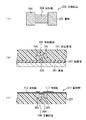
本願発明者は、従来のファンアウトWLPの技術を適用して部品内蔵基板を製造したときに所望の特性を安定して確保することが容易でない原因について検討を行った。この結果、図1(a)に示すように、受動部品506の電極505が活性部504よりも突出していることが特性に影響を及ぼしていることが判明した。例えば、受動部品506が十分に基板501上の粘着層502に貼り付けられておらず、図1(b)に示すように、封止の際に封止樹脂507から受ける応力により受動部品506が粘着層502から外れてしまうことがある。また、図1(c)に示すように、電極505と活性部504との間の段差に伴う凹凸が配線層514内の絶縁膜512及び導電膜513に反映され、導電膜513の屈曲した部分で断線が生じることがある。
The inventor of the present application has examined the cause that it is not easy to stably secure desired characteristics when a component-embedded substrate is manufactured by applying the conventional fan-out WLP technique. As a result, as shown in FIG. 1A, it has been found that the characteristics of the
本願発明者は、これらの知見に基づいて以下に示す諸態様に相当した。以下、実施形態について添付の図面を参照しながら具体的に説明する。 The inventors of the present application corresponded to various aspects shown below based on these findings. Hereinafter, embodiments will be described in detail with reference to the accompanying drawings.
(第1の実施形態)
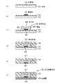
先ず、第1の実施形態について説明する。第1の実施形態は、部品内蔵基板の製造方法に関する。図2は、第1の実施形態に係る部品内蔵基板の製造方法を工程順に示す断面図であり、図3は、第1の実施形態に係る部品内蔵基板の製造方法を工程順に示す平面図である。
(First embodiment)
First, the first embodiment will be described. The first embodiment relates to a method for manufacturing a component-embedded substrate. FIG. 2 is a cross-sectional view illustrating the manufacturing method of the component built-in substrate according to the first embodiment in the order of steps, and FIG. 3 is a plan view illustrating the manufacturing method of the component built-in substrate according to the first embodiment in the order of steps. is there.
第1の実施形態では、先ず、図2(a)及び図3(a)に示すように、基板101上に粘着層102を形成する。次いで、図2(b)及び図3(b)に示すように、粘着層102の一部上に樹脂材103を設ける。その後、図2(c)及び図3(c)に示すように、複数の電極105を有する電子部品106を粘着層102に、樹脂材103が複数の電極105の間に位置するように貼り付ける。電子部品106には活性部104も含まれる。続いて、図2(d)及び図3(d)に示すように、電子部品106を封止樹脂107で封止する。次いで、図2(e)に示すように、電子部品106を封止樹脂107内に残しながら粘着層102の粘着力を低下させ、基板101を封止樹脂107から剥離する。その後、図2(f)に示すように、複数の電極105に接続される配線層を形成する。このようにして、部品内蔵基板100が得られる。
In the first embodiment, first, as shown in FIGS. 2A and 3A, the
そして、第1の実施形態により製造された部品内蔵基板100には、図2(f)に示すように、配線層108と、配線層108上の複数の電極105を有する電子部品106と、配線層108上で電子部品106を封止する封止樹脂107と、が含まれる。更に、電子部品106と配線層108との間、かつ複数の電極105間の樹脂材103も部品内蔵基板100に含まれる。この部品内蔵基板100では、電極105の配線層108と接する面と、樹脂材103の配線層108と接する面とが実質的に同一の平面内にある。
The component-embedded substrate 100 manufactured according to the first embodiment includes a wiring layer 108, an
このような第1の実施形態によれば、電子部品106の電極105と粘着層102との間に樹脂材103が存在するため、樹脂材103が設けられない場合と比較して、電子部品106と粘着層102との間の付着性を向上することができる。このため、封止の際に電子部品106を粘着層102上に安定して保持することができる。更に、粘着層102の除去後に、電極105の間に樹脂材103が残存しているため、配線層108は実質的に平坦な面上に形成される。従って、電子部品106の電極105が活性部104より突出していても、配線層108内の導電膜は電極105と活性部104との間の段差の影響を受けにくく、この段差に伴う断線を抑制することができる。
According to the first embodiment, since the
(第2の実施形態)
次に、第2の実施形態について説明する。第2の実施形態は、部品内蔵基板の製造方法に関する。図4A乃至図4Bは、第2の実施形態に係る部品内蔵基板の製造方法を工程順に示す断面図である。
(Second Embodiment)
Next, a second embodiment will be described. The second embodiment relates to a method for manufacturing a component-embedded substrate. 4A to 4B are cross-sectional views illustrating a method of manufacturing a component-embedded substrate according to the second embodiment in the order of steps.
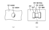
第2の実施形態では、先ず、図4A(a)に示すように、基板201上に粘着層202を形成する。基板201としては、例えばステンレス基板を用いる。粘着層202としては、例えば熱発泡フィルムを用いる。
In the second embodiment, first, an
次いで、図4A(b)に示すように、粘着層202の一部上に樹脂材203を設ける。例えば、エポキシ系樹脂、ポリイミド系樹脂又はアクリル系樹脂を樹脂材203として粘着層202上に滴下する。
Next, as shown in FIG. 4A (b), a
その後、図4A(c)に示すように、半導体チップ211を粘着層202に貼り付け、活性部204及び複数の電極205を有する電子部品206を粘着層202に、樹脂材203が複数の電極205の間に位置するように貼り付ける。半導体チップ211は能動部品の一例である。電子部品206は受動部品の一例であり、電子部品206としては、例えばチップコンデンサ等が用いられる。樹脂材203は、例えば、活性部204と電極205との間の段差の大きさよりも高くなるように滴下しておく。樹脂材203をこのように滴下しておくことにより、電子部品206を粘着層102に貼り付ける際に、樹脂材203が電子部品206と粘着層202との間、かつ複数の電極205間に広がる。樹脂材203の滴下量は、例えば電極205と粘着層202との間にまで樹脂材203が入り込まないように調整しておくことが好ましい。樹脂材203としてシリカフィラーを含有するエポキシ樹脂又はポリイミド樹脂を用いてもよい。この場合、樹脂材203中のシリカフィラーの粒径(直径)は、活性部204と電極205との間の段差の大きさよりも小さいものとする。
4A (c), the
続いて、図4A(d)に示すように、半導体チップ211及び電子部品206を封止樹脂107で封止する。封止の際には、例えば120℃で8分間の熱処理を行って封止樹脂107を熱硬化(キュア)させる。この熱処理の際に樹脂材203も熱硬化する。封止樹脂207としては、例えばシリカフィラーを含有するエポキシ樹脂又はポリイミド樹脂を用いる。封止樹脂207中のシリカフィラーの粒径は、活性部204と電極205との間の段差の大きさより大きくてもよい。電子部品206と粘着層202との間に納まる必要がないからである。一般的に、シリカフィラーの粒径が大きい樹脂ほど低コストで入手できる。
Subsequently, as shown in FIG. 4A (d), the
次いで、図4A(e)に示すように、基板201が上側になるように反転させ、図4B(f)に示すように、半導体チップ211及び電子部品206を封止樹脂207内に残しながら粘着層202の粘着力を低下させ、基板201を封止樹脂207から剥離する。例えばホットプレートを用いて180℃で2分間の熱処理を行うことにより、粘着層202の粘着力を低下させることができる。熱処理により粘着層202が発泡するため、粘着層202の粘着力が低下するのである。
Next, as shown in FIG. 4A (e), the
その後、図4B(g)に示すように、複数の電極205に接続される配線層214を形成する。配線層214の形成では、例えばセミアディティブ法により、絶縁膜212及び導電膜213を形成する。導電膜213の一部を電極205に接続する。
Thereafter, as shown in FIG. 4B (g), a
続いて、図4B(h)に示すように、配線層214上に配線層217を形成する。配線層217の形成では、例えばセミアディティブ法により、絶縁膜215及び導電膜216を形成する。導電膜216の一部を導電膜213に接続する。
Subsequently, as shown in FIG. 4B (h), a
次いで、図4B(i)に示すように、導電膜216のパッドとなる部分上に半田ボール218を形成する。その後、ダイシングを行う。このようにして、個片化された部品内蔵基板200が得られる。
Next, as shown in FIG. 4B (i), a solder ball 218 is formed on a portion to be a pad of the
そして、部品内蔵基板200は、例えば、図5に示すように、プリント基板220上に実装して用いられる。 The component-embedded substrate 200 is used by being mounted on a printed circuit board 220, for example, as shown in FIG.
このような第2の実施形態によれば、電子部品206の電極205と粘着層202との間に樹脂材203が存在するため、樹脂材203が設けられない場合と比較して、電子部品206と粘着層202との間の付着性を向上することができる。このため、封止の際に電子部品206を粘着層202上に安定して保持することができる。更に、粘着層202の除去後に、電極205の間に樹脂材203が残存しているため、配線層214は実質的に平坦な面上に形成される。従って、電子部品206の電極205が活性部204より突出していても、配線層214内の導電膜216は電極205と活性部204との間の段差の影響を受けにくく、この段差に伴う断線を抑制することができる。
According to the second embodiment, since the
(第3の実施形態)
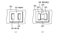
次に、第3の実施形態について説明する。第3の実施形態は、部品内蔵基板の製造方法に関する。図7は、第3の実施形態に係る部品内蔵基板の製造方法を工程順に示す断面図である。図8は、第3の実施形態に係る部品内蔵基板の製造方法を工程順に示す平面図である。
(Third embodiment)
Next, a third embodiment will be described. The third embodiment relates to a method for manufacturing a component-embedded substrate. FIG. 7 is a cross-sectional view showing the method of manufacturing the component-embedded substrate according to the third embodiment in the order of steps. FIG. 8 is a plan view illustrating the method for manufacturing the component-embedded substrate according to the third embodiment in the order of steps.
上記のように、第2の実施形態では、図4A(b)及び図6(a)に示すように、樹脂材203を粘着層202上に滴下した後に、図4A(c)及び図6(b)に示すように、樹脂材203を潰すようにして電子部品206を粘着層202に貼り付ける。第3の実施形態では、図7(a)及び図8(a)に示すように、複数の開口部304が形成されたシート状の樹脂材303を粘着層202上に設ける。次いで、図7(b)及び図8(b)に示すように、電子部品206の電極205を開口部304を通じて粘着層202に接触させる。そして、第3の実施形態と同様に、半導体チップ211及び電子部品206を封止樹脂107で封止する。封止の際には、例えば120℃で8分間の熱処理を行って封止樹脂107を熱硬化(キュア)させる。この熱処理の際に、樹脂材203が一旦流動化し、その後に熱硬化する。他の処理は第2の実施形態と同様である。
As described above, in the second embodiment, as shown in FIG. 4A (b) and FIG. 6 (a), after the
このような第3の実施形態によっても第2の実施形態と同様の効果を得ることができる。 The effect similar to 2nd Embodiment can be acquired also by such 3rd Embodiment.
樹脂材303の材料としては、例えばエポキシ系樹脂、ポリイミド系樹脂又はアクリル系樹脂が挙げられる。
Examples of the material of the
第2の実施形態及び第3の実施形態において、粘着層202は熱発泡フィルムに限定されない。例えば、加熱により粘着力が低下する材料、及び紫外線の照射により粘着力が低下する材料等を粘着層202に用いることができる。
In the second embodiment and the third embodiment, the
上記のように、樹脂材203中のシリカフィラーの粒径は、活性部204と電極205との間の段差の大きさよりも小さいものとすることが好ましく、封止樹脂207中のシリカフィラーの粒径は、活性部204と電極205との間の段差の大きさより大きくてもよい。また、シリカフィラーの粒径が大きい樹脂ほど低コストで入手できる。従って、封止樹脂207中のシリカフィラーの粒径は樹脂材203中のシリカフィラーの粒径より大きいことが好ましい。樹脂材303についても同様である。
As described above, the particle size of the silica filler in the
第2の実施形態及び第3の実施形態では、樹脂材203又は303の熱硬化(キュア)を封止樹脂207の熱硬化と共に行っているが、封止樹脂207の熱硬化の前に樹脂材203又は303を熱硬化させてもよい。
In the second and third embodiments, the thermosetting (curing) of the
また、部品内蔵基板に含まれる配線層の数は限定されない。第1の実施形態のように1層でもよく、第2の実施形態及び第3の実施形態のように2層でもよく、より多くの配線層が設けられていてもよい。 Further, the number of wiring layers included in the component built-in substrate is not limited. One layer may be used as in the first embodiment, two layers may be used as in the second and third embodiments, and more wiring layers may be provided.
以下、本発明の諸態様を付記としてまとめて記載する。 Hereinafter, various aspects of the present invention will be collectively described as supplementary notes.
(付記1)
基板上に粘着層を形成する工程と、
前記粘着層の一部上に樹脂材を設ける工程と、
複数の電極を有する電子部品を前記粘着層に前記樹脂材が前記複数の電極の間に位置するように貼り付ける工程と、
前記電子部品を封止樹脂で封止する工程と、
前記電子部品を前記封止樹脂内に残しながら前記粘着層の粘着力を低下させる工程と、
前記基板を前記封止樹脂から剥離する工程と、
前記複数の電極に接続される配線層を形成する工程と、
を有することを特徴とする部品内蔵基板の製造方法。
(Appendix 1)
Forming an adhesive layer on the substrate;
Providing a resin material on a part of the adhesive layer;
A step of attaching an electronic component having a plurality of electrodes to the adhesive layer so that the resin material is positioned between the plurality of electrodes;
Sealing the electronic component with a sealing resin;
Reducing the adhesive force of the adhesive layer while leaving the electronic component in the sealing resin;
Peeling the substrate from the sealing resin;
Forming a wiring layer connected to the plurality of electrodes;
A method of manufacturing a component-embedded substrate, comprising
(付記2)
前記粘着層として熱発泡フィルムを形成し、
前記粘着層の粘着力を低下させる工程は、前記熱発泡フィルムを加熱する工程を有することを特徴とする付記1に記載の部品内蔵基板の製造方法。
(Appendix 2)
Forming a thermally foamed film as the adhesive layer,
The method for manufacturing a component built-in substrate according to
(付記3)
前記電子部品は受動部品であることを特徴とする付記1又は2に記載の部品内蔵基板の製造方法。
(Appendix 3)
The method for manufacturing a component-embedded substrate according to
(付記4)
前記樹脂材を設ける工程は、前記樹脂材を前記粘着層の一部上に滴下する工程を有することを特徴とする付記1乃至3のいずれか1項に記載の部品内蔵基板の製造方法。
(Appendix 4)
4. The method for manufacturing a component-embedded substrate according to any one of
(付記5)
前記樹脂材を設ける工程は、複数の開口部が形成されたシート状の樹脂材を前記粘着層上に設ける工程を有し、
前記電子部品を前記粘着層に貼り付ける工程は、前記複数の電極を前記複数の開口部を通じて前記粘着層に接触させる工程を有することを特徴とする付記1乃至3のいずれか1項に記載の部品内蔵基板の製造方法。
(Appendix 5)
The step of providing the resin material includes a step of providing a sheet-like resin material having a plurality of openings formed on the adhesive layer,
4. The method according to
(付記6)
前記樹脂材は、第1の平均粒径のシリカフィラーを含有し、
前記封止樹脂は、前記第1の平均粒径よりも大きい第2の平均粒径のシリカフィラーを含有することを特徴とする付記1乃至5のいずれか1項に記載の部品内蔵基板の製造方法。
(Appendix 6)
The resin material contains a silica filler having a first average particle diameter,
6. The component built-in substrate according to any one of
(付記7)
配線層と、
前記配線層上の複数の電極を有する電子部品と、
前記配線層上で前記電子部品を封止する封止樹脂と、
前記電子部品と前記配線層との間、かつ前記複数の電極間の樹脂材と、
を有することを特徴とする部品内蔵基板。
(Appendix 7)
A wiring layer;
An electronic component having a plurality of electrodes on the wiring layer;
A sealing resin for sealing the electronic component on the wiring layer;
A resin material between the electronic component and the wiring layer, and between the plurality of electrodes,
A component-embedded substrate comprising:
(付記8)
前記複数の電極の前記配線層と接する面と、前記樹脂材の前記配線層と接する面とは実質的に同一の平面内にあることを特徴とする付記7に記載の部品内蔵基板。
(Appendix 8)
The component built-in substrate according to appendix 7, wherein a surface of the plurality of electrodes that contacts the wiring layer and a surface of the resin material that contacts the wiring layer are in substantially the same plane.
(付記9)
前記電子部品は受動部品であることを特徴とする付記7又は8に記載の部品内蔵基板。
(Appendix 9)
9. The component built-in substrate according to appendix 7 or 8, wherein the electronic component is a passive component.
(付記10)
前記樹脂材は、第1の平均粒径のシリカフィラーを含有し、
前記封止樹脂は、前記第1の平均粒径よりも大きい第2の平均粒径のシリカフィラーを含有することを特徴とする付記7乃至9のいずれか1項に記載の部品内蔵基板。
(Appendix 10)
The resin material contains a silica filler having a first average particle diameter,
10. The component built-in substrate according to any one of appendices 7 to 9, wherein the sealing resin contains a silica filler having a second average particle size larger than the first average particle size.
100、200:部品内蔵基板
101、201:基板
102、202:粘着層
103、203、303:樹脂材
104、204:活性部
105、205:電極
106、206:電子部品
107、207:封止樹脂
108、214、217:配線層
211:半導体チップ
213、216:導電膜
218:半田ボール
304:開口部
100, 200: Component built-in
Claims (5)
前記粘着層の一部上に樹脂材を設ける工程と、
複数の電極を有する電子部品を前記粘着層に前記樹脂材が前記基板の表面に平行な方向において前記複数の電極の間に位置するように貼り付ける工程と、
前記電子部品を封止樹脂で封止する工程と、
前記電子部品を前記封止樹脂内に残しながら前記粘着層の粘着力を低下させる工程と、
前記基板を前記封止樹脂から剥離する工程と、
前記複数の電極に接続される配線層を形成する工程と、
を有することを特徴とする部品内蔵基板の製造方法。 Forming an adhesive layer on the substrate;
Providing a resin material on a part of the adhesive layer;
A step of attaching an electronic component having a plurality of electrodes to the adhesive layer so that the resin material is positioned between the plurality of electrodes in a direction parallel to the surface of the substrate;
Sealing the electronic component with a sealing resin;
Reducing the adhesive force of the adhesive layer while leaving the electronic component in the sealing resin;
Peeling the substrate from the sealing resin;
Forming a wiring layer connected to the plurality of electrodes;
A method of manufacturing a component-embedded substrate, comprising
前記粘着層の粘着力を低下させる工程は、前記熱発泡フィルムを加熱する工程を有することを特徴とする請求項1に記載の部品内蔵基板の製造方法。 Forming a thermally foamed film as the adhesive layer,
The method of manufacturing a component built-in substrate according to claim 1, wherein the step of reducing the adhesive strength of the adhesive layer includes a step of heating the thermally foamed film.
前記電子部品を前記粘着層に貼り付ける工程は、前記複数の電極を前記複数の開口部を通じて前記粘着層に接触させる工程を有することを特徴とする請求項1乃至3のいずれか1項に記載の部品内蔵基板の製造方法。 The step of providing the resin material includes a step of providing a sheet-like resin material having a plurality of openings formed on the adhesive layer,
4. The method according to claim 1, wherein the step of attaching the electronic component to the adhesive layer includes a step of bringing the plurality of electrodes into contact with the adhesive layer through the plurality of openings. Manufacturing method of component built-in board.
Priority Applications (1)
| Application Number | Priority Date | Filing Date | Title |
|---|---|---|---|
| JP2014046745A JP6467775B2 (en) | 2014-03-10 | 2014-03-10 | Manufacturing method of component-embedded substrate |
Applications Claiming Priority (1)
| Application Number | Priority Date | Filing Date | Title |
|---|---|---|---|
| JP2014046745A JP6467775B2 (en) | 2014-03-10 | 2014-03-10 | Manufacturing method of component-embedded substrate |
Publications (2)
| Publication Number | Publication Date |
|---|---|
| JP2015170814A JP2015170814A (en) | 2015-09-28 |
| JP6467775B2 true JP6467775B2 (en) | 2019-02-13 |
Family
ID=54203255
Family Applications (1)
| Application Number | Title | Priority Date | Filing Date |
|---|---|---|---|
| JP2014046745A Expired - Fee Related JP6467775B2 (en) | 2014-03-10 | 2014-03-10 | Manufacturing method of component-embedded substrate |
Country Status (1)
| Country | Link |
|---|---|
| JP (1) | JP6467775B2 (en) |
Families Citing this family (4)
| Publication number | Priority date | Publication date | Assignee | Title |
|---|---|---|---|---|
| JP6597065B2 (en) | 2015-08-31 | 2019-10-30 | 株式会社デンソー | Silicon carbide single crystal, silicon carbide single crystal wafer, silicon carbide single crystal epitaxial wafer, electronic device |
| US10092396B2 (en) * | 2015-12-14 | 2018-10-09 | Novartis Ag | Flexible, hermetic electrical interconnect for electronic and optoelectronic devices for in vivo use |
| CN110572937B (en) * | 2018-06-06 | 2022-07-08 | 江西卓讯微电子有限公司 | Sensor with a sensor element |
| US20240112941A1 (en) * | 2019-10-17 | 2024-04-04 | Showa Denko Materials Co., Ltd. | Method for manufacturing electronic component device and electronic component device |
Family Cites Families (7)
| Publication number | Priority date | Publication date | Assignee | Title |
|---|---|---|---|---|
| JP3094481B2 (en) * | 1991-03-13 | 2000-10-03 | 松下電器産業株式会社 | Electronic circuit device and manufacturing method thereof |
| JPH08213747A (en) * | 1995-02-02 | 1996-08-20 | Fujitsu Ltd | Mounting method for surface mount components |
| JP2001320145A (en) * | 2000-05-10 | 2001-11-16 | Nec Corp | Method and structure for mounting electronic part |
| JP2004273853A (en) * | 2003-03-10 | 2004-09-30 | Matsushita Electric Ind Co Ltd | Chip component with resin layer, component built-in module using the same, and manufacturing method thereof |
| JP4158714B2 (en) * | 2004-02-06 | 2008-10-01 | 松下電器産業株式会社 | Method for manufacturing electronic component mounted substrate |
| JP2006173489A (en) * | 2004-12-17 | 2006-06-29 | Tokai Rika Co Ltd | Electronic component mounting structure |
| JP5870626B2 (en) * | 2011-11-01 | 2016-03-01 | 富士通株式会社 | Semiconductor device and manufacturing method of semiconductor device |
-
2014
- 2014-03-10 JP JP2014046745A patent/JP6467775B2/en not_active Expired - Fee Related
Also Published As
| Publication number | Publication date |
|---|---|
| JP2015170814A (en) | 2015-09-28 |
Similar Documents
| Publication | Publication Date | Title |
|---|---|---|
| JP5161732B2 (en) | Manufacturing method of semiconductor device | |
| US8138018B2 (en) | Manufacturing method of semiconductor device having underfill resin formed without void between semiconductor chip and wiring board | |
| US9214361B2 (en) | Semiconductor device manufacturing method and electronic device manufacturing method | |
| US20140042638A1 (en) | Semiconductor package and method of fabricating the same | |
| JP2017045867A (en) | Manufacturing method of component built-in wiring board, component built-in wiring board, and electronic component fixing tape | |
| US9136172B2 (en) | Method of manufacturing semiconductor device and method of manufacturing electronic assembly | |
| US20170245365A1 (en) | Printed wiring board and method for manufacturing the same | |
| WO2010070806A1 (en) | Semiconductor device, flip-chip mounting method and flip-chip mounting apparatus | |
| JP6467775B2 (en) | Manufacturing method of component-embedded substrate | |
| JP2015153811A (en) | Semiconductor device and manufacturing method of the same | |
| US11742310B2 (en) | Method of manufacturing semiconductor device | |
| TWI567888B (en) | Package structure and its manufacturing method | |
| JP2016025281A (en) | Semiconductor device and method for manufacturing the same | |
| CN102931095A (en) | Manufacturing method of package substrate and semiconductor package structure thereof | |
| JP2018041827A (en) | Component-embedded substrate and electronic device | |
| KR20160001827A (en) | Method for manufacturing a circuit board | |
| US9123700B2 (en) | Integrated circuit constructions having through substrate vias and methods of forming integrated circuit constructions having through substrate vias | |
| JP2006173234A (en) | Semiconductor device and manufacturing method thereof | |
| US8556159B2 (en) | Embedded electronic component | |
| JP6988360B2 (en) | Manufacturing method of semiconductor device and semiconductor device | |
| US20090309208A1 (en) | Semiconductor device and method of manufacturing the same | |
| TW201901821A (en) | Semiconductor device and method for manufacturing semiconductor device | |
| CN114930991A (en) | Method for conformally coating multiple rows of surface mount components in a lidless BGA package and products made thereby | |
| KR20130031486A (en) | Method for manufacturing semiconductor package | |
| JP2012186511A (en) | Semiconductor device manufacturing method |
Legal Events
| Date | Code | Title | Description |
|---|---|---|---|
| A621 | Written request for application examination |
Free format text: JAPANESE INTERMEDIATE CODE: A621 Effective date: 20161102 |
|
| A977 | Report on retrieval |
Free format text: JAPANESE INTERMEDIATE CODE: A971007 Effective date: 20170825 |
|
| A131 | Notification of reasons for refusal |
Free format text: JAPANESE INTERMEDIATE CODE: A131 Effective date: 20170912 |
|
| A521 | Request for written amendment filed |
Free format text: JAPANESE INTERMEDIATE CODE: A523 Effective date: 20171107 |
|
| A131 | Notification of reasons for refusal |
Free format text: JAPANESE INTERMEDIATE CODE: A131 Effective date: 20180522 |
|
| A521 | Request for written amendment filed |
Free format text: JAPANESE INTERMEDIATE CODE: A523 Effective date: 20180720 |
|
| TRDD | Decision of grant or rejection written | ||
| A01 | Written decision to grant a patent or to grant a registration (utility model) |
Free format text: JAPANESE INTERMEDIATE CODE: A01 Effective date: 20181218 |
|
| A61 | First payment of annual fees (during grant procedure) |
Free format text: JAPANESE INTERMEDIATE CODE: A61 Effective date: 20181231 |
|
| R150 | Certificate of patent or registration of utility model |
Ref document number: 6467775 Country of ref document: JP Free format text: JAPANESE INTERMEDIATE CODE: R150 |
|
| LAPS | Cancellation because of no payment of annual fees |