JP6433159B2 - Information processing apparatus, method, and program - Google Patents
Information processing apparatus, method, and program Download PDFInfo
- Publication number
- JP6433159B2 JP6433159B2 JP2014112746A JP2014112746A JP6433159B2 JP 6433159 B2 JP6433159 B2 JP 6433159B2 JP 2014112746 A JP2014112746 A JP 2014112746A JP 2014112746 A JP2014112746 A JP 2014112746A JP 6433159 B2 JP6433159 B2 JP 6433159B2
- Authority
- JP
- Japan
- Prior art keywords
- power supply
- die
- information
- package
- specified
- Prior art date
- Legal status (The legal status is an assumption and is not a legal conclusion. Google has not performed a legal analysis and makes no representation as to the accuracy of the status listed.)
- Active
Links
Images


Classifications
-
- G—PHYSICS
- G06—COMPUTING; CALCULATING OR COUNTING
- G06F—ELECTRIC DIGITAL DATA PROCESSING
- G06F30/00—Computer-aided design [CAD]
- G06F30/30—Circuit design
- G06F30/39—Circuit design at the physical level
- G06F30/398—Design verification or optimisation, e.g. using design rule check [DRC], layout versus schematics [LVS] or finite element methods [FEM]
Description
本発明は、ICの電源端子から発生するノイズをICのパッケージを考慮しプリント基板内で抑止するためのバイパスコンデンサの配置を検証する技術に関する。 The present invention relates to a technique for verifying the arrangement of a bypass capacitor for suppressing noise generated from a power supply terminal of an IC in a printed circuit board in consideration of an IC package.
集積回路(Integrated Circuit:IC)や大規模集積回路(Large-Scale Integration:LSI)の信号の高速化に伴い、同時スイッチングノイズが大きくなっている。同時スイッチングノイズが大きくなると、電源電圧が変動し、集積回路や大規模集積回路の誤動作や信号伝送不良が発生し、同時スイッチングノイズを基板外に伝搬させると放射ノイズ特性が悪化する。これら問題を回避する目的で、集積回路の電源端子近傍にバイパスコンデンサ(パスコン)を配置することが行なわれている。 Simultaneous switching noise has increased with the increase in signal speed of integrated circuits (ICs) and large-scale integrated circuits (LSIs). When the simultaneous switching noise increases, the power supply voltage fluctuates, and malfunctions and signal transmission failures occur in the integrated circuit and the large-scale integrated circuit. If the simultaneous switching noise is propagated outside the substrate, the radiation noise characteristics deteriorate. In order to avoid these problems, a bypass capacitor (pass capacitor) is arranged near the power supply terminal of the integrated circuit.
そして、パスコンを適切に配置するための技術として、特許文献1には、プリント基板の設計情報を基に、ICの電源端子からパスコンの電源端子までの配線距離が所定の配線長以上で配線されている場合、対策指示を表示するという技術が開示されている。
As a technique for appropriately arranging the bypass capacitors,
しかしながら、特許文献1の技術では、ICのパッケージ内配線が考慮されておらず、バイパスコンデンサの配置を精度良く検証することができなかった。
However, in the technique of
そこで、本発明は、プリント基板における適切なバイパスコンデンサの配置を精度良く把握することができるようにすることを目的とする。 In view of the above, an object of the present invention is to make it possible to accurately grasp an appropriate placement of a bypass capacitor on a printed circuit board.
本発明に係る情報処理装置は、プリント基板の設計情報から仮想的なダイの電源端子及びグラウンド端子を特定するダイ端子特定手段と、前記設計情報からプリント基板上に配置されたバイパスコンデンサを特定するバイパスコンデンサ特定手段と、前記設計情報、特定された前記ダイの電源端子及びグラウンド端子の情報、及び特定された前記バイパスコンデンサの情報に基づいて、特定された前記バイパスコンデンサの配置を評価するための評価値を導出する手段と、を備えたことを特徴とする。 An information processing apparatus according to the present invention specifies a die terminal specifying means for specifying a virtual die power supply terminal and a ground terminal from design information of a printed circuit board, and specifies a bypass capacitor disposed on the printed circuit board from the design information. A bypass capacitor specifying means; and for evaluating the arrangement of the specified bypass capacitor based on the design information, the specified power supply terminal and ground terminal information of the die, and the specified bypass capacitor information And means for deriving an evaluation value.
本発明によれば、プリント基板における適切なバイパスコンデンサの配置を精度良く把握することができる。 ADVANTAGE OF THE INVENTION According to this invention, arrangement | positioning of the appropriate bypass capacitor in a printed circuit board can be grasped | ascertained accurately.
以下、添付の図面を参照して、本発明を好適な実施例に基づいて詳細に説明する。なお、以下の実施例において示す構成は一例にすぎず、本発明は図示された構成に限定されるものではない。 Hereinafter, the present invention will be described in detail based on preferred embodiments with reference to the accompanying drawings. In addition, the structure shown in the following Examples is only an example, and this invention is not limited to the structure shown in figure.
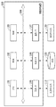
図1は、本実施例に係る、バイパスコンデンサ(以下、パスコン)の配置を検証する装置としてのPC等の情報処理装置の概略的構成を示す図である。情報処理装置100は、CPU101、ROM102、RAM103、システムバス104、入力I/F105、HDD I/F106、出力I/F107で構成される。
FIG. 1 is a diagram illustrating a schematic configuration of an information processing apparatus such as a PC as an apparatus for verifying the arrangement of bypass capacitors (hereinafter referred to as “pass capacitors”) according to the present embodiment. The
CPU101は、RAM103をワークメモリとして、ROM102及びハードディスクドライブ(HDD)120に格納されたプログラムを実行し、システムバス104を介して後述する各部を制御する。入力インタフェイス(I/F)105は、キーボードやマウスなどの入力デバイス110を接続する、例えばUSBやIEEE1394等のシリアルバスインタフェイスである。CPU101は、入力I/F105を介して入力デバイス110から各種データを読み込むことが可能である。HDDインタフェイス(I/F)106は、HDD120や光ディスクドライブなどの外部記憶装置を接続する、例えばシリアルATA(SATA)等のインタフェイスである。CPU101は、HDDI/F106を介して、HDD120からのデータ読み出し、およびHDD120へのデータ書き込みが可能である。さらにCPU101は、HDD120に格納されたデータをRAM103に展開し、同様に、RAM103に展開されたデータをHDD120に保存することが可能である。そしてCPU101は、RAM103に展開したデータをプログラムとみなし、実行することができる。出力インタフェイス(I/F)107は、液晶モニタ等の表示装置やプリンタといった出力デバイス130を接続する、例えばUSBやIEEE1394等のシリアルバスインタフェイスである。CPU101は、出力インタフェイス107を介して液晶モニタ等の表示装置に各種情報の表示を実行させ、或いは表示装置に出力された計算結果等の印刷をプリンタに実行させる。
The
HDD120内には、本発明を実施するためのプログラムや、プリント基板のレイアウトに関する設計情報(以下、設計情報)といった各種データが格納される。ここで、設計情報には、部品情報、配線情報、ドリル情報、層情報、パッケージ情報といった情報が含まれる。各情報の内容は以下のとおりである。
The
<部品情報>
・プリント基板上の部品の回路記号、位置座標、形状に関する情報
・部品の端子が接続される導電体部分の形状や信号名の情報
<Part information>
-Information on circuit symbols, position coordinates, and shapes of components on the printed circuit board-Information on the shape and signal name of the conductor part to which the component terminals are connected
<配線情報>
・部品間配線の信号名の情報
・配線図形を構成する各点の位置座標の情報
・回路記号、端子番号、信号名を用いて特定される、回路上の論理的な接続関係を表現するネットリストの情報
<Wiring information>
・ Signal name information for wiring between parts ・ Position coordinate information of each point constituting the wiring figure ・ Net expressing the logical connection relation on the circuit specified by circuit symbol, terminal number and signal name List information
<ドリル情報>
・ドリル孔の位置座標や形状等の情報
<Drill information>
・ Information such as drill hole position coordinates and shape
<層情報>
・プリント基板の層構成に関する情報
<Layer information>
・ Information on layer structure of printed circuit board
<パッケージ情報>
・ダイの端子やパッケージの端子の位置座標の情報
・ダイやパッケージの端子間配線の信号名の情報
・配線図形を構成する各点の位置座標の情報
・ダイやパッケージの端子の論理的な接続関係を表現するネットリストの情報
<Package information>
-Information on the position coordinates of the terminals of the die and package-Information on the signal names of the wiring between the terminals of the die and package-Information on the position coordinates of each point constituting the wiring figure-Logical connection of the terminals of the die and package Netlist information expressing relationships
図2は、本実施例に係る、パスコン配置を検証する装置としての情報処理装置100のソフトウェア構成を示す機能ブロック図である。本実施例に係る情報処理装置100は、設計情報管理部210、条件設定部220、検証部230及び検証結果出力部240で構成される。
FIG. 2 is a functional block diagram illustrating a software configuration of the
設計情報管理部210は、ユーザが入力デバイス110を用いて入力した設計情報を管理する。設計情報管理部210は、ユーザからの検証実行の指示を受けて、設計情報を検証部230へ送る。
The design
条件設定部220は、入力デバイス110を介したユーザ入力に従って、パスコン配置の検証処理を実行する際の検証条件を設定する。設定された検証条件は、検証部230へ送られる。
The
検証部230は、設計情報管理部210から受け取った設計情報を用いて、条件設定部220で設定された検証条件に従って、パスコン配置が適切かどうかを検証する処理を行う。本実施例における検証部230は、ダイ端子特定部231、パスコン特定部232、評価値導出部233、条件違反判定部234で構成される。
The
ダイ端子特定部231は、入力された設計情報に基づいて、ダイに関する電源とグラウンドの端子を特定する。特定されたダイの電源端子及びグラウンド端子の情報はRAM103に記憶される。なお、ユーザが入力デバイス110を用いて直接入力したダイの電源端子及びグラウンド端子の情報に基づいて、特定してもよい。
The die
バイパスコンデンサ特定部(パスコン特定部)232は、入力された設計情報とダイ端子特定部231で特定したダイの電源端子及びグラウンド端子の情報に基づいて、プリント基板上のパスコンを特定する。特定されたパスコンの情報はRAM103に記憶される。
The bypass capacitor specifying unit (pass capacitor specifying unit) 232 specifies a bypass capacitor on the printed circuit board based on the input design information and information on the power supply terminal and ground terminal of the die specified by the die
評価値導出部233は、入力された設計情報、特定されたダイの電源端子とグラウンド端子の情報、特定されたパスコンの情報に基づいて、パスコンの配置を評価するための評価値を導出する。本実施例では、ダイの電源端子からパスコンを経由してダイのグラウンド端子に至る経路の長さを評価値として導出する。
The evaluation
条件違反判定部234は、評価値導出部233で導出された評価値が検証条件に合致しているかどうかを判定する。判定の結果(検証結果)は、RAM103に記憶される。
The condition
検証結果出力部240は、検証結果に基づいて表示装置上に警告を表示したり、プリンタから検証結果をプリント出力したり、或いは不図示のネットワークI/Fを介して検証結果のデータを送信するなどして、検出結果をユーザに報知する。
The verification
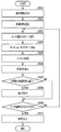
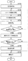
図3は、本実施例に係る、パスコン配置検証処理の流れを示すフローチャートである。この一連の処理は、CPU101が、ROM102に格納されているプログラムをRAM103にロードし、実行することで実現される。また、以下の説明においては、プリント基板及びICのパッケージの概略図である図4を適宜参照するものとする。なお、実際のプリント基板およびICのパッケージは、配線が高密度化・複雑化しているが以下の概略的説明はそれを排除するものではない。
FIG. 3 is a flowchart showing the flow of bypass capacitor arrangement verification processing according to the present embodiment. This series of processing is realized by the
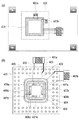
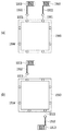
図3のフローの説明に入る前に、図4に示すプリント基板とICのパッケージについて説明する。図4(a)は、レイアウト設計完了段階における、パスコン401a及び401bが接続されたIC400を含むプリント基板のレイアウトを示す模式図である。図4(b)は、図4(a)内の破線で示す領域402の拡大図である。図4(b)において、403はプリント基板上の電源配線であり、404はプリント基板上のグラウンド配線である。405はパッケージ内の電源配線であり、406はパッケージ内のグラウンド配線である。407a〜407dはダイの電源端子であり、408a〜408dはダイのグラウンド端子である。409はパッケージ内の電源リングであり、410はパッケージ内のグラウンドリングである。
Prior to the description of the flow of FIG. 3, the printed circuit board and IC package shown in FIG. 4 will be described. FIG. 4A is a schematic diagram showing a layout of a printed circuit board including the
続いて、図3のフローチャートについて詳しく説明する。 Next, the flowchart of FIG. 3 will be described in detail.
ステップ301において、設計情報管理部210は、検証処理の対象となる、レイアウト設計完了段階の設計情報を検証部230へ送る。
In
ステップ302において 検証条件設定部220は、入力デバイス110を介して入力された内容に従って検証条件を設定する。ここで検証条件とは、上記設計情報で特定されるパスコンの配置が適切かどうかを判定するための条件である。本実施例では、ダイの電源端子からパスコンを経由してダイのグラウンド端子に至る経路の長さを評価値とした場合における、許容される経路長を表す閾値(以下、許容値)を指す。
In step 302, the verification
ステップ303において、検証部230内のダイ端子特定部231は、取得した設計情報を用いてダイの電源端子(以下、ダイVT又はピン)を1つ特定する。最初のルーチンで例えば、設計情報内のパッケージ情報に含まれる、ダイの端子を表す情報と電源を表す信号名とによって、ダイVT407aが特定される。そして、2回目以降のルーチンにおいて、他のダイVT407b〜407dも順次特定されることになる(図4を参照)。特定されたダイVTの情報は、RAM103に記憶される。
In step 303, the die
ステップ304において、検証部230内のダイ端子特定部231は、取得した設計情報を用いてダイのグラウンド端子(以下、ダイGT)をすべて特定する。例えば、設計情報内のパッケージ情報に含まれる、ダイの端子を表す情報とグラウンドを表す信号名とによって、ダイGT408a〜408dが特定される(図4を参照)。特定されたすべてのダイGTの情報は、RAM103に記憶される。
In
ステップ305において、検証部230内のパスコン特定部232は、ステップ303で特定されたダイVTとステップ304で特定されたダイGTとに接続するプリント基板上のコンデンサをパスコンとして特定する。図4の例では、ダイVT407aと同電位の電源配線403と、ダイGT408a〜408bと同電位のグラウンド配線404とに接続するコンデンサ401a及び401bが、パスコンとして特定されることになる。特定されたコンデンサ(パスコン)の情報は、RAM103に記憶される。
In
ステップ306において、検証部230内の評価値導出部233は、ステップ303で特定されたダイVTから、ステップ305で特定されたパスコンを経由し、ステップ304で特定された各ダイGTへと至る経路の長さを評価値として導出する。特定されたパスコンが複数存在する場合にはそれぞれのパスコンについて、この評価値導出処理がなされる。例えば、図4におけるパスコン401aの場合、始点をダイVT407a、終点をパスコン401aの電源側端子とした、面図形による最短経路探索をまず実施する。さらに、パスコン401aのグラウンド側端子を始点とし、ダイGT408a〜408dをそれぞれ終点として最短経路探索を実施する。そして、上記2種類の最短経路探索によって得られた経路を足した長さ(以下、ループ距離)を求める。パスコン401aについては、以下の4パターンのループ距離が求められることになる。
In step 306, the evaluation
1)「ダイVT407a〜パスコン401aの電源側端子」+「パスコン401aのグラウンド側端子〜ダイGT408a」
2)「ダイVT407a〜パスコン401aの電源側端子」+「パスコン401aのグラウンド側端子〜ダイGT408b」
3)「ダイVT407a〜パスコン401aの電源側端子」+「パスコン401aのグラウンド側端子〜ダイGT408c」
4)「ダイVT407a〜パスコン401aの電源側端子」+「パスコン401aのグラウンド側端子〜ダイGT408d」
導出されたループ距離は、評価値としてRAM103に記憶される。
1) “Die VT407a to power supply side terminal of
2) “Die VT407a to power supply side terminal of
3) “Die VT407a to power supply side terminal of
4) “Die VT407a to power supply side terminal of
The derived loop distance is stored in the
ステップ307において、検証部230内の条件違反判定部234は、導出された評価値(ループ距離)と、ステップ302で設定された検証条件(許容値としてのループ距離)とを比較し、評価値が検証条件に合致するかどうかをパスコン毎に判定する。この場合において、各パスコンについて導出された全評価値のうち、最も評価が高いもの(ここではループ距離が最も短いもの)についてこの判定がなされる。導出された評価値(ループ距離)が、許容値として設定されたループ距離(例えば13mm)よりも長い場合は、検証条件に違反すると判定し、ステップ308へ進む。一方、導出された評価値(ループ距離)が許容値として設定されたループ距離以下の場合は、検証条件に合致すると判定し、ステップ309へ進む。
In step 307, the condition
ステップ308において、検証部230内の条件違反判定部234は、検証条件に違反していることを示す情報(以下、違反情報)をRAM103に記憶する。この違反情報は、例えば、ICの回路記号及び端子名、パスコンの回路記号や座標、電源配線及びグラウンド配線の信号名などで構成される。
In
ステップ309において、検証部230は、すべてのダイVTが特定されたかどうかを判定する。未特定のダイVTがある場合はステップ303に戻って次のダイVTを1つ特定して、ステップ304〜308の各処理を繰り返す。一方、全てのダイVTが特定されている場合は、ステップ310へ進む。
In
ステップ310において、検証結果出力部240は、出力デバイス130に検証結果を出力する。具体的には、表示装置に検証結果を表示したり、プリンタで検証結果を印刷したりする。或いは、検証結果を記述したファイルをHDD120に格納したり、不図示のネットワークを介して他のPC等に送信してもよい。図5は、本実施例における検証結果出力の一例を示す図である。図5(a)は、パスコン401a及び401bのうち、パスコン401bの評価値が検証条件に合致しないと判定された場合の結果を視覚的に示した場合の一例である。ここでは、設定された検証条件(許容値)が13mmであったのに対し、導出されたループ距離が例えば15mmであったため、レイアウト画面上に違反であったことを表す×印の記号500が示されている。また、図5(b)は、同様の検証結果を以下の項目からなる表形式で示した一例である。
In
・ICの回路記号、端子名、信号名
・パスコンの回路記号、座標、実装面
・導出された評価値(ループ距離)とそれに対する判定結果
図5(b)の場合において、例えば表示装置に表示された表上のパスコンの回路記号等をユーザが入力デバイス110を用いて選択すると、選択したパスコンがレイアウト画面上でハイライトやズーム、ポップアップ画面等によって強調表示されるようにしてもよい。なお、表形式で検証結果を出力する場合にあっては、上記ステップ303及び304で特定されたダイVTやダイGTの端子名に対応するパッケージ側の端子名を、ダイVTやダイGTの端子名に代えて用いてもよいし、或いはこれを併記してもよい。
・ IC circuit symbol, terminal name, signal name ・ Circuit capacitor circuit symbol, coordinates, mounting surface ・ Derived evaluation value (loop distance) and its determination result In the case of FIG. When the user selects a circuit symbol of a bypass capacitor on the displayed table using the
以上が、本実施例に係る、パスコンの配置を検証する処理の内容である。 The above is the content of the process for verifying the layout of the bypass capacitors according to the present embodiment.
上述のステップ303及び304では、取得した設計情報からダイVT及びダイGTの実際の位置を特定したが、設計情報に基づいてダイVT及びダイGTの仮想的な位置を特定してもよい。図6は、仮想的なダイVT及びダイGTを特定する方法を説明する図である。図6において、例えば、パッケージの電源配線405と電源リング409とが接続する接続点600を仮想的なダイVTとして特定することが考えられる。さらに、IC400の中心座標602を仮想的なダイVTとして特定してもよい。仮想的なダイGTも、仮想的なダイVTの特定と同様、パッケージの電源配線406とグラウンドリング410とが接続する接続点601やIC400の中心座標602を仮想的なダイGTとして特定してもよい。このように仮想的に電源端子やグラウンド端子を特定することで、処理全体を簡略化することができる。
In
また、本実施例では、評価値としてのループ距離を一度の処理で導出している。しかし、パッケージの設計情報とプリント基板の設計情報が同一のCADに存在しない場合も考えられる。このような場合は、それぞれ別に経路を計算してから評価値としてのループ距離を導出すればよい。 In this embodiment, the loop distance as the evaluation value is derived by a single process. However, there may be a case where the package design information and the printed circuit board design information do not exist in the same CAD. In such a case, it is only necessary to derive a loop distance as an evaluation value after calculating a route separately.
さらに、ループ距離の代わりにインダクタンスを求めて、これを評価値としてもよい。この場合、検証条件としては、所定のインダクタンスを表す値が許容値として設定されることになる。 Furthermore, instead of the loop distance, an inductance may be obtained and used as an evaluation value. In this case, as a verification condition, a value representing a predetermined inductance is set as an allowable value.
また、本実施例では、評価値としてループ距離を算出しているが、経路が存在しない場合も考えられる。このような場合は、経路が算出されないといった違反情報を検証結果として表示することでユーザに報知すればよい。 In the present embodiment, the loop distance is calculated as the evaluation value, but there may be a case where there is no route. In such a case, what is necessary is just to alert | report to a user by displaying violation information that a path | route is not calculated as a verification result.
以上のとおり本実施によれば、ICのパッケージ内の配線を考慮してパスコン配置が適切なものであるかどうかを検証することができる。その結果、精度よくパスコンの配置を決定することが可能となる。 As described above, according to the present embodiment, it is possible to verify whether the bypass capacitor arrangement is appropriate in consideration of the wiring in the IC package. As a result, it is possible to accurately determine the location of the bypass capacitors.
実施例1は、レイアウト設計の完了後に、ICのパッケージ内の配線を考慮してパスコンの配置を検証する態様であった。次に、レイアウト設計段階でパスコン配置を検証する態様について、実施例2として説明する。なお、実施例1と共通する部分については説明を省略ないしは簡略化し、以下では差異点を中心に説明するものとする。 In the first embodiment, after the layout design is completed, the layout of the bypass capacitors is verified in consideration of the wiring in the IC package. Next, a mode for verifying the bypass capacitor arrangement at the layout design stage will be described as a second embodiment. The description of the parts common to the first embodiment will be omitted or simplified, and the differences will be mainly described below.
図7は、本実施例に係る、パスコン配置を検証する装置としての情報処理装置100のソフトウェア構成を示す機能ブロック図である。本実施例に係る情報処理装置100は、設計情報管理部210、検証部700及び検証結果出力部240で構成される。
FIG. 7 is a functional block diagram illustrating a software configuration of the
設計情報管理部210及び検証結果出力部240は、実施例1と同じである。以下、本実施例の特徴である検証部700について説明する。
The design
検証部700は、ダイ端子特定部701、パッケージ端子特定部702、評価値導出部703、優先順位設定部704で構成される。
The
ダイ端子特定部701は、入力された設計情報に基づいて、ダイの電源端子(ダイVT)を特定する。特定されたダイVTの情報はRAM103に記憶される。
The die
パッケージ端子特定部702は、入力された設計情報に基づいて、パッケージの電源端子(以下、パッケージVT)を特定する。特定されたパッケージVTの情報はRAM103に記憶される。なお、ユーザが入力デバイス110を用いて入力した、パッケージの電源端子を指定する情報に基づいて、特定してもよい。
The package terminal specifying unit 702 specifies a power supply terminal (hereinafter, package VT) of the package based on the inputted design information. Information on the identified package VT is stored in the
評価値導出部703は、入力された設計情報、特定されたダイVTの情報、特定されたパッケージVTの情報に基づいて、パスコンの配置を評価するための評価値を導出する。本実施例では、パッケージ内の経路長(ダイVTからパッケージVTまでの経路の長さ)を評価値として導出する。
The evaluation
優先順位設定部704は、評価値導出部703で導出した評価値に基づいて、特定されたパッケージVTについて優先順位を設定する。ここで優先順位とは、同電位のパッケージVTの中での、パスコンを接続することが望ましい優先度を示す順位であり、パッケージ内の経路が短いほど高い優先順位とする。パッケージ内の経路が短いパッケージVTの優先順位を高くする理由を、シミュレーション結果を用いて説明する。図8は、シミュレーションモデルを示す図であり、(a)はパッケージ内の経路が短いモデル、(b)はパッケージ内の経路が長いモデルである。図8(a)は、電源リング800と、それに接続するパッケージ内配線801、プリント基板上の配線802及びパスコン803で構成されている。図8(b)も同様に、電源リング810と、それに接続するパッケージ内配線811、プリント基板上の配線812及びパスコン813で構成されている。そして、図8(a)におけるパッケージ内配線801の長さは、同(b)におけるパッケージ内配線811に比べ短くなっている。この2つのモデルにおいて、点804及び814で示される計測点におけるインピーダンスをそれぞれ計測する。図9(a)は、両モデルにおけるインピーダンスの計測結果を示すグラフであり、実線はパッケージ内の経路が短いモデルに対応し、破線はパッケージ内の経路が長いモデルに対応している。そして、図9(b)は、1GHz(1000MHz)以下の周波数部分を拡大したものである。1GHz(1000MHz)以下の周波数に着目すると、パッケージ内の配線長が短いモデルの方がインピーダンスが低くなっているのが分かる(図9(b))。ICに安定的に電源を供給するには、電源リングからパスコンまでのインピーダンスを低くすることが重要であることが分かっている。そこで、電源リングからのインピーダンスがより低いパッケージVTにパスコンが接続されるように、パッケージ内の経路が短いパッケージVTに対し、高い優先順位を設定している。設定された優先順位は、検証結果としてRAM103に記憶される。
The priority
検証結果出力部240は、優先順位設定部704で設定された優先順位を、表示装置上に表示したり、プリンタからプリント出力したり、或いは不図示のネットワークI/Fを介して検証結果のデータを送信するなどして、検出結果としてユーザに報知する。
The verification
図10は、本実施例に係る、パスコン配置検証処理の流れを示すフローチャートである。この一連の処理は、CPU101が、ROM102に格納されているプログラムをRAM103にロードし、実行することで実現される。
FIG. 10 is a flowchart showing the flow of bypass capacitor arrangement verification processing according to the present embodiment. This series of processing is realized by the
ステップ1001において、設計情報管理部210は、検証処理の対象となるレイアウト設計段階の設計情報を検証部700へ送る。
In
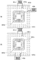
ステップ1002において、検証部700内のパッケージ端子特定部702は、取得した設計情報を用いてパッケージVTを1つ特定する。図11は、レイアウト設計段階におけるIC400のレイアウトを示す模式図である。この場合、最初のルーチンで例えば、パッケージ内電源配線405に接続するパッケージVT1101aが特定される。そして、2回目以降のルーチンにおいて、他のパッケージVT1101b〜1101dも順次特定されることになる。或いは、設計情報内のプリント基板のレイアウトに関する情報から、プリント基板上の電源配線に接続されているICのパッケージVTを特定してもよい。特定されたパッケージVTの情報は、RAM103に記憶される。
In step 1002, the package terminal identification unit 702 in the
ステップ1003において、検証部700内のダイ端子特定部701は、取得した設計情報を用いてダイVTをすべて特定する。例えば、設計情報内のICのパッケージ情報に含まれる、ダイの端子を表す情報と電源を表す信号名とによって、ダイVT407a〜407dが特定される(図11を参照)。特定されたダイVTの情報は、RAM103に記憶される。
In step 1003, the die
ステップ1004において、検証部700内の評価値導出部703は、ステップ1002で特定されたパッケージVTから、ステップ1003で特定された各ダイVTに至る経路の長さを導出する。導出された経路長は、評価値としてRAM103に記憶される。
In step 1004, the evaluation
ステップ1005において、検証部700は、未だ特定されていないパッケージVTがあるかどうかを判定する。未だ特定されていないパッケージVTがある場合はステップ1002に戻って次のパッケージVTを特定して、ステップ1003〜1005の処理を繰り返す。一方、全てのパッケージVTが特定されている場合は、ステップ1006へ進む。
In
ステップ1006において、検証部700内の優先順位設定部704は、特定されたすべてのパッケージVTについて、パスコンに接続する場合の優先順位を設定する。具体的には、まず信号名(プリント基板の電源の種類を表す信号名)が同じ電源配線に接続されているパッケージVTをグループ化する。図11の例では、4つのパッケージVT1101a〜1101dがグループ化される。そして、グループ化されたパッケージVTの中から、ステップ1004で導出したパッケージ内経路長が短い順に、高い優先順位を設定する。図11の場合、導出される経路長は短い順に以下のようになる。
In
・パッケージVT1101a〜ダイVT407aの経路
・パッケージVT1101b〜ダイVT407cの経路
・パッケージVT1101c〜ダイVT407dの経路
・パッケージVT1101d〜ダイVT407bの経路
したがって、優先順位が高い方から順に、1101a、1101b、1101c、1101dとなる。このようにして決定された優先順位の情報は、RAM103に記憶される。
・ Route of package VT1101a to die VT407a ・ Route of package VT1101b to die VT407c ・ Route of package VT1101c to die VT407d ・ Route of package VT1101d to die VT407b Become. The priority order information determined in this way is stored in the
ステップ1007において、検証結果出力部240は、出力デバイス130に検証結果としての優先順位を出力する。具体的には、表示装置に検証結果を表示したり、プリンタで検証結果を印刷したりする。或いは、検証結果を記述したファイルをHDD120に格納したり、不図示のネットワークを介して他のPC等に送信してもよい。図12は、本実施例における検証結果出力の一例を示す図である。図12(a)は、パッケージVT1101a〜1101dに対して設定された優先順位を視覚的に示した場合の一例であり、レイアウト画面上に優先順位が数字で表示されている。さらに、色分け等を組み合わせる等して、優先順位に応じた強調表示を行ってもよい。また、図12(b)は、ICの回路記号や端子名や信号名と共に、対応する優先順位を表形式で示した一例を示している。この場合において、例えば表示装置に表示された表上のパスコンの回路記号等をユーザが入力デバイス110を用いて選択すると、選択したパスコンがレイアウト画面上でハイライトやズーム、ポップアップ画面等によって強調表示されるようにしてもよい。
In
以上が、本実施例に係る、パスコンの配置を検証する処理の内容である。 The above is the content of the process for verifying the layout of the bypass capacitors according to the present embodiment.
なお、優先順位の他の決定方法として、接続可能な全てのダイVTまでの経路長を導出して合算し、合算結果(総経路長)が短いパッケージVTから順に高い優先順位を設定するようにしてもよい。 As another method for determining the priority order, the route lengths to all connectable dies VT are derived and added, and the higher priority is set in order from the package VT having the shortest result (total route length). May be.
また、本実施例では、最短経路の長さを評価値としたが、例えば、最短経路の長さの代わりにインダクタンスを求めて、これを評価値としてもよい。この場合、経路のインダクタンスが小さいほど高い優先順位を設定するようにすればよい。 In this embodiment, the length of the shortest path is used as the evaluation value. For example, instead of the length of the shortest path, an inductance may be obtained and used as the evaluation value. In this case, a higher priority may be set as the inductance of the path is smaller.
<実施例2の変形例>
さらに、レイアウト完了段階(パスコンが既に配置されている状態)において、上述のようにして設定された優先順位を用いて、配置の妥当性を判定し、その判定結果を出力してもよい。具体的には、ステップ1006で優先順位を設定した後、設計情報に基づいてパスコンを特定し、特定されたパスコンが接続しているパッケージVTの優先順位が高いかどうかを判定して、その判定結果も含め検証結果として出力する。図13は、この変形例に係る検証結果出力の一例を示す図である。図13においてパスコン401bは、優先順位が一番低いパッケージVT1101dに接続されている。図13(a)では、パスコン401bの配置が不適切であることを示す×印マーク1300に加え、より優先順位の高い他の電源端子(パッケージVT1101b)への接続を促すメッセージ1301がレイアウト画面上に表示された様子が示されている。また、表形式の出力例である図13(b)では、ICの回路記号や端子名や信号名、パスコンの回路記号、設定された優先順位に加えて、備考欄に上記メッセージ1301と同内容のコメントが表示されている。
<Modification of Example 2>
Further, in the layout completion stage (a state where the bypass capacitors are already arranged), the validity of the arrangement may be determined using the priority order set as described above, and the determination result may be output. Specifically, after setting the priority in
また、レイアウト設計の部品配置段階において、上述のようにして設定された優先順位を用いて、パスコンを自動配置してもよい。具体的には、ステップ1006で優先順位を設定した後、設計情報に基づいてパスコンを特定し、特定されたパスコンが接続している優先順位が高いパッケージVTの近傍へパスコンを配置する。
Further, at the part placement stage of the layout design, the bypass capacitors may be automatically placed using the priority order set as described above. Specifically, after setting the priority order in
本実施例によれば、レイアウト設計段階で(或いはレイアウト完了後に)、パスコンを配置するのに適したパッケージの電源端子を容易に把握でき、効率よくパスコンを配置することが可能となる。 According to the present embodiment, at the layout design stage (or after completion of the layout), it is possible to easily grasp the power supply terminals of the package suitable for arranging the bypass capacitors, and to efficiently arrange the bypass capacitors.
次に、複数のパスコンが密集しないよう分散配置を可能にする態様について、実施例3として説明する。なお、実施例1及び2と共通する部分については説明を省略ないしは簡略化し、以下では差異点を中心に説明するものとする。 Next, an embodiment that enables a distributed arrangement so that a plurality of decaps are not crowded will be described as a third embodiment. Note that description of parts common to the first and second embodiments will be omitted or simplified, and the following description will focus on differences.
図14は、本実施例に係る、パスコン配置を検証する装置としての情報処理装置100のソフトウェア構成を示す機能ブロック図である。本実施例に係る情報処理装置100は、設計情報管理部210、検証部1400及び検証結果出力部240で構成される。
FIG. 14 is a functional block diagram illustrating a software configuration of the
設計情報管理部210及び検証結果出力部240は実施例1及び2と同じであるため、説明を省く。
Since the design
検証部1400は、ダイ端子特定部701、パッケージ端子特定部702、評価値導出部703、優先順位設定部1401及び再配置部1402で構成される。なお、再配置部1402が破線で示されているのは、入力された設計情報がレイアウト設計の完了段階であった場合にのみ機能するためである。
The
ダイ端子特定部701、パッケージ端子特定部702及び評価値導出部703は、実施例2と同じである。
The die
優先順位設定部1401は、実施例2に係る優先順位設定部704と同様、評価値導出部703で導出した評価値に基づいてパッケージVTについての優先順位を設定する。これに加え、本実施例に係る優先順位設定部1401は、高い優先順位が設定されたパッケージVTが所定範囲内に密集している場合に、密集状態が解消するように優先順位を変更する処理も行なう。ここで、密集状態が解消するようにパッケージVTの優先順位を変更する理由を、シミュレーション結果を用いて説明する。図15は、シミュレーションモデルを示す図であり、(a)はパスコンが密集しているモデル、(b)はパスコンが分散しているモデルである。図15(a)は、電源リング1500と、それに接続するパッケージ内配線1501、プリント基板上の配線1502及び互いに近接して配置された2つのパスコン1503で構成されている。図15(b)も同様に、電源リング1510と、それに接続するパッケージ内配線1511、プリント基板上の配線1512及び一定距離を保って配置されている2つのパスコン1513で構成されている。図15(a)と図15(b)とでパッケージ内配線長やプリント基板上の配線長等の条件は同じであり、2つのパスコンの位置関係のみが異なっているものとする。この2つのモデルにおいて、点1504及び1514で示される計測点におけるインピーダンスをそれぞれ計測する。図16(a)は、両モデルにおけるインピーダンスの計測結果を示すグラフであり、実線はパスコンが密集しているモデルに対応し、破線はパスコンが分散しているモデルに対応している。そして、図16b)は、1GHz(1000MHz)以下の周波数部分を拡大したものである。1GHz(1000MHz)以下の周波数に着目すると、パスコンが分散しているモデルの方が、インピーダンスが低くなっているのが分かる(図16(b))。前述のとおり、ICへの電源の安定供給には、電源リングからパスコンまでのインピーダンスが低い方がよいので、電源リングに対してパスコンができるだけ分散して配置されるように優先順位を変更している。設定(変更)された優先順位は、検証結果としてRAM103に記憶される。
Similar to the
再配置部1402は、レイアウト設計の完了段階において、パッケージ端子特定部702で特定されたパッケージVTが互いに近接し過ぎていた場合に、変更後の優先順位に従って、パッケージVTが分散するようにパスコンを再配置する。
When the package VT specified by the package terminal specifying unit 702 is too close to each other at the stage of completing the layout design, the
図17は、本実施例に係る、パスコン配置検証処理の流れを示すフローチャートである。この一連の処理は、CPU101が、ROM102に格納されているプログラムをRAM103にロードし、実行することで実現される。
FIG. 17 is a flowchart illustrating a flow of bypass capacitor arrangement verification processing according to the present embodiment. This series of processing is realized by the
ステップ1701〜1706は、実施例2の図10のフローチャートにおけるステップ1001〜1006にそれぞれ対応するため、以下では、ステップ1707以降について詳しく説明する。
Steps 1701 to 1706 respectively correspond to
ステップ1706で優先順位が設定されると、ステップ1707において、優先順位設定部1401は、設計情報内のパッケージ情報に基づいて、特定された同電位のパッケージVTが一定距離を保って互いに離れているかどうかを判定する。図18は、同電位にある複数のパッケージVTが一定距離を保って離れているかどうかの判定手法の一例を説明する図である。図18の例では、同電位のパッケージ電源端子として4つのパッケージVT1801a〜1801dが特定され、それぞれの優先順位は高い順に、1801a、1801b、1801c、1801dとなっている。この場合において、まず、パッケージVT1801a〜1801dのそれぞれについて、パッケージ内の電源配線と電源リング409との接続点を中心とした両矢印で示される所定の範囲1802a〜1802dを特定する。そして、各パッケージVTに対する所定範囲1802a〜1802dが重なっている箇所がないかどうかを判定し、重なっている箇所があれば、当該箇所を密集箇所として特定する。図18の例では、優先順位が1位のパッケージVT1801aについての所定範囲1802aと優先順位が2位のパッケージVT1801bについての所定範囲1802bとの間で重なりがある(破線の丸で囲まれた部分)。そのため、パッケージVT1801a及びパッケージVT1801bの配置されている箇所が、密集箇所として特定されることになる。また、より簡易的な判定方法として、特定されたパッケージVT同士の間を結ぶ直線距離を求め、求めた直線距離が所定の距離より短い場合に当該パッケージVT同士は密集していると判定してもよい。さらには、ICのパッケージの中心と特定された2つのパッケージVTとを結んだ2本の直線のなす角度が所定の角度より小さい場合に当該パッケージVT同士は密集していると判定してもよい。判定の結果、上述のような密集箇所があると判定された場合は、ステップ1708に進む。一方、密集箇所がない(特定された同電位のパッケージVTが一定距離を保って互いに離れている)と判定された場合は、ステップ1709に進む。
When the priority order is set in step 1706, in
ステップ1708において、優先順位設定部1401は、密集していると判定された箇所のパッケージVTが分散するように優先順位を変更する。例えば、上述の図18の例では、優先順位が一番高いパッケージVT1801aと、優先順位が二番目に高いパッケージVT1801bとが密集していると判定されている。この場合、優先順位が低い方のパッケージVT1801bの優先順位を、所定範囲が重なっていない他のパッケージVT1801c及び1801dの優先順位よりも低い優先順位となるように変更する。すなわち、図18の例では、優先順位が高い方から順に1801a、1801c、1801d、1801bのように変更される。
In
ステップ1709において、検証結果出力部240は、出力デバイス130に検証結果としての優先順位(変更後)を出力する。具体的には、表示装置に検証結果を表示したり、プリンタで検証結果を印刷したりする。或いは、検証結果を記述したファイルをHDD120に格納したり、不図示のネットワークを介して他のPC等に送信してもよい。
In step 1709, the verification
以上が、本実施例に係る、パスコンの配置を検証する処理の内容である。 The above is the content of the process for verifying the layout of the bypass capacitors according to the present embodiment.
本実施例ではレイアウトの設計段階を念頭に、変更後の優先順位を検証結果として出力しているが、レイアウト設計完了段階であれば、変更後の優先順位に従ってパスコンが分散するよう再配置されたレイアウト図を検証結果として出力するようにしてもよい。図19は、パスコンが再配置される様子を説明する図である。図19の(a)は再配置される前の状態を示す図であり、パスコン401a(パッケージVT1801a)とパスコン401b(パッケージVT1801b)とが近接し過ぎている状態である。図19(b)は再配置された後の状態を示す図であり、優先順位が2位に変更されたパッケージVT1801cと接続されるように、パスコン401bが移動しているのが分かる。
In this embodiment, with the layout design stage in mind, the priority after the change is output as the verification result. However, in the layout design completion stage, the bypass capacitors are rearranged according to the priority after the change. A layout diagram may be output as a verification result. FIG. 19 is a diagram for explaining how the bypass capacitors are rearranged. FIG. 19A shows a state before rearrangement, in which the
本実施例によれば、パスコンの分散配置を容易に実現することが可能となる。 According to the present embodiment, it is possible to easily realize a distributed arrangement of decaps.
(その他の実施例)
また、本発明は、以下の処理を実行することによっても実現される。即ち、上述した実施形態の機能を実現するソフトウェア(プログラム)を、ネットワーク又は各種記憶媒体を介してシステム或いは装置に供給し、そのシステム或いは装置のコンピュータ(またはCPUやMPU等)がプログラムを読み出して実行する処理である。
(Other examples)
The present invention can also be realized by executing the following processing. That is, software (program) that realizes the functions of the above-described embodiments is supplied to a system or apparatus via a network or various storage media, and a computer (or CPU, MPU, etc.) of the system or apparatus reads the program. It is a process to be executed.
Claims (17)
前記設計情報からプリント基板上に配置されたバイパスコンデンサを特定するバイパスコンデンサ特定手段と、
前記設計情報、特定された前記ダイの電源端子及びグラウンド端子の情報、及び特定された前記バイパスコンデンサの情報に基づいて、特定された前記バイパスコンデンサの配置を評価するための評価値を導出する手段と、
を備えたことを特徴とする情報処理装置。 A die terminal specifying means for specifying a virtual die power supply terminal and ground terminal from the design information of the printed circuit board;
Bypass capacitor specifying means for specifying a bypass capacitor arranged on the printed circuit board from the design information;
Means for deriving an evaluation value for evaluating the arrangement of the specified bypass capacitor based on the design information, information on the power supply terminal and ground terminal of the specified die, and information on the specified bypass capacitor When,
An information processing apparatus comprising:
導出された前記評価値が、設定された前記条件に合致するかどうかを判定する判定手段と、
をさらに備えたことを特徴とする請求項1に記載の情報処理装置。 Means for setting conditions for verifying the evaluation value;
Determination means for determining whether or not the derived evaluation value matches the set condition;
The information processing apparatus according to claim 1, further comprising:
前記設計情報から前記プリント基板上のICのパッケージの電源端子を特定するパッケージ端子特定手段と、
前記設計情報、特定された前記ダイの電源端子の情報、特定された前記パッケージの電源端子の情報に基づいて、前記プリント基板上に配置されるバイパスコンデンサの配置を評価するための評価値を導出する手段と、
を備えたことを特徴とする情報処理装置。 A die terminal specifying means for specifying a virtual die power supply terminal from the design information of the printed circuit board;
A package terminal specifying means for specifying a power supply terminal of an IC package on the printed circuit board from the design information;
Based on the design information, the specified power supply terminal information of the die, and the specified power supply terminal information of the package, an evaluation value for evaluating the placement of the bypass capacitor disposed on the printed circuit board is derived. Means to
An information processing apparatus comprising:
前記優先順位設定手段は、特定された前記パッケージの電源端子について、前記経路長が短いものほど高い優先順位を設定する
ことを特徴とする請求項8に記載の情報処理装置。 The evaluation value is a path length from the specified power supply terminal of the die to the specified power supply terminal of the package;
The information processing apparatus according to claim 8 , wherein the priority setting unit sets a higher priority for the power supply terminal of the identified package as the path length is shorter.
前記優先順位設定手段は、特定された前記パッケージの電源端子について、前記経路のインダクタンスが小さいものほど高い優先順位を設定する
ことを特徴とする請求項8に記載の情報処理装置。 The evaluation value is an inductance of a path from the specified power supply terminal of the die to the specified power supply terminal of the package;
The information processing apparatus according to claim 8 , wherein the priority setting unit sets a higher priority for the identified power supply terminal of the package as the inductance of the path is smaller.
バイパスコンデンサ特定手段が、前記設計情報からプリント基板上に配置されたバイパスコンデンサを特定するステップと、
評価値導出手段が、前記設計情報、特定された前記ダイの電源端子及びグラウンド端子の情報、及び特定された前記バイパスコンデンサの情報に基づいて、特定された前記バイパスコンデンサの配置を評価するための評価値を導出するステップと、
を含むことを特徴とする、バイパスコンデンサの配置を検証する方法。 A die terminal specifying means specifying a virtual die power supply terminal and ground terminal from design information of the printed circuit board; and
A step of specifying a bypass capacitor arranged on the printed circuit board from the design information, wherein the bypass capacitor specifying means;
Evaluation value deriving means for evaluating the location of the specified bypass capacitor based on the design information, information on the power supply terminal and ground terminal of the specified die, and information on the specified bypass capacitor Deriving an evaluation value;
A method for verifying the placement of a bypass capacitor, comprising:
パッケージ端子特定手段が、前記設計情報から前記プリント基板上のICのパッケージの電源端子を特定するステップと、
評価値導出手段が、前記設計情報、特定された前記ダイの電源端子の情報、特定された前記パッケージの電源端子の情報に基づいて、前記プリント基板上に配されるバイパスコンデンサの配置を評価するための評価値を導出するステップと、
を含むことを特徴とする、バイパスコンデンサの配置を検証する方法。 A step of specifying a power supply terminal of a virtual die from the design information of the printed circuit board;
A package terminal identifying means identifying a power supply terminal of an IC package on the printed circuit board from the design information;
The evaluation value deriving unit evaluates the arrangement of the bypass capacitors arranged on the printed circuit board based on the design information, the specified power supply terminal information of the die, and the specified power supply terminal information of the package. Deriving an evaluation value for,
A method for verifying the placement of a bypass capacitor, comprising:
Priority Applications (2)
| Application Number | Priority Date | Filing Date | Title |
|---|---|---|---|
| JP2014112746A JP6433159B2 (en) | 2014-05-30 | 2014-05-30 | Information processing apparatus, method, and program |
| US14/722,549 US10339257B2 (en) | 2014-05-30 | 2015-05-27 | Information processing apparatus, method, and storage medium |
Applications Claiming Priority (1)
| Application Number | Priority Date | Filing Date | Title |
|---|---|---|---|
| JP2014112746A JP6433159B2 (en) | 2014-05-30 | 2014-05-30 | Information processing apparatus, method, and program |
Publications (3)
| Publication Number | Publication Date |
|---|---|
| JP2015228078A JP2015228078A (en) | 2015-12-17 |
| JP2015228078A5 JP2015228078A5 (en) | 2017-06-29 |
| JP6433159B2 true JP6433159B2 (en) | 2018-12-05 |
Family
ID=54702084
Family Applications (1)
| Application Number | Title | Priority Date | Filing Date |
|---|---|---|---|
| JP2014112746A Active JP6433159B2 (en) | 2014-05-30 | 2014-05-30 | Information processing apparatus, method, and program |
Country Status (2)
| Country | Link |
|---|---|
| US (1) | US10339257B2 (en) |
| JP (1) | JP6433159B2 (en) |
Families Citing this family (4)
| Publication number | Priority date | Publication date | Assignee | Title |
|---|---|---|---|---|
| JP6645114B2 (en) * | 2015-10-16 | 2020-02-12 | 富士通株式会社 | Design support program, information processing apparatus, and design support method |
| KR102116038B1 (en) * | 2017-02-02 | 2020-05-27 | 주식회사 엘지화학 | Apparatus and method for selecting ground capacitor |
| US10783307B1 (en) * | 2018-12-12 | 2020-09-22 | Cadence Design Systems, Inc. | System and method for power-grid aware simulation of an IC-package schematic |
| WO2023188051A1 (en) | 2022-03-30 | 2023-10-05 | 三菱電機株式会社 | Printed substrate design assistance system, design assistance method, program, and recording medium |
Family Cites Families (6)
| Publication number | Priority date | Publication date | Assignee | Title |
|---|---|---|---|---|
| JP3183340B2 (en) * | 1998-09-29 | 2001-07-09 | 日本電気株式会社 | Method and apparatus for checking validity of decaps |
| US6405357B1 (en) * | 2000-05-02 | 2002-06-11 | Advanced Semiconductor Engineering, Inc. | Method for positioning bond pads in a semiconductor die |
| JP2002016337A (en) | 2000-06-29 | 2002-01-18 | Sony Corp | Wiring structure check system for printed board |
| CN100468417C (en) * | 2003-06-16 | 2009-03-11 | 日本电气株式会社 | Printed circuit wiring board designing support device, printed circuit board designing method, and its program |
| US7464348B1 (en) * | 2005-09-30 | 2008-12-09 | Cadence Design Systems, Inc. | Method and system for mapping source elements to destination elements as interconnect routing assignments |
| JP5253244B2 (en) * | 2009-03-12 | 2013-07-31 | キヤノン株式会社 | Printed circuit board design support program, method and apparatus |
-
2014
- 2014-05-30 JP JP2014112746A patent/JP6433159B2/en active Active
-
2015
- 2015-05-27 US US14/722,549 patent/US10339257B2/en active Active
Also Published As
| Publication number | Publication date |
|---|---|
| US10339257B2 (en) | 2019-07-02 |
| JP2015228078A (en) | 2015-12-17 |
| US20150347668A1 (en) | 2015-12-03 |
Similar Documents
| Publication | Publication Date | Title |
|---|---|---|
| JP6433159B2 (en) | Information processing apparatus, method, and program | |
| EP1906326A1 (en) | Circuit board information acquisition and conversion method, program, and device for the same | |
| US7870534B2 (en) | Method and apparatus for creating wiring model, computer product, and method of manufacturing device | |
| US8347256B2 (en) | System and method of assisting circuit design | |
| JP2008310573A (en) | Display method for cad drawing | |
| US20160335388A1 (en) | Design support apparatus, design support method, program, and memory medium | |
| US20160378900A1 (en) | Non-transitory computer-readable storage medium, circuit design support method, and information processing device | |
| US8839182B2 (en) | System and method for checking signal transmission line | |
| JP2011192203A (en) | Packaging design support device, packaging design support method and program | |
| CN113673198B (en) | Method, system, equipment and medium for checking wiring in PCB | |
| US8612913B1 (en) | Automated approach to planning critical signals and busses | |
| JP2009146271A (en) | Substrate evaluating device, substrate evaluation method, substrate evaluation program, and recording medium with the substrate evaluation program stored | |
| JP2018132877A (en) | Measurement point setting system, measurement point setting method, and measurement point setting program for printed circuit board | |
| CN104462681B (en) | The method for aiding in interference checking | |
| JP4862899B2 (en) | Device simulation model generation apparatus and device simulation model generation method | |
| JP2009123132A (en) | Printed circuit board design support device, printed circuit board design support method, and printed circuit board design-support program | |
| JP2002171099A (en) | Method and apparatus for checking mounting quality of circuit board | |
| JP2007299268A (en) | Board layout check system and method | |
| JP6435706B2 (en) | Circuit board model generator | |
| JP4648865B2 (en) | Printed circuit board pattern design apparatus and program | |
| JP2008112388A (en) | Cad system | |
| JP6968736B2 (en) | Circuit analysis device and circuit analysis program | |
| US20230102019A1 (en) | Methods and systems for printed circuit board component placement and approval | |
| KR20120053586A (en) | Apparatus for generating bill of material for electronic part auto-inserting system and method thereof | |
| JP2009245215A (en) | Cad system and cad program |
Legal Events
| Date | Code | Title | Description |
|---|---|---|---|
| A521 | Written amendment |
Free format text: JAPANESE INTERMEDIATE CODE: A523 Effective date: 20170517 |
|
| A621 | Written request for application examination |
Free format text: JAPANESE INTERMEDIATE CODE: A621 Effective date: 20170517 |
|
| A131 | Notification of reasons for refusal |
Free format text: JAPANESE INTERMEDIATE CODE: A131 Effective date: 20180410 |
|
| A521 | Written amendment |
Free format text: JAPANESE INTERMEDIATE CODE: A523 Effective date: 20180606 |
|
| TRDD | Decision of grant or rejection written | ||
| A01 | Written decision to grant a patent or to grant a registration (utility model) |
Free format text: JAPANESE INTERMEDIATE CODE: A01 Effective date: 20181009 |
|
| A61 | First payment of annual fees (during grant procedure) |
Free format text: JAPANESE INTERMEDIATE CODE: A61 Effective date: 20181106 |
|
| R151 | Written notification of patent or utility model registration |
Ref document number: 6433159 Country of ref document: JP Free format text: JAPANESE INTERMEDIATE CODE: R151 |