JP6433114B2 - Power supply device, image forming apparatus, and IC - Google Patents
Power supply device, image forming apparatus, and IC Download PDFInfo
- Publication number
- JP6433114B2 JP6433114B2 JP2013126546A JP2013126546A JP6433114B2 JP 6433114 B2 JP6433114 B2 JP 6433114B2 JP 2013126546 A JP2013126546 A JP 2013126546A JP 2013126546 A JP2013126546 A JP 2013126546A JP 6433114 B2 JP6433114 B2 JP 6433114B2
- Authority
- JP
- Japan
- Prior art keywords
- frequency
- voltage
- drive signal
- range
- target voltage
- Prior art date
- Legal status (The legal status is an assumption and is not a legal conclusion. Google has not performed a legal analysis and makes no representation as to the accuracy of the status listed.)
- Active
Links
Images


Classifications
-
- G—PHYSICS
- G03—PHOTOGRAPHY; CINEMATOGRAPHY; ANALOGOUS TECHNIQUES USING WAVES OTHER THAN OPTICAL WAVES; ELECTROGRAPHY; HOLOGRAPHY
- G03G—ELECTROGRAPHY; ELECTROPHOTOGRAPHY; MAGNETOGRAPHY
- G03G15/00—Apparatus for electrographic processes using a charge pattern
- G03G15/80—Details relating to power supplies, circuits boards, electrical connections
-
- H—ELECTRICITY
- H02—GENERATION; CONVERSION OR DISTRIBUTION OF ELECTRIC POWER
- H02M—APPARATUS FOR CONVERSION BETWEEN AC AND AC, BETWEEN AC AND DC, OR BETWEEN DC AND DC, AND FOR USE WITH MAINS OR SIMILAR POWER SUPPLY SYSTEMS; CONVERSION OF DC OR AC INPUT POWER INTO SURGE OUTPUT POWER; CONTROL OR REGULATION THEREOF
- H02M3/00—Conversion of dc power input into dc power output
- H02M3/22—Conversion of dc power input into dc power output with intermediate conversion into ac
- H02M3/24—Conversion of dc power input into dc power output with intermediate conversion into ac by static converters
- H02M3/28—Conversion of dc power input into dc power output with intermediate conversion into ac by static converters using discharge tubes with control electrode or semiconductor devices with control electrode to produce the intermediate ac
- H02M3/325—Conversion of dc power input into dc power output with intermediate conversion into ac by static converters using discharge tubes with control electrode or semiconductor devices with control electrode to produce the intermediate ac using devices of a triode or a transistor type requiring continuous application of a control signal
- H02M3/335—Conversion of dc power input into dc power output with intermediate conversion into ac by static converters using discharge tubes with control electrode or semiconductor devices with control electrode to produce the intermediate ac using devices of a triode or a transistor type requiring continuous application of a control signal using semiconductor devices only
- H02M3/33507—Conversion of dc power input into dc power output with intermediate conversion into ac by static converters using discharge tubes with control electrode or semiconductor devices with control electrode to produce the intermediate ac using devices of a triode or a transistor type requiring continuous application of a control signal using semiconductor devices only with automatic control of the output voltage or current, e.g. flyback converters
-
- G—PHYSICS
- G03—PHOTOGRAPHY; CINEMATOGRAPHY; ANALOGOUS TECHNIQUES USING WAVES OTHER THAN OPTICAL WAVES; ELECTROGRAPHY; HOLOGRAPHY
- G03G—ELECTROGRAPHY; ELECTROPHOTOGRAPHY; MAGNETOGRAPHY
- G03G21/00—Arrangements not provided for by groups G03G13/00 - G03G19/00, e.g. cleaning, elimination of residual charge
-
- H—ELECTRICITY
- H02—GENERATION; CONVERSION OR DISTRIBUTION OF ELECTRIC POWER
- H02M—APPARATUS FOR CONVERSION BETWEEN AC AND AC, BETWEEN AC AND DC, OR BETWEEN DC AND DC, AND FOR USE WITH MAINS OR SIMILAR POWER SUPPLY SYSTEMS; CONVERSION OF DC OR AC INPUT POWER INTO SURGE OUTPUT POWER; CONTROL OR REGULATION THEREOF
- H02M7/00—Conversion of ac power input into dc power output; Conversion of dc power input into ac power output
- H02M7/02—Conversion of ac power input into dc power output without possibility of reversal
- H02M7/04—Conversion of ac power input into dc power output without possibility of reversal by static converters
- H02M7/12—Conversion of ac power input into dc power output without possibility of reversal by static converters using discharge tubes with control electrode or semiconductor devices with control electrode
- H02M7/21—Conversion of ac power input into dc power output without possibility of reversal by static converters using discharge tubes with control electrode or semiconductor devices with control electrode using devices of a triode or transistor type requiring continuous application of a control signal
- H02M7/217—Conversion of ac power input into dc power output without possibility of reversal by static converters using discharge tubes with control electrode or semiconductor devices with control electrode using devices of a triode or transistor type requiring continuous application of a control signal using semiconductor devices only
-
- H—ELECTRICITY
- H10—SEMICONDUCTOR DEVICES; ELECTRIC SOLID-STATE DEVICES NOT OTHERWISE PROVIDED FOR
- H10N—ELECTRIC SOLID-STATE DEVICES NOT OTHERWISE PROVIDED FOR
- H10N30/00—Piezoelectric or electrostrictive devices
- H10N30/40—Piezoelectric or electrostrictive devices with electrical input and electrical output, e.g. functioning as transformers
Description
本発明は、電源装置、画像形成装置及びICに関し、特に圧電トランスを用いた高圧電源に関する。 The present invention relates to a power supply device, an image forming apparatus, and an IC, and more particularly to a high voltage power supply using a piezoelectric transformer.
従来、複写機、プリンタ、ファクシミリ等の画像形成装置として電子写真方式を用いた画像形成装置が知られている。この電子写真方式の画像形成装置は、現像剤としてのトナーを用いて像担持体に形成された潜像を現像する現像部材、像担持体を一様に帯電する帯電部材、像担持体に形成されたトナー像を記録材に転写する転写部材を備える。そして、現像部材、帯電部材及び転写部材に高電圧を印加して画像形成を行う構成となっている。これら複数の部材に対して高電圧を出力する高圧電源として、高圧電源装置の小型化・軽量化の観点から、薄型で軽量の高出力の圧電トランスを用いて高電圧を発生させることが提案されている(例えば、特許文献1参照)。セラミックを素材とした圧電トランスを用いた電源装置では、電磁トランス以上の効率で高電圧を生成することが可能となり、また一次側と二次側の電極間の距離を離すことが可能となる。そして、特別に絶縁のためにモールド加工する必要がなく、高圧電源装置を小型・軽量にできる。 2. Description of the Related Art Conventionally, an image forming apparatus using an electrophotographic method is known as an image forming apparatus such as a copying machine, a printer, and a facsimile. This electrophotographic image forming apparatus is formed on a developing member that develops a latent image formed on an image carrier using toner as a developer, a charging member that uniformly charges the image carrier, and an image carrier. A transfer member that transfers the toner image to a recording material. The image forming is performed by applying a high voltage to the developing member, the charging member, and the transfer member. As a high-voltage power supply that outputs a high voltage to these multiple members, it has been proposed to generate a high voltage using a thin and lightweight high-output piezoelectric transformer from the viewpoint of miniaturization and weight reduction of the high-voltage power supply device. (For example, refer to Patent Document 1). In a power supply device using a piezoelectric transformer made of a ceramic material, it is possible to generate a high voltage with efficiency higher than that of an electromagnetic transformer, and it is possible to increase the distance between the primary and secondary electrodes. And it is not necessary to mold for special insulation, and the high-voltage power supply can be made small and light.
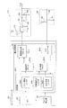
図5(a)は、従来の圧電トランスを用いた高圧電源装置の概略構成図である。尚、後述する実施例で説明する高圧電源装置の構成と同じ構成には同じ符号を付し、詳細は実施例において説明する。圧電トランス101の特性は、一般的に図5(b)のように共振周波数F0において出力電圧が最大となるような裾広がりの形状をしているため、周波数による電圧の制御が可能である。ここで、図5(b)のグラフの横軸は圧電トランス101の駆動周波数(Hz)、縦軸は出力電圧(V)である。尚、周波数と出力電圧の関係は、共振周波数F0で出力が最大となり、共振周波数F0より高い周波数ほど、又は共振周波数F0より低い周波数ほど出力電圧が低下する特徴がある。特許文献1に記載の高圧電源装置では、周波数生成ブロック2015は、最初に共振周波数F0より十分高い周波数Fmaxのパルス信号を出力する。その後、周波数Fmaxから共振周波数F0の間で圧電トランス101の周波数を変化させることによって出力電圧を制御している。即ち、圧電トランス101の出力電圧を増加させるには、周波数を高い方から低い方へ変化させることで可能となる。従って、高圧制御部201は、周波数生成ブロック2015のパルス信号の周波数を増加又は減少させて、出力端子Voutの電圧が目標電圧となるように制御している。
FIG. 5A is a schematic configuration diagram of a high-voltage power supply device using a conventional piezoelectric transformer. In addition, the same code | symbol is attached | subjected to the same structure as the structure of the high voltage power supply device demonstrated in the Example mentioned later, and the detail demonstrates in an Example. The characteristics of the
しかしながら、従来のデジタル制御回路構成では、周波数生成ブロック2015に一般的なデジタルカウンタ回路(例えば、特許文献2参照)を使用するため、以下の課題がある。制御演算ブロック2014は、差分演算ブロック2013の差分演算結果を基に予め決められた演算式で演算を実施し、後段のデジタルカウンタ回路である周波数生成ブロック2015にプリセット値を入力する。デジタルカウンタ回路で構成された周波数生成ブロック2015は、入力されたプリセット値に応じてパルス信号を生成する。即ち、周波数生成ブロック2015は、プリセット値に応じてパルス信号の周波数を増加又は減少させる構成である。このため、周波数と出力電圧の関係が図5(b)のように非線形な特性である圧電トランス101を周波数制御すると、プリセット値と出力電圧の関係は図5(c)のように非線形な特性となる。より詳細に説明すると、圧電トランス101を共振周波数F0付近で制御した場合、周波数に対しての出力電圧は急峻な特性になるため、プリセット値に対しての出力電圧は急峻な特性となる。一方、圧電トランス101を共振周波数F0より十分高い周波数で制御した場合、周波数に対しての出力電圧は緩やかな特性になるため、プリセット値に対しての出力電圧は緩やかな特性となる。そのため、デジタルカウンタ回路で構成された周波数生成ブロック2015で、圧電トランス101を周波数制御すると、図5(c)のようにプリセット値(横軸)と出力電圧(縦軸)の関係は非線形となってしまう。
However, in the conventional digital control circuit configuration, since a general digital counter circuit (see, for example, Patent Document 2) is used for the
また、圧電トランス101を用いた高圧電源装置において、低い電圧を出力しようとすると、差分演算ブロック2013の差分演算結果が小さく、制御演算ブロック2014のプリセット値の増加量も小さくなる。そのため、目標電圧に到達するまでにプリセット値を何度も増加させるために、立ち上り時間が長くなるといった課題が生じてしまう。この課題に対し、例えば特許文献3に記載の高圧電源装置のように、出力端子Voutの電圧に応じて制御のゲインを切り替えることで、立ち上り時間を速くすることが可能である。しかし、エンジンコントローラ501のシステムが複雑になってしまうという課題がある。より詳細に説明すると、高圧制御部201は、出力端子Voutの電圧を記憶部2011の出力電圧レジスタ2022に逐次格納し、出力電圧レジスタ2022の情報をCPU301へ送信するという動作が増える。CPU301は、逐次送信される出力電圧レジスタ2022の情報に基づいて制御のゲインを決定し、記憶部2011にゲインを格納するという動作が増える。そのため、高圧電源装置を制御するシステムが複雑になってしまい、開発コストの増大、エンジンコントローラ501のコストの増大などの課題が生じてしまう。更に、例えば特許文献3に記載の高圧電源装置では、画像形成動作中の瞬間的な負荷変動等によって圧電トランス101の出力が変化し、制御のゲインが切り替わってしまうと、安定した出力電圧を得られない可能性がある。そして、これにより形成される画像の画質が低下してしまう可能性がある。
Further, in a high-voltage power supply device using the
このような画像形成動作の高速化や画質に与える影響は、従来求められていた画像形成装置の性能に対しては十分にその要求を満たすものであった。しかしながら、近年は画像形成装置の高品質化、高速化が特に求められており、また圧電トランスを採用した高圧電源装置で目標電圧が低い場合においても迅速に目標電圧を出力したいという要求がある。従って、これに対応するためには、出力電圧の安定性、尚かつ広範囲の電圧を制御する際に、迅速に目標電圧を出力できることが求められている。 Such an effect on the speeding up of the image forming operation and the image quality sufficiently satisfies the requirement for the performance of the image forming apparatus which has been conventionally required. However, in recent years, there has been a particular demand for higher quality and higher speed of image forming apparatuses, and there is a demand for outputting a target voltage quickly even when the target voltage is low in a high-voltage power supply apparatus employing a piezoelectric transformer. Therefore, in order to cope with this, it is required to output the target voltage quickly when controlling the stability of the output voltage and a wide range of voltages.
本発明は、このような状況のもとでなされたもので、圧電トランスを用いた電源装置において、電源装置の出力が安定して得られるとともに、目標電圧までの立ち上り時間を短縮することを目的とする。 The present invention has been made under such circumstances, and in a power supply device using a piezoelectric transformer, the output of the power supply device can be obtained stably and the rise time to the target voltage can be shortened. And
前述の課題を解決するために、本発明は以下の構成を備える。 In order to solve the above-described problems, the present invention has the following configuration.
(1)圧電トランスと、前記圧電トランスを駆動するための駆動信号を生成する信号生成手段と、前記圧電トランスの出力電圧を検出する検出手段と、前記検出手段で検出された前記出力電圧に応じたフィードバック信号と目標電圧に応じた目標電圧信号に基づき、前記信号生成手段からの前記駆動信号の周波数を制御する周波数制御手段と、前記駆動信号の周波数の変化量を設定するための情報を、前記目標電圧の範囲毎に記憶する記憶手段と、を有し、前記周波数制御手段は、前記目標電圧が第一範囲の電圧の場合に、前記記憶手段に記憶されている前記第一範囲に対応する情報に基づき前記駆動信号の周波数の変化量を第一の値に設定することにより、前記駆動信号の周波数を予め設定されている初期周波数から前記目標電圧に対応する周波数までの期間において、前記駆動信号の周波数を前記第一の値毎に変化させ、前記目標電圧が前記第一範囲とは異なり、前記第一範囲の電圧よりも高い第二範囲の電圧の場合に、前記記憶手段に記憶されている前記第二範囲に対応する情報に基づき前記駆動信号の周波数の変化量を前記第一の値よりも小さい第二の値に設定することにより、前記期間において前記駆動信号の周波数を前記第二の値毎に変化させることを特徴とする電源装置。
(2)画像形成手段と、前記画像形成手段に高電圧を供給する電源と、を有し、前記電源は、圧電トランスと、前記圧電トランスを駆動するための駆動信号を生成する信号生成手段と、前記圧電トランスの出力電圧を検出する検出手段と、前記検出手段で検出された前記出力電圧に応じたフィードバック信号と目標電圧に応じた目標電圧信号に基づき、前記信号生成手段からの前記駆動信号の周波数を制御する周波数制御手段と、前記駆動信号の周波数の変化量を設定するための情報を、前記目標電圧の範囲毎に記憶する記憶手段と、を有し、前記周波数制御手段は、前記目標電圧が第一範囲の電圧の場合に、前記記憶手段に記憶されている前記第一範囲に対応する情報に基づき前記駆動信号の周波数の変化量を第一の値に設定することにより、前記駆動信号の周波数を予め設定されている初期周波数から前記目標電圧に対応する周波数までの期間において、前記駆動信号の周波数を前記第一の値毎に変化させ、前記目標電圧が前記第一範囲とは異なり、前記第一範囲の電圧よりも高い第二範囲の電圧の場合に、前記記憶手段に記憶されている前記第二範囲に対応する情報に基づき前記駆動信号の周波数の変化量を前記第一の値よりも小さい第二の値に設定することにより、前記期間において前記駆動信号の周波数を前記第二の値毎に変化させることを特徴とする画像形成装置。
(3)圧電トランスを有する電源装置の動作を制御するためのICにおいて、前記圧電トランスを駆動するための駆動信号を生成する信号生成手段と、前記圧電トランスの出力電圧に応じたフィードバック信号と目標電圧に応じた目標電圧信号に基づき、前記信号生成手段からの前記駆動信号の周波数を制御する周波数制御手段と、前記駆動信号の周波数の変化量を設定するための情報を、前記目標電圧の範囲毎に記憶する記憶手段と、を有し、前記周波数制御手段は、前記目標電圧が第一範囲の電圧の場合に、前記記憶手段に記憶されている前記第一範囲に対応する情報に基づき前記駆動信号の周波数の変化量を第一の値に設定することにより、前記駆動信号の周波数を予め設定されている初期周波数から前記目標電圧に対応する周波数までの期間において、前記駆動信号の周波数を前記第一の値毎に変化させ、前記目標電圧が前記第一範囲とは異なり、前記第一範囲の電圧よりも高い第二範囲の電圧の場合に、前記記憶手段に記憶されている前記第二範囲に対応する情報に基づき前記駆動信号の周波数の変化量を前記第一の値よりも小さい第二の値に設定することにより、前記期間において前記駆動信号の周波数を前記第二の値毎に変化させることを特徴とするIC。
(1) According to the piezoelectric transformer, signal generation means for generating a drive signal for driving the piezoelectric transformer, detection means for detecting an output voltage of the piezoelectric transformer, and the output voltage detected by the detection means Based on the feedback signal and the target voltage signal corresponding to the target voltage, frequency control means for controlling the frequency of the drive signal from the signal generation means, and information for setting the amount of change in the frequency of the drive signal, Storage means for storing each target voltage range, and the frequency control means corresponds to the first range stored in the storage means when the target voltage is a voltage in the first range. by setting the amount of change in the frequency of the drive signal based on the information to the first value, to respond to the target voltage from an initial frequency that is previously set the frequency of the drive signal In the period until the frequency, the frequency of the drive signal is changed for each of the first value, unlike the target voltage is the first range, when the voltage of the high second range than the voltage of the first range Further, by setting the amount of change in the frequency of the drive signal to a second value smaller than the first value based on information corresponding to the second range stored in the storage means , A power supply device that changes the frequency of the drive signal for each of the second values .
(2) an image forming unit; and a power source that supplies a high voltage to the image forming unit, wherein the power source includes a piezoelectric transformer and a signal generating unit that generates a driving signal for driving the piezoelectric transformer. Detecting means for detecting an output voltage of the piezoelectric transformer, and a driving signal from the signal generating means based on a feedback signal corresponding to the output voltage detected by the detecting means and a target voltage signal corresponding to the target voltage. Frequency control means for controlling the frequency of the drive signal, and storage means for storing information for setting the amount of change in the frequency of the drive signal for each range of the target voltage, the frequency control means, when the target voltage is the voltage of the first range, by setting the amount of change in the frequency of the drive signal based on information corresponding to said first range stored in the storage unit in the first value , In the period from the initial frequency which is preset the frequency of the drive signal up to a frequency corresponding to the target voltage, the frequency of the drive signal is changed for each of the first value, the target voltage is the first Unlike the range, when the voltage of the second range is higher than the voltage of the first range, the amount of change in the frequency of the drive signal is calculated based on the information corresponding to the second range stored in the storage means. An image forming apparatus , wherein the frequency of the drive signal is changed for each of the second values in the period by setting the second value smaller than the first value.
(3) In an IC for controlling the operation of a power supply device having a piezoelectric transformer, signal generating means for generating a drive signal for driving the piezoelectric transformer, a feedback signal corresponding to the output voltage of the piezoelectric transformer, and a target Based on a target voltage signal corresponding to a voltage, frequency control means for controlling the frequency of the drive signal from the signal generation means, and information for setting the amount of change in the frequency of the drive signal, the range of the target voltage Storage means for storing each, and the frequency control means, when the target voltage is a voltage in the first range, based on the information corresponding to the first range stored in the storage means by setting the amount of change in the frequency of the drive signal to the first value, a frequency corresponding to the target voltage from an initial frequency that is previously set the frequency of the drive signal or In the period, the frequency of the drive signal is changed for each of the first value, unlike the target voltage is the first range, when the voltage of the high second range than the voltage of the first range, By setting the amount of change in the frequency of the drive signal to a second value smaller than the first value based on information corresponding to the second range stored in the storage means, the drive in the period An IC , wherein a frequency of a signal is changed for each of the second values .
本発明によれば、圧電トランスを用いた電源装置において、電源装置の出力が安定して得られるとともに、目標電圧までの立ち上り時間を短縮することが可能となる。 According to the present invention, in the power supply device using the piezoelectric transformer, the output of the power supply device can be stably obtained, and the rise time to the target voltage can be shortened.
以下に、本発明の構成及び動作について説明する。尚、以下に示す実施例は一例であって、この発明の技術的範囲をそれらのみに限定する趣旨のものではない。以下、添付図面を参照しながら、本発明を実施するための形態を、実施例により詳しく説明する。 The configuration and operation of the present invention will be described below. In addition, the Example shown below is an example, Comprising: It is not the meaning which limits the technical scope of this invention only to them. Hereinafter, embodiments for carrying out the present invention will be described in detail with reference to the accompanying drawings.
[画像形成装置]
実施例1の画像形成装置について説明する。本実施例では、高圧電源装置を画像形成装置としてのカラーレーザプリンタに適用した場合を例に説明する。図1(a)に、本実施例の画像形成装置としてのカラーレーザプリンタの概略断面図を示す。レーザビームプリンタ10は、不図示のトレイに格納された記録紙11(記録媒体)を繰り出すピックアップローラ12、ピックアップローラ12によって繰り出された記録紙11を搬送するための給紙ローラ13を備える。給紙ローラ13の記録紙11の搬送方向下流には、二次転写部26と中間転写ベルト24を備える。給紙ローラ13により供給された記録紙11は、二次転写部26によって中間転写ベルト24上に転写されたトナー像(現像剤像)が転写されてカラー画像が形成される。トナー像は画像形成部により形成される。
[Image forming apparatus]
An image forming apparatus according to the first exemplary embodiment will be described. In this embodiment, a case where the high voltage power supply device is applied to a color laser printer as an image forming apparatus will be described as an example. FIG. 1A is a schematic sectional view of a color laser printer as an image forming apparatus of the present embodiment. The
ここで、画像形成部は、静電潜像が形成される像担持体としての感光ドラム21a〜21dと、感光ドラム21a〜21dを一様に帯電する帯電部22a〜22dとを備える。また、画像形成部は、感光ドラム21a〜21dに形成された静電潜像をトナーで現像する現像部23a〜23dと、感光ドラム21a〜21d上に現像されたトナー像を中間転写ベルト24に転写する一次転写部25a〜25dとを備える。尚、画像形成部の符号a〜dは、例えばイエロー色、マゼンタ色、シアン色、ブラック色を表しており、以下必要な場合を除き省略する。更に記録紙11の搬送方向下流には、記録紙11に転写されたトナー像を熱定着するために、内部に加熱用のヒータと加圧ローラを有する定着部27を備える。尚、本実施例の電源装置を備える画像形成装置は、上述した構成の画像形成装置に限定されない。
Here, the image forming unit includes
[高圧電源装置と負荷]
図1(b)は、レーザビームプリンタ10に設けられる複数の高圧電源装置と高電圧が印加される負荷である帯電部22、現像部23、一次転写部25、二次転写部26の構成ブロックを示す。尚、図1(b)に示す負荷は図1(a)の構成の画像形成装置に対応したものであり、他の構成の画像形成装置に本実施例の電源装置を適用する場合には、その画像形成装置に対応した負荷に電圧を印加することとなる。
[High-voltage power supply and load]
FIG. 1B is a block diagram of a plurality of high-voltage power supply devices provided in the
エンジンコントローラ501は、CPU301、高圧制御部201a〜201dで構成される。帯電部22、現像部23、一次転写部25、二次転写部26は、画像形成の各処理を行うために、高圧電源装置から所定の高電圧を印加される必要がある。そこで、高圧制御部201aは、帯電部22に印加されている高電圧を電圧検出回路108a(後述する図2参照、以下同じ)で検出し、検出した電圧がCPU301から設定された目標電圧になるように昇圧回路114aを制御する。また、高圧制御部201bは、現像部23に印加されている高電圧を電圧検出回路108bで検出し、検出した電圧がCPU301から設定された目標電圧になるように昇圧回路114bを制御する。また、高圧制御部201cは、一次転写部25に印加されている高電圧を電圧検出回路108cで検出し、検出した電圧がCPU301から設定された目標電圧になるように昇圧回路114cを制御する。また、高圧制御部201dは、二次転写部26に印加されている高電圧を電圧検出回路108dで検出し、検出した電圧がCPU301から設定された目標電圧になるように昇圧回路114dを制御する。
The
[高圧電源装置の構成]
本実施例の高圧電源装置の構成について詳細に説明する。本実施例は、圧電トランス101を用いた高圧電源装置において、目標電圧に応じて制御ゲインを切り替えることを特徴としている。図2は、本実施例の高圧電源装置を示す構成図である。高圧電源装置は、昇圧回路114と、電圧検出回路108(検出手段)と、エンジンコントローラ501とを備える。ここで、昇圧回路114は、図1(b)で説明した昇圧回路114a〜114dに、電圧検出回路108は電圧検出回路108a〜108dに、それぞれ対応している。昇圧回路114は、圧電トランス101、整流用のダイオード102、103、整流用のコンデンサ104、電界効果トランジスタ111、電圧共振用のインダクタ112、電圧共振用のコンデンサ113で構成される。電界効果トランジスタ111は、後述する高圧制御部201から供給されたパルス信号でスイッチング動作し、インダクタ112及びコンデンサ113によるLC共振回路によってパルス信号を増幅する。圧電トランス101は、一次側端子に供給されたパルス信号に応じて振動し、二次側端子に圧電トランス101のサイズに応じた昇圧比で増幅した交流電圧を発生させる。
[Configuration of high-voltage power supply unit]
The configuration of the high-voltage power supply device according to this embodiment will be described in detail. The present embodiment is characterized in that the control gain is switched in accordance with the target voltage in the high-voltage power supply apparatus using the
圧電トランス101の後段には整流回路が接続されている。即ち、圧電トランス101の二次側端子は、ダイオード102のカソード端子と、ダイオード103のアノード端子とに接続されている。コンデンサ104の一端は、ダイオード103のカソード端子に接続され、かつ、出力端子Voutに接続されている。コンデンサ104の他端は、ダイオード102のアノード端子に接続され、かつ、接地されている。ダイオード102、ダイオード103及びコンデンサ104は、整流回路を形成している。従って、圧電トランス101の二次側端子から出力された交流電圧は、この整流回路によって正電圧に整流平滑され、出力端子Voutから負荷(不図示)に供給される。
A rectifier circuit is connected to the subsequent stage of the
電圧検出回路108は、抵抗105、106、107で構成される。出力端子Voutの電圧は、電圧検出回路108で分圧され、分圧後の電圧は、後述する高圧制御部201のA/Dコンバータ2012へ入力される。
The
エンジンコントローラ501は、高圧制御部201、CPU301、クロック発生部401で構成される。高圧制御部201は、図1(b)で説明した高圧制御部201a〜201dに対応しており、出力端子Voutの電圧の定電圧制御を行う。CPU301は、高圧制御部201に目標電圧を設定する。クロック発生部401は、高圧制御部201及びCPU301にそれぞれクロックを供給する。
The
[高圧電源装置の制御動作]
次に、図2に示す高圧電源装置の制御動作について説明する。高圧制御部201は、揮発性メモリである記憶部2011(記憶手段)と、A/Dコンバータ2012と、差分演算ブロック2013と、制御演算ブロック2014と、デジタルカウンタ回路を用いた周波数生成ブロック2015とを備える。また、記憶部2011は、目標値設定レジスタ2021と、出力電圧レジスタ2022と、ゲイン設定レジスタ2023とを備える。図5(a)に示す従来の高圧電源装置と異なる点は、本実施例の高圧電源装置において記憶部2011がゲイン設定レジスタ2023を有する点である。
[Control operation of high-voltage power supply]
Next, the control operation of the high-voltage power supply device shown in FIG. 2 will be described. The high
A/Dコンバータ2012に入力された出力端子Voutの出力は、デジタル変換されたのちに記憶部2011の出力電圧レジスタ2022に格納される。目標電圧は、CPU301から記憶部2011の目標値設定レジスタ2021とゲイン設定レジスタ2023に格納される。差分演算ブロック2013は、出力電圧レジスタ2022と目標値設定レジスタ2021に格納されたそれぞれの値の差分を演算し、制御演算ブロック2014に出力する。
The output of the output terminal Vout input to the A /
制御演算ブロック2014は、差分演算ブロック2013の差分演算結果に基づいてPID制御を行い、周波数生成ブロック2015で生成するパルス信号の周波数を決定するための値であるプリセット値を演算し、周波数生成ブロック2015に入力する。そして、制御演算ブロック2014から入力される周波数制御用のプリセット値が小さくなると、周波数生成ブロック2015はパルス信号の周波数を高くする。一方、制御演算ブロック2014から入力される周波数制御用のプリセット値が大きくなると、周波数生成ブロック2015はパルス信号の周波数を低くする。
The
[周波数生成ブロック]
続いて、周波数生成ブロック2015の構成及び動作について図3(a)を用いて詳細に説明する。周波数生成ブロック2015は、Nbitプログラマブルカウンタ20151と、1bitカウンタ20153と、ANDゲート20154を備える。
[Frequency generation block]
Next, the configuration and operation of the
Nbitプログラマブルカウンタ20151(以下、Nbitカウンタ20151とする)には、クロック発生部401から入力パルス(例えば数MHzのクロック)が供給される。Nbitカウンタ20151は、入力パルスがハイレベル(以下、Hとする)になるたびにカウント値を+1ずつカウントアップしていくことで、カウントを行う。また、Nbitカウンタ20151は、制御演算ブロック2014から入力されるプリセット値と前述のカウント値が一致すると出力が反転し、前述のカウント値はゼロ(0)にクリアされる。Nbitカウンタ20151の出力は、後述する1bitカウンタ20153に出力される。尚、Nbitカウンタ20151は、リセット入力端子RESETにリセット信号としてローレベル(以下、Lとする)の信号が入力されると、リセットがかかり、カウント値はゼロ(0)になる。Nbitカウンタ20151に入力されるリセット信号は、CPU301から供給される。
An input pulse (for example, a clock of several MHz) is supplied from the
1bitカウンタ20153は、Nbitカウンタ20151からの出力信号がH信号となるたびに出力電圧を反転するもので、Nbitカウンタ20151を介して入力されるプリセット値の情報に応じた周波数のパルス信号を生成する。尚、1bitカウンタ20153は、リセット入力端子RESETにリセット信号が入力されるとリセットされる。1bitカウンタ20153に入力されるリセット信号は、CPU301から供給される。
The 1-
これにより、制御演算ブロック2014から入力されるプリセット値が小さくなると、Nbitカウンタ20151から出力される信号が反転する周期が短くなるため、周波数生成ブロック2015から出力されるパルス信号の周波数は高くなる。一方、制御演算ブロック2014から入力されるプリセット値が大きくなると、Nbitカウンタ20151から出力される信号が反転する周期が長くなるため、周波数生成ブロック2015から出力されるパルス信号の周波数は低くなる。
As a result, when the preset value input from the
ANDゲート20154は、CPU301から出力されたENABLE信号に応じて、高圧電源装置の出力のオンオフ(以下、ON/OFFとする)制御を行う。より詳細に説明すると、ENABLE信号がL出力の場合、ANDゲート20154は、1bitカウンタ20153の出力に応じたパルス信号を出力する。一方、ENABLE信号がH出力の場合、ANDゲート20154の出力が強制的にL信号になるため、ANDゲート20154は、L信号を出力する。従って、CPU301から出力されたENABLE信号に応じて、高圧制御部201から出力されるパルス信号のオン/オフ制御を行うことができるため、高圧電源装置の出力のオン/オフ制御を行うことができる。
The AND
尚、上述した図5(b)の周波数Fmaxから共振周波数F0の間で圧電トランス101の周波数を変化させる場合、制御演算ブロック2014のプリセット値にリミット値Fmax、F0を設ければよい。即ち、プリセット値がリミット値Fmax、F0になったら、制御演算ブロック2014のPID制御の演算動作を停止(演算結果を保持)すればよい。その際、リミット値Fmax、F0は、記憶部2011に記憶してもよいし、CPU301から設定可能としてもよいし、固定値にしてもよい。
When the frequency of the
[制御ゲインの切り替え動作]
本実施例の高圧電源装置における、設定電圧値(目標電圧値)に応じて制御ゲインを切り替える動作について説明する。図3(b)は本実施例の設定電圧値に応じて制御ゲインを設定するためのテーブル800を示す図である。テーブル800は、高圧電源装置の設定電圧値(Tgt[V])と、制御演算ブロック2014の制御ゲインパラメータ群(以下、ゲイン又は制御ゲインともいう)との対応関係を定義したルックアップテーブルの一例である。設定電圧値とゲインを対応付けたテーブル800は、CPU301に含まれるROMに予め格納される。尚、テーブル800の制御ゲインパラメータ群は、フィードバック制御の一例としてのPID制御の比例項(P項)、積分項(I項)、微分項(D項)それぞれのゲインのパラメータである。即ち、PID制御を行うための制御パラメータの設定値であり、高圧電源装置の回路が持つ時間遅れ要素、電圧検出回路108や高圧制御部201のA/Dコンバータ2012が持つ時間遅れ要素を考慮し、設定電圧値ごとに最適化した値になっている。また、テーブル800には、高圧電源装置の設定電圧値と制御演算ブロック2014の制御ゲインパラメータ群との対応関係を定義した関係式が定義されてもよい。
[Control gain switching operation]
An operation of switching the control gain according to the set voltage value (target voltage value) in the high-voltage power supply device of the present embodiment will be described. FIG. 3B shows a table 800 for setting the control gain according to the set voltage value of this embodiment. The table 800 is an example of a lookup table that defines a correspondence relationship between the set voltage value (Tgt [V]) of the high-voltage power supply device and a control gain parameter group (hereinafter also referred to as gain or control gain) of the
(設定電圧値が低い場合)
低い電圧を得るために、圧電トランス101を周波数制御した場合、周波数生成ブロック2015は、周波数に対しての出力電圧が緩やかな領域で圧電トランス101を駆動することになる(図5(b)参照)。従って、制御演算ブロック2014のプリセット値に対しての出力電圧は緩やかな特性となる(図5(c)参照)。そこで、本実施例では、CPU301は制御演算ブロック2014のPID制御のゲインを大きくし、制御演算ブロック2014のプリセット値を大きく変化させることで、パルス信号の周波数を大きく変化させることが可能となる。即ち、CPU301は、設定電圧値とその設定電圧値に対応した制御ゲインパラメータ群(図3(b)ではG1に相当するパラメータ群)を、記憶部2011の目標値設定レジスタ2021とゲイン設定レジスタ2023にそれぞれ設定する。
(When the set voltage value is low)
When the frequency of the
ここで、G1とは、例えば目標電圧が1000V未満の低い電圧(Tgt<1000)を得るために最適化したゲイン群であり、本実施例では、比例項(P項)=10、積分項(I項)=8、微分項(D項)=4とする。そして、制御演算ブロック2014のPID制御は、比例項(P項)、積分項(I項)、微分項(D項)それぞれに用いられるゲインを変更することで、制御演算ブロック2014のプリセット値を大きく変化させることが可能である。その結果、周波数に対しての出力電圧が緩やかな領域で圧電トランス101を駆動する場合であっても、プリセット値をより大きく変化させることができるため、迅速に目標電圧を出力することが可能となる。
Here, G1 is a gain group optimized for obtaining a low voltage (Tgt <1000) with a target voltage of less than 1000 V, for example, and in this embodiment, proportional term (P term) = 10, integral term ( I term) = 8 and differential term (D term) = 4. The PID control of the
(設定電圧値が高い場合)
逆に、高い電圧を得るために、圧電トランス101を周波数制御した場合、周波数生成ブロック2015は、周波数に対しての出力電圧が急峻な領域で圧電トランス101を駆動することになる(図5(b)参照)。従って、制御演算ブロック2014のプリセット値に対しての出力電圧は急峻な特性となる(図5(c)参照)。そこで、本実施例では、CPU301は制御演算ブロック2014のPID制御のゲインを変更し、制御演算ブロック2014のプリセット値を細かく変化させることで、パルス信号の周波数を細かく変化させることが可能となる。即ち、CPU301は、設定電圧値とその設定電圧値に対応した制御ゲインパラメータ群(図3(b)ではG5に相当するパラメータ群)を、記憶部2011の目標値設定レジスタ2021とゲイン設定レジスタ2023にそれぞれ設定する。
(When the set voltage value is high)
Conversely, when the frequency of the
ここで、G5とは、例えば目標電圧が4000V以上(4000≦Tgt)の高い電圧を得るために最適化したゲイン群であり、本実施例では、比例項(P項)=6、積分項(I項)=4、微分項(D項)=4とする。そして、制御演算ブロック2014のPID制御は、比例項(P項)、積分項(I項)、微分項(D項)それぞれに用いられるゲインを変更することで、G1より制御演算ブロック2014のプリセット値を細かく変化させることが可能である。その結果、周波数に対しての出力電圧が急峻な領域で圧電トランス101を駆動する場合であっても、従来のPID制御のゲインで演算することができる。このため、従来の立ち上り時間と同等で目標電圧を出力することが可能になると共に、オーバーシュートすることなく、安定した電圧を出力することが可能となる。
Here, G5 is, for example, a gain group optimized for obtaining a high voltage with a target voltage of 4000 V or more (4000 ≦ Tgt). In this embodiment, proportional term (P term) = 6, integral term ( I term) = 4 and differential term (D term) = 4. The PID control of the
以上のように、本実施例の構成によれば、設定電圧値に応じてPID制御のゲインを切り替えることで、圧電トランスを用いた高圧電源装置で低い電圧を出力した際も迅速に目標電圧を出力することが可能となる。 As described above, according to the configuration of this embodiment, the target voltage can be quickly obtained even when a low voltage is output by a high voltage power supply device using a piezoelectric transformer by switching the gain of PID control according to the set voltage value. It becomes possible to output.
[他の実施例]
尚、上述の説明においては、出力端子Voutの電圧は、電圧検出回路108で分圧され、分圧後の電圧を高圧制御部201のA/Dコンバータ2012に入力する場合について説明したが、本実施例は上述の場合に限定されるわけではない。例えば、差分演算ブロック2013を図4(a)の125のようにアナログ回路で構成してもよい。即ち、125は、オペアンプ120と、抵抗121、122、123、124で構成された差動増幅回路であり、以降、差動増幅回路125(出力手段)とする。出力端子Voutの電圧は、電圧検出回路108で分圧され、分圧後の電圧は抵抗121を介してオペアンプ120の反転入力端子(−端子)に入力する。
[Other embodiments]
In the above description, the case where the voltage at the output terminal Vout is divided by the
一方、CPU301により目標値設定レジスタ2021に設定された設定電圧値(目標電圧値)はD/Aコンバータ2016に出力される。そしてD/Aコンバータ2016から出力された設定電圧値は、抵抗123を介してオペアンプ120の非反転入力端子(+端子)に入力する。オペアンプ120は、反転入力端子と非反転入力端子で仮想短絡(バーチャルショート)が成立するように出力する。オペアンプ120の出力は、A/Dコンバータ2012を介して、制御演算ブロック2014へ入力される。従って、差動増幅回路125は、差分演算ブロック2013と同様に、出力端子Voutの電圧と設定電圧値との差分を出力することが可能である。そして、制御演算ブロック2014は、差動増幅回路125により出力された差分をA/Dコンバータ2012によりデジタル変換した値に基づいて、プリセット値を出力する。尚、図4(a)の構成と同じ構成には同じ符号を付し、説明は省略する。
On the other hand, the set voltage value (target voltage value) set in the target
以上、本実施例によれば、圧電トランスを用いた電源装置において、電源装置の出力が安定して得られるとともに、目標電圧までの立ち上り時間を短縮することが可能となる。 As described above, according to this embodiment, in the power supply device using the piezoelectric transformer, the output of the power supply device can be stably obtained, and the rise time to the target voltage can be shortened.
[高圧電源装置]
実施例2の構成及び動作について図4(b)を用いて詳細に説明する。実施例1では、テーブル800は、CPU301に含まれるROMに予め格納され、CPU301が記憶部2011のゲイン設定レジスタ2023に制御ゲインパラメータ群を設定する。本実施例では、実施例1の構成に対して、CPU301に格納していたテーブル800(図3(b)参照)を、高圧制御部201の記憶部2011に格納した点が異なる。本実施例では、実施例1と共通する構成については説明を省略し、テーブル800を高圧制御部201の記憶部2011に格納した構成及び動作について詳細に説明する。
[High-voltage power supply]
The configuration and operation of the second embodiment will be described in detail with reference to FIG. In the first embodiment, the table 800 is stored in advance in a ROM included in the
図4(b)は、本実施例の高圧電源装置を示す構成図である。2017は実施例1のテーブル800を格納したゲイン設定テーブルであり、設定電圧値(目標電圧値)と制御演算ブロック2014のPID制御ゲインパラメータとの対応関係を定義したルックアップテーブルの一例である。尚、テーブル800のPID制御ゲインパラメータ群は、実施例1と同様に設定電圧値ごとに最適化した値になっている。またテーブル800には、実施例1と同様に高圧電源装置の設定電圧値と、制御演算ブロック2014の制御ゲインパラメータ群との対応関係を定義した関係式が定義されてもよい。
FIG. 4B is a configuration diagram illustrating the high-voltage power supply device according to the present embodiment.
制御演算ブロック2014は、ゲイン設定テーブル2017から設定電圧値に対応した制御ゲインパラメータ群でPID制御演算を行うことが可能である。従って、実施例1と同様に、設定電圧値に応じて制御ゲインを切り替えることで、高圧電源装置の出力が安定して得られるとともに、低い電圧を出力した際も迅速に目標電圧を出力することが可能となる。
The
また、本実施例のようにテーブル800を高圧制御部201の記憶部2011に格納することで、CPU301は高圧制御部201の記憶部2011に目標電圧のみ設定すればよい。このため、高圧制御部201のレジスタの数を減らすことができ、尚かつCPU301を介さない制御を行うことが可能である。
Further, by storing the table 800 in the
尚、本実施例においても、実施例1のように差分演算ブロック2013をアナログ回路である差動増幅回路125としてもよい。
Also in this embodiment, the
また、上述した実施例1、2のテーブル800の制御ゲインパラメータ群の値G1、G2、G3、G4、G5は、設定電圧値ごとにG1>G2>G3>G4>G5を満たす最適化した値としたが、本発明はこれに限られない。例えば、高圧電源装置が高電圧を供給する部材のインピーダンス変化もテーブル800の制御ゲインパラメータ群の値G1、G2、G3、G4、G5に考慮してもよい。すなわち、図5(b)の駆動周波数と出力電圧の関係は、部材のインピーダンスによっても変化する。このため、部材のインピーダンスを検知し、駆動周波数と出力電圧の特性変化も考慮して、テーブル800の制御ゲインパラメータ群の値G1、G2、G3、G4、G5を最適化することで、高圧電源装置の出力を安定して得ることができる。 Further, the control gain parameter group values G1, G2, G3, G4, and G5 in the table 800 of the first and second embodiments described above are optimized values that satisfy G1> G2> G3> G4> G5 for each set voltage value. However, the present invention is not limited to this. For example, a change in impedance of a member to which the high-voltage power supply device supplies a high voltage may be considered in the control gain parameter group values G1, G2, G3, G4, and G5 of the table 800. That is, the relationship between the drive frequency and the output voltage in FIG. 5B also changes depending on the impedance of the member. For this reason, the impedance of the member is detected, and the control gain parameter group values G1, G2, G3, G4, and G5 of the table 800 are optimized in consideration of the change in the characteristics of the drive frequency and the output voltage, so The output of the apparatus can be obtained stably.
更に、上述した実施例1、2では、制御演算ブロック2014のフィードバック制御の一例としてPID制御を行う例を説明したが、フィードバック制御のゲインを変更することができれば、他の様態のフィードバック制御を用いても良い。
Further, in the first and second embodiments described above, an example in which PID control is performed as an example of feedback control of the
以上、本実施例によれば、圧電トランスを用いた電源装置において、電源装置の出力が安定して得られるとともに、目標電圧までの立ち上り時間を短縮することが可能となる。 As described above, according to this embodiment, in the power supply device using the piezoelectric transformer, the output of the power supply device can be stably obtained, and the rise time to the target voltage can be shortened.
なお、上記の実施例1、2で説明した高圧制御部201をIC化して構成することも可能である、例えばASIC(Application Specific Integrated Circuit)等の特定用途向けのICとして構成することが可能である。IC化すれば、電源装置の回路規模の縮小化ができ、電源装置の回路基板の小型化につながる。
The high-
101 圧電トランス
108 電圧検出回路
201 高圧制御部
101
Claims (14)
前記圧電トランスを駆動するための駆動信号を生成する信号生成手段と、
前記圧電トランスの出力電圧を検出する検出手段と、
前記検出手段で検出された前記出力電圧に応じたフィードバック信号と目標電圧に応じた目標電圧信号に基づき、前記信号生成手段からの前記駆動信号の周波数を制御する周波数制御手段と、
前記駆動信号の周波数の変化量を設定するための情報を、前記目標電圧の範囲毎に記憶する記憶手段と、
を有し、
前記周波数制御手段は、前記目標電圧が第一範囲の電圧の場合に、前記記憶手段に記憶されている前記第一範囲に対応する情報に基づき前記駆動信号の周波数の変化量を第一の値に設定することにより、前記駆動信号の周波数を予め設定されている初期周波数から前記目標電圧に対応する周波数までの期間において、前記駆動信号の周波数を前記第一の値毎に変化させ、前記目標電圧が前記第一範囲とは異なり、前記第一範囲の電圧よりも高い第二範囲の電圧の場合に、前記記憶手段に記憶されている前記第二範囲に対応する情報に基づき前記駆動信号の周波数の変化量を前記第一の値よりも小さい第二の値に設定することにより、前記期間において前記駆動信号の周波数を前記第二の値毎に変化させることを特徴とする電源装置。 A piezoelectric transformer,
Signal generating means for generating a drive signal for driving the piezoelectric transformer;
Detecting means for detecting an output voltage of the piezoelectric transformer;
Frequency control means for controlling the frequency of the drive signal from the signal generation means based on a feedback signal corresponding to the output voltage detected by the detection means and a target voltage signal corresponding to the target voltage;
Storage means for storing information for setting the amount of change in the frequency of the drive signal for each range of the target voltage;
Have
When the target voltage is a voltage in the first range, the frequency control means sets a change amount of the frequency of the drive signal to a first value based on information corresponding to the first range stored in the storage means. By changing the frequency of the drive signal for each of the first values in a period from a preset initial frequency to a frequency corresponding to the target voltage, the frequency of the drive signal is set to In the case where the voltage is different from the first range and the voltage is in the second range higher than the voltage in the first range, the drive signal based on the information corresponding to the second range stored in the storage means. A power supply apparatus , wherein the frequency of the drive signal is changed for each of the second values in the period by setting a frequency change amount to a second value smaller than the first value.
前記周波数制御手段は、前記記憶手段に記憶された前記テーブルを参照し、予め設定された目標電圧に対応付けられたゲインに切り替えることにより、前記周波数の前記変化量を設定することを特徴とする請求項1または2に記載の電源装置。 The storage means includes a table that associates gains as information for setting the amount of change in the frequency for each range of the target voltage,
The frequency control means sets the change amount of the frequency by referring to the table stored in the storage means and switching to a gain associated with a preset target voltage. The power supply device according to claim 1 or 2.
前記周波数制御手段は、前記出力手段により出力された差分をデジタル変換した値に基づいて、前記フィードバック信号を生成することを特徴とする請求項1乃至3のいずれか1項に記載の電源装置。 Output means for outputting a difference between the output voltage detected by the detection means and a preset target voltage;
4. The power supply device according to claim 1, wherein the frequency control unit generates the feedback signal based on a value obtained by digitally converting the difference output by the output unit. 5.
前記画像形成手段に高電圧を供給する電源と、を有し、
前記電源は、圧電トランスと、前記圧電トランスを駆動するための駆動信号を生成する信号生成手段と、前記圧電トランスの出力電圧を検出する検出手段と、前記検出手段で検出された前記出力電圧に応じたフィードバック信号と目標電圧に応じた目標電圧信号に基づき、前記信号生成手段からの前記駆動信号の周波数を制御する周波数制御手段と、前記駆動信号の周波数の変化量を設定するための情報を、前記目標電圧の範囲毎に記憶する記憶手段と、を有し、
前記周波数制御手段は、前記目標電圧が第一範囲の電圧の場合に、前記記憶手段に記憶されている前記第一範囲に対応する情報に基づき前記駆動信号の周波数の変化量を第一の値に設定することにより、前記駆動信号の周波数を予め設定されている初期周波数から前記目標電圧に対応する周波数までの期間において、前記駆動信号の周波数を前記第一の値毎に変化させ、前記目標電圧が前記第一範囲とは異なり、前記第一範囲の電圧よりも高い第二範囲の電圧の場合に、前記記憶手段に記憶されている前記第二範囲に対応する情報に基づき前記駆動信号の周波数の変化量を前記第一の値よりも小さい第二の値に設定することにより、前記期間において前記駆動信号の周波数を前記第二の値毎に変化させることを特徴とする画像形成装置。 Image forming means;
A power supply for supplying a high voltage to the image forming means,
The power source includes a piezoelectric transformer, signal generation means for generating a drive signal for driving the piezoelectric transformer, detection means for detecting an output voltage of the piezoelectric transformer, and the output voltage detected by the detection means. Frequency control means for controlling the frequency of the drive signal from the signal generation means based on a feedback signal according to the target voltage and a target voltage signal according to the target voltage, and information for setting the amount of change in the frequency of the drive signal. Storing means for each range of the target voltage,
When the target voltage is a voltage in the first range, the frequency control means sets a change amount of the frequency of the drive signal to a first value based on information corresponding to the first range stored in the storage means. By changing the frequency of the drive signal for each of the first values in a period from a preset initial frequency to a frequency corresponding to the target voltage, the frequency of the drive signal is set to In the case where the voltage is different from the first range and the voltage is in the second range higher than the voltage in the first range, the drive signal based on the information corresponding to the second range stored in the storage means. An image forming apparatus , wherein the frequency of the drive signal is changed for each of the second values in the period by setting a frequency change amount to a second value smaller than the first value.
前記圧電トランスを駆動するための駆動信号を生成する信号生成手段と、前記圧電トランスの出力電圧に応じたフィードバック信号と目標電圧に応じた目標電圧信号に基づき、前記信号生成手段からの前記駆動信号の周波数を制御する周波数制御手段と、前記駆動信号の周波数の変化量を設定するための情報を、前記目標電圧の範囲毎に記憶する記憶手段と、を有し、
前記周波数制御手段は、前記目標電圧が第一範囲の電圧の場合に、前記記憶手段に記憶されている前記第一範囲に対応する情報に基づき前記駆動信号の周波数の変化量を第一の値に設定することにより、前記駆動信号の周波数を予め設定されている初期周波数から前記目標電圧に対応する周波数までの期間において、前記駆動信号の周波数を前記第一の値毎に変化させ、前記目標電圧が前記第一範囲とは異なり、前記第一範囲の電圧よりも高い第二範囲の電圧の場合に、前記記憶手段に記憶されている前記第二範囲に対応する情報に基づき前記駆動信号の周波数の変化量を前記第一の値よりも小さい第二の値に設定することにより、前記期間において前記駆動信号の周波数を前記第二の値毎に変化させることを特徴とするIC。 In an IC for controlling the operation of a power supply device having a piezoelectric transformer,
The drive signal from the signal generation means based on a signal generation means for generating a drive signal for driving the piezoelectric transformer, a feedback signal corresponding to the output voltage of the piezoelectric transformer and a target voltage signal corresponding to the target voltage Frequency control means for controlling the frequency of the drive signal, and storage means for storing information for setting the amount of change in the frequency of the drive signal for each range of the target voltage,
When the target voltage is a voltage in the first range, the frequency control means sets a change amount of the frequency of the drive signal to a first value based on information corresponding to the first range stored in the storage means. By changing the frequency of the drive signal for each of the first values in a period from a preset initial frequency to a frequency corresponding to the target voltage, the frequency of the drive signal is set to In the case where the voltage is different from the first range and the voltage is in the second range higher than the voltage in the first range, the drive signal based on the information corresponding to the second range stored in the storage means. An IC , wherein the frequency of the drive signal is changed for each of the second values in the period by setting a frequency change amount to a second value smaller than the first value.
前記周波数制御手段は、前記記憶手段に記憶された前記テーブルを参照し、予め設定された目標電圧に対応付けられたゲインに切り替えることにより、前記周波数の前記変化量を設定することを特徴とする請求項9または10に記載のIC。 The storage means includes a table that associates gains as information for setting the amount of change in the frequency for each range of the target voltage,
The frequency control means sets the change amount of the frequency by referring to the table stored in the storage means and switching to a gain associated with a preset target voltage. The IC according to claim 9 or 10.
前記周波数制御手段は、前記出力手段により出力された差分をデジタル変換した値に基づいて、前記フィードバック信号を生成することを特徴とする請求項9乃至11のいずれか1項に記載のIC。 Comprising output means for outputting a difference between the output voltage and a preset target voltage;
The IC according to any one of claims 9 to 11, wherein the frequency control unit generates the feedback signal based on a value obtained by digitally converting the difference output by the output unit.
Priority Applications (6)
| Application Number | Priority Date | Filing Date | Title |
|---|---|---|---|
| JP2013126546A JP6433114B2 (en) | 2012-08-01 | 2013-06-17 | Power supply device, image forming apparatus, and IC |
| US13/951,746 US20140036546A1 (en) | 2012-08-01 | 2013-07-26 | Power supply apparatus, image forming apparatus, and integrated circuit |
| EP13178638.6A EP2693621B1 (en) | 2012-08-01 | 2013-07-30 | Power supply apparatus, image forming apparatus, and integrated circuit |
| KR1020130090774A KR102010595B1 (en) | 2012-08-01 | 2013-07-31 | Power supply apparatus, image forming apparatus, and integrated circuit |
| KR1020170013824A KR101908217B1 (en) | 2012-08-01 | 2017-01-31 | Power supply apparatus and image forming apparatus |
| US15/466,312 US10228649B2 (en) | 2012-08-01 | 2017-03-22 | Power supply apparatus, image forming apparatus, and integrated circuit |
Applications Claiming Priority (3)
| Application Number | Priority Date | Filing Date | Title |
|---|---|---|---|
| JP2012171146 | 2012-08-01 | ||
| JP2012171146 | 2012-08-01 | ||
| JP2013126546A JP6433114B2 (en) | 2012-08-01 | 2013-06-17 | Power supply device, image forming apparatus, and IC |
Publications (3)
| Publication Number | Publication Date |
|---|---|
| JP2014045645A JP2014045645A (en) | 2014-03-13 |
| JP2014045645A5 JP2014045645A5 (en) | 2016-08-04 |
| JP6433114B2 true JP6433114B2 (en) | 2018-12-05 |
Family
ID=48906130
Family Applications (1)
| Application Number | Title | Priority Date | Filing Date |
|---|---|---|---|
| JP2013126546A Active JP6433114B2 (en) | 2012-08-01 | 2013-06-17 | Power supply device, image forming apparatus, and IC |
Country Status (4)
| Country | Link |
|---|---|
| US (2) | US20140036546A1 (en) |
| EP (1) | EP2693621B1 (en) |
| JP (1) | JP6433114B2 (en) |
| KR (2) | KR102010595B1 (en) |
Families Citing this family (6)
| Publication number | Priority date | Publication date | Assignee | Title |
|---|---|---|---|---|
| KR20160026600A (en) | 2014-09-01 | 2016-03-09 | 주식회사 솔루엠 | Apparatus and method for power supplying |
| JPWO2017018327A1 (en) * | 2015-07-28 | 2018-02-15 | 株式会社村田製作所 | Power supply circuit and AC adapter |
| JP6770590B2 (en) * | 2016-06-14 | 2020-10-14 | コーニンクレッカ フィリップス エヌ ヴェKoninklijke Philips N.V. | Actuator device and drive method incorporating an electroactive polymer actuator |
| US10250252B2 (en) * | 2016-11-03 | 2019-04-02 | Semiconductor Components Industries, Llc | Control circuit and method therefor |
| US10671009B2 (en) | 2017-02-13 | 2020-06-02 | Canon Kabushiki Kaisha | Printed circuit board mounting piezoelectric transformer |
| CN109856961B (en) * | 2019-03-11 | 2022-02-11 | 深圳市安健科技股份有限公司 | Bulb voltage control method and device and computer readable storage medium |
Family Cites Families (17)
| Publication number | Priority date | Publication date | Assignee | Title |
|---|---|---|---|---|
| JP2007189880A (en) | 2006-01-16 | 2007-07-26 | Canon Inc | High-voltage power supply and image forming apparatus equipped with the same |
| JP4848853B2 (en) * | 2006-06-16 | 2011-12-28 | セイコーエプソン株式会社 | Piezoelectric actuator driving method, piezoelectric actuator driving apparatus, electronic device |
| JP5207643B2 (en) | 2007-03-08 | 2013-06-12 | キヤノン株式会社 | Image forming apparatus, voltage power supply apparatus, and control method thereof |
| JP5559456B2 (en) * | 2007-08-01 | 2014-07-23 | 三星電子株式会社 | Piezoelectric transformer type high-voltage power supply device and image forming apparatus |
| US8040018B2 (en) * | 2007-08-01 | 2011-10-18 | Samsung Electronics Co., Ltd. | Piezoelectric transformer type high-voltage power apparatus and image forming apparatus |
| US7973520B2 (en) | 2007-08-01 | 2011-07-05 | Samsung Electronics Co., Ltd. | Piezoelectric transformer type high-voltage power apparatus and image forming apparatus |
| JP2009128416A (en) * | 2007-11-20 | 2009-06-11 | Canon Inc | Image forming apparatus and its control method |
| KR100966873B1 (en) * | 2008-05-26 | 2010-06-29 | (주)아이엠 | Apparatus for Generating High Voltage using Piezo Electric Transformer |
| JP5322536B2 (en) | 2008-08-27 | 2013-10-23 | キヤノン株式会社 | Power supply apparatus, image forming apparatus, and control method for power supply apparatus |
| US8265511B2 (en) | 2008-10-29 | 2012-09-11 | Oki Data Corporation | Power source device and image forming apparatus |
| JP2010124601A (en) | 2008-11-19 | 2010-06-03 | Canon Inc | High voltage power supply device |
| JP4902693B2 (en) | 2009-05-28 | 2012-03-21 | 株式会社沖データ | Piezoelectric transformer driving apparatus and image forming apparatus |
| JP5394164B2 (en) | 2009-08-18 | 2014-01-22 | 株式会社沖データ | Power supply device and image forming apparatus |
| JP4902708B2 (en) | 2009-08-27 | 2012-03-21 | 株式会社沖データ | Power supply device and image forming apparatus |
| JP5864845B2 (en) * | 2009-10-27 | 2016-02-17 | キヤノン株式会社 | High voltage power supply device and image forming apparatus |
| JP5473643B2 (en) * | 2010-02-04 | 2014-04-16 | キヤノン株式会社 | Power supply device and image forming apparatus using the same |
| JP5735758B2 (en) * | 2010-05-25 | 2015-06-17 | キヤノン株式会社 | Voltage transformer type high voltage power supply device, high voltage power supply device, and image forming apparatus |
-
2013
- 2013-06-17 JP JP2013126546A patent/JP6433114B2/en active Active
- 2013-07-26 US US13/951,746 patent/US20140036546A1/en not_active Abandoned
- 2013-07-30 EP EP13178638.6A patent/EP2693621B1/en active Active
- 2013-07-31 KR KR1020130090774A patent/KR102010595B1/en active Protection Beyond IP Right Term
-
2017
- 2017-01-31 KR KR1020170013824A patent/KR101908217B1/en active IP Right Grant
- 2017-03-22 US US15/466,312 patent/US10228649B2/en active Active
Also Published As
| Publication number | Publication date |
|---|---|
| US20140036546A1 (en) | 2014-02-06 |
| US20170194876A1 (en) | 2017-07-06 |
| KR20140017450A (en) | 2014-02-11 |
| KR20170015860A (en) | 2017-02-09 |
| EP2693621A2 (en) | 2014-02-05 |
| EP2693621B1 (en) | 2019-11-06 |
| KR101908217B1 (en) | 2018-10-15 |
| JP2014045645A (en) | 2014-03-13 |
| KR102010595B1 (en) | 2019-08-13 |
| US10228649B2 (en) | 2019-03-12 |
| EP2693621A3 (en) | 2017-07-12 |
Similar Documents
| Publication | Publication Date | Title |
|---|---|---|
| JP6433114B2 (en) | Power supply device, image forming apparatus, and IC | |
| JP5247908B2 (en) | Power supply, control circuit, power supply for image forming device | |
| JP4420458B2 (en) | High voltage power supply, image forming device | |
| US8213823B2 (en) | High-voltage power supply device and image forming apparatus including the same | |
| EP3349070A1 (en) | High-voltage power supply apparatus and image forming apparatus | |
| JP2016177278A (en) | Image forming apparatus and image forming method | |
| JP5473643B2 (en) | Power supply device and image forming apparatus using the same | |
| JP2008224778A (en) | Image forming apparatus, voltage power unit and method therefor | |
| JP2008299292A (en) | Voltage power supply device and image forming apparatus | |
| US8513834B2 (en) | Power supply apparatus and image forming apparatus | |
| JP6218466B2 (en) | High voltage power supply device and image forming apparatus | |
| JP6671879B2 (en) | High voltage power supply and image forming apparatus | |
| JP5590943B2 (en) | Image forming apparatus | |
| JP4613938B2 (en) | Image forming apparatus | |
| JP5188022B2 (en) | Image forming apparatus | |
| JP4981323B2 (en) | Power supply for image forming device | |
| JP2019170156A (en) | Motor drive device and image formation apparatus | |
| JP2006201351A (en) | Image forming apparatus | |
| US9977394B2 (en) | Power source device, image forming apparatus and voltage control method | |
| JP4590250B2 (en) | High voltage power supply | |
| JP6379856B2 (en) | Image forming apparatus, control method, and program | |
| JP2021056360A (en) | Image forming apparatus | |
| JP2002153056A (en) | Power device | |
| JP2008281756A (en) | Image forming device | |
| JP2007140210A (en) | Image forming apparatus and control method for high-voltage power source |
Legal Events
| Date | Code | Title | Description |
|---|---|---|---|
| RD03 | Notification of appointment of power of attorney |
Free format text: JAPANESE INTERMEDIATE CODE: A7423 Effective date: 20160215 |
|
| RD04 | Notification of resignation of power of attorney |
Free format text: JAPANESE INTERMEDIATE CODE: A7424 Effective date: 20160215 |
|
| A521 | Request for written amendment filed |
Free format text: JAPANESE INTERMEDIATE CODE: A523 Effective date: 20160616 |
|
| A621 | Written request for application examination |
Free format text: JAPANESE INTERMEDIATE CODE: A621 Effective date: 20160616 |
|
| A977 | Report on retrieval |
Free format text: JAPANESE INTERMEDIATE CODE: A971007 Effective date: 20170512 |
|
| A131 | Notification of reasons for refusal |
Free format text: JAPANESE INTERMEDIATE CODE: A131 Effective date: 20170704 |
|
| A521 | Request for written amendment filed |
Free format text: JAPANESE INTERMEDIATE CODE: A523 Effective date: 20170901 |
|
| RD04 | Notification of resignation of power of attorney |
Free format text: JAPANESE INTERMEDIATE CODE: A7424 Effective date: 20171201 |
|
| A131 | Notification of reasons for refusal |
Free format text: JAPANESE INTERMEDIATE CODE: A131 Effective date: 20180306 |
|
| A521 | Request for written amendment filed |
Free format text: JAPANESE INTERMEDIATE CODE: A523 Effective date: 20180425 |
|
| TRDD | Decision of grant or rejection written | ||
| A01 | Written decision to grant a patent or to grant a registration (utility model) |
Free format text: JAPANESE INTERMEDIATE CODE: A01 Effective date: 20181009 |
|
| A61 | First payment of annual fees (during grant procedure) |
Free format text: JAPANESE INTERMEDIATE CODE: A61 Effective date: 20181106 |
|
| R151 | Written notification of patent or utility model registration |
Ref document number: 6433114 Country of ref document: JP Free format text: JAPANESE INTERMEDIATE CODE: R151 |