JP6428107B2 - Power storage device, electronic device, electric vehicle and power system - Google Patents
Power storage device, electronic device, electric vehicle and power system Download PDFInfo
- Publication number
- JP6428107B2 JP6428107B2 JP2014199044A JP2014199044A JP6428107B2 JP 6428107 B2 JP6428107 B2 JP 6428107B2 JP 2014199044 A JP2014199044 A JP 2014199044A JP 2014199044 A JP2014199044 A JP 2014199044A JP 6428107 B2 JP6428107 B2 JP 6428107B2
- Authority
- JP
- Japan
- Prior art keywords
- power
- battery
- voltage
- power storage
- module
- Prior art date
- Legal status (The legal status is an assumption and is not a legal conclusion. Google has not performed a legal analysis and makes no representation as to the accuracy of the status listed.)
- Active
Links
Images


Classifications
-
- H—ELECTRICITY
- H02—GENERATION; CONVERSION OR DISTRIBUTION OF ELECTRIC POWER
- H02J—ELECTRIC POWER NETWORKS; CIRCUIT ARRANGEMENTS OR SYSTEMS FOR SUPPLYING OR DISTRIBUTING ELECTRIC POWER; SYSTEMS FOR STORING ELECTRIC ENERGY
- H02J7/00—Circuit arrangements for charging or discharging batteries or for supplying loads from batteries
- H02J7/50—Circuit arrangements for charging or discharging batteries or for supplying loads from batteries acting upon multiple batteries simultaneously or sequentially
- H02J7/52—Circuit arrangements for charging or discharging batteries or for supplying loads from batteries acting upon multiple batteries simultaneously or sequentially for charge balancing, e.g. equalisation of charge between batteries
- H02J7/56—Active balancing, e.g. using capacitor-based, inductor-based or DC-DC converters
-
- B—PERFORMING OPERATIONS; TRANSPORTING
- B60—VEHICLES IN GENERAL
- B60L—PROPULSION OF ELECTRICALLY-PROPELLED VEHICLES; SUPPLYING ELECTRIC POWER FOR AUXILIARY EQUIPMENT OF ELECTRICALLY-PROPELLED VEHICLES; ELECTRODYNAMIC BRAKE SYSTEMS FOR VEHICLES IN GENERAL; MAGNETIC SUSPENSION OR LEVITATION FOR VEHICLES; MONITORING OPERATING VARIABLES OF ELECTRICALLY-PROPELLED VEHICLES; ELECTRIC SAFETY DEVICES FOR ELECTRICALLY-PROPELLED VEHICLES
- B60L50/00—Electric propulsion with power supplied within the vehicle
- B60L50/50—Electric propulsion with power supplied within the vehicle using propulsion power supplied by batteries or fuel cells
- B60L50/60—Electric propulsion with power supplied within the vehicle using propulsion power supplied by batteries or fuel cells using power supplied by batteries
- B60L50/64—Constructional details of batteries specially adapted for electric vehicles
-
- B—PERFORMING OPERATIONS; TRANSPORTING
- B60—VEHICLES IN GENERAL
- B60L—PROPULSION OF ELECTRICALLY-PROPELLED VEHICLES; SUPPLYING ELECTRIC POWER FOR AUXILIARY EQUIPMENT OF ELECTRICALLY-PROPELLED VEHICLES; ELECTRODYNAMIC BRAKE SYSTEMS FOR VEHICLES IN GENERAL; MAGNETIC SUSPENSION OR LEVITATION FOR VEHICLES; MONITORING OPERATING VARIABLES OF ELECTRICALLY-PROPELLED VEHICLES; ELECTRIC SAFETY DEVICES FOR ELECTRICALLY-PROPELLED VEHICLES
- B60L58/00—Methods or circuit arrangements for monitoring or controlling batteries or fuel cells, specially adapted for electric vehicles
- B60L58/10—Methods or circuit arrangements for monitoring or controlling batteries or fuel cells, specially adapted for electric vehicles for monitoring or controlling batteries
- B60L58/18—Methods or circuit arrangements for monitoring or controlling batteries or fuel cells, specially adapted for electric vehicles for monitoring or controlling batteries of two or more battery modules
- B60L58/22—Balancing the charge of battery modules
-
- H—ELECTRICITY
- H01—ELECTRIC ELEMENTS
- H01M—PROCESSES OR MEANS, e.g. BATTERIES, FOR THE DIRECT CONVERSION OF CHEMICAL ENERGY INTO ELECTRICAL ENERGY
- H01M10/00—Secondary cells; Manufacture thereof
- H01M10/05—Accumulators with non-aqueous electrolyte
- H01M10/052—Li-accumulators
- H01M10/0525—Rocking-chair batteries, i.e. batteries with lithium insertion or intercalation in both electrodes; Lithium-ion batteries
-
- H—ELECTRICITY
- H01—ELECTRIC ELEMENTS
- H01M—PROCESSES OR MEANS, e.g. BATTERIES, FOR THE DIRECT CONVERSION OF CHEMICAL ENERGY INTO ELECTRICAL ENERGY
- H01M10/00—Secondary cells; Manufacture thereof
- H01M10/42—Methods or arrangements for servicing or maintenance of secondary cells or secondary half-cells
- H01M10/425—Structural combination with electronic components, e.g. electronic circuits integrated to the outside of the casing
- H01M10/4264—Structural combination with electronic components, e.g. electronic circuits integrated to the outside of the casing with capacitors
-
- H—ELECTRICITY
- H01—ELECTRIC ELEMENTS
- H01M—PROCESSES OR MEANS, e.g. BATTERIES, FOR THE DIRECT CONVERSION OF CHEMICAL ENERGY INTO ELECTRICAL ENERGY
- H01M10/00—Secondary cells; Manufacture thereof
- H01M10/42—Methods or arrangements for servicing or maintenance of secondary cells or secondary half-cells
- H01M10/44—Methods for charging or discharging
- H01M10/441—Methods for charging or discharging for several batteries or cells simultaneously or sequentially
-
- H—ELECTRICITY
- H01—ELECTRIC ELEMENTS
- H01M—PROCESSES OR MEANS, e.g. BATTERIES, FOR THE DIRECT CONVERSION OF CHEMICAL ENERGY INTO ELECTRICAL ENERGY
- H01M4/00—Electrodes
- H01M4/02—Electrodes composed of, or comprising, active material
- H01M4/36—Selection of substances as active materials, active masses, active liquids
- H01M4/58—Selection of substances as active materials, active masses, active liquids of inorganic compounds other than oxides or hydroxides, e.g. sulfides, selenides, tellurides, halogenides or LiCoFy; of polyanionic structures, e.g. phosphates, silicates or borates
- H01M4/5825—Oxygenated metallic salts or polyanionic structures, e.g. borates, phosphates, silicates, olivines
-
- H—ELECTRICITY
- H01—ELECTRIC ELEMENTS
- H01M—PROCESSES OR MEANS, e.g. BATTERIES, FOR THE DIRECT CONVERSION OF CHEMICAL ENERGY INTO ELECTRICAL ENERGY
- H01M4/00—Electrodes
- H01M4/02—Electrodes composed of, or comprising, active material
- H01M4/36—Selection of substances as active materials, active masses, active liquids
- H01M4/58—Selection of substances as active materials, active masses, active liquids of inorganic compounds other than oxides or hydroxides, e.g. sulfides, selenides, tellurides, halogenides or LiCoFy; of polyanionic structures, e.g. phosphates, silicates or borates
- H01M4/583—Carbonaceous material, e.g. graphite-intercalation compounds or CFx
- H01M4/587—Carbonaceous material, e.g. graphite-intercalation compounds or CFx for inserting or intercalating light metals
-
- H—ELECTRICITY
- H01—ELECTRIC ELEMENTS
- H01M—PROCESSES OR MEANS, e.g. BATTERIES, FOR THE DIRECT CONVERSION OF CHEMICAL ENERGY INTO ELECTRICAL ENERGY
- H01M50/00—Constructional details or processes of manufacture of the non-active parts of electrochemical cells other than fuel cells, e.g. hybrid cells
- H01M50/20—Mountings; Secondary casings or frames; Racks, modules or packs; Suspension devices; Shock absorbers; Transport or carrying devices; Holders
- H01M50/204—Racks, modules or packs for multiple batteries or multiple cells
- H01M50/207—Racks, modules or packs for multiple batteries or multiple cells characterised by their shape
- H01M50/213—Racks, modules or packs for multiple batteries or multiple cells characterised by their shape adapted for cells having curved cross-section, e.g. round or elliptic
-
- H—ELECTRICITY
- H01—ELECTRIC ELEMENTS
- H01M—PROCESSES OR MEANS, e.g. BATTERIES, FOR THE DIRECT CONVERSION OF CHEMICAL ENERGY INTO ELECTRICAL ENERGY
- H01M50/00—Constructional details or processes of manufacture of the non-active parts of electrochemical cells other than fuel cells, e.g. hybrid cells
- H01M50/20—Mountings; Secondary casings or frames; Racks, modules or packs; Suspension devices; Shock absorbers; Transport or carrying devices; Holders
- H01M50/249—Mountings; Secondary casings or frames; Racks, modules or packs; Suspension devices; Shock absorbers; Transport or carrying devices; Holders specially adapted for aircraft or vehicles, e.g. cars or trains
-
- H—ELECTRICITY
- H02—GENERATION; CONVERSION OR DISTRIBUTION OF ELECTRIC POWER
- H02J—ELECTRIC POWER NETWORKS; CIRCUIT ARRANGEMENTS OR SYSTEMS FOR SUPPLYING OR DISTRIBUTING ELECTRIC POWER; SYSTEMS FOR STORING ELECTRIC ENERGY
- H02J7/00—Circuit arrangements for charging or discharging batteries or for supplying loads from batteries
- H02J7/50—Circuit arrangements for charging or discharging batteries or for supplying loads from batteries acting upon multiple batteries simultaneously or sequentially
- H02J7/52—Circuit arrangements for charging or discharging batteries or for supplying loads from batteries acting upon multiple batteries simultaneously or sequentially for charge balancing, e.g. equalisation of charge between batteries
-
- H—ELECTRICITY
- H02—GENERATION; CONVERSION OR DISTRIBUTION OF ELECTRIC POWER
- H02J—ELECTRIC POWER NETWORKS; CIRCUIT ARRANGEMENTS OR SYSTEMS FOR SUPPLYING OR DISTRIBUTING ELECTRIC POWER; SYSTEMS FOR STORING ELECTRIC ENERGY
- H02J7/00—Circuit arrangements for charging or discharging batteries or for supplying loads from batteries
- H02J7/90—Regulation of charging or discharging current or voltage
- H02J7/96—Regulation of charging or discharging current or voltage in response to battery voltage
-
- H—ELECTRICITY
- H01—ELECTRIC ELEMENTS
- H01M—PROCESSES OR MEANS, e.g. BATTERIES, FOR THE DIRECT CONVERSION OF CHEMICAL ENERGY INTO ELECTRICAL ENERGY
- H01M10/00—Secondary cells; Manufacture thereof
- H01M10/42—Methods or arrangements for servicing or maintenance of secondary cells or secondary half-cells
- H01M10/425—Structural combination with electronic components, e.g. electronic circuits integrated to the outside of the casing
- H01M2010/4271—Battery management systems including electronic circuits, e.g. control of current or voltage to keep battery in healthy state, cell balancing
-
- H—ELECTRICITY
- H01—ELECTRIC ELEMENTS
- H01M—PROCESSES OR MEANS, e.g. BATTERIES, FOR THE DIRECT CONVERSION OF CHEMICAL ENERGY INTO ELECTRICAL ENERGY
- H01M2220/00—Batteries for particular applications
- H01M2220/20—Batteries in motive systems, e.g. vehicle, ship, plane
-
- Y—GENERAL TAGGING OF NEW TECHNOLOGICAL DEVELOPMENTS; GENERAL TAGGING OF CROSS-SECTIONAL TECHNOLOGIES SPANNING OVER SEVERAL SECTIONS OF THE IPC; TECHNICAL SUBJECTS COVERED BY FORMER USPC CROSS-REFERENCE ART COLLECTIONS [XRACs] AND DIGESTS
- Y02—TECHNOLOGIES OR APPLICATIONS FOR MITIGATION OR ADAPTATION AGAINST CLIMATE CHANGE
- Y02E—REDUCTION OF GREENHOUSE GAS [GHG] EMISSIONS, RELATED TO ENERGY GENERATION, TRANSMISSION OR DISTRIBUTION
- Y02E60/00—Enabling technologies; Technologies with a potential or indirect contribution to GHG emissions mitigation
- Y02E60/10—Energy storage using batteries
-
- Y—GENERAL TAGGING OF NEW TECHNOLOGICAL DEVELOPMENTS; GENERAL TAGGING OF CROSS-SECTIONAL TECHNOLOGIES SPANNING OVER SEVERAL SECTIONS OF THE IPC; TECHNICAL SUBJECTS COVERED BY FORMER USPC CROSS-REFERENCE ART COLLECTIONS [XRACs] AND DIGESTS
- Y02—TECHNOLOGIES OR APPLICATIONS FOR MITIGATION OR ADAPTATION AGAINST CLIMATE CHANGE
- Y02T—CLIMATE CHANGE MITIGATION TECHNOLOGIES RELATED TO TRANSPORTATION
- Y02T10/00—Road transport of goods or passengers
- Y02T10/60—Other road transportation technologies with climate change mitigation effect
- Y02T10/70—Energy storage systems for electromobility, e.g. batteries
Landscapes
- Engineering & Computer Science (AREA)
- Chemical & Material Sciences (AREA)
- General Chemical & Material Sciences (AREA)
- Chemical Kinetics & Catalysis (AREA)
- Electrochemistry (AREA)
- Power Engineering (AREA)
- Manufacturing & Machinery (AREA)
- Mechanical Engineering (AREA)
- Transportation (AREA)
- Sustainable Energy (AREA)
- Sustainable Development (AREA)
- Life Sciences & Earth Sciences (AREA)
- Inorganic Chemistry (AREA)
- Aviation & Aerospace Engineering (AREA)
- Crystallography & Structural Chemistry (AREA)
- Materials Engineering (AREA)
- Microelectronics & Electronic Packaging (AREA)
- Charge And Discharge Circuits For Batteries Or The Like (AREA)
- Secondary Cells (AREA)
- Battery Mounting, Suspending (AREA)
- Battery Electrode And Active Subsutance (AREA)
Description
本開示は、蓄電装置並びに蓄電装置からの電力を利用する電子機器、電動車両および電力システムに関する。 The present disclosure relates to a power storage device, an electronic apparatus that uses power from the power storage device, an electric vehicle, and a power system.
近年では、リチウムイオン電池などの二次電池の用途が太陽電池、風力発電などの新エネルギーシステムと組み合わせた電力貯蔵用蓄電装置、自動車用蓄電池等に急速に拡大している。大出力を発生するために多数の蓄電素子例えば単位電池(単電池、セルとも呼ばれる。以下の説明では、電池セルと適宜称する。)を使用する場合、複数の蓄電モジュールを直列に接続する構成が採用される。蓄電モジュールは、複数個例えば4個の電池セルを並列および/または直列に接続して、電池ブロックを構成する。多数の電池ブロックが外装ケースに収納されて蓄電モジュール(組電池とも呼ばれる。)が構成される。 In recent years, the use of secondary batteries such as lithium-ion batteries has been rapidly expanding to power storage power storage devices combined with new energy systems such as solar batteries and wind power generation, automobile storage batteries, and the like. In the case of using a large number of power storage elements such as unit batteries (also referred to as single cells or cells. In the following description, referred to as battery cells as appropriate) in order to generate a large output, a configuration in which a plurality of power storage modules are connected in series is used. Adopted. The power storage module includes a plurality of, for example, four battery cells connected in parallel and / or in series to form a battery block. A large number of battery blocks are housed in an outer case to constitute a power storage module (also referred to as an assembled battery).
さらに、複数の蓄電モジュールを接続し、複数の蓄電モジュールに対して共通の制御装置を設ける電池システムが知られている。各蓄電モジュールがモジュールコントローラを有し、モジュールコントローラと制御装置との間で通信手段を介して通信する構成とされている。 Furthermore, a battery system in which a plurality of power storage modules are connected and a common control device is provided for the plurality of power storage modules is known. Each power storage module has a module controller, and is configured to communicate between the module controller and the control device via communication means.
複数の電池セルを使用する場合、電池セルの自己放電の相違等に起因して放電時に複数の電池セルの一つが使用下限電圧に到達しても、他の電池セルが未だ使用下限電圧に到達しないことがある。このような状態で、電池セルを再び充電すると、充分に充電することができない電池セルが生じ、電池セルの能力を充分に発揮させることができない問題が生じる。 When using multiple battery cells, even if one of the battery cells reaches the lower limit voltage during discharge due to the difference in self-discharge of the battery cells, the other battery cells still reach the lower limit voltage. There are things that do not. If the battery cell is recharged in such a state, a battery cell that cannot be fully charged is generated, and a problem that the battery cell capability cannot be fully exhibited occurs.
このような複数の電池セル間のバラツキを補正するために、従来から電池セル間のバランスを制御することが行われている。さらに、特許文献1には、多数の電池セルを複数の直列セルグループに分割し、各セルグループにセル間電圧バランス補正回路を設けると共に、グループ間電圧バランス補正回路を設けることが記載されている。グループ間電圧バランス補正回路は、各セルグループの直列電圧をトランス・コイルとスイッチング回路を用いて形成される交流結合によってバランス補正させる構成とされている。
In order to correct such a variation between a plurality of battery cells, conventionally, the balance between the battery cells has been controlled. Furthermore,
特許文献1に記載のグループ間電圧バランス補正回路を蓄電モジュールの電池群のバランスの補正に対して適用することができる。しかしながら、セルグループ毎にコイルが接続されているが、コイルは、共通の磁芯に巻かれている構成である。したがって、別々のケースに収納されている複数の蓄電モジュールに対して接続した場合には、コイルと磁芯とを別のケースに収納する必要がある。この別のトランス装置に対して複数の蓄電モジュールを接続するスター状配線を行うこととなり、蓄電モジュールの個数が増えた場合には、接続が複雑化する問題がある。
The inter-group voltage balance correction circuit described in
さらに、スイッチング回路が同相でオン・オフ動作するように制御されて電圧の均一化がなされるので、セルグループ毎に独立してスイッチング動作を制御することができないものであった。したがって、電圧が高い特定のセルグループから電圧が低い特定のセルグループに対して電力の移送を行うことができない問題があった。さらに、トランスの2次側に共通のコイルおよびスイッチング素子を設けた場合、このスイッチング素子に対して複数のセルグループの直列回路の合計の電圧が印加され、スイッチング素子の耐圧を確保することが難しい問題があった。 Furthermore, since the switching circuit is controlled to be turned on / off in the same phase and the voltage is made uniform, the switching operation cannot be controlled independently for each cell group. Therefore, there is a problem that power cannot be transferred from a specific cell group having a high voltage to a specific cell group having a low voltage. Further, when a common coil and switching element are provided on the secondary side of the transformer, the total voltage of the series circuit of a plurality of cell groups is applied to the switching element, and it is difficult to ensure the withstand voltage of the switching element. There was a problem.
本願出願人は、特許文献2に記載のように、トランスを蓄電モジュールと別の装置として構成する必要がなく、スイッチング素子の耐圧の確保が容易な蓄電装置を提案している。特許文献2に記載の蓄電装置は、各モジュール毎にトランスとスイッチング素子とを設け、スイッチング素子のオン/オフを制御することによって、電圧が高いモジュールから電圧の低いモジュールに電荷を移動させることによって、モジュール間のバランスをとるようにしている。すなわち、高電圧側と低電圧側との電荷量の差を数回に分割して解消すくようにしている。
The applicant of the present application has proposed a power storage device that does not require the transformer to be configured as a separate device from the power storage module as described in
リチウムイオン二次電池として、オリビン型正極材料例えばオリビン型リン酸鉄リチウムを使用したものが知られている。オリビン型リン酸鉄リチウムは、結晶構造か強固で、高温において熱安定性が高い利点有している。オリビン型正極を使用するリチウムイオン二次電池を使用したモジュールの場合、充放電カーブの傾斜が小さく、通常の充放電領域でのセルまたは組電池の電圧差が殆ど現れず、容量のバラツキによる電圧差および容量差は、極めて小さいものである。このようなオリビン型正極を使用するリチウムイオン二次電池を使用するモジュールの場合では、特許文献2に記載されているように、比較的長い周期で数回の電荷移動によって、均等化を行うことができない問題が認められた。
As a lithium ion secondary battery, a battery using an olivine-type positive electrode material such as olivine-type lithium iron phosphate is known. The olivine-type lithium iron phosphate has the advantages of a strong crystal structure and high thermal stability at high temperatures. In the case of a module using a lithium ion secondary battery that uses an olivine-type positive electrode, the slope of the charge / discharge curve is small, the voltage difference between the cells or the assembled battery in the normal charge / discharge region hardly appears, and the voltage due to the variation in capacity The difference and the capacity difference are extremely small. In the case of a module using a lithium ion secondary battery using such an olivine type positive electrode, as described in
したがって、本開示は、オリビン型正極を使用するリチウムイオン二次電池を使用するモジュール間の均等化を行うことができる蓄電装置、電子機器、電動車両および電力システムの提供を目的とする。 Therefore, an object of the present disclosure is to provide a power storage device, an electronic device, an electric vehicle, and an electric power system that can perform equalization between modules using a lithium ion secondary battery using an olivine type positive electrode.
本開示は、それぞれが1の複数の電池セルまたは複数の電池ブロックからなる複数の電池部と、
電池部とそれぞれ並列に接続される第1のコイルおよび第1のスイッチング素子からなる直列回路と、
第1のコイルと電磁的に結合する第2のコイルと、
第2のコイルと直列に接続される第2のスイッチング素子と、
複数の電池部に関連する複数の第2のコイルおよび第2のスイッチング素子の直列回路の両端に対して、第2のスイッチング素子の耐圧を超えない値に設定された電圧を共通に供給するために、共通電源ラインCL+および共通電源ラインCL−の間に挿入されたコンデンサと、
複数の電池部の電圧を等しくするために、第1のスイッチング素子および第2のスイッチング素子に対してコントロールパルス信号を供給する制御部とを備え、
複数の電池部の中で、最も電圧が高い第1の電池部と接続される第1および第2のスイッチング素子によって、第1の電池部から電力が取り出され、
複数の電池部の中で、最も電圧が低い第2の電池部と接続される第1および第2のスイッチング素子によって、第2の電池部に電力が供給され、
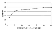
第1の電池部と第2の電池部との間の電圧差をなくすために必要な移動電荷量を1/10以上に分割した電荷量を第1および第2のスイッチング素子のスイッチング動作によって転送するようになされ、
移動電荷量に応じて第1および第2のスイッチング素子のそれぞれのオン期間およびオフ期間が予め求められてテーブルとして構成されている蓄電装置である。
The present disclosure includes a plurality of battery units each including a plurality of battery cells or a plurality of battery blocks,
A series circuit composed of a first coil and a first switching element connected in parallel with the battery unit;
A second coil electromagnetically coupled to the first coil;
A second switching element connected in series with the second coil;
To commonly supply a voltage set to a value not exceeding the breakdown voltage of the second switching element to both ends of the series circuit of the plurality of second coils and the second switching element related to the plurality of battery units. And a capacitor inserted between the common power line CL + and the common power line CL−,
A control unit for supplying a control pulse signal to the first switching element and the second switching element in order to equalize the voltages of the plurality of battery units;
Power is extracted from the first battery unit by the first and second switching elements connected to the first battery unit having the highest voltage among the plurality of battery units,
Power is supplied to the second battery unit by the first and second switching elements connected to the second battery unit having the lowest voltage among the plurality of battery units,
A charge amount obtained by dividing a moving charge amount required to eliminate a voltage difference between the first battery unit and the second battery unit by 1/10 or more is transferred by a switching operation of the first and second switching elements. Was made to
The power storage device is configured as a table in which the ON period and the OFF period of each of the first and second switching elements are obtained in advance according to the amount of mobile charge .
本開示は、上述した蓄電装置を有し、蓄電装置に接続される電子機器に電力を供給する蓄電装置である。
本開示は、上述した蓄電装置から、電力の供給を受ける電子機器である。
本開示は、上述した蓄電装置から、電力の供給を受けて車両の駆動力に変換する変換装置と、蓄電装置に関する情報に基いて車両制御に関する情報処理を行なう制御装置とを有する電動車両である。
本開示は、他の機器とネットワークを介して信号を送受信する電力情報送受信部とを備え、
送受信部が受信した情報に基づき、上述した蓄電装置の充放電制御を行う電力システムである。
本開示は、上述した蓄電装置から、電力の供給を受け、または発電装置または電力網から蓄電装置に電力を供給する電力システムである。
The present disclosure is a power storage device that includes the power storage device described above and supplies power to an electronic device connected to the power storage device.
The present disclosure is an electronic device that receives power supply from the power storage device described above.
The present disclosure is an electric vehicle including a conversion device that receives electric power from the power storage device described above and converts the power into a driving force of the vehicle, and a control device that performs information processing related to vehicle control based on information related to the power storage device. .
The present disclosure includes a power information transmission / reception unit that transmits / receives a signal to / from another device via a network,
The power system performs charge / discharge control of the above-described power storage device based on information received by the transmission / reception unit.
The present disclosure is a power system that receives power supply from the power storage device described above or supplies power to the power storage device from a power generation device or a power network.
本開示のモジュール間バランス回路は、モジュール間の電圧差をなくすために必要な移動電荷量を1/10以上に分割した電荷量を転送するので、電圧差が小さい場合でもバランスをとることができる。 The inter-module balance circuit according to the present disclosure transfers a charge amount obtained by dividing a moving charge amount necessary for eliminating a voltage difference between modules into 1/10 or more, so that even when the voltage difference is small, a balance can be achieved. .
以下に説明する実施の形態は、この発明の好適な具体例であり、技術的に好ましい種々の限定が付されているが、この発明の範囲は、以下の説明において、特にこの発明を限定する旨の記載がない限り、これらの実施の形態に限定されないものとする。 The embodiments described below are preferred specific examples of the present invention, and various technically preferable limitations are given. However, the scope of the present invention is particularly limited in the following description. Unless stated to the effect, the present invention is not limited to these embodiments.
「蓄電システム」
大出力を発生するために多数の蓄電素子例えば電池セルを使用する場合、複数の蓄電ユニット(以下、蓄電モジュールと称する)を接続し、複数の蓄電モジュールに対して共通に制御装置を設ける構成が採用される。かかる構成を蓄電システムと称する。
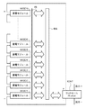
"Power storage system"
When a large number of power storage elements such as battery cells are used to generate a large output, a configuration in which a plurality of power storage units (hereinafter referred to as power storage modules) are connected and a control device is provided in common for the plurality of power storage modules Adopted. Such a configuration is referred to as a power storage system.
蓄電モジュールは、複数の電池セルとコントローラとを組み合わせた単位である。図1に示すように、N個の蓄電モジュールMOD1〜MODNが直列に接続される。蓄電モジュールMOD1〜MODNが絶縁部ISを介してインターフェースバスBSと接続されている。 The power storage module is a unit in which a plurality of battery cells and a controller are combined. As shown in FIG. 1, N power storage modules MOD1 to MODN are connected in series. The power storage modules MOD1 to MODN are connected to the interface bus BS via the insulating part IS.
さらに、各モジュールコントローラが全体の制御装置(以下、コントロールボックスと適宜称する。)ICNTと接続され、コントロールボックスICNTが充電管理、放電管理、劣化抑制等のための管理を行う。コントロールボックスICNTは、マイクロコンピュータによって構成されている。 Further, each module controller is connected to the entire control device (hereinafter referred to as a control box as appropriate) ICNT, and the control box ICNT performs management for charge management, discharge management, deterioration suppression, and the like. The control box ICNT is constituted by a microcomputer.
蓄電モジュール内のバス並びに蓄電モジュールMOD1〜MODNとコントロールボックスICNTとを接続するバスBSとしては、シリアルインターフェースが使用される。シリアルインターフェースとしては、具体的にSMバス(System Management Bus)、CA
N(Controller Area Network)、SPI(Serial Peripheral Interface)等が使用される。例えばI2Cバスを使用することができる。I2Cバスは、SCL(シリアルクロック)と双方向のSDA(シリアル・データ)の2本の信号線で通信を行う同期式のシリアル通信である。
A serial interface is used as the bus in the power storage module and the bus BS connecting the power storage modules MOD1 to MODN and the control box ICNT. Specific serial interfaces include SM bus (System Management Bus), CA
N (Controller Area Network), SPI (Serial Peripheral Interface), etc. are used. For example, an I2C bus can be used. The I2C bus is synchronous serial communication in which communication is performed using two signal lines of SCL (serial clock) and bidirectional SDA (serial data).
各蓄電モジュールMODのモジュールコントローラCNTとコントロールボックスICNTとが通信を行う。すなわち、各蓄電モジュールの内部状態の情報、すなわち、電池情報をコントロールボックスICNTが受け取り、各蓄電モジュールの充電処理および放電処理が管理される。コントロールボックスICNTがN個の蓄電モジュールの直列接続の出力(N×51.2V)を負荷に対して供給する。N=14の例では、出力が(14×51.2V=716.8V)となる。 The module controller CNT and the control box ICNT of each power storage module MOD communicate with each other. That is, the control box ICNT receives information on the internal state of each power storage module, that is, battery information, and the charging process and the discharging process of each power storage module are managed. The control box ICNT supplies an output (N × 51.2 V) of N power storage modules connected in series to the load. In the example of N = 14, the output is (14 × 51.2V = 716.8V).
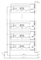
「蓄電モジュールの一例」
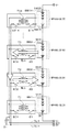
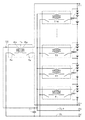
図2は、蓄電モジュールMODの機械的構成を示す斜視図である。蓄電モジュールMODの外装ケースは、板金加工された金属製の外装下ケース2aおよび外装上ケース2bからなる。外装下ケース2aおよび外装上ケース2bの材料としては、高い熱伝導率および輻射率を有する材料を用いることが好ましい。優れた筐体放熱性を得ることができ、ケース内の温度上昇を抑制することができる。例えば、外装下ケース2aおよび外装上ケース2bの材料は、アルミニウムまたはアルミニウム合金または銅または銅合金である。ケースの背面には、蓄電モジュールMODに対して充放電のための外部正極端子3および外部負極端子4が設けられている。
"Example of storage module"
FIG. 2 is a perspective view showing a mechanical configuration of the power storage module MOD. The outer case of the power storage module MOD includes a metal outer lower case 2a and an outer
さらに、蓄電モジュールMODの背面に電流遮断器5が設けられている。電流遮断器5を設けることで、安全性を向上することができる。さらに、ケース2内に配されている制御回路との間の通信用のコネクタ部6が設けられている。制御回路は、電池ユニットの温度の監視を行い、充電、放電等を制御するために設けられている。さらに、ケースの前面には、動作状態を示すLED等の表示素子が設けられている。
Further, a
ケースの外装下ケース2aが箱状の構成を有し、その開口を覆うように、外装上ケース2bが設けられる。外装下ケース2aの収納スペース内に、サブモジュールAS1〜AS4が収納される。サブモジュールAS1〜AS4をビス止め等により固定するために、外装下ケース2aの底面に複数のボスが形成されている。サブモジュールAS1〜AS4は、予めケースの外において組み立てられる。
The exterior lower case 2a of the case has a box-like configuration, and the exterior
各サブモジュールは、複数の電池ブロックを副収納ケースとしての絶縁性のケースによって一体化したものである。サブモジュールのケースとしては、プラスチック等のモールド部品を使用することができる。サブモジュールAS1〜AS4は、内部の電池ブロックの正極端子および負極端子が露出しないように、複数の電池ブロックをケース内に収納するものである。 Each submodule is formed by integrating a plurality of battery blocks by an insulating case as a sub storage case. As the case of the submodule, a molded part such as plastic can be used. The submodules AS1 to AS4 store a plurality of battery blocks in a case so that the positive terminal and the negative terminal of the internal battery block are not exposed.
一つの電池ブロックは、例えば8本の円筒状リチウムイオン2次電池を並列接続したものである。サブモジュールAS1およびAS2は、それぞれ6個の電池ブロックを上ケースおよび下ケースによって一体化したものである。サブモジュールAS3およびAS4は、それぞれ2個の電池ブロックを上ケースおよび下ケースによって一体化したものである。したがって、合計(6+6+2+2=16個)の電池ブロックが使用される。これらの電池ブロックが例えば直列に接続される。 One battery block is formed by connecting, for example, eight cylindrical lithium ion secondary batteries in parallel. The submodules AS1 and AS2 are obtained by integrating six battery blocks by an upper case and a lower case, respectively. The submodules AS3 and AS4 are obtained by integrating two battery blocks by an upper case and a lower case, respectively. Therefore, a total (6 + 6 + 2 + 2 = 16) battery blocks are used. These battery blocks are connected in series, for example.
サブモジュールAS1〜AS4のそれぞれにおいて、電池ブロックを直列接続するために、接続用の金属板例えばバスバーが使用される。バスバーは、細長い棒状の金属である。バスバーには、電池ブロックから導出されている接続金属板等との接続のために複数の穴が形成されている。 In each of the submodules AS1 to AS4, a connection metal plate such as a bus bar is used to connect the battery blocks in series. The bus bar is an elongated rod-shaped metal. A plurality of holes are formed in the bus bar for connection to a connection metal plate or the like led out from the battery block.
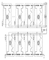
図3に示すように、それぞれ8本の電池が並列に接続された電池ブロックB1〜B16が直列に接続されている。8本の電池を並列接続することは8Pと称される。16個の電池ブロックを直列に接続することは16Sと称される。したがって、図3に示す各モジュールの電池部(電池ブロックグループと適宜称する)BBは、8P16Sの構成を有する
ものとされている。電池ブロックB1〜B16は、それぞれ各蓄電モジュールの制御装置としてのモジュールコントローラCNTに接続され、充放電が制御される。充放電は、外部正極端子3および外部負極端子4を介してなされる。例えば電池ブロックB1〜B6がサブモジュールAS1に含まれており、電池ブロックB11〜B16がサブモジュールAS2に含まれている。さらに、電池ブロックB7およびB10がサブモジュールAS3に含まれ、電池ブロックB8およびB9がサブモジュールAS4に含まれる。
As shown in FIG. 3, battery blocks B1 to B16 each having eight batteries connected in parallel are connected in series. Connecting 8 batteries in parallel is called 8P. Connecting 16 battery blocks in series is referred to as 16S. Therefore, the battery unit (referred to as a battery block group) BB of each module shown in FIG. 3 has a configuration of 8P16S. Battery blocks B1 to B16 are each connected to a module controller CNT as a control device of each power storage module, and charge / discharge is controlled. Charging / discharging is performed via the external
各電池ブロックの正負電極間の電圧等の情報がバス10を介してモジュールコントローラCNTに対して供給される。モジュールコントローラCNTは、各電池ブロックの電圧、電流、および温度をモニタし、モニタした結果を電池情報として出力する。例えば一つの蓄電モジュールMODは、(16×3.2V=51.2V)を出力する。
Information such as the voltage between the positive and negative electrodes of each battery block is supplied to the module controller CNT via the
図4に、蓄電システムのより具体的な接続構成を示す。例えば4個の蓄電モジュールMOD1〜MOD4が直列に接続される。この場合では、正極端子3(VB+)および負極端子4(VB−)に取り出される合計の電圧が約200Vである。各蓄電モジュールには、モジュールコントローラCNT1〜CNT4と電池ブロックグループBB1〜BB4とがそれぞれ含まれている。各電池ブロックグループは、例えば16個の電池ブロックの直列接続である。 FIG. 4 shows a more specific connection configuration of the power storage system. For example, four power storage modules MOD1 to MOD4 are connected in series. In this case, the total voltage extracted to the positive terminal 3 (VB +) and the negative terminal 4 (VB−) is about 200V. Each power storage module includes module controllers CNT1 to CNT4 and battery block groups BB1 to BB4, respectively. Each battery block group is, for example, a series connection of 16 battery blocks.
モジュールコントローラCNT1〜CNT4がバスを介して接続され、モジュールコントローラCNT4の通信端子がコントロールボックスICNTに対して接続されている。コントロールボックスICNTに対して、各モジュールコントローラからのモジュール毎の電圧等の情報が伝送される。コントロールボックスICNTは、さらに、外部との通信が可能なように通信端子11を有する。
Module controllers CNT1 to CNT4 are connected via a bus, and a communication terminal of the module controller CNT4 is connected to the control box ICNT. Information such as voltage for each module from each module controller is transmitted to the control box ICNT. The control box ICNT further includes a
「2次電池の一例について」
本開示の実施の形態において、使用される2次電池の一例は、正極活物質と、黒鉛等の炭素材料を負極活物質として含むリチウムイオン2次電池であり、正極材料としてオリビン構造を有する正極活物質を含有するものである。
“An example of a secondary battery”
In the embodiment of the present disclosure, an example of a secondary battery used is a lithium ion secondary battery including a positive electrode active material and a carbon material such as graphite as a negative electrode active material, and a positive electrode having an olivine structure as a positive electrode material. It contains an active material.
オリビン構造を有する正極活物質としてさらに好ましくは、リチウム鉄リン酸化合物(LiFePO4 )、または、異種原子を含有するリチウム鉄複合リン酸化合物(LiFexM1-xO4 :Mは1種類以上の金属、xは0<x<1である。)が好ましい。ここで、「主体」とは、正極活物質層の正極活物質総質量の50%以上を意味する。また、Mが2種以上の場合は、各々の下付数字の総和が1−xとなるように選定される。 More preferably, as the positive electrode active material having an olivine structure, a lithium iron phosphate compound (LiFePO 4 ) or a lithium iron composite phosphate compound containing different atoms (LiFe x M 1-x O 4 : M is one or more types) And x is preferably 0 <x <1). Here, the “main body” means 50% or more of the total mass of the positive electrode active material in the positive electrode active material layer. Further, when M is two or more kinds, M is selected so that the sum of the subscripts is 1-x.
Mとしては、遷移元素、IIA族元素、IIIA族元素、IIIB族元素、IVB族元素等が挙げられる。特にコバルト(Co),ニッケル,マンガン(Mn),鉄,アルミニウム,バナジウム(V),およびチタン(Ti)のうちの少なくとも1種を含むものが好ましい。 Examples of M include transition elements, IIA group elements, IIIA group elements, IIIB group elements, IVB group elements, and the like. In particular, those containing at least one of cobalt (Co), nickel, manganese (Mn), iron, aluminum, vanadium (V), and titanium (Ti) are preferable.
正極活物質は、リチウム鉄リン酸化合物またはリチウム鉄複合リン酸化合物の表面に、該酸化物とは異なる組成の金属酸化物(例えば、Ni、Mn、Liなどから選択されるもの)やリン酸化合物(例えば、リン酸リチウム等)等を含む被覆層が施されていてもよい。 The positive electrode active material is a metal oxide (for example, selected from Ni, Mn, Li, etc.) or phosphoric acid having a composition different from that of the oxide on the surface of the lithium iron phosphate compound or lithium iron composite phosphate compound. The coating layer containing a compound (for example, lithium phosphate etc.) etc. may be given.
リチウム(Li)を吸蔵および放出することが可能な正極材料として、層状岩塩構造を有するコバルト酸リチウム(LiCoO2)、ニッケル酸リチウム(LiNiO2)、マンガン酸リチウム(LiMnO2)、スピネル構造を有するマンガン酸リチウム(LiMn2O4)などのリチウム複合酸化物が使用されてもよい。 As a positive electrode material capable of inserting and extracting lithium (Li), lithium cobaltate (LiCoO 2 ), lithium nickelate (LiNiO 2 ), lithium manganate (LiMnO 2 ) having a layered rock salt structure, spinel structure A lithium composite oxide such as lithium manganate (LiMn 2 O 4 ) may be used.
負極活物質として使用される黒鉛としては、特に限定はなく、業界において用いられる黒鉛材料を広く用いることができる。負極の材料として、チタン酸リチウム、シリコン(Si)系材料、スズ(Sn)系材料等が使用されてもよい。 There is no limitation in particular as graphite used as a negative electrode active material, The graphite material used in an industry can be used widely. As the negative electrode material, lithium titanate, silicon (Si) -based material, tin (Sn) -based material, or the like may be used.
電池の電極の製造法としては、特に限定はなく、業界において用いられている方法を広く用いることができる。 The method for producing the battery electrode is not particularly limited, and a wide variety of methods used in the industry can be used.
本開示に用いられる電解液としては、特に限定はなく、液状、ゲル状を含み、業界において用いられる電解液を広く用いることができる。 There is no limitation in particular as electrolyte solution used for this indication, The electrolyte solution used in industry including liquid form and a gel form can be used widely.
正極材料としてオリビン構造を有する正極活物質を含有する2次電池を使用したモジュールの放電特性は、正極材料として、NCM(ニッケルコバルトマンガン)を使用する2次電池を使用したモジュールの放電特性と相違している。正極材料としてオリビン構造を有する正極活物質を含有する2次電池のモジュールの場合、放電が進んでも電圧の低下が少ない。SOCが20%〜80%の範囲で電圧差が0.2V/セル以内である。一方、NCMを使用する2次電池を使用したモジュールの場合、放電の進行に伴い、電圧の低下の割合が大きい。 Discharge characteristics of a module using a secondary battery containing a positive electrode active material having an olivine structure as a positive electrode material is different from that of a module using a secondary battery using NCM (nickel cobalt manganese) as the positive electrode material. doing. In the case of a secondary battery module that contains a positive electrode active material having an olivine structure as the positive electrode material, there is little decrease in voltage even when the discharge proceeds. The voltage difference is within 0.2 V / cell when the SOC is in the range of 20% to 80%. On the other hand, in the case of a module using a secondary battery using NCM, the rate of voltage drop is large as the discharge progresses.
「モジュールコントローラの一例」
図5を参照してモジュールコントローラの構成の一例について説明する。モジュールコントローラCNTは、直列に接続されたn個の電池ブロックB1〜Bnの両端の電圧と、各電池ブロックの電圧を検出するようになされる。電池ブロックB1〜Bnの両端の電圧と各電池ブロックの電圧を順次出力するマルチプレクサ15が設けられている。
"Example of module controller"
An example of the configuration of the module controller will be described with reference to FIG. The module controller CNT detects the voltage at both ends of the n battery blocks B1 to Bn connected in series and the voltage of each battery block. A
マルチプレクサ15は、例えば、所定の制御信号に応じてチャネルを切り替え、n個のアナログ電圧データの中から一のアナログ電圧データを選択する。マルチプレクサ15によって選択された一のアナログ電圧データがA/Dコンバータ(図ではADC(Analog to Digital Converter) と表記する)16に供給される。
For example, the
A/Dコンバータ16は、マルチプレクサ15から供給されるアナログ電圧データをデジタル電圧データに変換する。例えばアナログ電圧データが14〜18ビットのデジタル電圧データに変換される。なお、A/Dコンバータ16の方式としては、逐次比較方式やΔΣ(デルタシグマ)方式など、種々の方式を使用できる。
The A /
A/Dコンバータ16からのデジタル電圧データが通信部17に供給される。通信部17は、制御部18によって制御され、通信用端子19aおよび19bを通じて接続される外部の装置との通信を行う。例えば通信用端子19aを通じて他のモジュールのモジュールコントローラとの通信を行い、通信用端子19bを通じてコントロールボックスICNTとの通信を行う。さらに、通信用端子19bを通じてコントロールボックスICNTからの制御信号をモジュールコントローラCNTが受け取る。このように、通信部17が双方向通信を行う。
Digital voltage data from the A /
さらに、制御部18が電池ブロックの電圧の均一化を制御するようになされる。このような制御は、セルバランス制御と称される。例えば複数の電池ブロックB1〜Bnの内で一つの電池ブロックが使用下限の放電電圧まで到達した場合、未だ容量が残っている他の電池ブロックが存在する。次に充電した場合に、容量が残っていた他の電池ブロックが速く充電上限電圧に到達してしまい、満充電まで充電できない。かかるアンバランスを避けるために、容量が残っている電池ブロックをMOSFET(Metal Oxide Semiconductor Field Effect Transistor)をオンさせることによって、強制的に放電するようになされる
。なお、セルバランス制御の方式は、上述したパッシブ方式に限らず、いわゆるアクティブ方式や他の様々な方式を適用できる。本開示におけるモジュール間バランス制御に関しては、後で詳細に説明する。
Further, the
なお、上述したモジュールコントローラCNTは、各電池ブロックの電圧をモニタし、検出した電圧をデジタル信号に変換してコントロールボックスICNTに伝送するものである。電圧に加えて各電池ブロックの温度を検出し、温度をデジタルデータに変換し、コントロールボックスICNTに対して伝送するようにしても良い。 The module controller CNT described above monitors the voltage of each battery block, converts the detected voltage into a digital signal, and transmits the digital signal to the control box ICNT. In addition to the voltage, the temperature of each battery block may be detected, converted into digital data, and transmitted to the control box ICNT.
モジュールコントローラCNTに対する電源は、図5に示すように、電池ブロックB1〜Bnから供給されている。しかしながら、電池ブロックB1〜Bnを電源として使用すると、モジュールコントローラCNTの消費電力が互いに等しくないために、モジュール間の電池ブロックB1〜Bnの間の容量のバラツキが生じ、モジュール間アンバランスが発生する。この点からモジュールコントローラCNTの電源は、電池ブロックB1〜Bnを使用しないことが好ましい。 As shown in FIG. 5, power to the module controller CNT is supplied from battery blocks B1 to Bn. However, when the battery blocks B1 to Bn are used as a power source, the power consumption of the module controller CNT is not equal to each other. Therefore, there is a variation in capacity between the battery blocks B1 to Bn between modules, and an imbalance between modules occurs. . From this point, it is preferable that the power source of the module controller CNT does not use the battery blocks B1 to Bn.
図5に示すモジュールコントローラCNTにおいて、内側の破線で囲んで示すように、A/Dコンバータ16、通信部17および制御部18が低電圧例えば5Vの電源で動作することができる低電圧電源部である。本開示では、低電圧電源部に対する電源をコントロールボックスICNTから供給するようになされる。電池ブロックB1〜Bnから電源を供給すると、モジュールコントローラCNTの消費電力の相違によって、モジュール間のバランスが崩れるおそれがある。本開示では、モジュールコントローラCNTの低電圧電源部に対する電源をコントロールボックスICNTから供給するので、かかる問題を生じない。
In the module controller CNT shown in FIG. 5, the A /
「本開示による蓄電システム」
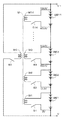
n個の蓄電モジュールMOD1〜MODnを有する蓄電システムに対して本開示を適用した構成を図6に示す。各蓄電モジュールが通信部COM1〜COMnと、絶縁部ISC1〜ISCnと、モジュールコントローラCNT1〜CNTnと、電池ブロックグループBB1〜BBnとから構成されている。n個の蓄電モジュールと、コントロールボックスICNTとが接続される。接続のために、通信用ラインL1およびL2と、電源用ラインLpとが使用される。通信用ラインL1およびL2を通じてコントロールボックスICNTと蓄電モジュールMOD1〜MODnとの間で双方向通信がなされる。通信方式として、例えばCANが使用される。最近では、CANは、車載LANとして使用されている。
"Power storage system according to the present disclosure"
FIG. 6 shows a configuration in which the present disclosure is applied to a power storage system having n power storage modules MOD1 to MODn. Each power storage module includes communication units COM1 to COMn, insulating units ISC1 to ISCn, module controllers CNT1 to CNTn, and battery block groups BB1 to BBn. The n power storage modules and the control box ICNT are connected. For connection, communication lines L1 and L2 and a power supply line Lp are used. Bidirectional communication is performed between the control box ICNT and the power storage modules MOD1 to MODn through the communication lines L1 and L2. For example, CAN is used as the communication method. Recently, CAN is used as an in-vehicle LAN.
各蓄電モジュールの通信部COM1〜COMnは、図5における通信部17に対応する。したがって、図6におけるモジュールコントローラCNT1〜CNTnは、図5の構成に対して通信部17を有しない構成である。但し、通信部COM1〜COMnと通信部17の両者を設けてそれぞれが異なる機能を持つようにしても良い。電源用ラインLpを通じて例えば+5Vの電源電圧が各蓄電モジュールの低電圧電源部の電源として供給される。
The communication units COM1 to COMn of each power storage module correspond to the
絶縁部ISC1〜ISCnは、通信部COM1〜COMnとモジュールコントローラCNT1〜CNTnとの間を絶縁する機能を有する。すなわち、通信部COM1〜COMnの電源の基準電位と、モジュールコントローラCNT1〜CNTnの電源の基準電位とが分離され、独立したものとされる。さらに、絶縁した状態において、絶縁部ISC1〜ISCnは、電源電圧をモジュールコントローラCNT1〜CNTnに対して供給する機能と、双方向通信の伝送媒体としての機能とを備えている。 The insulating units ISC1 to ISCn have a function of insulating between the communication units COM1 to COMn and the module controllers CNT1 to CNTn. That is, the reference potential of the power supplies of the communication units COM1 to COMn and the reference potential of the power supplies of the module controllers CNT1 to CNTn are separated and made independent. Further, in an insulated state, the insulating units ISC1 to ISCn have a function of supplying a power supply voltage to the module controllers CNT1 to CNTn and a function as a transmission medium for bidirectional communication.
一例として、コントロールボックスICNTおよび通信部COM1〜COMnの電源電圧が0〜+5Vとされる。蓄電モジュールMOD1のモジュールコントローラCNT1の電源電圧が0〜+5Vとされ、蓄電モジュールMOD2のモジュールコントローラCNT2の電源電圧が+50V〜+55Vとされ、蓄電モジュールMODnのモジュールコントローラCNTnの電源電圧が(+50×n)V〜(+50×n)+5Vとされる。 As an example, the power supply voltage of the control box ICNT and the communication units COM1 to COMn is set to 0 to + 5V. The power supply voltage of the module controller CNT1 of the power storage module MOD1 is 0 to + 5V, the power supply voltage of the module controller CNT2 of the power storage module MOD2 is + 50V to + 55V, and the power supply voltage of the module controller CNTn of the power storage module MODn is (+ 50 × n). V to (+ 50 × n) + 5V.
「絶縁部」
絶縁部ISC1〜ISCnを通じてなされる双方向通信方式としては、CANの規格を使用できる。絶縁部ISC1〜ISCnを通じてなされる電力伝送方式としては、電磁誘導方式、磁界共鳴方式、電波受信方式等を使用することができる。
"Insulation part"
A CAN standard can be used as a bidirectional communication method performed through the insulating portions ISC1 to ISCn. As a power transmission method performed through the insulating portions ISC1 to ISCn, an electromagnetic induction method, a magnetic field resonance method, a radio wave reception method, or the like can be used.
本開示では、非接触ICカード技術を使用する。非接触ICカード技術は、リーダー/ライターのアンテナコイルとカードのアンテナコイルを磁束結合させて、リーダー/ライターとカード間で通信および電力伝送を行う。通信は、13.56kHzの周波数の搬送波をASK(Amplitude Shift Keying)変調する方式を利用し、212もしくは424kbps の速度が行われる。絶縁部ISC1〜ISCnは、上記非接触ICカード方式と同様の仕様にしている。さらに、絶縁部ISC1〜ISCnは、多層プリント基板の異なる層に形成したアンテナ(コイル)間で通信および電力伝送を行うようになされる。 In the present disclosure, contactless IC card technology is used. In the non-contact IC card technology, the antenna coil of the reader / writer and the antenna coil of the card are magnetically coupled to perform communication and power transmission between the reader / writer and the card. The communication is performed at a speed of 212 or 424 kbps using a method of ASK (Amplitude Shift Keying) modulation of a carrier wave having a frequency of 13.56 kHz. The insulation parts ISC1 to ISCn have the same specifications as the non-contact IC card system. Further, the insulating portions ISC1 to ISCn perform communication and power transmission between antennas (coils) formed on different layers of the multilayer printed board.
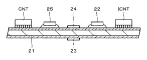
図7に示すように、多層プリント基板21上にコントロールボックスICNTを構成するMPU(MicroProcessing Unit)、非接触ICカード方式のリーダー/ライター側のLSI(Large Scale Integrated Circuit :大規模集積回路) 22がマウントされている。さらに、プリント基板アンテナ23および24、非接触ICカード方式のカード側のLSI25、並びにモジュールコントローラCNTが多層プリント基板21上にマウントされている。
As shown in FIG. 7, an MPU (MicroProcessing Unit) constituting a control box ICNT on a multilayer printed
図8に概念的に示すように、非接触ICカード方式においては、リーダー/ライター部26のアンテナ23から例えば搬送波振幅が2〜13Vopで、変調度が10%程度のカード部27に対する送信信号が形成される。送信信号がアンテナ23からカード部27のアンテナ24に送信される。アンテナ24において、受信された信号は、例えば搬送波振幅が2〜13Vopで、変調度が10%程度の高周波信号である。受信した信号を平滑化することによって、カード部27における電源が形成される。カード部27における消費電力は、充分小さいものである。
As conceptually shown in FIG. 8, in the non-contact IC card system, a transmission signal from the
プリント基板アンテナの一例について説明する。アンテナが導電パターンとして形成される多層プリント基板21としては、図9Aに示すように、4個の配線層LY1〜LY4を有する4層プリント基板が使用される。または図9Bに示すように、2個の配線層LY11、LY12を有する2層プリント基板が使用される。
An example of the printed circuit board antenna will be described. As the multilayer printed
図10Aに示すように、1次側(リーダー/ライター側)のアンテナ23が渦巻き状パターン31a、直線状パターン31bおよび直線状パターン31cによって形成される。4層プリント基板の第4の配線層LY4上に渦巻き状のパターン31aが形成され、パターン31aの中心部の端部がランドおよびスルーホールを介して第3の配線層LY3のランド32aに接続される。ランド32aからランド32bの間に直線状のパターン31bが形成される。ランド32bがスルーホールおよび第3の配線層LY3のランドを介して直線状のパターン31cに接続される。パターン31aおよび31cの端部が図示しないコネクタに接続される。
As shown in FIG. 10A, the primary side (reader / writer side)
図10Bに示すように、2次側(カード側)のアンテナ24が渦巻き状パターン41a、直線状パターン41b、直線状パターン41cおよび直線状パターン41dによって形成される。コネクタ(図示しない)と一端が接続された渦巻き状のパターン41aが4層プリント基板の第1の配線層LY1に形成される。ランド42a、スルーホールおよび第2の配線層LY2のランドを介して直線状のパターン41bと接続される。パターン41bの一端がランド42b、スルーホールを介して第1の配線層LY1のランドと接続される。直線状のパターン41cの一端がこの第1の配線層LY1のランドと接続される。直線状のパターン41cの他端がコネクタ(図示せず)と接続される。さらに、渦巻き状のパターン41aと接続されたランド42cに対して直線状のパターン41dの一端が接続される。直線状のパターン41dの他端が基準電位点に接続される。
As shown in FIG. 10B, the secondary (card side)
パターンが交差する場合には、異なる配線層のパターンによってプリント基板アンテナが構成されている。異なる配線層間を接続するために、スルーホールとランドが使用される。その結果、第4の配線層に図10Aに示すように、不要なランド32c、32dが発生し、第1の配線層に不要なランド42dが発生する。
When the patterns intersect, the printed circuit board antenna is constituted by patterns of different wiring layers. Through holes and lands are used to connect different wiring layers. As a result, as shown in FIG. 10A,
上述したパターンをプリント基板の他の配線層に形成するのに代えて、ジャンパー線を使用するようにしても良い。すなわち、図10Aにおけるパターン31b、並びに図10Bにおけるパターン41bおよび41dの代わりにジャンパー線が使用される。この場合には、2層プリント基板を使用でき、スルーホールを形成することが不要となり、不要なランドが発生することを防止することができる。スルーホールを形成しないことによって、プリント基板の絶縁耐圧をより高くすることが可能となる。
Instead of forming the above-mentioned pattern on the other wiring layer of the printed board, jumper wires may be used. That is, jumper lines are used instead of the
本開示の絶縁部は、1次側アンテナと2次側アンテナとの間の絶縁をプリント基板によって行っている。したがって、本開示の絶縁部においては、直流絶縁電圧として1000V以上が可能となる。さらに、双方向通信および電力伝送が可能な利点があり、コストを低くすることができる。 The insulation part of this indication performs insulation between a primary side antenna and a secondary side antenna with a printed circuit board. Therefore, in the insulating part of the present disclosure, a DC insulation voltage of 1000 V or more is possible. Furthermore, there is an advantage that bidirectional communication and power transmission are possible, and the cost can be reduced.
「セルバランスについて」
本開示では、上述した複数の蓄電モジュールMOD1〜MODn間の電圧バランス(以下、単にモジュールバランスと称する)を制御するものである。すなわち、モジュール間バランスの制御によって、各蓄電モジュールの出力電圧が均一化される。通常、各蓄電モジュールには、多数の電池セルが含まれているので、蓄電モジュール内の電池セル間の電圧バランス(以下、単にセルバランスと称する)に比較して蓄電モジュール間のバラツキが大きくなる。したがって、蓄電モジュール内のセルバランスの制御を行うにしても、モジュールバランス制御を行うことが有意義である。
“About Cell Balance”
In the present disclosure, the voltage balance between the plurality of power storage modules MOD1 to MODn (hereinafter simply referred to as module balance) is controlled. That is, the output voltage of each power storage module is made uniform by controlling the balance between modules. Normally, since each power storage module includes a large number of battery cells, the variation between the power storage modules is larger than the voltage balance between the battery cells in the power storage module (hereinafter simply referred to as cell balance). . Therefore, even if the cell balance in the power storage module is controlled, it is meaningful to perform the module balance control.
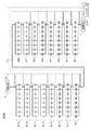
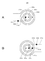
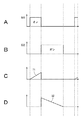
本開示の説明に先立って一般的なセルバランス制御について説明する。図11に示すように、3個の電池セルBT1、BT2、BT3間のセルバランスを検討する。最初は、図11Aに示すように、全ての電池セルが満充電されているものとする。次に、図11Bに示すように、電池セルが放電して放電量にバラツキが発生し、電池セルBT1の電圧が破線で示す使用下限電圧に達したとする。電池セル間のバラツキによって、他の電池セルBT2およびBT3は、未だ使用下限電圧には到達していない。例えば自己放電量の相違が電池セル間の放電量のバラツキの原因である。 Prior to the description of the present disclosure, general cell balance control will be described. As shown in FIG. 11, the cell balance between the three battery cells BT1, BT2, and BT3 is examined. Initially, as shown in FIG. 11A, it is assumed that all the battery cells are fully charged. Next, as illustrated in FIG. 11B, it is assumed that the battery cells are discharged and variations in the discharge amount occur, and the voltage of the battery cell BT1 reaches the use lower limit voltage indicated by a broken line. Due to the variation between the battery cells, the other battery cells BT2 and BT3 have not yet reached the use lower limit voltage. For example, the difference in self-discharge amount is a cause of variation in discharge amount between battery cells.
この状態で充電を開始すると、電池セルBT1の電圧が使用下限電圧に達した時点が残っている容量が最も多い電池セルBT2が最初に満容量に達する。この時点では、図11Cに示すように、電池セルBT1は、満充電まで充電されない。したがって、満充電であれば、放電量C1を放電できたのが、放電量C2に放電できる量が減少してしまう。 When charging is started in this state, the battery cell BT2 having the largest remaining capacity at the time when the voltage of the battery cell BT1 reaches the use lower limit voltage first reaches the full capacity. At this time, as shown in FIG. 11C, the battery cell BT1 is not charged until it is fully charged. Therefore, if the battery is fully charged, the discharge amount C1 can be discharged, but the amount that can be discharged to the discharge amount C2 is reduced.
この問題を解決するために、図12Aおよび図12Bに示すように、電池セルBT1が使用下限電圧に到達した時点で最も容量が残っている(最高電位)電池セルBT2から他の容量が最も少ない(最低電位)電池セルBT1に電力を移して残っている容量をほぼ等しいものとする。そして、電池セルBT1、BT2およびBT3を充電することによって、3個の電池セルをほぼ満充電電圧まで充電できる。実際には、複数回の処理を繰り返し行うようになされる。 In order to solve this problem, as shown in FIGS. 12A and 12B, when the battery cell BT1 reaches the use lower limit voltage, the capacity remains most (highest potential), and the other capacity is the smallest from the battery cell BT2. (Minimum potential) The power remaining in the battery cell BT1 is approximately equal. Then, by charging the battery cells BT1, BT2, and BT3, it is possible to charge the three battery cells to a substantially full charge voltage. Actually, the processing is repeated a plurality of times.
このような制御は、アクティブボトムセルバランス制御と称される。ボトムセルバランス制御によって放電できる量の減少を防止することができる。図12Aに示す状態で、最も電位の低い電池セルBT1と電位を合わせるように、電池セルBT2およびBT3を放電する方式は、パッシブボトムセルバランス制御と称される。パッシブ方式に比較してアクティブ方式の方が容量を有効に利用することができるので好ましい。 Such control is referred to as active bottom cell balance control. It is possible to prevent a decrease in the amount that can be discharged by the bottom cell balance control. In the state shown in FIG. 12A, the method of discharging the battery cells BT2 and BT3 so as to match the potential with the battery cell BT1 having the lowest potential is called passive bottom cell balance control. The active method is preferable because the capacity can be used more effectively than the passive method.
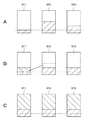
図13および図14を参照してアクティブトップバランス制御について説明する。最初は、図13Aに示すように、全ての電池セルが満充電されているものとする。次に、図13Bに示すように、電池セルが放電したとする。 The active top balance control will be described with reference to FIG. 13 and FIG. Initially, as shown in FIG. 13A, it is assumed that all the battery cells are fully charged. Next, as shown in FIG. 13B, it is assumed that the battery cell is discharged.
そして充電を開始すると、図13Cに示すように、電池セルBT2の電圧が最初に使用上限電圧に達する。この時点では、電池セルBT1およびBT3の電圧は、使用上限電圧まで達していない。したがって、充電量C11(図13A)に対して、充電量がC12で示すように減少してしまう。 When charging is started, as shown in FIG. 13C, the voltage of the battery cell BT2 first reaches the use upper limit voltage. At this time, the voltages of the battery cells BT1 and BT3 have not reached the use upper limit voltage. Therefore, the charge amount decreases as indicated by C12 with respect to the charge amount C11 (FIG. 13A).
この問題を解決するために、図14Aおよび図14Bに示すように、電池セルBT2が使用上限電圧に到達した時点で最も容量が多い(最高電位)電池セルBT2から他の容量が最も少ない(最低電位)電池セルBT1に電力を移して残っている容量をほぼ等しいものとする。そして、電池セルBT1、BT2およびBT3を充電することによって、3個の電池セルをほぼ満充電電圧まで充電できる。実際には、複数回の処理を繰り返し行うようになされる。 In order to solve this problem, as shown in FIG. 14A and FIG. 14B, when the battery cell BT2 reaches the upper limit voltage, the battery cell BT2 has the highest capacity (highest potential) and the other capacity is the lowest (lowest). Potential) It is assumed that the power remaining in the battery cell BT1 is approximately equal to the remaining capacity. Then, by charging the battery cells BT1, BT2, and BT3, it is possible to charge the three battery cells to a substantially full charge voltage. Actually, the processing is repeated a plurality of times.
このような制御は、アクティブトップセルバランス制御と称される。トップセルバランス制御によって充電できる量の減少を防止することができる。図14Aに示す状態で、最も電位の低い電池セルBT1と電位を合わせるように、電池セルBT2およびBT3を放電する方式は、パッシブトップセルバランス制御と称される。パッシブ方式に比較してアクティブ方式の方が容量を有効に利用することができるので好ましい。 Such control is referred to as active top cell balance control. The amount of charge that can be charged can be prevented by the top cell balance control. In the state shown in FIG. 14A, the method of discharging the battery cells BT2 and BT3 so as to match the potential with the battery cell BT1 having the lowest potential is called passive top cell balance control. The active method is preferable because the capacity can be used more effectively than the passive method.
「従来のセルバランス制御回路」
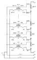
図15および図16を参照してフライバックトランスを使用する従来のアクティブボトムセルバランス回路の一例について説明する。各電池セルの正極および負極と1次側コイルW1〜W6の両端が接続される。6個の電池セルBT1〜BT6の直列接続の正極および負極と2次側コイルW0の両端が接続される。さらに、共通の磁芯Mが設けられている。さらに、2次側コイルW0と直列に2次側スイッチS0が接続され、1次側コイルW1〜W6のそれぞれと直列に1次側スイッチS1〜S6が接続される。スイッチS0〜S6は、例えばMOS(Metal Oxide Semiconductor)FETによって構成される。
"Conventional cell balance control circuit"
An example of a conventional active bottom cell balance circuit using a flyback transformer will be described with reference to FIGS. The positive and negative electrodes of each battery cell are connected to both ends of primary coils W1 to W6. The positive and negative electrodes of the six battery cells BT1 to BT6 connected in series are connected to both ends of the secondary coil W0. Furthermore, a common magnetic core M is provided. Further, the secondary side switch S0 is connected in series with the secondary side coil W0, and the primary side switches S1 to S6 are connected in series with each of the primary side coils W1 to W6. The switches S0 to S6 are configured by, for example, a MOS (Metal Oxide Semiconductor) FET.
図16は、図15に示すアクティブボトムセルバランス回路の動作のタイミングチャートである。一例として、図示しないモニタ部によって電池セルBT1〜BT6の各電圧が検出され、電池セルBT2の電圧が最も低いと検出される。この場合では、他の電池セルから電池セルBT2に対して電力が移動される。まず、図15Aおよび図16Aに示すように、スイッチS0がオンとされ、コイルW0に図16Cに示すように、電流I1が流れ、磁芯Mが磁化される。 FIG. 16 is a timing chart of the operation of the active bottom cell balance circuit shown in FIG. As an example, each voltage of the battery cells BT1 to BT6 is detected by a monitor unit (not shown), and it is detected that the voltage of the battery cell BT2 is the lowest. In this case, power is transferred from another battery cell to battery cell BT2. First, as shown in FIGS. 15A and 16A, the switch S0 is turned on, the current I1 flows through the coil W0 as shown in FIG. 16C, and the magnetic core M is magnetized.
次に、図15Bおよび図16Bに示すように、コイルW2と直列接続された1次側スイッチS2がオンされると共に、図16Aに示すように、2次側スイッチS0がオフされる。磁芯Mの電磁エネルギーが放出され、1次側コイルW2に図16Dに示すように、電流I2が流れる。この電流I2が電池セルBT2に流れ、電池セルBT2が充電される。 Next, as shown in FIGS. 15B and 16B, the primary side switch S2 connected in series with the coil W2 is turned on, and the secondary side switch S0 is turned off as shown in FIG. 16A. The electromagnetic energy of the magnetic core M is released, and a current I2 flows through the primary coil W2 as shown in FIG. 16D. This current I2 flows into the battery cell BT2, and the battery cell BT2 is charged.
その後、1次側スイッチS2が図16Bに示すように、オフとされる。さらに、所定時間のポーズ時間が後に続く。以上の2次側スイッチS0のオン期間、1次側スイッチS2のオン期間およびポーズ期間がサイクル周期とされて、動作が繰り返される。 Thereafter, the primary side switch S2 is turned off as shown in FIG. 16B. Further, a predetermined pause time follows. The above-described ON period of the secondary side switch S0, the ON period of the primary side switch S2, and the pause period are set as cycle periods, and the operation is repeated.
図17および図18を参照して従来のアクティブトップセルバランス回路の一例について説明する。各電池セルの正極および負極と1次側コイルW1〜W6の両端が接続される。6個の電池セルBT1〜BT6の直列接続の正極および負極と2次側コイルW0の両端が接続される。さらに、共通の磁芯Mが設けられている。さらに、1次側コイルW1〜W6のそれぞれと直列に1次側スイッチS1〜S6が接続され、2次側コイルW0と直列に2次側スイッチS0が接続され、スイッチS0〜S6は、例えばMOSFETによって構成される。 An example of a conventional active top cell balance circuit will be described with reference to FIGS. The positive and negative electrodes of each battery cell are connected to both ends of primary coils W1 to W6. The positive and negative electrodes of the six battery cells BT1 to BT6 connected in series are connected to both ends of the secondary coil W0. Furthermore, a common magnetic core M is provided. Further, the primary side switches S1 to S6 are connected in series with each of the primary side coils W1 to W6, the secondary side switch S0 is connected in series with the secondary side coil W0, and the switches S0 to S6 are, for example, MOSFETs Consists of.
図18は、図17に示すアクティブトップセルバランス回路の動作のタイミングチャートである。一例として、図示しないモニタ部によって電池セルBT1〜BT6の各電圧が検出され、電池セルBT5の電圧が最も高いと検出される。この場合では、電池セルBT5から他の電池セルに対して電力が移動される。まず、図17Aおよび図18Bに示すように、スイッチS5がオンとされ、コイルW5に図18Dに示すように、電流I1が流れ、磁芯Mが磁化される。 FIG. 18 is a timing chart of the operation of the active top cell balance circuit shown in FIG. As an example, each voltage of the battery cells BT1 to BT6 is detected by a monitor unit (not shown), and it is detected that the voltage of the battery cell BT5 is the highest. In this case, electric power is transferred from the battery cell BT5 to the other battery cells. First, as shown in FIGS. 17A and 18B, the switch S5 is turned on, the current I1 flows through the coil W5 as shown in FIG. 18D, and the magnetic core M is magnetized.
次に、図17Bおよび図18Aに示すように、2次側スイッチS0がオンされると共に、図18Bに示すように、12側スイッチS5がオフされる。磁芯Mの電磁エネルギーによって、2次側コイルW0に図18Cに示すように、電流I2が流れる。この電流I2が電池セルBT1〜BT6の直列接続に流れ、各電池セルに電力が分配される。 Next, as shown in FIGS. 17B and 18A, the secondary side switch S0 is turned on, and as shown in FIG. 18B, the 12 side switch S5 is turned off. As shown in FIG. 18C, the current I2 flows through the secondary coil W0 by the electromagnetic energy of the magnetic core M. This current I2 flows in series connection of battery cells BT1-BT6, and electric power is distributed to each battery cell.
その後、2次側スイッチS0が図18Aに示すように、オフとされる。さらに、所定時間のポーズ時間が後に続く。以上の1次側スイッチS5のオン期間、2次側スイッチS0のオン期間およびポーズ期間がサイクル周期とされて、動作が繰り返される。 Thereafter, the secondary side switch S0 is turned off as shown in FIG. 18A. Further, a predetermined pause time follows. The above-described ON period of the primary switch S5, the ON period of the secondary switch S0, and the pause period are set as cycle periods, and the operation is repeated.
「従来のモジュール間バランス回路」
上述した従来のバランス回路は、電池セルに関するものであり、図1〜図6を参照して説明したモジュール間バランスに適用した場合、問題が生じる。なお、モジュール間バランスは、各蓄電モジュール内の複数の電池セルまたは複数の電池ブロックからなる電池部の電圧のバランスのことである。通常、モジュール間アンバランスの方がモジュール内のアンバランスに比して大きな値となる。蓄電モジュール毎のバランス制御を行った結果として、モジュール間のアンバランスを解消することも可能であるが、処理に要する時間が長くなる。但し、モジュール間バランス制御と上述した従来のセルバランス制御を併用しても良い。この場合では、一例として、モジュール間バランス制御が先になされ、その後、モジュール内のバランス制御がなされる。
"Conventional balance circuit between modules"
The conventional balance circuit described above relates to a battery cell, and a problem occurs when applied to the inter-module balance described with reference to FIGS. The inter-module balance is the voltage balance of the battery unit composed of a plurality of battery cells or a plurality of battery blocks in each power storage module. Usually, the imbalance between modules is larger than the imbalance within the module. As a result of performing balance control for each power storage module, it is possible to eliminate imbalance between modules, but the time required for processing becomes longer. However, the inter-module balance control and the conventional cell balance control described above may be used in combination. In this case, as an example, inter-module balance control is performed first, and then balance control within the module is performed.
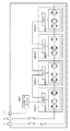
従来のセルバランス回路をそのままアクティブモジュール間バランス回路に適用した構成を図19に示す。例えば14個のモジュール間のバランス制御がなされる。電池ブロックグループBB1〜BB14が直列接続される。各電池ブロックグループは、8個の電池セルが並列接続され、8個の電池セルの並列接続(電池ブロック)が16個直列接続された構成(所謂(8P16S))を有する。例えば一つの電池ブロックグループが(3.2V×16=51.2V)の電圧を発生する。したがって、14個の電池ブロックグループBB1〜BB14が直列接続は、(51.2V×14=716.8V)の電圧を発生する。 FIG. 19 shows a configuration in which a conventional cell balance circuit is directly applied to an active module balance circuit. For example, balance control between 14 modules is performed. Battery block groups BB1 to BB14 are connected in series. Each battery block group has a configuration (so-called (8P16S)) in which eight battery cells are connected in parallel, and sixteen parallel connections (battery blocks) of eight battery cells are connected in series. For example, one battery block group generates a voltage of (3.2 V × 16 = 51.2 V). Accordingly, 14 battery block groups BB1 to BB14 are connected in series to generate a voltage of (51.2V × 14 = 716.8V).
14個の電池ブロックグループの直列接続の正極側および負極側と2次側コイルW0の両端が接続される。さらに、共通の磁芯Mが設けられている。さらに、2次側コイルW0と直列に2次側スイッチS0が接続され、1次側コイルW1〜W14のそれぞれと直列に1次側スイッチS1〜S14が接続される。スイッチS0〜S14は、例えばMOSFETによって構成される。 The positive and negative sides of the 14 battery block groups connected in series are connected to both ends of the secondary coil W0. Furthermore, a common magnetic core M is provided. Further, the secondary side switch S0 is connected in series with the secondary side coil W0, and the primary side switches S1 to S14 are connected in series with each of the primary side coils W1 to W14. The switches S0 to S14 are configured by MOSFETs, for example.
図19の構成におけるアクティブボトムセルバランス動作は、スイッチS0をオンとし、2次側コイルW0に流れる電流によって磁芯Mが磁化される。次に、電圧が最も低い蓄電モジュールの1次側スイッチをオンとし、1次側コイルに伝えられた電磁エネルギーによって当該蓄電モジュールの電池ブロックグループを充電する。一例として、電池ブロックグループBB2の電圧が32.0Vであり、他の電池ブロックグループの電圧が32.6Vである場合には、2次側スイッチS0を所定時間オンとした後に、スイッチS0がオフされると共に、電池ブロックグループBB2の1次側スイッチS2がオンとされる。1次側コイルW2を流れる電流によって、電池ブロックグループBB2が充電される。 In the active bottom cell balance operation in the configuration of FIG. 19, the switch S0 is turned on, and the magnetic core M is magnetized by the current flowing through the secondary coil W0. Next, the primary side switch of the power storage module having the lowest voltage is turned on, and the battery block group of the power storage module is charged by the electromagnetic energy transmitted to the primary side coil. As an example, when the voltage of the battery block group BB2 is 32.0V and the voltage of the other battery block group is 32.6V, the switch S0 is turned off after the secondary side switch S0 is turned on for a predetermined time. At the same time, the primary side switch S2 of the battery block group BB2 is turned on. Battery block group BB2 is charged by the current flowing through primary coil W2.
図19の構成におけるアクティブトップセルバランス動作は、電圧が最も高い電池ブロックグループの1次側コイルに接続されたスイッチをオンとし、次に、当該スイッチをオフとすると共に、スイッチS0をオンとし、2次側コイルW0に電流を流し、電池ブロックグループBB1〜BB14を充電する。一例として、電池ブロックグループBB2の電圧が56.5Vであり、他の電池ブロックグループの電圧が55.9Vである場合には、1次側スイッチS2を所定時間オンとした後に、スイッチS2がオフされると共に、2次側スイッチS0がオンとされる。2次側コイルW0を流れる電流によって、電池ブロックグループBB1〜BB14が充電される。 In the active top cell balance operation in the configuration of FIG. 19, the switch connected to the primary coil of the battery block group having the highest voltage is turned on, and then the switch is turned off and the switch S0 is turned on. A current is passed through the secondary coil W0 to charge the battery block groups BB1 to BB14. As an example, when the voltage of the battery block group BB2 is 56.5V and the voltage of the other battery block group is 55.9V, the switch S2 is turned off after the primary side switch S2 is turned on for a predetermined time. At the same time, the secondary side switch S0 is turned on. Battery block groups BB1 to BB14 are charged by the current flowing through secondary coil W0.
図19の構成では、トランスの磁芯Mが共通であるので、複数例えば14個の蓄電モジュールを別々のケースに収納して構成することが困難である。この場合には、磁芯、コイルおよびスイッチからなるトランス部分を14個の蓄電モジュールとは別のケースに収納してトランス装置を構成し、このトランス装置を中心とするスター状に14個の蓄電モジュールが接続される。かかるスター状の構成は、蓄電モジュール数が多いとスター状の配線が複雑となる問題がある。 In the configuration of FIG. 19, since the transformer core M is common, it is difficult to configure a plurality of, for example, 14 power storage modules in different cases. In this case, a transformer unit is configured by housing a transformer portion including a magnetic core, a coil, and a switch in a case different from the 14 power storage modules, and the 14 power storages are formed in a star shape centering on the transformer device. Module is connected. Such a star-shaped configuration has a problem that the star-shaped wiring becomes complicated when the number of power storage modules is large.
「従来のモジュール間バランス回路の問題点」
図19の構成では、2次側コイルW0およびスイッチS0の直列回路に対して、直列接続された14個の電池ブロックグループによって716.8Vの電圧が印加される。実際に使用する場合に必要な耐圧は、印加電圧の3倍程度とされるので、スイッチS0を構成するFET等の半導体スイッチ素子の耐圧が2000V以上となる。このような耐圧の半導体スイッチ素子を必要とする図19の構成は、実現が困難なものである。
“Problems of the conventional balance circuit between modules”
In the configuration of FIG. 19, a voltage of 716.8 V is applied to the series circuit of the secondary coil W0 and the switch S0 by 14 battery block groups connected in series. Since the withstand voltage required for actual use is about three times the applied voltage, the withstand voltage of a semiconductor switch element such as an FET constituting the switch S0 is 2000 V or more. The configuration of FIG. 19 that requires such a withstand voltage semiconductor switch element is difficult to realize.
図20に示すように、磁芯Mを14個の磁芯M1〜M14に分割し、2次側コイルW0を14個の2次側コイルW01〜W014に分割する。このようにすれば、14個の蓄電モジュールを分離してケース収納することができる。図20の構成では、1次側スイッチS01〜S014のそれぞれに対して716.8Vの電圧が印加される。しかしながら、図20の構成は、フライバックトランスが別々に構成され、その1次側および2次側のスイッチも各コイルにそれぞれ接続されて独立にスイッチング動作を制御することが可能である。したがって、後述するように、複数の電池ブロックグループから並行して電力を取り出したり、複数の電池ブロックグループに対して並行して電力を供給する制御が可能となる。しかも、スイッチング動作のオン期間の長さを制御することによって、電力量を制御することができる。 As shown in FIG. 20, the magnetic core M is divided into 14 magnetic cores M1 to M14, and the secondary coil W0 is divided into 14 secondary coils W01 to W014. In this way, the 14 power storage modules can be separated and housed in a case. In the configuration of FIG. 20, a voltage of 716.8 V is applied to each of the primary side switches S01 to S014. However, in the configuration of FIG. 20, the flyback transformer is configured separately, and the primary side and secondary side switches are also connected to the respective coils, and the switching operation can be controlled independently. Therefore, as described later, it is possible to control power to be taken out from a plurality of battery block groups in parallel or to supply power to a plurality of battery block groups in parallel. In addition, the amount of power can be controlled by controlling the length of the on period of the switching operation.
「先に提案されているモジュール間バランス回路」
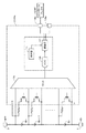
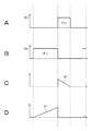
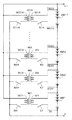
図21に示すように、先に提案されている構成(特開2013−051856号公報参照)では、1次側コイルW1と、2次側コイルW01と、磁芯M1とによって、フライバックトランスT1が構成される。1次側コイルW1とスイッチS1が直列接続され、2次側コイルW01とスイッチS01が直列接続される。同様に、1次側コイルW2〜W14と、2次側コイルW02〜W014と、磁芯M2〜M14と、によって、フライバックトランスT2〜T14が構成される。1次側コイルW2〜W14とスイッチS2〜S14が直列に接続される。2次側コイルW02〜W014とスイッチS02〜S014とが直列に接続される。
"Proposed inter-module balance circuit"
As shown in FIG. 21, in the previously proposed configuration (see Japanese Patent Application Laid-Open No. 2013-051856), a flyback transformer T1 is constituted by a primary coil W1, a secondary coil W01, and a magnetic core M1. Is configured. The primary coil W1 and the switch S1 are connected in series, and the secondary coil W01 and the switch S01 are connected in series. Similarly, flyback transformers T2 to T14 are configured by the primary side coils W2 to W14, the secondary side coils W02 to W014, and the magnetic cores M2 to M14. Primary coils W2-W14 and switches S2-S14 are connected in series. Secondary coils W02 to W014 and switches S02 to S014 are connected in series.
フライバックトランスT1の1次側コイルW1とスイッチS1の直列回路が蓄電モジュールの電池ブロックグループBB1の正側および負側と接続される。他の1次側コイルW2〜W14とスイッチS2〜S14のそれぞれの直列回路が蓄電モジュールの電池ブロックグループBB2〜BB14の正側および負側と接続される。 A series circuit of primary side coil W1 of flyback transformer T1 and switch S1 is connected to the positive side and negative side of battery block group BB1 of the power storage module. Series circuits of other primary coils W2 to W14 and switches S2 to S14 are connected to the positive side and the negative side of battery block groups BB2 to BB14 of the storage module.
蓄電素子51が設けられており、蓄電素子51によって共通電源電圧CVが発生する。共通電源電圧CVは、電池ブロックグループの直列接続の合計の電圧716.8Vよりも低い電圧とされる。好ましくは、2次側スイッチの耐圧のほぼ1/3の電圧以下に設定される。例えば電池ブロックグループの単位電圧(51.2V)とほぼ等しい値に設定される。共通電源電圧CVの電位は、トータルの放電電流と、トータルの充電電流とを制御することで、溢れず、枯渇せず、所望の電圧になるように制御される。
A
蓄電素子51は、電池、コンデンサ等である。蓄電素子51によって、一方の共通電源ラインCL+が共通電源電圧CVとされ、他方の共通電源ラインCL−が0Vとされる。他方の共通電源ラインCL−は、複数の蓄電モジュールの電池ブロックグループの直列接続の電源(V−)とは接続されていない別の電源とされている。但し、共通電源ラインCL−を電源V−に接続しても良い。分割された2次側コイルW01〜W014の一端が共通電源ラインCL+にそれぞれ接続され、分割された2次側コイルW01〜W014の他端がスイッチS01〜S014を通じて共通電源ラインCL−にそれぞれ接続される。
The
スイッチS0〜S14並びにスイッチS01〜S014は、例えばMOSFETによって構成される。図22に示すように、例えばフライバックトランスT1のスイッチS01は、MOSFETQ01とそのドレイン・ソース間に接続されたダイオードD01とによって構成され、スイッチS1は、MOSFETQ1とそのドレイン・ソース間に接続されたダイオードD1とによって構成される。スイッチのオン/オフは、コントロールボックスICNTの制御部からのコントロール信号によって制御される。コントロールボックスICNTは、各蓄電モジュールのモジュールコントローラCNTからの電圧の監視結果の情報を受け取って、コントロール信号(パルス信号)を生成する。なお、MOSFET以外に、IGBT((Insulated Gate Bipolar Transistor):絶縁ゲートバイポーラトランジスタ)等の半導体スイッチ素子を使用しても良い。なお、スイッチ(MOSFETとそのドレイン・ソース間に接続されたダイオードで構成される)は、ソース→ドレイン方向に流れる電流に対しては、コントロール信号が無くてもダイオードを通じて自動的に電流が流れる(自動的スイッチのオン)。 The switches S0 to S14 and the switches S01 to S014 are configured by, for example, MOSFETs. As shown in FIG. 22, for example, the switch S01 of the flyback transformer T1 is configured by a MOSFET Q01 and a diode D01 connected between its drain and source, and the switch S1 is connected between the MOSFET Q1 and its drain and source. It is comprised by the diode D1. The on / off of the switch is controlled by a control signal from the control unit of the control box ICNT. The control box ICNT receives the voltage monitoring result information from the module controller CNT of each power storage module, and generates a control signal (pulse signal). In addition to the MOSFET, a semiconductor switch element such as an IGBT (Insulated Gate Bipolar Transistor) may be used. Note that the switch (consisting of a MOSFET and a diode connected between its drain and source) automatically flows through the diode even if there is no control signal for the current flowing in the source-to-drain direction ( Automatic switch on).
2次側コイルW01〜W014とスイッチS01〜S014の直列回路には、共通電源電圧CVが印加される。例えば1次側コイルおよびスイッチに印加される電圧と同様の電圧(51.2V)に共通電源電圧CVを設定することによって、2次側スイッチS01〜S014の耐圧を154V程度とすることができる。このような耐圧は、2次側スイッチS01〜S014を構成する半導体スイッチにとってそれぼど高い値ではなく、モジュール間バランス回路を構成することが容易となる。 A common power supply voltage CV is applied to the series circuit of the secondary coils W01 to W014 and the switches S01 to S014. For example, by setting the common power supply voltage CV to the same voltage (51.2V) as the voltage applied to the primary side coil and the switch, the withstand voltage of the secondary side switches S01 to S014 can be set to about 154V. Such a withstand voltage is not very high for the semiconductor switches constituting the secondary side switches S01 to S014, and it is easy to configure an inter-module balance circuit.
フライバックトランスT1〜T14のそれぞれは、1次側コイルと2次側コイルの巻線比は、1と限定されないが、1次側と2次側とで位相が逆とされている。さらに、フライバックトランスT1〜T14は、双方向に電力を伝送することができる。したがって、1次側および2次側の表記は、便宜上のものであり、1次側から2次側への電力伝送、並びに2次側から1次側への電力伝送の何れも可能である。 In each of the flyback transformers T1 to T14, the winding ratio of the primary side coil and the secondary side coil is not limited to 1, but the phase is reversed between the primary side and the secondary side. Further, the flyback transformers T1 to T14 can transmit power in both directions. Therefore, the notation of the primary side and the secondary side is for convenience, and both power transmission from the primary side to the secondary side and power transmission from the secondary side to the primary side are possible.
フライバックトランスT1を例にとると、スイッチS1およびS01がオフの状態からスイッチS1がオンすると、コイルW1に電流が流れ、磁芯M1が磁化される。スイッチS1がオンの期間コイルW1には、時間と共に増大する電流が流れる。次に、スイッチS1をオフとし、スイッチS01をオンとすると、磁芯が磁化されているので、コイルW01には、スイッチS01を介して電流が流れる。この電流は、時間と共に減少する電流となる。他のフライバックトランスの動作も同様である。フライバックトランスは、結合インダクタとしての機能を有する。 Taking the flyback transformer T1 as an example, when the switch S1 is turned on from the state where the switches S1 and S01 are off, a current flows through the coil W1, and the magnetic core M1 is magnetized. While the switch S1 is on, a current that increases with time flows through the coil W1. Next, when the switch S1 is turned off and the switch S01 is turned on, since the magnetic core is magnetized, a current flows through the coil W01 via the switch S01. This current becomes a current that decreases with time. The operation of other flyback transformers is the same. The flyback transformer has a function as a coupled inductor.
図21の構成におけるアクティブボトムセルバランス動作では、1次側スイッチを制御することによって、最も電圧が高い電池ブロックグループから蓄電素子51に対して電力が移動される。さらに、2次側スイッチを制御することによって、電圧が最も低い蓄電モジュールの電池ブロックグループに対して電力が移動される。このように、本開示によるモジュール間バランス回路は、双方向フライバックトランスを2段介して電力を移動させる。
In the active bottom cell balance operation in the configuration of FIG. 21, power is transferred from the battery block group having the highest voltage to the
一例として、電池ブロックグループBB3の電圧が最も高く32.6Vであり、電池ブロックグループBB2の電圧が最も低く32.0Vである場合の動作を説明する。まず、スイッチS3がオンとされ、電池ブロックグループBB3を電源としてフライバックトランスT3の1次側コイルW3に電流が流れる。次に、スイッチS3がオフとされ、スイッチS03がオンとされる。電磁エネルギーによって、2次側コイルW03に電流が流れ、蓄電素子51が充電される。
As an example, an operation when the voltage of the battery block group BB3 is the highest and 32.6V and the voltage of the battery block group BB2 is the lowest and 32.0V will be described. First, the switch S3 is turned on, and a current flows through the primary coil W3 of the flyback transformer T3 using the battery block group BB3 as a power source. Next, the switch S3 is turned off and the switch S03 is turned on. Due to the electromagnetic energy, a current flows through the secondary coil W03, and the
次に、スイッチS03がオフとされると共に、スイッチS02がオンとされ、蓄電素子51によって、フライバックトランスT2の2次側コイルW02に電流が流れる。次に、スイッチS02がオフとされると共に、スイッチS2がオンとされ、1次側コイルW2に流れる電流によって、電池ブロックグループBB2が充電される。このようにして、アクティブボトムセルバランス動作がなされる。
Next, the switch S03 is turned off, the switch S02 is turned on, and a current flows through the secondary coil W02 of the flyback transformer T2 by the
図21の構成におけるアクティブトップセルバランス動作では、1次側スイッチを制御することによって、最も電圧が高い電池ブロックグループから蓄電素子51に対して電力が移動される。さらに、2次側スイッチを制御することによって、電圧が最も低い蓄電モジュールの電池ブロックグループに対して電力が移動される。このように、本開示によるモジュール間バランス回路は、双方向フライバックトランスを2段介して電力を移動させる。
In the active top cell balance operation in the configuration of FIG. 21, power is transferred from the battery block group having the highest voltage to the
一例として、電池ブロックグループBB3の電圧が最も高く56.5Vであり、電池ブロックグループBB2の電圧が最も低く55.9Vである場合の動作を説明する。まず、フライバックトランスT3のスイッチS3がオンとされ、電池ブロックグループBB3を電源として1次側コイルW3に電流が流れる。次に、スイッチS3がオフとされ、スイッチS03がオンとされる。電磁エネルギーによって、2次側コイルW03に電流が流れ、蓄電素子51が充電される。
As an example, an operation when the voltage of the battery block group BB3 is the highest and 56.5V and the voltage of the battery block group BB2 is the lowest and 55.9V will be described. First, the switch S3 of the flyback transformer T3 is turned on, and a current flows through the primary coil W3 using the battery block group BB3 as a power source. Next, the switch S3 is turned off and the switch S03 is turned on. Due to the electromagnetic energy, a current flows through the secondary coil W03, and the
次に、スイッチS03がオフとされると共に、フライバックトランスT2のスイッチS02がオンとされ、蓄電素子51によって、2次側コイルW02に電流が流れる。次に、スイッチS02がオフとされると共に、スイッチS2がオンとされ、1次側コイルW2に流れる電流によって、電池ブロックグループBB2が充電される。このようにして、アクティブトップセルバランス動作がなされる。
Next, the switch S03 is turned off, the switch S02 of the flyback transformer T2 is turned on, and a current flows through the secondary coil W02 by the
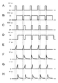
図23および図24を参照してアクティブトップセルバランス動作についてより詳細に説明する。一例として、図23に示すように、14個の蓄電モジュールのそれぞれの電池ブロックグループの電圧関係が蓄電モジュールMOD3の電池ブロックグループBB3の電圧が最も高く(例えば56.5V)であり、蓄電モジュールMOD2の電池ブロックグループBB2の電圧が最も低く(例えば55.9V)とする。さらに、図23に示すように、フライバックトランスT3のコイルW3を流れる電流をi1とし、コイルW03を流れる電流をi2と表記する。電流i1およびi2は、逆位相である。フライバックトランスT2のコイルW02を流れる電流をi3とし、コイルW2を流れる電流をi4と表記する。電流i3およびi4は、逆位相である。さらに、動作開始時に蓄電素子51が充分に充電されているものとする。
The active top cell balance operation will be described in more detail with reference to FIG. 23 and FIG. As an example, as shown in FIG. 23, the voltage relationship of the battery block groups of the 14 power storage modules is the highest in the voltage of the battery block group BB3 of the power storage module MOD3 (for example, 56.5 V), and the power storage module MOD2 The voltage of the battery block group BB2 is the lowest (for example, 55.9V). Furthermore, as shown in FIG. 23, the current flowing through the coil W3 of the flyback transformer T3 is denoted by i1, and the current flowing through the coil W03 is denoted by i2. Currents i1 and i2 are in antiphase. The current flowing through the coil W02 of the flyback transformer T2 is denoted by i3, and the current flowing through the coil W2 is denoted by i4. Currents i3 and i4 are in antiphase. Furthermore, it is assumed that the
図24のタイミングチャートに示すように、フライバックトランスT3を通じてなされる電力伝送と、フライバックトランスT2を通じてなされる電力伝送とが並行してなされる。まず、図24Aおよび図24Cに示すように、スイッチS3およびS02が同一の期間オンとされる。スイッチS3のオンによって、コイルW3に対して図24Eに示すように、徐々に増大する電流i1が流れる。スイッチS02のオンによって、コイルW02に対して図24Gに示すように、徐々に増大する電流i3が流れる。電流i3が蓄電素子51に対して放電方向に流れる。
As shown in the timing chart of FIG. 24, power transmission performed through the flyback transformer T3 and power transmission performed through the flyback transformer T2 are performed in parallel. First, as shown in FIGS. 24A and 24C, the switches S3 and S02 are turned on for the same period. When the switch S3 is turned on, a gradually increasing current i1 flows through the coil W3 as shown in FIG. 24E. When the switch S02 is turned on, a gradually increasing current i3 flows through the coil W02 as shown in FIG. 24G. The current i3 flows in the discharge direction with respect to the
次に、スイッチS3およびS02がオフとされ、図24Bおよび図24Dに示すように、スイッチS03およびS2が同一の期間オンとされる。スイッチS03のオンによって、コイルW03に対して図24Fに示すように、徐々に減少する電流i2が流れる。電流i2が蓄電素子51に対して充電方向に流れる。電流i2による蓄電素子51に対する充電によって、電池ブロックグループBB3から電力が蓄電素子51に移動される。
Next, the switches S3 and S02 are turned off, and as shown in FIGS. 24B and 24D, the switches S03 and S2 are turned on for the same period. When the switch S03 is turned on, a gradually decreasing current i2 flows through the coil W03 as shown in FIG. 24F. The current i2 flows in the charging direction with respect to the
スイッチS2のオンによって、コイルW2に対して図24Hに示すように、徐々に減少する電流i4が流れる。電流i4が電池ブロックグループBB2を充電する方向に流れる。電流i4による充電によって、蓄電素子51の電力が電池ブロックグループBB2に移動される。なお、実際の電力伝送は、1回のスイッチング動作ではなく、複数回のスイッチング動作によって、少しずつ電力を移動させるようになされる。スイッチング動作の周期は、10sec程度の長いものとされている。さらに、スイッチに対するパルス信号をパルス幅変調して、スイッチのオン期間を制御し、電力の移動量を所望のものに設定することができる。また、図24において、スイッチS3とS02は、同期した形で記述しているが、実際には、共通電源電圧CVは、ある程度の幅を許容することで、同期関係がなくても構わない。
When the switch S2 is turned on, a gradually decreasing current i4 flows through the coil W2, as shown in FIG. 24H. The current i4 flows in the direction of charging the battery block group BB2. By charging with the current i4, the electric power of the
上位コントローラとしてのコントロールボックスICNTは、各蓄電モジュールの電圧を監視しており、検出した蓄電モジュールの電池が互いに等しくなると、モジュール間バランス制御動作を停止するように制御する。そして、蓄電モジュールの電圧に差が生じた場合に、モジュール間バランス制御動作を開始するようになされる。図25に上述した先に提案されている蓄電装置の動作における電荷の移動を示す。 The control box ICNT as the host controller monitors the voltage of each power storage module, and controls the inter-module balance control operation to stop when the detected batteries of the power storage modules become equal to each other. And when a difference arises in the voltage of an electrical storage module, the balance control operation between modules is started. FIG. 25 shows charge transfer in the operation of the previously proposed power storage device.
「本開示の一実施の形態のモジュール間バランス回路」
本開示の一実施の形態は、先に提案されている蓄電装置と同様の構成を有するが、電荷の移動の周期をより短いものとし、電荷移動のためのスイッチングの回数をより多くするものである。すなわち、先に提案されている蓄電装置では、電池ブロックグループを構成するセルが上述したような正極材料としてオリビン構造を有する正極活物質を含有するものを使用する場合、モジュール間バランス制御が良好になされないおそれがある。
"Inter-module balance circuit according to an embodiment of the present disclosure"
One embodiment of the present disclosure has a configuration similar to that of the previously proposed power storage device, but has a shorter charge transfer period and more switching times for charge transfer. is there. That is, in the previously proposed power storage device, when the cells constituting the battery block group use the positive electrode material containing the positive electrode active material having the olivine structure as described above, the inter-module balance control is good. May not be done.
図26〜図29を参照して本開示の一実施の形態の動作の一例について説明する。図26は、図23の接続構成と同一のものである。対応する部分に対しては、同一の参照符号を付して示す。一例として、電池ブロックグループBB3の電圧が最も高く56.5Vであり、電池ブロックグループBB2の電圧が最も低く55.9Vである場合の動作を説明する。まず、フライバックトランスT3のスイッチS3がオンとされ、電池ブロックグループBB3を電源として1次側コイルW3に電流が流れる。次に、スイッチS3がオフとされ、スイッチS03がオンとされる。電磁エネルギーによって、2次側コイルW03に電流が流れ、蓄電素子51が充電される。
An example of the operation of the embodiment of the present disclosure will be described with reference to FIGS. FIG. 26 is the same as the connection configuration of FIG. Corresponding portions are denoted by the same reference numerals. As an example, an operation when the voltage of the battery block group BB3 is the highest and 56.5V and the voltage of the battery block group BB2 is the lowest and 55.9V will be described. First, the switch S3 of the flyback transformer T3 is turned on, and a current flows through the primary coil W3 using the battery block group BB3 as a power source. Next, the switch S3 is turned off and the switch S03 is turned on. Due to the electromagnetic energy, a current flows through the secondary coil W03, and the
次に、スイッチS03がオフとされると共に、フライバックトランスT2のスイッチS02がオンとされ、蓄電素子51によって、2次側コイルW02に電流が流れる。次に、スイッチS02がオフとされると共に、スイッチS2がオンとされ、1次側コイルW2に流れる電流によって、電池ブロックグループBB2が充電される。このようにして、アクティブトップセルバランス動作がなされる。
Next, the switch S03 is turned off, the switch S02 of the flyback transformer T2 is turned on, and a current flows through the secondary coil W02 by the
図26および図27を参照してアクティブトップセルバランス動作についてより詳細に説明する。一例として、図26に示すように、14個の蓄電モジュールのそれぞれの電池ブロックグループの電圧関係が蓄電モジュールMOD3の電池ブロックグループBB3の電圧が最も高く(例えば56.5V)であり、蓄電モジュールMOD2の電池ブロックグループBB2の電圧が最も低く(例えば55.9V)とする。さらに、図26に示すように、フライバックトランスT3のコイルW3を流れる電流をi1とし、コイルW03を流れる電流をi2と表記する。電流i1およびi2は、逆位相である。フライバックトランスT2のコイルW02を流れる電流をi3とし、コイルW2を流れる電流をi4と表記する。電流i3およびi4は、逆位相である。さらに、動作開始時に蓄電素子51が充分に充電されているものとする。
The active top cell balance operation will be described in more detail with reference to FIGS. As an example, as shown in FIG. 26, the battery block group BB3 of the power storage module MOD3 has the highest voltage relationship (for example, 56.5 V) in the battery block group of each of the 14 power storage modules, and the power storage module MOD2 The voltage of the battery block group BB2 is the lowest (for example, 55.9V). Further, as shown in FIG. 26, the current flowing through the coil W3 of the flyback transformer T3 is denoted by i1, and the current flowing through the coil W03 is denoted by i2. Currents i1 and i2 are in antiphase. The current flowing through the coil W02 of the flyback transformer T2 is denoted by i3, and the current flowing through the coil W2 is denoted by i4. Currents i3 and i4 are in antiphase. Furthermore, it is assumed that the
図27のタイミングチャートに示すように、フライバックトランスT3を通じてなされる電力伝送と、フライバックトランスT2を通じてなされる電力伝送とが並行してなされる。まず、図27Aおよび図27Cに示すように、スイッチS3およびS02が同一の期間オンとされる。スイッチS3のオンによって、コイルW3に対して図27Eに示すように、徐々に増大する電流i1が流れる。この電流i1によってコイルが電荷を吸収する。スイッチS02のオンによって、コイルW02に対して図24Gに示すように、徐々に増大する電流i3が流れる。電流i3が蓄電素子51に対して放電方向に流れる。
As shown in the timing chart of FIG. 27, power transmission performed through the flyback transformer T3 and power transmission performed through the flyback transformer T2 are performed in parallel. First, as shown in FIGS. 27A and 27C, the switches S3 and S02 are turned on for the same period. When the switch S3 is turned on, a gradually increasing current i1 flows through the coil W3 as shown in FIG. 27E. The coil absorbs electric charges by this current i1. When the switch S02 is turned on, a gradually increasing current i3 flows through the coil W02 as shown in FIG. 24G. The current i3 flows in the discharge direction with respect to the
次に、スイッチS3およびS02がオフとされ、図27Bおよび図27Dに示すように、スイッチS03およびS2が同一の期間オンとされる。スイッチS03のオンによって、コイルW03に対して図27Fに示すように、徐々に減少する電流i2が流れる。電流i2が蓄電素子51に対して充電方向に流れる。この電流i2によってコイルが電荷を放出する。電流i2による蓄電素子51に対する充電によって、電池ブロックグループBB3から電力が蓄電素子51に移動される。
Next, the switches S3 and S02 are turned off, and as shown in FIGS. 27B and 27D, the switches S03 and S2 are turned on for the same period. When the switch S03 is turned on, a gradually decreasing current i2 flows through the coil W03 as shown in FIG. 27F. The current i2 flows in the charging direction with respect to the
スイッチS2のオンによって、コイルW2に対して図27Hに示すように、徐々に減少する電流i4が流れる。電流i4が電池ブロックグループBB2を充電する方向に流れる。電流i4による充電によって、蓄電素子51の電力が電池ブロックグループBB2に移動される。なお、実際の電力伝送は、1回のスイッチング動作ではなく、複数回のスイッチング動作によって、少しずつ電力を移動させるようになされる。さらに、スイッチに対するパルス信号をパルス幅変調して、スイッチのオン期間を制御し、電力の移動量を所望のものに設定することができる。また、図24において、スイッチS3とS02は、同期した形で記述しているが、実際には、共通電源電圧CVは、ある程度の幅を許容することで、同期関係がなくても構わない。
When the switch S2 is turned on, a gradually decreasing current i4 flows through the coil W2, as shown in FIG. 27H. The current i4 flows in the direction of charging the battery block group BB2. By charging with the current i4, the electric power of the
上位コントローラとしてのコントロールボックスICNTは、各蓄電モジュールの電圧を監視しており、検出した蓄電モジュールの電池が互いに等しくなると、モジュール間バランス制御動作を停止するように制御する。そして、蓄電モジュールの電圧に差が生じた場合に、モジュール間バランス制御動作を開始するようになされる。図28および図29に本開示の一実施の形態による蓄電装置の動作における電荷の移動を示す。 The control box ICNT as the host controller monitors the voltage of each power storage module, and controls the inter-module balance control operation to stop when the detected batteries of the power storage modules become equal to each other. And when a difference arises in the voltage of an electrical storage module, the balance control operation between modules is started. FIG. 28 and FIG. 29 show charge transfer in the operation of the power storage device according to the embodiment of the present disclosure.
図24および図27と比較すると分かるように、本開示の一実施の形態では、先に提案されている蓄電装置と比較してより短い周期例えば1sec程度の周期でもって電荷の移動を行うようにしている。そして、図25と図28および図29とを比較すると分かるように、先に提案されている蓄電装置と比較して、時間方向の電荷移動の変化の傾斜をより大とすることができる。したがって、短時間で電荷の移動を行うことができ、モジュール間バランスに要する時間を短くできる。図30は、分割回数と電荷移動率との関係の一例を示すグラフである。先に提案されている蓄電装置では、5回以下に分割して電荷を移動するので、電荷移動率が低いことが分かる。本開示では、10回以上、好ましくは30回以上の分割回数としているので、電荷移動率を高くすることができる。 As can be seen from comparison with FIG. 24 and FIG. 27, in the embodiment of the present disclosure, charge transfer is performed with a shorter period, for example, a period of about 1 sec than the previously proposed power storage device. ing. 25, FIG. 28, and FIG. 29, as compared with the previously proposed power storage device, the slope of the change in charge transfer in the time direction can be made larger. Therefore, the charge can be moved in a short time, and the time required for balancing between modules can be shortened. FIG. 30 is a graph showing an example of the relationship between the number of divisions and the charge transfer rate. In the previously proposed power storage device, it is found that the charge transfer rate is low because the charge is transferred by dividing it into five or less times. In the present disclosure, since the number of divisions is 10 times or more, preferably 30 times or more, the charge transfer rate can be increased.
図31は、本開示の一実施の形態の電圧の値の他の例を示す。図31に示すように、14個の蓄電モジュールのそれぞれの電池ブロックグループの電圧関係が蓄電モジュールMOD3の電池ブロックグループBB3の電圧が最も高く(例えば32.6V)であり、蓄電モジュールMOD2の電池ブロックグループBB2の電圧が最も低く(例えば32.0V)である。このような電圧関係の場合も、上述と同様に、モジュール間バランスを制御することができる。 FIG. 31 illustrates another example of voltage values according to an embodiment of the present disclosure. As shown in FIG. 31, the battery block group BB3 of the power storage module MOD3 has the highest voltage relationship (for example, 32.6 V) in the voltage relationship between the battery block groups of the 14 power storage modules, and the battery block of the power storage module MOD2 The voltage of group BB2 is the lowest (for example, 32.0V). Even in such a voltage relationship, the inter-module balance can be controlled as described above.
本開示のモジュール間バランス制御についてより詳細に説明する。オリビン正極系のリチウム二次電池で電池ブロックグルーブを構成する蓄電モジュールでは、充放電カーブの傾斜が小さく、通常の充放電領域でのセルや組電池の電圧差がほとんど現れず、容量バラつきでの電圧差・容量差は、極く僅かしか見られない。例えばセルの充放電カーブの変化が3.6V〜3.0Vの範囲で、ほぼ3.3Vの平坦なカーブとなる。 The inter-module balance control according to the present disclosure will be described in more detail. In the battery module that constitutes the battery block groove with olivine positive lithium secondary battery, the slope of the charge / discharge curve is small, the voltage difference between the cells and the assembled battery in the normal charge / discharge region hardly appears, and the capacity variation There are very few voltage / capacity differences. For example, when the change of the charge / discharge curve of the cell is in the range of 3.6V to 3.0V, the curve is almost 3.3V.
従って わずかな電圧差、容量差を、インダクタを使用して電荷移動させようとするに際しては、微小な電荷量を、キャパシタ等で高電圧素子に蓄えて移動させる手段か、インダクタ素子で移動させることが一般的である。但しキャパシタを用いる場合には、蓄電池の上限電圧の制限を考慮する必要があり、オリビン型正極の電池では充電電圧制限のために、定電圧充電回路の制御を行う必要があり一般的には用いられてない、そこで、インダクタをこの様な平坦な充放電カーブの蓄電池で効率的でかつ合理的な動作を短時間の動作で電荷移動を行わせるための手法を採る必要を解決できるものが本開示である。 Therefore, when a small voltage difference or capacitance difference is to be transferred using an inductor, a small amount of charge must be stored in a high-voltage element using a capacitor or moved by an inductor element. Is common. However, when using a capacitor, it is necessary to consider the limitation of the upper limit voltage of the storage battery. In the case of an olivine type positive electrode battery, it is necessary to control the constant voltage charging circuit to limit the charging voltage. Therefore, this inductor can solve the necessity of adopting a method for performing charge transfer in an efficient and rational operation in a short time with a storage battery with such a flat charge / discharge curve. Disclosure.
インダクタに電荷を貯めて、蓄電モジュールへスイッチのオンの初期時間部分で電荷を移動させ、インダクタと蓄電モジュール間での同電荷値で均衡化する。この電荷移動にかかる時間は、高電圧側蓄電モジュールと、低電圧側蓄電モジュールとの電圧差が小さいために、1〜2secで均衡化される。この後は電荷の移動が無くなるので、インダクタのスイッチをオフさせる。次いで高電圧側蓄電モジュールのインダクタのスイッチ素子を動作を繰り返し行うことで、少量の電荷を高電圧側蓄電モジュールから低電圧蓄電モジュールへ移動させて電圧の均等化を行うことができる。一連の動作後に、電圧がほぼ同じになった段階で、モジュールバランス回路動作を停止する。 Charge is stored in the inductor, and the charge is transferred to the power storage module in the initial time portion when the switch is turned on, and balanced with the same charge value between the inductor and the power storage module. The time required for this charge transfer is balanced in 1 to 2 seconds because the voltage difference between the high voltage side power storage module and the low voltage side power storage module is small. After this, there is no charge movement, so the inductor switch is turned off. Next, by repeating the operation of the switching element of the inductor of the high voltage side power storage module, a small amount of charge can be moved from the high voltage side power storage module to the low voltage power storage module to equalize the voltage. After a series of operations, the module balance circuit operation is stopped when the voltage becomes substantially the same.
オリビン正極系二次電池の蓄電モジュールにおいては電圧差(SOCの差)が1V(2%)以下の場合に、モジュール間バランスを行う必要がある。これは先に提案されているバランス制御で、モジュール間バランスを行う場合には、電圧差が少なく、1回のインダクタバランス動作で移動できる電荷量がオリビン正極系電池の充電条件の制約のため、満充電電圧となって電流がほとんど流れない状態となってしまう。従って、実際にはほぼ充電ができていない。この様な動作を繰り返すために、先に提案している制御方法では、平坦な充放電曲線の二次電池のモジュール間バランス制御において、電荷移動が行われないこととなってしまう。 In the storage module of the olivine positive secondary battery, it is necessary to perform inter-module balancing when the voltage difference (SOC difference) is 1 V (2%) or less. This is a balance control that has been proposed earlier. When balancing between modules, the voltage difference is small and the amount of charge that can be moved in one inductor balance operation is limited by the charging conditions of the olivine positive battery. It will be in the state which becomes a full charge voltage and an electric current hardly flows. Therefore, in practice, the battery is hardly charged. In order to repeat such an operation, in the control method proposed previously, charge transfer is not performed in the inter-module balance control of the secondary battery having a flat charge / discharge curve.
一方、本開示におけるモジュール間バランス制御方法においては モジュール間の電圧差が少なくとも、多数回のインダクタスイッチのオン/オフを繰り返し行い、少量の電荷を多数回繰り返し行う方式では、低電圧側モジュールへインダクタから充電上限電圧付近までの短時間での電流移動を行う動作を、繰り返して多数回行い、徐々に電荷を移動させることができる。本開示のモジュール間バランスでは容量差、電圧差の電荷を多数回(1/30〜1/50程度)に分割すると、実用的な動作とすることができる。 On the other hand, in the inter-module balance control method according to the present disclosure, the voltage difference between modules is at least turned on / off of the inductor switch many times and a small amount of charge is repeated many times. The operation of moving the current in a short time from the vicinity of the charging upper limit voltage to the vicinity of the charging upper limit voltage can be repeatedly performed many times to gradually move the charge. In the balance between modules according to the present disclosure, a practical operation can be achieved by dividing the charges of the capacitance difference and the voltage difference into a large number of times (about 1/30 to 1/50).
このように、移動させる電荷量を少なくしても、多数回動作を行うことで、モジュール間容量差、電圧差をほとんど解消でき、オリビン正極系二次電池のモジュールでの差を1%から0.3%以下とまですることができ、バランスをとることが可能となる。これにより、長期間のサイクルを行ってもバラつきのない、安定した充放電性能を可能とできる。これに対して、先に提案されている方法では 数百サイクル後では、電圧・容量バラつきが広がり、次第に使用できる容量が少なくなって、サイクル寿命に達した様な誤った判定を行ってしまうおそれがあった。 In this way, even if the amount of charge to be moved is reduced, by performing the operation many times, it is possible to almost eliminate the inter-module capacity difference and voltage difference, and the difference in the module of the olivine positive secondary battery is reduced from 1% to 0 .3% or less can be achieved and a balance can be achieved. As a result, stable charge / discharge performance that does not vary even when a long-term cycle is performed can be achieved. On the other hand, with the previously proposed method, after several hundred cycles, the voltage / capacity variation spreads, and the capacity that can be used gradually decreases, making it possible to make an erroneous determination that the cycle life has been reached. was there.
本開示の数式から求めると、電圧差による電荷量差ΔQは24Ahモジュールでは、1%差=240mAhを差分とする。インダクタLで流す目標電流値Iは、仮にインダクタ動作(スイッチング動作)の回数Nを50と仮定すると、インダクタの動作を1secで動作完了させるとする場合は、δΔQ=4.8mAh/回を1secで移動することになる。これは、インダクタは電流値として、1.33mA/回・インダクタ となる。この時インダクタ1μHで、バランス動作でのモジュール電圧Vは、56Vとして動作する前提とする。インダクタのスイッチ動作の周期tは、1sec以下で行うことにより休止無しで連続動作を実現できる。例えばインダクタ10μHで、1sec動作50回で、60%〜70%の電荷移動が可能となり、バランスをとることができる。
If it calculates | requires from the numerical formula of this indication, the electric charge amount difference (DELTA) Q by a voltage difference will set 1% difference = 240mAh as a difference in a 24Ah module. Assuming that the number N of inductor operations (switching operations) is 50, the target current value I flowing through the inductor L is δΔQ = 4.8 mAh / time in 1 sec when the operation of the inductor is to be completed in 1 sec. Will move. This means that the inductor has a current value of 1.33 mA / turn-inductor. At this time, it is assumed that the module voltage V in the balance operation is 56 V with the
本開示の一実施の形態では、モジュール間をバランスするのに必要な移動電荷量を1/10以上に分割した電荷量を1回の動作で転送するようになされる。好ましくは、1/30〜1/50に分割した少量の電荷量を順次電荷を移動させる。スイッチのオン期間およびオフ期間、電荷の転送の回数は、予め測定、シミュレーションの結果を使用してテーブルとして構成されている。すなわち、モジュール間の最大の電圧と最低の電圧の差が検出されると、この差に応じたスイッチング動作とスイッチングの回数を指定する情報がテーブルから読み出され、スイッチ素子の制御に使用される。 In an embodiment of the present disclosure, a charge amount obtained by dividing a moving charge amount necessary for balancing between modules into 1/10 or more is transferred in one operation. Preferably, the charge is sequentially moved by a small amount of charge divided into 1/30 to 1/50. The on period and off period of the switch and the number of times of charge transfer are configured as a table using the results of measurement and simulation in advance. That is, when the difference between the maximum voltage and the minimum voltage between the modules is detected, information specifying the switching operation and the number of times of switching corresponding to the difference is read from the table and used for controlling the switching element. .
「本開示によるモジュール間バランス回路の変形例」
上述した本開示によるモジュール間バランス回路においては、一つのフライバックトランスを介して取り出した電力を一つのフライバックトランスを通じて移動させるようにしている。しかしながら、複数のフライバックトランスを通じて電力を取り出しても良い。例えば電圧が最大の蓄電モジュールと電圧が2番目に大きい蓄電モジュールとのふたつから電力を取り出すようにしても良い。さらに、取り出した電力を複数のフライバックトランスを介して移動させるようにしても良い。例えば電圧が最低の蓄電モジュールと電圧が2番目に小さい蓄電モジュールとのふたつに対して電力を供給するようにしても良い。例えば、上述した図21の構成において、フライバックトランスT14を通じて小電流で電力を取り出し、同時に、フライバックトランスT3を通じて大電流で電力を取り出す。さらに、電力の取り出しと同時に、フライバックトランスT1およびT2をそれぞれ通じて中電流で電力を供給するようにできる。
“Modification of the inter-module balance circuit according to the present disclosure”
In the inter-module balance circuit according to the present disclosure described above, the electric power taken out through one flyback transformer is moved through one flyback transformer. However, electric power may be taken out through a plurality of flyback transformers. For example, electric power may be taken out from two power storage modules having the maximum voltage and a power storage module having the second highest voltage. Further, the extracted power may be moved through a plurality of flyback transformers. For example, electric power may be supplied to the two storage modules having the lowest voltage and the storage module having the second lowest voltage. For example, in the configuration of FIG. 21 described above, power is extracted with a small current through the flyback transformer T14, and at the same time, power is extracted with a large current through the flyback transformer T3. Further, at the same time as taking out the electric power, it is possible to supply electric power with medium current through the flyback transformers T1 and T2.
図32に示すように、各蓄電モジュールのフライバックトランスT1〜T14のそれぞれの2次側において、共通電源ラインCL+および共通電源ラインCL−の間にコンデンサC1〜C14を挿入する。コンデンサC1〜C14によって、高周波成分を減少させることによって、共通電源ラインCL+およびCL−に発生する電圧を直流電源として出力することができる。この直流電源をコントロールボックスICNTの電源として供給するようにしても良い。 As shown in FIG. 32, capacitors C1 to C14 are inserted between the common power supply line CL + and the common power supply line CL- on the secondary sides of the flyback transformers T1 to T14 of each power storage module. By reducing the high frequency components by the capacitors C1 to C14, the voltage generated in the common power supply lines CL + and CL− can be output as a DC power supply. You may make it supply this DC power supply as a power supply of control box ICNT.
さらに、図33に示すように、全ての蓄電モジュールに対して共通にフライバックトランスTxを設けるようにしても良い。フライバックトランスTxは、1次側コイルWyと、2次側コイルWxと、磁芯Mxとからなる。コイルWxとスイッチSxが直列接続される。コイルWyとスイッチSyが直列接続される。フライバックトランスTxの2次側コイルWxの一端が端子52と接続され、その他端がスイッチSxを介して0Vのラインに接続される。端子52は、共通電源電圧CV端子に接続する。 Furthermore, as shown in FIG. 33, a flyback transformer Tx may be provided in common for all power storage modules. The flyback transformer Tx includes a primary coil Wy, a secondary coil Wx, and a magnetic core Mx. The coil Wx and the switch Sx are connected in series. The coil Wy and the switch Sy are connected in series. One end of the secondary coil Wx of the flyback transformer Tx is connected to the terminal 52, and the other end is connected to the 0V line via the switch Sx. The terminal 52 is connected to the common power supply voltage CV terminal.
1次側コイルWyの一端が複数例えば14個の蓄電モジュールの電池ブロックグループBB1〜BB14の直列接続の正側(V+)と接続される。1次側コイルWyの他端が電池ブロックグループBB1〜BB14の直列接続の負側(V−)と接続される。電池ブロックグループBB1〜BB14に対して図21の構成と同様に、フライバックトランスT1〜T14および蓄電素子51が接続されており、上述したようなモジュール間バランス制御がなされる。
One end of the primary coil Wy is connected to the positive side (V +) of the series connection of a plurality of, for example, 14 battery module battery block groups BB1 to BB14. The other end of primary side coil Wy is connected to the negative side (V-) of series connection of battery block groups BB1-BB14. Similarly to the configuration of FIG. 21, the flyback transformers T1 to T14 and the
図33に示す構成によれば、フライバックトランスTxを通じて、全ての蓄電モジュールの電池ブロックグループに対して電力を一度に供給することができ、モジュール間バランス制御の動作をバリエーションを増やすことができる。 According to the configuration shown in FIG. 33, power can be supplied to the battery block groups of all the power storage modules at once through the flyback transformer Tx, and variations in the balance control operation between modules can be increased.
さらに、本開示では、フライバックコンバータ方式以外のフォワードコンバータ、RCC(Ringing Choke Converter) 方式等の電磁結合方式の電力伝送装置を使用することができる。 Further, in the present disclosure, a forward converter other than the flyback converter system, an electromagnetic coupling system power transmission apparatus such as an RCC (Ringing Choke Converter) system, and the like can be used.
蓄電モジュール例えば蓄電モジュールMOD1〜MODnからなる蓄電システムの全体の構成の一例を図34に示す。コントロールボックスICNTは、各モジュールの電圧情報からモジュール間バランスのシーケンスを決める。各モジュールの通信部COM1〜COMn内のMCUに対してモジュール間バランスの充放電の有無を個別に伝達する。各MCUは、各フライバックトランスの2次側に直接的にコントロール信号を供給するか、絶縁部ISCを介する絶縁通信によってコントロール信号を各フライバックトランスの1次側に伝送する。 FIG. 34 shows an example of the overall configuration of a power storage system including power storage modules, for example, power storage modules MOD1 to MODn. The control box ICNT determines the inter-module balance sequence from the voltage information of each module. The presence or absence of inter-module balance charging / discharging is individually transmitted to the MCUs in the communication units COM1 to COMn of each module. Each MCU supplies a control signal directly to the secondary side of each flyback transformer, or transmits the control signal to the primary side of each flyback transformer by insulating communication via the insulating unit ISC.
コントロール信号が1次側と2次側とで別々の回路ブロックから供給される。その理由は、コントロール信号のレベルが相違するからである。また、上述した動作と並行してコントロールボックスICNTは、共通電源電圧CVが供給される電源ラインCL+およびCL−間の電圧を測定し、共通電源電圧CVが所望の電圧となるようにモジュール間バランスの全体の制御を行う。 Control signals are supplied from separate circuit blocks on the primary side and the secondary side. This is because the levels of the control signals are different. In parallel with the above-described operation, the control box ICNT measures the voltage between the power supply lines CL + and CL− to which the common power supply voltage CV is supplied, and balances between modules so that the common power supply voltage CV becomes a desired voltage. Perform overall control.
図35は、本開示の応用例を示し、蓄電モジュールMOD1〜MOD14(図21に示す構成)に対して蓄電モジュールMOD101〜MOD104からなる他の蓄電システムを接続する。共通電源ラインCL+およびCL−は、共通電源電圧CVが二つの蓄電システムの間で等しい関係にあれば、他の蓄電システムに対しても接続することが可能である。すなわち、接続する蓄電モジュール数を増加させることが容易である。 FIG. 35 illustrates an application example of the present disclosure, in which another power storage system including the power storage modules MOD101 to MOD104 is connected to the power storage modules MOD1 to MOD14 (configuration illustrated in FIG. 21). The common power supply lines CL + and CL− can be connected to other power storage systems as long as the common power supply voltage CV is equal between the two power storage systems. That is, it is easy to increase the number of power storage modules to be connected.
「本開示による蓄電装置の利点」
本開示のモジュール間バランス回路は、各モジュールのフライバックトランスを別々の構成としているので、磁芯を共通とする構成と異なり、スター状配線を行う必要がなく、配線を簡単とすることができる。
“Advantages of power storage devices according to the present disclosure”
Since the inter-module balance circuit of the present disclosure has a separate configuration for the flyback transformer of each module, unlike the configuration with a common magnetic core, it is not necessary to perform star-shaped wiring, and wiring can be simplified. .
本開示のモジュール間バランス回路は、フライバックトランスの1次側のコイルおよびスイッチに対しては、各蓄電モジュールの電池ブロックグループの両端の電圧が印加され、2次側のコイルおよびスイッチに対しては、共通電源電圧CVが印加される。共通電源電圧CVは、例えば各蓄電モジュールの電池ブロックグループの両端の電圧と等しい値とされる。したがって、全ての蓄電モジュールの直列接続の電圧がコイルおよびスイッチに印加されることがなく、コイルおよびスイッチとして耐圧の低いものを使用することができる利点がある。 In the inter-module balance circuit of the present disclosure, the voltage at both ends of the battery block group of each power storage module is applied to the primary side coil and switch of the flyback transformer, and the secondary side coil and switch are The common power supply voltage CV is applied. The common power supply voltage CV is, for example, a value equal to the voltage at both ends of the battery block group of each power storage module. Therefore, there is an advantage that a series connection voltage of all the power storage modules is not applied to the coil and the switch, and the coil and the switch having a low withstand voltage can be used.
本開示では、フライバックトランスの1次側スイッチS1〜S14および2次側スイッチS01〜S014を独立のコントロールパルス信号によって制御することができる。したがって、所望の複数のフライバックトランスを介して電力の伝送を行うことが可能となる。さらに、スイッチング動作のオン期間の長さを設定することによって、フライバックトランスを介して移動させる電力量を個別に制御することができる。すなわち、移動させる電力量に対応してスイッチをオンさせる期間を長くすれば、移動させる電力量を可変することができる。本開示では、先に提案されているモジュール間バランス制御と異なり、移動させる電荷を1/10以上に分割して高電圧モジュールから低電圧モジュールへ移動させるので、インダクタの小型化と、インダクタ回路の配線を小型化できる。すなわち、インダクタ等を小型、小容量のものとでき、基板の小型化を実現できる。 In the present disclosure, the primary side switches S1 to S14 and the secondary side switches S01 to S014 of the flyback transformer can be controlled by independent control pulse signals. Therefore, it is possible to transmit power via a desired plurality of flyback transformers. Furthermore, by setting the length of the ON period of the switching operation, the amount of power moved through the flyback transformer can be individually controlled. That is, if the period during which the switch is turned on is lengthened corresponding to the amount of power to be moved, the amount of power to be moved can be varied. In the present disclosure, unlike the inter-module balance control previously proposed, the electric charge to be moved is divided into 1/10 or more and moved from the high voltage module to the low voltage module. Wiring can be miniaturized. That is, the inductor and the like can be made small and have a small capacity, and the substrate can be miniaturized.
さらに、複数の蓄電モジュールの出力端子V+およびV−間には、大電流が流れるので、比較的大きなノイズが発生しやすい。しかしながら、共通電源電圧CVは、出力端子V+およびV−とは絶縁されているので、負荷電流の変動によるノイズの影響を少なくすることができる。 Further, since a large current flows between the output terminals V + and V− of the plurality of power storage modules, relatively large noise is likely to occur. However, since the common power supply voltage CV is insulated from the output terminals V + and V−, the influence of noise due to fluctuations in the load current can be reduced.
図34に示したように、ノイズの影響の少ない共通電源電圧CVをコントロールボックスICNTの電源として使用することができる。共通電源電圧CVをコントロールボックスICNTの電源として使用する場合には、コントロールボックスICNTの電源が蓄電モジュールの電圧変動の影響を受けないようにすることができる。 As shown in FIG. 34, the common power supply voltage CV with little influence of noise can be used as the power supply of the control box ICNT. When the common power supply voltage CV is used as the power supply for the control box ICNT, the power supply for the control box ICNT can be prevented from being affected by the voltage fluctuation of the power storage module.
「応用例としての住宅における蓄電システム」
本開示を住宅用の蓄電システムに適用した例について、図36を参照して説明する。例えば住宅101用の蓄電システム100においては、火力発電102a、原子力発電102b、水力発電102c等の集中型電力系統102から電力網109、情報網112、スマートメータ107、パワーハブ108等を介し、電力が蓄電装置103に供給される。これと共に、家庭内発電装置104等の独立電源から電力が蓄電装置103に供給される。蓄電装置103に供給された電力が蓄電される。蓄電装置103を使用して、住宅101で使用する電力が給電される。住宅101に限らずビルに関しても同様の蓄電システムを使用できる。
"Storage system in a house as an application example"
An example in which the present disclosure is applied to a residential power storage system will be described with reference to FIG. For example, in the
住宅101には、発電装置104、電力消費装置105、蓄電装置103、各装置を制御する制御装置110、スマートメータ107、各種情報を取得するセンサー111が設けられている。各装置は、電力網109および情報網112によって接続されている。発電装置104として、太陽電池、燃料電池等が利用され、発電した電力が電力消費装置105および/または蓄電装置103に供給される。電力消費装置105は、冷蔵庫105a、空調装置105b、テレビジョン受信機105c、風呂105d等である。さらに、電力消費装置105には、電動車両106が含まれる。電動車両106は、電気自動車106a、ハイブリッドカー106b、電気バイク106cである。
The house 101 is provided with a power generation device 104, a
蓄電装置103に対して、上述した本開示のバッテリユニットが適用される。蓄電装置103は、二次電池又はキャパシタから構成されている。例えば、リチウムイオン電池によって構成されている。リチウムイオン電池は、定置型であっても、電動車両106で使用されるものでも良い。スマートメータ107は、商用電力の使用量を測定し、測定された使用量を、電力会社に送信する機能を備えている。電力網109は、直流給電、交流給電、非接触給電の何れか一つまたは複数を組み合わせても良い。
The battery unit of the present disclosure described above is applied to the
各種のセンサー111は、例えば人感センサー、照度センサー、物体検知センサー、消費電力センサー、振動センサー、接触センサー、温度センサー、赤外線センサー等である。各種センサー111により取得された情報は、制御装置110に送信される。センサー111からの情報によって、気象の状態、人の状態等が把握されて電力消費装置105を自動的に制御してエネルギー消費を最小とすることができる。さらに、制御装置110は、住宅101に関する情報をインターネットを介して外部の電力会社等に送信することができる。
The
パワーハブ108によって、電力線の分岐、直流交流変換等の処理がなされる。制御装置110と接続される情報網112の通信方式としては、UART(Universal Asynchronous Receiver-Transceiver:非同期シリアル通信用送受信回路)等の通信インターフェースを使う方法、Bluetooth(登録商標)、ZigBee(登録商標)、Wi−Fi等の無線通信規格によるセンサーネットワークを利用する方法がある。Bluetooth(登録商標)方式は、マルチメディア通信に適用され、一対多接続の通信を行うことができる。ZigBee(登録商標)は、IEEE(Institute of Electrical and Electronics Engineers) 802.15.4の物理層を使用するものである。IEEE802.15.4は、PAN(Personal Area Network) またはW(Wireless)PANと呼ばれる短距離無線ネットワーク規格の名称である。
The
制御装置110は、外部のサーバ113と接続されている。このサーバ113は、住宅101、電力会社、サービスプロバイダーの何れかによって管理されていても良い。サーバ113が送受信する情報は、たとえば、消費電力情報、生活パターン情報、電力料金、天気情報、天災情報、電力取引に関する情報である。これらの情報は、家庭内の電力消費装置(たとえばテレビジョン受信機)から送受信しても良いが、家庭外の装置(たとえば、携帯電話機等)から送受信しても良い。これらの情報は、表示機能を持つ機器、たとえば、テレビジョン受信機、携帯電話機、PDA(Personal Digital Assistants)等に、表
示されても良い。
The
各部を制御する制御装置110は、CPU(Central Processing Unit )、RAM(Random Access Memory)、ROM(Read Only Memory)等で構成され、この例では、蓄電装置103に格納されている。制御装置110は、蓄電装置103、家庭内発電装置104、電力消費装置105、各種センサー111、サーバ113と情報網112により接続され、例えば、商用電力の使用量と、発電量とを調整する機能を有している。なお、その他にも、電力市場で電力取引を行う機能等を備えていても良い。
A
以上のように、電力が火力発電102a、原子力発電102b、水力発電102c等の集中型電力系統102のみならず、家庭内発電装置104(太陽光発電、風力発電)の発電電力を蓄電装置103に蓄えることができる。したがって、家庭内発電装置104の発電電力が変動しても、外部に送出する電力量を一定にしたり、または、必要なだけ放電するといった制御を行うことができる。例えば、太陽光発電で得られた電力を蓄電装置103に蓄えると共に、夜間は料金が安い深夜電力を蓄電装置103に蓄え、昼間の料金が高い時間帯に蓄電装置103によって蓄電した電力を放電して利用するといった使い方もできる。
As described above, electric power is generated not only from the
なお、この例では、制御装置110が蓄電装置103内に格納される例を説明したが、スマートメータ107内に格納されても良いし、単独で構成されていても良い。さらに、蓄電システム100は、集合住宅における複数の家庭を対象として用いられてもよいし、複数の戸建て住宅を対象として用いられてもよい。
In this example, the
「応用例としての車両における蓄電システム」
本開示を車両用の蓄電システムに適用した例について、図37を参照して説明する。図37に、本開示が適用されるシリーズハイブリッドシステムを採用するハイブリッド車両の構成の一例を概略的に示す。シリーズハイブリッドシステムはエンジンで動かす発電機で発電された電力、あるいはそれを電池に一旦貯めておいた電力を用いて、電力駆動力変換装置で走行する車である。
"Vehicle power storage system as an application example"
An example in which the present disclosure is applied to a power storage system for a vehicle will be described with reference to FIG. FIG. 37 schematically illustrates an example of a configuration of a hybrid vehicle that employs a series hybrid system to which the present disclosure is applied. The series hybrid system is a vehicle that runs on a power driving force conversion device using electric power generated by a generator driven by an engine or electric power once stored in a battery.
このハイブリッド車両200には、エンジン201、発電機202、電力駆動力変換装置203、駆動輪204a、駆動輪204b、車輪205a、車輪205b、電池208、車両制御装置209、各種センサ210、充電口211が搭載されている。電池208に対して、上述した本開示のバッテリユニットが適用される。
The
ハイブリッド車両200は、電力駆動力変換装置203を動力源として走行する。電力駆動力変換装置203の一例は、モータである。電池208の電力によって電力駆動力変換装置203が作動し、この電力駆動力変換装置203の回転力が駆動輪204a、204bに伝達される。なお、必要な個所に直流−交流(DC−AC)あるいは逆変換(AC−DC変換)を用いることによって、電力駆動力変換装置203が交流モータでも直流モータでも適用可能である。各種センサ210は、車両制御装置209を介してエンジン回転数を制御したり、図示しないスロットルバルブの開度(スロットル開度)を制御したりする。各種センサ210には、速度センサ、加速度センサ、エンジン回転数センサなどが含まれる。
The
エンジン201の回転力は発電機202に伝えられ、その回転力によって発電機202により生成された電力を電池208に蓄積することが可能である。
The rotational force of the
図示しない制動機構によりハイブリッド車両が減速すると、その減速時の抵抗力が電力駆動力変換装置203に回転力として加わり、この回転力によって電力駆動力変換装置203により生成された回生電力が電池208に蓄積される。
When the hybrid vehicle decelerates by a braking mechanism (not shown), the resistance force at the time of deceleration is applied as a rotational force to the power driving
電池208は、ハイブリッド車両の外部の電源に接続されることで、その外部電源から充電口211を入力口として電力供給を受け、受けた電力を蓄積することも可能である。
The
図示しないが、二次電池に関する情報に基いて車両制御に関する情報処理を行なう情報処理装置を備えていても良い。このような情報処理装置としては、例えば、電池の残容量に関する情報に基づき、電池残容量表示を行う情報処理装置などがある。 Although not shown, an information processing device that performs information processing related to vehicle control based on information related to the secondary battery may be provided. As such an information processing apparatus, for example, there is an information processing apparatus that displays a remaining battery capacity based on information on the remaining battery capacity.
なお、以上は、エンジンで動かす発電機で発電された電力、或いはそれを電池に一旦貯めておいた電力を用いて、モーターで走行するシリーズハイブリッド車を例として説明した。しかしながら、エンジンとモーターの出力がいずれも駆動源とし、エンジンのみで走行、モーターのみで走行、エンジンとモーター走行という3つの方式を適宜切り替えて使用するパラレルハイブリッド車に対しても本開示は有効に適用可能である。さらに、エンジンを用いず駆動モータのみによる駆動で走行する所謂、電動車両に対しても本開示は有効に適用可能である。 In the above description, a series hybrid vehicle that runs on a motor using electric power generated by a generator that is driven by an engine or electric power that is temporarily stored in a battery has been described as an example. However, the present disclosure is also effective for a parallel hybrid vehicle that uses both the engine and motor outputs as the drive source, and switches between the three modes of running with the engine alone, running with the motor alone, and engine and motor running as appropriate. Applicable. Furthermore, the present disclosure can be effectively applied to a so-called electric vehicle that travels only by a drive motor without using an engine.
「変形例」
以上、本開示の実施形態について具体的に説明したが、上述の各実施形態に限定されるものではなく、本開示の技術的思想に基づく各種の変形が可能である。例えば、上述の実施形態において挙げた構成、方法、工程、形状、材料および数値などはあくまでも例に過ぎず、必要に応じてこれと異なる構成、方法、工程、形状、材料および数値などを用いてもよい。
"Modification"
As mentioned above, although embodiment of this indication was described concretely, it is not limited to each above-mentioned embodiment, and various modification based on the technical idea of this indication is possible. For example, the configurations, methods, processes, shapes, materials, numerical values, and the like given in the above-described embodiments are merely examples, and different configurations, methods, processes, shapes, materials, numerical values, and the like are used as necessary. Also good.
また、上述の実施形態の構成、方法、工程、形状、材料および数値などは、本開示の主旨を逸脱しない限り、互いに組み合わせることが可能である。 The configurations, methods, processes, shapes, materials, numerical values, and the like of the above-described embodiments can be combined with each other without departing from the gist of the present disclosure.
MOD,MOD1〜MODN・・・蓄電モジュール
ICNT・・・コントロールボックス
CNT・・・各蓄電モジュールのコントローラ
ICNT・・・コントロールボックス
B1〜Bn・・・電池ブロック
BB1〜BBn・・・電池ブロックグループ
ISC1〜ISCn・・・絶縁部
COM1〜COMn・・・通信部
21・・・多層配線基板
23,24・・・プリント基板アンテナ
LY1〜LY4・・・配線層
W1〜W14・・・1次側コイル
S1〜S14・・・1次側スイッチ
W01〜W014・・・2次側コイル
S01〜S014・・・2次側スイッチ
T1〜T14・・・フライバックトランス
CL+,CL−・・・共通電源ライン
CV・・・共通電源電圧
51・・・蓄電素子
MOD, MOD1 to MODN ... power storage module ICNT ... control box CNT ... controller ICNT of each power storage module ... control box B1-Bn ... battery block BB1-BBn ... battery block group ISC1- ISCn ... insulating parts COM1-COMn ...
Claims (7)
前記電池部とそれぞれ並列に接続される第1のコイルおよび第1のスイッチング素子からなる直列回路と、
前記第1のコイルと電磁的に結合する第2のコイルと、
前記第2のコイルと直列に接続される第2のスイッチング素子と、
前記複数の前記電池部に関連する複数の前記第2のコイルおよび前記第2のスイッチング素子の直列回路の両端に対して、前記第2のスイッチング素子の耐圧を超えない値に設定された電圧を共通に供給するために、共通電源ラインCL+および共通電源ラインCL−の間に挿入されたコンデンサと、
前記複数の電池部の電圧を等しくするために、前記第1のスイッチング素子および前記第2のスイッチング素子に対してコントロールパルス信号を供給する制御部とを備え、
前記複数の電池部の中で、最も電圧が高い第1の電池部と接続される前記第1および第2のスイッチング素子によって、前記第1の電池部から電力が取り出され、
前記複数の前記電池部の中で、最も電圧が低い第2の電池部と接続される前記第1および第2のスイッチング素子によって、前記第2の電池部に電力が供給され、
前記第1の電池部と前記第2の電池部との間の電圧差をなくすために必要な移動電荷量を1/10以上に分割した電荷量を前記第1および第2のスイッチング素子のスイッチング動作によって転送するようになされ、
前記移動電荷量に応じて前記第1および第2のスイッチング素子のそれぞれのオン期間およびオフ期間が予め求められてテーブルとして構成されている蓄電装置。 A plurality of battery parts each consisting of a plurality of battery cells or a plurality of battery blocks;
A series circuit composed of a first coil and a first switching element connected in parallel with the battery unit;
A second coil electromagnetically coupled to the first coil;
A second switching element connected in series with the second coil;
A voltage set to a value that does not exceed a withstand voltage of the second switching element with respect to both ends of a series circuit of the plurality of second coils and the second switching element related to the plurality of battery units. A capacitor inserted between the common power supply line CL + and the common power supply line CL− for common supply;
A control unit for supplying a control pulse signal to the first switching element and the second switching element in order to equalize the voltages of the plurality of battery units;
Among the plurality of battery parts, the first and second switching elements connected to the first battery part having the highest voltage takes out power from the first battery part,
Power is supplied to the second battery unit by the first and second switching elements connected to the second battery unit having the lowest voltage among the plurality of battery units,
Switching of the first and second switching elements is a charge amount obtained by dividing a moving charge amount required to eliminate a voltage difference between the first battery unit and the second battery unit by 1/10 or more. Is made to transfer by action ,
A power storage device configured as a table in which an on period and an off period of each of the first and second switching elements are obtained in advance according to the amount of mobile charge .
前記電力情報送受信部が受信した情報に基づき、請求項1に記載の蓄電装置の充放電制御を行う電力システム。 A power information transmitting / receiving unit that transmits and receives signals to and from other devices via a network;
The electric power system which performs charging / discharging control of the electrical storage apparatus of Claim 1 based on the information which the said electric power information transmission / reception part received.
Priority Applications (6)
| Application Number | Priority Date | Filing Date | Title |
|---|---|---|---|
| JP2014199044A JP6428107B2 (en) | 2014-09-29 | 2014-09-29 | Power storage device, electronic device, electric vehicle and power system |
| AU2015326359A AU2015326359A1 (en) | 2014-09-29 | 2015-07-24 | Electric power storage device, electronic device, electric vehicle, and electric power system |
| CN201580044907.0A CN106575881B (en) | 2014-09-29 | 2015-07-24 | Electric power storing device, electronic device, electric vehicle and electric system |
| EP15846025.3A EP3203600B1 (en) | 2014-09-29 | 2015-07-24 | Electric power storage device, electronic device, electric vehicle, and electric power system |
| US15/505,169 US10505376B2 (en) | 2014-09-29 | 2015-07-24 | Power storage apparatus, electronic apparatus, electric vehicle, and electric power system |
| PCT/JP2015/003719 WO2016051635A1 (en) | 2014-09-29 | 2015-07-24 | Electric power storage device, electronic device, electric vehicle, and electric power system |
Applications Claiming Priority (1)
| Application Number | Priority Date | Filing Date | Title |
|---|---|---|---|
| JP2014199044A JP6428107B2 (en) | 2014-09-29 | 2014-09-29 | Power storage device, electronic device, electric vehicle and power system |
Publications (2)
| Publication Number | Publication Date |
|---|---|
| JP2016073066A JP2016073066A (en) | 2016-05-09 |
| JP6428107B2 true JP6428107B2 (en) | 2018-11-28 |
Family
ID=55629715
Family Applications (1)
| Application Number | Title | Priority Date | Filing Date |
|---|---|---|---|
| JP2014199044A Active JP6428107B2 (en) | 2014-09-29 | 2014-09-29 | Power storage device, electronic device, electric vehicle and power system |
Country Status (6)
| Country | Link |
|---|---|
| US (1) | US10505376B2 (en) |
| EP (1) | EP3203600B1 (en) |
| JP (1) | JP6428107B2 (en) |
| CN (1) | CN106575881B (en) |
| AU (1) | AU2015326359A1 (en) |
| WO (1) | WO2016051635A1 (en) |
Cited By (1)
| Publication number | Priority date | Publication date | Assignee | Title |
|---|---|---|---|---|
| WO2025089453A1 (en) * | 2023-10-26 | 2025-05-01 | 스탠다드에너지(주) | Energy storage system including multi-level battery management system |
Families Citing this family (30)
| Publication number | Priority date | Publication date | Assignee | Title |
|---|---|---|---|---|
| US20140042974A1 (en) * | 2011-04-22 | 2014-02-13 | Sk Innovation Co., Ltd. | Detachable battery module, and method and apparatus for the charge equalization of a battery string using same |
| EP3522903B1 (en) | 2016-10-06 | 2021-11-03 | Beijing Gingko Group Biological Technology Co., Ltd. | Nutritional supplements affecting cardiovascular efficiency |
| CN107947252B (en) | 2016-10-12 | 2020-09-22 | Oppo广东移动通信有限公司 | Terminal and equipment |
| CN209488195U (en) | 2016-10-12 | 2019-10-11 | Oppo广东移动通信有限公司 | Mobile terminal |
| KR102123048B1 (en) * | 2017-01-10 | 2020-06-15 | 주식회사 엘지화학 | Charge Control Apparatus capable of high speed cell balancing and energy saving and Method thereof |
| US11251628B2 (en) * | 2017-01-23 | 2022-02-15 | Rafael Advanced Defense Systems Ltd. | System for balancing a series of cells |
| WO2018188006A1 (en) | 2017-04-13 | 2018-10-18 | 广东欧珀移动通信有限公司 | Device to be charged and charging method |
| CN107294174B (en) * | 2017-07-25 | 2020-11-17 | 西安交通大学 | Battery monomer and battery pack equalization circuit structure and method |
| CN110998928B (en) * | 2017-08-09 | 2023-09-26 | 株式会社村田制作所 | Negative active material and manufacturing method thereof |
| JP6913290B2 (en) * | 2017-10-04 | 2021-08-04 | 株式会社Gsユアサ | Power storage device |
| JP2019082399A (en) * | 2017-10-30 | 2019-05-30 | ラピスセミコンダクタ株式会社 | Battery measuring device and battery monitoring system |
| JP6958270B2 (en) * | 2017-11-13 | 2021-11-02 | Tdk株式会社 | Batteries-to-cell capacity adjustment device for assembled batteries |
| TWI692165B (en) * | 2018-02-02 | 2020-04-21 | 飛捷科技股份有限公司 | Battery power supply system and method |
| CN108933462B (en) * | 2018-07-31 | 2021-07-23 | 中南大学 | An electric vehicle battery charging device |
| US11894702B2 (en) * | 2018-09-06 | 2024-02-06 | Panasonic Intellectual Property Management Co., Ltd. | Energy transfer circuit and power storage system |
| US11239670B2 (en) * | 2018-09-16 | 2022-02-01 | Richard Landry Gray | Cell balancing battery module and electrical apparatus |
| US11251637B2 (en) | 2018-12-04 | 2022-02-15 | Mobile Escapes, Llc | Mobile power system with multiple converters and related platforms and methods |
| WO2020250342A1 (en) * | 2019-06-12 | 2020-12-17 | 三菱電機株式会社 | Charging/discharging control device, and method for controlling charging and discharging |
| JP7321860B2 (en) * | 2019-09-26 | 2023-08-07 | 株式会社マキタ | battery pack |
| CN110912235B (en) * | 2019-12-13 | 2021-11-02 | 阳光电源股份有限公司 | Energy storage system and current sharing method thereof |
| CN111746347B (en) * | 2020-06-02 | 2022-11-29 | 上海理工大学 | Balancing device and balancing method for soft package battery for vehicle |
| JP6912744B1 (en) | 2020-08-28 | 2021-08-04 | ミツミ電機株式会社 | Control system, control method and secondary battery protection integrated circuit |
| RU201749U1 (en) * | 2020-09-02 | 2021-01-11 | Федеральное государственное бюджетное образовательное учреждение высшего образования "Томский государственный университет систем управления и радиоэлектроники" (ТУСУР) | A device for simulating a sectioned solar battery |
| CA3206682A1 (en) * | 2021-02-05 | 2022-08-11 | Hugo LEDUC | Methods of real-time active measurement for electrochemical systems |
| JP7676930B2 (en) * | 2021-05-17 | 2025-05-15 | トヨタ自動車株式会社 | Battery pack |
| WO2022269827A1 (en) * | 2021-06-23 | 2022-12-29 | 株式会社EViP | Charging system |
| WO2022269826A1 (en) * | 2021-06-23 | 2022-12-29 | 株式会社EViP | Charging system |
| CN114089145B (en) * | 2021-11-19 | 2023-06-09 | 西安西电电力系统有限公司 | Movable multi-path thyristor long-term withstand voltage test equipment and test method |
| USD1075699S1 (en) * | 2023-03-23 | 2025-05-20 | C.I. Corporation Pty Ltd | Principal battery controller |
| USD1076830S1 (en) * | 2023-03-23 | 2025-05-27 | C.I. Corporation Pty Ltd | Agent battery controller |
Family Cites Families (23)
| Publication number | Priority date | Publication date | Assignee | Title |
|---|---|---|---|---|
| TW492021B (en) | 1999-11-05 | 2002-06-21 | Tokin Corp | Electrical energy storage provided with cell energy adjusting device and adjust method of cell energy |
| JP3997702B2 (en) | 2000-10-06 | 2007-10-24 | ソニー株式会社 | Nonaqueous electrolyte secondary battery |
| JP3630303B2 (en) * | 2000-11-21 | 2005-03-16 | 長野日本無線株式会社 | Voltage equalization device for storage element |
| JP4305419B2 (en) * | 2005-06-21 | 2009-07-29 | 株式会社デンソー | Battery equalization circuit |
| WO2007148745A1 (en) * | 2006-06-22 | 2007-12-27 | Fdk Corporation | Multi-series accumulation cell, series accumulation cell device, and series cell voltage balance correction circuit |
| JP5039335B2 (en) | 2006-07-31 | 2012-10-03 | Fdk株式会社 | Multi-series storage cell |
| JP4691064B2 (en) * | 2007-04-20 | 2011-06-01 | 三菱重工業株式会社 | Battery leveling device for battery pack |
| JP2009195081A (en) | 2008-02-18 | 2009-08-27 | Panasonic Corp | CHARGE CONTROL CIRCUIT, CHARGING DEVICE HAVING THE SAME, AND BATTERY PACK |
| US8519670B2 (en) * | 2009-03-23 | 2013-08-27 | Motiv Power Systems, Inc. | System and method for balancing charge within a battery pack |
| JP4772137B2 (en) | 2009-06-02 | 2011-09-14 | トヨタ自動車株式会社 | Control device for battery-powered equipment |
| JP5077386B2 (en) * | 2010-04-28 | 2012-11-21 | ソニー株式会社 | Charge control method and battery pack |
| JP5749983B2 (en) * | 2010-06-14 | 2015-07-15 | 株式会社エネルギー応用技術研究所 | Power storage system |
| US20140042974A1 (en) * | 2011-04-22 | 2014-02-13 | Sk Innovation Co., Ltd. | Detachable battery module, and method and apparatus for the charge equalization of a battery string using same |
| US9209630B2 (en) | 2011-05-20 | 2015-12-08 | Ford Global Technologies, Llc | Active battery cell balancing methods with variable duration discharge |
| US20130033732A1 (en) * | 2011-08-04 | 2013-02-07 | Microvision, Inc. | Rotating MEMS Scanner |
| JP5641006B2 (en) | 2011-08-31 | 2014-12-17 | ソニー株式会社 | Power storage device |
| JP2013051857A (en) | 2011-08-31 | 2013-03-14 | Sony Corp | Power storage device, electronic apparatus, electric vehicle, and electric power system |
| EP2587614A2 (en) * | 2011-08-31 | 2013-05-01 | Sony Corporation | Electric storage apparatus, electronic device, electric vehicle, and electric power system |
| JP2013051856A (en) * | 2011-08-31 | 2013-03-14 | Sony Corp | Power storage device, electronic apparatus, electric vehicle, and electric power system |
| JP2013116007A (en) * | 2011-11-30 | 2013-06-10 | Toyota Industries Corp | Voltage equalization control apparatus and voltage equalization control method |
| JP5821619B2 (en) * | 2011-12-26 | 2015-11-24 | ソニー株式会社 | Power storage device, power system, and electric vehicle |
| JP5964254B2 (en) * | 2013-01-18 | 2016-08-03 | 三菱重工業株式会社 | Output leveling system and method for distributed power supply and distributed power supply system |
| JP5960070B2 (en) * | 2013-01-28 | 2016-08-02 | 株式会社日本自動車部品総合研究所 | Power supply |
-
2014
- 2014-09-29 JP JP2014199044A patent/JP6428107B2/en active Active
-
2015
- 2015-07-24 US US15/505,169 patent/US10505376B2/en active Active
- 2015-07-24 AU AU2015326359A patent/AU2015326359A1/en not_active Abandoned
- 2015-07-24 WO PCT/JP2015/003719 patent/WO2016051635A1/en not_active Ceased
- 2015-07-24 EP EP15846025.3A patent/EP3203600B1/en active Active
- 2015-07-24 CN CN201580044907.0A patent/CN106575881B/en active Active
Cited By (1)
| Publication number | Priority date | Publication date | Assignee | Title |
|---|---|---|---|---|
| WO2025089453A1 (en) * | 2023-10-26 | 2025-05-01 | 스탠다드에너지(주) | Energy storage system including multi-level battery management system |
Also Published As
| Publication number | Publication date |
|---|---|
| AU2015326359A1 (en) | 2017-03-09 |
| US10505376B2 (en) | 2019-12-10 |
| WO2016051635A1 (en) | 2016-04-07 |
| CN106575881B (en) | 2019-11-26 |
| JP2016073066A (en) | 2016-05-09 |
| US20170271889A1 (en) | 2017-09-21 |
| EP3203600A4 (en) | 2018-04-11 |
| EP3203600A1 (en) | 2017-08-09 |
| CN106575881A (en) | 2017-04-19 |
| EP3203600B1 (en) | 2021-07-07 |
Similar Documents
| Publication | Publication Date | Title |
|---|---|---|
| JP6428107B2 (en) | Power storage device, electronic device, electric vehicle and power system | |
| JP5641006B2 (en) | Power storage device | |
| CN102969522B (en) | Electric energy storage device, electronic installation, electric motor car and power system | |
| JP5668890B1 (en) | Power storage device | |
| JP6540790B2 (en) | STORAGE SYSTEM, CONTROL METHOD, ELECTRONIC DEVICE, ELECTRIC VEHICLE, AND POWER SYSTEM | |
| JP5821619B2 (en) | Power storage device, power system, and electric vehicle | |
| JP5751377B2 (en) | Power storage system | |
| JP5954381B2 (en) | Power storage system, power consumption device, and electric vehicle | |
| JPWO2018061507A1 (en) | Power storage module, power storage system, electric vehicle and power system |
Legal Events
| Date | Code | Title | Description |
|---|---|---|---|
| A621 | Written request for application examination |
Free format text: JAPANESE INTERMEDIATE CODE: A621 Effective date: 20161228 |
|
| A711 | Notification of change in applicant |
Free format text: JAPANESE INTERMEDIATE CODE: A712 Effective date: 20171011 |
|
| A711 | Notification of change in applicant |
Free format text: JAPANESE INTERMEDIATE CODE: A711 Effective date: 20171012 |
|
| A131 | Notification of reasons for refusal |
Free format text: JAPANESE INTERMEDIATE CODE: A131 Effective date: 20180227 |
|
| A521 | Request for written amendment filed |
Free format text: JAPANESE INTERMEDIATE CODE: A523 Effective date: 20180426 |
|
| TRDD | Decision of grant or rejection written | ||
| A01 | Written decision to grant a patent or to grant a registration (utility model) |
Free format text: JAPANESE INTERMEDIATE CODE: A01 Effective date: 20181002 |
|
| A61 | First payment of annual fees (during grant procedure) |
Free format text: JAPANESE INTERMEDIATE CODE: A61 Effective date: 20181015 |
|
| R150 | Certificate of patent or registration of utility model |
Ref document number: 6428107 Country of ref document: JP Free format text: JAPANESE INTERMEDIATE CODE: R150 |