JP6417543B2 - Switching power supply - Google Patents
Switching power supply Download PDFInfo
- Publication number
- JP6417543B2 JP6417543B2 JP2015090162A JP2015090162A JP6417543B2 JP 6417543 B2 JP6417543 B2 JP 6417543B2 JP 2015090162 A JP2015090162 A JP 2015090162A JP 2015090162 A JP2015090162 A JP 2015090162A JP 6417543 B2 JP6417543 B2 JP 6417543B2
- Authority
- JP
- Japan
- Prior art keywords
- converter
- power supply
- current
- switching
- transformer
- Prior art date
- Legal status (The legal status is an assumption and is not a legal conclusion. Google has not performed a legal analysis and makes no representation as to the accuracy of the status listed.)
- Expired - Fee Related
Links
Images
Landscapes
- Dc-Dc Converters (AREA)
Description
本発明はスイッチング電源装置に関し、さらに詳しくは、インターリーブ方式によるフォワード型DC/DCコンバータを用いたスイッチング電源装置に関する。 The present invention relates to a switching power supply device, and more particularly to a switching power supply device using a forward type DC / DC converter by an interleave method.
各種の産業用機器や民生用機器の電源として、絶縁型DC/DCコンバータを用いたスイッチング電源が広く利用されている。絶縁型DC/DCコンバータには様々な構成のものがあるが、構成が比較的簡単なものとして、フライバック型とフォワード型とがよく知られている。フライバック型DC/DCコンバータとフォワード型DC/DCコンバータとはいずれも、絶縁トランスの1次巻線に直列にスイッチング素子を接続した構成を有するが、絶縁トランスの1次巻線に対する2次巻線の向き(極性)や、2次巻線に接続される2次側回路の構成に違いがある。フォワード型DC/DCコンバータは、2次側回路にフライホイールダイオードとインダクタとが必要であり部品点数が多くなるものの、フライバック型に比べて出力電力を大きくすることができるという利点がある。 As a power source for various industrial devices and consumer devices, a switching power source using an insulating DC / DC converter is widely used. There are various types of insulated DC / DC converters, and flyback type and forward type are well known as comparatively simple configurations. Both the flyback type DC / DC converter and the forward type DC / DC converter have a configuration in which a switching element is connected in series with the primary winding of the isolation transformer, but the secondary winding for the primary winding of the isolation transformer. There is a difference in the direction (polarity) of the wire and the configuration of the secondary circuit connected to the secondary winding. Although the forward type DC / DC converter requires a flywheel diode and an inductor in the secondary side circuit and increases the number of parts, there is an advantage that the output power can be increased as compared with the flyback type.
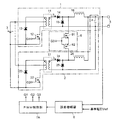
フォワード型DC/DCコンバータにおいて出力電力をさらに大きくするための手法の一つとして、インターリーブ方式によるフォワード型DC/DCコンバータが従来知られている。図4は特許文献1等に記載された従来のインターリーブ方式によるフォワード型DC/DCコンバータを用いたスイッチング電源装置の回路構成図、図5は該装置の動作を説明するための波形図、図6は該装置の電流経路を説明するための図である。
As a technique for further increasing the output power in the forward DC / DC converter, an interleaved forward DC / DC converter is conventionally known. FIG. 4 is a circuit configuration diagram of a switching power supply device using a conventional forward DC / DC converter described in
図4に示すように、このスイッチング電源装置において、図示しない負荷が接続される出力端5と直流電源3の間には、第1、第2なる二つのフォワード型DC/DCコンバータ1、2が並列に接続されている。この二つのフォワード型DC/DCコンバータ1、2は同一の回路構成を有する。即ち、第1フォワード型DC/DCコンバータ1において、トランス11の1次巻線の負極側端にはスイッチング素子(Nチャネル型FET)12のドレインが接続され、そのアノードは直流電源3の負極性端子に接続されている。また、トランス11の1次巻線の中間タップは直流電源3の正極性端子に接続され、該1次巻線の正極側端と直流電源3の負極性端子との間には電流阻止用のダイオード13が接続されている。一方、トランス11の2次巻線には、整流用ダイオード14、フライホイールダイオード15、及びリアクトル(インダクタ)16、及び平滑用コンデンサ4、を含む2次側回路が接続されている。
As shown in FIG. 4, in this switching power supply device, two forward DC /
第2のフォワード型DC/DCコンバータ2においても同様に、トランス21の1次巻線の負極側端にスイッチング素子(Nチャネル型FET)22のドレインが接続され、そのアノードは直流電源3の負極性端子に接続されている。また、トランス21の1次巻線の中間タップは直流電源3の正極性端子に接続され、該1次巻線の正極側端と直流電源3の負極性端子との間には電流阻止用のダイオード23が接続されている。一方、トランス21の2次巻線には、整流用ダイオード24、フライホイールダイオード25、及びリアクトル(インダクタ)26、及び平滑用コンデンサ4、を含む2次側回路が接続されている。
Similarly, in the second forward DC /
平滑用コンデンサ4は、第1、第2のフォワード型DC/DCコンバータ1、2で共用されている。また、フライホイールダイオード15のカソードとリアクトル16との接続点と、フライホイールダイオード25のカソードとリアクトル26との接続点との間は直結されている。したがって、二つのリアクトル16、26は実質的に並列に接続されており、等価的に一つのリアクトルであるとみなすことができる。
The smoothing capacitor 4 is shared by the first and second forward DC /
各フォワード型DC/DCコンバータ1、2の個々の動作は従来からよく知られており、例えば非特許文献1などに詳しく説明されている。
ここで、第2フォワード型DC/DCコンバータ2がないと仮定した場合の、第1フォワード型DC/DCコンバータ1のみにおける動作を簡単に説明する。
いま、スイッチング素子12がオンして直流電源3からトランス11の1次巻線に電流が供給されると、トランス11の2次巻線の両端にも電圧が発生し、整流用ダイオード14及びリアクトル16を通して出力端5に接続された負荷に電流(図4中のiL)が流れる。スイッチング素子12がターンオフされるとトランス11の2次巻線には電流は流れなくなるが、先にスイッチング素子12がオンしている期間にリアクトル16に蓄積された励磁エネルギーによって、該リアクトル16、負荷、フライホイールダイオード15を含む閉回路に電流が流れる。このようにスイッチング素子12のオン・オフ動作に関係なく同じ方向に流れる電流は平滑用コンデンサ4により平滑され、これによって、出力端5から負荷には同じ方向に(つまり直流の)電流iLが流れ続ける。
Individual operations of each of the forward type DC /
Here, the operation of only the first forward DC /
Now, when the
図4に示したインターリーブ方式によるフォワード型DC/DCコンバータでは、第1フォワード型DC/DCコンバータ1におけるスイッチング素子12をオン・オフ動作させる制御信号と、第2フォワード型DC/DCコンバータ2におけるスイッチング素子22をオン・オフ動作させる制御信号との位相を180°ずらすことにより、二つのフォワード型DC/DCコンバータ1、2を交互に動作させる。
In the forward DC / DC converter using the interleave method shown in FIG. 4, the control signal for turning on / off the
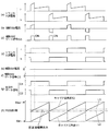
具体的に述べると、誤差増幅器6は出力端5に現れる電圧と基準電圧Vrefとの差(誤差)に応じた電圧をPWM制御部7Bに入力し、PWM制御部7Bは図5(e)に示すように、キャリア三角波信号と誤差増幅器6の出力電圧とのレベルを比較し、その比較結果に基づいて二つのスイッチング素子12、22をそれぞれオン・オフ動作させるPWM制御信号(図5(b)、(d)に示した主SWゲート信号)を生成する。したがって、PWM制御部7Bはキャリア三角波信号の1周期毎に、一方のスイッチング素子12をオン・オフ動作させる主SWゲート信号G1と他方のスイッチング素子22をオン・オフ動作させる主SWゲート信号G2とを交互に出力する。主SWゲート信号G1、G2は、キャリア三角波信号のスロープ開始点に同期して立ち上がり、そのスロープが誤差増幅器6の出力電圧を超える時点で立ち下がるパルス信号である。
More specifically, the
図5(b)は、図5(e)において誤差増幅器6の出力電圧がL1のレベルであるときの主SWゲート信号G1、G2である。また、図5(d)は、図5(e)において誤差増幅器6の出力電圧がL2のレベルであるときの主SWゲート信号G1、G2である。上述したように、トランス11、21の2次巻線にはスイッチング素子12、22がそれぞれオンしている期間にのみ電流i1、i2が流れる。そのため、それぞれの電流波形は図5(a)、(c)に示すようになる。
FIG. 5B shows the main SW gate signals G1 and G2 when the output voltage of the
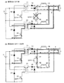
このフォワード型DC/DCコンバータでは、上述したように、二つのリアクトル16、26が並列に接続されている。そのため、図6(a)に示すように、第1のフォワード型DC/DCコンバータ1においてスイッチング素子12がオンしている期間にトランス11の2次巻線から整流用ダイオード14を通して流れる電流i1は、二つのリアクトル16、26に分岐してそれぞれ流れる。二つのリアクトル16、26の特性が揃っていれば、各リアクトル16、26にそれぞれ電流i1/2が流れる。そして、リアクトル16、26を通過したあとに両方の電流は合流し、平滑用コンデンサ4で平滑化されて出力端5から負荷に供給される。このとき、二つのリアクトル16、26にはいずれも励磁エネルギーが蓄積される。
In this forward type DC / DC converter, as described above, the two
スイッチング素子12がターンオフし、他方のスイッチング素子22がターンオンするまでの期間、つまり両方のスイッチング素子12がいずれもオフ状態であるときには、図6(b)に示すように、先に二つのリアクトル16、26にそれぞれ蓄積された励磁エネルギーによって、リアクトル16、負荷、フライホイールダイオード15を含む閉回路、及び、リアクトル26、負荷、フライホイールダイオード25を含む閉回路に電流が流れる。
In the period until the
第2フォワード型DC/DCコンバータ2においてスイッチング素子22がオンしている期間の動作は、上述した第1フォワード型DC/DCコンバータ1においてスイッチング素子12がオンしている期間の動作と基本的には同じである。このように、スイッチング素子12又は22のいずれかがオンしている期間にはトランス11又は21の2次巻線に発生した誘導電流が負荷に供給され、スイッチング素子12、22が共にオフしている期間にはリアクトル16、26に発生する起電力に由来する電流が負荷に供給される。したがって、平滑用コンデンサ4の手前で合流した電流i3は図5(f)に示すように、スイッチング素子12、22のオン・オフ動作に同期したものとなり、これが平滑化されてリップルが除去された電流iLが負荷に供給される。
The operation of the second forward type DC /
このスイッチング電源装置では、第1フォワード型DC/DCコンバータ1におけるトランス11及び整流用ダイオード14を通して出力される電力と、第2フォワード型DC/DCコンバータ2におけるトランス21及び整流用ダイオード24を通して出力される電力とを合計した電力を、リアクトル16、26及び平滑用コンデンサ4を介して出力端5から負荷に供給することができる。つまり、簡単に言えば、シングルタイプのフォワード型DC/DCコンバータの2倍の出力電力を負荷に供給することができる。また、このスイッチング電源装置では、最大出力電力の制約の下で、主SWゲート信号G1、G2のパルス幅を変える(つまり各信号のデューティ比を変える)ことによって出力端5から負荷に出力する電圧を調整することができる。
In this switching power supply device, the electric power output through the transformer 11 and the rectifying
特に産業用機器に使用されるスイッチング電源装置では、負荷の広範囲な変動に対応するために、最大定格電力内という制約の下で電圧出力及び電流出力をそれぞれ広範に変化させることが可能である特性が要求されることがある。例えば最大定格電力が2kWである場合に、最大出力電圧:400Vでは最大出力電流:5A、最大出力電圧:200Vでは最大出力電流:10Aというように、最大出力電圧を抑える一方、最大出力電流を増やす、又は逆に、最大出力電流を抑える一方、最大出力電圧を上げる、という柔軟な装置仕様が要求されることがある。こうした場合、スイッチング電源装置としての仕様の上での最大出力電力は2kWであるものの、上述した従来のインターリーブ方式によるフォワード型DC/DCコンバータを用いたスイッチング電源装置では、最大出力電圧と最大出力電流との積である4kW相当の電源容量の回路が必要となる。そのため、最大定格電力が同じ2kWで、最大出力電圧:400V、最大出力電流:5Aのみに対応可能であるスイッチング電源装置に比べると、各部品が高価であるために製品コストが増加するという問題がある。また、各部品が大きくなるために装置が大形になり重量も増すという問題もある。 Especially for switching power supplies used in industrial equipment, the characteristics of voltage output and current output can be varied widely under the restriction of within the maximum rated power in order to cope with a wide range of load fluctuations. May be required. For example, when the maximum rated power is 2 kW, the maximum output voltage is reduced to 5 A when the maximum output voltage is 400 V, and the maximum output current is 10 A when the maximum output voltage is 200 V, while the maximum output current is increased. Or, conversely, a flexible device specification that increases the maximum output voltage while suppressing the maximum output current may be required. In such a case, the maximum output power on the specifications as a switching power supply device is 2 kW, but in the switching power supply device using the above-described conventional interleaved forward type DC / DC converter, the maximum output voltage and the maximum output current. A circuit with a power capacity equivalent to 4kW, which is the product of Therefore, compared to a switching power supply device that can handle only the maximum rated power of 2 kW, the maximum output voltage: 400 V, and the maximum output current: 5 A, there is a problem that the product cost increases because each component is expensive. is there. Further, since each part becomes large, there is a problem that the apparatus becomes large and the weight increases.
本発明は上記課題を解決するためになされたものであり、その目的とするところは、トランス等の部品の小形化、低コスト化を図りながら、広範囲な負荷に対応可能であるスイッチング電源装置を提供することにある。 The present invention has been made to solve the above-mentioned problems, and an object of the present invention is to provide a switching power supply apparatus that can cope with a wide range of loads while reducing the size and cost of components such as a transformer. It is to provide.
上記課題を解決するためになされた本発明に係るスイッチング電源装置は、
a)トランスと、該トランスの1次巻線に直列に接続された主スイッチング部と、前記トランスの2次側回路に設けられたリアクトル及びフライホイールダイオードと、を含む第1のフォワード型DC/DCコンバータと、
b)前記第1のフォワード型DC/DCコンバータと同じ構成であり、その2次側回路の出力端が前記第1のフォワード型DC/DCコンバータの2次側回路の出力端と並列に接続されてなる第2のフォワード型DC/DCコンバータと、
c)前記第1のフォワード型DC/DCコンバータにおける2次側回路中のリアクトルの入力側と、前記第2のフォワード型DC/DCコンバータにおける2次側回路中のリアクトルの入力側と、の間に接続された補助スイッチング部と、
d)前記第1のフォワード型DC/DCコンバータにおける主スイッチング部、前記第2のフォワード型DC/DCコンバータにおける主スイッチング部、及び、前記補助スイッチング部のオン・オフ動作をそれぞれ制御する制御部と、
を備え、前記制御部は、前記補助スイッチング部をオフ状態に維持する一方、前記二つの主スイッチング部を交互にオン動作させる第1の動作モードと、前記二つの主スイッチング部を交互にオン動作させるとともに該主スイッチング部をそれぞれオン動作させている期間中の所定の期間、前記補助スイッチング部をオン動作させる第2の動作モードと、選択的に実行可能であることを特徴としている。
The switching power supply device according to the present invention made to solve the above problems is
a) a first forward type DC / DC including a transformer, a main switching unit connected in series to a primary winding of the transformer, and a reactor and a flywheel diode provided in a secondary side circuit of the transformer A DC converter;
b) The same configuration as that of the first forward type DC / DC converter, and the output end of the secondary side circuit thereof is connected in parallel with the output end of the secondary side circuit of the first forward type DC / DC converter. A second forward DC / DC converter,
c) Between the input side of the reactor in the secondary circuit in the first forward DC / DC converter and the input side of the reactor in the secondary circuit in the second forward DC / DC converter An auxiliary switching unit connected to
d) a control unit for controlling on / off operations of the main switching unit in the first forward DC / DC converter, the main switching unit in the second forward DC / DC converter, and the auxiliary switching unit; ,
The control unit maintains the auxiliary switching unit in an off state, while the two main switching units are alternately turned on, and the two main switching units are alternately turned on. And a second operation mode in which the auxiliary switching unit is turned on for a predetermined period of time during which the main switching unit is turned on, and is selectively executable.
通常、フォワード型DC/DCコンバータの2次側回路の最終段(リアクトルの後段)には平滑用コンデンサが接続されているが、本発明に係るスイッチング電源装置では、第1のフォワード型DC/DCコンバータと第2のフォワード型DC/DCコンバータとで平滑用コンデンサは共用してもよいし、或いはそれぞれ独立に平滑用コンデンサが設けられていてもよい。後者の場合、独立に設けられた二つの平滑用コンデンサは並列に接続されることになるから、実質的には一つのコンデンサであるとみなすことができる。 Normally, a smoothing capacitor is connected to the final stage of the secondary circuit of the forward type DC / DC converter (after the reactor). However, in the switching power supply according to the present invention, the first forward type DC / DC The smoothing capacitor may be shared by the converter and the second forward DC / DC converter, or a smoothing capacitor may be provided independently of each other. In the latter case, the two smoothing capacitors provided independently are connected in parallel, and thus can be regarded as one capacitor substantially.
また、一般にスイッチング電源装置は定電圧電源と定電流電源とに大別できるが、本発明に係るスイッチング電源装置はそのいずれにも対応可能である。定電圧電源とする場合には、本装置から負荷に出力される電圧が所望の電圧値になるように、制御部は各スイッチング部をオン・オフ動作させるパルス信号のパルス幅を調整すればよい。また、定電流電源とする場合には、本装置から負荷に供給される電流が所望の電流値になるように、制御部は各スイッチング部をオン・オフ動作させるパルス信号のパルス幅を調整すればよい。 In general, a switching power supply device can be broadly classified into a constant voltage power supply and a constant current power supply, but the switching power supply device according to the present invention can cope with both of them. In the case of a constant voltage power supply, the control unit may adjust the pulse width of the pulse signal for turning on / off each switching unit so that the voltage output from the device to the load has a desired voltage value. . In the case of a constant current power supply, the control unit adjusts the pulse width of the pulse signal for turning on / off each switching unit so that the current supplied from the device to the load has a desired current value. That's fine.
本発明に係るスイッチング電源装置において、第1の動作モードでは補助スイッチング部はオフ状態に維持されるから、これは補助スイッチング部が設けられていないのと同じである。一方、第2の動作モードにおいて補助スイッチング部がオン状態であるときには両リアクトルの入力側は実質的に直結されるから、これは上述した従来のインターリーブ方式によるフォワード型DC/DCコンバータを用いたスイッチング電源装置と同じ回路構成である。 In the switching power supply according to the present invention, the auxiliary switching unit is maintained in the off state in the first operation mode, which is the same as the case where the auxiliary switching unit is not provided. On the other hand, when the auxiliary switching unit is in the ON state in the second operation mode, the input sides of both reactors are substantially directly connected. This is a switching using the above-described conventional interleaved forward DC / DC converter. The circuit configuration is the same as that of the power supply device.
第1の動作モードにおいては、第1のフォワード型DC/DCコンバータにおける2次側回路中のリアクトルと、第2のフォワード型DC/DCコンバータにおける2次側回路中のリアクトルとは並列接続とならず、二つのフォワード型DC/DCコンバータは独立に動作する。つまり、これは、並列に接続されたシングルタイプのフォワード型DC/DCコンバータが、インターリーブ方式によって交互に駆動される状態である。そのため、一方のフォワード型DC/DCコンバータにおいてスイッチング素子がオン状態であり、そのトランスの2次巻線で誘起された電流がリアクトル、平滑用コンデンサを介して出力されているときに、他方のフォワード型DC/DCコンバータではそれ以前にリアクトルに蓄積された励磁エネルギーに由来する電流が出力される。その結果、二つのフォワード型DC/DCコンバータからそれぞれ出力される電流が加算され、本装置から出力可能な最大の電流は個々のフォワード型DC/DCコンバータの2倍になる。 In the first operation mode, the reactor in the secondary circuit in the first forward DC / DC converter and the reactor in the secondary circuit in the second forward DC / DC converter are connected in parallel. The two forward type DC / DC converters operate independently. That is, this is a state in which single-type forward DC / DC converters connected in parallel are alternately driven by an interleave method. Therefore, when the switching element is on in one forward type DC / DC converter and the current induced in the secondary winding of the transformer is output via the reactor and the smoothing capacitor, the other forward type DC / DC converter In the type DC / DC converter, a current derived from the excitation energy previously accumulated in the reactor is output. As a result, the currents output from the two forward DC / DC converters are added, and the maximum current that can be output from the present apparatus is twice that of the individual forward DC / DC converters.
ただし、第1のフォワード型DC/DCコンバータにおいてトランスを介して2次側回路へ供給される電力と、第2のフォワード型DC/DCコンバータにおいてトランスを介して2次側回路へ供給される電力との合計は、上述した従来のインターリーブ方式によるフォワード型DC/DCコンバータと同じであり、本発明に係るスイッチング装置からの出力電圧の最大値(最大出力電圧)はシングルタイプのフォワード型DC/DCコンバータによるスイッチング電源装置と同等である。即ち、本発明に係るスイッチング電源装置は、第1の動作モードで動作する際に、出力電圧の最大値はシングルタイプのフォワード型DC/DCコンバータによるスイッチング電源装置と同等であるが、出力電流の最大値はシングルタイプのフォワード型DC/DCコンバータによるスイッチング電源装置の2倍となり、出力電力も同様に2倍である。 However, the power supplied to the secondary circuit via the transformer in the first forward DC / DC converter and the power supplied to the secondary circuit via the transformer in the second forward DC / DC converter. Is the same as that of the above-described conventional interleaved forward DC / DC converter, and the maximum value (maximum output voltage) of the output voltage from the switching device according to the present invention is a single type forward DC / DC. It is equivalent to a switching power supply using a converter. That is, when the switching power supply according to the present invention operates in the first operation mode, the maximum value of the output voltage is equivalent to that of the switching power supply by the single type forward DC / DC converter, The maximum value is twice that of a switching power supply device using a single type forward DC / DC converter, and the output power is twice as well.
これに対し、第2の動作モードでは、制御部の制御の下で、例えば第1のフォワード型DC/DCコンバータにおける主スイッチング部がオン動作してトランスの2次巻線に誘導された電流が流れているときに、補助スイッチング部が所定期間、オン状態とされる。このオン状態である補助スイッチング部を介して、第1のフォワード型DC/DCコンバータにおけるトランスの2次巻線から流れる電流は第2のフォワード型DC/DCコンバータにおける2次側回路中のリアクトルにも分岐して流れる。そのため、補助スイッチング部がオン状態であるこの期間には、第2のフォワード型DC/DCコンバータにおいてリアクトルに蓄積されていた励磁エネルギーに由来する電流は流れず、逆に、該リアクトルに流れる電流によって励磁エネルギーが蓄積される。第2のフォワード型DC/DCコンバータにおける主スイッチング部がオン動作してトランスの2次巻線に誘導された電流が流れているときに、補助スイッチング部が所定期間、オン状態とされる場合も同様である。 On the other hand, in the second operation mode, under the control of the control unit, for example, the main switching unit in the first forward DC / DC converter is turned on, and the current induced in the secondary winding of the transformer is When flowing, the auxiliary switching unit is turned on for a predetermined period. The current flowing from the secondary winding of the transformer in the first forward type DC / DC converter passes through the auxiliary switching unit in the on state to the reactor in the secondary side circuit in the second forward type DC / DC converter. Also diverge and flow. Therefore, during this period in which the auxiliary switching unit is in the on state, the current derived from the excitation energy accumulated in the reactor in the second forward type DC / DC converter does not flow, but conversely, the current flowing in the reactor Excitation energy is accumulated. The auxiliary switching unit may be turned on for a predetermined period when the main switching unit in the second forward type DC / DC converter is turned on and the current induced in the secondary winding of the transformer flows. It is the same.
その結果、この第2の動作モードでは第1の動作モードに比べて、補助スイッチング部がオン状態になる期間に対応する分だけ、負荷に供給可能な電流は減少するものの、出力電圧を上げることができる。例えば、二つの主スイッチング部をそれぞれ最大のデューティ比(通常50%)でオン・オフ動作させ、補助スイッチング部を連続的にオン状態にしたときには、第1の動作モードにおいて二つの主スイッチング部をそれぞれ最大のデューティ比でオン・オフ動作させたときに比べて、最大出力電流は1/2になる代わりに、最大出力電圧は2倍になる。即ち、最大定格電力が2kW一定である場合に、第1の動作モードでは最大出力電圧:200V、最大出力電流:10Aの仕様を、また第2の動作モードでは最大出力電圧:400V、最大出力電流:5Aの仕様を実現することができる。 As a result, in the second operation mode, compared with the first operation mode, the current that can be supplied to the load is reduced by an amount corresponding to the period during which the auxiliary switching unit is turned on, but the output voltage is increased. Can do. For example, when two main switching units are turned on / off at the maximum duty ratio (usually 50%) and the auxiliary switching unit is continuously turned on, the two main switching units are switched on in the first operation mode. The maximum output current is doubled instead of halving the maximum output current as compared to when the on / off operation is performed at the maximum duty ratio. That is, when the maximum rated power is constant at 2 kW, the maximum output voltage is 200 V and the maximum output current is 10 A in the first operation mode, and the maximum output voltage is 400 V and the maximum output current in the second operation mode. : The specification of 5A can be realized.
上述した従来のインターリーブ方式によるフォワード型DC/DCコンバータを用いたスイッチング電源装置では、より広範囲な負荷に対応するために最大出力電流を増加させようとした場合、最大出力電力も増加させる必要があり、それに応じてトランス等の回路部品も大きくコストが高いものを使用する必要があった。それに対し、本発明に係るスイッチング電源装置によれば、最大定格電力が一定であれば、最大出力電圧と最大出力電流との組み合わせを変更した場合でも、各フォワード型DC−DCコンバータにおいてそれぞれ負担する電力は変わらない。そのため、トランス等の回路部品を大形化する必要がなく、装置の小形化、低コスト化を図りながら、広範囲な負荷に対応することができる。 In the switching power supply device using the above-described conventional interleaved forward type DC / DC converter, it is necessary to increase the maximum output power when attempting to increase the maximum output current in order to cope with a wider range of loads. Accordingly, it is necessary to use a circuit component such as a transformer which is large and expensive. On the other hand, according to the switching power supply device according to the present invention, if the maximum rated power is constant, even if the combination of the maximum output voltage and the maximum output current is changed, each forward DC-DC converter bears the load. Power does not change. Therefore, it is not necessary to increase the size of circuit components such as a transformer, and it is possible to cope with a wide range of loads while reducing the size and cost of the apparatus.
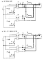
本発明の一実施例であるスイッチング電源装置について、添付図面を参照して説明する。図1は本実施例のスイッチング電源装置の回路構成図、図2は本実施例のスイッチング電源装置における動作を説明するための波形図、図3は本実施例のスイッチング電源装置における電流経路の説明図である。 A switching power supply device according to an embodiment of the present invention will be described with reference to the accompanying drawings. FIG. 1 is a circuit configuration diagram of the switching power supply device of the present embodiment, FIG. 2 is a waveform diagram for explaining the operation of the switching power supply device of the present embodiment, and FIG. 3 is an explanation of current paths in the switching power supply device of the present embodiment. FIG.
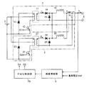
図1において、図4に示した従来のスイッチング電源装置と同じ構成要素には同じ符号を付している。本実施例のスイッチング電源装置では、第1フォワード型DC/DCコンバータ1におけるリアクトル16の入力側と第2フォワード型DC/DCコンバータ2におけるリアクトル26の入力側との間に、二つのNチャネル型FET81、82をソース端子、ドレイン端子を逆にして直列に接続した補助スイッチング回路8を設けている。そして、この二つのNチャネル型FET81、82のゲート端子には共通に、PWM制御部7Aから補助SWゲート信号G3が入力されている。PWM制御部7Aは、出力電圧と基準電圧Vrefとの差に応じた誤差電圧を誤差増幅器6から受ける点では従来のスイッチング電源装置におけるPWM制御部7Bと同じであるが、スイッチング素子12、22をオン・オフ動作させる主SWゲート信号G1、G2のほかに上記補助SWゲート信号G3を生成する点がPWM制御部7Bとは異なる。
1, the same components as those of the conventional switching power supply device shown in FIG. In the switching power supply of the present embodiment, two N-channel types are provided between the input side of the
図1から明らかであるように、本実施例のスイッチング電源装置において補助スイッチング回路8がオン状態であるときの回路構成は、図4に示した従来のスイッチング電源装置と同じである。
一方、補助スイッチング回路8がオフ状態であるときには、二つのリアクトル16、26の入力側同士は接続されないので、二つのフォワード型DC/DCコンバータ1、2の2次側回路は独立している(図1の回路では平滑用コンデンサ4は共用されているが、これはフォワード型DC/DCコンバータ1、2毎に設けられた平滑用コンデンサの並列接続であるとみることができる)。
As is apparent from FIG. 1, the circuit configuration when the
On the other hand, when the
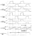
図2、図3を参照して、本実施例のスイッチング電源装置の動作を説明する。図2において(d)〜(g)は、低電圧・大電流動作モード(本発明における「第1の動作モード」に相当)における波形図の一例である。この低電圧・大電流動作モードでは、補助SWゲート信号G3はローレベルに維持され、補助スイッチング回路8はオフ状態のままであって、補助スイッチング回路8に電流が流れることもない(図2(e)、(f)参照)。図2(g)は、主SWゲート信号G1、G2がいずれもデューティ比が最大(50%)の場合の例であり、これは、誤差増幅器6からPWM制御部7Aに入力される誤差電圧が図2(h)のL2に示すレベルにあるときである。
With reference to FIG. 2 and FIG. 3, the operation of the switching power supply of the present embodiment will be described. 2, (d) to (g) are examples of waveform diagrams in the low voltage / high current operation mode (corresponding to the “first operation mode” in the present invention). In this low voltage / high current operation mode, the auxiliary SW gate signal G3 is maintained at a low level, the
例えば第1フォワード型DC/DCコンバータ1においてスイッチング素子12がオンしている期間には、トランス11の1次巻線に流れる電流によって2次巻線に誘導された電流i1が整流用ダイオード14、リアクトル16、平滑用コンデンサ4を介して負荷に流れる。この動作には第2フォワード型DC/DCコンバータ2におけるリアクトル26は全く関与しない。スイッチング素子12がターンオフしてトランス11の2次巻線に誘導される電流がなくなると、リアクトル16に蓄積されていた励磁エネルギーによる逆起電力によって、出力端5から負荷に先と同方向に電流が供給される(図3(a)中の太一点鎖線参照)。
For example, during the period when the switching
第2フォワード型DC/DCコンバータ2においてスイッチング素子22がターンオンしてトランス21の1次巻線に電流が流れると、今後はその2次巻線に誘導される電流i2がリアクトル26を経て出力端5から負荷に供給される(図3(a)中の太実線参照)。したがって、スイッチング素子22がオフ状態である期間には、第1フォワード型DC/DCコンバータ1からの電流と第2フォワード型DC/DCコンバータ2からの電流とが加算されて出力端5から負荷に供給される。つまり、この場合には、一つのフォワード型DC/DCコンバータから供給可能な電流の2倍の電流を負荷に供給することができる。このとき、二つのフォワード型DC/DCコンバータ1、2の動作はその位相がちょうど180°ずれているから、電流を加算する際にリップルが相殺され、低リップルの大電流を負荷に供給することができる。一方、出力電圧は一つのフォワード型DC/DCコンバータの出力電圧と同じである。
When the switching
例えば、一つのフォワード型DC/DCコンバータ1、2の最大定格電力が1kW、最大出力電圧が200V、最大出力電流が5Aであるとしたとき、この低電圧・大電流モードでは、最大定格電力が2kW、最大出力電圧が200V、最大出力電流が10Aの動作が可能である。そして、PWM制御部7Aから出力する主SWゲート信号G1、G2のパルス幅をデューティ比0〜50%の範囲で調整することによって、0〜200Vの範囲での定電圧出力を実現することができる。
For example, assuming that the maximum rated power of one forward type DC /
出力電圧を200V以上にする場合、動作モードは低電圧・大電流動作モードから高電圧・小電流動作モード(本発明における「第2の動作モード」に相当)に切り替わる。この高電圧・小電流動作モードでは、制御部7Aは主SWゲート信号G1、G2のデューティ比を共に最大(50%)に設定する。そして、PWM制御部7Aでは、誤差増幅器6から出力される誤差電圧のレベルをキャリア三角波信号T2と比較し、キャリア三角波信号T2のスロープ開始点に同期して立ち上がり、そのスロープが誤差電圧を超える時点で立ち下がるパルス信号を補助SWゲート信号G3として生成する。図2(c)は、図2(h)において誤差出力のレベルがL1であるときに生成される補助SWゲート信号G3の波形である。
When the output voltage is set to 200 V or more, the operation mode is switched from the low voltage / large current operation mode to the high voltage / small current operation mode (corresponding to the “second operation mode” in the present invention). In the high voltage / small current operation mode, the
補助SWゲート信号G3がローレベルである期間における各フォワード型DC/DCコンバータ1、2の動作は、上述した低電圧・大電流動作モードのときと同様である。一方、補助SWゲート信号G3がハイレベルになる期間には補助スイッチング回路8がオン状態となって、二つのリアクトル16、26の入力側が実質的に直結される。そのため、例えば第1フォワード型DC/DCコンバータ1におけるスイッチング素子12がオン状態であるときに補助スイッチング回路8がターンオンすると、リアクトル16を通してのみならず、補助スイッチング回路8を通して電流が第2フォワード型DC/DCコンバータ2側のリアクトル26にも流れる状態となり、トランス11の2次巻線に誘導される電流は一時的に増加する(図2(a)、(b)、図3(b)参照)。一方、それ以前にリアクトル26に蓄積されていた励磁エネルギーに由来する電流は流れなくなるため、その分、平滑用コンデンサ4を介して出力端5から負荷に供給され得る電流は減少する。つまり、最大出力電力は一定で、出力電圧が増加した分に見合うだけ出力電流は減少する。
The operations of the forward type DC /
そして、補助SWゲート信号SWのパルス幅を増加させていって最終的に常時補助スイッチング回路8がオンしている状態になると、図4に示した従来のインターリーブ方式によるフォワード型DC/DCコンバータを用いたスイッチング電源装置と同等であるから、最大出力電流は低電圧・大電流動作モードの1/2になる一方、最大出力電圧は2倍になる。即ち、一つのフォワード型DC/DCコンバータ1、2の最大定格電力が1kW、最大出力電圧が200V、最大出力電流が5Aであるとしたとき、この高電圧・小電流動作モードでは、最大定格電力が2kW、最大出力電圧が400V、最大出力電流が5Aの動作が可能である。そして、PWM制御部7Aから出力する補助SWゲート信号G3のパルス幅をデューティ比0〜100%の範囲で調整することによって、200〜400Vの範囲での定電圧出力を実現することができる。
Then, when the pulse width of the auxiliary SW gate signal SW is increased and finally the
本実施例のスイッチング電源装置では、低電圧大電流動作モード、高電圧・小電流動作モードのいずれでも、一つのフォワード型DC/DCコンバータ1、2の負担する電力は同じであり、回路の電力容量を増やす必要はない。そのため、上記動作モードに対応するために、トランス11、21等の回路部品を大容量対応のものに変更する必要はなく、装置の小形化、低コスト化を図りながら、広範囲な負荷への対応が可能となる。
In the switching power supply device of the present embodiment, the power borne by one forward type DC /
なお、上記実施例は本発明の一例にすぎず、本発明の趣旨の範囲で適宜変形、修正、追加を行っても本願特許請求の範囲に包含されることは当然である。 It should be noted that the above embodiment is merely an example of the present invention, and it will be understood that the present invention is encompassed in the scope of the claims of the present application even if appropriate modifications, corrections and additions are made within the scope of the present invention.
1、2…フォワード型DC/DCコンバータ
11、21…トランス
12、22…スイッチング素子
13、23…ダイオード
14、24…整流用ダイオード
15、25…フライホイールダイオード
16、26…リアクトル
3…直流電源
4…平滑用コンデンサ
5…出力端
6…誤差増幅器
7A…PWM制御部
8…補助スイッチング回路
81、82…Nチャネル型FET
DESCRIPTION OF
Claims (2)
b)前記第1のフォワード型DC/DCコンバータと同じ構成であり、その2次側回路の出力端が前記第1のフォワード型DC/DCコンバータの2次側回路の出力端と並列に接続されてなる第2のフォワード型DC/DCコンバータと、
c)前記第1のフォワード型DC/DCコンバータにおける2次側回路中のリアクトルの入力側と、前記第2のフォワード型DC/DCコンバータにおける2次側回路中のリアクトルの入力側と、の間に接続された補助スイッチング部と、
d)前記第1のフォワード型DC/DCコンバータにおける主スイッチング部、前記第2のフォワード型DC/DCコンバータにおける主スイッチング部、及び、前記補助スイッチング部のオン・オフ動作をそれぞれ制御する制御部と、
を備え、前記制御部は、前記補助スイッチング部をオフ状態に維持する一方、前記二つの主スイッチング部を交互にオン動作させる第1の動作モードと、前記二つの主スイッチング部を交互にオン動作させるとともに該主スイッチング部をそれぞれオン動作させている期間中の所定の期間、前記補助スイッチング部をオン動作させる第2の動作モードと、選択的に実行可能であることを特徴とするスイッチング電源装置。 a) a first forward type DC / DC including a transformer, a main switching unit connected in series to a primary winding of the transformer, and a reactor and a flywheel diode provided in a secondary side circuit of the transformer A DC converter;
b) The same configuration as that of the first forward type DC / DC converter, and the output end of the secondary side circuit thereof is connected in parallel with the output end of the secondary side circuit of the first forward type DC / DC converter. A second forward DC / DC converter,
c) Between the input side of the reactor in the secondary circuit in the first forward DC / DC converter and the input side of the reactor in the secondary circuit in the second forward DC / DC converter An auxiliary switching unit connected to
d) a control unit for controlling on / off operations of the main switching unit in the first forward DC / DC converter, the main switching unit in the second forward DC / DC converter, and the auxiliary switching unit; ,
The control unit maintains the auxiliary switching unit in an off state, while the two main switching units are alternately turned on, and the two main switching units are alternately turned on. And a second operation mode in which the auxiliary switching unit is turned on for a predetermined period of time during which each of the main switching units is turned on, and a switching power supply device that is selectively executable .
前記制御部は、当該装置から負荷に出力される電圧が所望の電圧値になるように、前記二つの主スイッチング部及び前記補助スイッチング部をオン・オフ動作させるパルス信号のパルス幅を調整することを特徴とするスイッチング電源装置。 The switching power supply device according to claim 1,
The control unit adjusts a pulse width of a pulse signal for turning on and off the two main switching units and the auxiliary switching unit so that a voltage output from the device to a load has a desired voltage value. A switching power supply device.
Priority Applications (1)
| Application Number | Priority Date | Filing Date | Title |
|---|---|---|---|
| JP2015090162A JP6417543B2 (en) | 2015-04-27 | 2015-04-27 | Switching power supply |
Applications Claiming Priority (1)
| Application Number | Priority Date | Filing Date | Title |
|---|---|---|---|
| JP2015090162A JP6417543B2 (en) | 2015-04-27 | 2015-04-27 | Switching power supply |
Publications (2)
| Publication Number | Publication Date |
|---|---|
| JP2016208756A JP2016208756A (en) | 2016-12-08 |
| JP6417543B2 true JP6417543B2 (en) | 2018-11-07 |
Family
ID=57490869
Family Applications (1)
| Application Number | Title | Priority Date | Filing Date |
|---|---|---|---|
| JP2015090162A Expired - Fee Related JP6417543B2 (en) | 2015-04-27 | 2015-04-27 | Switching power supply |
Country Status (1)
| Country | Link |
|---|---|
| JP (1) | JP6417543B2 (en) |
Family Cites Families (5)
| Publication number | Priority date | Publication date | Assignee | Title |
|---|---|---|---|---|
| JPH03150068A (en) * | 1989-11-06 | 1991-06-26 | Sansha Electric Mfg Co Ltd | Switching power source circuit |
| JPH08103073A (en) * | 1994-09-30 | 1996-04-16 | Terekomu Kiki Kk | Switching power supply equipment |
| JP5061368B2 (en) * | 2008-01-28 | 2012-10-31 | エヌイーシーコンピュータテクノ株式会社 | Power supply circuit |
| JP5243295B2 (en) * | 2009-02-18 | 2013-07-24 | オリジン電気株式会社 | Power circuit |
| JP2011205752A (en) * | 2010-03-25 | 2011-10-13 | Fujitsu Telecom Networks Ltd | Forward-type switching power supply device and drive method of forward-type switching power supply device |
-
2015
- 2015-04-27 JP JP2015090162A patent/JP6417543B2/en not_active Expired - Fee Related
Also Published As
| Publication number | Publication date |
|---|---|
| JP2016208756A (en) | 2016-12-08 |
Similar Documents
| Publication | Publication Date | Title |
|---|---|---|
| JP5929703B2 (en) | DC / DC converter | |
| CN110663165B (en) | DC/DC converter | |
| US20110069514A1 (en) | Dc conversion apparatus | |
| US8780585B2 (en) | Double phase-shifting full-bridge DC-to-DC converter | |
| JP6752335B2 (en) | DC / DC converter | |
| WO2016031061A1 (en) | Power factor improving converter and power supply device including power factor improving converter | |
| JP2014204660A (en) | Integrated converter with single-ended control, power factor correction, and low output ripple | |
| WO2018116437A1 (en) | Power conversion device | |
| JP6012822B1 (en) | Power converter | |
| JP4715429B2 (en) | AC / DC converter | |
| US11329566B2 (en) | DC power supply circuit that enhances stability of output voltage | |
| JP2014239579A (en) | Dc/dc converter and battery charging/discharging device | |
| WO2017149906A1 (en) | Switching power supply circuit | |
| JP2016086562A (en) | Power circuit | |
| JP2019097273A (en) | Power conversion device | |
| JP6417543B2 (en) | Switching power supply | |
| JP2017017845A (en) | High voltage generator | |
| JP2017017868A (en) | DC-AC conversion circuit and power supply device | |
| JP2014014232A (en) | Dc power supply device | |
| JP4684758B2 (en) | Power supply | |
| JP2008245388A (en) | Switching power supply | |
| JP2003289665A (en) | Switching power supply unit | |
| CN109075716B (en) | Clocked power supply unit with electrical isolation | |
| JP2024029561A (en) | power converter | |
| JP6557035B2 (en) | Switching power supply circuit and switching power supply control method |
Legal Events
| Date | Code | Title | Description |
|---|---|---|---|
| A621 | Written request for application examination |
Free format text: JAPANESE INTERMEDIATE CODE: A621 Effective date: 20170509 |
|
| A131 | Notification of reasons for refusal |
Free format text: JAPANESE INTERMEDIATE CODE: A131 Effective date: 20180109 |
|
| A601 | Written request for extension of time |
Free format text: JAPANESE INTERMEDIATE CODE: A601 Effective date: 20180312 |
|
| TRDD | Decision of grant or rejection written | ||
| A01 | Written decision to grant a patent or to grant a registration (utility model) |
Free format text: JAPANESE INTERMEDIATE CODE: A01 Effective date: 20180828 |
|
| A61 | First payment of annual fees (during grant procedure) |
Free format text: JAPANESE INTERMEDIATE CODE: A61 Effective date: 20180910 |
|
| R150 | Certificate of patent or registration of utility model |
Ref document number: 6417543 Country of ref document: JP Free format text: JAPANESE INTERMEDIATE CODE: R150 |
|
| R250 | Receipt of annual fees |
Free format text: JAPANESE INTERMEDIATE CODE: R250 |
|
| LAPS | Cancellation because of no payment of annual fees |