JP6388595B2 - Color conversion device, lighting unit, solid state light emitter package, and lighting fixture - Google Patents
Color conversion device, lighting unit, solid state light emitter package, and lighting fixture Download PDFInfo
- Publication number
- JP6388595B2 JP6388595B2 JP2015546126A JP2015546126A JP6388595B2 JP 6388595 B2 JP6388595 B2 JP 6388595B2 JP 2015546126 A JP2015546126 A JP 2015546126A JP 2015546126 A JP2015546126 A JP 2015546126A JP 6388595 B2 JP6388595 B2 JP 6388595B2
- Authority
- JP
- Japan
- Prior art keywords
- layer
- luminescent
- light
- conversion device
- color conversion
- Prior art date
- Legal status (The legal status is an assumption and is not a legal conclusion. Google has not performed a legal analysis and makes no representation as to the accuracy of the status listed.)
- Expired - Fee Related
Links
Images


Classifications
-
- H—ELECTRICITY
- H01—ELECTRIC ELEMENTS
- H01L—SEMICONDUCTOR DEVICES NOT COVERED BY CLASS H10
- H01L33/00—Semiconductor devices with at least one potential-jump barrier or surface barrier specially adapted for light emission; Processes or apparatus specially adapted for the manufacture or treatment thereof or of parts thereof; Details thereof
- H01L33/48—Semiconductor devices with at least one potential-jump barrier or surface barrier specially adapted for light emission; Processes or apparatus specially adapted for the manufacture or treatment thereof or of parts thereof; Details thereof characterised by the semiconductor body packages
- H01L33/64—Heat extraction or cooling elements
- H01L33/641—Heat extraction or cooling elements characterized by the materials
-
- F—MECHANICAL ENGINEERING; LIGHTING; HEATING; WEAPONS; BLASTING
- F21—LIGHTING
- F21V—FUNCTIONAL FEATURES OR DETAILS OF LIGHTING DEVICES OR SYSTEMS THEREOF; STRUCTURAL COMBINATIONS OF LIGHTING DEVICES WITH OTHER ARTICLES, NOT OTHERWISE PROVIDED FOR
- F21V29/00—Protecting lighting devices from thermal damage; Cooling or heating arrangements specially adapted for lighting devices or systems
- F21V29/50—Cooling arrangements
- F21V29/70—Cooling arrangements characterised by passive heat-dissipating elements, e.g. heat-sinks
-
- F—MECHANICAL ENGINEERING; LIGHTING; HEATING; WEAPONS; BLASTING
- F21—LIGHTING
- F21V—FUNCTIONAL FEATURES OR DETAILS OF LIGHTING DEVICES OR SYSTEMS THEREOF; STRUCTURAL COMBINATIONS OF LIGHTING DEVICES WITH OTHER ARTICLES, NOT OTHERWISE PROVIDED FOR
- F21V9/00—Elements for modifying spectral properties, polarisation or intensity of the light emitted, e.g. filters
- F21V9/30—Elements containing photoluminescent material distinct from or spaced from the light source
- F21V9/38—Combination of two or more photoluminescent elements of different materials
-
- H—ELECTRICITY
- H01—ELECTRIC ELEMENTS
- H01L—SEMICONDUCTOR DEVICES NOT COVERED BY CLASS H10
- H01L33/00—Semiconductor devices with at least one potential-jump barrier or surface barrier specially adapted for light emission; Processes or apparatus specially adapted for the manufacture or treatment thereof or of parts thereof; Details thereof
- H01L33/48—Semiconductor devices with at least one potential-jump barrier or surface barrier specially adapted for light emission; Processes or apparatus specially adapted for the manufacture or treatment thereof or of parts thereof; Details thereof characterised by the semiconductor body packages
- H01L33/50—Wavelength conversion elements
- H01L33/501—Wavelength conversion elements characterised by the materials, e.g. binder
- H01L33/502—Wavelength conversion materials
-
- H—ELECTRICITY
- H01—ELECTRIC ELEMENTS
- H01L—SEMICONDUCTOR DEVICES NOT COVERED BY CLASS H10
- H01L33/00—Semiconductor devices with at least one potential-jump barrier or surface barrier specially adapted for light emission; Processes or apparatus specially adapted for the manufacture or treatment thereof or of parts thereof; Details thereof
- H01L33/48—Semiconductor devices with at least one potential-jump barrier or surface barrier specially adapted for light emission; Processes or apparatus specially adapted for the manufacture or treatment thereof or of parts thereof; Details thereof characterised by the semiconductor body packages
- H01L33/64—Heat extraction or cooling elements
- H01L33/644—Heat extraction or cooling elements in intimate contact or integrated with parts of the device other than the semiconductor body
-
- H—ELECTRICITY
- H01—ELECTRIC ELEMENTS
- H01L—SEMICONDUCTOR DEVICES NOT COVERED BY CLASS H10
- H01L2924/00—Indexing scheme for arrangements or methods for connecting or disconnecting semiconductor or solid-state bodies as covered by H01L24/00
- H01L2924/0001—Technical content checked by a classifier
- H01L2924/0002—Not covered by any one of groups H01L24/00, H01L24/00 and H01L2224/00
Description
本発明は、第1の色の光を第2の色の光へと変換するルミネッセント材料を含む色変換装置に関する。本発明は、更に、照明ユニット、固体発光体パッケージ、照明器具、及びグラフェン層の使用に関する。 The present invention relates to a color conversion device that includes a luminescent material that converts light of a first color into light of a second color. The invention further relates to the use of lighting units, solid state light emitter packages, lighting fixtures and graphene layers.
ルミネッセント材料において、第1のスペクトル分布の光が吸収され、部分的に第2のスペクトル分布の光へと変換される。全ての吸収されたエネルギーが光の形で放射される訳ではない。一部のエネルギーは、ルミネッセント材料のストークスシフトにより、熱へと変換される。ストークスシフトは、吸収スペクトル分布の位置と、発光スペクトル分布の位置との差である。吸収された光子は、より低量のエネルギーを有した光子として放射され、放射されないエネルギーは、熱へと転換される。 In the luminescent material, light of the first spectral distribution is absorbed and partially converted to light of the second spectral distribution. Not all absorbed energy is emitted in the form of light. Some energy is converted to heat by the Stokes shift of the luminescent material. The Stokes shift is the difference between the position of the absorption spectrum distribution and the position of the emission spectrum distribution. Absorbed photons are emitted as photons with lower amounts of energy, and unemitted energy is converted to heat.
ルミネッセント材料の温度が高くなり過ぎると、ルミネッセント材料の作用は、悪影響を受け、場合によっては、ルミネッセント材料が劣化し得る又は破壊され得る。ルミネッセント材料が温かくなり過ぎると、ルミネッセント材料の劣化及び/又は破壊により、それらの変換効率が大幅に低下し、それらの発光スペクトルが変化し得る、及びそれらの寿命が減少される。更に、ルミネッセント材料が熱くなる場合、ルミネッセント材料が分散された若しくは溶解された材料、又はルミネッセント材料が上に設けられた材料もまた、耐熱性でなければならず、劣化及び/又は破壊を受け得る。 If the temperature of the luminescent material becomes too high, the action of the luminescent material will be adversely affected and in some cases the luminescent material may be degraded or destroyed. If the luminescent materials become too warm, degradation and / or destruction of the luminescent materials will greatly reduce their conversion efficiency, their emission spectra may change, and their lifetime will be reduced. Furthermore, if the luminescent material becomes hot, the material in which the luminescent material is dispersed or dissolved, or the material on which the luminescent material is provided must also be heat resistant and can be subject to degradation and / or destruction. .
ルミネッセント材料は、層状に施される事が多く、層に衝突した光は、層全体に亘って均一に広がらない事が多い。従って、多くの場合、ルミネッセント材料を有した層において、温度勾配が存在する。温度勾配は、温度勾配を受ける材料において、応力の生成という追加の欠点を有する。 Luminescent materials are often applied in layers, and light that strikes a layer often does not spread uniformly throughout the layer. Therefore, in many cases there is a temperature gradient in the layer with the luminescent material. Temperature gradients have the additional disadvantage of generating stress in materials that are subject to temperature gradients.
公開された特許出願である国際公開第2010/002708A1号は、第1の色から別の色の光へと光を変換する蛍光体層を含む発光デバイスに関する。蛍光体層は、凹部ハウジング上に設けられ、凹部は、第1の色の光を蛍光体層へと放射する発光半導体を含む。蛍光体層の一部のみが第1の色の光で照明され、ストークスシフトの結果、蛍光体層のこの部分は、比較的熱くなる。蛍光体層は、透明層と接触していてもよく、蛍光体層及び透明層の組み合わせは、発光デバイスの動作中、局所的に比較的熱くなる。前述の特許出願においては、凹部ハウジングは、蛍光体層及び/又は透明層から出るように熱を伝導可能な熱伝導性材料から作られる。 Published patent application WO 2010/002708 A1 relates to a light emitting device including a phosphor layer that converts light from a first color to another color of light. The phosphor layer is provided on the recess housing, and the recess includes a light emitting semiconductor that emits light of the first color to the phosphor layer. Only a portion of the phosphor layer is illuminated with the first color light, and as a result of the Stokes shift, this portion of the phosphor layer becomes relatively hot. The phosphor layer may be in contact with the transparent layer, and the combination of the phosphor layer and the transparent layer becomes locally relatively hot during operation of the light emitting device. In the aforementioned patent application, the recessed housing is made from a thermally conductive material capable of conducting heat away from the phosphor layer and / or the transparent layer.
前述の特許出願の発光デバイスは、蛍光体層を冷却する手段を設けるが、それでもなお、蛍光体層及び/又は蛍光体層が接触する透明層内において、大き過ぎる温度勾配が動作中に存在する。例えば、透明層は、蛍光体層内部の温度差を減少させるべきであるが、蛍光体層から透明層への熱伝達が効率的ではない及び透明層自体がハウジングへと十分な熱を伝導しない。 The light emitting devices of the aforementioned patent applications provide a means for cooling the phosphor layer, but nevertheless there is an excessively large temperature gradient during operation in the phosphor layer and / or the transparent layer with which the phosphor layer contacts. . For example, the transparent layer should reduce the temperature difference inside the phosphor layer, but the heat transfer from the phosphor layer to the transparent layer is not efficient and the transparent layer itself does not conduct enough heat to the housing .
本発明の目的は、色変換装置内の温度差を低減する色変換装置を提供する事である。 An object of the present invention is to provide a color conversion device that reduces a temperature difference in the color conversion device.
本発明の第1の態様は、色変換装置を提供する。本発明の第2の態様は、照明ユニットを提供する。本発明の第3の態様は、固体発光体パッケージを提供する。本発明の第4の態様は、照明器具を提供する。本発明の第5の態様は、グラフェン層の使用に関する。有利な実施形態は、従属クレームに定義される。 A first aspect of the present invention provides a color conversion apparatus. A second aspect of the present invention provides a lighting unit. A third aspect of the present invention provides a solid state light emitter package. A fourth aspect of the present invention provides a lighting fixture. A fifth aspect of the invention relates to the use of a graphene layer. Advantageous embodiments are defined in the dependent claims.
本発明の第1の態様による色変換装置は、第1のルミネッセント層、支持層及び第1のグラフェン層を含む。色変換装置は、第1の色の光を別の色の光に変換する為のものである。第1のルミネッセント層は、第1の色を含む第1のスペクトル分布の光の一部を吸収し、吸収された光の少なくとも一部を第2のスペクトル分布の光へと変換する第1のルミネッセント材料を含む。支持層は、ルミネッセント層を支持する。第1のグラフェン層は、色変換装置内の温度差が低減されるように、熱を横方向に熱伝導する。第1の任意選択の層構成では、支持層は固体発光体の層によって形成される、並びにルミネッセント層及びグラフェン層のスタックは、固体発光体の層上に設けられる。固体発光体の層の発光面は、ルミネッセント層又はグラフェン層と接触する。第2の任意選択の層構成では、支持層は、第1の面及び第1の面とは反対側の第2の面を含み、第1のグラフェン層は、支持層の第1の面に設けられ、並びにルミネッセント層は、第2の面に設けられる。グラフェン層は、支持層に熱的に結合される、及び第1のルミネッセント層は、支持層に熱的に結合される。第3の任意選択の層構成では、色変換装置は第2のグラフェン層を含む、及び第1のルミネッセント層は、第1のグラフェン層と第2のグラフェン層との間に挟持される。グラフェン層及び第1のルミネッセント層のスタックは、支持層上に設けられる。第4の任意選択の層構成では、色変換装置は、第2のルミネッセント材料を含む第2のルミネッセント層を含む。第1のグラフェン層は、第1のルミネッセント層と第2のルミネッセント層との間に挟持される、並びにルミネッセント層及び第1のグラフェン層のスタックは、支持層上に設けられる。第2のルミネッセント材料は、第1の色を含む第3のスペクトル分布の光及び/又は第2のスペクトル分布の光の一部を吸収し、吸収された光の少なくとも一部を第4のスペクトル分布の光へと変換する。 The color conversion device according to the first aspect of the present invention includes a first luminescent layer, a support layer, and a first graphene layer. The color conversion device is for converting light of a first color into light of another color. The first luminescent layer absorbs a portion of the light having the first spectral distribution including the first color and converts at least a portion of the absorbed light into light having the second spectral distribution. Contains luminescent material. The support layer supports the luminescent layer. The first graphene layer conducts heat laterally so that a temperature difference in the color conversion device is reduced. In a first optional layer configuration, the support layer is formed by a layer of solid state light emitter, and a stack of luminescent and graphene layers is provided on the layer of solid state light emitter. The light emitting surface of the solid phosphor layer is in contact with the luminescent layer or the graphene layer. In a second optional layer configuration, the support layer includes a first surface and a second surface opposite the first surface, and the first graphene layer is on the first surface of the support layer. A luminescent layer is provided on the second surface. The graphene layer is thermally coupled to the support layer, and the first luminescent layer is thermally coupled to the support layer. In a third optional layer configuration, the color conversion device includes a second graphene layer, and the first luminescent layer is sandwiched between the first graphene layer and the second graphene layer. A stack of graphene layers and a first luminescent layer is provided on the support layer. In a fourth optional layer configuration, the color conversion device includes a second luminescent layer that includes a second luminescent material. The first graphene layer is sandwiched between the first luminescent layer and the second luminescent layer, and the stack of the luminescent layer and the first graphene layer is provided on the support layer. The second luminescent material absorbs light of the third spectral distribution including the first color and / or part of the light of the second spectral distribution, and at least part of the absorbed light is the fourth spectrum. Convert to light of distribution.
色変換装置では、少なくとも1つのグラフェン層は、第1のルミネッセント層と直接接触する、又は1つのグラフェン層は、支持層を介してそれが第1のルミネッセント層と熱的に結合される特定の位置に設けられる。従って、グラフェン層は、第1のルミネッセント層で生成された熱を受ける。グラフェンは、非常に良く熱を伝導する事ができ、その結果、少なくとも1つのグラフェン層は、色変換装置の比較的温かい部分から色変換装置の比較的冷たい部分へと熱を伝導し、それによって、全体として色変換装置内の温度差を低減する。従って、ルミネッセント層のピーク温度が低下する、及び色変換装置の他の領域が許容限界内でより暖かくなる。その結果、熱過ぎるルミネッセント材料の悪影響が低減され、従って、ルミネッセント材料は、より長い寿命を持ち、比較的高い変換効率を持ち、劣化を受ける事が少なくなり、発光スペクトルの変化が低減されるであろう。更に、支持層の温度は、第1のグラフェン層を持たない色変換装置の場合ほど高くはならず、支持層における温度勾配は、より低い温度差を示すであろう。従って、支持層は、これらの大きな温度差に耐える必要はなく、任意選択的に、より費用のかからない材料から製造されてもよい。 In the color conversion device, at least one graphene layer is in direct contact with the first luminescent layer, or one graphene layer is a specific layer in which it is thermally coupled to the first luminescent layer via a support layer. Provided in position. Thus, the graphene layer receives the heat generated by the first luminescent layer. Graphene can conduct heat very well, so that at least one graphene layer conducts heat from a relatively warm part of the color conversion device to a relatively cool part of the color conversion device, thereby As a whole, the temperature difference in the color conversion device is reduced. Thus, the peak temperature of the luminescent layer is reduced and other areas of the color conversion device are warmer within acceptable limits. As a result, the negative effects of luminescent materials that are too hot are reduced, and therefore luminescent materials have a longer lifetime, have a relatively high conversion efficiency, are less susceptible to degradation, and reduce changes in the emission spectrum. I will. Furthermore, the temperature of the support layer will not be as high as in the case of a color conversion device without the first graphene layer, and the temperature gradient in the support layer will show a lower temperature difference. Thus, the support layer need not withstand these large temperature differences and may optionally be made from a less expensive material.
グラフェンは、原子スケールハニカム格子の炭素原子の単層を含む又はそのような原子スケールハニカム格子の炭素原子の単層を2〜9含む材料である。ハニカム格子の炭素原子が9層を超えると、材料の特徴が大幅に変化し、その材料は、「グラファイト」と呼ばれる。本発明の状況では、グラフェンが熱伝導性である及び光透過性である(これは、材料に衝突する光のかなりの部分が材料を透過する事を意味する)であるかどうかが関係あり、従って、グラフェンは、原子スケールハニカム格子の1〜9の炭素原子層を有し得る。単層グラフェンは、可視光の約2.3%を吸収する。ある実施形態では、グラフェン層は、原子スケールハニカム格子の5未満の炭素原子層を有する。 Graphene is a material that includes a single layer of carbon atoms in an atomic scale honeycomb lattice or 2-9 of a single layer of carbon atoms in such an atomic scale honeycomb lattice. When the number of carbon atoms in the honeycomb lattice exceeds nine layers, the material characteristics change drastically and the material is called “graphite”. In the context of the present invention, it is relevant whether the graphene is thermally conductive and light transmissive (which means that a significant portion of the light impinging on the material is transmitted through the material), Thus, the graphene can have 1-9 carbon atom layers of an atomic scale honeycomb lattice. Single layer graphene absorbs about 2.3% of visible light. In some embodiments, the graphene layer has less than 5 carbon atom layers in an atomic scale honeycomb lattice.
支持層は、色変換装置中の別個の層でもよいが、別のデバイスの層でもよい。支持層の機能は、少なくとも第1のルミネッセント層(これは、特定の実施形態では、それ自体の重さを支える事ができない)及び/又は第2のルミネッセント層を支持する事、並びに場合によっては第1及び/又は第2のグラフェン層を支持する事である。特定の実施形態では、支持層は、基板層又は固体発光体(例えば発光ダイオード等)の別の層(例えば、固体発光体のダイ)であり、そのような特定の実施形態では、グラフェン層は、固体発光体及び色変換装置を含む発光体パッケージ内の温度差も低減する。実用的実施形態では、支持層は、光透過性である。別の実用的実施形態では、支持層は、例えば0.1W/(m・K)を超える、又は別の任意選択的実施形態では1W/(m・K)を超える比較的低い熱伝導率を有する。 The support layer may be a separate layer in the color conversion device, but may also be a layer of another device. The function of the support layer is to support at least the first luminescent layer (which in certain embodiments cannot support its own weight) and / or the second luminescent layer, and possibly Supporting the first and / or second graphene layers. In certain embodiments, the support layer is a substrate layer or another layer of a solid light emitter (eg, a light emitting diode) (eg, a solid light emitter die), and in such specific embodiments, the graphene layer is Also, the temperature difference in the light emitter package including the solid light emitter and the color conversion device is reduced. In practical embodiments, the support layer is light transmissive. In another practical embodiment, the support layer has a relatively low thermal conductivity, for example greater than 0.1 W / (m · K), or in another optional embodiment greater than 1 W / (m · K). Have.
上記のセクション及び本出願において、「光透過性」という用語は、光が光透過材料を透過可能である事を示す為に使用される。従って、光が材料に衝突した場合、少なくとも一部の光は、材料を透過する(従って、材料の特定の表面で材料を離れる)。全ての光が材料を透過する必要はなく、一部の光は、吸収され得る(例えば、衝突した光の10%未満若しくは衝突した光の3%未満)及び/又は一部の衝突した光は反射され得る(例えば、衝突した光の25%未満若しくは衝突した光の10%未満)。光は、光透過材料内で散乱され得る。光透過性という用語は、「透明」及び「半透明」という用語を含む。 In the above section and in this application, the term “light transmissive” is used to indicate that light can be transmitted through a light transmissive material. Thus, when light strikes a material, at least some light is transmitted through the material (thus leaving the material at a particular surface of the material). Not all light needs to pass through the material, some light can be absorbed (eg, less than 10% of collided light or less than 3% of collided light) and / or some collided light is It can be reflected (eg, less than 25% of the impinged light or less than 10% of the impinged light). Light can be scattered within the light transmissive material. The term light transmissive includes the terms “transparent” and “translucent”.
上記のセクション及び本出願において、「熱的に結合される」という用語は、第1の材料が第2の材料と直接的又は間接的熱伝達経路を有する事を示す為に使用される。つまり、熱の形態のエネルギーは、第1の材料から第2の材料へ及びその逆に伝達される事が可能である。第1の材料は、第2の材料と直接接触してもよいが、他の材料をそれらが断熱材でない限り第1の材料と第2の材料との間に設けてもよい。例えば、第1及び第2の材料が互いに直接接触する場合は熱伝導経路を第1の材料と第2の材料との間に設けてもよい、又は比較的薄い接着層を用いて第1の材料を第2の材料に接着させてもよい。更に、本出願において、2つの層が互いに重なりあって設けられる及び/又は互いに直接接触する場合、それは、これら2つの層が熱的に互いに結合されている事も暗に開示している。 In the above section and in this application, the term “thermally coupled” is used to indicate that the first material has a direct or indirect heat transfer path with the second material. That is, energy in the form of heat can be transferred from the first material to the second material and vice versa. The first material may be in direct contact with the second material, but other materials may be provided between the first material and the second material as long as they are not thermal insulation. For example, if the first and second materials are in direct contact with each other, a heat conduction path may be provided between the first material and the second material, or the first and second materials may be used with a relatively thin adhesive layer. The material may be adhered to the second material. Furthermore, in the present application, where two layers are provided overlapping each other and / or in direct contact with each other, it also implicitly discloses that these two layers are thermally bonded to each other.
第2のルミネッセント材料は、第1の色を含む第3のスペクトル分布の光を吸収するように構成されてもよい。これは、第3のスペクトル分布が第1のスペクトル分布と一部重複してもよい事を意味する。ある実施形態では、第3のスペクトル分布は、第1のスペクトル分布と実質的に等しい。 The second luminescent material may be configured to absorb light of a third spectral distribution that includes the first color. This means that the third spectral distribution may partially overlap with the first spectral distribution. In certain embodiments, the third spectral distribution is substantially equal to the first spectral distribution.
任意選択的に、色変換装置は、ヒートシンクに熱的に結合される熱伝達インタフェースを含み、第1のグラフェン層及び任意選択的に任意選択の第2のグラフェン層は、熱伝達インタフェースに熱的に結合される。従って、第1のグラフェン層及び任意選択の第2のグラフェン層は、色変換装置内の温度差の低減に寄与するだけでなく、これらは、ヒートシンクへの熱の効果的な伝達にも寄与する。第1のグラフェン層及び任意選択の第2のグラフェン層は、ほとんど透明である及び高熱伝導率を有し、従って、これらは、色変換装置の効率が大幅に低下しない一方でルミネッセント材料が熱くなり過ぎないという効果に寄与する。 Optionally, the color conversion device includes a heat transfer interface that is thermally coupled to the heat sink, and the first graphene layer and optionally the optional second graphene layer are thermally coupled to the heat transfer interface. Combined with Thus, the first graphene layer and the optional second graphene layer not only contribute to reducing the temperature difference in the color conversion device, but they also contribute to the effective transfer of heat to the heat sink. . The first graphene layer and the optional second graphene layer are almost transparent and have a high thermal conductivity, so they do not significantly reduce the efficiency of the color conversion device while the luminescent material is hot. It contributes to the effect of not being too much.
任意選択的に、第1のルミネッセント材料及び任意選択的に任意選択の第2のルミネッセント材料は、無機蛍光体、有機蛍光体、並びに量子閉じ込めを示す及び少なくとも1つの寸法においてナノメートル領域のサイズを有する粒子の群から選択されたルミネッセント材料を少なくとも含む。 Optionally, the first luminescent material and optionally the optional second luminescent material exhibit inorganic phosphor, organic phosphor, and quantum confinement and have a size in the nanometer region in at least one dimension. At least a luminescent material selected from the group of particles having.
無機ルミネッセント材料は、YAG及び/若しくはLuAG等の黄色若しくは黄色/緑色発光無機蛍光体、又はECAS及び/若しくはBSSN等の赤色無機蛍光体を含んでもよい。 The inorganic luminescent material may comprise a yellow or yellow / green emitting inorganic phosphor such as YAG and / or LuAG, or a red inorganic phosphor such as ECAS and / or BSSN.
有機蛍光体は、高量子効率を有する及び多くの場合透明で、この事は、望ましくない散乱を防止する及び効率を向上させる。有機ルミネッセント材料は、更なる利点を有する。発光スペクトルの位置及び帯域幅は、可視領域内のどこにでも容易に設計する事ができる。そのため、高有効性で白色光を放射する光源を製造する事が比較的簡単である。白色光は、少なくとも2色の光の組み合わせでもよく、従って、光源は、第1の色の光を放射する単一の発光体及び第1の色の光の一部を第2の色の光へと変換する少なくとも1つの有機ルミネッセント材料を含み得る。有機蛍光体は、黄色発光ペリレン誘導体又は赤色/橙色発光ペリレン誘導体等のペリレン誘導体を含む材料でもよい。このようなペリレン誘導体は、Lumogen Yellow F083又はF170、Lumogen Red F305、及びLumogen Orange F240の名称で市販されている。 Organic phosphors have high quantum efficiency and are often transparent, which prevents unwanted scattering and improves efficiency. Organic luminescent materials have a further advantage. The position and bandwidth of the emission spectrum can be easily designed anywhere in the visible region. Therefore, it is relatively easy to manufacture a light source that emits white light with high effectiveness. White light may be a combination of at least two colors of light, so that the light source is a single emitter that emits light of the first color and a portion of the light of the first color is light of the second color. At least one organic luminescent material that converts to The organic phosphor may be a material containing a perylene derivative such as a yellow light emitting perylene derivative or a red / orange light emitting perylene derivative. Such perylene derivatives are commercially available under the names Lumogen Yellow F083 or F170, Lumogen Red F305, and Lumogen Orange F240.
量子閉じ込めを示す及び少なくとも1つの寸法においてナノメートル領域のサイズを有する粒子は、例えば、量子ドット、量子ロッド、又は量子テトラポッドである。1つの寸法においてナノメートル領域のサイズを有するとは、例えば粒子が実質的に球状である場合に、それらの直径がナノメートル領域にある事を意味する。又は、これは、例えばそれらがワイヤ形状である場合に、ワイヤの断面のサイズが1方向においてナノメートル領域にある事を意味する。ナノメートル領域のサイズとは、それらのサイズが少なくとも1マイクロメートル未満(例えば500ナノメートル未満)及び0.5ナノメートル以上である事を意味する。ある実施形態では、1つの寸法におけるサイズは、50ナノメートル未満である。別の実施形態では、1つの寸法におけるサイズは、2〜30ナノメートルの範囲にある。量子ドットは、通常ほんの数ナノメートルの幅又は直径を有する半導体材料の小さな結晶である。入射光によって励起されると、量子ドットは、結晶のサイズ及び材料によって決定される色の光を放射する。従って、ドットのサイズを適合させる事によって、特定の色の光を生み出す事ができる。 Particles that exhibit quantum confinement and have a size in the nanometer range in at least one dimension are, for example, quantum dots, quantum rods, or quantum tetrapods. Having a size in the nanometer range in one dimension means that their diameter is in the nanometer range, for example when the particles are substantially spherical. Or this means that the wire cross-sectional size is in the nanometer region in one direction, for example when they are wire-shaped. The size of the nanometer region means that their size is at least less than 1 micrometer (for example, less than 500 nanometers) and 0.5 nanometers or more. In certain embodiments, the size in one dimension is less than 50 nanometers. In another embodiment, the size in one dimension is in the range of 2-30 nanometers. Quantum dots are small crystals of semiconductor material that usually have a width or diameter of only a few nanometers. When excited by incident light, the quantum dots emit light of a color determined by the crystal size and material. Therefore, a specific color of light can be produced by adapting the dot size.
本文書において、1つ又は複数のルミネッセント材料は、吸収された光の少なくとも一部をそれらの発光スペクトルの光へと変換する事に留意されたい。多くの場合、変換効率の悪さにより、全ての光が放射光へと変換されるとは限らず、その結果、発熱が生じる。しかしながら、有利なルミネッセント材料は、ほとんど全ての吸収されたエネルギーをその発光スペクトルの光へと変換する。 Note that in this document, one or more luminescent materials convert at least a portion of the absorbed light into light of their emission spectrum. In many cases, not all light is converted into radiation light due to poor conversion efficiency, and as a result, heat is generated. However, advantageous luminescent materials convert almost all absorbed energy into light of its emission spectrum.
任意選択的に、色変換装置が第2のグラフェン層を含み、第1のルミネッセント層が第1のグラフェン層と第2のグラフェン層との間に挟持され、並びにグラフェン層及び第1のルミネッセント層のスタックが支持層上に設けられる場合、又は色変換装置が第1の色を含む第3のスペクトル分布の光及び/若しくは第2のスペクトル分布の光の一部を吸収するように構成される及び吸収された光の少なくとも一部を第4のスペクトル分布の光へと変換するように構成された第2のルミネッセント材料を含む第2のルミネッセント層を含み、第1のグラフェン層は、第1のルミネッセント層と第2のルミネッセント層との間に挟持され、並びにルミネッセント層及び第1のグラフェン層のスタックは、支持層上に設けられる場合に、色変換装置は、支持層の反対側の表面上に設けられる別の第2のグラフェン層を含み、この反対側の表面は、上記スタックの1つが上に設けられる表面とは反対側の支持層の表面である。 Optionally, the color conversion device includes a second graphene layer, the first luminescent layer is sandwiched between the first graphene layer and the second graphene layer, and the graphene layer and the first luminescent layer Is provided on the support layer, or the color conversion device is configured to absorb light of the third spectral distribution and / or part of the second spectral distribution including the first color. And a second luminescent layer comprising a second luminescent material configured to convert at least a portion of the absorbed light into light of a fourth spectral distribution, the first graphene layer comprising: And a stack of the luminescent layer and the first graphene layer is provided on the support layer when the luminescent layer is sandwiched between the luminescent layer and the second luminescent layer. A second layer of graphene provided on the opposite surface of the support layer, the opposite surface being the surface of the support layer opposite the surface on which one of the stacks is provided .
これらの任意選択の実施形態によれば、追加のグラフェン層は、温度差を色変換装置内でより良好に低減する事ができるように、及びヒートシンクへのインタフェースが設けられる場合は、熱をより良好にヒートシンクへと伝導して出す事ができるように設けられる。 According to these optional embodiments, the additional graphene layer allows the heat difference to be better reduced so that the temperature difference can be better reduced in the color conversion device and if an interface to the heat sink is provided. It is provided so that it can be well conducted to the heat sink.
任意選択的に、支持層が第1の面及び第1の面とは反対側の第2の面を含み、第1のグラフェン層が支持層の第1の面に設けられ、グラフェン層が支持層に熱的に結合され、第1のルミネッセント層が支持層の第2の面に設けられ、並びに第1のルミネッセント層が支持層に熱的に結合される場合、又は色変換装置が第1の色を含む第3のスペクトル分布の光及び/若しくは第2のスペクトル分布の光の一部を吸収するように構成された及び吸収された光の一部を第4のスペクトル分布の光へと変換するように構成された第2のルミネッセント材料を含む第2のルミネッセント層を含み、第1のグラフェン層が第1のルミネッセント層と第2のルミネッセント層との間に挟持され、並びにルミネッセント層及び第1のグラフェン層のスタックが支持層上に設けられる場合に、色変換装置は、それぞれ第1のルミネッセント層の表面上若しくは支持層から見て外方に向く第2のルミネッセント材料の表面上に設けられる、更なる第2のグラフェン層を含む。 Optionally, the support layer includes a first surface and a second surface opposite the first surface, the first graphene layer is provided on the first surface of the support layer, and the graphene layer is supported When the first luminescent layer is provided on the second side of the support layer and the first luminescent layer is thermally bonded to the support layer, or the color conversion device is the first A portion of the light having the third spectral distribution and / or a portion of the light having the second spectral distribution and the portion of the absorbed light being converted to the light having the fourth spectral distribution. A second luminescent layer comprising a second luminescent material configured to convert, wherein the first graphene layer is sandwiched between the first luminescent layer and the second luminescent layer, and the luminescent layer and Stack of first graphene layers When provided on the support layer, the color conversion device is provided on the surface of the first luminescent layer or on the surface of the second luminescent material facing away from the support layer, respectively. Includes graphene layer.
これらの任意選択の実施形態によれば、追加のグラフェン層は、温度差を色変換装置内でより良好に低減する事ができるように、及びヒートシンクへのインタフェースが設けられる場合は、熱をより良好にヒートシンクへと伝導して出す事ができるように設けられる。 According to these optional embodiments, the additional graphene layer allows the heat difference to be better reduced so that the temperature difference can be better reduced in the color conversion device and if an interface to the heat sink is provided. It is provided so that it can be well conducted to the heat sink.
本発明の第2の態様によれば、ハウジング、発光体、及び上記実施形態のいずれか1つによる色変換装置を含む照明ユニットが提供される。ハウジングはキャビティを包囲する、及びハウジングは光出射窓を含む。ハウジングの少なくとも一部は、熱伝導性材料から作られる。発光体はキャビティ内に設けられる及び第1の色の光を放射するように構成される。色変換装置は、光出射窓に設けられる。第1のグラフェン層並びに/又は任意選択の第2のグラフェン層、任意選択の別の第2のグラフェン層、及び任意選択の更なる第2のグラフェン層の1つは、熱伝導性材料のハウジングの一部に熱的に結合される。 According to a second aspect of the present invention, there is provided an illumination unit including a housing, a light emitter, and a color conversion device according to any one of the above embodiments. The housing surrounds the cavity, and the housing includes a light exit window. At least a portion of the housing is made from a thermally conductive material. A light emitter is disposed in the cavity and configured to emit light of a first color. The color conversion device is provided in the light exit window. One of the first graphene layer and / or the optional second graphene layer, the optional further second graphene layer, and the optional further second graphene layer is a housing of a thermally conductive material Is thermally coupled to a portion of
第2の態様による照明ユニットは、上述したような利点を有する色変換装置を含む。更に、ハウジングは、少なくとも部分的に熱伝導性材料から作られる、及びグラフェン層の少なくとも1つは、ルミネッセント層で生成された熱をハウジングへと伝導する事ができる。従って、ハウジング自体がヒートシンクとして機能する。つまり、全体としての照明ユニット内で、例えば色変換装置とハウジングとの温度差等の大きな温度差が存在する場合があり、ハウジングの一部とグラフェン層の少なくとも1つとの熱的結合により、全体としての照明ユニット内の温度差も低減される。従って、色変換装置の温度が更に低下し、より大きな程度で、そのような温度低下に関連する上述の利点を生じさせる。 The lighting unit according to the second aspect includes a color conversion device having the advantages as described above. Further, the housing is made at least in part from a thermally conductive material, and at least one of the graphene layers can conduct heat generated in the luminescent layer to the housing. Therefore, the housing itself functions as a heat sink. That is, there may be a large temperature difference such as a temperature difference between the color conversion device and the housing in the overall lighting unit, and the entire unit is thermally coupled with at least one of the graphene layers. The temperature difference in the lighting unit is also reduced. Thus, the temperature of the color conversion device is further reduced, to a greater extent, producing the above-mentioned advantages associated with such temperature reduction.
第1の色の光を放射可能などのようなタイプの発光体も使用できる事に留意されたい。ある特定の実施形態では、発光体は、固体発光体である。固体発光体は、有機発光ダイオード、発光ダイオード、又は例えばレーザダイオード等の本出願に記載される固体発光体のタイプの1つでもよい。 Note that any type of illuminant capable of emitting the first color of light can be used. In certain embodiments, the light emitter is a solid light emitter. The solid state light emitter may be one of the types of solid state light emitters described in this application, such as organic light emitting diodes, light emitting diodes, or laser diodes, for example.
任意選択的に、色変換装置が上記の任意選択の実施形態の1つに記載された熱伝達インタフェースを有する場合、熱伝達インタフェースは、熱伝導性材料のハウジングの一部に接触する。その結果、この任意選択の実施形態では、色変換装置で生成された熱が、ハウジングの熱伝導性部分により良好に伝達される。 Optionally, if the color conversion device has a heat transfer interface as described in one of the optional embodiments above, the heat transfer interface contacts a portion of the housing of heat conductive material. As a result, in this optional embodiment, the heat generated by the color conversion device is better transferred to the thermally conductive portion of the housing.
任意選択的に、照明ユニットは、キャビティに対向するハウジングの表面に配置された追加のグラフェン層を含む。追加のグラフェン層は、発光体及び/又はハウジングの熱伝導性部分に熱的に結合される。追加のグラフェン層は、全体としての照明ユニット内で温度差を低減する為の追加手段を提供する。この任意選択の実施形態では、追加のグラフェン層は、発光体の冷却に実質的に寄与する。 Optionally, the lighting unit includes an additional graphene layer disposed on the surface of the housing opposite the cavity. The additional graphene layer is thermally coupled to the phosphor and / or the thermally conductive portion of the housing. The additional graphene layer provides an additional means for reducing temperature differences within the overall lighting unit. In this optional embodiment, the additional graphene layer contributes substantially to the cooling of the phosphor.
任意選択的に、照明ユニットはヒートシンクを含む、及びハウジングの熱伝導性部分は、ヒートシンクに熱的に結合される。従って、ハウジングの熱伝導性部分は、色変換装置の温度が許容限界内で維持されるように、色変換装置からヒートシンクへと熱を伝達する事ができる。 Optionally, the lighting unit includes a heat sink, and the thermally conductive portion of the housing is thermally coupled to the heat sink. Thus, the thermally conductive portion of the housing can transfer heat from the color conversion device to the heat sink so that the temperature of the color conversion device is maintained within acceptable limits.
本発明の第3の態様によれば、固体発光体ダイ及び上記実施形態の1つによる色変換装置を含む固体発光体パッケージが提供される。固体発光体ダイは基板上に配置される、及び基板は、色変換装置の支持層としても機能し得る。特定の実施形態では、固体発光体は、それを通って光が放射される基板層を持たず、そのような実施形態では、固体発光体の別の層が支持層として機能し得る。固体発光体パッケージは、色変換装置の第1のグラフェン層によって、固体発光体パッケージ内で温度差が低減されるという利点を有する。低減された温度差は、温度差にさらされる材料内で応力の減少につながり、それは、特定の材料が、より少ない程度に、熱による劣化及び/又は破壊を受けるように最大温度が低下する事も意味する。色変換装置は、固体発光体ダイの発光表面上に配置される、又は固体発光体によって放射された光は、基板を通って放射される事に留意されたい。 According to a third aspect of the present invention, there is provided a solid state light emitter package including a solid state light emitter die and a color conversion device according to one of the above embodiments. The solid state light emitter die is disposed on the substrate, and the substrate can also function as a support layer for the color conversion device. In certain embodiments, the solid state light emitter does not have a substrate layer through which light is emitted, and in such embodiments, another layer of the solid state light emitter can function as a support layer. The solid light emitter package has the advantage that the temperature difference in the solid light emitter package is reduced by the first graphene layer of the color conversion device. A reduced temperature difference leads to a decrease in stress within the material exposed to the temperature difference, which reduces the maximum temperature so that a particular material is less susceptible to thermal degradation and / or failure. Also means. Note that the color conversion device is placed on the light emitting surface of the solid state light emitter die or the light emitted by the solid state light emitter is emitted through the substrate.
本発明の第4の態様によれば、上記実施形態のいずれか1つによる色変換装置を含む、上記実施形態のいずれか1つによる照明ユニットを含む、又は上記実施形態の1つによる固体発光体パッケージを含む照明器具が提供される。本発明の第4の態様による照明器具は、色変換装置、照明ユニット、又は固体発光体パッケージと同じ利点を提供する、及びそれらに対応する実施形態と類似した効果を持つ類似の実施形態を有する。 According to a fourth aspect of the present invention, including a color conversion device according to any one of the above embodiments, including a lighting unit according to any one of the above embodiments, or solid state light emission according to one of the above embodiments A luminaire comprising a body package is provided. A luminaire according to the fourth aspect of the present invention has similar embodiments that provide the same advantages as color conversion devices, lighting units, or solid state light emitter packages, and have similar effects as the corresponding embodiments. .
固体発光体の例は、発光ダイオード(LED)、有機発光ダイオードOLED、又は例えばレーザダイオードである。一部の実施形態では、固体光源は、例えば440〜460nmの波長範囲の一次光を放射する、GaN又はInGaNベースのLED等の青色発光LEDでもよい。あるいは、固体光源は、後に1つ又は複数のルミネッセント材料によってより長い波長の光に変換される紫外線又は紫光線を放射してもよい。 Examples of solid state light emitters are light emitting diodes (LEDs), organic light emitting diodes OLED, or for example laser diodes. In some embodiments, the solid state light source may be a blue light emitting LED, such as a GaN or InGaN based LED, that emits primary light in the wavelength range of 440-460 nm, for example. Alternatively, the solid state light source may emit ultraviolet or violet light that is subsequently converted to longer wavelength light by one or more luminescent materials.
本発明の第5の態様は、ルミネッセント層における温度差を低減する為の手段としてルミネッセント層に熱的に結合されるグラフェン層の使用に関し、ルミネッセント層は、第1のスペクトル分布の光の一部を吸収するように構成された及び吸収された光の一部を第2のスペクトル分布の光へと変換するように構成された第1のルミネッセント材料を含む。このようなグラフェン層の使用の利点は、色変換装置、照明ユニット、及び固体発光体パッケージの上述の任意選択の実施形態において上述されている。 A fifth aspect of the invention relates to the use of a graphene layer that is thermally coupled to the luminescent layer as a means for reducing the temperature difference in the luminescent layer, wherein the luminescent layer is part of the light of the first spectral distribution. And a first luminescent material configured to convert a portion of the absorbed light into light of a second spectral distribution. The advantages of using such a graphene layer are described above in the optional embodiments described above for color conversion devices, lighting units, and solid state light emitter packages.
本発明のこれら及び他の態様は、以下に記載される実施形態から明白である及びそれらを参照して明らかとなるであろう。 These and other aspects of the invention are apparent from and will be elucidated with reference to the embodiments described hereinafter.
有益であると見なされる方法で、本発明の上述の選択肢、実施態様、及び/又は態様の2つ以上を組み合わせてもよい事は、当業者によって理解されるであろう。 It will be appreciated by those skilled in the art that two or more of the above-described options, embodiments, and / or aspects of the present invention may be combined in a manner deemed beneficial.
色変換装置の上記の変更形態及び変形形態に対応する、色変換装置、照明ユニット及び固体発光体パッケージの変更形態及び変形形態は、本明細書に基づいて、当業者によって実施する事ができる。 Modifications and variations of the color conversion device, the lighting unit, and the solid state light emitter package corresponding to the above-described modifications and variations of the color conversion device can be implemented by those skilled in the art based on this specification.
異なる図面の同一の参照符号によって示されるアイテムは、同じ構造的特徴及び同じ機能を有する、又は同じ信号である事に留意されたい。そのようなアイテムの機能及び/又は構造が説明済みである場合は、詳細な説明において、その繰り返しの説明の必要はない。 Note that items denoted by the same reference numerals in different drawings have the same structural features and the same function, or are the same signal. Where the function and / or structure of such an item has been described, there is no need for repeated description thereof in the detailed description.
図面は、単なる概略であり、一定の縮尺で描かれていない。特に明瞭さの為に、一部の寸法は、強く誇張されている。 The drawings are only schematic and are not drawn to scale. In particular, some dimensions are strongly exaggerated for clarity.
図1aは、本発明の第1の態様による、色変換装置102、122を含む固体発光体パッケージ100、120の2つの実施形態を模式的に示す。各固体発光体パッケージ100、120は、発光ダイオードダイ104を含む。他の実施形態では、発光ダイオードダイは、有機発光ダイオード又は例えばレーザダイオード等の別のタイプの他の固体発光体のダイである。動作中では、発光ダイオードダイ104は、第1の色の光を放射する。発光ダイオードダイ104は、光透過基板126の上に設けられる。光透過基板126は、色変換装置102、122の一部でもある及び支持層の機能を有する。色変換装置102、122は、グラフェン層108及びルミネッセント層110を更に含む。グラフェン層108及びルミネッセント層110は、互いに接触する。ルミネッセント層110は、第1の色を含む第1のスペクトル分布の光の一部を吸収するように構成される及び吸収された光の一部を第2のスペクトル分布の光へと変換するように構成されたルミネッセント材料を含む。これは、第2のスペクトル分布の光及び吸収された第1の色の光の量に応じて第1の色の光を含む固体発光体パッケージによる発光をもたらす。基板126の第1の面は、発光ダイオードダイ104と接触し、第1の面の反対側の基板126の第2の面は、グラフェン層108又はルミネッセント層110と接触する。つまり、固体発光体パッケージ100は、層スタックを含み、層スタックの層は、パッケージ100の第1の面からパッケージ100の第2の面への順序で挙げれば、発光ダイオードダイ104、基板126、グラフェン層108、及びルミネッセント層110である。固体発光体パッケージ120は、層スタックを含み、層スタックの層は、パッケージ120の第1の面からパッケージ120の第2の面への順序で挙げれば、発光ダイオードダイ104、基板126、ルミネッセント層110、及びグラフェン層108である。
FIG. 1 a schematically illustrates two embodiments of a solid state
図1bは、本発明の第1の態様による色変換装置140の一実施形態を模式的に示す。色変換装置140は、光透過性の支持層106、支持層106の第1の表面上に配置されるグラフェン層108、及び支持層106の第2の表面上に配置されるルミネッセント層110を含む。支持層106の第2の表面は、第1の表面の反対側である。支持層106は、ルミネッセント材料層110及び/又はグラフェン層108を指示する。つまり、支持層106は、グラフェン層108とルミネッセント層110との間に挟持される。
FIG. 1b schematically illustrates one embodiment of a
図1bでは、色変換装置140の横側面142は、熱伝達インタフェースとして動作するように構成され、これは、横側面142が、熱が横側面142を介して色変換装置140から出るように流れる事ができるように、ヒートシンクに熱的に結合される事に適している事を意味する。グラフェン層108は、熱伝達インタフェースに少なくとも熱的に結合される。図1bの特定の実施形態では、グラフェン層108は、横側面142で終端し、このため、グラフェン層108は、そこからヒートシンクへと熱を伝導して出す事ができる場所に熱的に結合される。色変換装置の他の実施形態もまた、そこから動作中にヒートシンクへと熱を伝導して出す事ができる熱伝達インタフェースを有し得る事に留意されたい。熱伝達インタフェースは、色変換装置140の別の場所に配置されてもよい事に更に留意されたい。例えば、支持層106から見て外方を向くグラフェン層108の表面の一部が、使用中にグラフェン層108が照明ユニットの熱伝導層と接触する際の熱伝達インタフェースとなってもよい。
In FIG. 1 b, the
図面は、色変換装置140の断面図を示す事に留意されたい。色変換装置140の三次元形状は、薄い/平坦な箱又はディスク形状でもよい。この事は、後に示される色変換装置の実施形態にも当てはまる。
It should be noted that the drawing shows a cross-sectional view of the
図1cは、本発明の第1の態様による色変換装置160の別の実施形態を模式的に示す。色変換装置160は、第1のグラフェン層108、ルミネッセント層110、及び第2のグラフェン層162のスタックが上に設けられる支持層106を含む。層スタックのルミネッセント層110は、第1のグラフェン層108と第2のグラフェン層162との間に挟持される。
FIG. 1c schematically shows another embodiment of the
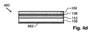
図1dは、本発明の第1の態様による色変換装置180の別の実施形態を模式的に示す。色変換装置180は、第1のルミネッセント層110、グラフェン層108、及び第2のルミネッセント層182のスタックが上に設けられる支持層106を含む。グラフェン層108は、第1のルミネッセント層110と第2のルミネッセント層182との間に挟持される。第1のルミネッセント層110は、特徴が上述されたルミネッセント材料を含む。第2のルミネッセント層182は、第1の色の光を含む第3のスペクトル分布の光の一部(色変換装置180によって受け取られている光)を吸収する及び/又は第2のスペクトル分布の光の一部(第1のルミネッセント層110によって放射されている)を吸収するように構成された第2のルミネッセント材料を含み、第2のルミネッセント材料は、吸収された光の一部を第4のスペクトル分布の光へと変換するように構成される。ある特定の実施形態では、第3のスペクトル分布は、第1のスペクトル分布とは異なり、別の実施形態では、それらは等しい。別の特定の実施形態では、第4のスペクトル分布は、第2のスペクトル分布と等しい。
FIG. 1d schematically illustrates another embodiment of a
図1dの実施形態では、2つの異なるルミネッセント材料が設けられる事に留意されたい。特定の実施形態では、色変換装置は、3つ以上のルミネッセント材料を含み得る。追加のルミネッセント材料は、追加の別々の層に設けられてもよい又は第1のルミネッセント材料及び/若しくは第2のルミネッセント材料として同じ層に設けられてもよい。他に提示される色変換装置の実施形態では、そのような追加のルミネッセント層を使用してもよい及び/又はルミネッセント材料の混合を使用してもよい。 Note that in the embodiment of FIG. 1d, two different luminescent materials are provided. In certain embodiments, the color conversion device may include more than two luminescent materials. The additional luminescent material may be provided in an additional separate layer or may be provided in the same layer as the first luminescent material and / or the second luminescent material. Other presented color conversion device embodiments may use such additional luminescent layers and / or use a mixture of luminescent materials.
(第1の)グラフェン層108及び任意選択の第2のグラフェン層162は、「グラフェン」という用語で示される材料から作られる。グラフェンは、原子スケールハニカム格子の炭素原子の単層を含む又はそのような原子スケールハニカム格子の炭素原子の単層を2〜9含む材料である。ハニカム格子の炭素原子が9層を超えると、材料の特徴が大幅に変化し、「グラファイト」という材料の話題となる。本発明の状況では、グラフェンは、熱伝導性及び光透過性(これは、材料に衝突する光のかなりの部分が材料を透過する事を意味する)でなければならず、従って、グラフェンは、原子スケールハニカム格子の1〜9の炭素原子層を有し得る。
The (first)
グラフェンは、良好な熱導体であり、グラフェン層が比較的少数の層を有する場合、それは、ほぼ透明であり、従って、光を非常に良く透過させる。その結果、上述の実施形態のグラフェン層は、色変換装置内でのより良好な熱拡散に貢献する。この事は、ルミネッセント材料が高過ぎる温度によって破壊又は劣化されないので、ルミネッセント材料のより良好な作用及びルミネッセント材料のより長い寿命をもたらす。 Graphene is a good thermal conductor, and if the graphene layer has a relatively small number of layers, it is almost transparent and therefore transmits light very well. As a result, the graphene layer of the above-described embodiment contributes to better thermal diffusion in the color conversion device. This results in a better action of the luminescent material and a longer lifetime of the luminescent material, since the luminescent material is not destroyed or degraded by temperatures that are too high.
(第1の)ルミネッセント層110及び/又は第2のルミネッセント層182はそれぞれ、無機蛍光体、有機蛍光体、並びに量子閉じ込めを示す及び少なくとも1つの寸法においてナノメートル領域のサイズを有する粒子の群から選択されたルミネッセント材料を含む。
Each of the (first)
無機ルミネッセント材料は、YAG及び/若しくはLuAG等の黄色若しくは黄色/緑色発光無機蛍光体、又はECAS及び/若しくはBSSN等の赤色無機蛍光体を含んでもよい。 The inorganic luminescent material may comprise a yellow or yellow / green emitting inorganic phosphor such as YAG and / or LuAG, or a red inorganic phosphor such as ECAS and / or BSSN.
ルミネッセント材料として適した無機蛍光体の例は、セリウムドープイットリウムアルミニウムガーネット(Y3Al5O12:Ce3+、YAG:Ce若しくはCeドープYAGとも呼ばれる)又はルテチウムアルミニウムガーネット(LuAG、Lu3Al5O12)、α−SiAlON:Eu2+(黄色)、及びM2Si5N8:Eu2+(赤色)(Mは、カルシウムCa、Sr、及びBaから選択された少なくとも1つの元素である)を含むが、これらに限定されない。更に、アルミニウムの一部は、ガドリニウム(Gd)又はガリウム(Ga)に置き換えられてもよく、Gdが多い程、黄色発光の赤色シフトをもたらす。他の適切な材料は、赤色領域の光を放射するSr2Si5N8:Eu2+等の(Sr1−x−yBaxCay)2−zSi5−aAlaN8−aOa:Euz 2+(0≦a<5、0≦x≦1、0≦y≦1、0<z≦1、及び(x+y)≦1)を含み得る。 Examples of suitable inorganic phosphors as luminescent materials cerium doped yttrium aluminum garnet (Y 3 Al 5 O 12: Ce 3+, YAG: Ce or also called Ce-doped YAG) or lutetium aluminum garnet (LuAG, Lu 3 Al 5 O 12 ), α-SiAlON: Eu 2+ (yellow), and M 2 Si 5 N 8 : Eu 2+ (red), where M is at least one element selected from calcium Ca, Sr, and Ba However, it is not limited to these. Furthermore, a part of aluminum may be replaced with gadolinium (Gd) or gallium (Ga), and the more Gd, the more the red shift of yellow emission occurs. Other suitable materials, the red region of the emitting light Sr 2 Si 5 N 8: Eu 2+ or the like of the (Sr 1-x-y Ba x Ca y) 2-z Si 5-a Al a N 8-a O a : Eu z 2+ (0 ≦ a <5, 0 ≦ x ≦ 1, 0 ≦ y ≦ 1, 0 <z ≦ 1, and (x + y) ≦ 1).
無機蛍光体の粒子は、例えば、ポリメチルメタクリレート(PMMA)、ポリエチレンテレフタレート(PET)、ポリエチレンナフタレート(PEN)、又はポリカーボネート(PC)等のマトリックスポリマーに分散されてもよい。無機蛍光体は、シリコーン又は他のエポキシ樹脂及び/若しくは樹脂に分散されてもよい。他の実施形態では、無機蛍光体は、セラミックルミネッセント層の基礎を形成する。 The inorganic phosphor particles may be dispersed in a matrix polymer such as polymethyl methacrylate (PMMA), polyethylene terephthalate (PET), polyethylene naphthalate (PEN), or polycarbonate (PC). The inorganic phosphor may be dispersed in silicone or other epoxy resin and / or resin. In other embodiments, the inorganic phosphor forms the basis of a ceramic luminescent layer.
有機蛍光体は、高量子効率を有する及び多くの場合透明であり、これは、望ましくない散乱を防止する及び効率を向上させる。有機ルミネッセント材料は、更なる利点を有する。発光スペクトルの位置及び帯域幅は、可視領域内のどこにでも容易に設計する事ができる。そのため、高有効性で白色光を放射する光源を製造する事が比較的簡単である。白色光は、少なくとも2色の光の組み合わせでもよく、従って、光源は、第1の色の光を放射する単一の発光体及び第1の色の光の一部を第2の色の光へと変換する少なくとも1つの有機ルミネッセント材料を含み得る。 Organic phosphors have high quantum efficiency and are often transparent, which prevents unwanted scattering and improves efficiency. Organic luminescent materials have a further advantage. The position and bandwidth of the emission spectrum can be easily designed anywhere in the visible region. Therefore, it is relatively easy to manufacture a light source that emits white light with high effectiveness. White light may be a combination of at least two colors of light, so that the light source is a single emitter that emits light of the first color and a portion of the light of the first color is light of the second color. At least one organic luminescent material that converts to
有機蛍光体は、黄色発光ペリレン誘導体又は赤色/橙色発光ペリレン誘導体等のペリレン誘導体を含む材料でもよい。このようなペリレン誘導体は、Lumogen Yellow F083又はF170、Lumogen Red F305、及びLumogen Orange F240の名称で市販されている。 The organic phosphor may be a material containing a perylene derivative such as a yellow light emitting perylene derivative or a red / orange light emitting perylene derivative. Such perylene derivatives are commercially available under the names Lumogen Yellow F083 or F170, Lumogen Red F305, and Lumogen Orange F240.
このような有機ルミネッセント材料又は染料には、ほぼ無尽蔵の品揃えがある。関連する例は、ペリレン(ドイツのLudwigshafenにある企業BASFの商品名Lumogenで知られる染料等:Lumogen F240 Orange、Lumogen F300 Red、Lumogen F305 Red、Lumogen F083 Yellow、Lumogen F170 Yellow、Lumogen F850 Green)、インドのMumbaiにある企業Neelikon Food Dyes & Chemical Ltd.のYellow 172、及び多くの業者から入手可能な、クマリン(例えば、Coumarin 6、Coumarin 7、Coumarin 30、Coumarin 153、Basic Yellow 51)、ナフタルイミド(例えば、Solvent Yellow 11、Solvent Yellow 116)、Fluorol 7GA、ピリジン(例えばpyridine 1)、ピロメテン(Pyrromethene 546、Pyrromethene 567等)、ウラニン、ローダミン(例えば、Rhodamine 110、Rhodamine B、Rhodamine 6G、Rhodamine 3B、Rhodamine 101、Sulphorhodamine 101、Sulphorhodamine 640、Basic Violet 11、Basic Red 2)、シアニン(例えば、フタロシアニン、DCM)、スチルベン(例えばBis−MSB、DPS)である。酸性染料、塩基性染料、直接染料、及び分散染料等の他の幾つかの染料は、それらが使用目的にとって十分に高い蛍光量子収率を示す限り使用する事ができる。従って、ルミネッセント部分の1つ又は複数は、ペリレン基を含み得る。特に、1つ又は複数のルミネッセント部分は、青色及び/又はUV光によって励起されると、赤色ルミネッセンスを生成するように構成される。
Such organic luminescent materials or dyes have an almost infinite assortment. Related examples are perylene (dyes known under the trade name Lumogen of the company BASF in Ludwigshafen, Germany: Lumogen F240 Orange, Lumogen F300 Red, Lumogen F305 Red, Lumogen F083 Yellow, Lumogen F170 Yellow, Lumogen F850 Green), India Yellow 172 from Neelikon Food Dyes & Chemical Ltd. in Mumbai, and coumarins (eg Coumarin 6, Coumarin 7, Coumarin 30, Coumarin 153, Basic Yellow 51), naphthalimide (eg , Solvent Yellow 11, Solvent Yellow 116), Fluorol 7GA, pyridine (eg, pyridine 1), pyromethene (Pyrromethene 546, Pyrromethene 567, etc.), uranin, rhodamine (eg,
有機蛍光体の分子は、例えば、ポリメチルメタクリレート(PMMA)、ポリエチレンテレフタレート(PET)、ポリエチレンナフタレート(PEN)、又はポリカーボネート(PC)等のマトリックスポリマーに溶解されてもよい。有機蛍光体の分子は、シリコーン又はエポキシ樹脂若しくは樹脂に溶解されてもよい。 The molecules of the organic phosphor may be dissolved in a matrix polymer such as polymethyl methacrylate (PMMA), polyethylene terephthalate (PET), polyethylene naphthalate (PEN), or polycarbonate (PC). The organic phosphor molecules may be dissolved in silicone or epoxy resin or resin.
量子閉じ込めを示す及び少なくとも1つの寸法においてナノメートル領域のサイズを有する粒子は、例えば、量子ドット、量子ロッド、又は量子テトラポッドである。1つの寸法においてナノメートル領域のサイズを有するとは、例えば粒子が実質的に球状である場合に、それらの直径がナノメートル領域にある事を意味する。又は、これは、例えばそれらがワイヤ形状である場合に、ワイヤの断面のサイズが1方向においてナノメートル領域にある事を意味する。ナノメートル領域のサイズとは、それらのサイズが少なくとも1マイクロメートル未満(従って、500ナノメートル未満及び0.5ナノメートル以上)である事を意味する。ある実施形態では、1つの寸法におけるサイズは、50ナノメートル未満である。別の実施形態では、1つの寸法におけるサイズは、2〜30ナノメートルの範囲にある。量子ドットは、通常ほんの数ナノメートルの幅又は直径を有する半導体材料の小さな結晶である。入射光によって励起されると、量子ドットは、結晶のサイズ及び材料によって決定される色の光を放射する。従って、ドットのサイズを適合させる事によって、特定の色の光を生み出す事ができる。可視領域で発光する最も良く知られた量子ドットは、硫化カドミウム(CdS)及び硫化亜鉛(ZnS)等の殻を有するセレン化カドミウム(CdSe)に基づく。リン化インジウム(InP)、硫化銅インジウム(CuInS2)及び/又は硫化銀インジウム(AgInS2)等のカドミウムを含まない量子ドットも使用する事ができる。量子ドットは、非常に狭い発光帯を示し、従って、それらは飽和色を示す。更に、発光色は、量子ドットのサイズを適合させる事によって簡単に調整する事ができる。当該分野で公知のどのような種類の量子ドットも、それが適切な波長変換特性を有するならば、本発明において使用する事ができる。 Particles that exhibit quantum confinement and have a size in the nanometer range in at least one dimension are, for example, quantum dots, quantum rods, or quantum tetrapods. Having a size in the nanometer range in one dimension means that their diameter is in the nanometer range, for example when the particles are substantially spherical. Or this means that the wire cross-sectional size is in the nanometer region in one direction, for example when they are wire-shaped. The size of the nanometer region means that their size is at least less than 1 micrometer (and thus less than 500 nanometers and 0.5 nanometers or more). In certain embodiments, the size in one dimension is less than 50 nanometers. In another embodiment, the size in one dimension is in the range of 2-30 nanometers. Quantum dots are small crystals of semiconductor material that usually have a width or diameter of only a few nanometers. When excited by incident light, the quantum dots emit light of a color determined by the crystal size and material. Therefore, a specific color of light can be produced by adapting the dot size. The best known quantum dots emitting in the visible region are based on cadmium selenide (CdSe) with shells such as cadmium sulfide (CdS) and zinc sulfide (ZnS). Quantum dots not containing cadmium such as indium phosphide (InP), copper indium sulfide (CuInS 2 ) and / or silver indium sulfide (AgInS 2 ) can also be used. Quantum dots exhibit a very narrow emission band and therefore they exhibit a saturated color. Furthermore, the emission color can be easily adjusted by adapting the size of the quantum dots. Any type of quantum dot known in the art can be used in the present invention provided it has suitable wavelength conversion properties.
色変換装置によって放射される光の演色評価数(CRI:color rendering index)を向上させる為に、異なるルミネッセント材料の組み合わせを使用する事ができる。ルミネッセント材料の多層スタックを使用してもよい又は異なるルミネッセント材料を単一層において混ぜ合わせてもよい。層スタックの層間で熱を拡散させる為に、グラフェン層を求めてもよい。更に、ルミネッセント層の代替の配置では、層は、例えばピクセル化されたルミネッセント層において等、空間的に分離された異なる材料を含む。 Combinations of different luminescent materials can be used to improve the color rendering index (CRI) of the light emitted by the color conversion device. A multilayer stack of luminescent materials may be used, or different luminescent materials may be mixed in a single layer. A graphene layer may be sought to diffuse heat between layers of the layer stack. Further, in alternative arrangements of luminescent layers, the layers include different materials that are spatially separated, such as in a pixelated luminescent layer.
ルミネッセント材料層の製造方法及びそれらを例えば支持層等の他の層に貼り付ける方法は、当業者には周知である。比較的大きな領域へのグラフェン層の貼り付けは、例えばNano Lett. 2009, 9(12), pp 4359-4363に発表され、American Chemical Societyによって発行された、X. Li et al, “Transfer of large-area graphene films for high-performance transparent conductive electrodes”の論文に記載されている。 Methods for producing luminescent material layers and methods for attaching them to other layers such as support layers are well known to those skilled in the art. The attachment of graphene layers to relatively large areas has been published in, for example, Nano Lett. 2009, 9 (12), pp 4359-4363 and published by the American Chemical Society, X. Li et al, “Transfer of large -area graphene films for high-performance transparent conductive electrodes ".
図2は、照明ユニット200の一実施形態を模式的に示す。照明ユニットは、ハウジング、2つの固体発光体206、及び図1bの色変換装置を含む。ハウジングは、ベース208及び壁202を含み、壁202及びベース208は、キャビティ204を包囲する。ハウジングは、光出射窓216を更に含む。図1bの色変換装置は、光出射窓216に設けられる。ハウジングの少なくとも一部は、熱伝導性材料から作られる。図2の例では、少なくとも壁202は、例えば金属等の熱伝導性材料から作られる。ベース208は、同じ材料から作られてもよい。色変換装置は、グラフェン層108、支持層106、及びルミネッセント層110を含む。色変換装置の横側面端部142は、色変換装置から出るように熱を輸送する事によって、色変換装置の温度を低下させる事ができるように、熱伝導性材料の壁202に熱的に結合される。色変換装置に向けて第1の色の光210を放射する2つの固体発光体206は、ベース208上のキャビティ204内に設けられる。固体発光体206は、例えば発光ダイオードである。ある任意選択的実施形態では、固体発光体206は、固体発光体206において生成された熱をそれらから出るように伝導する事ができるように、熱的にベース208に結合される。第1の色の光210は、グラフェン層108を通り、支持層106を通って透過し、そして、ルミネッセント層110のルミネッセント材料によって少なくとも部分的に吸収される。ルミネッセント材料は、吸収された光の少なくとも一部を特定の分布の光212へと変換する。図2に示されるように、光出射窓216を通って放射された光は、第1の色の光210及び特定のスペクトル分布の光212を含む。ルミネッセント材料によって吸収された第1の色の光210の(相対)量に応じて、照明ユニット200によって特定の色の光を放射する事ができ、特定の色は、第1の色の光210及び特定のスペクトル分布の光212を混ぜ合わせる事によって得る事ができる。どの位の第1の色の光210が吸収されているかは、例えば、特定のルミネッセント材料、ルミネッセント層110に使用されたルミネッセント材料の量、及びルミネッセント層110の厚さによって決まる。
FIG. 2 schematically shows an embodiment of the
照明ユニット200では、ルミネッセント層110において、熱が局所的に生成される。グラフェン層108は、支持層106を介して、ルミネッセント層110に熱的に結合される。グラフェンは、良好な熱導体であり、グラフェン層108によって受け取られた熱は、色変換装置内で熱がより良く分布される及びルミネッセント層110内の最大温度が低下されるように、横方向に伝導される。グラフェン層108は、色変換装置で生成されている熱が照明ユニット200のハウジングに向けて伝導されてルミネッセント層110の最大温度を更に低下する事ができるように、照明ユニット200の壁202にも熱的に結合される。
In the
図2は、照明ユニット200の断面図を示す事に留意されたい。従って、照明ユニット200の三次元形状は、箱形状又は円筒形状でもよい。更に、この断面図は、2つの固体発光体206を示すが、3つ以上の固体発光体206がキャビティ内に存在してもよい。別の任意選択的実施形態では、照明ユニット200は、単一の固体発光体206を含む。例えば図3a及び3bに示される照明ユニットの他の実施形態は、上述の実施形態に従った形状を有してもよい及び1つ又は複数の固体発光体を含んでもよい。
Note that FIG. 2 shows a cross-sectional view of the
キャビティ204は、例えば空気等の気体で満たされる。照明ユニット200の別の実施形態では、光透過性樹脂がキャビティ内に設けられる並びに固体発光体206及び色変換装置に光学的に結合される。
The
図3aは、ヒートシンク308を含む照明ユニット300の別の実施形態を模式的に示す。照明ユニット300は、図1cの色変換装置を含み、色変換装置は、照明ユニット300のハウジングの光出射窓に設けられる。ハウジングは、キャビティ304を包囲する熱伝導性壁302及び熱伝導性ベース306を含む。色変換装置は、熱伝導性壁302に熱的に結合され、より詳細には、色変換装置の第1のグラフェン層108及び第2のグラフェン層162は、色変換装置から出てヒートシンク308へとルミネッセント層110内で生成された熱を伝導する事ができるように、熱伝導性壁302に熱的に結合される。キャビティ304から見て外方に向くベースの表面において、例えばフィンを含むヒートシンク308が設けられる。色変換装置の他の特徴は、図2の照明ユニット200の特徴と同様である。照明ユニット300の示された実施形態は、図1cの色変換装置に限定されない事に留意されたい。光出射窓において、他の色変換装置が設けられてもよい。
FIG. 3 a schematically illustrates another embodiment of a
任意選択的に、色変換装置に設けられたグラフェン層108、162に加えて、照明ユニット300は、発光体206に熱的に結合される及びハウジングの熱伝導性部分に熱的に結合される、キャビティ304内に設けられる追加のグラフェン層310を含んでもよい。図3aの例では、追加のグラフェン層310は、熱伝導性ベース306の上に設けられ、固体発光体206及びベース306に接触する。その結果、グラフェン層310は、固体発光体206から生じた熱を照明ユニット300の他の部分(図3aの例ではヒートシンク308等)に向けて拡散する助けとなる。例えば図2及び図3bに示される様な照明ユニットの他の実施形態は、照明ユニット内で追加の熱の拡散及び伝導を提供する為にキャビティ内に1つ又は複数の追加のグラフェン層を含んでもよい事に留意されたい。図3aでは、追加のグラフェン層310は、ベース306の上に設けられた及び固体発光体206の上には施されていない層としてのみ描かれている。しかしながら、ある代替実施形態では、追加のグラフェン層310は、より良好な熱接触が得られるように、固体発光体206の上にも設けられる。
Optionally, in addition to the graphene layers 108, 162 provided in the color conversion device, the
図3bは、ドーム型発光体ダイオード358/360を含む照明ユニット350の更なる実施形態を模式的に示す。照明ユニット350は、上述の照明ユニットに類似する。図3bの照明ユニット350の具体例では、図1dの色変換装置は、照明ユニット350のハウジングの光出射窓に設けられている。照明ユニット350のハウジングは、熱伝導性壁352及び熱伝導性ベース356のハウジングを含む。色変換装置は、熱伝導性壁352に熱的に結合される。ハウジングは、空気で満たされたキャビティ354を包囲する。キャビティ354内では、ベース356の表面上に、発光ダイオード360が設けられ、これらは、対応する発光ダイオード360によって放射された光を所定の光線へと屈折させるドーム358を備える。ドーム358は、レンズに似た機能を有し得るが、少なくとも、発光ダイオード360ダイからの光のアウトカップリングを向上させる為に使用される。
FIG. 3b schematically illustrates a further embodiment of a
図4a〜図4dは、色変換装置の代替実施形態の断面図を模式的に示す。図4aは、図1bの色変換装置140に類似した及び追加の第2のグラフェン層402を含む色変換装置400を示す。第2のグラフェン層402は、ルミネッセント層110が支持層106と接触する面とは反対側のルミネッセント層110の面上に設けられる。従って、色変換装置400の平面に対して垂直な方向に見た場合、色変換装置400は、層:第1のグラフェン層108、支持層106、ルミネッセント層110及び第2のグラフェン層402から構築される。
4a to 4d schematically show cross-sectional views of alternative embodiments of the color conversion device. FIG. 4 a shows a
図4bは、図1cの色変換装置160に類似した色変換装置420を示す。追加の第3のグラフェン層422は、第1のグラフェン層108、第1のルミネッセント層110、及び第2のグラフェン層162のスタックが設けられる支持層106の表面とは反対側の支持層106の表面に設けられる。従って、色変換装置420の平面に対して垂直な方向に見た場合、色変換装置420は、層:第3のグラフェン層422、支持層106、第1のグラフェン層108、ルミネッセント層110及び第2のグラフェン層162から構築される。
FIG. 4b shows a
図4cは、図1dの色変換装置180に類似した色変換装置440を示す。追加の第2のグラフェン層442は、第1のグラフェン層108と接触する第2のルミネッセント層182の表面とは反対側の第2のルミネッセント層182の表面に設けられる。従って、色変換装置440の平面に対して垂直な方向に見た場合、色変換装置440は、層:支持層106、第1のルミネッセント層110、第1のグラフェン層108、第2のルミネッセント層182及び第2のグラフェン層442から構築される。
FIG. 4c shows a
図4dは、図1dの色変換装置180に類似した色変換装置460を示す。追加の第2のグラフェン層462は、第1のルミネッセント層110と接触する支持層106の表面とは反対側の支持層106の表面に設けられる。従って、色変換装置460の平面に対して垂直な方向に見た場合、色変換装置460は、層:第2のグラフェン層462、支持層106、第1のルミネッセント層110、第1のグラフェン層108及び第2のルミネッセント層182から構築される。
FIG. 4d shows a
図5は、照明器具500の一実施形態を模式的に示す。照明器具500は、図1a〜図1d若しくは図4a〜図4dに関連して開示された少なくとも1つの色変換装置を含む、及び/又は図2若しくは図3a及び図3bに関連して開示された少なくとも1つの照明ユニットを含む。
FIG. 5 schematically illustrates one embodiment of a
要約すると、本出願は、色変換装置、照明ユニット、固体発光体パッケージ、照明器具、及びグラフェン層の特定の使用を提供する。第1の態様を有する色変換装置は、第1のルミネッセント層、支持層及び第1のグラフェン層を含む。色変換装置は、第1の色の光を別の色の光に変換する為のものである。第1のルミネッセント層は、第1の色を含む第1のスペクトル分布の光の一部を吸収し、吸収された光の少なくとも一部を第2のスペクトル分布の光へと変換する第1のルミネッセント材料を含む。支持層は、ルミネッセント層を支持する。第1のグラフェン層は、色変換装置内の温度差が低減されるように、熱を横方向に熱伝導する。色変換装置の層の異なる構成が提供される。 In summary, the present application provides specific uses of color conversion devices, lighting units, solid state light emitter packages, lighting fixtures, and graphene layers. The color conversion device having the first aspect includes a first luminescent layer, a support layer, and a first graphene layer. The color conversion device is for converting light of a first color into light of another color. The first luminescent layer absorbs a portion of the light having the first spectral distribution including the first color and converts at least a portion of the absorbed light into light having the second spectral distribution. Contains luminescent material. The support layer supports the luminescent layer. The first graphene layer conducts heat laterally so that a temperature difference in the color conversion device is reduced. Different configurations of the layers of the color conversion device are provided.
上述の実施形態が本発明を限定するのではなく例示する事、及び当業者は添付のクレームの範囲から逸脱する事なく多くの代替実施形態を設計できる事に留意されたい。 It should be noted that the above-described embodiments illustrate rather than limit the invention, and that those skilled in the art can design many alternative embodiments without departing from the scope of the appended claims.
クレームにおいて、丸括弧内の何れの参照符号もクレームを限定するものと解釈されるものではない。「含む」(“comprise”)という動詞及びその活用形の使用は、クレームに記載されたもの以外の要素又はステップの存在を排除しない。要素に先行する冠詞「a」又は「an」は、複数のそのような要素の存在を排除しない。本発明は、幾つかの異なる要素を含むハードウェアを用いて及び適切にプログラムされたコンピュータを用いて実施され得る。幾つかの手段を列挙する装置クレームでは、これらの手段の幾つかは、ハードウェアの同一のアイテムによって具現化されてもよい。特定の方策が互いに異なる従属クレームに記載されているという事実だけでは、これらの方策の組み合わせを有利に使用できない事を意味しない。 In the claims, any reference signs placed between parentheses shall not be construed as limiting the claim. Use of the verb “comprise” and its conjugations does not exclude the presence of elements or steps other than those stated in a claim. The article “a” or “an” preceding an element does not exclude the presence of a plurality of such elements. The present invention may be implemented using hardware including several different elements and using a suitably programmed computer. In the device claim enumerating several means, several of these means may be embodied by one and the same item of hardware. The fact that certain measures are described in different dependent claims does not mean that a combination of these measures cannot be used to advantage.
Claims (11)
前記キャビティ内に設けられ、第1の色の光を放射する発光体と、
前記第1の色の光を別の色の光へと変換する色変換装置と、
を含む照明ユニットであって、前記色変換装置は、
前記第1の色を含む第1のスペクトル分布の光の一部を吸収する及び前記吸収された光の少なくとも一部を第2のスペクトル分布の光へと変換する第1のルミネッセント材料を含む第1のルミネッセント層と、
前記第1のルミネッセント層を支持する支持層と、
前記色変換装置内の温度差を低減するための第1のグラフェン層と、
を含み、
i)前記支持層は、固体発光体の層によって形成され、前記第1のルミネッセント層及び前記第1のグラフェン層のスタックは、前記固体発光体の層上に設けられ、前記固体発光体の層の発光面は、前記第1のルミネッセント層若しくは前記第1のグラフェン層の何れかと接触するか、
ii)前記支持層は、第1の面及び前記第1の面とは反対側の第2の面を含み、前記第1のグラフェン層は、前記支持層の前記第1の面に設けられ、前記第1のグラフェン層は、前記支持層に熱的に結合され、前記第1のルミネッセント層は、前記支持層の前記第2の面に設けられ、前記第1のルミネッセント層は、前記支持層に熱的に結合されるか、
iii)前記色変換装置は、第2のグラフェン層を含み、前記第1のルミネッセント層は、前記第1のグラフェン層と前記第2のグラフェン層との間に挟持され、前記グラフェン層及び前記第1のルミネッセント層のスタックは、前記支持層上に設けられるか、又は
iv)前記色変換装置は、前記第1の色を含む第3のスペクトル分布の光及び/若しくは前記第2のスペクトル分布の光の一部を吸収する及び吸収された光の少なくとも一部を第4のスペクトル分布の光へと変換する第2のルミネッセント材料を含む第2のルミネッセント層を含み、前記第1のグラフェン層は、前記第1のルミネッセント層と前記第2のルミネッセント層との間に挟持され、前記ルミネッセント層及び前記第1のグラフェン層のスタックは、前記支持層上に設けられ、
前記色変換装置は前記光出射窓に設けられ、前記第1のグラフェン層及び/又は前記第2のグラフェン層が前記熱伝導性材料の前記ハウジングの少なくとも一部に熱的に結合される、照明ユニット。 A housing including a light exit window and surrounding the cavity, wherein at least a portion of the housing is made of a thermally conductive material;
A light emitter provided in the cavity and emitting light of a first color;
A color conversion device for converting the light of the first color into light of another color;
The color conversion device includes:
A first luminescent material that absorbs a portion of light of a first spectral distribution that includes the first color and that converts at least a portion of the absorbed light into light of a second spectral distribution; A luminescent layer,
A support layer that supports the first luminescent layer;
A first graphene layer for reducing a temperature difference in the color conversion device;
Including
i) The support layer is formed by a layer of a solid light emitter, and the stack of the first luminescent layer and the first graphene layer is provided on the layer of the solid light emitter, and the layer of the solid light emitter The light emitting surface of the light emitting surface is in contact with either the first luminescent layer or the first graphene layer,
ii) The support layer includes a first surface and a second surface opposite to the first surface, and the first graphene layer is provided on the first surface of the support layer; The first graphene layer is thermally coupled to the support layer, the first luminescent layer is provided on the second surface of the support layer, and the first luminescent layer is the support layer. Thermally coupled to
iii) The color conversion device includes a second graphene layer, and the first luminescent layer is sandwiched between the first graphene layer and the second graphene layer, and the graphene layer and the first graphene layer A stack of one luminescent layer is provided on the support layer, or iv) the color conversion device comprises light of a third spectral distribution containing the first color and / or of the second spectral distribution A second luminescent layer comprising a second luminescent material that absorbs a portion of the light and converts at least a portion of the absorbed light into light of a fourth spectral distribution, wherein the first graphene layer comprises: A stack of the luminescent layer and the first graphene layer is provided on the support layer. The stack of the luminescent layer and the first graphene layer is disposed between the first luminescent layer and the second luminescent layer. And
The color conversion device is provided in the light exit window, and the first graphene layer and / or the second graphene layer is thermally coupled to at least a portion of the housing of the thermally conductive material unit.
前記色変換装置が前記第2のグラフェン層を含み、前記第1のルミネッセント層が前記第1のグラフェン層と前記第2のグラフェン層との間に挟持され、前記グラフェン層及び前記第1のルミネッセント層の前記スタックが前記支持層上に設けられる場合、又は
前記色変換装置が前記第2のルミネッセント材料を含む前記第2のルミネッセント層を含み、前記第1のグラフェン層が前記第1のルミネッセント層と前記第2のルミネッセント層との間に挟持され、前記ルミネッセント層及び前記第1のグラフェン層の前記スタックが前記支持層上に設けられる場合に、
前記反対側の表面は、前記スタックの1つが上に設けられる表面とは反対側の前記支持層の表面であり、
前記色変換装置は前記光出射窓に設けられ、前記第1のグラフェン層及び前記別の第2のグラフェン層が前記熱伝導性材料の前記ハウジングの少なくとも一部に熱的に結合される、請求項1に記載の照明ユニット。 The color conversion device includes another second graphene layer provided on a surface opposite to the support layer,
The color conversion device includes the second graphene layer, the first luminescent layer is sandwiched between the first graphene layer and the second graphene layer, and the graphene layer and the first luminescent layer are sandwiched between the first graphene layer and the second graphene layer. When the stack of layers is provided on the support layer, or the color conversion device comprises the second luminescent layer comprising the second luminescent material, and the first graphene layer comprises the first luminescent layer And the second luminescent layer, and the stack of the luminescent layer and the first graphene layer is provided on the support layer,
The opposite surface is the surface of the support layer opposite the surface on which one of the stacks is provided;
The color conversion device is provided in the light exit window, and the first graphene layer and the second second graphene layer are thermally coupled to at least a portion of the housing of the thermally conductive material. Item 2. The lighting unit according to Item 1.
前記色変換装置が前記第2のルミネッセント材料を含む前記第2のルミネッセント層を含み、前記第1のグラフェン層が前記第1のルミネッセント層と前記第2のルミネッセント層との間に挟持され、前記ルミネッセント層及び前記第1のグラフェン層の前記スタックが前記支持層上に設けられる場合に、
前記色変換装置は、それぞれ前記第1のルミネッセント層の表面上若しくは前記支持層から見て外方に向く前記第2のルミネッセント層の表面上に設けられる、更なる第2のグラフェン層を含み、
前記色変換装置は前記光出射窓に設けられ、前記第1のグラフェン層及び前記更なる第2のグラフェン層が前記熱伝導性材料の前記ハウジングの少なくとも一部に熱的に結合される、請求項1に記載の照明ユニット。 The support layer includes the first surface and the second surface opposite to the first surface; the first graphene layer is provided on the first surface of the support layer; One graphene layer is thermally coupled to the support layer, the first luminescent layer is provided on the second surface of the support layer, and the first luminescent layer is thermally coupled to the support layer Or the color conversion device includes the second luminescent layer including the second luminescent material, and the first graphene layer is between the first luminescent layer and the second luminescent layer. When the stack of the luminescent layer and the first graphene layer is provided on the support layer,
The color conversion device includes a further second graphene layer provided on the surface of the first luminescent layer or the surface of the second luminescent layer facing outward from the support layer, respectively.
The color conversion device is provided in the light exit window, and the first graphene layer and the further second graphene layer are thermally coupled to at least a portion of the housing of the thermally conductive material. Item 2. The lighting unit according to Item 1.
前記第1の色を含む第1のスペクトル分布の光の一部を吸収する及び前記吸収された光の少なくとも一部を第2のスペクトル分布の光へと変換する第1のルミネッセント材料を含む第1のルミネッセント層と、
前記第1のルミネッセント層を支持する支持層と、
前記色変換装置内の温度差を低減するための第1のグラフェン層と、
を含み、
ii)前記支持層は、第1の面及び前記第1の面とは反対側の第2の面を含み、前記第1のグラフェン層は、前記支持層の前記第1の面に設けられ、前記第1のグラフェン層は、前記支持層に熱的に結合され、前記第1のルミネッセント層は、前記支持層の前記第2の面に設けられ、前記第1のルミネッセント層は、前記支持層に熱的に結合されるか、又は
iv)前記色変換装置は、前記第1の色を含む第3のスペクトル分布の光及び/若しくは前記第2のスペクトル分布の光の一部を吸収する並びに吸収された光の少なくとも一部を第4のスペクトル分布の光へと変換する第2のルミネッセント材料を含む第2のルミネッセント層を含み、前記第1のグラフェン層は、前記第1のルミネッセント層と前記第2のルミネッセント層との間に挟持され、前記ルミネッセント層及び前記第1のグラフェン層のスタックは、前記支持層上に設けられる、色変換装置。 A color conversion device that converts light of a first color into light of another color, the color conversion device comprising:
A first luminescent material that absorbs a portion of light of a first spectral distribution that includes the first color and that converts at least a portion of the absorbed light into light of a second spectral distribution; A luminescent layer,
A support layer that supports the first luminescent layer;
A first graphene layer for reducing a temperature difference in the color conversion device;
Including
ii) The support layer includes a first surface and a second surface opposite to the first surface, and the first graphene layer is provided on the first surface of the support layer; The first graphene layer is thermally coupled to the support layer, the first luminescent layer is provided on the second surface of the support layer, and the first luminescent layer is the support layer. Or iv) the color conversion device absorbs light of the third spectral distribution including the first color and / or part of the light of the second spectral distribution; and A second luminescent layer comprising a second luminescent material that converts at least a portion of the absorbed light into light of a fourth spectral distribution, wherein the first graphene layer includes the first luminescent layer and Sandwiched between the second luminescent layer And a stack of the luminescent layer and the first graphene layer is provided on the support layer.
請求項9に記載の色変換装置と、
を含む固体発光体パッケージであって、前記支持層は、前記固体発光体の層である又は前記固体発光体ダイが上に設けられる基板である、固体発光体パッケージ。 A solid state light emitter die of a solid state light emitter; and
A color conversion device according to claim 9;
A solid state light emitter package, wherein the support layer is a layer of the solid state light emitter or a substrate on which the solid state light emitter die is provided.
Applications Claiming Priority (3)
| Application Number | Priority Date | Filing Date | Title |
|---|---|---|---|
| US201261733510P | 2012-12-05 | 2012-12-05 | |
| US61/733,510 | 2012-12-05 | ||
| PCT/IB2013/060561 WO2014087318A1 (en) | 2012-12-05 | 2013-12-02 | A color conversion arrangement, a lighting unit, a solid state light emitter package and a luminaire |
Publications (3)
| Publication Number | Publication Date |
|---|---|
| JP2016509681A JP2016509681A (en) | 2016-03-31 |
| JP2016509681A5 JP2016509681A5 (en) | 2017-01-19 |
| JP6388595B2 true JP6388595B2 (en) | 2018-09-12 |
Family
ID=49765618
Family Applications (1)
| Application Number | Title | Priority Date | Filing Date |
|---|---|---|---|
| JP2015546126A Expired - Fee Related JP6388595B2 (en) | 2012-12-05 | 2013-12-02 | Color conversion device, lighting unit, solid state light emitter package, and lighting fixture |
Country Status (5)
| Country | Link |
|---|---|
| US (1) | US10094537B2 (en) |
| EP (1) | EP2929573B1 (en) |
| JP (1) | JP6388595B2 (en) |
| CN (1) | CN104854717B (en) |
| WO (1) | WO2014087318A1 (en) |
Families Citing this family (17)
| Publication number | Priority date | Publication date | Assignee | Title |
|---|---|---|---|---|
| CN103412436B (en) * | 2013-07-24 | 2015-09-30 | 北京京东方光电科技有限公司 | The process for dispersing of a kind of color membrane substrates, LCDs and monochromatic quantum dot |
| US9465165B2 (en) * | 2014-06-30 | 2016-10-11 | Raytheon Company | Reflection/absorption coating for laser slabs |
| US11112653B2 (en) * | 2015-05-29 | 2021-09-07 | Harman International Industries, Incorporated | Wide color-gamut vehicle infotainment display system with quantum dot element |
| US10725227B2 (en) | 2015-05-29 | 2020-07-28 | Harman International Industries, Incorporated | Wide color-gamut vehicle infotainment display system |
| US10656465B2 (en) | 2015-05-29 | 2020-05-19 | Harman International Industries, Incorporated | Wide color-gamut vehicle infotainment display system with quantum dot element |
| TW201721053A (en) * | 2015-12-02 | 2017-06-16 | 羅冠傑 | Shell integrated light-emitting diode, assembly and manufacturing method thereof |
| CN106449618A (en) * | 2016-01-29 | 2017-02-22 | 罗冠杰 | Lamp housing integrated type light emitting diode apparatus and its manufacturing method |
| JP7080010B2 (en) * | 2016-02-04 | 2022-06-03 | 晶元光電股▲ふん▼有限公司 | Light emitting element and its manufacturing method |
| DE102016202071A1 (en) * | 2016-02-11 | 2017-08-17 | Siemens Aktiengesellschaft | Electrical conductor for an electric machine with increased power-to-weight ratio and electrical component for the electric machine |
| JP7029882B2 (en) * | 2016-09-01 | 2022-03-04 | エルジー ディスプレイ カンパニー リミテッド | Light source device and display device |
| CN106653975A (en) * | 2016-12-16 | 2017-05-10 | 华南师范大学 | Chip-level packaging light emitting device and manufacturing method therefor |
| US10611298B2 (en) * | 2017-03-13 | 2020-04-07 | Ford Global Technologies, Llc | Illuminated cargo carrier |
| CN106920867A (en) * | 2017-05-05 | 2017-07-04 | 滁州市量子光电有限公司 | A kind of Graphene luminescence generated by light substrate and its preparation method and application |
| CN107763442A (en) * | 2017-08-15 | 2018-03-06 | 绵阳聚强极风科技有限公司 | A kind of high heat conduction long-life phosphors piece |
| CN112133718B (en) * | 2019-06-25 | 2024-02-20 | 成都辰显光电有限公司 | Display panel, display device and preparation method of display panel |
| US11953194B2 (en) | 2019-08-20 | 2024-04-09 | Signify Holding, B.V. | High quality white laser-based light source by indirect pumping of red phosphor |
| KR20210061858A (en) * | 2019-11-20 | 2021-05-28 | 삼성전자주식회사 | Display apparatus |
Family Cites Families (13)
| Publication number | Priority date | Publication date | Assignee | Title |
|---|---|---|---|---|
| US8410681B2 (en) | 2008-06-30 | 2013-04-02 | Bridgelux, Inc. | Light emitting device having a refractory phosphor layer |
| US20100085713A1 (en) | 2008-10-03 | 2010-04-08 | Balandin Alexander A | Lateral graphene heat spreaders for electronic and optoelectronic devices and circuits |
| US8545033B2 (en) * | 2009-05-28 | 2013-10-01 | Koninklijke Philips N.V. | Illumination device with an envelope enclosing a light source |
| US20110042709A1 (en) | 2009-08-18 | 2011-02-24 | Christoph Stark | Free-standing mounted light emitting diodes for general lighting |
| JP5421751B2 (en) * | 2009-12-03 | 2014-02-19 | スタンレー電気株式会社 | Semiconductor light emitting device |
| CN102386296A (en) | 2010-09-02 | 2012-03-21 | 宋健民 | Graphene transparent electrode, graphene light-emitting diode and preparation method thereof |
| KR20120029269A (en) * | 2010-09-16 | 2012-03-26 | 삼성엘이디 주식회사 | Stack structure including graphene and light emitting device employing the same |
| KR20120032871A (en) * | 2010-09-29 | 2012-04-06 | 삼성전기주식회사 | Radiating substrate and method for manufacturing the radiating substrate, and luminous element package with the radiating structure |
| KR101535463B1 (en) | 2010-11-30 | 2015-07-10 | 삼성전자주식회사 | LED lamp |
| KR20120059061A (en) * | 2010-11-30 | 2012-06-08 | 삼성엘이디 주식회사 | Light emitting device package and method of manufacturing the same |
| KR101184434B1 (en) | 2010-12-15 | 2012-09-20 | 한국과학기술연구원 | Color conversion luminescent sheet and the fabrication method thereof |
| KR101177480B1 (en) | 2011-02-14 | 2012-08-24 | 엘지전자 주식회사 | Lighting apparatus and display device comprising the same |
| KR20120131009A (en) * | 2011-05-24 | 2012-12-04 | 엘지디스플레이 주식회사 | Light emitting device and manufacturing method of the same |
-
2013
- 2013-12-02 CN CN201380063929.2A patent/CN104854717B/en not_active Expired - Fee Related
- 2013-12-02 JP JP2015546126A patent/JP6388595B2/en not_active Expired - Fee Related
- 2013-12-02 US US14/649,328 patent/US10094537B2/en not_active Expired - Fee Related
- 2013-12-02 WO PCT/IB2013/060561 patent/WO2014087318A1/en active Application Filing
- 2013-12-02 EP EP13805601.5A patent/EP2929573B1/en not_active Not-in-force
Also Published As
| Publication number | Publication date |
|---|---|
| CN104854717A (en) | 2015-08-19 |
| EP2929573B1 (en) | 2018-06-13 |
| US10094537B2 (en) | 2018-10-09 |
| CN104854717B (en) | 2017-11-28 |
| EP2929573A1 (en) | 2015-10-14 |
| JP2016509681A (en) | 2016-03-31 |
| WO2014087318A1 (en) | 2014-06-12 |
| US20150345745A1 (en) | 2015-12-03 |
Similar Documents
| Publication | Publication Date | Title |
|---|---|---|
| JP6388595B2 (en) | Color conversion device, lighting unit, solid state light emitter package, and lighting fixture | |
| US9459000B2 (en) | Thermal conductivity and phase transition heat transfer mechanism including optical element to be cooled by heat transfer of the mechanism | |
| US8262257B2 (en) | Illumination device with LED with a self-supporting grid containing luminescent material and method of making the self-supporting grid | |
| JP6305999B2 (en) | Light emitting assembly, lamp and lighting fixture | |
| US9500325B2 (en) | LED lamp incorporating remote phosphor with heat dissipation features | |
| TWI527891B (en) | Phosphor layer having enhanced thermal conduction and light sources utilizing the phosphor layer | |
| JP6231104B2 (en) | Wavelength converter | |
| US10184651B2 (en) | Lighting device with an optical element having a fluid passage | |
| US20130094177A1 (en) | Wavelength conversion component with improved thermal conductive characteristics for remote wavelength conversion | |
| US9952377B2 (en) | Light emitting device with spectral conversion element | |
| JP6434919B2 (en) | Light source, luminaire and surgical lighting unit | |
| JP2015144261A (en) | Solid-state light emitting device with photoluminescence wavelength conversion | |
| US11543577B2 (en) | Luminescent concentrator with CPC, light guide and additional phosphor | |
| JP2014530449A (en) | Light emitting device | |
| TW201417355A (en) | Light emitting arrangement | |
| JP6038398B2 (en) | Light-emitting device for improving cooling | |
| US10001256B2 (en) | Structures subjected to thermal energy and thermal management methods therefor |
Legal Events
| Date | Code | Title | Description |
|---|---|---|---|
| A711 | Notification of change in applicant |
Free format text: JAPANESE INTERMEDIATE CODE: A711 Effective date: 20160912 |
|
| A521 | Request for written amendment filed |
Free format text: JAPANESE INTERMEDIATE CODE: A523 Effective date: 20161201 |
|
| A621 | Written request for application examination |
Free format text: JAPANESE INTERMEDIATE CODE: A621 Effective date: 20161201 |
|
| A977 | Report on retrieval |
Free format text: JAPANESE INTERMEDIATE CODE: A971007 Effective date: 20171031 |
|
| A131 | Notification of reasons for refusal |
Free format text: JAPANESE INTERMEDIATE CODE: A131 Effective date: 20171108 |
|
| A521 | Request for written amendment filed |
Free format text: JAPANESE INTERMEDIATE CODE: A523 Effective date: 20180206 |
|
| TRDD | Decision of grant or rejection written | ||
| A01 | Written decision to grant a patent or to grant a registration (utility model) |
Free format text: JAPANESE INTERMEDIATE CODE: A01 Effective date: 20180717 |
|
| A61 | First payment of annual fees (during grant procedure) |
Free format text: JAPANESE INTERMEDIATE CODE: A61 Effective date: 20180814 |
|
| R150 | Certificate of patent or registration of utility model |
Ref document number: 6388595 Country of ref document: JP Free format text: JAPANESE INTERMEDIATE CODE: R150 |
|
| S531 | Written request for registration of change of domicile |
Free format text: JAPANESE INTERMEDIATE CODE: R313531 |
|
| S533 | Written request for registration of change of name |
Free format text: JAPANESE INTERMEDIATE CODE: R313533 |
|
| R350 | Written notification of registration of transfer |
Free format text: JAPANESE INTERMEDIATE CODE: R350 |
|
| LAPS | Cancellation because of no payment of annual fees |