JP6376029B2 - Signal transmission circuit and switching element drive device - Google Patents
Signal transmission circuit and switching element drive device Download PDFInfo
- Publication number
- JP6376029B2 JP6376029B2 JP2015083318A JP2015083318A JP6376029B2 JP 6376029 B2 JP6376029 B2 JP 6376029B2 JP 2015083318 A JP2015083318 A JP 2015083318A JP 2015083318 A JP2015083318 A JP 2015083318A JP 6376029 B2 JP6376029 B2 JP 6376029B2
- Authority
- JP
- Japan
- Prior art keywords
- signal
- circuit
- period
- input signal
- level
- Prior art date
- Legal status (The legal status is an assumption and is not a legal conclusion. Google has not performed a legal analysis and makes no representation as to the accuracy of the status listed.)
- Expired - Fee Related
Links
- 230000008054 signal transmission Effects 0.000 title claims description 36
- 230000008859 change Effects 0.000 claims description 17
- 230000010355 oscillation Effects 0.000 claims description 4
- 230000007274 generation of a signal involved in cell-cell signaling Effects 0.000 claims description 3
- 230000001172 regenerating effect Effects 0.000 claims 2
- 102100040862 Dual specificity protein kinase CLK1 Human genes 0.000 description 9
- 230000000694 effects Effects 0.000 description 8
- 230000000630 rising effect Effects 0.000 description 8
- 102100040844 Dual specificity protein kinase CLK2 Human genes 0.000 description 6
- 101000749291 Homo sapiens Dual specificity protein kinase CLK2 Proteins 0.000 description 6
- 238000004088 simulation Methods 0.000 description 4
- 101100493897 Arabidopsis thaliana BGLU30 gene Proteins 0.000 description 2
- 101100219315 Arabidopsis thaliana CYP83A1 gene Proteins 0.000 description 2
- 101100422614 Arabidopsis thaliana STR15 gene Proteins 0.000 description 2
- 101000806846 Homo sapiens DNA-(apurinic or apyrimidinic site) endonuclease Proteins 0.000 description 2
- 101000835083 Homo sapiens Tissue factor pathway inhibitor 2 Proteins 0.000 description 2
- 101100269674 Mus musculus Alyref2 gene Proteins 0.000 description 2
- 101100489717 Saccharomyces cerevisiae (strain ATCC 204508 / S288c) GND2 gene Proteins 0.000 description 2
- 101100140580 Saccharomyces cerevisiae (strain ATCC 204508 / S288c) REF2 gene Proteins 0.000 description 2
- 101100141327 Saccharomyces cerevisiae (strain ATCC 204508 / S288c) RNR3 gene Proteins 0.000 description 2
- 102100026134 Tissue factor pathway inhibitor 2 Human genes 0.000 description 2
- 239000003990 capacitor Substances 0.000 description 2
- 101150112501 din1 gene Proteins 0.000 description 2
- 238000010292 electrical insulation Methods 0.000 description 2
- 230000009467 reduction Effects 0.000 description 2
- 101000749294 Homo sapiens Dual specificity protein kinase CLK1 Proteins 0.000 description 1
- 101100489713 Saccharomyces cerevisiae (strain ATCC 204508 / S288c) GND1 gene Proteins 0.000 description 1
- 238000009499 grossing Methods 0.000 description 1
- 230000007257 malfunction Effects 0.000 description 1
- 238000004519 manufacturing process Methods 0.000 description 1
- 230000004048 modification Effects 0.000 description 1
- 238000012986 modification Methods 0.000 description 1
- 230000003071 parasitic effect Effects 0.000 description 1
- 238000011084 recovery Methods 0.000 description 1
- 230000004044 response Effects 0.000 description 1
- 230000007704 transition Effects 0.000 description 1
- 230000001960 triggered effect Effects 0.000 description 1
Images


Classifications
-
- H—ELECTRICITY
- H03—ELECTRONIC CIRCUITRY
- H03K—PULSE TECHNIQUE
- H03K17/00—Electronic switching or gating, i.e. not by contact-making and –breaking
- H03K17/16—Modifications for eliminating interference voltages or currents
- H03K17/168—Modifications for eliminating interference voltages or currents in composite switches
-
- H—ELECTRICITY
- H02—GENERATION; CONVERSION OR DISTRIBUTION OF ELECTRIC POWER
- H02M—APPARATUS FOR CONVERSION BETWEEN AC AND AC, BETWEEN AC AND DC, OR BETWEEN DC AND DC, AND FOR USE WITH MAINS OR SIMILAR POWER SUPPLY SYSTEMS; CONVERSION OF DC OR AC INPUT POWER INTO SURGE OUTPUT POWER; CONTROL OR REGULATION THEREOF
- H02M1/00—Details of apparatus for conversion
- H02M1/08—Circuits specially adapted for the generation of control voltages for semiconductor devices incorporated in static converters
-
- H—ELECTRICITY
- H02—GENERATION; CONVERSION OR DISTRIBUTION OF ELECTRIC POWER
- H02M—APPARATUS FOR CONVERSION BETWEEN AC AND AC, BETWEEN AC AND DC, OR BETWEEN DC AND DC, AND FOR USE WITH MAINS OR SIMILAR POWER SUPPLY SYSTEMS; CONVERSION OF DC OR AC INPUT POWER INTO SURGE OUTPUT POWER; CONTROL OR REGULATION THEREOF
- H02M7/00—Conversion of ac power input into dc power output; Conversion of dc power input into ac power output
- H02M7/42—Conversion of dc power input into ac power output without possibility of reversal
- H02M7/44—Conversion of dc power input into ac power output without possibility of reversal by static converters
- H02M7/48—Conversion of dc power input into ac power output without possibility of reversal by static converters using discharge tubes with control electrode or semiconductor devices with control electrode
- H02M7/53—Conversion of dc power input into ac power output without possibility of reversal by static converters using discharge tubes with control electrode or semiconductor devices with control electrode using devices of a triode or transistor type requiring continuous application of a control signal
- H02M7/537—Conversion of dc power input into ac power output without possibility of reversal by static converters using discharge tubes with control electrode or semiconductor devices with control electrode using devices of a triode or transistor type requiring continuous application of a control signal using semiconductor devices only, e.g. single switched pulse inverters
- H02M7/5387—Conversion of dc power input into ac power output without possibility of reversal by static converters using discharge tubes with control electrode or semiconductor devices with control electrode using devices of a triode or transistor type requiring continuous application of a control signal using semiconductor devices only, e.g. single switched pulse inverters in a bridge configuration
-
- H—ELECTRICITY
- H02—GENERATION; CONVERSION OR DISTRIBUTION OF ELECTRIC POWER
- H02P—CONTROL OR REGULATION OF ELECTRIC MOTORS, ELECTRIC GENERATORS OR DYNAMO-ELECTRIC CONVERTERS; CONTROLLING TRANSFORMERS, REACTORS OR CHOKE COILS
- H02P27/00—Arrangements or methods for the control of AC motors characterised by the kind of supply voltage
- H02P27/04—Arrangements or methods for the control of AC motors characterised by the kind of supply voltage using variable-frequency supply voltage, e.g. inverter or converter supply voltage
- H02P27/06—Arrangements or methods for the control of AC motors characterised by the kind of supply voltage using variable-frequency supply voltage, e.g. inverter or converter supply voltage using dc to ac converters or inverters
-
- H—ELECTRICITY
- H03—ELECTRONIC CIRCUITRY
- H03K—PULSE TECHNIQUE
- H03K17/00—Electronic switching or gating, i.e. not by contact-making and –breaking
- H03K17/51—Electronic switching or gating, i.e. not by contact-making and –breaking characterised by the components used
- H03K17/56—Electronic switching or gating, i.e. not by contact-making and –breaking characterised by the components used by the use, as active elements, of semiconductor devices
- H03K17/567—Circuits characterised by the use of more than one type of semiconductor device, e.g. BIMOS, composite devices such as IGBT
-
- H—ELECTRICITY
- H03—ELECTRONIC CIRCUITRY
- H03K—PULSE TECHNIQUE
- H03K17/00—Electronic switching or gating, i.e. not by contact-making and –breaking
- H03K17/51—Electronic switching or gating, i.e. not by contact-making and –breaking characterised by the components used
- H03K17/56—Electronic switching or gating, i.e. not by contact-making and –breaking characterised by the components used by the use, as active elements, of semiconductor devices
- H03K17/687—Electronic switching or gating, i.e. not by contact-making and –breaking characterised by the components used by the use, as active elements, of semiconductor devices the devices being field-effect transistors
- H03K17/689—Electronic switching or gating, i.e. not by contact-making and –breaking characterised by the components used by the use, as active elements, of semiconductor devices the devices being field-effect transistors with galvanic isolation between the control circuit and the output circuit
- H03K17/691—Electronic switching or gating, i.e. not by contact-making and –breaking characterised by the components used by the use, as active elements, of semiconductor devices the devices being field-effect transistors with galvanic isolation between the control circuit and the output circuit using transformer coupling
-
- H—ELECTRICITY
- H03—ELECTRONIC CIRCUITRY
- H03K—PULSE TECHNIQUE
- H03K21/00—Details of pulse counters or frequency dividers
- H03K21/08—Output circuits
- H03K21/10—Output circuits comprising logic circuits
Description
本発明は、トランスの1次側に入力される信号を2次側に伝達する信号伝達回路,及びその信号伝達回路を備えるスイッチング素子の駆動装置に関する。 The present invention relates to a signal transmission circuit for transmitting a signal input to a primary side of a transformer to a secondary side, and a driving device for a switching element including the signal transmission circuit.
例えばモータを駆動するインバータ回路のような駆動回路では、駆動信号をスイッチング素子に絶縁した状態で伝達するため、オンチップトランスフォーマを備えて小型で遅延時間が短い信号伝達回路を用いる場合がある(例えば特許文献1,2参照)。また、上記のような駆動回路については、上下アームの短絡によって過電流が流れ、スイッチング素子等が破壊されることを防止するため、ノイズが印加された場合でも誤動作しないことが要求されている。
For example, in a drive circuit such as an inverter circuit for driving a motor, a drive signal is transmitted in an insulated state to a switching element. Therefore, a small-sized signal transmission circuit having an on-chip transformer and having a short delay time may be used (for example, (See
特許文献1に開示がある構成ではノイズ耐性は確保されているが、フィードバックトランスが必要であるため回路規模が大きくなってしまう。また、特許文献2では、コモンモード電圧に起因するノイズ電圧の発生を抑制可能な構成を、比較的小規模な回路により実現している。しかしながら、定常動作時においてノイズが印加されると伝達した信号のレベルが反転する可能性が有り、ノイズ耐性が不十分である。
In the configuration disclosed in
本発明は上記事情に鑑みてなされたものであり、その目的は、ノイズ耐性を確保しつつ小さい回路規模で、入力信号を絶縁して伝達可能な信号伝達回路,及びその信号伝達回路を備えるスイッチング素子の駆動装置を提供することにある。 The present invention has been made in view of the above circumstances, and an object of the present invention is to provide a signal transmission circuit capable of insulating and transmitting an input signal with a small circuit scale while ensuring noise resistance, and a switching device including the signal transmission circuit. The object is to provide an element driving device.
請求項1記載の信号伝達回路によれば、1次側回路は、二値レベルで変化する入力信号が第1レベルを示す期間に、トランスの1次側コイルに一方向の電流を流すパルス信号を入力信号の変化周期よりも速い周期で発生させる。また、入力信号が第2レベルを示す期間に、1次側コイルに前記方向とは逆方向の電流を流すパルス信号を、同じく入力信号の変化周期よりも速い周期で発生させる。そして、2次側回路は、トランスの2次側コイルに発生する極性が異なる電圧に応じて第1及び第2レベルを判別することで、入力信号を再生する。
According to the signal transmission circuit of
このように構成すれば、入力信号が第1又は第2レベルを示している期間にノイズの影響により前記レベルが反転した場合でも、トランスの2次側コイルには、1次側回路が前記第1又は第2レベルに応じて発生させたより速い周期のパルス信号に基づく電流が繰り返し流れ、その電流に応じた極性の電圧が発生する。 With this configuration, even when the level is inverted due to the influence of noise during a period in which the input signal indicates the first or second level, the primary side circuit is connected to the secondary side coil of the transformer. A current based on a pulse signal having a faster cycle generated according to the first or second level repeatedly flows, and a voltage having a polarity corresponding to the current is generated.
そして、2次側回路は、前記電圧の極性に応じて入力信号を再生するので、反転したレベルを短時間内に本来の第1又は第2レベルに復帰させる。したがって、トランスを用いて1次側,2次側間の電気的絶縁を図りつつ、ノイズによりレベルが反転したことに伴う影響を低減して、入力信号を用いた制御を本来の状態により早く復帰させることが可能になる。 The secondary circuit reproduces the input signal in accordance with the polarity of the voltage, so that the inverted level is restored to the original first or second level within a short time. Therefore, while using a transformer to achieve electrical insulation between the primary and secondary sides, the effect caused by the level inversion due to noise is reduced, and control using the input signal is quickly restored to its original state. It becomes possible to make it.
また、請求項1記載の信号伝達回路によれば、1次側回路は、入力信号が第1レベルを示す期間と第2レベルを示す期間とで、パルス信号を発生させる周期を変化させる。例えば、2次側回路により再生された入力信号を用いてスイッチング素子のオンオフ制御を行うことを想定する。この場合、スイッチング素子は、入力信号が示す二値レベルの何れか一方でオンし、他方でオフする。そして、一般に、(1)オン状態のスイッチング素子がノイズの影響を受けてターンオフする方が、(2)オフ状態のスイッチング素子がターンオンするケースよりも安全性が高いと言える。例えば、2つのスイッチング素子が直列に接続されている場合、(2)のケースでは短絡電流が流れる可能性が有るからである。
Further, according to the signal transmission circuit according to
したがって、(2)のケースに対応するレベルについて発生させるパルス信号の周期は相対的に速くすることで、入力信号を本来のレベルに迅速に復帰させ、(1)のケースに対応するレベルについて発生させるパルス信号の周期は相対的に遅くすることで、消費電力を低減できる。 Therefore, the period of the pulse signal generated for the level corresponding to the case (2) is made relatively fast so that the input signal can be quickly returned to the original level and generated for the level corresponding to the case (1). Power consumption can be reduced by relatively slowing the period of the pulse signal to be generated.
請求項3記載の信号伝達回路によれば、1次側回路は、二値レベルで変化する入力信号が第1レベルを示す期間に、トランスの1次側コイルに一方向の電流を流すようにパルス信号を発生させる。また、入力信号が第2レベルを示す期間に、1次側コイルに前記方向とは逆方向の電流を流すパルス信号を、同じく入力信号の変化周期よりも速い周期で発生させる。そして、2次側回路は、トランスの2次側コイルに発生する極性が異なる電圧に応じて第1及び第2レベルを判別することで、入力信号を再生する。 According to the signal transmission circuit of the third aspect , the primary side circuit causes a current in one direction to flow through the primary side coil of the transformer during a period in which the input signal that changes at the binary level indicates the first level. Generate a pulse signal. In addition, during the period when the input signal shows the second level, a pulse signal that causes the current in the direction opposite to the direction to flow in the primary coil is generated at a cycle that is faster than the change cycle of the input signal. The secondary side circuit reproduces the input signal by discriminating the first and second levels according to the voltages having different polarities generated in the secondary coil of the transformer.
ここで、請求項1について説明のため用いた例示を請求項3に適用した場合は、第1レベルでスイッチング素子をオンさせ、第2レベルでスイッチング素子をオフさせるようにする。これにより、スイッチング素子がオンしている期間の入力信号は1次側回路により変調されないので、その期間内にノイズの影響を受けて信号レベルが反転するとスイッチング素子はターンオフして、入力信号が次に第1レベルを示すまでターンオンしない。この状態を許容できる場合は、消費電力を低減する効果を請求項1以上に得ることができる。そして、信号が第2レベルを示す期間については、請求項1と同様の効果が得られる。
また、請求項3記載の信号伝達回路によれば、前記1次側回路は、前記入力信号の変化周期よりも速い周期のクロック信号を出力する発振回路と、前記入力信号のレベルを反転させた反転信号を出力する反転信号出力回路と、前記入力信号が第2レベルを示す期間だけ、前記クロック信号を出力させるようにゲート制御する論理回路と、各出力端子が前記1次側コイルの両端に接続されるHブリッジ回路と、前記入力信号の一方の変化エッジに同期して、前記Hブリッジ回路により前記1次側コイルに前記一方向の電流を流すパルス信号を発生させるため、前記Hブリッジ回路を構成するスイッチング素子に第1オン信号を出力する第1オン信号出力回路と、前記論理回路を介して出力されるクロック信号の一方の変化エッジに同期して、前記Hブリッジ回路により前記1次側コイルに前記逆方向の電流を流すパルス信号を発生させるため、前記Hブリッジ回路を構成するスイッチング素子に第2オン信号を出力する第2オン信号出力回路とを備える。
Here, the case of applying the example of using for described
According to the signal transmission circuit of claim 3, the primary side circuit inverts the level of the input signal and an oscillation circuit that outputs a clock signal having a cycle faster than the change cycle of the input signal. An inverted signal output circuit that outputs an inverted signal, a logic circuit that performs gate control so that the clock signal is output only during a period in which the input signal indicates the second level, and each output terminal at both ends of the primary coil The H bridge circuit is connected to the H bridge circuit to be connected, and the H bridge circuit generates a pulse signal that causes the current in one direction to flow through the primary coil in synchronization with one change edge of the input signal. A first on-signal output circuit that outputs a first on-signal to the switching element that constitutes the circuit, and one of the transition edges of the clock signal that is output via the logic circuit, A second on-signal output circuit that outputs a second on signal to the switching element that constitutes the H-bridge circuit in order to generate a pulse signal that causes the current in the reverse direction to flow through the primary coil by the H-bridge circuit; .
(第1実施形態)
図2に示すように、インバータ回路1は、6個のIGBT2U,2V,2W,2X,2Y,2Z(スイッチング素子)を3相ブリッジ接続して構成されている。各IGBT2(U〜Z)のコレクタ,エミッタ間には、フリーホイールダイオード3(U〜Z)がそれぞれ接続されている。インバータ回路1の直流母線4+、4−間には、平滑コンデンサ5が接続されており、図示しない直流電源より供給される直流電圧が印加されている。インバータ回路1の各相出力端子は、3相モータ6の図示しない各相固定子コイルにそれぞれ接続されている。そして、各IGBT2(U〜Z)のゲートには、信号伝達回路7(U〜Z)を介してゲート信号DOUT(U〜Z)が入力されている。
(First embodiment)
As shown in FIG. 2, the
図1に示すように、信号伝達回路7(駆動装置)は、トランス11と、このトランス11の1次側コイルL1に接続される1次側回路12と、同2次側コイルL2に接続される2次側回路13とを備えている。1次側回路12において、入力信号DINは、NOTゲート14(第2論理回路)を介してANDゲート15(第2論理回路)の入力端子の一方に入力されていると共に、もう1つのANDゲート16(第1論理回路)の入力端子の一方に直接入力されている。入力信号DINは、所定の周波数でハイ,ローの二値レベルに変化する信号であり、ここでハイレベルを「第1レベル」とすれば、ローレベルが「第2レベル」となる。
As shown in FIG. 1, the signal transmission circuit 7 (drive device) is connected to the
図示しない発振回路より供給されるクロック信号CLK(第1クロック信号)は、ANDゲート15の入力端子の他方に入力されていると共に、分周器17を介してANDゲート16の入力端子の他方に入力されている。尚、クロック信号CLKの周波数は、入力信号DINの周波数(例えばkHzオーダー)よりも十分高く設定されている(例えばMHzオーダー)。
A clock signal CLK (first clock signal) supplied from an oscillation circuit (not shown) is input to the other input terminal of the
ANDゲート15の出力端子は、パルス発生回路18(P2)及び19(N2)(第2オン信号出力回路)の各入力端子に接続されており、ANDゲート16の出力端子は、パルス発生回路18(P1)及び19(N1)(第1オン信号出力回路)の各入力端子に接続されている。パルス発生回路18は、入力される信号の立上りエッジ(変化エッジ)をトリガとしてローレベルパルスをワンショットで出力する。また、パルス発生回路19は、同じく入力信号の立上りエッジをトリガとして、ハイレベルパルスをワンショットで出力する。そして、前者のローレベルパルス幅は、後者のハイレベルパルス幅よりも狭くなるように設定されている。
The output terminal of the
Hブリッジ回路20は、PチャネルMOSFET21(P1)及び21(P2)(スイッチング素子)と、NチャネルMOSFET22(N1)及び22(N2)(スイッチング素子)とで構成されている。これらのFET21及び22のドレイン,ソース間には寄生ダイオードが接続されている。電源AVDD1とグランドGND1との間には、FET21(P1)及び22(N2)の直列回路と、FET21(P2)及び22(N1)の直列回路とが接続されている。そして、これらの直列回路の共通接続点,すなわちHブリッジ回路20の各出力端子は、トランス11の1次側コイルL1の両端に接続されている。
The H-
トランス11の2次側コイルL2は、1次側コイルL1と同相である。2次側コイルL2の一端はグランドGND2に接続され、他端はコンデンサ23を介してコンパレータ24R(セット信号発生回路)の非反転入力端子及びコンパレータ24F(リセット信号発生回路)の反転入力端子に接続されている。電源AVDD2とグランドGND2との間には、抵抗素子25及び26の直列回路が接続されており、これらの共通接続点は、コンパレータ24R及び24Fの前記入力端子に接続されている。
The secondary side coil L2 of the
コンパレータ24Rの反転入力端子には参照電圧REF1が与えられており、コンパレータ24Fの非反転入力端子には参照電圧REF2が与えられている。コンパレータ24R,24Fの出力端子は、RSフリップフロップ27のセット端子S,リセット端子Rにそれぞれ接続されている。そして、RSフリップフロップ27の出力端子Qより、ゲート信号DOUTが出力される。
A reference voltage REF1 is applied to the inverting input terminal of the
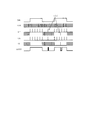
次に、本実施形態の作用について説明する。図3に示すように、分周器17を介して出力されるクロック信号CLK2(第2クロック信号)は2分周されている。ANDゲート16は、入力信号DINがハイレベルを示す期間に、クロック信号CLK2を信号DIN1として出力する(ゲート制御)。一方、ANDゲート15は、入力信号DINがローレベルを示す期間に、クロック信号CLKを信号DIN2として出力する。
Next, the operation of this embodiment will be described. As shown in FIG. 3, the clock signal CLK2 (second clock signal) output via the
パルス発生回路18(P1),19(N1)は、入力信号DINがハイレベルを示す期間に、信号DIN1の立上りエッジをトリガとしてそれぞれローレベルパルスVP1,ハイレベルパルスVN1(第1オン信号)を出力する。これらのパルスは、FET21(P1),22(N1)のゲート信号となるので、トランス11の1次側コイルL1には、両者が同時にオンしている期間に一方向,例えば正極性の電流が流れる。それに伴い、2次側コイルL2には同相の電流が誘起され、コンパレータ24Rの非反転入力端子の電位が参照電圧REF1を超えると、コンパレータ24Rはパルス状のセット信号VRを、クロック信号CLK2の周期で複数回出力する(図4参照)。これにより、RFフリップフロップ27は間欠的且つ連続的にセット状態となり、その間に、出力信号DOUTはハイレベルを示し続ける。
The pulse generation circuits 18 (P1) and 19 (N1) receive the low-level pulse VP1 and the high-level pulse VN1 (first on signal), respectively, using the rising edge of the signal DIN1 as a trigger during the period in which the input signal DIN shows a high level. Output. Since these pulses become the gate signals of the FETs 21 (P1) and 22 (N1), the primary coil L1 of the
一方、パルス発生回路18(P2),19(N2)は、入力信号DINがローレベルを示す期間に、信号DIN2の立上りエッジをトリガとしてそれぞれローレベルパルスVP2,ハイレベルパルスVN2(第2オン信号)を出力する。これらのパルスは、FET21(P2),22(N2)のゲート信号となるので、トランス11の1次側コイルL1には、両者が同時にオンしている期間に逆方向,すなわち負極性の電流が流れる。それに伴い、2次側コイルL2には同相の電流が誘起され、コンパレータ24Fの反転入力端子の電位が参照電圧REF2を下回ると、コンパレータ24Fはパルス状のリセット信号VFを、クロック信号CLK1の周期で複数回出力する(図4参照)。これにより、RFフリップフロップ27は間欠的且つ連続的にリセット状態となり、その間に、出力信号DOUTはローレベルを示し続ける。
On the other hand, the pulse generation circuits 18 (P2) and 19 (N2) are triggered by the rising edge of the signal DIN2 during the period when the input signal DIN is at the low level, respectively, and the low level pulse VP2 and the high level pulse VN2 (second on signal). ) Is output. Since these pulses become the gate signals of the FETs 21 (P2) and 22 (N2), the primary side coil L1 of the
上述した回路動作の結果として、出力信号DOUTは、図4に示すように入力信号DINと同相の信号になる。また、同図では、1次側コイルL1に流れる電流IL1を、流れる方向に応じて正負の両極性パルスで示している。 As a result of the circuit operation described above, the output signal DOUT becomes a signal in phase with the input signal DIN as shown in FIG. Further, in the figure, the current IL1 flowing through the primary coil L1 is indicated by positive and negative bipolar pulses according to the flowing direction.
ここで、同図に示すように、電流IL1に対して逆極性となるノイズパルスが印加された場合を想定する。電流IL1が負の場合に正のノイズが印加されると、それに伴い、リセット信号VFが連続して出力されている期間内にセット信号VRが出力されてRSフリップフロップ27がセットされ、出力信号DOUTはローレベルから反転してハイレベルを示す。しかし、リセット信号VFが連続して出力されているので、RSフリップフロップ27はその直後にリセットされる。したがって、出力信号DOUTは直ちにローレベルに復帰する。
Here, it is assumed that a noise pulse having a reverse polarity with respect to the current IL1 is applied as shown in FIG. When a positive noise is applied when the current IL1 is negative, the set signal VR is output and the RS flip-
また、電流IL1が正の場合に負のノイズが印加されると、それに伴い、セット信号VRが連続して出力されている期間内にリセット信号VFが出力されてRSフリップフロップ27がリセットされ、出力信号DOUTはハイレベルから反転してローレベルを示す。この場合も、セット信号VRが連続して出力されているので、RSフリップフロップ27はその直後にセットされ、出力信号DOUTは直ちにハイレベルに復帰する。
When negative current is applied when the current IL1 is positive, the reset signal VF is output during the period in which the set signal VR is continuously output, and the RS flip-
ここで、IGBT2は、ゲートに印加される信号がハイレベルの場合にオンし、ローレベルの場合にオフする。そのため、出力信号DOUTがハイレベルを示しておりIGBT2がオンしている状態でノイズの印加によりターンオフする事象よりも、出力信号DOUTがローレベルを示しており、IGBT2がオフしている状態でノイズの印加によりターンオンする事象を回避する方がより安全である、と評価できる。
Here, the
そこで本実施形態では、リセット信号VFをセット信号VRよりも速い周期で繰り返し出力することで、RSフリップフロップ27がノイズの影響によりセットされても、より速くリセット状態に復帰させるようにしている。また、対応の緊急性が低いセット信号VR側の周期を遅くすることで、信号伝達回路7の消費電力を低減する効果がある。
Therefore, in the present embodiment, the reset signal VF is repeatedly output at a cycle faster than the set signal VR, so that the reset state can be returned to the reset state more quickly even if the RS flip-
図5は、特許文献2に開示されている構成を、本実施形態の図1に相当するレベルで示したもので、クロック信号CLKを用いることなく、本実施形態の構成よりANDゲート15及び16,分周器17を削除した構成である。この構成によれば、図6に示すように、一旦逆極性のノイズが印加されると、次に正式な信号の変化エッジが入力されるまでの間、出力信号DOUTは反転したレベルを維持し続けることになる。したがって、例えば上アーム側のIGBT2Uがオフ,下アーム側のIGBT2Xがオンしている状態で、上アーム側のIGBT2Uがノイズの影響を受けてターンオンした場合には、その間に短絡電流が流れ続けることになる。そして、短絡電流が流れる状態がそのまま継続すれば、IGBT2U及び2Xが破壊に至るおそれがある。
FIG. 5 shows the configuration disclosed in
図7から図9は、入力信号DINがローレベルを示す期間に出力するパルス周期は0.5μ秒に固定し、ハイレベルを示す期間に出力するパルス周期を0.5μ秒,1.0μ秒,2.0μ秒に変化させた場合の各信号波形をシミュレーションしたものである。すると、図10に示すように、従来技術の信号伝達回路の消費電流と、本実施形態の信号伝達回路7の消費電流とを比較すると、2次側回路13の構成は同一であるから2次側の消費電流は略同一である。これに対して、信号伝達回路7は、1次側回路12がクロック信号CLKに基づくパルスを発生させるので、その分だけ消費電流が増加している。しかし、同図に示すように、入力信号DINがハイレベルを示す期間に出力するパルス信号の周期をより長くすることで、1次側の消費電流を低減できる。
FIGS. 7 to 9 show that the pulse period output during the period when the input signal DIN shows the low level is fixed to 0.5 μsec, and the pulse period output during the period when the input signal DIN shows the high level is 0.5 μsec and 1.0 μsec. , Each signal waveform is simulated when it is changed to 2.0 μsec. Then, as shown in FIG. 10, when the current consumption of the signal transmission circuit of the prior art is compared with the current consumption of the
以上のように本実施形態によれば、信号伝達回路7を構成する1次側回路12は、入力信号DINがハイレベルを示す期間に、トランス11の1次側コイルL1に一方向の電流を流すパルス信号を入力信号の変化周期よりも速い周期で発生させる。また、入力信号DINがローレベルを示す期間に、1次側コイルL1に前記方向とは逆方向の電流を流すパルス信号を、同じく入力信号DINの変化周期よりも速い周期で発生させる。そして、2次側回路13は、トランス11の2次側コイルL2に発生する極性が異なる電圧に応じてハイ及びローレベルを判別することで、入力信号を再生する。
As described above, according to the present embodiment, the
このように構成すれば、入力信号DINがハイ又はローレベルを示している期間にノイズの影響により前記レベルが反転した場合でも、2次側コイルL2には、1次側回路12が二値レベルに応じて発生させたより速い周期のパルス信号に基づく電流が繰り返し流れ、その電流に応じた極性の電圧が発生する。そして、2次側回路は13、前記電圧の極性に応じて入力信号DINを再生するので、入力信号DINが反転したレベルを短時間内に本来のレベルに復帰させる。例えば、入力信号DINがデューティ50%のPWM信号であれば、遅くともキャリア周期の1/2未満の時間内に本来のレベルに復帰できる。したがって、トランス11を用いて1次側,2次側間の電気的絶縁を図りつつ、レベルが反転したことに伴う影響を低減して、入力信号DINを用いた制御を本来の状態により早く復帰させることが可能になる。
With this configuration, even when the level is inverted due to the influence of noise during a period in which the input signal DIN indicates a high or low level, the secondary side coil L2 has a binary level of the
また、1次側回路12は、入力信号DINがハイレベルを示す期間とローレベルを示す期間とで、パルス信号を発生させる周期を変化させる。これにより、IGBT2がターンオンするハイレベルについて発生させるパルス信号の周期を相対的に速くして、入力信号DINを本来のレベルに直ちに復帰させ、IGBT2がターンオフするローレベルについて発生させるパルス信号の周期を相対的に遅くして、消費電力を低減することができる。
Further, the
そして、1次側回路12を、クロック信号CLKを分周してクロック信号CLK2を出力する分周器17,入力信号DINがハイレベルを示す期間にクロック信号CLK2を出力させるANDゲート16,ローレベルを示す期間にクロック信号CLKを出力させるNOTゲート14及びANDゲート15,各出力端子が1次側コイルL1の両端に接続されるHブリッジ回路20,ANDゲート16を介して出力されるクロック信号CLK2の立上りエッジに同期してFET21(P1)及び22(N1)にパルス信号VP1及びVN1を出力するパルス発生回路18(P1)及び19(N1),ANDゲート15を介して出力されるクロック信号CLKの立上りエッジに同期して、FET21(P2)及び22(N2)にパルス信号VP2及びVN2を出力するパルス発生回路18(P2)及び19(N2)を備えて構成した。
The
このように構成すれば、パルス信号VP1及びVN1の出力周期を、分周器17に設定する分周比に応じて変化させることができ、オンしている状態のIGBT2がノイズの影響を受けてターンオフした場合に、オン状態に復帰させる時間の速さと消費電力の削減量とを調整できる。
If comprised in this way, the output period of pulse signal VP1 and VN1 can be changed according to the frequency division ratio set to the
また、2次側回路13を、2次側コイルL2に発生する電圧が一方の極性を示す際にセット信号VRを発生させるコンパレータ24R,前記電圧が他方の極性を示す際にリセット信号VFを発生させるコンパレータ24F,セット信号VR及びリセット信号VFが入力されるRSフリップフロップ27を備えて構成した。このように構成すれば、RSフリップフロップ27は、1次側回路12がパルス信号VP1及びVN1を発生させる毎にセットされて出力信号DOUTをハイレベルにし、パルス信号VP2及びVN2を発生させる毎にリセットされて同信号をローレベルにする。したがって、2次側回路13を簡単に構成できる。
Further, the
加えて、信号伝達回路7が出力するゲート信号DOUTにより、インバータ回路1を構成するIGBT2を駆動するようにした。したがって、例えば上アームのIGBT2Uがオフ,下アームのIGBT2Xがオンしている状態でIGBT2Uがノイズの影響を受けてターンオンした場合に、IGBT2U及び2Xに短絡電流が流れる事態を短時間内に解消できる。
In addition, the
(第2実施形態)
以下、第1実施形態と同一部分には同一符号を付して説明を省略し、異なる部分についてのみ説明する。図11に示すように、第2実施形態の信号伝達回路31は、1次側回路12を1次側回路32に置き換えたもので、第1実施形態の構成より、ANDゲート16及び分周器17を削除している。そして、パルス発生回路18(P1)及び19(N1)には、入力信号DINを直接入力している。
(Second Embodiment)
Hereinafter, the same parts as those of the first embodiment are denoted by the same reference numerals, description thereof is omitted, and only different parts will be described. As shown in FIG. 11, the
次に、第2実施形態の作用について説明する。図12に示すように、入力信号DINがローレベルを示す期間に出力されるローレベルパルスVP2及びハイレベルパルスVN2は、第1実施形態と同様である。 Next, the operation of the second embodiment will be described. As shown in FIG. 12, the low-level pulse VP2 and the high-level pulse VN2 that are output during the period when the input signal DIN indicates the low level are the same as those in the first embodiment.
一方、入力信号DINがハイレベルを示す期間において、パルス発生回路18(P1),19(N1)は、入力信号DINの立上りエッジをトリガとして、それぞれローレベルパルスVP1,ハイレベルパルスVN1を1回のみ出力する。したがって、前記期間内に逆極性のノイズが印加されると、従来技術と同様に、次回に入力信号DINの立上りエッジが到来するまで、出力信号DOUTはハイレベルにはならない。このように第2実施形態では、対応の緊急性が低いセット信号VR側については、ノイズ印加時の復帰効果を付与することなく、信号伝達回路31の消費電力低減効果を最大化している。
On the other hand, during a period in which the input signal DIN is at a high level, the pulse generation circuits 18 (P1) and 19 (N1) trigger a low level pulse VP1 and a high level pulse VN1 once with the rising edge of the input signal DIN as a trigger. Output only. Accordingly, when reverse polarity noise is applied within the period, the output signal DOUT does not go high until the next rising edge of the input signal DIN arrives, as in the prior art. As described above, in the second embodiment, the power consumption reduction effect of the
以上のように第2実施形態によれば、信号伝達回路31は、第1実施形態の構成よりANDゲート16及び分周器17を削除して、1次側回路12を1次側回路32に置き換え、パルス発生回路18(P1)及び19(N1)に入力信号DINを直接入力する構成とした。これにより、IGBT2がオンしている期間の入力信号DINは1次側回路32により変調されず、その期間内にノイズの影響を受けて信号レベルが反転すると、IGBT2はターンオフして、入力信号DINが次にハイレベルを示すまでターンオンしない。したがって、消費電力を低減する効果を第1実施形態よりも向上させることができ、入力信号DINがローレベルを示す期間については第1実施形態と同様の効果が得られる。
As described above, according to the second embodiment, the
本発明は上記した、又は図面に記載した実施形態にのみ限定されるものではなく、以下のような変形又は拡張が可能である。
第1,第2レベルは何れか一方をハイレベル,他方をローレベルとすれば良い。
変化エッジは、立下りエッジでも良い。
分周器17における分周比は、「3」以上でも良い。
また、第1実施形態において、分周器17を削除しても良い。
The present invention is not limited to the embodiments described above or shown in the drawings, and the following modifications or expansions are possible.
One of the first and second levels may be a high level and the other may be a low level.
The changing edge may be a falling edge.
The frequency dividing ratio in the
Further, in the first embodiment, the
信号伝達回路を介して駆動信号を入力するスイッチング素子は、IGBTに限ることなく、MOSFETやバイポーラトランジスタなどでも良い。
必要であれば、信号伝達回路にプリドライバを加えて駆動装置を構成しても良い。
出力信号DOUTにより駆動されるスイッチング素子は、インバータ回路1を構成するものに限らず、ハーフブリッジ回路やHブリッジ回路を構成するものでも良い。また、単一のスイッチング素子を駆動対象としても良い。
スイッチング素子の駆動装置に適用するものに限ることなく、二値レベルで変化する入力信号を電気的に絶縁して伝達する必要があるものに適用が可能である。
The switching element for inputting the drive signal via the signal transmission circuit is not limited to the IGBT, but may be a MOSFET or a bipolar transistor.
If necessary, a driving device may be configured by adding a pre-driver to the signal transmission circuit.
The switching elements driven by the output signal DOUT are not limited to those constituting the
The present invention is not limited to the one applied to the driving device for the switching element, but can be applied to an input signal that needs to be electrically isolated and transmitted at a binary level.
図面中、1はインバータ回路、2はIGBT(スイッチング素子)、7は信号伝達回路(駆動装置)、11はトランス、L1は1次側コイル、L2は2次側コイル、12は1次側回路、13は2次側回路、14はNOTゲート(第2論理回路)、15はANDゲート(第2論理回路)、16はANDゲート(第1論理回路)、17は分周器、18(P1)及び19(N1)はパルス発生回路(第1オン信号出力回路)、18(P2)及び19(N2)はパルス発生回路(第2オン信号出力回路)、20はHブリッジ回路、21(P1)及び21(P2)はPチャネルMOSFET(スイッチング素子)、22(N1)及び22(N2)はNチャネルMOSFET(スイッチング素子)、24Rはコンパレータ(セット信号発生回路)、24Fはコンパレータ(リセット信号発生回路)、27はRSフリップフロップを示す。 In the drawings, 1 is an inverter circuit, 2 is an IGBT (switching element), 7 is a signal transmission circuit (drive device), 11 is a transformer, L1 is a primary coil, L2 is a secondary coil, and 12 is a primary circuit. , 13 is a secondary circuit, 14 is a NOT gate (second logic circuit), 15 is an AND gate (second logic circuit), 16 is an AND gate (first logic circuit), 17 is a frequency divider, and 18 (P1 ) And 19 (N1) are pulse generation circuits (first on signal output circuits), 18 (P2) and 19 (N2) are pulse generation circuits (second on signal output circuits), 20 is an H bridge circuit, and 21 (P1 ) And 21 (P2) are P-channel MOSFETs (switching elements), 22 (N1) and 22 (N2) are N-channel MOSFETs (switching elements), 24R is a comparator (set signal generating circuit), 24F Comparator (reset signal generating circuit), 27 denotes an RS flip-flop.
Claims (5)
二値レベルで変化する入力信号が第1レベルを示す期間に、前記トランスの1次側コイル(L1)に一方向の電流を流すパルス信号を、前記入力信号の変化周期よりも速い周期で発生させ、
前記入力信号が第2レベルを示す期間に、前記1次側コイルに前記方向とは逆方向の電流を流すパルス信号を、前記入力信号の変化周期よりも速い周期で発生させる1次側回路(12)と、
前記トランスの2次側コイル(L2)に発生する極性が異なる電圧に応じて前記第1及び第2レベルを判別することで、前記入力信号を再生する2次側回路(13)とを備え、
前記1次側回路は、前記入力信号が第1レベルを示す期間と第2レベルを示す期間とで、前記パルス信号を発生させる周期を変化させる信号伝達回路。 A transformer (11),
During the period when the input signal that changes at the binary level shows the first level, a pulse signal that causes a current in one direction to flow through the primary coil (L1) of the transformer is generated at a cycle faster than the change cycle of the input signal. Let
A primary side circuit that generates a pulse signal that causes a current in a direction opposite to the direction to flow through the primary side coil in a period that is faster than a change period of the input signal during a period in which the input signal indicates a second level. 12)
A secondary circuit (13) for regenerating the input signal by discriminating between the first and second levels according to voltages having different polarities generated in the secondary coil (L2) of the transformer ;
The primary circuit is a signal transmission circuit that changes a cycle in which the pulse signal is generated between a period in which the input signal indicates a first level and a period in which the input signal indicates a second level .
前記第1クロック信号を分周して第2クロック信号を出力する分周器(17)と、
前記入力信号が第1レベルを示す期間だけ、前記第1又は第2クロック信号の一方を出力させるようにゲート制御する第1論理回路(14及び15,16)と、
前記入力信号が第2レベルを示す期間だけ、前記第1又は第2クロック信号の他方を出力させるようにゲート制御する第2論理回路(16,14及び15)と、
各出力端子が前記1次側コイルの両端に接続されるHブリッジ回路(20)と、
前記第1論理回路を介して出力されるクロック信号の一方の変化エッジに同期して、前記Hブリッジ回路により前記1次側コイルに前記一方向の電流を流すパルス信号を発生させるため、前記Hブリッジ回路を構成するスイッチング素子(21,22)に第1オン信号を出力する第1オン信号出力回路(18(P1)−19(N1),18(P2)−19(N2))と、
前記第2論理回路を介して出力されるクロック信号の一方の変化エッジに同期して、前記Hブリッジ回路により前記1次側コイルに前記逆方向の電流を流すパルス信号を発生させるため、前記Hブリッジ回路を構成するスイッチング素子に第2オン信号を出力する第2オン信号出力回路(18(P2)−19(N2),18(P1)−19(N1))とを備えることを特徴とする請求項1記載の信号伝達回路。 The primary circuit includes an oscillation circuit that outputs a first clock signal having a period faster than a change period of the input signal;
A frequency divider (17) for dividing the first clock signal and outputting a second clock signal;
A first logic circuit (14 and 15, 16) that gates to output one of the first or second clock signals only during a period in which the input signal exhibits a first level;
A second logic circuit (16, 14, and 15) that controls the gate to output the other of the first or second clock signal only during a period in which the input signal indicates a second level;
An H-bridge circuit (20) in which each output terminal is connected to both ends of the primary coil;
The H bridge circuit generates a pulse signal that causes the current in one direction to flow through the primary coil in synchronization with one change edge of the clock signal output through the first logic circuit. A first on signal output circuit (18 (P1) -19 (N1), 18 (P2) -19 (N2)) for outputting a first on signal to the switching elements (21, 22) constituting the bridge circuit;
The H bridge circuit generates a pulse signal that causes the current in the reverse direction to flow through the primary side coil in synchronization with one change edge of the clock signal output through the second logic circuit. And a second ON signal output circuit (18 (P2) -19 (N2), 18 (P1) -19 (N1)) for outputting a second ON signal to the switching elements constituting the bridge circuit. The signal transmission circuit according to claim 1 .
二値レベルで変化する入力信号が第1レベルを示す際に、前記トランスの1次側コイル(L1)に一方向の電流を流すようにパルス信号を発生させ、
前記入力信号が第2レベルを示す期間に、前記1次側コイルに前記方向とは逆方向の電流を流すパルス信号を、前記入力信号の変化周期よりも速い周期で発生させる1次側回路(32)と、
前記トランスの2次側コイルに発生する極性が異なる電圧に応じて前記第1及び第2レベルを判別することで、前記入力信号を再生する2次側回路(13)とを備え、
前記1次側回路は、前記入力信号の変化周期よりも速い周期のクロック信号を出力する発振回路と、
前記入力信号のレベルを反転させた反転信号を出力する反転信号出力回路(14)と、
前記入力信号が第2レベルを示す期間だけ、前記クロック信号を出力させるようにゲート制御する論理回路(15)と、
各出力端子が前記1次側コイルの両端に接続されるHブリッジ回路(20)と、
前記入力信号の一方の変化エッジに同期して、前記Hブリッジ回路により前記1次側コイルに前記一方向の電流を流すパルス信号を発生させるため、前記Hブリッジ回路を構成するスイッチング素子(21,22)に第1オン信号を出力する第1オン信号出力回路(18(P1)−19(N1))と、
前記論理回路を介して出力されるクロック信号の一方の変化エッジに同期して、前記Hブリッジ回路により前記1次側コイルに前記逆方向の電流を流すパルス信号を発生させるため、前記Hブリッジ回路を構成するスイッチング素子に第2オン信号を出力する第2オン信号出力回路(18(P2)−19(N2))とを備える信号伝達回路。 A transformer (11),
When an input signal that changes at a binary level indicates the first level, a pulse signal is generated so that a one-way current flows through the primary coil (L1) of the transformer,
A primary side circuit that generates a pulse signal that causes a current in a direction opposite to the direction to flow through the primary side coil in a period that is faster than a change period of the input signal during a period in which the input signal indicates a second level. 32)
A secondary circuit (13) for regenerating the input signal by discriminating between the first and second levels according to voltages having different polarities generated in the secondary coil of the transformer ;
The primary circuit includes an oscillation circuit that outputs a clock signal having a cycle that is faster than a change cycle of the input signal;
An inverted signal output circuit (14) for outputting an inverted signal obtained by inverting the level of the input signal;
A logic circuit (15) that performs gate control so that the clock signal is output only during a period in which the input signal indicates a second level;
An H-bridge circuit (20) in which each output terminal is connected to both ends of the primary coil;
Switching elements (21, 21) constituting the H bridge circuit for generating a pulse signal for causing the primary side coil to pass the current in one direction in synchronization with one change edge of the input signal. 22) a first on signal output circuit (18 (P1) -19 (N1)) for outputting a first on signal to 22),
Since the H bridge circuit generates a pulse signal that causes the current in the reverse direction to flow through the primary coil in synchronization with one changing edge of the clock signal output through the logic circuit, the H bridge circuit A signal transmission circuit comprising a second on signal output circuit (18 (P2) -19 (N2)) for outputting a second on signal to the switching elements constituting the circuit.
前記2次側コイルに発生する電圧が他方の極性を示す際に、リセット信号を発生させるリセット信号発生回路(24F)と、
前記セット信号及び前記リセット信号が入力されるRSフリップフロップ(27)とを備える請求項1から3の何れか一項に記載の信号伝達回路。 The secondary side circuit includes a set signal generation circuit (24R) that generates a set signal when a voltage generated in the secondary side coil has one polarity;
A reset signal generating circuit (24F) for generating a reset signal when the voltage generated in the secondary coil indicates the other polarity;
The set signal and the signal transmission circuit according to any one of the RS flip-flop (27) and from 請 Motomeko 1 Ru including three said reset signal is input.
この信号伝達回路の2次側回路により再生された入力信号により、スイッチング素子(3)を駆動制御するスイッチング素子の駆動装置。 A signal transmission circuit according to any one of claims 1 to 4 , comprising:
The input signal reproduced by the secondary circuit of the signal transfer circuit, the driving device Luz switching elements to drive and control the switching element (3).
Priority Applications (5)
| Application Number | Priority Date | Filing Date | Title |
|---|---|---|---|
| JP2015083318A JP6376029B2 (en) | 2015-04-15 | 2015-04-15 | Signal transmission circuit and switching element drive device |
| US15/548,446 US20180019747A1 (en) | 2015-04-15 | 2016-03-25 | Signal transmission circuit and driving device for switching element |
| PCT/JP2016/001754 WO2016166941A1 (en) | 2015-04-15 | 2016-03-25 | Signal transmission circuit and driving for device switching element |
| CN201680017591.0A CN107431483A (en) | 2015-04-15 | 2016-03-25 | The drive device of signal transfering circuit and switch element |
| DE112016001759.6T DE112016001759T5 (en) | 2015-04-15 | 2016-03-25 | SIGNAL TRANSMISSION CIRCUIT AND CONTROL DEVICE FOR SWITCHING ELEMENT |
Applications Claiming Priority (1)
| Application Number | Priority Date | Filing Date | Title |
|---|---|---|---|
| JP2015083318A JP6376029B2 (en) | 2015-04-15 | 2015-04-15 | Signal transmission circuit and switching element drive device |
Publications (3)
| Publication Number | Publication Date |
|---|---|
| JP2016208078A JP2016208078A (en) | 2016-12-08 |
| JP2016208078A5 JP2016208078A5 (en) | 2017-06-08 |
| JP6376029B2 true JP6376029B2 (en) | 2018-08-22 |
Family
ID=57126126
Family Applications (1)
| Application Number | Title | Priority Date | Filing Date |
|---|---|---|---|
| JP2015083318A Expired - Fee Related JP6376029B2 (en) | 2015-04-15 | 2015-04-15 | Signal transmission circuit and switching element drive device |
Country Status (5)
| Country | Link |
|---|---|
| US (1) | US20180019747A1 (en) |
| JP (1) | JP6376029B2 (en) |
| CN (1) | CN107431483A (en) |
| DE (1) | DE112016001759T5 (en) |
| WO (1) | WO2016166941A1 (en) |
Families Citing this family (7)
| Publication number | Priority date | Publication date | Assignee | Title |
|---|---|---|---|---|
| GB2559423B8 (en) * | 2017-02-07 | 2023-06-28 | Heyday Integrated Circuits Sas | An isolated high side drive circuit |
| DE102018211033A1 (en) * | 2018-07-04 | 2020-01-09 | Laird Dabendorf Gmbh | Method for operating a circuit for generating an electromagnetic field and circuit |
| JP7119681B2 (en) * | 2018-07-16 | 2022-08-17 | 株式会社デンソー | Signal transmission device and drive device |
| US11495172B2 (en) | 2020-10-19 | 2022-11-08 | X Display Company Technology Limited | Pixel group and column token display architectures |
| US11488518B2 (en) | 2020-10-19 | 2022-11-01 | X Display Company Technology Limited | Pixel group and column token display architectures |
| US11430375B1 (en) | 2021-03-19 | 2022-08-30 | X Display Company Technology Limited | Pulse-density-modulation pixel control circuits and devices including them |
| US11386826B1 (en) | 2021-06-22 | 2022-07-12 | X Display Company Technology Limited | Flat-panel pixel arrays with signal regeneration |
Family Cites Families (8)
| Publication number | Priority date | Publication date | Assignee | Title |
|---|---|---|---|---|
| JP2638625B2 (en) * | 1988-09-21 | 1997-08-06 | 日本インター株式会社 | MOS-FET gate drive circuit |
| FI90605C (en) * | 1991-12-09 | 1994-02-25 | Abb Stroemberg Drives Oy | Semiconductor switch control circuit |
| JPH0715949A (en) * | 1993-06-28 | 1995-01-17 | Fuji Electric Co Ltd | Gate driving circuit for power converter |
| JP3855116B2 (en) * | 2000-03-22 | 2006-12-06 | 日本光電工業株式会社 | Semiconductor switch drive circuit |
| JP3522668B2 (en) * | 2000-08-10 | 2004-04-26 | ローム株式会社 | Signal transmission device |
| WO2011092864A1 (en) * | 2010-02-01 | 2011-08-04 | トヨタ自動車株式会社 | Signal transmission device |
| CN102832917B (en) * | 2012-08-21 | 2016-03-23 | 台达电子工业股份有限公司 | Switch driving circuit |
| CN103618437A (en) * | 2013-11-26 | 2014-03-05 | 苏州贝克微电子有限公司 | Control circuit enabling switch voltage stabilization circuit to keep high efficiency within wide current range |
-
2015
- 2015-04-15 JP JP2015083318A patent/JP6376029B2/en not_active Expired - Fee Related
-
2016
- 2016-03-25 US US15/548,446 patent/US20180019747A1/en not_active Abandoned
- 2016-03-25 WO PCT/JP2016/001754 patent/WO2016166941A1/en active Application Filing
- 2016-03-25 DE DE112016001759.6T patent/DE112016001759T5/en not_active Withdrawn
- 2016-03-25 CN CN201680017591.0A patent/CN107431483A/en active Pending
Also Published As
| Publication number | Publication date |
|---|---|
| CN107431483A (en) | 2017-12-01 |
| DE112016001759T5 (en) | 2018-01-25 |
| JP2016208078A (en) | 2016-12-08 |
| US20180019747A1 (en) | 2018-01-18 |
| WO2016166941A1 (en) | 2016-10-20 |
Similar Documents
| Publication | Publication Date | Title |
|---|---|---|
| JP6376029B2 (en) | Signal transmission circuit and switching element drive device | |
| TW543275B (en) | Brushless motor drive circuit having low noise and high efficiency | |
| TW200845033A (en) | Semiconductor device | |
| JP2007013916A (en) | Signal generator | |
| TWI482432B (en) | Quasi-shift circuit | |
| JP2016208078A5 (en) | ||
| US8994437B2 (en) | Semiconductor device and circuit for controlling potential of gate of insulated gate type switching device | |
| US20130194006A1 (en) | Dead time generation circuit and load driving apparatus | |
| JP2011062021A (en) | Dead time generating circuit and motor control device | |
| JP6354937B2 (en) | Drive circuit, integrated circuit device, and charge pump circuit control method | |
| US10581351B2 (en) | Method to reduce the commutation loss in a motor inverter | |
| TWI683541B (en) | Level shift circuit | |
| JP6009833B2 (en) | Power converter | |
| JP2012019645A5 (en) | ||
| JP2022093787A (en) | Motor driver device | |
| JP6399019B2 (en) | Gate voltage control device | |
| JP4470616B2 (en) | Bidirectional switch drive power supply circuit | |
| JP6277691B2 (en) | Control signal generation circuit and circuit device | |
| JP7207990B2 (en) | mask circuit | |
| JP6291947B2 (en) | Drive circuit, integrated circuit device, and charge pump circuit control method | |
| JP2013169030A (en) | Switching element control circuit and switching element control method | |
| JP2017153332A (en) | Motor control device | |
| JP2016119773A (en) | Power conversion device | |
| JP2013051843A (en) | Half bridge circuit | |
| JP2018148729A (en) | Power conversion apparatus |
Legal Events
| Date | Code | Title | Description |
|---|---|---|---|
| A521 | Request for written amendment filed |
Free format text: JAPANESE INTERMEDIATE CODE: A523 Effective date: 20170421 |
|
| A621 | Written request for application examination |
Free format text: JAPANESE INTERMEDIATE CODE: A621 Effective date: 20170421 |
|
| TRDD | Decision of grant or rejection written | ||
| A01 | Written decision to grant a patent or to grant a registration (utility model) |
Free format text: JAPANESE INTERMEDIATE CODE: A01 Effective date: 20180626 |
|
| A61 | First payment of annual fees (during grant procedure) |
Free format text: JAPANESE INTERMEDIATE CODE: A61 Effective date: 20180709 |
|
| R151 | Written notification of patent or utility model registration |
Ref document number: 6376029 Country of ref document: JP Free format text: JAPANESE INTERMEDIATE CODE: R151 |
|
| LAPS | Cancellation because of no payment of annual fees |