JP6361171B2 - Equivalent circuit - Google Patents
Equivalent circuit Download PDFInfo
- Publication number
- JP6361171B2 JP6361171B2 JP2014042726A JP2014042726A JP6361171B2 JP 6361171 B2 JP6361171 B2 JP 6361171B2 JP 2014042726 A JP2014042726 A JP 2014042726A JP 2014042726 A JP2014042726 A JP 2014042726A JP 6361171 B2 JP6361171 B2 JP 6361171B2
- Authority
- JP
- Japan
- Prior art keywords
- circuit
- internal electrode
- terminal
- inductance
- equivalent circuit
- Prior art date
- Legal status (The legal status is an assumption and is not a legal conclusion. Google has not performed a legal analysis and makes no representation as to the accuracy of the status listed.)
- Active
Links
Images
Description
本発明は、積層型コンデンサのシミュレーション用の等価回路に関する。 The present invention relates to an equivalent circuit for simulation of a multilayer capacitor.
この種の分野の従来技術として、例えば特許文献1に記載されたものが知られている。特許文献1に記載の積層チップコンデンサの等価回路モデルでは、基本等価回路の等価直列キャパシタンスと等価直列レジスタンスの一部を、スタティックキャパシタンスと、積層チップコンデンサ内における内部電極の角や端の近くに発生する電磁場分布の異常特性に関する回路素子として、キャパシタンス及びレジスタンスを設けている。このような構成により、この等価回路モデルでは、実際の回路性能との誤差の発生の抑制を図っている。
As a prior art in this type of field, for example, one described in
上記のように、等価回路では、実製品の積層型コンデンサの特性との誤差を抑制し、実製品の積層型コンデンサの特性に近似する特性を得ることが求められている。 As described above, the equivalent circuit is required to suppress the difference from the characteristics of the actual multilayer capacitor and to obtain characteristics that approximate the characteristics of the actual multilayer capacitor.
本発明は、実製品の積層型コンデンサの特性に近似する特性を得ることができる等価回路を提供することを目的とする。 An object of the present invention is to provide an equivalent circuit capable of obtaining characteristics approximating those of an actual multilayer capacitor.
本発明に係る等価回路は、積層型コンデンサのシミュレーション用の等価回路であって、積層型コンデンサの内部電極を示す第1回路部と、積層型コンデンサの静電容量を示す第2回路部と、を有し、第1回路部は、3つ以上設けられており、その少なくとも2つ以上においてインダクタンス成分を有しており、第2回路部は、一の第1回路部と他の第1回路部との間に接続されており、第1回路部のインダクタンス成分の間に相互インダクタンスが設定されていることを特徴とする。 An equivalent circuit according to the present invention is an equivalent circuit for simulating a multilayer capacitor, and includes a first circuit portion indicating an internal electrode of the multilayer capacitor, a second circuit portion indicating a capacitance of the multilayer capacitor, There are three or more first circuit parts, and at least two of the first circuit parts have inductance components, and the second circuit part includes one first circuit part and another first circuit. And a mutual inductance is set between the inductance components of the first circuit unit.
この等価回路は、内部電極を示す第1回路部が3つ以上設けられている。このように、等価回路では、第1回路部を3つ以上設けることにより、ある所定の周波数において内部共振現象が生じる。このとき、各第1回路部には、通常よりも大きい電流(共振電流)が流れることになる。共振電流が損失を有する第1回路部に流れると、等価回路全体のインピーダンス特性において損失のピークとして現れる。このピークは、実製品の積層型コンデンサにおいて発生する。したがって、等価回路では、実製品の積層型コンデンサの特性に近づけることができる。また、等価回路では、インダクタンス成分の間に相互インダクタンスが設定されている。これにより、等価回路では、実製品の積層コンデンサにおいて生じる物理現象(内部電極間の電流のアンバランスや内部電極間で生じる共振現象)が実現可能となる。したがって、等価回路では、実製品の積層型コンデンサの特性に近似する特性を得ることができる。 This equivalent circuit is provided with three or more first circuit portions indicating internal electrodes. Thus, in the equivalent circuit, by providing three or more first circuit portions, an internal resonance phenomenon occurs at a predetermined frequency. At this time, a current (resonant current) larger than usual flows through each first circuit unit. When the resonance current flows through the first circuit portion having a loss, it appears as a loss peak in the impedance characteristics of the entire equivalent circuit. This peak occurs in an actual multilayer capacitor. Therefore, the equivalent circuit can be close to the characteristics of the actual multilayer capacitor. In the equivalent circuit, a mutual inductance is set between the inductance components. Thereby, in the equivalent circuit, a physical phenomenon (an imbalance of current between the internal electrodes or a resonance phenomenon generated between the internal electrodes) that occurs in the actual multilayer capacitor can be realized. Therefore, in the equivalent circuit, it is possible to obtain characteristics that approximate the characteristics of the actual multilayer capacitor.
一実施形態においては、第1回路部は抵抗成分を有し、抵抗成分は、直列に接続された複数のインダクタンス素子と、各インダクタンス素子それぞれの両端部に対して一端が接続され、互いに並列に接続された複数の抵抗素子と、を有していてもよい。このように第1回路部の抵抗成分をインダクタンス素子及び抵抗素子により構成することにより、表皮効果を考慮することが可能となり、高周波帯域における抵抗成分(ESR:等価直列抵抗)が大きくなる。したがって、実製品の積層型コンデンサの特性に更に近似する特性を得ることができる。 In one embodiment, the first circuit unit has a resistance component, and the resistance component has a plurality of inductance elements connected in series and one end connected to each end of each inductance element, and in parallel with each other. And a plurality of connected resistance elements. Thus, by configuring the resistance component of the first circuit portion with an inductance element and a resistance element, it is possible to consider the skin effect, and the resistance component (ESR: equivalent series resistance) in the high frequency band is increased. Therefore, it is possible to obtain characteristics that further approximate the characteristics of the actual multilayer capacitor.
一実施形態においては、第2回路部は、第1容量素子と、第2容量素子と抵抗素子とが直列に接続された直列回路と、を有し、直列回路は、1以上設けられており、第1容量素子と直列回路とが並列に接続されていてもよい。このように第2回路部を第1容量素子と直列回路とにより構成することにより、誘電損失を考慮することが可能となり、低周波側における静電容量の成分を大きく且つ抵抗成分を小さくできる。したがって、実製品の積層型コンデンサの特性に更に近似する特性を得ることができる。 In one embodiment, the second circuit unit includes a first capacitor element and a series circuit in which the second capacitor element and the resistor element are connected in series, and one or more series circuits are provided. The first capacitor element and the series circuit may be connected in parallel. By configuring the second circuit portion with the first capacitive element and the series circuit in this way, it is possible to consider dielectric loss, and the capacitance component on the low frequency side can be increased and the resistance component can be decreased. Therefore, it is possible to obtain characteristics that further approximate the characteristics of the actual multilayer capacitor.
一実施形態においては、第1〜第4の端子を有し、第1端子及び3端子は、第1回路部により電気的に接続されており、第2端子及び4端子は、第1端子及び第3端子に接続された第1回路部とは異なる第1回路部により電気的に接続されていてもよい。このような構成により、等価回路は、貫通コンデンサとして構成されている。ここで、貫通型コンデンサでは、4つの端子電極のうち、内部電極で電気的に接続された第2端子電極及び第4端子電極をグランドに接続すると、内部電極では、第2端子電極と第4端子電極とに向かって、同じ大きさで互いに逆方向のノイズ電流が流れる。このとき、第2端子電極に向かう電流により生じる磁束と、第4端子電極に向かう電流により生じる磁束とは、互いに打ち消し合う。これにより、貫通型コンデンサでは、ESL(等価直列インダクタンス)を低減することができる。等価回路は、貫通型コンデンサの構成をモデル化しており、インダクタンス成分間において相互インダクタンスを設定している。これにより、等価回路では、貫通型コンデンサと同等の特性を得ることができ、貫通型コンデンサにおける磁束の打ち消しの効果のモデル化を図れる。 In one embodiment, it has the 1st-the 4th terminal, the 1st terminal and 3 terminals are electrically connected by the 1st circuit part, and the 2nd terminal and 4 terminals are the 1st terminal and The first circuit unit that is different from the first circuit unit connected to the third terminal may be electrically connected. With this configuration, the equivalent circuit is configured as a feedthrough capacitor. Here, in the feedthrough capacitor, when the second terminal electrode and the fourth terminal electrode electrically connected by the internal electrode among the four terminal electrodes are connected to the ground, the second terminal electrode and the fourth terminal electrode are connected to the ground. Noise currents of the same size and in opposite directions flow toward the terminal electrodes. At this time, the magnetic flux generated by the current flowing toward the second terminal electrode and the magnetic flux generated by the current flowing toward the fourth terminal electrode cancel each other. Thereby, in the feedthrough capacitor, ESL (equivalent series inductance) can be reduced. The equivalent circuit models the structure of the feedthrough capacitor and sets the mutual inductance between the inductance components. Thereby, in the equivalent circuit, characteristics equivalent to those of the feedthrough capacitor can be obtained, and the effect of canceling the magnetic flux in the feedthrough capacitor can be modeled.
本発明によれば、実製品の積層型コンデンサの特性に近似する特性を得ることができる。 According to the present invention, it is possible to obtain characteristics that approximate the characteristics of the actual multilayer capacitor.
以下、添付図面を参照して、本発明の好適な実施形態について詳細に説明する。なお、図面の説明において同一又は相当要素には同一符号を付し、重複する説明は省略する。 Hereinafter, preferred embodiments of the present invention will be described in detail with reference to the accompanying drawings. In the description of the drawings, the same or equivalent elements will be denoted by the same reference numerals, and redundant description will be omitted.
[第1実施形態]
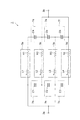
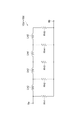
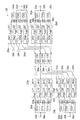
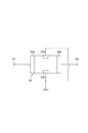
図1は、第1実施形態に係る等価回路を示す図である。図1に示す等価回路1は、例えば、電子部品を用いた回路設計や分析のシミュレーションに用いられる回路であり、コンピュータにおいて実行される回路設計(分析)プログラムに適用される。
[First Embodiment]
FIG. 1 is a diagram illustrating an equivalent circuit according to the first embodiment. An
図1に示すように、等価回路1は、第1端子3a及び第2端子3bと、内部電極部(第1回路部)5a〜5dと、静電容量部(第2回路部)7a〜7fと、を備えている。図1に示す等価回路1は、図2に示すように、誘電体層101が積層されてなる素体102と、素体102内に配置された2層の第1内部電極104a,104c及び2層の第2内部電極104b,104dと、第1内部電極104a,104cに接続された第1端子電極106aと、第2内部電極104b,104dに接続された第2端子電極106bと、を備える積層型コンデンサ100の等価回路である。第1内部電極104a,104cと第2内部電極104b,104dとは、交互に配置されている。第1端子3aは、第1端子電極106aに相当し、第2端子3bは、第2端子電極106bに相当する。内部電極部5a〜5dは、第1内部電極104a,104c及び第2内部電極104b,104dに相当する。
As shown in FIG. 1, the
内部電極部5a〜5dは、積層型コンデンサ100の内部電極104a〜104dを示している。内部電極部5a〜5dは、4つ設けられている。これは、積層型コンデンサ100において、内部電極104a〜104dが4層配置されていることを示している。内部電極部5a,5cは、第1端子3aに接続されている。つまり、内部電極部5a,5cは、第1内部電極104a,104cに相当する。内部電極部5b,5dは、第2端子3bに接続されている。つまり、内部電極部5b,5dは、第2内部電極104b,104dに相当する。
The
内部電極部5aは、インダクタンス素子(インダクタンス成分)L1と、抵抗素子R1と、を有している。インダクタンス素子L1と抵抗素子R1とは、直列に接続されており、RL直列回路を構成している。インダクタンス素子L1は、内部電極や接続導体などによる寄生インダクタンスを表している。抵抗素子R1は、内部電極や接続導体などの導体損失を表している。
The
内部電極部5bは、インダクタンス素子L2と、抵抗素子R2と、を有している。内部電極部5cは、インダクタンス素子L3と、抵抗素子R3と、を有している。内部電極部5dは、インダクタンス素子L4と、抵抗素子R4と、を有している。
The
静電容量部7a〜7fは、積層型コンデンサ100の静電容量を示している。静電容量部7a〜7fは、内部電極部5a〜5dの間に配置されている。具体的には、内部電極部5aと内部電極部5bとの間には、静電容量部7aと静電容量部7dとが配置されている。すなわち、静電容量部7a,7dは、内部電極部5a,5bにより発生する静電容量を表している。
同様に、内部電極部5bと内部電極部5cとの間には、静電容量部7bと静電容量部7eとが配置されている。すなわち、静電容量部7b,7eは、内部電極部5b,5cにより発生する静電容量を表している。内部電極部5cと内部電極部5dとの間には、静電容量部7cと静電容量部7fとが配置されている。すなわち、静電容量部7c,7fは、内部電極部5c,5dにより発生する静電容量を表している。各静電容量部7a〜7fは、キャパシタンス素子C1,C2,C3,C4,C5,C6をそれぞれ有している。
Similarly, the
本実施形態では、内部電極部5a〜5dにおいて、インダクタンス素子L1〜L4間に相互インダクタンスが設定されている。詳細には、インダクタンス素子L1とインダクタンス素子L2との結合係数K1、インダクタンス素子L1とインダクタンス素子L3との結合係数K2、インダクタンス素子L1とインダクタンス素子L4との結合係数K3、インダクタンス素子L2とインダクタンス素子L3との結合係数K4、インダクタンス素子L2とインダクタンス素子L4との結合係数K5、及び、インダクタンス素子L3とインダクタンス素子L4との結合係数K6が設定されている。各結合係数K1〜K6は、実製品の積層型コンデンサの特性に応じて適宜設定される。
In the present embodiment, mutual inductance is set between the inductance elements L1 to L4 in the
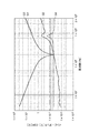
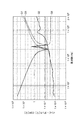
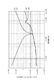
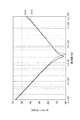
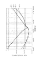
図3は、図1に示す等価回路におけるインピーダンス及びESRの周波数特性のシミュレーション結果を示す図である。図4は、比較例の等価回路におけるインピーダンス及びESRの周波数特性のシミュレーション結果を示す図である。図3及び図4では、縦軸はインピーダンス[Ω]、ESR(等価直列抵抗)[Ω]を示し、横軸は周波数[Hz]を示している。また、図3及び図4では、実製品の積層型コンデンサのインピーダンスの実測値をG1、ESRの実測値をG2で示し、本実施形態の等価回路1におけるインピーダンスをG3,G5、ESRをG4,G6で示している。
FIG. 3 is a diagram showing a simulation result of frequency characteristics of impedance and ESR in the equivalent circuit shown in FIG. FIG. 4 is a diagram showing simulation results of impedance and ESR frequency characteristics in the equivalent circuit of the comparative example. 3 and 4, the vertical axis represents impedance [Ω] and ESR (equivalent series resistance) [Ω], and the horizontal axis represents frequency [Hz]. 3 and 4, the measured impedance value of the actual multilayer capacitor is indicated by G1, the measured value of ESR is indicated by G2, the impedance in the
図3に示すように、実製品の積層型コンデンサでは、グラフG1で示されるように、周波数が200MHz付近でインピーダンスが極小値となっている。これは、コンデンサの静電容量によるリアクタンスと等価直列インダクタンスによるインダクタンスとが打ち消し合い、合計のリアクタンス値がゼロになるためである。また、実製品の積層型コンデンサでは、グラフG2で示されるように、周波数が800MHz付近でESRのピークが発生している。これは、内部共振によるものである。これに対して、等価回路1では、グラフG3で示されるように、周波数が200MHz付近でインピーダンスが極小値となっており、グラフG4で示されるように、周波数800MHz付近でESRのピークが発生している。つまり、等価回路1では、実製品の積層型コンデンサの実測値と略同等の特性を得ることができる。
As shown in FIG. 3, the actual multilayer capacitor has a minimum impedance at a frequency of around 200 MHz, as shown by a graph G1. This is because the reactance due to the capacitance of the capacitor and the inductance due to the equivalent series inductance cancel each other, and the total reactance value becomes zero. In the actual multilayer capacitor, as shown in the graph G2, an ESR peak occurs at a frequency near 800 MHz. This is due to internal resonance. On the other hand, in the
一方、図4に示すように、インダクタンス素子L1〜L4間において相互インダクタンスを設定していない(結合係数K1〜K6を0に設定した)回路では、グラフG5,G6で示されるように、実製品の積層型コンデンサの特性(グラフG1,G2)とは異なる特性を示している。比較例の等価回路では、実製品の積層型コンデンサで生じる内部共振現象が適切に再現されないため、実製品の積層型コンデンサとは異なる特性を示している。したがって、等価回路1のインダクタンス素子L1〜L4間において相互インダクタンス(結合係数K1〜K6)を設定することの有効性が確認された。
On the other hand, as shown in FIG. 4, in a circuit in which mutual inductance is not set between the inductance elements L1 to L4 (coupling coefficients K1 to K6 are set to 0), as shown in graphs G5 and G6, the actual product This shows characteristics different from those of the multilayer capacitor (graphs G1 and G2). In the equivalent circuit of the comparative example, the internal resonance phenomenon that occurs in the actual multilayer capacitor is not properly reproduced, and thus exhibits different characteristics from the actual multilayer capacitor. Therefore, the effectiveness of setting the mutual inductance (coupling coefficients K1 to K6) between the inductance elements L1 to L4 of the
以上説明したように、本実施形態に係る等価回路1は、内部電極部5a〜5dを備えている。このように、等価回路1では、内部電極部(内部電極)を3以上(本実施形態では4個)備えることにより、ある所定の周波数において内部共振現象が生じる。このとき、各内部電極部5a〜5dには、通常よりも大きい電流(共振電流)が流れることになる。共振電流が損失を有する内部電極に流れると、等価回路1全体のインピーダンス特性において損失のピークとして現れる。したがって、図2に示すように、等価回路1では、実製品の積層型コンデンサの特性に近づけることができる。
As described above, the
また、本実施形態の等価回路1では、インダクタンス素子L1〜L4の間に相互インダクタンスが設定されている。これにより、等価回路1では、実製品の積層コンデンサにおいて生じる物理現象(内部電極間の電流のアンバランスや内部電極間で生じる共振現象)が実現可能となる。したがって、等価回路1では、実製品の積層型コンデンサの特性に近似する特性を得ることができる。
In the
[第2実施形態]
続いて、第2実施形態について説明する。第2実施形態に係る等価回路は、内部電極部5a〜5dの抵抗素子R1〜R4に替えて抵抗部(抵抗成分)10a〜10dを備える点で第1実施形態と異なっている。図5は、第2実施形態に係る等価回路における内部電極部の抵抗部の構成を示す回路図である。
[Second Embodiment]
Next, the second embodiment will be described. The equivalent circuit according to the second embodiment is different from the first embodiment in that it includes resistance portions (resistance components) 10a to 10d instead of the resistance elements R1 to R4 of the
図5に示すように、抵抗部(抵抗成分)10aは、インダクタンス素子Lh2〜Lh5と、抵抗素子Rh1〜Rh5と、を備えている。インダクタンス素子Lh2,Lh3,Lh4,Lh5は、この順番に直列に接続されている。インダクタンス素子Lh2の一端は、端子9aに接続されている。本実施形態では、インダクタンス素子Lh2〜Lh5を4個、抵抗素子Rh1〜Rh5を5個用いているが、インダクタンス素子及び抵抗素子の数は、設計に応じて適宜設定されればよい。 As shown in FIG. 5, the resistance portion (resistance component) 10 a includes inductance elements Lh2 to Lh5 and resistance elements Rh1 to Rh5. The inductance elements Lh2, Lh3, Lh4, and Lh5 are connected in series in this order. One end of the inductance element Lh2 is connected to the terminal 9a. In this embodiment, four inductance elements Lh2 to Lh5 and five resistance elements Rh1 to Rh5 are used. However, the number of inductance elements and resistance elements may be appropriately set according to the design.
抵抗素子Rh1は、その一端がインダクタンス素子Lh2の一端(端子9a)に接続され、その他端が端子9bに接続されている。抵抗素子Rh2は、その一端がインダクタンス素子Lh2の他端で且つインダクタンス素子Lh3の一端に接続され、その他端が端子9bに接続されている。すなわち、インダクタンス素子Lh2の両端部に対して、抵抗素子Rh1及び抵抗素子Rh2の一端が接続されている。抵抗素子Rh3は、その一端がインダクタンス素子Lh3の他端で且つインダクタンス素子Lh4の一端に接続され、その他端が端子9bに接続されている。抵抗素子Rh4は、その一端がインダクタンス素子Lh4の他端で且つインダクタンス素子Lh5の一端に接続され、その他端が端子9bに接続されている。抵抗素子Rh5は、その一端がインダクタンス素子Lh5の他端に接続され、その他端が端子9bに接続されている。2つのインダクタンス素子と1つの抵抗素子は、T型回路を構成している。抵抗部10b〜10dについても、抵抗部10aと同様の構成を有している。
One end of the resistance element Rh1 is connected to one end (terminal 9a) of the inductance element Lh2, and the other end is connected to the terminal 9b. The resistor element Rh2 has one end connected to the other end of the inductance element Lh2 and one end of the inductance element Lh3, and the other end connected to the terminal 9b. That is, one end of the resistance element Rh1 and the resistance element Rh2 is connected to both ends of the inductance element Lh2. The resistance element Rh3 has one end connected to the other end of the inductance element Lh3 and one end of the inductance element Lh4, and the other end connected to the terminal 9b. The resistance element Rh4 has one end connected to the other end of the inductance element Lh4 and one end of the inductance element Lh5, and the other end connected to the terminal 9b. The resistor element Rh5 has one end connected to the other end of the inductance element Lh5 and the other end connected to the terminal 9b. Two inductance elements and one resistance element form a T-type circuit. The resistance portions 10b to 10d also have the same configuration as that of the
図6は、図5に示す抵抗部を備えた等価回路におけるインピーダンス及びESRの周波数特性のシミュレーション結果を示す図である。図6では、縦軸はインピーダンス[Ω]、ESR(等価直列抵抗)[Ω]を示し、横軸は周波数[Hz]を示している。図6では、実製品の積層型コンデンサのインピーダンスの実測値をG1、ESRの実測値をG2で示し、本実施形態の等価回路におけるインピーダンスをG7、ESRをG8で示している。 FIG. 6 is a diagram illustrating a simulation result of the impedance and ESR frequency characteristics in the equivalent circuit including the resistance unit illustrated in FIG. 5. In FIG. 6, the vertical axis represents impedance [Ω] and ESR (equivalent series resistance) [Ω], and the horizontal axis represents frequency [Hz]. In FIG. 6, the measured impedance value of the actual multilayer capacitor is indicated by G1, the measured value of ESR is indicated by G2, the impedance in the equivalent circuit of this embodiment is indicated by G7, and the ESR is indicated by G8.
図6に示すように、内部電極部5a〜5dにおいて抵抗部10a〜10dを備える等価回路では、グラフG7,G8で示されるように、周波数が1GHz以下の帯域において、実製品の積層型コンデンサの実測値(グラフG1,G2)と略同等の特性を得られており、周波数800MHz付近で生じるESRのピークもモデル化が図られている。周波数が1GHz以上の帯域において実測値と差異が生じている点について、実製品の積層型コンデンサでは、多数の内部電極が設けられており、内部電極間において高次の共振が生じている。本実施形態の等価回路では、内部電極部5a〜5dにより4層の内部電極を備えた構成となっているため、1次共振のみがモデル化されている。そのため、本実施形態の等価回路において内部電極部の数を増やすことにより、周波数が1GHz以上の帯域においても実測値に近づけることが可能となる。
As shown in FIG. 6, in the equivalent circuit including the
以上説明したように、第2実施形態に係る等価回路では、抵抗部10a〜10dは、直列に接続されたインダクタンス素子Lh2〜Lh5と、抵抗素子Rh1〜Rh5とから構成されている。実製品の積層型コンデンサでは、高周波になるほど、表皮効果により導体の抵抗が増加する。本実施形態では、内部電極で生じる損失をより詳細に実現するために、抵抗部10a〜10dを、インダクタンス素子Lh2〜Lh5及び抵抗素子Rh1〜Rh5により構成している。これにより、表皮効果を考慮した等価回路を構成できる。したがって、高周波における抵抗成分が大きくなり、実製品の積層型コンデンサの特性に更に近似させることができる。
As described above, in the equivalent circuit according to the second embodiment, the
[第3実施形態]
続いて、第3実施形態について説明する。第3実施形態に係る等価回路は、静電容量部7a〜7fのキャパシタンス素子C1〜C6に替えて静電容量回路12a〜12fを備える点で第1実施形態と異なっている。この等価回路において、内部電極部5a〜5dの構成は、第2実施形態と同様である。すなわち、内部電極部5a〜5dは、抵抗部10a〜10dを備えている。図7は、第3実施形態に係る等価回路の静電容量部の静電容量回路の構成を示す回路図である。
[Third Embodiment]
Subsequently, the third embodiment will be described. The equivalent circuit according to the third embodiment is different from the first embodiment in that
図7に示すように、静電容量回路12a〜12fは、キャパシタンス素子(第1容量素子)Cf1と、CR直列回路14a〜14eと、を備えている。CR直列回路14aは、キャパシタンス素子(第2容量素子)Cf2と、抵抗素子Rf2とが直列に接続されている。同様に、CR直列回路14b〜14eは、キャパシタンス素子Cf3〜Cf6と、抵抗素子Rf3〜Rf6とが直列に接続されている。CR直列回路14a〜14eは、1以上設けられており、本実施形態では、5個設けられている。CR直列回路の数は、設計に応じて適宜設定されればよい。
As shown in FIG. 7, the
キャパシタンス素子Cf1とCR直列回路14a〜14eとは、並列に接続されている。詳細には、キャパシタンス素子Cf1は、その一端が端子15aに接続され、その他端が端子15bに接続されている。CR直列回路14aは、キャパシタンス素子Cf2の一端が端子15aに接続され、抵抗素子Rf2の他端が端子15bに接続されている。CR直列回路14b〜14eについても同様である。
The capacitance element Cf1 and the
図8は、図7に示す静電容量回路を備えた等価回路におけるインピーダンス及びESRの周波数特性のシミュレーション結果を示す図である。図8では、縦軸はインピーダンス[Ω]、ESR(等価直列抵抗)[Ω]を示し、横軸は周波数[Hz]を示している。図8では、実製品の積層型コンデンサのインピーダンスの実測値をG9、ESRの実測値をG10で示し、本実施形態の等価回路におけるインピーダンスをG11、ESRをG12で示している。 FIG. 8 is a diagram illustrating simulation results of impedance and ESR frequency characteristics in an equivalent circuit including the capacitance circuit illustrated in FIG. In FIG. 8, the vertical axis represents impedance [Ω] and ESR (equivalent series resistance) [Ω], and the horizontal axis represents frequency [Hz]. In FIG. 8, the measured impedance value of the actual multilayer capacitor is indicated by G9, the measured value of ESR is indicated by G10, the impedance in the equivalent circuit of this embodiment is indicated by G11, and the ESR is indicated by G12.
図8に示すように、静電容量回路12a〜12fを備える等価回路では、グラフG11,G12で示されるように、周波数が1GHzの以下の帯域において、実製品の積層型コンデンサの実測値(グラフG9,G10)と略同等の特性を得られている。実測値では、20MHz付近においてESRのピークが発生しているが、この等価回路においても、20MHz付近においてESRのピークが発生している。また、周波数が1MHz以下の帯域において、実製品の積層型コンデンサでは、誘電損失によりESRが周波数に反比例する特性を有しているが、この等価回路においても、実製品の積層型コンデンサと同様の特性が得られている。
As shown in FIG. 8, in the equivalent circuit including the
以上説明したように、第3実施形態に係る等価回路では、静電容量部7a〜7fの静電容量回路12a〜12fは、キャパシタンス素子Cf1とCR直列回路14a〜14eとが並列に接続された構成を有している。このように静電容量回路12a〜12fを構成することにより、誘電損失を考慮することが可能となり、低周波側における静電容量の成分を大きく且つ抵抗成分を小さくできる。また、この等価回路では、内部電極で生じる損失をより詳細に実現するために、抵抗部10a〜10dを設けている。したがって、この等価回路では、内部電極において生じる表皮効果による損失と、誘電体によって生じる誘電体損の影響を考慮しているため、実製品の積層コンデンサの特性をより詳細にモデル化することができる。
As described above, in the equivalent circuit according to the third embodiment, the
[第4実施形態]
続いて、第4実施形態について説明する。図9は、第4実施形態に係る等価回路を示す図である。図9に示すように、等価回路20は、第1端子22a、第2端子22b、第3端子22c及び第4端子22dと、内部電極部23a〜23d、内部電極部24a〜24d、内部電極部26a〜26d及び内部電極部28a〜28dと、静電容量部29a〜29c、静電容量部30a〜30c、静電容量部32a〜32c、静電容量部34a〜34c及び静電容量部36a〜36cと、を備えている。
[Fourth Embodiment]
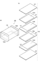
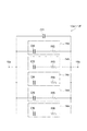
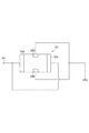
Subsequently, a fourth embodiment will be described. FIG. 9 is a diagram illustrating an equivalent circuit according to the fourth embodiment. As shown in FIG. 9, the
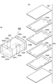
図9に示す等価回路20は、図10に示すように、誘電体層201が積層されていると共に直方体形状を成し、長手方向で対向する一対の端面202a,202b、幅方向で対向する一対の側面202c,202d及び高さ方向で対向する一対の主面202e,202fを有する素体202と、素体202内に配置された第1〜第4内部電極204a〜204dと、第1内部電極204a及び第3内部電極204cに接続され且つ素体202の端面202a,202bにそれぞれ配置された第1端子電極206a及び第3端子電極206cと、第2内部電極204b及び第4内部電極204dに接続され且つ素体202の側面202c,202dにそれぞれ配置された第2端子電極206b及び第4端子電極206dと、を備える貫通型コンデンサ200の等価回路である。第1端子22aは、第1端子電極206aに相当し、第2端子22bは、第2端子電極206bに相当する。第3端子22cは、第3端子電極206cに相当し、第4端子22dは、第4端子電極206dに相当する。
As shown in FIG. 10, the
この貫通型コンデンサ200では、第1端子電極206a及び第3端子電極206cが第1内部電極204a及び第3内部電極204cを介して導通しており、第2端子電極206b及び第4端子電極206dが第2内部電極204b及び第4内部電極204dを介して導通しており、第1端子電極206a及び第3端子電極206cと第2端子電極206b及び第4端子電極206dとの間にて静電容量を有している。貫通型コンデンサ200は、第1端子電極206aと第3端子電極206cとの間に信号を通し、第2端子電極206bと第4端子電極206dを回路のグランドに接続して使用される。これにより、貫通型コンデンサ200では、第1端子電極206aと第3端子電極206cを通過する信号成分に含まれる高周波ノイズが第2端子電極206b及び第4端子電極206dを介してグランドに流れるため、第1端子電極206a及び第3端子電極206cを通過する高周波ノイズを除去できる。
In the
内部電極部23a〜23d、内部電極部24a〜24d、内部電極部26a〜26d及び内部電極部28a〜28dは、貫通型コンデンサ200の内部電極204a〜204dを示している。内部電極部23a〜23d、内部電極部24a〜24d、内部電極部26a〜26d及び内部電極部28a〜28dは、それぞれ4つ設けられている。これは、貫通型コンデンサ200において、内部電極204a〜204dが4層配置されていることを示している。
The
内部電極部23a、内部電極部24a、内部電極部26a及び内部電極部28aは、第1内部電極204aに相当する。内部電極部23a及び内部電極部26aは、第1端子22a及び第3端子22cに接続されている。内部電極部23b、内部電極部24b、内部電極部26b及び内部電極部28bは、第2内部電極204bに相当する。内部電極部24b及び内部電極部28bは、第2端子22b及び第4端子22dに接続されている。
The
内部電極部23c、内部電極部24c、内部電極部26c及び内部電極部28cは、第3内部電極204cに相当する。内部電極部23c及び内部電極部26cは、第1端子22a及び第3端子22cに接続されている。内部電極部23d、内部電極部24d、内部電極部26d及び内部電極部28dは、第4内部電極204dに相当する。内部電極部24d及び内部電極部28dは、第2端子22b及び第4端子22dに接続されている。
The
内部電極部23aは、インダクタンス素子L11と、抵抗部R11と、を有している。インダクタンス素子L11と抵抗部R11とは、直列に接続されており、RL直列回路を構成している。内部電極部23bは、インダクタンス素子L12と、抵抗部R12と、を有している。内部電極部23cは、インダクタンス素子L13と、抵抗部R13と、を有している。内部電極部23dは、インダクタンス素子L14と、抵抗部R14と、を有している。
The
内部電極部24aは、インダクタンス素子L21と、抵抗部R21と、を有している。インダクタンス素子L21と抵抗部R21とは、直列に接続されており、RL直列回路を構成している。内部電極部24bは、インダクタンス素子L22と、抵抗部R22と、を有している。内部電極部24cは、インダクタンス素子L23と、抵抗部R23と、を有している。内部電極部24dは、インダクタンス素子L24と、抵抗部R24と、を有している。
The
内部電極部26aは、インダクタンス素子L31と、抵抗部R31と、を有している。インダクタンス素子L31と抵抗部R31とは、直列に接続されており、RL直列回路を構成している。内部電極部26bは、インダクタンス素子L32と、抵抗部R32と、を有している。内部電極部26cは、インダクタンス素子L33と、抵抗部R33と、を有している。内部電極部26dは、インダクタンス素子L34と、抵抗部R34と、を有している。
The
内部電極部28aは、インダクタンス素子L41と、抵抗部R41と、を有している。インダクタンス素子L41と抵抗部R41とは、直列に接続されており、RL直列回路を構成している。内部電極部28bは、インダクタンス素子L42と、抵抗部R42と、を有している。内部電極部28cは、インダクタンス素子L43と、抵抗部R43と、を有している。内部電極部28dは、インダクタンス素子L44と、抵抗部R44と、を有している。
The
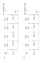
図11(a)に示すように、抵抗部R11〜R14,R31〜R34のそれぞれは、抵抗素子Rh11〜Rh15と、インダクタンス素子Lh12〜Lh15と、を備えている。インダクタンス素子Lh12,Lh13,Lh14,Lh15は、この順番に直列に接続されている。インダクタンス素子Lh12の一端は、端子40aに接続されている。 As shown to Fig.11 (a), each of resistance part R11-R14, R31-R34 is provided with resistance element Rh11-Rh15 and inductance element Lh12-Lh15. The inductance elements Lh12, Lh13, Lh14, and Lh15 are connected in series in this order. One end of the inductance element Lh12 is connected to the terminal 40a.
抵抗素子Rh11は、その一端がインダクタンス素子Lh12の一端(端子40a)に接続され、その他端が端子40bに接続されている。抵抗素子Rh12は、その一端がインダクタンス素子Lh12の他端で且つインダクタンス素子Lh13の一端に接続され、その他端が端子40bに接続されている。抵抗素子Rh13は、その一端がインダクタンス素子Lh13の他端で且つインダクタンス素子Lh14の一端に接続され、その他端が端子40bに接続されている。抵抗素子Rh14は、その一端がインダクタンス素子Lh14の他端で且つインダクタンス素子Lh15の一端に接続され、その他端が端子40bに接続されている。抵抗素子Rh15は、その一端がインダクタンス素子Lh15の他端に接続され、その他端が端子40bに接続されている。2つのインダクタンス素子と1つの抵抗素子は、T型回路を構成している。 One end of the resistance element Rh11 is connected to one end (terminal 40a) of the inductance element Lh12, and the other end is connected to the terminal 40b. The resistance element Rh12 has one end connected to the other end of the inductance element Lh12 and one end of the inductance element Lh13, and the other end connected to the terminal 40b. The resistor element Rh13 has one end connected to the other end of the inductance element Lh13 and one end of the inductance element Lh14, and the other end connected to the terminal 40b. The resistance element Rh14 has one end connected to the other end of the inductance element Lh14 and one end of the inductance element Lh15, and the other end connected to the terminal 40b. The resistor element Rh15 has one end connected to the other end of the inductance element Lh15 and the other end connected to the terminal 40b. Two inductance elements and one resistance element form a T-type circuit.
図11(b)に示すように、抵抗部R21〜R24,R41〜R44は、抵抗素子Rh21〜Rh25と、インダクタンス素子Lh22〜Lh25と、を備えている。インダクタンス素子Lh22,Lh23,Lh24,Lh25は、この順番に直列に接続されている。インダクタンス素子Lh22の一端は、端子42aに接続されている。 As shown in FIG. 11B, the resistance portions R21 to R24, R41 to R44 include resistance elements Rh21 to Rh25 and inductance elements Lh22 to Lh25. The inductance elements Lh22, Lh23, Lh24, and Lh25 are connected in series in this order. One end of the inductance element Lh22 is connected to the terminal 42a.
抵抗素子Rh21は、その一端がインダクタンス素子Lh22の一端(端子42a)に接続され、その他端が端子42bに接続されている。抵抗素子Rh22は、その一端がインダクタンス素子Lh22の他端で且つインダクタンス素子Lh23の一端に接続され、その他端が端子42bに接続されている。抵抗素子Rh23は、その一端がインダクタンス素子Lh23の他端で且つインダクタンス素子Lh24の一端に接続され、その他端が端子42bに接続されている。抵抗素子Rh24は、その一端がインダクタンス素子Lh24の他端で且つインダクタンス素子Lh25の一端に接続され、その他端が端子42bに接続されている。抵抗素子Rh25は、その一端がインダクタンス素子Lh25の他端に接続され、その他端が端子42bに接続されている。2つのインダクタンス素子と1つの抵抗素子は、T型回路を構成している。 One end of the resistance element Rh21 is connected to one end (terminal 42a) of the inductance element Lh22, and the other end is connected to the terminal 42b. The resistance element Rh22 has one end connected to the other end of the inductance element Lh22 and one end of the inductance element Lh23, and the other end connected to the terminal 42b. The resistor element Rh23 has one end connected to the other end of the inductance element Lh23 and one end of the inductance element Lh24, and the other end connected to the terminal 42b. The resistance element Rh24 has one end connected to the other end of the inductance element Lh24 and one end of the inductance element Lh25, and the other end connected to the terminal 42b. The resistance element Rh25 has one end connected to the other end of the inductance element Lh25 and the other end connected to the terminal 42b. Two inductance elements and one resistance element form a T-type circuit.
ここで、貫通型コンデンサ200の内部電極204a〜204dは、長方形形状を呈している。そのため、内部電極204a〜204dの長手方向と幅方向とでは、回路パラメータが異なる。本実施形態では、内部電極部23a〜23d及び内部電極部26a〜26dは、内部電極の長手方向(横方向)に対する回路パラメータである。内部電極部24a〜24d及び内部電極部28a〜28dは、内部電極の幅方向(縦方向)に対する回路パラメータである。
Here, the
静電容量部29a〜29c、静電容量部30a〜30c、静電容量部32a〜32c、静電容量部34a〜34c及び静電容量部36a〜36cは、貫通型コンデンサの静電容量を示している。静電容量部29a、静電容量部30a、静電容量部32a、静電容量部34a及び静電容量部36aは、第1内部電極と第2内部電極との静電容量を示している。静電容量部29b、静電容量部30b、静電容量部32b、静電容量部34b及び静電容量部36bは、第2内部電極と第3内部電極との静電容量を示している。静電容量部29c、静電容量部30c、静電容量部32c、静電容量部34c及び静電容量部36cは、第3内部電極と第4内部電極との静電容量を示している。
各静電容量部29a〜29cは、静電容量回路C11,C12,C13をそれぞれ有している。各静電容量部30a〜30cは、静電容量回路C21,C22,C23をそれぞれ有している。各静電容量部32a〜32cは、静電容量回路C31,C32,C33をそれぞれ有している。各静電容量部34a〜34cは、静電容量回路C41,C42,C43をそれぞれ有している。各静電容量部36a〜36cは、静電容量回路C51,C52,C53をそれぞれ有している。
Each of the
静電容量回路C11〜C13、静電容量回路C21〜C23、静電容量回路C31〜C33、静電容量回路C41〜C43及び静電容量回路C51〜53は、図7に示す静電容量回路12aと同様の構成を有している。すなわち、静電容量回路C11〜C13、静電容量回路C21〜C23、静電容量回路C31〜C33、静電容量回路C41〜C43及び静電容量回路C51〜53のそれぞれは、キャパシタンス素子Cf1と、CR直列回路14a〜14eと、を備えている。CR直列回路14aは、キャパシタンス素子Cf2と、抵抗素子Rf2とが直列に接続されている。同様に、CR直列回路14b〜14eは、キャパシタンス素子Cf3〜Cf6と、抵抗素子Rf3〜Rf6とが直列に接続されている。
The capacitance circuits C11 to C13, the capacitance circuits C21 to C23, the capacitance circuits C31 to C33, the capacitance circuits C41 to C43, and the capacitance circuits C51 to C53 are the
本実施形態では、内部電極部23a〜23d及び内部電極部26a〜26dにおいて、インダクタンス素子L11〜L14及びL31〜L34間に相互インダクタンスが設定されている。内部電極部24a〜24d及び内部電極部28a〜28dにおいて、インダクタンス素子L21〜L24及びL41〜L44間に相互インダクタンスが設定されている。各インダクタンス素子間の結合係数は、実製品の貫通型コンデンサの特性に応じて適宜設定される。
In the present embodiment, mutual inductance is set between the inductance elements L11 to L14 and L31 to L34 in the
図12は、図9に示す等価回路におけるSパラメータの周波数特性のシミュレーション結果を示す図である。図12では、縦軸はSパラメータ[dB]を示し、横軸は周波数[Hz]を示している。図12では、実製品の貫通型コンデンサのSパラメータの実測値をG13で示し、本実施形態の等価回路20におけるSパラメータをG14で示している。
FIG. 12 is a diagram showing a simulation result of the frequency characteristics of the S parameter in the equivalent circuit shown in FIG. In FIG. 12, the vertical axis indicates the S parameter [dB], and the horizontal axis indicates the frequency [Hz]. In FIG. 12, the measured value of the S parameter of the actual feedthrough capacitor is indicated by G13, and the S parameter in the
ここで、Sパラメータの測定方法について説明する。図13は、Sパラメータの測定回路を示す図である。図13では、等価回路20を貫通型コンデンサに適用した場合について示している。図13に示すように、貫通型コンデンサのSパラメータを測定する場合には、第1端子22aをポートP1に接続し、第3端子22cをポートP2に接続する。第2端子22b及び第4端子22dは、グランドに接続する。Sパラメータとして、ポートP1からポートP2への伝送特性S21を測定した。結果を図12に示す。
Here, a method for measuring the S parameter will be described. FIG. 13 is a diagram illustrating an S parameter measurement circuit. FIG. 13 shows a case where the
図12に示すように、等価回路20では、グラフG14に示されるように、極小値において実製品の貫通型コンデンサ(グラフG13)と多少の差異はあるものの、実製品の貫通型コンデンサと近似する伝送特性が得られている。
As shown in FIG. 12, in the
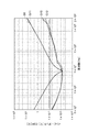
図14は、図9に示す等価回路におけるインピーダンス及びESRの周波数特性のシミュレーション結果を示す図である。図14では、縦軸はインピーダンス[Ω]、ESR[Ω]を示し、横軸は周波数[Hz]を示している。図14では、実製品の貫通型コンデンサのインピーダンスの実測値をG15、ESRの実測値をG16で示し、本実施形態の等価回路20におけるインピーダンスをG17、ESRをG18で示している。
FIG. 14 is a diagram illustrating simulation results of impedance and ESR frequency characteristics in the equivalent circuit illustrated in FIG. 9. In FIG. 14, the vertical axis indicates impedance [Ω] and ESR [Ω], and the horizontal axis indicates frequency [Hz]. In FIG. 14, the measured value of the impedance of the actual feedthrough capacitor is indicated by G15, the measured value of ESR is indicated by G16, the impedance in the
ここで、貫通型コンデンサのインピーダンス及びESR特性の測定方法について説明する。図15は、インピーダンス及びESRの測定回路を示す図である。図15では、等価回路20を貫通型コンデンサに適用した場合について示している。図15に示すように、インピーダンス及びESRを測定する場合には、第1端子22a及び第3端子22cを測定端子mcに接続し、第2端子22b及び第4端子22dをグランドに接続する。測定端子mcとグランドとの間のインピーダンス及びESRを測定した。
Here, a method for measuring the impedance and ESR characteristics of the feedthrough capacitor will be described. FIG. 15 is a diagram showing a measurement circuit for impedance and ESR. FIG. 15 shows a case where the
図14に示すように、等価回路20では、グラフG17,G18で示されるように、1GHz以下の周波数帯域において、実製品の貫通型コンデンサの実測値(グラフG15,G16)に近似する特性を得られている。
As shown in FIG. 14, in the
以上説明したように、本実施形態に係る等価回路20は、貫通型コンデンサ200の構成を有している。貫通型コンデンサ200では、第2端子電極206b及び第4端子電極206dをグランドに接続すると、第2端子電極206b及び第4端子電極206dに接続された第2内部電極204b及び第4内部電極204dでは、第2端子電極206bと第4端子電極206dとに向かって、同じ大きさで互いに逆方向のノイズ電流が流れる。このとき、第2端子電極206bに向かう電流により生じる磁束と、第4端子電極206dに向かう電流により生じる磁束とは、互いに打ち消し合う。これにより、貫通型コンデンサ200では、ESL(等価直列インダクタンス)を低減することができる。本実施形態に係る等価回路20は、貫通型コンデンサ200の構成をモデル化しており、インダクタンス素子L11〜L14,L21〜L24,L31〜L34,L41〜L44間において相互インダクタンスを設定している。これにより、等価回路20では、貫通型コンデンサ200と同等の特性を得ることができ、貫通型コンデンサ200における磁束の打ち消しの効果のモデル化を図れる。
As described above, the
本発明は、上記実施形態に限定されるものではない。例えば、上記実施形態では、4層の内部電極を有する積層型コンデンサ(貫通型コンデンサ)の構成を一例に説明したが、内部電極の数は設計に応じて適宜設定されればよい。 The present invention is not limited to the above embodiment. For example, in the above-described embodiment, the configuration of a multilayer capacitor (through-type capacitor) having four layers of internal electrodes has been described as an example, but the number of internal electrodes may be set as appropriate according to the design.
1,20…等価回路、5a〜5d,23a〜23d,24a〜24d,26a〜26d,28a〜28d…内部電極部(第1回路部)、7a〜7f,29a〜29c,30a〜30c,32a〜32c,34a〜34c,36a〜36c…静電容量部(第2回路部)、10a〜10d,R11〜R14,R21〜R24,R31〜R34,R41〜R44…抵抗部(抵抗成分)、14a〜14e…CR直列回路(直列回路)、22a〜22d…第1〜第4端子、Cf1…キャパシタンス素子(第1容量素子)、Cf2〜Cf6…キャパシタンス素子(第2容量素子)、L1〜L4,L11〜L14,L21〜L24,L31〜L34,L41〜L44…インダクタンス素子(インダクタンス成分)、Lh2〜Lh5,Lh12〜Lh15,Lh22〜Lh25…インダクタンス素子、Rh1〜Rh5,Rh11〜Rh15,Rh21〜Rh25…抵抗素子。
DESCRIPTION OF
Claims (5)
前記プログラムに設定されている前記等価回路は、
前記積層型コンデンサの内部電極を示す第1回路部と、
前記積層型コンデンサの静電容量を示す第2回路部と、を有し、
前記第1回路部は、3つ以上設けられており、その少なくとも2つ以上においてインダクタンス成分を有しており、
前記第2回路部は、一の前記第1回路部と他の前記第1回路部との間に接続されており、
前記第1回路部の前記インダクタンス成分の間に相互インダクタンスが設定されるように、前記等価回路が作成されており、
前記等価回路を用いてシミュレーションを行うことを特徴とするシミュレーション方法。 A method in which a computer executes a program in which an equivalent circuit for simulation of a multilayer capacitor is set, and performs simulation .
The equivalent circuit set in the program is
A first circuit portion showing an internal electrode of the multilayer capacitor;
A second circuit portion showing a capacitance of the multilayer capacitor,
Three or more of the first circuit portions are provided, and at least two of the first circuit portions have inductance components,
The second circuit unit is connected between one first circuit unit and the other first circuit unit,
Wherein the so that set mutual inductance between the inductance component of the first circuit portion, said equivalent circuit being created,
A simulation method comprising performing a simulation using the equivalent circuit .
前記抵抗成分は、
直列に接続された複数のインダクタンス素子と、
各前記インダクタンス素子それぞれの両端部に対して一端が接続され、互いに並列に接続された複数の抵抗素子と、を有することを特徴とする請求項1記載のシミュレーション方法。 The first circuit unit has a resistance component;
The resistance component is
A plurality of inductance elements connected in series;
The simulation method according to claim 1, further comprising: a plurality of resistance elements connected at one end to each end of each of the inductance elements and connected in parallel to each other.
第1容量素子と、
第2容量素子と抵抗素子とが直列に接続された直列回路と、を有し、
前記直列回路は、1以上設けられており、
前記第1容量素子と前記直列回路とが並列に接続されていることを特徴とする請求項1又は2記載のシミュレーション方法。 The second circuit unit includes:
A first capacitive element;
A series circuit in which a second capacitance element and a resistance element are connected in series,
One or more series circuits are provided,
The simulation method according to claim 1, wherein the first capacitor element and the series circuit are connected in parallel.
前記第1端子及び前記3端子は、前記第1回路部により電気的に接続されており、
前記第2端子及び前記4端子は、前記第1端子及び前記第3端子に接続された前記第1回路部とは異なる前記第1回路部により電気的に接続されていることを特徴とする請求項1〜3のいずれか一項記載のシミュレーション方法。 The equivalent circuit has first to fourth terminals,
The first terminal and the three terminals are electrically connected by the first circuit unit,
The second terminal and the four terminals are electrically connected by the first circuit unit different from the first circuit unit connected to the first terminal and the third terminal. The simulation method according to any one of Items 1 to 3.
前記等価回路は、The equivalent circuit is
前記積層型コンデンサの内部電極を示す第1回路部と、A first circuit portion showing an internal electrode of the multilayer capacitor;
前記積層型コンデンサの静電容量を示す第2回路部と、を有し、A second circuit portion showing a capacitance of the multilayer capacitor,
前記第1回路部は、3つ以上設けられており、その少なくとも2つ以上においてインダクタンス成分を有するように設定されており、Three or more first circuit portions are provided, and at least two of the first circuit portions are set to have an inductance component,
前記第2回路部は、一の前記第1回路部と他の前記第1回路部との間に接続されるように設定されており、The second circuit unit is set to be connected between one first circuit unit and the other first circuit unit,
前記第1回路部の前記インダクタンス成分の間に相互インダクタンスが設定されるように、前記等価回路が作成されていることを特徴とするプログラム。The program, wherein the equivalent circuit is created so that a mutual inductance is set between the inductance components of the first circuit unit.
Priority Applications (1)
| Application Number | Priority Date | Filing Date | Title |
|---|---|---|---|
| JP2014042726A JP6361171B2 (en) | 2014-03-05 | 2014-03-05 | Equivalent circuit |
Applications Claiming Priority (1)
| Application Number | Priority Date | Filing Date | Title |
|---|---|---|---|
| JP2014042726A JP6361171B2 (en) | 2014-03-05 | 2014-03-05 | Equivalent circuit |
Publications (2)
| Publication Number | Publication Date |
|---|---|
| JP2015170004A JP2015170004A (en) | 2015-09-28 |
| JP6361171B2 true JP6361171B2 (en) | 2018-07-25 |
Family
ID=54202724
Family Applications (1)
| Application Number | Title | Priority Date | Filing Date |
|---|---|---|---|
| JP2014042726A Active JP6361171B2 (en) | 2014-03-05 | 2014-03-05 | Equivalent circuit |
Country Status (1)
| Country | Link |
|---|---|
| JP (1) | JP6361171B2 (en) |
Families Citing this family (2)
| Publication number | Priority date | Publication date | Assignee | Title |
|---|---|---|---|---|
| CN110703213B (en) * | 2019-10-09 | 2021-12-21 | 中国舰船研究设计中心 | Radar interference environment equivalent physical simulation method and device |
| JP7276284B2 (en) * | 2020-08-27 | 2023-05-18 | 株式会社村田製作所 | Multilayer Capacitor Simulation Model Generation Method and Multilayer Capacitor Simulation Method |
Family Cites Families (3)
| Publication number | Priority date | Publication date | Assignee | Title |
|---|---|---|---|---|
| JP4507421B2 (en) * | 2001-02-27 | 2010-07-21 | パナソニック株式会社 | Passive element equivalent circuit model derivation method, simulator, and storage medium |
| JP5573868B2 (en) * | 2012-03-07 | 2014-08-20 | 株式会社村田製作所 | Equivalent circuit creation method, equivalent circuit creation program, and equivalent circuit creation device |
| JP2013228997A (en) * | 2012-03-30 | 2013-11-07 | Taiyo Yuden Co Ltd | Characteristic simulation method and device of circuit including multilayer chip varistor, and analysis method for circuit constant of equivalent circuit |
-
2014
- 2014-03-05 JP JP2014042726A patent/JP6361171B2/en active Active
Also Published As
| Publication number | Publication date |
|---|---|
| JP2015170004A (en) | 2015-09-28 |
Similar Documents
| Publication | Publication Date | Title |
|---|---|---|
| CN107017856B (en) | Band-pass filter and branching filter | |
| JP5652542B2 (en) | Directional coupler | |
| TWI508440B (en) | Band-pass filter | |
| TWI729327B (en) | Multilayer band pass filter | |
| KR101968585B1 (en) | Differential and common mode filter | |
| KR20140146764A (en) | Power divider | |
| JP6504182B2 (en) | Electronic parts | |
| JP6361171B2 (en) | Equivalent circuit | |
| WO2011147470A1 (en) | Electrical double filter structure and its multi -layer implementation | |
| JP6729839B2 (en) | Coil component and filter circuit including the same | |
| US9882541B2 (en) | Electronic component | |
| JP2822825B2 (en) | Composite electronic components | |
| JP2016144115A (en) | Common mode filter | |
| JP5725158B2 (en) | Electronic components | |
| WO2023179089A1 (en) | Resonator, filter, and multiplexer | |
| JP6907680B2 (en) | Low pass filter | |
| US10110192B2 (en) | Electronic component | |
| KR101441343B1 (en) | Electrical filter structure | |
| WO2016170708A1 (en) | Circuit board and filter circuit using same | |
| JPWO2017017987A1 (en) | Circuit board, filter circuit using the same, and capacitance element | |
| JP4453462B2 (en) | Noise filter | |
| WO2021149583A1 (en) | Band-pass filter | |
| JPH04273608A (en) | Electromagnetic interference filter | |
| JP6471995B2 (en) | Common mode filter | |
| TWM531695U (en) | Low pass filter with broadband suppression |
Legal Events
| Date | Code | Title | Description |
|---|---|---|---|
| A621 | Written request for application examination |
Free format text: JAPANESE INTERMEDIATE CODE: A621 Effective date: 20161121 |
|
| A977 | Report on retrieval |
Free format text: JAPANESE INTERMEDIATE CODE: A971007 Effective date: 20171110 |
|
| A131 | Notification of reasons for refusal |
Free format text: JAPANESE INTERMEDIATE CODE: A131 Effective date: 20171121 |
|
| A521 | Written amendment |
Free format text: JAPANESE INTERMEDIATE CODE: A523 Effective date: 20180118 |
|
| TRDD | Decision of grant or rejection written | ||
| A01 | Written decision to grant a patent or to grant a registration (utility model) |
Free format text: JAPANESE INTERMEDIATE CODE: A01 Effective date: 20180529 |
|
| A61 | First payment of annual fees (during grant procedure) |
Free format text: JAPANESE INTERMEDIATE CODE: A61 Effective date: 20180611 |
|
| R150 | Certificate of patent or registration of utility model |
Ref document number: 6361171 Country of ref document: JP Free format text: JAPANESE INTERMEDIATE CODE: R150 |