JP6355397B2 - SOLID-STATE IMAGING ELEMENT CONTROL METHOD, ELECTRONIC DEVICE, PROGRAM, STORAGE MEDIUM - Google Patents
SOLID-STATE IMAGING ELEMENT CONTROL METHOD, ELECTRONIC DEVICE, PROGRAM, STORAGE MEDIUM Download PDFInfo
- Publication number
- JP6355397B2 JP6355397B2 JP2014081439A JP2014081439A JP6355397B2 JP 6355397 B2 JP6355397 B2 JP 6355397B2 JP 2014081439 A JP2014081439 A JP 2014081439A JP 2014081439 A JP2014081439 A JP 2014081439A JP 6355397 B2 JP6355397 B2 JP 6355397B2
- Authority
- JP
- Japan
- Prior art keywords
- signal
- clock
- unit
- period
- state
- Prior art date
- Legal status (The legal status is an assumption and is not a legal conclusion. Google has not performed a legal analysis and makes no representation as to the accuracy of the status listed.)
- Active
Links
Images


Classifications
-
- H—ELECTRICITY
- H04—ELECTRIC COMMUNICATION TECHNIQUE
- H04N—PICTORIAL COMMUNICATION, e.g. TELEVISION
- H04N25/00—Circuitry of solid-state image sensors [SSIS]; Control thereof
- H04N25/70—SSIS architectures; Circuits associated therewith
- H04N25/76—Addressed sensors, e.g. MOS or CMOS sensors
- H04N25/78—Readout circuits for addressed sensors, e.g. output amplifiers or A/D converters
-
- H—ELECTRICITY
- H04—ELECTRIC COMMUNICATION TECHNIQUE
- H04N—PICTORIAL COMMUNICATION, e.g. TELEVISION
- H04N25/00—Circuitry of solid-state image sensors [SSIS]; Control thereof
- H04N25/70—SSIS architectures; Circuits associated therewith
- H04N25/76—Addressed sensors, e.g. MOS or CMOS sensors
- H04N25/7795—Circuitry for generating timing or clock signals
Landscapes
- Engineering & Computer Science (AREA)
- Multimedia (AREA)
- Signal Processing (AREA)
- Transforming Light Signals Into Electric Signals (AREA)
Description
本発明は、固体撮像素子及びそれを備えた電子機器に関するものである。 The present invention relates to a solid-state imaging device and an electronic apparatus including the same.
近年、撮像素子等のように、アナログ処理部と、ロジックやメモリ等のデジタル処理部とを一つのチップに混載する様にデバイス化した素子が考案されている。例えば、アナログ処理部とデジタル処理部とを別々の半導体層で形成したものを、ウェハーレベル、またはチップレベルで積層化することで、夫々の集積度を損なうことなく、1チップ化するものである。 2. Description of the Related Art In recent years, there has been devised an element in which an analog processing unit and a digital processing unit such as a logic or a memory are mounted on a single chip, such as an image sensor. For example, an analog processing unit and a digital processing unit formed by separate semiconductor layers are stacked at a wafer level or a chip level, so that one chip is obtained without impairing the degree of integration. .
図13は、CMOSイメージセンサー等の従来の撮像素子80の要部ブロック図である。画素信号を取得するための駆動制御は駆動タイミング生成部81で行われ、駆動タイミング生成部81からの駆動信号を受けて、画素アレイ82において光電変換した電荷を電位として取得する。画素アレイ82から得た電圧レベルは、A/D変換部84でデジタル化される。A/D変換部84は、A/D変換部制御部83によって制御される。
FIG. 13 is a principal block diagram of a
図14は、図13の撮像素子のアナログ信号処理部とデジタル信号処理部とを積層した場合の夫々の半導体層での受け持ちを示した、積層構成による撮像素子の要部ブロック図である。図14において、第1の層90はアナログ処理部を含む層であり、第2の層96はデジタル処理部を含む層である。
FIG. 14 is a block diagram of a main part of an image pickup device having a stacked structure, showing the handling of each semiconductor layer when the analog signal processing unit and the digital signal processing unit of the image pickup device of FIG. 13 are stacked. In FIG. 14, a
図14のブロック91, 92, 93, 94は、図13のブロック81, 82, 83, 84と夫々等価である。但し、A/D変換部94及び制御部93は、第2の層96側に搭載される例を示している。また、図14のブロック95には、第2の層96側にデジタル要素として搭載されるロジックやメモリが実装される。
図14の第1の層90及び第2の層96は、前述の様に積層化されるが、この半導体層同士の接近は、互いの層の動作により発生する電磁波の影響や、発熱による影響を生じさせる。この様な問題の解決のために、特許文献1では、積層間の貫通電極が形成される領域を除く領域に金属層を形成し、シールド層としての役割を与えている。
The
しかしながら、異なる半導体層での信号間接続には安定した共通の電位(グランド:以下、GNDと記載)の設定が必要であるが、局所的なGNDの接続ではGND間のインピーダンスが無視出来ない。そのため、電流が流れる動作毎に各層のGND間に電位を持ち、それがダイナミックに変動することになる。 However, the connection between signals in different semiconductor layers requires a stable common potential (ground: hereinafter referred to as GND), but the impedance between GND cannot be ignored in the local GND connection. For this reason, every operation in which current flows, there is a potential between the GNDs of each layer, which dynamically changes.
また、デジタル層側で特定のクロックを基準に動作する同期回路設計を採用した場合には、クロックのエッジ(立ち上がり・立ち下がり)毎に同期した状態保持素子(フリップフロップ回路:以下、FF素子と記載)の状態の切り替えが行われる。それにより、同時に大量のFF素子によって電流が消費される。FF素子出力につながるコンビネーションロジック(AND素子・OR素子等からなる組合せ回路)で消費する電流も同様のタイミングで流れる。 In addition, when a synchronous circuit design that operates based on a specific clock on the digital layer side is adopted, a state holding element (flip-flop circuit: hereinafter referred to as FF element) synchronized at each clock edge (rising / falling) State) is switched. Thereby, current is simultaneously consumed by a large amount of FF elements. The current consumed by the combination logic (combination circuit composed of AND elements, OR elements, etc.) connected to the FF element output also flows at the same timing.
デジタル層側の同一タイミングでの電流消費は、デジタル側GNDの電位を持ち上げ、見かけ上の電源変動として影響を及ぼす。その結果、前述の積層化したアナログ処理部からの信号電位をA/D変換してデジタル信号を取得する際に、アナログ信号の取得電位の変動やA/D変換器で使用するリファレンス電位の変動を生ずる。その結果、最終的にはデジタル処理に起因した周期ノイズとなって画質の低下を招く。 Current consumption at the same timing on the digital layer side raises the potential on the digital side GND, and has an effect as an apparent power supply fluctuation. As a result, when the digital signal is acquired by A / D converting the signal potential from the above-described stacked analog processing unit, the fluctuation of the acquisition potential of the analog signal and the fluctuation of the reference potential used in the A / D converter Is produced. As a result, the image quality eventually deteriorates due to periodic noise caused by digital processing.
本発明は上述した課題に鑑みてなされたものであり、その目的は、アナログ信号処理部とデジタル信号処理部を積層して構成される撮像素子において、ノイズによる画質の低下を抑制することである。 The present invention has been made in view of the above-described problems, and an object of the present invention is to suppress deterioration in image quality due to noise in an imaging device configured by stacking an analog signal processing unit and a digital signal processing unit. .
本発明に係わる固体撮像素子は、撮像画素部を有し、アナログ信号処理を主に受け持つ第1の半導体層と、デジタル信号処理を受け持つ第2の半導体層とを有する積層型の固体撮像素子であって、前記撮像画素部の駆動タイミングを生成する第1のタイミング制御手段と、前記撮像画素部の出力であるアナログ信号をデジタル信号に変換するA/D変換器と、前記A/D変換器の駆動のタイミング信号を生成する第2のタイミング制御手段と、前記第2の半導体層のデジタル信号処理部の同期回路を動作させるためのクロックを生成するクロック生成手段と、前記画素部における電荷に基づく信号を読み出す期間または前記A/D変換器において前記信号をA/D変換している期間において、前記第1および第2のタイミング制御手段の少なくともどちらかが生成するイベントタイミングを受け取って、前記第2の半導体層に実装されたデジタル信号処理部の動作を制限するために、前記クロックをマスクするマスク信号を生成する状態生成手段と、を備え、前記クロック生成手段の出力するクロックは、前記状態生成手段から出力されたマスク信号によってクロックエッジを一定期間、又は間欠的にマスクすることで前記デジタル信号処理部の動作期間の制御を行うことを特徴とする。
また、本発明に係わる固体撮像素子は、撮像画素部と該撮像画素部を駆動する駆動制御部とを有する第1の半導体層と、前記撮像画素部の出力であるアナログ信号をデジタル信号に変換するA/D変換器と前記デジタル信号を処理する信号処理部とを有する第2の半導体層とを備える積層型の固体撮像素子であって、前記駆動制御部と前記信号処理部を動作させるためのクロックを生成する生成手段と、前記撮像画素部における電荷に基づく信号を読み出す期間または前記A/D変換器において前記信号をA/D変換している期間において、前記生成手段が生成するクロックに基づいて前記信号処理の動作を制限する制限手段と、を備え、前記生成手段の出力するクロックは、前記制限手段から出力されたマスク信号によってクロックエッジを一定期間、又は間欠的にマスクすることで前記信号処理部の動作期間の制御を行うことを特徴とする。
A solid-state imaging device according to the present invention is a stacked solid-state imaging device having an imaging pixel unit and having a first semiconductor layer mainly responsible for analog signal processing and a second semiconductor layer responsible for digital signal processing. A first timing control unit that generates drive timing of the imaging pixel unit; an A / D converter that converts an analog signal output from the imaging pixel unit into a digital signal; and the A / D converter. Second timing control means for generating a driving timing signal, clock generating means for generating a clock for operating a synchronizing circuit of the digital signal processing section of the second semiconductor layer, and charge in the pixel section the signal in the period in which a / D conversion in a period or the a / D converter reads the based signals, little of the first and second timing control means Receiving an event timing of generating either also has a, in order to limit the operation of the digital signal processing unit that is mounted on the second semiconductor layer, and the state generating means for generating a mask signal for masking the clock, the The clock output from the clock generation means controls the operation period of the digital signal processing unit by masking a clock edge for a certain period or intermittently by a mask signal output from the state generation means. It is characterized by.
The solid-state imaging device according to the present invention converts a first semiconductor layer having an imaging pixel unit and a drive control unit that drives the imaging pixel unit, and an analog signal output from the imaging pixel unit into a digital signal. A solid-state imaging device including a second semiconductor layer having an A / D converter that performs processing and a signal processing unit that processes the digital signal, in order to operate the drive control unit and the signal processing unit Generating means for generating the clock of the imaging pixel section , and a clock generated by the generating means during a period of reading out a signal based on charges in the imaging pixel unit or a period of A / D conversion of the signal in the A / D converter. based and a restricting means for restricting the operation of the signal processing, the output clock of said generating means, clock edge by the mask signal output from the limiting means A certain period, or and performs intermittent control of the operation period of the signal processing unit by masking.
本発明によれば、アナログ信号処理部とデジタル信号処理部を積層して構成される撮像素子において、ノイズによる画質の低下を抑制することが可能となる。 ADVANTAGE OF THE INVENTION According to this invention, in the image pick-up element comprised by laminating | stacking an analog signal processing part and a digital signal processing part, it becomes possible to suppress the fall of the image quality by noise.
以下、本発明の実施形態について、添付図面を参照して詳細に説明する。 Hereinafter, embodiments of the present invention will be described in detail with reference to the accompanying drawings.
(第1の実施形態)
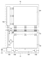
本実施形態は、固体撮像素子の構造に関する。本実施形態における撮像素子を実現する半導体素子は、撮像素子部等のアナログ信号処理部を実装した第1の層とデジタル回路部を実装した第2の層との積層構造を有する。図1は、本実施形態における撮像素子の構成を示すブロック図であり、第1の層10には撮像素子部が実装されており、第2の層11にはデジタル回路部が実装されている。
(First embodiment)
The present embodiment relates to the structure of a solid-state image sensor. A semiconductor element that realizes an image sensor in the present embodiment has a stacked structure of a first layer on which an analog signal processing unit such as an image sensor unit is mounted and a second layer on which a digital circuit unit is mounted. FIG. 1 is a block diagram illustrating a configuration of an image sensor according to the present embodiment. An image sensor unit is mounted on the
図1において、センサーアレイ部101は、光電変換部とトランジスタを含む1画素分の撮像部を二次元のアレイ構成として有する。駆動制御部102は、センサーアレイ部101を駆動するための回路である。本実施形態では、駆動制御部102で取扱う撮像画素部駆動信号(後述する図3における信号sig_301,sig_302,sig_303)の動作に起因したデジタル側回路の動作の制御(クロックのマスク処理)について説明する。
In FIG. 1, a
図1において、A/D変換部112は、センサーアレイ部101から取得したアナログ信号をデジタル信号に変換する。駆動制御部111は、A/D変換部112を駆動する。A/D変換部112は、列方向に画素分を有するカラムA/D変換部として構成されている。
In FIG. 1, the A /
デジタル処理部(デジタル信号処理部)114は、デジタル回路部を実装した第2の半導体層における特徴的部位でもあるロジックやSRAMを含む。撮像素子中のロジックとしては、センサーアレイ部101に起因する障害の補正(シェーディング補正・欠陥画素補正等)や、画像情報となったデジタル信号の処理、撮像素子を用いたシステムとして後段のデバイスへデータを転送するためのI/F処理等が挙げられるが、本実施形態の特徴部分には関与しないので詳細な説明は省略する。また、後段のデバイスへデータを転送するためのI/F処理の一部である、転送データのタイミング調整用のバッファ117と、物理層を受け持つドライバ素子118を備えているが、これも特徴的構成では無いので説明は省略する。
The digital processing unit (digital signal processing unit) 114 includes logic and SRAM that are also characteristic parts in the second semiconductor layer on which the digital circuit unit is mounted. The logic in the image sensor includes correction of a failure caused by the sensor array unit 101 (shading correction, defective pixel correction, etc.), processing of a digital signal that becomes image information, and a system using the image sensor to a subsequent device. Although I / F processing for transferring data can be mentioned, detailed description is omitted because it is not related to the characteristic part of this embodiment. In addition, a
本実施形態における図1のデジタル処理部114は、前述の様に状態保持のFF素子を使用したロジック回路として実装される。このロジック回路は、基準クロックを用いた同相転送を実現するものであり、一般的にいう同期回路として実装するものとする。基準クロックは、クロック供給部113からロジック回路部へ供給される。クロック供給部113には、図5に示される後述するクロックゲーティング回路1000が実装されている。
The
クロック供給部113の元となるクロックは、クロック生成部115から供給される。クロック生成部115は、発振部を介した原振クロックを逓倍・分周して所望周波数を得る。多くの場合は、位相の調整を行うためにPLL(Phase Locked Loop)回路を用いる。クロック生成部115は、クロック供給部113を介してデジタル処理部114へクロックを供給する。またそのほかに、駆動タイミング信号の制御を行う駆動制御部102(タイミング制御部)へのクロック供給、及びA/D変換部112の駆動制御部111へのクロック供給、バッファ117の駆動制御部116へのクロック供給も行う。夫々のクロックレートは、クロック生成部115の逓倍・分周処理によって夫々の処理に適した周波数に調整される。
The clock that is the source of the
図2は、撮像部の単位画素を示す図である。図2において、ブロック30が、センサーアレイ101中の1画素の回路構成(撮像画素部)である。フォトダイオード(以下PD)31は、光電変換部である。PD31で取得された電荷は、信号蓄積部としてのFD(Floating Diffusion)部34に一時蓄積される。FD部34は半導体上で遮光されており、受光時も保持している電荷は変化しないように構成されている。
FIG. 2 is a diagram illustrating unit pixels of the imaging unit. In FIG. 2, a
転送トランジスタ32は、PD31に蓄積した電荷をFD部34に転送する転送ゲートとしての役割を担い、転送信号sig_301によって制御される。リセットトランジスタ33は、PD31及びFD部34をリセットするためのトランジスタであり、リセット信号sig_302によって制御される。増幅トランジスタ35は、信号の増幅を行う増幅器である。信号読出し部である選択トランジスタ36は、垂直信号線の信号sig_304として増幅トランジスタ35によって増幅した信号を出力する。選択トランジスタ36は、選択信号sig_303によって制御される。
The
図3は、撮像部及びA/D変換部の要部信号タイミング図である。本実施形態では、信号sig_301〜sig_304までを説明し、残りの信号sig_401〜sig_408は第2の実施形態にて説明する。信号sig_303が選択状態のとき(ここでは、high状態、選択期間中)に、選択トランジスタ36を介して増幅トランジスタ35の出力状態が信号sig_304に現れる。このとき、信号sig_302を制御してリセットトランジスタ33をONすることで、リセット指示期間に信号sig_304の状態は、リセット電位(図3におけるVRST)に変化する。このリセット動作後の蓄積時間(露光)を経て(不図示)、信号sig_301を制御して転送トランジスタ32をONする(電荷転送信号による転送指示期間)ことで、信号蓄積部34へ電荷を転送する。そして、増幅トランジスタ35、選択トランジスタ36を介して電圧として信号sig_304に光電変換結果値を出力させる。信号sig_304は、その結果値(図3におけるVSIG)分だけ電位が変化する。
FIG. 3 is a main part signal timing diagram of the imaging unit and the A / D conversion unit. In the present embodiment, the signals sig_301 to sig_304 will be described, and the remaining signals sig_401 to sig_408 will be described in the second embodiment. When the signal sig_303 is in the selected state (here, in the high state, during the selection period), the output state of the
本実施形態では、撮像素子の半導体素子を積層型と定義している。アナログ処理を行う第1の層からデジタル処理側の第2の層へ信号sig_304がA/D変換のために転送されることを考慮して、信号sig_304が変動する期間にデジタル側動作を抑えることで、周期ノイズを抑制する。 In the present embodiment, the semiconductor element of the image sensor is defined as a stacked type. In consideration of the fact that the signal sig_304 is transferred for A / D conversion from the first layer that performs analog processing to the second layer on the digital processing side, the digital side operation is suppressed during a period in which the signal sig_304 fluctuates. Thus, periodic noise is suppressed.
図4は、本実施形態におけるクロックゲーティングステータスのタイミング図である。図4において、信号sig_301〜sig_304は、図3における信号sig_301〜sig_304と等価なので説明は省略する。図4において、信号sig_603は、クロックゲーティングステータスの動作を表すステータス信号であり、high状態でデジタル処理部114の同期クロックをマスク信号でマスクし、low状態ではマスクしない様、状態を定義する。
FIG. 4 is a timing diagram of the clock gating status in the present embodiment. In FIG. 4, signals sig_301 to sig_304 are equivalent to the signals sig_301 to sig_304 in FIG. In FIG. 4, a signal sig_603 is a status signal representing the operation of the clock gating status, and defines the state so that the synchronous clock of the
本実施形態では、選択信号sig_303が選択状態であり、リセット信号sig_302の前後、及び転送信号sig_301前後の、出力信号sig_304の電位変動前後でデジタル部クロックのクロックエッジに一定期間あるいは間欠的にマスクをかけるように、クロックゲーティングステータス信号sig_603を生成している。 In this embodiment, the selection signal sig_303 is in a selected state, and the clock edge of the digital clock is masked for a certain period or intermittently before and after the reset signal sig_302 and before and after the transfer signal sig_301 and before and after the potential fluctuation of the output signal sig_304. As shown, the clock gating status signal sig_603 is generated.
図4における信号sig_601はステータス信号sig_603のhigh状態遷移用のイベント信号(イベントタイミング信号)であり、信号sig_602はステータス信号sig_603のlow状態遷移用のイベント信号である。このイベントは、図1における駆動制御部102内で、走査タイミングを生成する際に同様に生成し、クロック供給部113に転送すれば良い。クロック供給部113は、後述する図6の様に信号sig_601のイベントを受けてhigh状態へ、信号sig_602のイベントを受けてlow状態へと状態を変化・保持するFF素子1201を持つ。
A signal sig_601 in FIG. 4 is an event signal for high state transition (event timing signal) of the status signal sig_603, and a signal sig_602 is an event signal for low state transition of the status signal sig_603. This event may be generated in the same manner when the scan timing is generated in the
図1における駆動制御部102は、垂直方向の制御毎に信号sig_301〜sig_303と同様の信号を各ライン毎の画素に対して送信する。信号sig_601,sig_602は、例えば駆動制御部102内で各ライン毎のイベントを(OR論理等で)マージした信号として、図1におけるクロック供給部113に転送すれば良い。
The
図5は、本実施形態におけるクロックゲーティング回路の例を示す図である。図5において、クロックゲーティング回路1000は、実際にゲーテッドクロックを生成する。クロックゲーティング回路1000におけるラッチ回路1001は、信号sig_101がlow状態の間、信号sig_102の状態を信号sig_103にスルーし、信号sig_101がhigh状態では、直前の信号sig_103の状態を保持する。信号sig_101をクロック信号として、信号sig_102をイネーブル信号(high状態でenable)とする。このとき、ラッチ回路1001の出力と、クロック信号sig_101をAND論理1002の入力とすることで、結果としてイネーブル信号sig_102がhighの期間中のみクロックが出現する信号sig_104を得る。
FIG. 5 is a diagram illustrating an example of the clock gating circuit in the present embodiment. In FIG. 5, a
図4のステータス信号sig_603を論理反転したものを、図5の信号sig_102の入力とすることで、信号sig_304がVRST,VRST+VSIGへと推移するタイミングでクロックの停止したゲーテッドクロックが得られる。クロック供給部113内にその様に実装することで、デジタル処理部114への供給クロックを適宜制御することが可能となる。
By using the logically inverted version of the status signal sig_603 in FIG. 4 as the input of the signal sig_102 in FIG. By mounting in such a manner in the
図6は、クロックゲーティング回路1000を実装したロジック回路へのクロック供給部113を示す図である。図6において、状態生成手段としてのFF素子1201は、前述の様にイベント信号sig_601, sig_602のイベントを受けて状態を変化・保持する。そして、デジタル信号処理の動作を制限するためのステータス信号sig_603を出力する。ステータス信号sig_603は、後段のクロックゲーティング回路1000を通して、デジタル処理部114への供給クロックを適宜マスクする。
FIG. 6 is a diagram illustrating the
デジタル処理部114のクロック周波数は、センサーアレイ部101の駆動制御部102の動作制御用のクロックよりも十分高速となる様にシステムを設計する。これにより、デジタル処理部114におけるクロックマスク期間の挿入がシステムの不成立を招くことを回避可能である。
The system is designed such that the clock frequency of the
(第2の実施形態)
第1の実施形態では、図1における駆動制御部102で取扱う、撮像画素部駆動信号(前述した、図3の信号sig_301,sig_302,sig_303)の動作に起因したデジタル側回路動作の制御(クロックのマスク処理)について説明した。本実施形態では、図1におけるA/D変換部112の駆動制御部111で取扱う、A/D変換部駆動信号(図3における信号sig_402〜sig_404)の動作に起因したデジタル側回路動作の制御(クロックのマスク処理)について説明する。
(Second Embodiment)
In the first embodiment, control of the digital-side circuit operation (clock signal) caused by the operation of the imaging pixel unit drive signals (signals sig_301, sig_302, sig_303 in FIG. 3 described above) handled by the
図7は、撮像部とA/D変換部の関係を示す図である。撮像部を実装した第1の層10内のセンサーアレイ部101及び駆動制御部102の関係は、第1の実施形態と同様である。センサーアレイ部101内には、図2に示す1画素単位の撮像画素部30が、二次元的(水平・垂直)に配列されている。撮像画素部30の任意の水平方向の配列に対しては、駆動制御部102から共通の駆動信号(sig_301,sig_302,sig_303)を供給する。垂直方向の位置が変わる毎に、夫々独立した駆動信号(sig_301〜303と同様の駆動信号)が夫々のライン毎に供給される。
FIG. 7 is a diagram illustrating a relationship between the imaging unit and the A / D conversion unit. The relationship between the
撮像画素部30の夫々は、選択トランジスタ36の出力信号を垂直信号線に出力する(信号sig_304に相当する)。本実施形態では、撮像素子部を実装した第1の層10と、デジタル部を実装した第2の層11との境界で信号sig_304(及び、水平方向夫々の垂直信号線も同様)の受渡しを行うものとする。
Each of the
図7の撮像素子部を実装した第1の層(アナログ層)10では、カラム毎の垂直信号線夫々に対して一定の電流を流す様、トランジスタ20,21と定電流源22とで構成するカレントミラー回路を実装している。選択信号sig_303によって、図2における画素部30内の選択トランジスタ36がON状態となると、増幅トランジスタ35が垂直信号線に対してソースフォロア接続となる。そして、垂直信号線には画素信号に応じた出力(図3の信号sig_304のような)が出現する。
In the first layer (analog layer) 10 on which the image sensor section of FIG. 7 is mounted, the
本実施形態では、図7のA/D変換部112(A/D変換器内)はカラム毎のA/D変換器40を含む。図8は、A/D変換部112に列ごとに設けられたA/D変換器40を示した図である。図8におけるA/D変換器40はカラム(列)毎に設けられ、処理をしたいアナログ信号sig_304、リファレンス信号sig_401、及び駆動制御信号sig_402〜404を入力とし、結果信号sig_408を出力とする。
In the present embodiment, the A / D converter 112 (in the A / D converter) of FIG. 7 includes an A /
比較器41は、アナログ信号sig_304とリファレンス信号sig_401とを比較(比較期間)し、例えばアナログ信号sig_304の電位がリファレンス信号sig_401の電位より高い場合には、high状態を出力する。カウンタ42は、クロック入力中にup(または、down)方向にカウント動作(カウンタクロックのトグル期間)を実施する。微分回路43は、比較器出力信号の変化を抽出し、AND素子44は微分回路43の出力をステータスでマスクする。レジスタ45は、AND素子44でマスクされた微分回路43の出力のイベントで、カウンタ42の値を記憶・保持する。
The
図7においてA/D変換部112の駆動制御部111は、A/D変換部112に対して、比較器41に入力するリファレンス信号sig_401を出力するリファレンス信号出力部1111を有する。また、センサーアレイ部101の駆動制御部102からのイベント信号を受けてA/D変換部112への駆動制御信号(sig_403,sig_404)を生成・出力する制御信号生成部1114を有する。
In FIG. 7, the
図7において制御信号生成部1114は、撮像素子部を実装した第1の層10内のセンサーアレイ部101の駆動制御部102から、転送信号sig_301及びリセット信号sig_302のイベントを受信する。この場合、このイベント信号は、選択信号sig_303が選択状態であるライン(垂直方向の任意の選択中ライン)のイベントである。制御信号生成部1114は、A/D変換部40内のカウンタ42の計数方向(up/down)を示すステータス信号sig_403と、カウンタ42のリセット信号sig_404とを出力する。また、制御信号生成部1114はリファレンス生成制御部1113に対してランプ信号(ランプ信号値)の生成を指示(初期化・VRST用ランプ開始・VRST+VSIG用ランプ開始)するランプステータス信号sig_704を出力する。
In FIG. 7, the control
図3におけるリセット信号sig_404は、カウンタ42のカウント値を0に初期化する。また、計数方向ステータス信号sig_403は、リセットトランジスタ33がONになった後の電位VRSTの状態計数時にlow状態、転送トランジスタ32がONになった後の電位(VRST+VSIG)の状態計数時にはhigh状態となる様に制御を行う。また、カウンタ42は信号sig_403がlow状態でデクリメント、high状態でインクリメントする様実装する。
A reset signal sig_404 in FIG. 3 initializes the count value of the
図7においてリファレンス生成制御部1113は、制御信号生成部1114からのランプステータス信号sig_704を受信して、現在のA/D変換対象がVRST計数か(VRST+VSIG)計数かを認識し、その処理ステータスを保持する。また、クロック供給部113に対して後述する図9に示されるイベント信号sig_701,sig_702を出力する。リファレンス生成制御部1113は、処理ステータスをリファレンス生成計数部1112に対して伝達する。
In FIG. 7, the reference
リファレンス生成計数部1112は、リファレンス生成制御部113からの処理ステータスを受けて、VRST計数期間及び(VRST+VSIG)計数期間中のカウンタ42の計数クロック信号sig_402を出力する。また、計数クロック信号sig_402のイベントに同期したランプダウンカウントを実施するカウンタを併せ持つ(不図示)。
The reference
計数クロック信号sig_402は、VRST計数期間及び(VRST+VSIG)計数期間中のカウンタ42による画素出力信号sig_304とリファレンス信号sig_401との比較計数が十分行える期間分を送出する。例えば、対象のA/D変換が12bitであれば4096の計数レンジが必要である。但し、VRST計数期間についていえば、フルレンジ分は不要として期間を短縮することは可能である。また、図3及び図9に記載の計数クロック信号sig_402は粗く図示しており、実際にはもっと細かい分解能で存在するものとする。具体的には、図中では数回〜10数回のカウントしか描写していないが、実際のカウントレンジは上述の様になる。また、後述の信号sig_405についても同様である。
The count clock signal sig_402 is transmitted for a period during which the comparison count between the pixel output signal sig_304 and the reference signal sig_401 by the
図7におけるリファレンス信号出力部1111は、リファレンス生成計数部1112の計数結果をアナログ信号に変換する。リファレンス信号出力部1111は、D/A変換器を有し、アナログ信号としてのリファレンス信号sig_401を取得する。
The reference
図7における制御信号生成部1114は、A/D変換器40に対して、リセット信号sig_404及び、計数方向のステータス信号sig_403を送信する。A/D変換器40は、リセット信号sig_404のリセット要求(図3においてhigh状態と定義する)を受けて、カウンタ42のカウント値を0値にリセットする。このときのステータス信号sig_403はlow状態であり、ここではデクリメント方向に計数する様定義する(high状態では、インクリメント方向に計数する様定義する)。このため、本実施形態のカウンタ42の計数状態は、必要であれば負値も取扱う様にする。
The control
制御信号生成部1114は、リセット信号sig_404送出後にリファレンス生成制御部1113に対してA/D変換動作の開始を要求するイベントを送出する。このイベントを受けたリファレンス生成制御部1113は、信号sig_304(または、それと等価の任意の水平位置における垂直信号線)における電位VRSTのA/D変換動作を行う制御に入る。この電位VRSTのA/D変換動作を行う動作制御期間を、ステップS0とする。
The control
ステップS0の期間中には、図7のリファレンス生成計数部1112は、A/D変換器40に対して計数クロック信号sig_402を送出する。それと共に、この計数クロック信号sig_402の進捗期間中にランプレベルをデクリメント(反転使用ならばインクリメント)していく動作を行う。この計数クロック信号sig_402の送出期間は、前述の様にA/D変換器分解能の全レンジをカバーする必要はなく(黒レベルが検出出来れば良い)、レジスタ等の設定値でカバーレンジを絞る様構成することは可能である。また、計数クロック信号sig_402の原振となるクロックは、図1のクロック生成部115から分配されるものとする。
During the period of step S <b> 0, the reference
また、このステップS0の期間中には、A/D変換器40内のカウンタ42は初期値からダウンカウントをしていく。そして、A/D変換器40内の比較器41の出力信号sig_406の状態が反転した時点で微分回路43がイベントをカウンタ42に対して送出することで、ダウンカウント動作を停止させる。リファレンス生成計数部1112は、規定期間(別途撮像素子のリセット動作期間とA/D変換器の分解能で決まるリファレンス走査期間)分の計数クロック信号sig_402の送出及びリファレンス信号sig_401のランプレベル遷移完了後、夫々、信号sig_401, sig_402の停止状態を保つ。
During the period of step S0, the
図7の駆動制御部102からの転送信号sig_301を受信した制御信号生成部1114は、ステータス信号sig_403をhigh状態に遷移することで、A/D変換器40内のカウンタ42がインクリメント動作をするように制御する。このとき、リファレンス生成制御部1113は、制御信号生成部1114からのランプステータス信号sig_704の状態変化を受信してランプレベルを初期化する。その後、信号sig_304(または、それと等価の任意の水平位置における垂直信号線)における電位VRST+VSIGのA/D変換動作を行う制御を開始する。この電位VRST+VSIGのA/D変換動作を行う動作制御期間を、ステップS1とする。
The control
ステップS1の期間中には、ステップS0同様にリファレンス生成計数部1112がA/D変換器40に対して計数クロック信号sig_402を送出する。それと共に、この計数クロック信号sig_402の進捗期間中にランプレベルをデクリメント(反転使用ならばインクリメント)していく動作を行う。このときの計数クロック信号sig_402の送出期間は、ステップS0とは異なりA/D変換器の分解能の全レンジをカバーする必要がある。
During the period of step S1, the reference
また、このステップS1の期間中には、A/D変換器40内のカウンタ42は、ステップS0で停止したカウント状態からアップカウントをしていき、最終的に電位VRST+VSIGの値分の計数値を得る。ここでも、A/D変換器40内の比較器41の出力信号sig_406の状態が反転した時点で微分回路43がイベントをカウンタ42に対して送出することで、アップカウント動作を停止させる。リファレンス生成計数部1112は、ステップS0の期間と同様に規定期間分の計数クロック信号sig_402の送出及びリファレンス信号sig_401のランプレベル遷移完了後、夫々、信号sig_401, sig_402の停止状態を保つ。
Further, during the period of step S1, the
このステップS1の動作期間では、微分回路43のイベントとステータス信号sig_403の状態とのAND論理が成立し、カウンタ42の現在の値が最終的な電位VRST+VSIGの値分の計数値として、レジスタ45に保持される。このレジスタ保持値は、信号sig_408として図1のデジタル処理部114へと転送され、デジタル信号処理を施される。
In the operation period of step S1, AND logic between the event of the
図9は、本実施形態におけるクロックゲーティングステータスのタイミング図である。図9において、信号sig_401〜406は、図3の信号sig_401〜406と等価である。図7のリファレンス生成制御部1113は、ステップS0及びS1の期間で夫々に、図9に示すように、イベント信号sig_701,sig_702のイベントを発生する。信号sig_703は、イベント信号sig_701のイベントでhigh状態となり、イベント信号sig_702のイベントでlow状態になるように定義する。
FIG. 9 is a timing diagram of the clock gating status in the present embodiment. In FIG. 9, signals sig_401 to 406 are equivalent to signals sig_401 to 406 of FIG. The reference
本実施形態では、ステップS0における図9のイベント信号sig_701のイベントは、リセット信号sig_404のイベント後、計数クロック信号sig_402の駆動開始前までに発生するように定義する。また、イベント信号sig_702のイベントは、計数クロック信号sig_402の送出期間完了時に発生するように定義する。同様に、ステップS1におけるイベント信号sig_701のイベントは、計数方向ステータス信号sig_403の状態変更後、計数クロック信号sig_402の駆動開始前までに発生する様定義する。 In the present embodiment, the event of the event signal sig_701 in FIG. 9 in step S0 is defined to occur after the event of the reset signal sig_404 and before the start of driving of the counting clock signal sig_402. Further, the event of the event signal sig_702 is defined to occur when the transmission period of the count clock signal sig_402 is completed. Similarly, the event of the event signal sig_701 in step S1 is defined to occur before the count clock signal sig_402 starts driving after the state of the count direction status signal sig_403 is changed.
図9におけるステータス信号sig_703を論理反転したものを、図5の信号sig_102の入力とすることで、A/D変換器40へのリファレンス信号sig_401のランプ出力の有効期間中のタイミングでクロックの停止したゲーテッドクロックが得られる。クロック供給部113内にそのように実装することで、デジタル処理部114への供給クロックを適宜制御することが可能となる。
By using the logically inverted version of the status signal sig_703 in FIG. 9 as the input of the signal sig_102 in FIG. 5, the clock is stopped at the timing during the valid period of the ramp output of the reference signal sig_401 to the A /
デジタル処理部114のクロック周波数はA/D変換器40への計数クロック信号sig_402よりも十分高速となるようにシステムを設計することで、上記のデジタル処理部114におけるクロックマスク期間の挿入がシステムの不成立を招くことを回避可能である。しかしながら、クロック停止期間(例えば、図9の信号sig_703がhighの期間)が長いと、システムを成立させるためのデジタル回路側の動作クロックの設定に制約が生じる。
By designing the system so that the clock frequency of the
図10は、前述の様なゲーテッドクロック取得期間において、デジタル処理部114への供給クロックを停止するのではなく、周期を分周するように制御を行うクロックゲーティング回路の例である。図10において、クロックゲーティング回路1100は、分周器を内蔵する。クロックゲーティング回路1100内には、ラッチ回路1101,1102が設けられている。ラッチ回路1101は、信号sig_111がlow状態の間、信号sig_112の状態を信号sig_113にスルーし、信号sig_111がhigh状態では直前の信号sig_113の状態を保持する。同様に、ラッチ回路1102は、信号sig_111がlowの期間で信号sig_116を信号sig_114にスルーし、信号sig_111がhighの状態では直前の信号sig_114の状態を保持する。
FIG. 10 shows an example of a clock gating circuit that performs control so as to divide the cycle instead of stopping the clock supplied to the
図10において、セレクタ回路1103は、元の周期でクロック出力をするか分周したクロック周期でクロック出力をするかを切り替える。クロックゲーティング回路を図1のクロック供給部113中に実装し、信号sig_111を図1のクロック供給部115からのデジタル処理部114の駆動クロックとする。そして、信号sig_112として図9の信号sig_703を入力することで、A/D変換器40へのリファレンス信号sig_401の動作期間にデジタル処理部114の駆動クロックの周波数を落とすことが出来る。
In FIG. 10, the
図11は、クロックゲーティング回路1100を実装したロジック回路へのクロック供給部113を示す図である。図11において、状態生成手段としてのFF素子1301は、前述のイベント信号sig_701,sig_702のイベントを受けて状態を変化・保持する。そして、デジタル信号処理の動作を制限するためのステータス信号sig_703を出力する。このステータス信号sig_703は、後段のクロックゲーティング回路1100を通して、デジタル処理部114への供給クロックを適宜マスクする。
FIG. 11 is a diagram illustrating a
(第3の実施形態)
図12は、本発明の第3の実施形態としての携帯電話機2100(電子機器)の構成を示すブロック図である。本実施形態の携帯電話機2100は、音声通話機能の他、電子メール機能や、インターネット接続機能、画像の撮影、再生機能等を有する。
(Third embodiment)
FIG. 12 is a block diagram showing a configuration of a mobile phone 2100 (electronic device) as a third embodiment of the present invention. The
図12において、通信部2101は、ユーザが契約した通信キャリアに従う通信方式により他の電話機との間で音声データや画像データを通信する。音声処理部2102は、音声通話時において、マイクロフォン2103からの音声データを発信に適した形式に変換して通信部2101に送る。また、音声処理部2102は、通信部2101から送られた通話相手からの音声データを復号し、スピーカ2104に送る。撮像部2105は、上述した第1の実施形態または第2の実施形態で説明した撮像素子を備え、被写体の画像を撮影し、画像データを出力する。画像処理部2106は、画像の撮影時においては、撮像部2105により撮影された画像データを処理し、記録に適した形式に変換して出力する。また、画像処理部2106は、記録された画像の再生時には、再生された画像を処理して表示部2107に送る。表示部2107は、数インチ程度の液晶表示パネルを備え、制御部2109からの指示に応じて各種の画面を表示する。不揮発メモリ2108は、アドレス帳の情報や、電子メールのデータ、撮像部2105により撮影された画像データ等のデータを記憶する。
In FIG. 12, a
制御部2109はCPUやメモリ等を有し、不図示のメモリに記憶された制御プログラムに従って電話機2100の各部を制御する。操作部2110は、電源ボタンや番号キー、その他ユーザがデータを入力するための各種の操作キーを備える。カードIF2111は、メモリカード2112に対して各種のデータを記録再生する。外部IF2113は、不揮発メモリ2108やメモリカード2112に記憶されたデータを外部機器に送信し、また、外部機器から送信されたデータを受信する。外部IF2113は、USB等の有線の通信方式や、無線通信など、公知の通信方式により通信を行う。
A
次に、電話機2100における音声通話機能を説明する。通話相手に対して電話をかける場合、ユーザが操作部2110の番号キーを操作して通話相手の番号を入力するか、不揮発メモリ2108に記憶されたアドレス帳を表示部2107に表示し、通話相手を選択し、発信を指示する。発信が指示されると、制御部2109は通信部2101に対し、通話相手に発信する。通話相手に着信すると、通信部2101は音声処理部2102に対して相手の音声データを出力すると共に、ユーザの音声データを相手に送信する。
Next, a voice call function in the
また、電子メールを送信する場合、ユーザは、操作部2110を用いて、メール作成を指示する。メール作成が指示されると、制御部2109はメール作成用の画面を表示部2107に表示する。ユーザは操作部2110を用いて送信先アドレスや本文を入力し、送信を指示する。制御部2109はメール送信が指示されると、通信部2101に対しアドレスの情報とメール本文のデータを送る。通信部2101は、メールのデータを通信に適した形式に変換し、送信先に送る。また、通信部2101は、電子メールを受信すると、受信したメールのデータを表示に適した形式に変換し、表示部2107に表示する。
When transmitting an e-mail, the user uses the
次に、電話機2100における撮影機能について説明する。ユーザが操作部2110を操作して撮影モードを設定した後、静止画或いは動画の撮影を指示すると、撮像部2105は静止画データ或いは動画データを撮影して画像処理部106に送る。画像処理部2106は撮影された静止画データや動画データを処理し、不揮発メモリ2108に記憶する。また、画像処理部106は、撮影された静止画データや動画データをカードIF2111に送る。カードIF2111は静止画や動画データをメモリカード2112に記憶する。
Next, the photographing function in the
また、電話機2100は、この様に撮影された静止画や動画データを含むファイルを、電子メールの添付ファイルとして送信することができる。具体的には、電子メールを送信する際に、不揮発メモリ2108やメモリカード2112に記憶された画像ファイルを選択し、添付ファイルとして送信を指示する。
Further, the
また、電話機2100は、撮影された静止画や動画データを含むファイルを、外部IF2113によりPCや他の電話機等の外部機器に送信することもできる。ユーザは、操作部2110を操作して、不揮発メモリ2108やメモリカード2112に記憶された画像ファイルを選択し、送信を指示する。制御部2109は、選択された画像ファイルを不揮発メモリ2108或いはメモリカード2112から読み出し、外部機器に送信するよう、外部IF2113を制御する。
In addition, the
(その他の実施形態)
本発明は、上述の実施形態の1以上の機能を実現するプログラムを、ネットワーク又は記憶媒体を介してシステム又は装置に供給し、そのシステム又は装置のコンピュータにおける1つ以上のプロセッサーがプログラムを読出し実行する処理でも実現可能である。また、1以上の機能を実現する回路(例えば、ASIC)によっても実現可能である。
(Other embodiments)
The present invention supplies a program that realizes one or more functions of the above-described embodiments to a system or apparatus via a network or a storage medium, and one or more processors in a computer of the system or apparatus read and execute the program This process can be realized. It can also be realized by a circuit (for example, ASIC) that realizes one or more functions.
以上、本発明の各実施形態について説明したが、本発明はこれらの実施形態に限定されるものではない。 As mentioned above, although each embodiment of the present invention was described, the present invention is not limited to these embodiments.
10:第1の層、11:第2の層、40:A/D変換器、113:クロック供給部、115:クロック生成部 10: first layer, 11: second layer, 40: A / D converter, 113: clock supply unit, 115: clock generation unit
Claims (15)
前記撮像画素部の駆動タイミングを生成する第1のタイミング制御手段と、
前記撮像画素部の出力であるアナログ信号をデジタル信号に変換するA/D変換器と、
前記A/D変換器の駆動のタイミング信号を生成する第2のタイミング制御手段と、
前記第2の半導体層のデジタル信号処理部の同期回路を動作させるためのクロックを生成するクロック生成手段と、
前記画素部における電荷に基づく信号を読み出す期間または前記A/D変換器において前記信号をA/D変換している期間において、前記第1および第2のタイミング制御手段の少なくともどちらかが生成するイベントタイミングを受け取って、前記第2の半導体層に実装されたデジタル信号処理部の動作を制限するために、前記クロックをマスクするマスク信号を生成する状態生成手段と、を備え、
前記クロック生成手段の出力するクロックは、前記状態生成手段から出力されたマスク信号によってクロックエッジを一定期間、又は間欠的にマスクすることで前記デジタル信号処理部の動作期間の制御を行うことを特徴とする固体撮像素子。 A stacked solid-state imaging device having a first semiconductor layer having an imaging pixel unit and mainly responsible for analog signal processing and a second semiconductor layer responsible for digital signal processing,
First timing control means for generating drive timing of the imaging pixel unit;
An A / D converter that converts an analog signal, which is an output of the imaging pixel unit, into a digital signal;
Second timing control means for generating a timing signal for driving the A / D converter;
Clock generating means for generating a clock for operating the synchronization circuit of the digital signal processing unit of the second semiconductor layer;
An event generated by at least one of the first and second timing control means during a period in which a signal based on charges in the pixel portion is read out or in a period in which the signal is A / D converted in the A / D converter State generating means for receiving a timing and generating a mask signal for masking the clock in order to limit the operation of the digital signal processing unit mounted on the second semiconductor layer ;
The clock output from the clock generation unit controls the operation period of the digital signal processing unit by masking a clock edge for a certain period or intermittently by a mask signal output from the state generation unit. A solid-state imaging device.
前記アナログ信号とランプ信号値を比較する比較器と、
比較期間にカウント動作を行うカウンタとをさらに備え、
前記状態生成手段のマスク信号のクロックマスク期間には、前記第2のタイミング制御手段で生成されるA/D変換器内のカウンタを駆動させるためのカウンタクロックのトグル期間が含まれていることを特徴とする請求項1に記載の固体撮像素子。 An analog signal obtained from the imaging pixel unit and a reference ramp signal are input to the A / D converter,
A comparator for comparing the analog signal and the ramp signal value;
A counter that performs a counting operation during the comparison period;
The clock mask period of the mask signal of the state generating means includes a counter clock toggle period for driving the counter in the A / D converter generated by the second timing control means. The solid-state imaging device according to claim 1 .
前記第2の半導体層に含まれる前記ロジック回路の動作周波数は前記駆動制御部の動作周波数よりも速いことを特徴とする請求項7に記載の固体撮像素子。 The first semiconductor layer further includes a drive control unit that drives the analog signal processing based on the clock,
The solid-state imaging device according to claim 7 , wherein an operating frequency of the logic circuit included in the second semiconductor layer is faster than an operating frequency of the drive control unit.
前記駆動制御部と前記信号処理部を動作させるためのクロックを生成する生成手段と、 前記撮像画素部における電荷に基づく信号を読み出す期間または前記A/D変換器において前記信号をA/D変換している期間において、前記生成手段が生成するクロックに基づいて前記信号処理の動作を制限する制限手段と、を備え、
前記生成手段の出力するクロックは、前記制限手段から出力されたマスク信号によってクロックエッジを一定期間、又は間欠的にマスクすることで前記信号処理部の動作期間の制御を行うことを特徴とする固体撮像素子。 A first semiconductor layer having an imaging pixel unit and a drive control unit that drives the imaging pixel unit, an A / D converter that converts an analog signal that is an output of the imaging pixel unit into a digital signal, and the digital signal A stacked solid-state imaging device comprising a second semiconductor layer having a signal processing unit to process,
A generation unit that generates a clock for operating the drive control unit and the signal processing unit, and a period in which a signal based on charges in the imaging pixel unit is read or the A / D converter performs A / D conversion on the signal. Limiting means for limiting the operation of the signal processing based on a clock generated by the generating means during a period of time ,
The solid-state signal output from the generating unit is controlled by controlling the operation period of the signal processing unit by masking a clock edge for a certain period or intermittently by a mask signal output from the limiting unit. Image sensor.
前記撮像画素部の駆動タイミングを生成する第1のタイミング制御工程と、
前記撮像画素部の出力であるアナログ信号をデジタル信号に変換するA/D変換工程と、
前記A/D変換工程における駆動のタイミング信号を生成する第2のタイミング制御工程と、
前記第2の半導体層のデジタル信号処理部の同期回路を動作させるためのクロックを生成するクロック生成工程と、
前記画素部における電荷に基づく信号を読み出す期間または前記A/D変換器において前記信号をA/D変換している期間において、前記第1および第2のタイミング制御工程の少なくともどちらかが生成するイベントタイミングを受け取って、前記第2の半導体層に実装されたデジタル信号処理部の動作を制限するために、前記クロックをマスクするマスク信号を生成する状態生成工程と、を有し、
前記クロック生成工程で出力するクロックは、前記状態生成工程で出力されたマスク信号によってクロックエッジを一定期間、又は間欠的にマスクすることで前記デジタル信号処理部の動作期間の制御を行うことを特徴とする固体撮像素子の制御方法。 A method of controlling a stacked solid-state imaging device having an imaging pixel unit and having a first semiconductor layer mainly responsible for analog signal processing and a second semiconductor layer responsible for digital signal processing,
A first timing control step for generating a driving timing of the imaging pixel unit;
An A / D conversion step of converting an analog signal, which is an output of the imaging pixel unit, into a digital signal;
A second timing control step of generating a driving timing signal in the A / D conversion step;
A clock generation step of generating a clock for operating the synchronization circuit of the digital signal processing unit of the second semiconductor layer;
An event generated by at least one of the first and second timing control steps in a period in which a signal based on charges in the pixel portion is read out or in a period in which the signal is A / D converted in the A / D converter receiving timing, in order to limit the operation of the digital signal processing unit that is mounted on the second semiconductor layer, have a, a state generating step of generating a mask signal for masking said clock,
The clock output in the clock generation step controls the operation period of the digital signal processing unit by masking a clock edge for a certain period or intermittently by the mask signal output in the state generation step. A control method for a solid-state imaging device.
Priority Applications (3)
| Application Number | Priority Date | Filing Date | Title |
|---|---|---|---|
| JP2014081439A JP6355397B2 (en) | 2014-04-10 | 2014-04-10 | SOLID-STATE IMAGING ELEMENT CONTROL METHOD, ELECTRONIC DEVICE, PROGRAM, STORAGE MEDIUM |
| US14/679,422 US9654715B2 (en) | 2014-04-10 | 2015-04-06 | Solid-state image sensor, method of controlling the same, electronic device, and storage medium |
| US15/484,335 US10368024B2 (en) | 2014-04-10 | 2017-04-11 | Solid-state image sensor capable of restricting digital signal processing operation during time sensitive and heavy load periods, method of controlling the same, electronic device, and storage medium |
Applications Claiming Priority (1)
| Application Number | Priority Date | Filing Date | Title |
|---|---|---|---|
| JP2014081439A JP6355397B2 (en) | 2014-04-10 | 2014-04-10 | SOLID-STATE IMAGING ELEMENT CONTROL METHOD, ELECTRONIC DEVICE, PROGRAM, STORAGE MEDIUM |
Publications (3)
| Publication Number | Publication Date |
|---|---|
| JP2015204471A JP2015204471A (en) | 2015-11-16 |
| JP2015204471A5 JP2015204471A5 (en) | 2017-05-25 |
| JP6355397B2 true JP6355397B2 (en) | 2018-07-11 |
Family
ID=54266151
Family Applications (1)
| Application Number | Title | Priority Date | Filing Date |
|---|---|---|---|
| JP2014081439A Active JP6355397B2 (en) | 2014-04-10 | 2014-04-10 | SOLID-STATE IMAGING ELEMENT CONTROL METHOD, ELECTRONIC DEVICE, PROGRAM, STORAGE MEDIUM |
Country Status (2)
| Country | Link |
|---|---|
| US (2) | US9654715B2 (en) |
| JP (1) | JP6355397B2 (en) |
Families Citing this family (6)
| Publication number | Priority date | Publication date | Assignee | Title |
|---|---|---|---|---|
| US10234891B2 (en) | 2016-03-16 | 2019-03-19 | Ricoh Company, Ltd. | Semiconductor integrated circuit, and method for supplying clock signals in semiconductor integrated circuit |
| JP2017183775A (en) * | 2016-03-28 | 2017-10-05 | ソニー株式会社 | Image processing apparatus, image processing method, and image pickup device |
| JP6919154B2 (en) * | 2016-03-31 | 2021-08-18 | ソニーグループ株式会社 | Solid-state image sensor, image sensor, and electronic equipment |
| WO2018198802A1 (en) * | 2017-04-25 | 2018-11-01 | パナソニックIpマネジメント株式会社 | Solid-state image capture device and image capture device |
| CN113261275B (en) * | 2019-01-22 | 2024-08-16 | 索尼半导体解决方案公司 | Imaging devices and electronic devices |
| CN119126998A (en) * | 2024-08-12 | 2024-12-13 | 广州华星光电半导体显示技术有限公司 | Touch panel driving method, device and display device |
Family Cites Families (12)
| Publication number | Priority date | Publication date | Assignee | Title |
|---|---|---|---|---|
| JP3239087B2 (en) * | 1997-07-15 | 2001-12-17 | 三洋電機株式会社 | Imaging device |
| JP4119581B2 (en) * | 1999-09-02 | 2008-07-16 | 富士通株式会社 | Data transmission device, data output device, and data transmission method |
| DE60238041D1 (en) * | 2001-03-13 | 2010-12-02 | Ecchandes Inc | VISUAL EQUIPMENT, LOCKING COUNTER AND IMAGE SENSOR |
| JP2003087639A (en) * | 2001-09-11 | 2003-03-20 | Nec Corp | Image processing integrated circuit |
| JP3999496B2 (en) * | 2001-11-09 | 2007-10-31 | オリンパス株式会社 | Imaging device |
| JP2007096633A (en) * | 2005-09-28 | 2007-04-12 | Matsushita Electric Ind Co Ltd | Video signal processing apparatus and digital camera |
| JP2008053286A (en) * | 2006-08-22 | 2008-03-06 | Matsushita Electric Ind Co Ltd | Imaging device chip set and image pickup system |
| JP5074297B2 (en) * | 2008-05-29 | 2012-11-14 | シャープ株式会社 | Solid-state imaging device, driving method thereof, and electronic information device |
| JP2012094720A (en) * | 2010-10-27 | 2012-05-17 | Sony Corp | Solid state image pick up device, semiconductor device, method for manufacturing solid state image pick up device and semiconductor device, and electronic apparatus |
| US8890047B2 (en) * | 2011-09-21 | 2014-11-18 | Aptina Imaging Corporation | Stacked-chip imaging systems |
| JP5974654B2 (en) * | 2012-06-13 | 2016-08-23 | ソニー株式会社 | Imaging apparatus and imaging display system |
| TWI583195B (en) * | 2012-07-06 | 2017-05-11 | 新力股份有限公司 | A solid-state imaging device and a solid-state imaging device, and an electronic device |
-
2014
- 2014-04-10 JP JP2014081439A patent/JP6355397B2/en active Active
-
2015
- 2015-04-06 US US14/679,422 patent/US9654715B2/en active Active
-
2017
- 2017-04-11 US US15/484,335 patent/US10368024B2/en active Active
Also Published As
| Publication number | Publication date |
|---|---|
| US20170223296A1 (en) | 2017-08-03 |
| JP2015204471A (en) | 2015-11-16 |
| US9654715B2 (en) | 2017-05-16 |
| US10368024B2 (en) | 2019-07-30 |
| US20150296164A1 (en) | 2015-10-15 |
Similar Documents
| Publication | Publication Date | Title |
|---|---|---|
| JP6355397B2 (en) | SOLID-STATE IMAGING ELEMENT CONTROL METHOD, ELECTRONIC DEVICE, PROGRAM, STORAGE MEDIUM | |
| JP6320272B2 (en) | Imaging device, imaging device, and mobile phone | |
| CN102265606A (en) | Solid-state image pickup device, digital camera, and a/d conversion method | |
| CN103945135A (en) | Solid-state imaging device | |
| CN101247467A (en) | Enlargement type solid-state image capture device and electronic information device | |
| CN109257534B (en) | Image pickup element, image pickup apparatus, recording medium, and image pickup method | |
| WO2004043061A1 (en) | Area image sensor | |
| JP6530658B2 (en) | Imaging device, control method therefor, program, and recording medium | |
| CN110858881A (en) | Imaging equipment, imaging systems and movable bodies | |
| JP2007096633A (en) | Video signal processing apparatus and digital camera | |
| JP6261334B2 (en) | Image processing apparatus, control method thereof, control program, and imaging apparatus | |
| JP2013146001A (en) | Image pickup device | |
| JP2021057832A (en) | Imaging element and imaging device | |
| JP6494263B2 (en) | Image sensor and electronic device | |
| JP2013027022A (en) | Imaging apparatus and timing signal control method | |
| JP2015126367A (en) | Image processing apparatus, control method thereof, control program, and imaging apparatus | |
| JP2007173986A (en) | Imaging apparatus, control method therefor, computer program, and storage medium | |
| JP5732886B2 (en) | Imaging apparatus and image correction method | |
| JP2015109502A (en) | Image sensor and operation method of image sensor, imaging apparatus, electronic apparatus and program | |
| JP2020170985A (en) | Imaging device and its control method | |
| JP2021002807A (en) | Imaging device and control method thereof, program, and storage medium | |
| CN104469185B (en) | Imaging sensor and photographic device | |
| JP2004056407A (en) | Solid-state electronic imaging device and solid-state electronic imaging unit | |
| JP2014057189A5 (en) | ||
| JP6458114B2 (en) | Imaging device, imaging device, and mobile phone |
Legal Events
| Date | Code | Title | Description |
|---|---|---|---|
| A521 | Request for written amendment filed |
Free format text: JAPANESE INTERMEDIATE CODE: A523 Effective date: 20170404 |
|
| A621 | Written request for application examination |
Free format text: JAPANESE INTERMEDIATE CODE: A621 Effective date: 20170404 |
|
| A977 | Report on retrieval |
Free format text: JAPANESE INTERMEDIATE CODE: A971007 Effective date: 20180115 |
|
| A131 | Notification of reasons for refusal |
Free format text: JAPANESE INTERMEDIATE CODE: A131 Effective date: 20180209 |
|
| A521 | Request for written amendment filed |
Free format text: JAPANESE INTERMEDIATE CODE: A523 Effective date: 20180328 |
|
| TRDD | Decision of grant or rejection written | ||
| A01 | Written decision to grant a patent or to grant a registration (utility model) |
Free format text: JAPANESE INTERMEDIATE CODE: A01 Effective date: 20180514 |
|
| A61 | First payment of annual fees (during grant procedure) |
Free format text: JAPANESE INTERMEDIATE CODE: A61 Effective date: 20180612 |
|
| R151 | Written notification of patent or utility model registration |
Ref document number: 6355397 Country of ref document: JP Free format text: JAPANESE INTERMEDIATE CODE: R151 |