JP6352552B2 - High-speed word line decoder and level shifter - Google Patents
High-speed word line decoder and level shifter Download PDFInfo
- Publication number
- JP6352552B2 JP6352552B2 JP2017548466A JP2017548466A JP6352552B2 JP 6352552 B2 JP6352552 B2 JP 6352552B2 JP 2017548466 A JP2017548466 A JP 2017548466A JP 2017548466 A JP2017548466 A JP 2017548466A JP 6352552 B2 JP6352552 B2 JP 6352552B2
- Authority
- JP
- Japan
- Prior art keywords
- power supply
- supply voltage
- gate
- word line
- decoded
- Prior art date
- Legal status (The legal status is an assumption and is not a legal conclusion. Google has not performed a legal analysis and makes no representation as to the accuracy of the status listed.)
- Expired - Fee Related
Links
Images


Classifications
-
- G—PHYSICS
- G11—INFORMATION STORAGE
- G11C—STATIC STORES
- G11C8/00—Arrangements for selecting an address in a digital store
- G11C8/08—Word line control circuits, e.g. drivers, boosters, pull-up circuits, pull-down circuits, precharging circuits, for word lines
-
- G—PHYSICS
- G11—INFORMATION STORAGE
- G11C—STATIC STORES
- G11C8/00—Arrangements for selecting an address in a digital store
- G11C8/06—Address interface arrangements, e.g. address buffers
-
- G—PHYSICS
- G11—INFORMATION STORAGE
- G11C—STATIC STORES
- G11C8/00—Arrangements for selecting an address in a digital store
- G11C8/10—Decoders
-
- G—PHYSICS
- G11—INFORMATION STORAGE
- G11C—STATIC STORES
- G11C5/00—Details of stores covered by group G11C11/00
- G11C5/14—Power supply arrangements, e.g. power down, chip selection or deselection, layout of wirings or power grids, or multiple supply levels
Landscapes
- Engineering & Computer Science (AREA)
- Microelectronics & Electronic Packaging (AREA)
- Power Engineering (AREA)
- Static Random-Access Memory (AREA)
- Read Only Memory (AREA)
- Logic Circuits (AREA)
- Dram (AREA)
Description
[0001]本願は2016年3月15日に出願された米国特許出願第15/070,963号および2015年3月16日に出願された米国仮出願第62/133,840号の優先権を主張し、それらの内容はすべての目的のためにそのすべてがここで参照することにより組み込まれる。 [0001] This application claims the priority of US Patent Application No. 15 / 070,963, filed March 15, 2016, and US Provisional Application No. 62 / 133,840, filed March 16, 2015. All of which are incorporated by reference herein in their entirety for all purposes.
[0002]この出願はメモリに関し、特に、ワードラインを駆動するための高速レベルデコーダおよびレベルシフタに関する。 [0002] This application relates to memories, and more particularly, to high speed level decoders and level shifters for driving word lines.
[0003]半導体技術がディープサブミクロンレジーム(deep submicron regime)に進化するにつれパワーサプライ電圧はトランジスタ寸法のスケーリングに呼応してスケールダウンされる。たとえば、マイクロプロセッサは現在1ボルト未満(a sub-one volt)のパワーサプライ電圧により電力供給されるトランジスタで製造される。しかし、これらのモダンシステムはより高い電圧ドメイン(domain)で動作する埋め込まれたメモリとインタフェースする必要があるかもしれない。電力を節約するために、メモリ内で駆動するワードラインに関するアドレスデコーディングは低電圧ドメインで生じる。従って、結果として生じるデコードされたワードライン信号は、選択されたワードラインを駆動するためにメモリの高電圧ドメインで使用される高パワーサプライ電圧にレベルシフトしなければならない。ワードライン駆動信号に関する入力信号(IN)と出力信号(OUT)との間の電圧レベルシフトを実行することができる典型的なレベルシフタ100が図1に示される。
[0003] As semiconductor technology evolves into a deep submicron regime, power supply voltages are scaled down in response to transistor size scaling. For example, microprocessors are currently manufactured with transistors powered by a power supply voltage of a sub-one volt. However, these modern systems may need to interface with embedded memory that operates in a higher voltage domain. To save power, address decoding for word lines driven in memory occurs in the low voltage domain. Thus, the resulting decoded word line signal must be level shifted to the high power supply voltage used in the high voltage domain of the memory to drive the selected word line. An
[0004]入力信号はNMOSトランジスタMN1のゲートを駆動する。入力信号がロウ(グラウンドまたはVSS)の場合、トランジスタMN1はスイッチオフしノードN1がグラウンドに対してフロート(float)することを可能にする。入力信号はまたNMOSトランジスタMN2のゲートを次に(in turn)駆動する反転入力信号を生成するインバータINVを駆動する。インバータINVは低電圧ドメイン(low-voltage power supply voltage)パワーサプライ電圧VDDLを供給するパワーサプライノードにより電力供給される。したがって、インバータINVは入力信号がロウのときトランジスタMN2のゲートをチャージし、それはノードN2をグラウンドにプルする(pull)ためにトランジスタMN2をスイッチオンする。 [0004] The input signal drives the gate of NMOS transistor MN1. When the input signal is low (ground or VSS), transistor MN1 is switched off, allowing node N1 to float to ground. The input signal also drives an inverter INV that generates an inverted input signal that in turn drives the gate of NMOS transistor MN2. The inverter INV is powered by a power supply node that supplies a low-voltage power supply voltage power supply voltage VDDL. Thus, inverter INV charges the gate of transistor MN2 when the input signal is low, which switches on transistor MN2 to pull node N2 to ground.
[0005]ノードN2はそのドレインがノードN1に結合されたPMOSトランジスタMP1のゲートに結合する。トランジスタMP1はPMOSトランジスタMP2とクロス結合される。入力信号はまたトランジスタMP1と直列のPMOSトランジスタMP3のゲートを駆動する。入力信号がロウであるとき、トランジスタMP3とMP1は両方ともオンになり、それはノードN1を高電圧ドメインパワーサプライ電圧VDDHにチャージする。ノードN1はノードN2に結合されたトランジスタMP2のゲートを駆動する。したがって、入力信号がロウのときトランジスタMP2はオフになるであろう。反転入力信号によりそのゲートが駆動される別のPMOSトランジスタMP4はトランジスタMP3と直列である。 [0005] Node N2 is coupled to the gate of PMOS transistor MP1, whose drain is coupled to node N1. Transistor MP1 is cross-coupled with PMOS transistor MP2. The input signal also drives the gate of PMOS transistor MP3 in series with transistor MP1. When the input signal is low, both transistors MP3 and MP1 are on, which charges node N1 to the high voltage domain power supply voltage VDDH. Node N1 drives the gate of transistor MP2 coupled to node N2. Thus, transistor MP2 will be off when the input signal is low. Another PMOS transistor MP4, whose gate is driven by an inverting input signal, is in series with transistor MP3.
[0006]ハイ(high)からVDDLに切り替わる入力信号に応答して、トランジスタMN1がスイッチオンしトランジスタMN2がスイッチオフするであろう。その結果入力信号がロウの間ディスチャージされた出力ノードN2はトランジスタMP2がスイッチオンされることができるまでフロートしなければならない。次に、トランジスタMP2はトランジスタMN1がノードN1をディスチャージできるまでスイッチオンすることができない。しかしながら、トランジスタMP1は依然として瞬間的にオンであり、ノードN1をチャージし続けようと試み、その結果ノードN1をディスチャージするトランジスタMN1と競合する(fight with)。VDDLは事実上(effectively)VDDHに対して弱いゼロ(weak zero)なので、トランジスタMP3はわずかにオンしているだけである。したがって、トランジスタMP3はトランジスタMP1への電荷の流れを制限することによりノードN1をディスチャージする観点からトランジスタMN1を支援する。ノードN1がディスチャージされると、トランジスタMP2はスイッチオンするであろう。反転入力信号がロウに駆動されることによりトランジスタMP4はすでにオンであるので、トランジスタMP2のスイッチオンは出力信号をVDDHにチャージするであろう。入力信号がロウに遷移することに応答して反転信号がVDDLに駆動されると、トランジスタMN2とMP2との間に類似の競合(analogous struggle)が生じる。 [0006] In response to an input signal switching from high to VDDL, transistor MN1 will switch on and transistor MN2 will switch off. As a result, the output node N2, which is discharged while the input signal is low, must float until the transistor MP2 can be switched on. Next, transistor MP2 cannot be switched on until transistor MN1 can discharge node N1. However, transistor MP1 is still on momentarily and attempts to continue to charge node N1, thus fighting with transistor MN1 discharging node N1. Since VDDL is effectively a weak zero with respect to VDDH, transistor MP3 is only slightly on. Therefore, the transistor MP3 supports the transistor MN1 from the viewpoint of discharging the node N1 by restricting the flow of charge to the transistor MP1. When node N1 is discharged, transistor MP2 will switch on. Since transistor MP4 is already on by driving the inverting input signal low, switching on transistor MP2 will charge the output signal to VDDH. When the inverted signal is driven to VDDL in response to the input signal transitioning low, a similar analog struggle occurs between the transistors MN2 and MP2.
[0007]レベルシフタ100内のNMOSトランジスタとPMOSトランジスタの間のこの競合はNMOS/PMOS競合の期間に被った遅延によりメモリタイミングに悪影響を及ぼす。より高い動作スピードでは、そのようなワオードラインに関する一般的なレベルシフトは過度の遅延を招く。したがって、定電圧ドメインから高電圧ドメインへ遷移するときワードライン駆動信号に関する改良されたレベルシフトスピードを有する改良されたメモリ設計の必要性がある。
[0007] This contention between the NMOS and PMOS transistors in the
[0008]行デコーダによりデコードされるアドレスに従って選択された複数のワードラインを含むメモリが提供される。行デコーダはアドレスを複数のデコードされた信号にデコードする。各デコードされた信号はアドレス内の対応するビットのグループのデコードに対応する。各ワードラインにはデコードされた信号の固有の組み合わせまたはセットが割当てられる。行デコーダによるアドレスのデコードはアドレスによりどのワードラインが選択されるかに応じてセットの1つのみがアサート(assert)される。したがって、デコードされた信号の1ワードラインのセットがアサートされると、デコードされた信号の残りのセットはいずれもアサートされないであろう。各ワードラインはデコードされた信号のそのセットがアサートされるかどうかを決定するように機能する対応するデコーダレベルシフタにより駆動される。セットがアサートされる場合、デコーダレベルシフタが対応するワードラインをメモリパワードメイン(power domain)に関するメモリパワーサプライ電圧に駆動する。対照的に、行デコーダは、ロジックパワーサプライ電圧により電力供給されるロジックパワードメイン内にある。したがって、デコードされた信号はメモリパワーサプライ電圧にアサートされるのとは対照的にロジックパワーサプライ電圧にアサートされる。 [0008] A memory is provided that includes a plurality of word lines selected according to an address decoded by a row decoder. The row decoder decodes the address into a plurality of decoded signals. Each decoded signal corresponds to the decoding of the corresponding group of bits in the address. Each word line is assigned a unique combination or set of decoded signals. In the decoding of the address by the row decoder, only one of the sets is asserted depending on which word line is selected by the address. Thus, if one word line set of decoded signals is asserted, none of the remaining set of decoded signals will be asserted. Each word line is driven by a corresponding decoder level shifter that functions to determine whether that set of decoded signals is asserted. When the set is asserted, the decoder level shifter drives the corresponding word line to the memory power supply voltage for the memory power domain. In contrast, the row decoder is in a logic power domain that is powered by a logic power supply voltage. Thus, the decoded signal is asserted to the logic power supply voltage as opposed to being asserted to the memory power supply voltage.
[0009]ワードラインの駆動に関する一般的なレベルシフトにおける遅延と電力損失を無くすために、各デコーダレベルシフタはすべてがロジックパワーサプライ電圧にアサートされるデコードされた信号のデコーダレベルシフタのセットに応答してワードラインドライバノードをディスチャージするNANDゲートのような第1のロジックゲートを含む。メモリパワードメインインバータ(a memory-power-domain inverter)はワードラインドライバノードのディスチャージに応答してメモリパワーサプライ電圧に対応するワードラインを駆動するようにワードラインドライバノードを反転する。第1のロジックゲートは、メモリパワーサプライ電圧を供給するメモリパワーサプライノードにスイッチを介して結合する。NORゲートのような第2のロジックゲートはスイッチを制御するためにリセット信号とワードラインドライバノード電圧を処理する。リセット信号はデコーダレベルシフタに関するセット内のデコードされた信号の1つの補数(complement)を備えることができる。したがって、セット内のすべてのデコードされた信号がアサートされたときリセット信号はディスチャージされる。ワードラインドライバノード電圧のディスチャージとリセット信号に応答して、第2のロジックゲートはスイッチを遮断する。反対に、第2のロジックゲートはリセット信号がアサートされデコードされた信号がグラウンドにデアサート(de-assert)されることに応答してスイッチをオンに駆動する。第1および第2のロジックゲートの組み合わせはかなりの改良されたメモリ動作スピードと低減された電力消費をもたらす。たとえば、デコーダレベルシフタがそのワードラインをアサートするときPMOS/NMOS競合はない。対照的にワードラインに関する一般的なレベルシフタはワードラインをアサートするようなPMOS/NMOS競合を被る。これらの有利な特徴は、以下の例となる実施形態に関連してより良く認識され得る。 [0009] In order to eliminate delays and power loss in general level shifts related to driving word lines, each decoder level shifter is responsive to a set of decoder level shifters of the decoded signal all asserted to the logic power supply voltage. It includes a first logic gate such as a NAND gate that discharges the word line driver node. A memory-power-domain inverter inverts the word line driver node to drive the word line corresponding to the memory power supply voltage in response to the discharge of the word line driver node. The first logic gate is coupled via a switch to a memory power supply node that supplies a memory power supply voltage. A second logic gate, such as a NOR gate, processes the reset signal and the word line driver node voltage to control the switch. The reset signal may comprise one complement of the decoded signal in the set for the decoder level shifter. Thus, the reset signal is discharged when all decoded signals in the set are asserted. In response to the discharge of the word line driver node voltage and the reset signal, the second logic gate turns off the switch. Conversely, the second logic gate drives the switch on in response to the reset signal being asserted and the decoded signal being deasserted to ground. The combination of the first and second logic gates results in significantly improved memory operating speed and reduced power consumption. For example, there is no PMOS / NMOS contention when the decoder level shifter asserts its word line. In contrast, typical level shifters for word lines suffer from PMOS / NMOS contention that asserts the word line. These advantageous features may be better appreciated in connection with the following example embodiments.
[0016]本開示の実施形態およびそれらの利点は以下の詳細な記述を参照することにより最もよく理解される。図の1つまたは複数において類似の素子を識別するために類似の参照符号が用いられることが理解されるべきである。 [0016] Embodiments of the present disclosure and their advantages are best understood by referring to the detailed description that follows. It should be understood that like reference numerals are used to identify like elements in one or more of the figures.
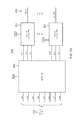
[0017]レベルシフタとしても機能するワードラインデコーダはメモリ動作スピードを増すために提供される。複数のワードライン(WL)を含む例示メモリ200が図2Aに示される。メモリ200において、第1のワードライン(WL−1)から最終ワードライン(WL−256)に及ぶ256ワードラインがある。しかしながら、代替態様では、ワードラインの数は256を超えるまたは未満であり得る。したがって、8ビットアドレス203は256ワードラインのいずれか1つを選択するのに十分である。アドレス203は第1のアドレスビットA1乃至最後のアドレスビットA8に及ぶ。ロジックパワードメイン(logic-power-domain)行デコーダ202はアドレス203をデコードする。ロジックパワードメインはロジックパワーサプライ電圧VDDLにより電力供給される。したがって、行デコーダ202はロジックパワーサプライ電圧VDDLを供給するロジックドメインパワーサプライノードに結合される。行デコーダ202と対照的に、複数のデコーダレベルシフタ201は、ロジックパワーサプライ電圧VDDLとは異なるメモリパワーサプライ電圧VDDHにより電力供給されるメモリパワードメイン内にある。一般に、ロジックパワーサプライ電圧VDDLとメモリパワーパワーサプライ電圧VDDHに関する相対レベルはメモリ200を含む集積回路に関する動作モードに依存するであろう。
[0017] A word line decoder that also functions as a level shifter is provided to increase memory operating speed. An
[0018]ロジックパワードメインがハイパワーモードにあるのに対して、メモリパワードメインがロウパワー動作モードにある場合、ロジックパワーサプライ電圧VDDLはメモリパワーサプライ電圧より高いかもしれない。反対にロジックパワードメインがスタンバイまたはロウパワー動作モードにある場合、メモリパワーサプライ電圧VDDHはロジックパワーサプライ電圧VDDLよりも高いかもしれない。一般に、ロジックパワーサプライ電圧VDDLは典型的にメモリパワーサプライ電圧よりも低いので以下の説明はメモリパワーサプライ電圧VDDHは実際にはロジックパワーサプライ電圧VDDLよりも大きいと仮定する。しかしながら、ここに開示されたレベルシフトはまたワードラインを駆動することに関して振幅におけるレベルシフトダウンに適用可能であることが理解されよう。 [0018] When the logic power domain is in the high power mode while the memory power domain is in the low power mode of operation, the logic power supply voltage VDDL may be higher than the memory power supply voltage. Conversely, when the logic power domain is in standby or low power operation mode, the memory power supply voltage VDDH may be higher than the logic power supply voltage VDDL. In general, since the logic power supply voltage VDDL is typically lower than the memory power supply voltage, the following description assumes that the memory power supply voltage VDDH is actually greater than the logic power supply voltage VDDL. However, it will be appreciated that the level shift disclosed herein is also applicable to level shift down in amplitude with respect to driving word lines.
[0019]アドレス203のような相対的に広いアドレスをデコードする場合、全体のアドレスを各ワードラインに個別に対応する単一のデコードされた信号にデコードすることは極めて非効率である。言い換えれば、デコードされた信号が1対1でワードラインと対応するように行デコーダ202はアドレスビット203を256の異なるデコードされた信号にデコードすることは考えられ得る。しかし、そのような広範囲のデコーディングは遅くかつ非効率であろう。従って、行デコーダ202はアドレスビットのサブセットを複数の対応するデコードされた信号にデコードするように構成される。メモリ200において、デコーダ202は3つのアドレスビット(例えば、アドレスビット(A1、A2、およびA3)をra−1乃至ra−8に及ぶraデコード信号にデコードするように構成される。同様に、デコーダ202は別の3つのアドレスビット(例えば、アドレスビットA4、A5およびA6)をrb−1乃至rb−8(図示せず)に及ぶrbデコード信号にデコードするように構成される。最後に、デコーダ202はアドレスビットA7およびA8のような残りの2つのアドレスビットをs rc−1乃至rc−4に及ぶrcデコード信号にデコードするように構成される。
[0019] When decoding a relatively wide address, such as
[0020]したがって、デコーダ202は並列に動作している(running)3つの異なるデコーダを含むとみなされることができる。デコーダ202内の第1の3ビットデコーダ(図示せず)は対応するデコード信号ra−1乃至ra−8(ra信号)を生成する。デコーダ202内の第2の3ビットデコーダは対応するデコード信号rb−1乃至rb−8(rb信号)を生成する。最後に、デコーダ202内の2ビットデコーダは対応するデコード信号rc−1乃至rc−4(rc信号)を生成する。デコード信号に関して各ワードラインは独自の対応するデコーダレベルシフタ201を有する。したがって、256ワードラインに対応する256デコーダレベルシフタ201がある。ビットセルバンクに構成されるインプリメンテーションにおいて、1つのデコーダレベルシフタ201は右ワードラインおよび左ワードラインのような1対のワードラインに対応することができる。しかし、各バンク内では、デコーダレベルシフタに対するワードラインの対応はメモリ200に関して示されるように1対1である。
[0021]256のデコーダレベルシフタ201があるので、各デコードされたra信号に関して256/8=32のデコーダレベルシフタがある。したがって、32のデコーダレベルシフタ201の1つのグループはデコードされたra−1信号を受信するであろう。32のデコーダレベルシフタ201の別のグループは32のデコーダレベルシフタ201の最終グループがデコードされたra−8信号を受信するようにデコードされたra−2信号を受信する、等々であろう。デコーダレベルシフタ201の類似のグルーピングはデコードされたrb信号に関してなされることができる。デコードされたrc信号に関して、rc信号は2つのアドレスビットをデコードすることから生じるという事実により、デコーダレベルシフタ201の4つのグループがあるのみであろう。この結果、各デコーダレベルシフタ201はデコードされた信号ra、rbおよびrcの固有の一意的な(its own unique)セットを受信する。
[0020] Accordingly, the
[0021] Since there are 256
[0022]結果として生じるデコードされたra、rbおよびrcの分配において、デコーダレベルシフタ201とその対応するワードラインとの間の1対1の対応があるのと同じように、デコードされた信号とデコーダレベルシフタ201のいかなる所与のインスタンシエーション(instantiation)の間にも1対1の対応がある。例えば、デコードされたra−1、rb−1およびrc−1のセットを受信する唯一つのデコーダレベルシフタ201がある。デコードされた信号の少なくとも1つは残りのデコーダレベルシフタ201のすべてに関して異なるであろう。例えば、他の(another)デコーダレベルシフタ(図示せず)はデコードされた信号ra−1およびrc−1を受信することができるがデコードされた信号rb−1は受信することができないであろう。そのかわり、この他の(this other)デコーダレベルシフタは残りのデコードされた信号rb−2乃至rb−8の1つを受信しなければならない。この態様において、各デコーダレベルシフタ201はアドレス信号203が一意的に各ワードラインを識別することができるようにデコードされた信号の固有の組み合わせまたはセットを受信する。
[0022] In the resulting decoded ra, rb and rc distribution, the decoded signal and the decoder are the same as there is a one-to-one correspondence between the
[0023]メモリ200と対照的に、一般的なメモリは各デコーダレベルシフタ201をANDゲートのようなロジックパワードメイン(logic-power-domain)デコーダで置き換えるであろう。その点に関して、行デコーダ202は選択されたワードラインに関して各デコードされた信号をアサートするように機能する。例えば、行デコーダ202は、ワードラインWL−1を選択するためにロジックパワーサプライ電圧VDDLにデコードされた信号ra−1、rb−1およびrc−1の各々をアサートするであろう。従って、一般的なVDDLパワーANDゲートはアサートされたデコード信号のセットを受信することに応答してその出力をハイにドライブするであろう。このANDゲート出力は次に図1に関して説明したレベルシフタ100によるようなメモリパワードメインに関するVDDHにレベルシフトされる必要があるであろう。しかし、この一般的なレベルシフトは上述したように低速でありかつ過度の電力を消費する。対照的に、デコーダレベルシフタ201は高速でありかつ電力消費が少ない。
[0023] In contrast to
[0024]これらの利点のある特徴を提供するために、各デコーダレベルシフタ201は図2Bに示されるようにインプリメントされることができる。NANDゲート205のような第1のロジックゲートは特定のデコーダレベルシフタ201に割り当てられたra、rbおよびrc信号のデコードされたセットを処理する。デコードされた信号ra、rbおよびrcの集合はこれらのデコードされた信号の256の異なるインスタンシエーションの1つを表す。ra、rb、またはrcのような任意の個別のデコードされた信号に関して、デコーディングは終了される。たとえば、メモリ200(図2A)内の行デコーダ202はデコードされた信号ra−1乃至ra−8の1つをアサートするために3つのアドレスビットをデコードする。適切にデコードされた信号raのアサーションに関して為されるべきさらなるデコーディングはない。しかし、各デコーダレベルシフタ201はそのセット内の各デコードされた信号ra、rbおよびrcがアサートされるかどうかを決定するように機能する。したがって、この処理ステージはデコードされた信号ra、rbおよびrcのグループに関してである。行デコーダ202は従って個々のデコーディングを実行するのに対して各デコーダレベルシフタ201はグループデコーディングまたは処理を実行するように考慮されることができる。
[0024] In order to provide these advantageous features, each
[0025]このグループデコーディングに関して、そのセット内の各デコードされた信号ra、rbおよびrcがアサートされる場合(行デコーダ202によってロジックパワーサプライ電圧VDDLにチャージされる)、NANDゲート205はNAND出力ノード206(ワードラインドライバノード)上を転送される(carried on)NAND出力信号をディスチャージするであろう。メモリパワードメインインバータ210は、デコードされた信号ra、rbおよびrcのセットがすべてアサートされるとワードライン225をメモリパワーサプライ電圧VDDHに対してハイにチャージするためにNAND出力信号を反転する。NANDゲート205は、PMOSトランジスタP1のようなスイッチを介してメモリパワーサプライ電圧VDDHを供給するメモリドメインパワーサプライノードに結合する。トランジスタP1のソースはメモリドメインパワーサプライノードに結合し一方そのドレインはNANDゲート205のパワーサプライ入力ノードに結合する。NORゲート215のような第2のロジックゲートはNAND出力信号およびリセット信号を処理することに応答してトランジスタP1が導通か非導通かを制御する。rbの補数(complement)
[0025] For this group decoding, if each decoded signal ra, rb and rc in the set is asserted (charged to the logic power supply voltage VDDL by the row decoder 202), the
![]()
![]()
のようなデコードされた信号の1つの補数としてリセット信号を形成することは便利である。その点に関して、行デコーダ202はワードラインアサーション期間の後でデコードされた信号をリセットすることに留意する必要がある。特に、行デコーダ202はアドレス203をデコードし、読み取りまたは書き込み期間の間にワードアサーション期間に適切なデコードされた信号をアサートする。ワードラインアサーション期間が終了された後、次に行デコーダ202はワードラインがデアサート(de-asserted)されるようにすべてのデコードされた信号をデフォルトゼロ(ディスチャージされた値)にリセットする。したがって、ワードラインのセット内のすべてのデコードされた信号ra, rbおよびrcはワードラインアサーションの後ゼロにリセットされるのでどのデコードされた信号がリセット信号とし選択されるかは問題ではない。
It is convenient to form the reset signal as one's complement of a decoded signal such as In that regard, it should be noted that the
[0026]NORゲート215はトランジスタP1のゲートを駆動するNOR出力ノード211でフィードバック信号を生成するためにNAND出力信号とリセット信号を処理する。セット内のデコードされた信号ra、rb、rcの各々がアサートされると、リセット信号はNAND出力信号とともにロウになるであろう。NORゲート215はメモリパワードメイン内にあるので、NORゲート215は次にメモリパワーサプライ電圧VDDHへのフィードバック信号をアサートするであろう。メモリパワーサプライ電圧VDDHからNANDゲート205を絶縁するためにフィードバック信号のアサーションによってトランジスタP1は完全にオフになる。
[0026] The NOR
[0027]NANDゲート205は図3に示されるようにインプリメントされることができる。NAND出力ノード206はPMOSトランジスタP3とPMOSトランジスタP4に並列に配列されたPMOSトランジスタP2を介してトランジスタP1のドレインに結合する。トランジスタP2、P3、およびP4のソースはNANDゲート205に関するパワーサプライ入力ノードを形成する。デコードされた信号raはトランジスタP2のゲートを駆動する。同様に、デコードされた信号rbはトランジスタP3のゲートを駆動し、一方デコードされた信号rcはトランジスタP4のゲートを駆動する。NAND出力ノード206はNMOSトランジスタM1、NMOSトランジスタM2およびNMOSトランジスタM3の直列アレイを介してグラウンドに結合する。デコードされた信号raはトランジスタM1のゲートを駆動する。同様に、デコードされた信号rbはトランジスタM2のゲートを駆動し、一方デコードされた信号rcはトランジスタM3のゲートを駆動する。デコードされた信号ra、rb、rcはVDDLパワーサプライ電圧にのみアサートされるロジックドメイン信号である。それらのソースがパワーサプライノードに直接結合するなら、デコードされた信号ra、rb、rcがすべてそれらのロジックパワーサプライ電圧VDDLにアサートされるとメモリパワードメイントランジスタP1、P2、P3はすべて弱くオンになる(be weakly on)であろう。トランジスタP2、P3、P4は次にNAND出力ノード206のディスチャージの期間にトランジスタM1、M2およびM3と競合する(fight with)可能性があるであろう。したがって、トランジスタP1のスイッチングオフによってNAND出力ノード206のディスチャージの期間にメモリパワーサプライ電圧VDDHからトランジスタP2,P3、およびP4を絶縁することは電力を節約し、メモリ動作スピードを高める点で極めて有利である。
[0027] The
[0028]一般に、NANDゲート205内のP2、P3、およびP4のような並列に配列されたPMOSトランジスタの数はデコードされた信号の数に依存し、それは次にアドレス信号203に間接的に依存する(図1)。同様に、M1、M2およびM3のような直列に配列されたNMOSトランジスタの数もデコードされた信号の数、したがってアドレス信号203の幅に依存子し、それは次にメモリ200内のワードの数に依存する。Nのデコードされた信号(Nは複数の整数)を有する実施形態において、NANDゲート205は次にNAND出力ノード206とトランジスタP1のドレインとの間に並列に配列されたN個のPMOSトランジスタを含むことができる。N個のPMOSトランジスタはデコーダレベルシフタ201に関するデコードされた信号のセット内のデコードされた信号に1対1で対応する。各デコードされた信号はその対応するPMOSトランジスタのゲートを駆動する。同様に、同じ実施形態はNAND出力ノード206とグラウンドとの間に並列に配列されたN個のNMOSトランジスタを含むであろう。N個のNMOSトランジスタはセット内の各デコードされた信号は対応するNMOSトランジスタのゲートを駆動するようにデコードされた信号に1対1で対応するであろう。
[0029]NANDゲート205がNAND出力ノード206に関してNANDゲート205がどのように配列されるかに比べて相補的な態様でNOR出力ノード211に関してNORゲート215が配列される。特に、メモリパワーサプライ電圧VDDHを供給するメモリパワーサプライノードとNOR出力ノード211との間に直列に配列されたPMOSトランジスタP5とPMOSトランジスタP6が直接に配列される。反対に、NMOSトランジスタM4とNMOSトランジスタM5はグラウンドとNOR出力ノード211との間に並列に配列される。NAND出力信号はトランジスタP6とM4とを駆動する。同様に、リセット信号はトランジスタP5とM5のゲートを駆動する。デコードされた信号ra、rb、rcがアサートされると、リセット信号は、トランジスタM5を遮断し、トランジスタP5をスイッチオンするためにディスチャージされる。トランジスタM1、M2およびM3がすべて導通するので、NAND出力信号はディスチャージされ、それはトランジスタP6をスイッチオンし、トランジスタM4を遮断する。トランジスタP5とP6が導通するので、NOR出力ノード211上を転送されるフィードバック信号はメモリパワーサプライ電圧VDDHにチャージされる。ロジックパワーサプライ電圧VDDLがメモリパワーサプライ電圧VDDHよりも十分に低い場合、トランジスタP2、P3およびP4はデコードされた信号がすべてアサートされると弱くオンになるであろう(weakly on)。しかし、VDDHパワーサプライ電圧へのフィードバック信号のチャージは、トランジスタP2、P3およびP4がNAND出力信号のディスチャージに関してトランジスタM1、M2およびM3と競合(struggle with)できないようにトランジスタP1をスイッチオフする。PMOSトランジスタP1とNORゲート215の組み合わせは、デコードされた信号の1つのリセットに応答してメモリパワーサプライ電圧VDDHからNANDゲート205を絶縁し、デコードされた信号の1つのアサーションに応答してNANDゲートを第2のパワーサプライ電圧に結合する手段を備えるとみなすことができる。
[0028] Generally, the number of PMOS transistors arranged in parallel, such as P2, P3, and P4 in
[0029] NOR
[0030]インバータ210はNMOSトランジスタM6と直列にPMOSトランジスタP7を備える。トランジスタP7とM6に関するドレインはワードラインに結合する。NAND出力信号はトランジスタP7とM6の両方のゲートを駆動する。トランジスタP7のソースはメモリドメインパワーサプライノードに結合されているので、NAND出力信号がディスチャージされると、トランジスタP7は次にワードラインをメモリパワーサプライ電圧VDDHにチャージする。読取または書き込み動作が終了すると、デコードされた信号は次にリセットされる(グラウンドにディスチャージされる)。リセット信号は次にトランジスタM5をスイッチオンするようにアサートされ、それはトランジスタP1をスイッチオンするためにフィードバック信号をディスチャージする。トランジスタP2、P3およびP4は次にNAND出力信号をメモリパワーサプライ電圧VDDHにチャージすることができる。したがって、ワードラインをディスチャージするようにNAND出力信号のアサーションに応答してトランジスタM6がスイッチオンされる。
[0030] The
[0031]結果として生じるデコーダレベルシフタ201はレベルシフタ100のような一般的なレベルシフタが続く各ワードラインに関する一般的なグループデコーダの使用に比べて非常に有利である。特に、デコーダレベルシフタ201にNMOS/PMOS競合(struggle)が存在しないので、メモリ動作スピードは一般的なレベルシフタ100の使用に関して有利に増加される。さらに、NMOS/PMOS競合の消去はクローバ(crowbar)電流の関連づけられたディスチャージを消去するので、この増加された動作スピードはパワーセービングの増加を伴う(come with)。デコーダレベルシフタを含むメモリに関する動作の方法が以下に説明される。
[0031] The resulting
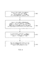
[0032]図4は本開示の観点に従うデコーダレベルシフタに関する動作の例示方法に関するフローチャートである。行為(act)400は第1のパワーサプライ電圧により電力供給される第1のパワードメインで実行され、複数のデコードされた信号を第1のパワーサプライ電圧にアサートするために第1のアドレス信号をデコードすることを備える。デコードされた信号ra、rbおよびrcを生成するために行デコーダ202によるアドレス203のデコーディングは行為400の一例である。方法は、また第1のパワーサプライ電圧よりも大きい第2のパワーサプライ電圧により電力供給される第2のパワードメインにおいて実行される行為405を含み、第2のパワーサプライ電圧を供給するパワーサプライノードからワードラインドライバノードを絶縁するスイッチを動作させながらデコードされた信号のアサーションに応答してワードラインドライバノードをディスチャージすることを備える。トランジスタP1がスイッチオフされる間にNAND出力ノード206をディスチャージすることは行為405の一例である。方法はまたワードラインドライバノードのディスチャージに応当する行為410を含み第2のパワードメイン内のワードラインに関する電圧を第2のパワーサプライ電圧にチャージすることを備える。ワードライン225のアサーションは行為410の一例である。最後に、方法はデコードされた信号の少なくとも1つのディスチャージに応当して行為415を含みスイッチを閉じてワードラインドライバノードをパワーサプライノードにチャージすることを備える。トランジスタP1が導通している間にNAND出力ノード206をチャージすることは行為415の一例である。
[0032] FIG. 4 is a flowchart of an example method of operation for a decoder level shifter in accordance with aspects of the present disclosure. An
[0033]当業者が、近い将来に特定のアプリケーションを現時点で理解することとなり、依存していることとなる時、多くの修正、代替および変形は、それの主旨および範囲から逸脱することなく、本開示のデバイスの使用の方法、構成、装置、およびマテリアルにおよびそれらの中になされることができる。このことを踏まえて、本開示の範囲は、単にそれらのいくつかの例として、本明細書で例示され、説明された特定の実施形態のそれに、限定されるべきでなく、むしろ、以下に添付された特許請求の範囲のそれに十分に相応するべきである。
以下に本願の出願当初の特許請求の範囲に記載された発明を付記する。
[C1]
第1の複数のデコードされた信号を第1のパワーサプライ電圧にアサーションすることに応答してワードラインドライバノードをディスチャージするように構成された第1のロジックゲートと、
ワードラインと、
第2のパワーサプライ電圧により電力供給されるインバータと、ここにおいて前記インバータはワードラインドライバノードの電圧をワードラインに関するワードライン電圧に反転するように構成される、
第1のロジックゲートへのパワーサプライ入力ノードと前記第2のパワーサプライ電圧に関するパワーサプライノードとの間に結合されたスイッチと、
前記ワードラインドライバノードと前記第1の複数のデコードされた信号内の前記デコードされた信号の1つの補数に応答して前記スイッチをスイッチオフするように構成された第2のロジックゲートと、
を備えた回路。
[C2]
前記第1のロジックゲートはNANDゲートを備える、C1の回路。
[C3]
前記NANDゲートは前記第1の複数のデコードされた信号に対応する第1の複数のPMOSトランジスタを備え、ここにおいて、前記第1の複数のPMOSトランジスタ内の各PMOSトランジスタは前記パワーサプライ入力ノードに結合されたソースと、前記ワードラインドライバノードに結合されたドレインと、前記対応するデコードされた信号により駆動されるゲートを含む、C1の回路。
[C4]
前記NANDゲートは、前記第1の複数のデコードされた信号に対応する第1の複数のNMOSトランジスタをさらに備え、前記第1の複数のNMOSトランジスタは前記ワードラインドライバノードとグラウンドとの間に直列に配列され、前記第1の複数のNMOSトランジスタ内の各NMOSトランジスタは前記対応するデコードされた信号により駆動されるゲートを有する、C3の回路。
[C5]
前記第2のロジックゲートは前記第2のパワーサプライ電圧により電力供給されるNORゲートを備える、C1の回路。
[C6]
前記スイッチは、ソースが前記パワーサプライノードに結合されドレインが前記パワーサプライ入力ノードに結合され第1のPMOSトランジスタを備え、前記NORゲートの出力は前記第1のPMOSトランジスタのゲートに結合する、C5の回路。
[C7]
前記NORゲートは第3のPMOSトランジスタに直列な第2のPMOSトランジスタを備え、
前記第2のPMOSトランジスタは前記パワーサプライノードに結合されたソースと、前記第3のPMOSトランジスタのソースに結合されたドレインと前記デコードされた信号の1つの補数(complement)により駆動されるように構成されるゲートを有し、
前記第3のPMOSトランジスタは前記NORゲートの前記出力に結合されたドレインと前記ワードラインドライバノードに結合されたゲートを有する、C6の回路。
[C8]
前記NORゲートは、グラウンドに結合されたソースと、前記ワードラインドライバノードに結合されたゲートと、前記NORゲートの前記出力に結合されたドレインを有する第1のNMOSトランジスタをさらに備え、
前記NORゲートは、グラウンドに結合されたソースと、前記NORゲートの前記出力に結合されたドレインと、前記デコードされた信号の1つの補数により駆動されるように構成されたゲートを有する第2のNMOSトランジスタをさらに備える、C7の回路。
[C9]
前記第1の複数のデコードされた信号を提供するために複数のアドレス信号をデコードするように構成された行デコーダをさらに備えた、C1の回路。
[C10]
前記行デコーダは前記複数のアドレス信号を複数のセットのデコードされた信号にデコードするようにさらに構成され、
前記第1の複数のデコードされた信号は前記デコードされた信号の複数のセット内のデコードされた信号の各セットから1つのデコードされた信号を備える、C9の回路。
[C11]
第1のパワーサプライ電圧により電力供給される第1のパワードメインにおいて、複数のデコードされた信号を前記第1のパワーサプライ電圧にアサートするためにアドレス信号をデコードすることと、
第2のパワーサプライ電圧により電力供給される第2のパワードメインにおいて、前記第2のパワーサプライ電圧を供給するパワーサプライノードから前記ワードラインドライバノードを絶縁するためにスイッチを開放している間前記複数のデコードされた信号のアサーションに応答してワードラインドライバノードをディスチャージすることと、
前記ワードラインドライバノードの前記ディスチャージに応当して、前記第2のパワードメイン内のワードラインに関する電圧を前記第2のパワーサプライ電圧にチャージすることと、
前記複数のデコードされた信号内の前記デコードされた信号の少なくとも1つのディスチャージに応当して、前記スイッチを閉成し、前記ワードラインドライバノードを前記第2のパワーサプライ電圧にチャージすることと、
を備えた方法。
[C12]
前記第2のパワーサプライ電圧は前記第1のパワーサプライ電圧よりも大きい、C11の方法。
[C13]
ワードラインドライバノードを第2のパワーサプライ電圧にチャージすることに応答して前記ワードラインをディスチャージすることをさらに備えた、C11の方法。
[C14]
NORゲート出力信号を生成するために前記第2のパワーサプライ電圧により電力供給されるNORゲートにおいて前記ワードラインドライバノードの電圧と前記デコードされた信号の前記1つの補数をNORすることをさらに備え、
前記スイッチを閉成することは前記NORゲート出力信号のディスチャージに応当する、C11の方法。
[C15]
前記スイッチの開放は前記第2のパワーサプライ電圧への前記NORゲート出力のチャージングに応答する、C14の方法。
[C16]
前記ワードラインドライバノードを制御するNANDゲート出力信号を生成するために前記スイッチを介して電力供給されるNANDゲート内の複数のデコードされた信号のNANDをとることをさらに備え、
前記ワードラインドライバノードを前記第2のパワーサプライ電圧にチャージすることは、前記NANDゲート出力信号を前記第2のパワーサプライ電圧へ駆動することを備える、C14の方法。
[C17]
前記ワードラインドライバノードをディスチャージすることは前記NANDゲート出力信号をディスチャージすることを備える、C16の方法。
[C18]
複数のデコードされた信号を生成するために複数のアドレス信号をデコードするように構成された行デコーダと、ここにおいて、前記行デコーダは、第1のパワーサプライ電圧により電力供給される第1のパワードメイン内にある、
NANDゲート出力信号を生成するために前記複数のデコードされた信号のNANDをとるように構成されたNANDゲートと、ここにおいて前記NANDゲートは第2のパワーサプライ電圧により電力供給される第2のパワードメイン内にある、
前記複数のデコードされた信号内の前記デコードされた信号の1つのリセットに応答して前記第2のパワーサプライ電圧から前記NANDゲートを絶縁し、前記デコードされた信号の1つのアサーションに応答して前記第2のパワーサプライ電圧に前記NANDゲートを結合する手段と、
ワードラインと、および
前記NANDゲート出力信号のディスチャージに応当して前記第2のパワーサプライ電圧に前記ワードラインの電圧をアサートするように構成されたワードラインドライバと、を備えた、メモリ。
[C19]
前記ワードラインドライバは、前記第2のパワーサプライ電圧により電力供給されるインバータを備える、C18のメモリ。
[C20]
前記手段は、NORゲートとスイッチトランジスタを備える、C18のメモリ。
[0033] Many modifications, substitutions and variations will occur to those skilled in the art without departing from the spirit and scope thereof, when a particular application will be understood and relied upon in the near future. Methods, configurations, apparatus, and materials of use of the devices of the present disclosure can be made and within them. In light of this, the scope of the present disclosure should not be limited to that of the specific embodiments illustrated and described herein, but merely as a few examples thereof, rather being attached below. And should fully correspond to that of the appended claims.
The invention described in the scope of claims at the beginning of the application of the present application will be added below.
[C1]
A first logic gate configured to discharge a word line driver node in response to asserting a first plurality of decoded signals to a first power supply voltage;
The word line,
An inverter powered by a second power supply voltage, wherein the inverter is configured to invert the voltage at the word line driver node to the word line voltage for the word line;
A switch coupled between a power supply input node to a first logic gate and a power supply node for the second power supply voltage;
A second logic gate configured to switch off the switch in response to one's complement of the decoded signal in the wordline driver node and the first plurality of decoded signals;
Circuit with.
[C2]
The circuit of C1, wherein the first logic gate comprises a NAND gate.
[C3]
The NAND gate includes a first plurality of PMOS transistors corresponding to the first plurality of decoded signals, wherein each PMOS transistor in the first plurality of PMOS transistors is connected to the power supply input node. The circuit of C1, including a coupled source, a drain coupled to the word line driver node, and a gate driven by the corresponding decoded signal.
[C4]
The NAND gate further includes a first plurality of NMOS transistors corresponding to the first plurality of decoded signals, wherein the first plurality of NMOS transistors are connected in series between the word line driver node and ground. A circuit of C3, wherein each NMOS transistor in the first plurality of NMOS transistors has a gate driven by the corresponding decoded signal.
[C5]
The circuit of C1, wherein the second logic gate comprises a NOR gate powered by the second power supply voltage.
[C6]
The switch comprises a first PMOS transistor having a source coupled to the power supply node and a drain coupled to the power supply input node, the output of the NOR gate being coupled to the gate of the first PMOS transistor, C5 Circuit.
[C7]
The NOR gate comprises a second PMOS transistor in series with a third PMOS transistor,
The second PMOS transistor is driven by a source coupled to the power supply node, a drain coupled to the source of the third PMOS transistor, and one complement of the decoded signal. Having a gate configured;
The C6 circuit, wherein the third PMOS transistor has a drain coupled to the output of the NOR gate and a gate coupled to the word line driver node.
[C8]
The NOR gate further comprises a first NMOS transistor having a source coupled to ground, a gate coupled to the word line driver node, and a drain coupled to the output of the NOR gate;
The NOR gate has a source coupled to ground, a drain coupled to the output of the NOR gate, and a gate configured to be driven by one's complement of the decoded signal. The C7 circuit, further comprising an NMOS transistor.
[C9]
The circuit of C1, further comprising a row decoder configured to decode a plurality of address signals to provide the first plurality of decoded signals.
[C10]
The row decoder is further configured to decode the plurality of address signals into a plurality of sets of decoded signals;
The circuit of C9, wherein the first plurality of decoded signals comprises one decoded signal from each set of decoded signals in the plurality of sets of decoded signals.
[C11]
Decoding an address signal to assert a plurality of decoded signals to the first power supply voltage in a first power domain powered by a first power supply voltage;
In a second power domain powered by a second power supply voltage, while the switch is opened to isolate the word line driver node from the power supply node supplying the second power supply voltage Discharging the word line driver node in response to assertions of the plurality of decoded signals;
Responsive to the discharge of the word line driver node, charging a voltage associated with a word line in the second power domain to the second power supply voltage;
Responsive to at least one discharge of the decoded signal in the plurality of decoded signals, closing the switch and charging the word line driver node to the second power supply voltage;
With a method.
[C12]
The method of C11, wherein the second power supply voltage is greater than the first power supply voltage.
[C13]
The method of C11, further comprising discharging the word line in response to charging the word line driver node to a second power supply voltage.
[C14]
Further NORing the voltage of the word line driver node and the one's complement of the decoded signal at a NOR gate powered by the second power supply voltage to generate a NOR gate output signal;
The method of C11, wherein closing the switch corresponds to discharging of the NOR gate output signal.
[C15]
The method of C14, wherein opening the switch is responsive to charging of the NOR gate output to the second power supply voltage.
[C16]
Further comprising taking a NAND of a plurality of decoded signals in a NAND gate powered through the switch to generate a NAND gate output signal that controls the word line driver node;
The method of C14, wherein charging the wordline driver node to the second power supply voltage comprises driving the NAND gate output signal to the second power supply voltage.
[C17]
The method of C16, wherein discharging the word line driver node comprises discharging the NAND gate output signal.
[C18]
A row decoder configured to decode a plurality of address signals to generate a plurality of decoded signals, wherein the row decoder is powered by a first power supply voltage; In the domain,
A NAND gate configured to take a NAND of the plurality of decoded signals to generate a NAND gate output signal, wherein the NAND gate is powered by a second power supply voltage; In the domain,
In response to resetting one of the decoded signals in the plurality of decoded signals, isolating the NAND gate from the second power supply voltage, and in response to one assertion of the decoded signal Means for coupling the NAND gate to the second power supply voltage;
Word line, and
A memory comprising: a word line driver configured to assert the word line voltage to the second power supply voltage in response to discharge of the NAND gate output signal.
[C19]
The memory of C18, wherein the word line driver includes an inverter powered by the second power supply voltage.
[C20]
The means comprises a C18 memory comprising a NOR gate and a switch transistor.
Claims (19)
ワードラインと、
第2のパワーサプライ電圧により電力供給されるインバータと、ここにおいて、前記インバータは、前記ワードラインドライバノードの電圧を前記ワードラインに関するワードライン電圧に反転するように構成される、
前記第1のロジックゲートへのパワーサプライ入力ノードと前記第2のパワーサプライ電圧に関するパワーサプライノードとの間に結合されたスイッチと、
前記ワードラインドライバノードの前記ディスチャージと前記第1の複数のデコードされた信号内の前記デコードされた信号のうちの1つの補数のディスチャージとに応答して前記スイッチをスイッチオフするように構成された第2のロジックゲートと、ここにおいて、前記第2のパワーサプライ電圧は、前記第1のパワーサプライ電圧よりも大きい、
を備えた回路。 A first logic gate configured to discharge the word line driver node in response to the assertion of the first power supply voltage of the first plurality of decoded signals,
The word line,
An inverter which is powered by the second power supply voltage, wherein the inverter is configured a voltage of the word line driver node to invert the word line voltage for said word lines,
A switch coupled between the power supply node for power supply input node and said second power supply voltage to the first logic gate,
Said switch configured to switch off in response to the discharge of the one's complement of said decoded signal in said discharge and said first plurality of decoded signals of the word line driver node A second logic gate , wherein the second power supply voltage is greater than the first power supply voltage;
Circuit with.
第2のパワーサプライ電圧により電力供給される第2のパワードメインにおいて、前記第2のパワーサプライ電圧を供給するパワーサプライノードからワードラインドライバノードを絶縁するためにスイッチを開放している間、前記複数のデコードされた信号の前記アサーションに応答して前記ワードラインドライバノードをディスチャージすることと、
前記ワードラインドライバノードの前記ディスチャージに応当して、前記第2のパワードメイン内のワードラインに関する電圧を前記第2のパワーサプライ電圧にチャージすることと、
前記複数のデコードされた信号内の前記デコードされた信号の少なくとも1つのディスチャージに応当して、前記スイッチを閉成し、前記ワードラインドライバノードを前記第2のパワーサプライ電圧にチャージすることと、ここにおいて、前記第2のパワーサプライ電圧は、前記第1のパワーサプライ電圧よりも大きい、
を備えた方法。 Decoding an address signal to assert a plurality of decoded signals to the first power supply voltage in a first power domain powered by a first power supply voltage;
In the second power domain that is powered by the second power supply voltage, while opening the switch to isolate the power supply node or Lawah over de line driver node supplying said second power supply voltage , the method comprising discharging the word line driver node in response to the assertion of the plurality of decoded signals,
Responsive to the discharge of the word line driver node, charging a voltage associated with a word line in the second power domain to the second power supply voltage;
Responsive to at least one discharge of the decoded signal in the plurality of decoded signals, closing the switch and charging the word line driver node to the second power supply voltage; Here, the second power supply voltage is larger than the first power supply voltage.
With a method.
NANDゲート出力信号を生成するために前記複数のデコードされた信号のNANDをとるように構成されたNANDゲートと、ここにおいて、前記NANDゲートは、第2のパワーサプライ電圧により電力供給される第2のパワードメイン内にあり、前記第2のパワーサプライ電圧は、前記第1のパワーサプライ電圧よりも大きい、
前記複数のデコードされた信号内の前記デコードされた信号のうちの1つのリセットに応答して前記第2のパワーサプライ電圧から前記NANDゲートを絶縁し、前記デコードされた信号のうちの前記1つのアサーションに応答して前記第2のパワーサプライ電圧に前記NANDゲートを結合する手段と、
ワードラインと、
前記NANDゲート出力信号のディスチャージに応当して前記第2のパワーサプライ電圧に前記ワードラインの電圧をアサートするように構成されたワードラインドライバと、
を備えた、メモリ。 A row decoder configured to decode a plurality of address signals to generate a plurality of decoded signals, wherein the row decoder is powered by a first power supply voltage; In the domain,
A NAND gate configured to take NAND of the plurality of decoded signals to generate the NAND gate output signal, wherein said NAND gate includes a first powered by the second power supply voltage 2 power domain in the near of is, the second power supply voltage is greater than said first power supply voltage,
To insulate the NAND gate from said second power supply voltage in response to a single reset of said decoded signal in said plurality of decoded signals, said one of said decoded signal Means for coupling the NAND gate to the second power supply voltage in response to an assertion;
The word line ,
A word line driver and anniversary configured to assert a voltage of the word line to the second power supply voltage to the discharge of the prior SL NAND gate output signal,
With a memory.
Applications Claiming Priority (5)
| Application Number | Priority Date | Filing Date | Title |
|---|---|---|---|
| US201562133840P | 2015-03-16 | 2015-03-16 | |
| US62/133,840 | 2015-03-16 | ||
| US15/070,963 US9940987B2 (en) | 2015-03-16 | 2016-03-15 | High-speed word line decoder and level-shifter |
| US15/070,963 | 2016-03-15 | ||
| PCT/US2016/022593 WO2016149333A1 (en) | 2015-03-16 | 2016-03-16 | High-speed word line decoder and level-shifter |
Publications (3)
| Publication Number | Publication Date |
|---|---|
| JP2018513520A JP2018513520A (en) | 2018-05-24 |
| JP6352552B2 true JP6352552B2 (en) | 2018-07-04 |
| JP2018513520A5 JP2018513520A5 (en) | 2018-07-05 |
Family
ID=55661580
Family Applications (1)
| Application Number | Title | Priority Date | Filing Date |
|---|---|---|---|
| JP2017548466A Expired - Fee Related JP6352552B2 (en) | 2015-03-16 | 2016-03-16 | High-speed word line decoder and level shifter |
Country Status (6)
| Country | Link |
|---|---|
| US (1) | US9940987B2 (en) |
| EP (1) | EP3271919B1 (en) |
| JP (1) | JP6352552B2 (en) |
| KR (1) | KR101956615B1 (en) |
| CN (1) | CN107430876B (en) |
| WO (1) | WO2016149333A1 (en) |
Families Citing this family (5)
| Publication number | Priority date | Publication date | Assignee | Title |
|---|---|---|---|---|
| CN104811634B (en) * | 2013-12-29 | 2018-07-31 | 芯视达系统公司 | Support the compact row decoder of multiple voltage |
| US10037290B1 (en) * | 2016-06-02 | 2018-07-31 | Marvell International Ltd. | Dual-port memories and input/output circuits for preventing failures corresponding to concurrent accesses of dual-port memory cells |
| US10109365B2 (en) * | 2016-11-28 | 2018-10-23 | Taiwan Semiconductor Manufacturing Company Limited | Word line driver |
| US11114148B1 (en) * | 2020-04-16 | 2021-09-07 | Wuxi Petabyte Technologies Co., Ltd. | Efficient ferroelectric random-access memory wordline driver, decoder, and related circuits |
| US11264093B1 (en) * | 2020-08-25 | 2022-03-01 | Taiwan Semiconductor Manufacturing Company Limited | Duo-level word line driver |
Family Cites Families (14)
| Publication number | Priority date | Publication date | Assignee | Title |
|---|---|---|---|---|
| JP2000187977A (en) | 1998-12-21 | 2000-07-04 | Mitsubishi Electric Corp | Semiconductor memory |
| JP2004334982A (en) * | 2003-05-08 | 2004-11-25 | Nec Electronics Corp | Line decoder, semiconductor circuit device |
| JP4496069B2 (en) * | 2004-12-20 | 2010-07-07 | 株式会社東芝 | MOS type semiconductor integrated circuit device |
| US7176725B2 (en) * | 2005-02-04 | 2007-02-13 | International Business Machines Corporation | Fast pulse powered NOR decode apparatus for semiconductor devices |
| US7463545B2 (en) | 2006-03-17 | 2008-12-09 | Texas Instruments Incorporated | System and method for reducing latency in a memory array decoder circuit |
| JP2008084457A (en) | 2006-09-28 | 2008-04-10 | Toshiba Corp | Nonvolatile semiconductor memory device |
| JP2008152845A (en) * | 2006-12-15 | 2008-07-03 | Toshiba Corp | Semiconductor storage device |
| JP4913878B2 (en) * | 2009-05-27 | 2012-04-11 | ルネサスエレクトロニクス株式会社 | Word line selection circuit, row decoder |
| US8391097B2 (en) | 2010-05-25 | 2013-03-05 | Taiwan Semiconductor Manufacturing Co. Ltd. | Memory word-line driver having reduced power consumption |
| KR101753251B1 (en) | 2010-07-23 | 2017-07-05 | 삼성전자주식회사 | Static random access memory device including negative voltage level shifter |
| US8456946B2 (en) | 2010-12-22 | 2013-06-04 | Intel Corporation | NAND logic word line selection |
| US9299395B2 (en) | 2012-03-26 | 2016-03-29 | Intel Corporation | Methods and systems to selectively boost an operating voltage of, and controls to an 8T bit-cell array and/or other logic blocks |
| CN103871458B (en) | 2012-12-07 | 2018-05-01 | 三星电子株式会社 | Integrated circuit and its data processing method, decoder, memory |
| US8971133B1 (en) | 2013-09-26 | 2015-03-03 | Arm Limited | Memory device and method of operation of such a memory device |
-
2016
- 2016-03-15 US US15/070,963 patent/US9940987B2/en active Active
- 2016-03-16 KR KR1020177025630A patent/KR101956615B1/en active IP Right Grant
- 2016-03-16 EP EP16714646.3A patent/EP3271919B1/en active Active
- 2016-03-16 WO PCT/US2016/022593 patent/WO2016149333A1/en active Application Filing
- 2016-03-16 CN CN201680015459.6A patent/CN107430876B/en active Active
- 2016-03-16 JP JP2017548466A patent/JP6352552B2/en not_active Expired - Fee Related
Also Published As
| Publication number | Publication date |
|---|---|
| KR20170128299A (en) | 2017-11-22 |
| JP2018513520A (en) | 2018-05-24 |
| US20160276005A1 (en) | 2016-09-22 |
| WO2016149333A1 (en) | 2016-09-22 |
| CN107430876A (en) | 2017-12-01 |
| EP3271919B1 (en) | 2019-05-01 |
| CN107430876B (en) | 2020-12-11 |
| US9940987B2 (en) | 2018-04-10 |
| KR101956615B1 (en) | 2019-03-11 |
| EP3271919A1 (en) | 2018-01-24 |
Similar Documents
| Publication | Publication Date | Title |
|---|---|---|
| JP6352552B2 (en) | High-speed word line decoder and level shifter | |
| US9928901B2 (en) | SRAM with first and second precharge circuits | |
| US7560970B2 (en) | Level shifter | |
| US8299831B2 (en) | Semiconductor device | |
| US6842046B2 (en) | Low-to-high voltage conversion method and system | |
| CN112583383B (en) | High-speed level shift multiplexer | |
| US20170237435A1 (en) | Apparatuses and methods for voltage level control | |
| US7982505B2 (en) | Logic circuit, address decoder circuit and semiconductor memory | |
| WO2017030828A1 (en) | Dynamic voltage level shifters employing pulse generation circuits, and related systems and methods | |
| CN110495099B (en) | High-speed level shifter | |
| JP2018513520A5 (en) | ||
| US9607668B2 (en) | Systems, circuits, and methods for charge sharing | |
| WO2006059379A1 (en) | Semiconductor device employing dynamic circuit | |
| TWI455484B (en) | Level shifter | |
| KR100380778B1 (en) | Logic circuit | |
| US6559704B1 (en) | Inverting level shifter with start-up circuit | |
| US20090243693A1 (en) | Circuit for providing deterministic logic level in output circuit when a power supply is grounded | |
| KR20010085472A (en) | Logic circuit | |
| US20220013154A1 (en) | Low Power Content Addressable Memory | |
| JP2005149694A (en) | Data input/output buffer and semiconductor memory device using the buffer | |
| Viveka et al. | Energy Efficient Memory Decoder Design for Ultra-Low Voltage Systems | |
| KR20090115008A (en) | Multiplexer | |
| KR20240046980A (en) | Level shifter, and semiconductor device including the same | |
| JP2010157311A (en) | Pseudo-static dynamic bit line circuit and method | |
| US20100123500A1 (en) | Integrated circuit |
Legal Events
| Date | Code | Title | Description |
|---|---|---|---|
| A521 | Request for written amendment filed |
Free format text: JAPANESE INTERMEDIATE CODE: A523 Effective date: 20180424 |
|
| A621 | Written request for application examination |
Free format text: JAPANESE INTERMEDIATE CODE: A621 Effective date: 20180424 |
|
| A871 | Explanation of circumstances concerning accelerated examination |
Free format text: JAPANESE INTERMEDIATE CODE: A871 Effective date: 20180424 |
|
| A975 | Report on accelerated examination |
Free format text: JAPANESE INTERMEDIATE CODE: A971005 Effective date: 20180501 |
|
| TRDD | Decision of grant or rejection written | ||
| A01 | Written decision to grant a patent or to grant a registration (utility model) |
Free format text: JAPANESE INTERMEDIATE CODE: A01 Effective date: 20180508 |
|
| A61 | First payment of annual fees (during grant procedure) |
Free format text: JAPANESE INTERMEDIATE CODE: A61 Effective date: 20180606 |
|
| R150 | Certificate of patent or registration of utility model |
Ref document number: 6352552 Country of ref document: JP Free format text: JAPANESE INTERMEDIATE CODE: R150 |
|
| R250 | Receipt of annual fees |
Free format text: JAPANESE INTERMEDIATE CODE: R250 |
|
| LAPS | Cancellation because of no payment of annual fees |