JP6345407B2 - Memory system using regression analysis method and reading method thereof - Google Patents
Memory system using regression analysis method and reading method thereof Download PDFInfo
- Publication number
- JP6345407B2 JP6345407B2 JP2013220910A JP2013220910A JP6345407B2 JP 6345407 B2 JP6345407 B2 JP 6345407B2 JP 2013220910 A JP2013220910 A JP 2013220910A JP 2013220910 A JP2013220910 A JP 2013220910A JP 6345407 B2 JP6345407 B2 JP 6345407B2
- Authority
- JP
- Japan
- Prior art keywords
- read
- voltage
- data
- memory
- probability density
- Prior art date
- Legal status (The legal status is an assumption and is not a legal conclusion. Google has not performed a legal analysis and makes no representation as to the accuracy of the status listed.)
- Active
Links
Images


Classifications
-
- G—PHYSICS
- G11—INFORMATION STORAGE
- G11C—STATIC STORES
- G11C16/00—Erasable programmable read-only memories
- G11C16/02—Erasable programmable read-only memories electrically programmable
- G11C16/06—Auxiliary circuits, e.g. for writing into memory
- G11C16/26—Sensing or reading circuits; Data output circuits
-
- G—PHYSICS
- G11—INFORMATION STORAGE
- G11C—STATIC STORES
- G11C11/00—Digital stores characterised by the use of particular electric or magnetic storage elements; Storage elements therefor
- G11C11/56—Digital stores characterised by the use of particular electric or magnetic storage elements; Storage elements therefor using storage elements with more than two stable states represented by steps, e.g. of voltage, current, phase, frequency
- G11C11/5621—Digital stores characterised by the use of particular electric or magnetic storage elements; Storage elements therefor using storage elements with more than two stable states represented by steps, e.g. of voltage, current, phase, frequency using charge storage in a floating gate
- G11C11/5642—Sensing or reading circuits; Data output circuits
-
- G—PHYSICS
- G11—INFORMATION STORAGE
- G11C—STATIC STORES
- G11C16/00—Erasable programmable read-only memories
- G11C16/02—Erasable programmable read-only memories electrically programmable
- G11C16/04—Erasable programmable read-only memories electrically programmable using variable threshold transistors, e.g. FAMOS
- G11C16/0483—Erasable programmable read-only memories electrically programmable using variable threshold transistors, e.g. FAMOS comprising cells having several storage transistors connected in series
-
- G—PHYSICS
- G11—INFORMATION STORAGE
- G11C—STATIC STORES
- G11C16/00—Erasable programmable read-only memories
- G11C16/02—Erasable programmable read-only memories electrically programmable
- G11C16/06—Auxiliary circuits, e.g. for writing into memory
- G11C16/34—Determination of programming status, e.g. threshold voltage, overprogramming or underprogramming, retention
- G11C16/3418—Disturbance prevention or evaluation; Refreshing of disturbed memory data
- G11C16/3422—Circuits or methods to evaluate read or write disturbance in nonvolatile memory, without steps to mitigate the problem
-
- G—PHYSICS
- G11—INFORMATION STORAGE
- G11C—STATIC STORES
- G11C16/00—Erasable programmable read-only memories
- G11C16/02—Erasable programmable read-only memories electrically programmable
- G11C16/06—Auxiliary circuits, e.g. for writing into memory
- G11C16/34—Determination of programming status, e.g. threshold voltage, overprogramming or underprogramming, retention
- G11C16/349—Arrangements for evaluating degradation, retention or wearout, e.g. by counting erase cycles
-
- G—PHYSICS
- G11—INFORMATION STORAGE
- G11C—STATIC STORES
- G11C16/00—Erasable programmable read-only memories
- G11C16/02—Erasable programmable read-only memories electrically programmable
- G11C16/06—Auxiliary circuits, e.g. for writing into memory
- G11C16/10—Programming or data input circuits
Description
本発明は半導体メモリ装置に関し、さらに詳しくは、高速で読み取りレベルを決定することができるメモリシステム及びそれの読み取り方法に関するものである。 The present invention relates to a semiconductor memory device, and more particularly to a memory system capable of determining a read level at high speed and a reading method thereof.
半導体メモリ装置は概ね揮発性半導体メモリ装置(Volatile semiconductor memory device)と不揮発性半導体メモリ装置(Non−volatile semiconductor memory device)に分けられる。揮発性半導体メモリ装置は、読み取り及び書き込みの速度は速いが電源が切れると保存した内容が消えてしまう欠点がある。逆に、不揮発性半導体メモリ装置は、電源供給が遮断されても保存している内容を維持する。そのため、不揮発性半導体メモリ装置は、電源が供給されているのかどうかにかかわらず、保存されるべき内容を保存するのに使用される。 Semiconductor memory devices are roughly classified into volatile semiconductor memory devices and non-volatile semiconductor memory devices. Although the volatile semiconductor memory device has a high reading and writing speed, the stored content is lost when the power is turned off. Conversely, the nonvolatile semiconductor memory device maintains the stored contents even when the power supply is cut off. Therefore, the non-volatile semiconductor memory device is used for storing contents to be stored regardless of whether power is supplied.
不揮発性メモリ装置の代表的な例としてはフラッシュメモリ装置がある。フラッシュメモリ装置は、コンピュータ、携帯電話、PDA、デジタルカメラ、ビデオカメラ、ボイスレコーダ、MP3プレーヤー、パーソナル携帯端末(PDA)、ハンドヘルドコンピュータ(Handheld PC)、ゲーム機、ファックス、スキャナ、プリンタなど(以下、ホストと称する)のような情報機器の音声及び映像データを保存する媒体として幅広く使用されている。 A typical example of the nonvolatile memory device is a flash memory device. Flash memory devices include computers, mobile phones, PDAs, digital cameras, video cameras, voice recorders, MP3 players, personal portable terminals (PDAs), handheld computers (handheld PCs), game machines, fax machines, scanners, printers, etc. It is widely used as a medium for storing audio and video data of information equipment such as a host.
最近になって、メモリ装置の高容量化の要求の増加に応じて、1つのメモリセルに複数ビットを格納するマルチレベルセル(Multi−Level Cell:MLC)またはマルチ−ビットメモリ装置が一般化している。しかし、マルチレベルセル(MLC)を採用するメモリ装置において、メモリセルのしきい値電圧は、限られた電圧ウィンドウ内で識別可能な4つ以上のデータ状態を含まなければならない。そして、データの信頼性(Data Integrity)を高めるために各データ状態を識別するための読み取り電圧のレベルを最適値に調整しなければならない。 Recently, a multi-level cell (MLC) or a multi-bit memory device that stores a plurality of bits in one memory cell has become common in response to an increase in the demand for higher capacity of the memory device. Yes. However, in a memory device employing a multi-level cell (MLC), the threshold voltage of the memory cell must include four or more data states that can be identified within a limited voltage window. In order to increase the data integrity, the level of the read voltage for identifying each data state must be adjusted to an optimum value.
本発明の目的は最適な読み取り電圧を決定するために読み取り回数を増やすことなく、高い信頼性のある読み取りレベルを決定する不揮発性メモリシステム及びそれの読み取り方法を提供することである。 It is an object of the present invention to provide a non-volatile memory system and a reading method thereof that determine a reliable reading level without increasing the number of readings in order to determine an optimum reading voltage.
本発明の目的を達成するための不揮発性メモリ装置の読み取り方法は、互いに異なる読み取り電圧で選択されたメモリセルを読み出す段階と、前記互いに異なる読み取り電圧によって読み出されたデータを参照して複数のしきい値電圧帯域に各々対応するメモリセルの数をカウントする段階と、前記カウント結果を参照して前記選択されたメモリセルのしきい値電圧の確率密度関数の座標値を決定する段階と、前記座標値を参照して前記確率密度関数の係数を求める段階と、前記確率密度関数の傾きが0である座標点のしきい値電圧を前記選択されたメモリセルの読み取り電圧で決定する段階を含む。 According to another aspect of the present invention, there is provided a non-volatile memory device reading method comprising: a step of reading memory cells selected with different read voltages; and a plurality of data read with reference to different read voltages. Counting the number of memory cells each corresponding to a threshold voltage band; determining a coordinate value of a probability density function of a threshold voltage of the selected memory cell with reference to the count result; Obtaining a coefficient of the probability density function with reference to the coordinate values; and determining a threshold voltage at a coordinate point where the slope of the probability density function is 0 based on a read voltage of the selected memory cell. Including.
本発明の目的を達成するためのメモリシステムは、読み取りレベルの情報を含むリードコマンドに応答して選択されたメモリセルからデータを読み出す不揮発性メモリ装置、そして、前記読み出されたデータを参照して前記メモリセルのしきい値電圧の確率分布関数を求め、前記確率分布関数の導関数を解析して前記メモリセルの読み取り電圧を決定するメモリコントローラを含む。 A memory system for achieving an object of the present invention is a nonvolatile memory device that reads data from a selected memory cell in response to a read command including read level information, and refers to the read data. And a memory controller for determining a probability distribution function of the threshold voltage of the memory cell and analyzing a derivative of the probability distribution function to determine a read voltage of the memory cell.
本発明の実施形態によれば、読み取り回数を増やさなくてもメモリセルのデータを検出することができる最適レベルの読み取り電圧を提供する。 According to the embodiment of the present invention, it is possible to provide an optimum level of read voltage that can detect data in a memory cell without increasing the number of times of reading.
前記従来技術及び本発明の詳細な説明は例示的なものである。本発明の好ましい実施形態及び図面に付与されている参照符号は、同じまたは類似な構成要素を参照して説明するために使用されている。 The foregoing description of the prior art and the present invention is exemplary. Reference numerals in the preferred embodiments of the invention and in the drawings are used to describe the same or similar components.
以下に、フラッシュメモリ装置を使用しているメモリシステムは本発明の特徴及び機能を説明するための例として使われる。しかし、この技術分野に詳しい者は、ここに記載されている内容に基づいて本発明の他の利点及び特徴を容易に理解できるだろう。また、本発明は他の実施形態を通じて具現または適用できる。さらに、本発明の詳細な説明は本発明の範囲、技術的思想及び他の目的から離脱しない限り修正または変更することができる。 Hereinafter, a memory system using a flash memory device will be used as an example for explaining the features and functions of the present invention. However, those skilled in the art will readily appreciate other advantages and features of the present invention based on what is described herein. In addition, the present invention can be embodied or applied through other embodiments. Further, the detailed description of the invention may be modified or changed without departing from the scope, technical idea and other objects of the invention.
そして、本発明の回帰分析法(Regression Analysis)は、最小限のサンプルを使用して確率密度関数(Probability Density Function:以下、PDFと言う)の形態を復元する技術を意味する。本発明は、このような回帰分析法が特定のしきい値電圧帯域でメモリセルの分布を予測するための方法として利用される。即ち、互いに異なるデータ状態を識別するための分布谷(Distribution Valley)の形を回転分析法を適用して推定することができる。 The regression analysis method (Regression Analysis) of the present invention means a technique for restoring the form of a probability density function (hereinafter referred to as PDF) using a minimum number of samples. In the present invention, such a regression analysis method is used as a method for predicting the distribution of memory cells in a specific threshold voltage band. That is, the shape of a distribution valley for identifying different data states can be estimated by applying a rotational analysis method.
図1は、本発明の実施形態によるメモリシステムを示すブロック図である。図1を参照すると、メモリシステム100はメモリコントローラ110と不揮発性メモリ装置120を備える。メモリコントローラ110は不揮発性メモリ装置120から提供される読み取り結果を参照して回帰分析法(Regression Analysis)に基づいて確率密度関数(PDF)の正確な分布谷(Distribution Valley)の形を推定する。メモリコントローラ110は推定された分布谷の形を参照して最適な読み取り電圧を決定することができる。さらに詳しく説明すると、メモリコントローラ110はホスト(Host)の要求に応答して不揮発性メモリ装置120を制御する。メモリコントローラ110はホスト(Host)からの書き込み要求に応答して不揮発性メモリ装置120へ書き込みコマンド(Write CMD)または書き込みデータ(Write data)を提供する。メモリコントローラ110はホスト(Host)からの読み取り要求が伝達されると、その場所のデータをセンシング及び出力するように不揮発性メモリ装置120を制御する。
FIG. 1 is a block diagram illustrating a memory system according to an embodiment of the present invention. Referring to FIG. 1, the
特に、本発明のメモリコントローラ110は単に数回の読み取り動作を実行することによってメモリセルの分布谷に対応する確率密度関数(PDF)を求めることができる。即ち、4回または5回程度の読み取り動作を通じてメモリコントローラ110はメモリセルのしきい値電圧の確率密度関数(PDF)を求めることができる。まず、数回の読み取り動作を通じてメモリコントローラ110は分布谷に対応する確率密度関数の座標点を獲得する。獲得された座標点をもとにメモリコントローラ110は分布谷に対応する確率密度関数をモデル化する。そして、メモリコントローラ110はモデル化された確率密度関数の最小値または極小値を求め、求められた最小値または極小値に対応するしきい値電圧が最適な読み取り電圧に決定される。
In particular, the
メモリコントローラ110は分布谷に対応する確率密度関数の座標点を求めるためのビットカウンタ112を備える。ビットカウンタ112は読み取り電圧Rnによって読み込まれたデータDnを参照して確率密度関数の座標点を決定する。即ち、直角座標系で表現される確率密度関数上の1つの座標点は第1座標値と第2座標値を含む。そして、メモリコントローラ110は読み取り電圧Ri、Ri+1の平均値xを第1座標値に決定し、読み取り電圧Ri、Ri+1の間に含まれるメモリセルの数yを第2座標値で表す。4回の読み取り操作を実行するとビットカウンタ112によって確率密度関数上の3つの座標点の値が求められる。
The
分布谷に対応する確率密度関数(PDF)が2次関数でモデル化される場合に3つの座標点は連立方程式の演算に十分な代入値になる。もし、分布谷に対応する確率密度関数(PDF)が3次関数でモデル化される場合に確率密度関数(PDF)の係数を求めるための連立方程式の計算には4つの座標点が要求される。従って、確率密度関数(PDF)の形を決定する分布谷の予想される形によって読み取り回数を調整することができる。 When the probability density function (PDF) corresponding to the distribution valley is modeled by a quadratic function, the three coordinate points are sufficient substitution values for the calculation of simultaneous equations. If the probability density function (PDF) corresponding to the distribution valley is modeled by a cubic function, four coordinate points are required for calculation of simultaneous equations for obtaining the coefficient of the probability density function (PDF). . Therefore, the number of readings can be adjusted according to the expected shape of the distribution valley that determines the shape of the probability density function (PDF).
そして、メモリコントローラ110は回帰分析器114を備える。回帰分析器114は複数の座標値を用いて分布谷の確率密度関数(PDF)を求める。そして、回帰分析器114は確率密度関数(PDF)の最小値や極小値を求める。回帰分析器114は確率密度関数(PDF)の最小値や極小値に対応する電圧レベルを最適の読み取りレベルに決定する。
The
回帰分析器114は3つまたは4つの座標値を参照してメモリセルの分布谷に対応する確率密度関数(PDF)を求めるための連立方程式を演算することができる。連立方程式を利用した線形確率密度関数(PDF)のモデル化が完了されると、回帰分析器114は確率密度関数の最小値または極小値を求めることができる。確率密度関数(PDF)が2次関数である場合に確率密度関数の傾き、すなわち、確率密度関数(PDF)の微分値が0であるしきい値電圧が確率密度関数の最小値に対応する電圧レベルとなる。回帰分析器114はこの点を読み取りレベルに決定する。3次の確率密度関数の場合、回帰分析器114は微分した確率密度関数の極小値に対応するしきい値電圧のレベルを読み取りレベルとして決定する。
The
不揮発性メモリ装置120は1つ以上のメモリ装置から構成される。不揮発性メモリ装置120はメモリコントローラ110のコマンドに応答して選択されたメモリセルを指定した読み取り電圧Rnに基づいて読み出す。または不揮発性メモリ装置120はメモリコントローラ110のコマンドに応答して選択されたメモリセルを異なる読み取り電圧Ri、Ri+1で検出することができる。そして、不揮発性メモリ装置120はそれぞれの読み取りレベルで検出されたデータに対して同じ列同士の排他的論理和演算(XOR)を行うことができる。そして、不揮発性メモリ装置120は排他的論理和演算の結果をメモリコントローラ110に出力する。排他的論理和(XOR)で論理‘1’の数は読み取り電圧Ri、Ri+1の間のしきい値電圧を有するメモリセルの数に対応する。
The
本発明の実施形態によると、不揮発性メモリ装置120のメモリセルに最適な読み取り電圧が提供される。本発明のメモリコントローラ110は回帰分析法を使用して、不揮発性メモリ装置120に対する最小限のアクセスによっても最適な読み取りレベルを決定することができる。したがって、読み取り電圧を決定するための時間を最小限に抑えることができ、メモリシステムの性能を向上させることができる。
According to the embodiment of the present invention, an optimum read voltage is provided for the memory cell of the
図2は図1の不揮発性メモリ装置を示すブロック図である。図2を参照すると、不揮発性メモリ装置120はセルアレイ121、行デコーダ122、ページバッファ123、入出力バッファ124、制御ロジック125と電圧発生器126を備える。
FIG. 2 is a block diagram illustrating the nonvolatile memory device of FIG. Referring to FIG. 2, the
セルアレイ121はワード線のWLsまたは選択線SSL、GSLを介して行デコーダ122に接続される。セルアレイ121はビット線BL0〜BLm−1を介してページバッファ123に接続される。セルアレイ121はNAND型で構成される複数のセルストリングNCS0〜NCSm−1を備える。複数のセルストリングNCS0〜NCSm−1は単一のメモリブロック(BLK)を構成する。ここで、セルストリングの各チャネルは垂直方向または水平方向に形成される。
The
プログラム動作のときメモリセルはワード線WLsまたは選択線SSL、GSLの制御に応じてページ単位(例えば、2KB)またはそれより小さい単位(512B)を選択することができる。読み取り動作のときにもメモリセルはページ単位またはそれよりも小さい単位で選択される。様々な原因によって読み取りの時点でのメモリセルのしきい値電圧分布はプログラムの時点でのしきい値電圧分布とは異なる。そのため、データの信頼性を高めるためにしきい値電圧の変化を考慮して読み取り電圧のレベルが調整される。 During the program operation, the memory cell can select a page unit (for example, 2 KB) or a smaller unit (512 B) according to the control of the word line WLs or the selection lines SSL, GSL. Even during a read operation, memory cells are selected in units of pages or smaller. Due to various causes, the threshold voltage distribution of the memory cell at the time of reading is different from the threshold voltage distribution at the time of programming. For this reason, the level of the read voltage is adjusted in consideration of the change in threshold voltage in order to increase the reliability of data.
行デコーダ122はアドレスADDに応答してセルアレイ121のメモリブロックのうちいずれかを選択する。行デコーダ122は選択されたメモリブロックのワード線WLsのうちいずれかを選択する。行デコーダ122は選択されたワード線に電圧発生器126から提供された読み取り電圧Riを提供する。プログラム動作のとき行デコーダ122は選択ワード線(Selected WL)にプログラム電圧(Vpgm)と検証電圧(Vvfy)を、非選択ワード線(Unselected WL)にはパス電圧(Vpass)を提供する。読み取り動作のとき行デコーダ122は選択ワード線(Selected WL)に選択読み取り電圧(Vrd)を、非選択ワード線(Unselected WL)には非選択読み取り電圧(Vread)を提供する。
The
ページバッファ123はプログラム動作のときには書き込みドライバとして動作し、読み取り動作のときにはセンスアンプとして動作する。プログラム動作のとき、ページバッファ123はセルアレイ121のビット線にプログラムされるデータに対応するビット線電圧を提供する。読み取り動作のとき、ページバッファ123は選択されたメモリセルに保存されたデータをビット線を通じて検出する。ページバッファ123は検出されたデータをラッチして入出力バッファ124に伝達する。
The
入出力バッファ124はプログラム動作のときに入力された書き込みデータをページバッファ123に伝達する。入出力バッファ124は読み取り動作のときにページバッファ123から提供される読み取りデータを外部に出力する。入出力バッファ124は入力されるアドレスADDまたはコマンドCMDiを制御ロジック125や行デコーダ122に伝達する。
The input /
制御ロジック125は外部から送信されるコマンドCMDiに応答してページバッファ123と行デコーダ122を制御する。制御ロジック125はメモリコントローラ110から提供されるリードコマンドに応答して選択されたメモリセルを検出するように電圧発生器126及びページバッファ123を制御する。例えば、制御ロジック125はメモリコントローラ110で指定される特定の読み取り電圧Riで選択されたメモリセルを検出するようにページバッファ123及び電圧発生器126を制御する。
The
電圧発生器126は制御ロジック125の制御に基づいて、それぞれのワード線に供給される様々なワード線電圧と、メモリセルが形成されたバルク(例えば、ウェル領域)に供給される電圧を発生する。それぞれのワード線に供給されるワード線電圧としてはプログラム電圧(Vpgm)、パス電圧(Vpass)、選択及び非選択読み取り電圧(Vrd、Vread)などがある。電圧発生器126は読み取り動作及びプログラム動作のときに選択線SSL、GSLに提供される選択線電圧(VSSL、VGSL)を生成する。また、電圧発生器126は制御ロジック125の制御に基づいて、特定の読み取り電圧Riを生成して行デコーダ122に提供する。
Based on the control of the
以上、本発明の不揮発性メモリ装置120はメモリコントローラ110から指定された特定の読み取り電圧Rnで選択されたメモリセルを検出し、ラッチ及び出力する。このような動作を通じて不揮発性メモリ装置120はメモリコントローラ110から実行されている回帰分析法による読み取り電圧の調整動作をサポートする。
As described above, the
図3はマルチレベルセルのしきい値電圧分布の一例を示すグラフである。図3を参照すると、2−ビットのマルチレベルセル(以下、MLCと言う)の分布が示されている。ここで、グラフの縦軸は対数スケールではないことを留意すべきである。
2−ビットのMLCのしきい値電圧分布は4つの状態(State)に分類される。即ち、メモリセルは消去状態E0と3つのプログラムの状態P1、P2、P3のうちいずれかの状態に対応するしきい値電圧を持つ。しかし、時間の経過やセル間の干渉、その他の様々な原因のによって2−ビットのMLCのしきい値電圧は変化する。このしきい値電圧の変化によってメモリセルのしきい値電圧の状態は明確に識別できないほど重畳する場合がある。このような場合は、読み取り電圧のレベルを調整する必要がある。最もビットエラーレート(BER)が小さい読み取り電圧を決定することがデータの信頼性の重要な要因である。
FIG. 3 is a graph showing an example of the threshold voltage distribution of the multilevel cell. Referring to FIG. 3, a distribution of 2-bit multi-level cells (hereinafter referred to as MLC) is shown. It should be noted here that the vertical axis of the graph is not a logarithmic scale.
The threshold voltage distribution of the 2-bit MLC is classified into four states. That is, the memory cell has a threshold voltage corresponding to one of the erase state E0 and the three program states P1, P2, and P3. However, the threshold voltage of the 2-bit MLC changes due to the passage of time, interference between cells, and various other causes. Due to this change in threshold voltage, the threshold voltage state of the memory cell may overlap so that it cannot be clearly identified. In such a case, it is necessary to adjust the level of the read voltage. Determining the read voltage with the lowest bit error rate (BER) is an important factor in data reliability.
図示されたように消去状態E0と3つのプログラムの状態P1、P2、P3の間には互いに重畳されている部分を示す分布谷130、140、150が存在する。しかし、分布谷130、140、150のそれぞれに対応する曲線は最小点が存在する。もし、読み取り電圧が前述した最小点に対応するしきい値電圧に決められる場合、読み取り動作のときに最良のデータの信頼性を提供することができる。分布谷130、140、150の最小点を検出するための方法として、メモリセルを同じ電圧の間隔の読み取り電圧で読み取って最も分布数が少ない電圧帯域を検出する方法がある。しかし、このような検出方法は過度に多い読み取り動作が要求される。一方、本発明の回帰分析法(Regression Analysis)によると、3つまたは4つの座標点を検出すると、1つの分布谷(Distribution Valley)に対応する確率密度関数は線形関数でモデル化することができる。したがって、分布谷130、140、150のうちいずれかに対応する最適な読み取りレベルを決定するためには4回または5回の読み取り動作だけで十分である。
As shown in the figure, there are
最小点を検出するための確率密度関数のモデル化方法において、分布谷130は分布谷140、150とは異なる方法を使用できる。分布谷130の関数の形は3次関数に近い。しかし、残りの分布谷140、150に対応する関数の形はほぼ2次関数に近似する。このような分布谷に相当する関数の形の差は、各状態の間の距離のプログラムの動作に必要なバイアスの差に起因する。しかし、モデル化される関数の次数は、上述した説明に限定されず、様々な次数の関数が分布谷の最小点を検出するための関数でモデル化されることができる。
In the method of modeling the probability density function for detecting the minimum point, the
2−ビットのMLCの場合、3つの分布谷130、140、150に対応する確率密度関数をモデル化する必要がある。そして、モデル化された分布谷130、140、150のそれぞれに対応する確率密度関数の最小値に対応するしきい値電圧を読み取り電圧に選択する。
In the case of 2-bit MLC, it is necessary to model the probability density function corresponding to the three
図4は3−ビットのマルチレベルセルのしきい値電圧分布を示すグラフである。図4を参照すると、3−ビットのMLCの分布が簡単に示されている。 FIG. 4 is a graph showing the threshold voltage distribution of a 3-bit multilevel cell. Referring to FIG. 4, the distribution of 3-bit MLC is simply shown.
3−ビットのMLCのしきい値電圧分布には、8つの異なる状態(States)が含まれる。つまり、3−ビットのMLCは、消去状態E0と7つのプログラムの状態P1、P2、P3、P4、P5、P6、P7のうちいずれかに対応するしきい値電圧を持つ。2−ビットのMLCと同様に、3−ビットのMLCも時間の経過やセル間の干渉、その他のさまざまな要因によってしきい値電圧が変化する。これらの変化によってメモリセルのしきい値電圧の状態は明確に識別できないほど重畳する。 The threshold voltage distribution of the 3-bit MLC includes eight different states (States). That is, the 3-bit MLC has a threshold voltage corresponding to one of the erase state E0 and the seven program states P1, P2, P3, P4, P5, P6, and P7. Similar to the 2-bit MLC, the threshold voltage of the 3-bit MLC changes due to the passage of time, inter-cell interference, and various other factors. Due to these changes, the threshold voltage states of the memory cells overlap so that they cannot be clearly identified.
消去状態E0と7つのプログラムの状態P1、P2、P3、P4、P5、P6、P7との間には互いに重畳されている部分を示す分布谷160、170が存在する。分布谷160は消去状態とプログラム状態P1との間のしきい値電圧を有するメモリセルの分布形態を示す。一方、分布谷170はプログラムの状態P1、P2、P3、P4、P5、P6、P7の間に対応するメモリセルのしきい値電圧分布の形を示す。
Between the erased state E0 and the seven program states P1, P2, P3, P4, P5, P6, and P7, there are
分布谷160のモデル化は分布谷170とは異なる方法を適用することができる。分布谷160の関数の形は3次関数に近似する。しかし、残りの分布谷170に対応する関数の形はほぼ2次関数に近似する。前記分布谷160、170のモデル化に適用する関数の次数は、これらに限定されず、多様に変更可能である。
For the modeling of the
図5A及び図5Bは2次関数でモデル化される分布谷の形を示すグラフである。図5Aは分布谷140に対応する確率密度関数の曲線で検出するための座標点を示し、図5Bは確率密度関数の曲線の座標点を求めるための読み取り方法を示すグラフである。
5A and 5B are graphs showing the shape of the distribution valley modeled by a quadratic function. FIG. 5A shows coordinate points for detection with a curve of the probability density function corresponding to the
図5Aを参照すると、分布谷140に対応する確率密度関数に対応する曲線は放物線C1としてモデル化することができる。放物線C1に対応する2次関数の場合、最小点を中心に左右対称である。そして最低点は確率密度関数の傾きが0である座標点に対応する。即ち、放物線C1の最小点を求めるためには放物線に対応する確率密度関数を求めるための演算が必要である。放物線に対応する2次確率密度関数を求めるためには、座標点CP1、CP2、CP3の座標値を代入して係数を求める2次関数の連立方程式を演算することを意味する。
Referring to FIG. 5A, the curve corresponding to the probability density function corresponding to the
ここで、座標点CP1、CP2、CP3の座標値を求めるためには読み取り電圧(Rn、nは0以上の整数)を使用して、メモリセルの検出が実行される。そして、検出されたデータを参照して、特定のしきい値電圧(xj、jは自然数)に対応するメモリセルの数yjが座標値に決定される。2次関数の係数は、決定された座標値を代入する連立方程式を通じて求めることができる。座標点は図示のようにCP1(x1、y1)、CP2(x2、y2)、CP3(x3、y3)に対応する。2次連立方程式の係数を求めるためには少なくとも3つの座標点CP1、CP2、CP3が提供される。これは、少なくとも4回の読み取り動作を意味する。ここで、3つの座標点CP1、CP2、CP3の位置は放物線C1上の任意の点であれば良い。 Here, in order to obtain the coordinate values of the coordinate points CP1, CP2, and CP3, the memory cell is detected using a read voltage (Rn, n is an integer of 0 or more). Then, referring to the detected data, the number yj of memory cells corresponding to a specific threshold voltage (xj, j is a natural number) is determined as a coordinate value. The coefficient of the quadratic function can be obtained through simultaneous equations that substitute the determined coordinate values. The coordinate points correspond to CP1 (x1, y1), CP2 (x2, y2), and CP3 (x3, y3) as illustrated. At least three coordinate points CP1, CP2, CP3 are provided for determining the coefficients of the quadratic simultaneous equations. This means at least 4 reading operations. Here, the positions of the three coordinate points CP1, CP2, and CP3 may be arbitrary points on the parabola C1.
分布谷140に対応する放物線を2次関数(y=a0+a1x+a2x2)であると仮定する。その後、2次関数の係数a0、a1、a2を求めるための連立方程式は次の数式1の形態で表すことができる。
The parabola corresponding to the

ここで、ε1、ε2、ε3は、座標点のそれぞれに対応するDCオフセットやエラーとみなす。しかし、最小値を検出するための関数の微分によって消去される項目である。 Here, ε1, ε2, and ε3 are regarded as DC offsets and errors corresponding to the respective coordinate points. However, it is an item that is eliminated by the differentiation of the function for detecting the minimum value.
数式1を次数にかかわらず、ベクトル多項式で一般化して表現すると、数式2で表すことができる。
When
上述した数式2の一般解は次の数式3で表すことができる。
The general solution of
3つの座標点CP1、CP2、CP3の各座標値を代入して、上述した数式1を演算すると、数式3に対応する2次関数の係数a0、a1、a2が求められる。その後、係数a0、a1、a2を有する2次関数を微分した値を0にマッピングする根Xoptは次の数式4で表すことができる。
By substituting the coordinate values of the three coordinate points CP1, CP2, and CP3 and calculating
以上では、分布谷140に対応する確率密度関数が2次関数でモデル化されることを説明した。そして、3つの座標値を2次関数に代入して確率密度関数を求める。なお、求められた2次関数の最小値に対応するしきい値電圧を最適な読み取り電圧に決定することができる回帰分析法(Regression analysis)を説明した。
As described above, the probability density function corresponding to the
このような回帰分析法を適用するために必要なデータがモデル化された確率密度関数曲線上の3つの座標値を求める。座標点CP1(x1、y1)、CP2(x2、y2)、CP3(x3、y3)を求める方法は、後述する図5Bのグラフを通じてより具体的に説明する。 Three coordinate values on a probability density function curve in which data necessary for applying such regression analysis are modeled are obtained. A method for obtaining the coordinate points CP1 (x1, y1), CP2 (x2, y2), and CP3 (x3, y3) will be described more specifically with reference to the graph of FIG. 5B described later.
図5Bは座標点の座標値を求めるための方法を示すグラフである。図5Bを参照すると、分布谷140に対応する2次関数を求めるために3つの座標値が取得されるべきであり、そのためには少なくとも4回の読み取り動作が必要である。それぞれの読み取り動作から提供される読み取り電圧(Ri、iは0<=i<=3の整数)は異なるようになる。
FIG. 5B is a graph showing a method for obtaining coordinate values of coordinate points. Referring to FIG. 5B, three coordinate values should be acquired in order to obtain a quadratic function corresponding to the
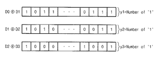
座標点CP1(x1、y1)を求めるためには読み取り電圧R0、R1によるそれぞれの読み取り動作が行われる。読み取り電圧R0によって選択されたメモリセルが読み取られ、読み取られたデータはバイナリの論理値として保存される。例えば、しきい値電圧が読み取り電圧R0よりも低いメモリセルから読み取られたデータは論理‘1’にラッチされる。一方、しきい値電圧が読み取り電圧R0よりも高いメモリセルから読み取られたデータは論理‘0’にラッチされる。選択されたメモリセルのうちしきい値電圧が読み取り電圧R0よりも高く、読み取り電圧R1よりも低いメモリセルは読み取り電圧R0によってオフセル(Off cell)に、読み取り電圧R1によってオンセル(On cell)に検出される。したがって、読み取り電圧R0によって読み出されたデータD0と読み取り電圧R1によって読み出されたデータD1に対する同じ列同士の排他的論理和(XOR)を実行すると、電圧帯域ΔV1に対応するメモリセルの数を求めることができる。 In order to obtain the coordinate point CP1 (x1, y1), the respective reading operations with the reading voltages R0 and R1 are performed. The memory cell selected by the read voltage R0 is read, and the read data is stored as a binary logical value. For example, data read from a memory cell whose threshold voltage is lower than the read voltage R0 is latched to logic '1'. On the other hand, data read from a memory cell having a threshold voltage higher than the read voltage R0 is latched to logic '0'. Among the selected memory cells, a memory cell having a threshold voltage higher than the read voltage R0 and lower than the read voltage R1 is detected as an off cell by the read voltage R0 and detected as an on cell by the read voltage R1. Is done. Therefore, when an exclusive OR (XOR) between the same columns is performed on the data D0 read by the read voltage R0 and the data D1 read by the read voltage R1, the number of memory cells corresponding to the voltage band ΔV1 is calculated. Can be sought.
しきい値電圧が電圧帯域ΔV1に位置するメモリセルの数はビットカウンタ112(図1参照)によってカウントされる。このとき、座標点CP1の座標値x1は読み取り電圧R0、R1の中央値(Median)にマッピングする。即ち、座標値x1は(R0+R1)/2にマッピングすることができる。そして、座標点CP1の座標値y1はしきい値電圧が電圧帯域ΔV1に分布するメモリセルの数にマッピングする。 The number of memory cells whose threshold voltage is located in the voltage band ΔV1 is counted by the bit counter 112 (see FIG. 1). At this time, the coordinate value x1 of the coordinate point CP1 is mapped to the median value (Median) of the read voltages R0 and R1. That is, the coordinate value x1 can be mapped to (R0 + R1) / 2. The coordinate value y1 of the coordinate point CP1 is mapped to the number of memory cells whose threshold voltage is distributed in the voltage band ΔV1.
座標点CP2(x2、y2)を求めるためには読み取り電圧R1、R2によるそれぞれの読み取り動作が必要である。読み取り電圧R1によって読み出されたデータD1と読み取り電圧R2によって読み出されたデータD2に対する排他的論理和(XOR)を実行すると、しきい値電圧が電圧帯域ΔV2に分布するメモリセルの数を求めることができる。このように求められた電圧帯域ΔV2に対応するメモリセルの数は座標値y2にマッピングする。そして、座標点CP2の座標値x2は読み取り電圧R1、R2の中間値(または、平均値)にマッピングする。即ち、座標値x2は(R1+R2)/2に設定することができる。 In order to obtain the coordinate point CP2 (x2, y2), each reading operation with the reading voltages R1 and R2 is necessary. When exclusive OR (XOR) is performed on the data D1 read by the read voltage R1 and the data D2 read by the read voltage R2, the number of memory cells in which the threshold voltage is distributed in the voltage band ΔV2 is obtained. be able to. The number of memory cells corresponding to the voltage band ΔV2 thus determined is mapped to the coordinate value y2. The coordinate value x2 of the coordinate point CP2 is mapped to the intermediate value (or average value) of the read voltages R1 and R2. That is, the coordinate value x2 can be set to (R1 + R2) / 2.
座標点CP3(x3、y3)を求めるためには読み取り電圧R2、R3によるそれぞれの読み取り動作が先行される。読み取り電圧R2によって読み出されたデータD2と読み取り電圧R3によって読み出されたデータD3に対する排他的論理和(XOR)を実行すると、しきい値電圧が電圧帯域ΔV3に分布するメモリセルの数を求めることができる。このように求められた電圧帯域ΔV3に対応するメモリセルの数は座標値y3にマッピングする。そして、座標点CP3の座標値x3は読み取り電圧R2、R3の中間値(または、平均値)にマッピングする。即ち、座標値x3は(R2+R3)/2に設定することができる。 In order to obtain the coordinate point CP3 (x3, y3), each reading operation with the reading voltages R2 and R3 is preceded. When an exclusive OR (XOR) is performed on the data D2 read by the read voltage R2 and the data D3 read by the read voltage R3, the number of memory cells in which the threshold voltage is distributed in the voltage band ΔV3 is obtained. be able to. The number of memory cells corresponding to the voltage band ΔV3 thus determined is mapped to the coordinate value y3. The coordinate value x3 of the coordinate point CP3 is mapped to the intermediate value (or average value) of the read voltages R2 and R3. That is, the coordinate value x3 can be set to (R2 + R3) / 2.
ここで、読み取り電圧R0、R1、R2、R3のそれぞれの間隔に対応する電圧帯域ΔV1、ΔV2、ΔV3は同一または互いに異なる値で提供される。電圧帯域ΔV1、ΔV2、ΔV3の大きさが同様に提供されるときは読み取り電圧R0から一定の電圧間隔で順に増加する読み取り電圧が提供される。したがって、読み取り電圧の生成が容易である。例えば、1つの読み取り電圧R0のみを参照して読み取り電圧R1、R2、R3を生成する場合は、増加分ΔV1、ΔV2、ΔV3を同じ値に設定すればよい。 Here, the voltage bands ΔV1, ΔV2, and ΔV3 corresponding to the intervals of the read voltages R0, R1, R2, and R3 are provided with the same or different values. When the magnitudes of the voltage bands ΔV1, ΔV2, and ΔV3 are provided in the same manner, read voltages that sequentially increase from the read voltage R0 at a constant voltage interval are provided. Therefore, it is easy to generate a read voltage. For example, when the read voltages R1, R2, and R3 are generated by referring to only one read voltage R0, the increments ΔV1, ΔV2, and ΔV3 may be set to the same value.
以上から、分布谷140に対応する確率密度関数を2次関数でモデル化するための3つの座標値を求める過程が説明された。座標値が求められると、その後は連立多項式を構成し、連立多項式に座標値を代入して確率密度関数の係数を求める。そして、確率密度関数に対する最小値に対応するしきい値電圧が最適な読み取り電圧に決定される。
From the above, the process of obtaining three coordinate values for modeling the probability density function corresponding to the
図6A及び図6Bは3次関数でモデル化される確率密度関数の分布谷を示すグラフである。図6Aは分布谷130の曲線C2上の座標点を示し、図6Bは、曲線C2上の座標値を求めるための読み取り方法を示すグラフである。
6A and 6B are graphs showing distribution valleys of a probability density function modeled by a cubic function. 6A shows a coordinate point on the curve C2 of the
図6Aを参照すると、しきい値電圧に対するメモリセルの確率密度関数の分布谷130は曲線C2のような3次関数でモデル化することができる。曲線C2に対応する関数の場合には変曲点(Inflection point)が存在する3次関数の形で図示できる。消去状態E0に含まれるメモリセルが広い電圧範囲に分布する。一方、プログラムの状態P1に含まれるメモリセルは相対的にISPP(Incremental Step Pulse Programming)のようなプログラム方法によってより狭い電圧範囲で管理される。このような管理方法によって、消去状態E0とプログラム状態P1との間の分布谷130は3次曲線でモデルすることができる。
Referring to FIG. 6A, the
分布谷に対応する曲線C2の最小点を求めるためには3次連立方程式を利用して演算する。分布谷に対応する曲線C2に対応する3次関数の係数を求めるためには少なくとも4つの座標点CP1、CP2、CP3、CP4の座標値が必要である。4つの座標点CP1、CP2、CP3、CP4は互いに異なる座標点であれば4次連立方程式の解を求めることができる。 In order to obtain the minimum point of the curve C2 corresponding to the distribution valley, calculation is performed using a cubic simultaneous equation. In order to obtain the coefficient of the cubic function corresponding to the curve C2 corresponding to the distribution valley, the coordinate values of at least four coordinate points CP1, CP2, CP3, CP4 are necessary. If the four coordinate points CP1, CP2, CP3, CP4 are different from each other, the solution of the fourth order simultaneous equation can be obtained.
座標点は図示のようにCP1(x1、y1)、CP2(x2、y2)、CP3(x3、y3)、CP4(x4、y4)になる。3次関数(y=a0+a1x+a2x2+a3x3)の係数を求めるための連立方程式は次の数式5で表すことができる。
The coordinate points are CP1 (x1, y1), CP2 (x2, y2), CP3 (x3, y3), CP4 (x4, y4) as shown in the figure. Simultaneous equations for determining the coefficients of the
ここで、ε1、ε2、ε3、ε4はそれぞれの座標点に対応するDCオフセットやエラーと見なす。しかし、最小値を求めるための関数の微分によって消去される項目である。 Here, ε1, ε2, ε3, and ε4 are regarded as DC offsets and errors corresponding to the respective coordinate points. However, it is an item that is eliminated by differentiation of the function for obtaining the minimum value.
数式5にそれぞれの座標値を代入して連立方程式を演算すると分布谷130に対応する曲線C2の3次関数の係数a0、a1、a2、a3が求められる。その後に係数a0、a1、a2、a3を有する3次関数を微分した値が0になる根Xoptは次の数式6で表すことができる。
When the simultaneous equations are calculated by substituting the respective coordinate values into Equation 5, coefficients a0, a1, a2, and a3 of the cubic function corresponding to the
ここで、係数a3が正数である場合、3次関数の微分値が0となる解は2つの実根で表す。2つの実根の中で極小点(Relative minimum point)に対応する値が求めようとする値である。したがって、数式6で2つの実根の中で大きな値が最適な読み取り電圧Xoptとなる。係数a3が負数である場合、2つの実根の中で小さな値が最適な読み取り電圧Xoptとなる。この場合、以下の数式7に最適な読み取り電圧Xoptを表すことができる。 Here, when the coefficient a3 is a positive number, a solution in which the differential value of the cubic function is 0 is represented by two real roots. Among the two real roots, a value corresponding to a local minimum point is a value to be obtained. Therefore, in Formula 6, a large value among the two real roots is the optimum read voltage Xopt. When the coefficient a3 is a negative number, a small value among the two real roots is the optimum read voltage Xopt. In this case, the optimum read voltage Xopt can be expressed by the following formula 7.
図6Bは図6Aの曲線C2からの座標点を求めるための方法を示すグラフである。図6Bを参照すると、曲線C2を3次関数で回帰分析するために少なくとも4つの座標点が求められる。即ち、3次関数で回帰分析をするために、メモリセルに対して少なくとも5回の読み取り動作が先行される。それぞれの読み取り動作から提供される読み取り電圧(Ri、iは0<=i<=4の整数)は異なっている。 FIG. 6B is a graph showing a method for obtaining coordinate points from the curve C2 of FIG. 6A. Referring to FIG. 6B, at least four coordinate points are obtained for regression analysis of the curve C2 with a cubic function. That is, in order to perform regression analysis with a cubic function, at least five read operations are preceded by the memory cell. The read voltage (Ri, i is an integer of 0 <= i <= 4) provided from each read operation is different.
座標点CP1(x1、y1)を求めるためには読み取り電圧R0、R1による読み取り動作が行われる。読み取り電圧R0によってデータD0が選択されたメモリセルから検出される。そして、読み取り電圧R1によってデータD1が選択されたメモリセルから検出される。データD0とデータD1の排他的論理和演算を実行して、論理‘1’の数をカウントすると読み取り電圧R0、R1の間(電圧帯域ΔV1)に対応するメモリセルの数が求められる。このとき、座標点CP1の座標値x1は読み取り電圧R0、R1の中央値(Median)にマッピングする。即ち、座標値x1は(R0+R1)/2にマッピングすることができる。そして、座標点CP1の座標値y1は電圧帯域ΔV1にしきい値電圧が分布するメモリセルの数にマッピングされる。 In order to obtain the coordinate point CP1 (x1, y1), a reading operation with the reading voltages R0 and R1 is performed. The data D0 is detected from the selected memory cell by the read voltage R0. Then, the data D1 is detected from the selected memory cell by the read voltage R1. When the exclusive OR operation of the data D0 and the data D1 is executed and the number of logic ‘1’ is counted, the number of memory cells corresponding to between the read voltages R0 and R1 (voltage band ΔV1) is obtained. At this time, the coordinate value x1 of the coordinate point CP1 is mapped to the median value (Median) of the read voltages R0 and R1. That is, the coordinate value x1 can be mapped to (R0 + R1) / 2. The coordinate value y1 of the coordinate point CP1 is mapped to the number of memory cells in which the threshold voltage is distributed in the voltage band ΔV1.
座標点CP2(x2、y2)を求めるためには読み取り電圧R1、R2によるそれぞれの読み取り動作が行われる。読み取り電圧R1によって読み出されたデータD1と読み取り電圧R2によって読み出されたデータD2に対する排他的論理和(XOR)を実行すると、しきい値電圧が電圧帯域ΔV2に分布するメモリセルの数を求めることができる。このように求められた電圧帯域ΔV2に対応するメモリセルの数は座標値y2にマッピングする。そして、座標点CP2の座標値x2は読み取り電圧R1、R2の中央値(Median)にマッピングすることができる。つまり、座標値x2は(R1+R2)/2に設定することができる。 In order to obtain the coordinate point CP2 (x2, y2), each reading operation with the reading voltages R1 and R2 is performed. When exclusive OR (XOR) is performed on the data D1 read by the read voltage R1 and the data D2 read by the read voltage R2, the number of memory cells in which the threshold voltage is distributed in the voltage band ΔV2 is obtained. be able to. The number of memory cells corresponding to the voltage band ΔV2 thus determined is mapped to the coordinate value y2. The coordinate value x2 of the coordinate point CP2 can be mapped to the median value of the read voltages R1 and R2. That is, the coordinate value x2 can be set to (R1 + R2) / 2.
座標点CP3(x3、y3)を求めるためには読み取り電圧R2、R3によるそれぞれの読み取り動作が行われる。読み取り電圧R2によって読み出されたデータD2と読み取り電圧R3によって読み出されたデータD3に対する排他的論理和(XOR)を実行すると、しきい値電圧が電圧帯域ΔV3に分布するメモリセルの数を求めることができる。このように求められた電圧帯域ΔV3に対応するメモリセルの数は座標値y3にマッピングする。そして、座標点CP3の座標値x3は読み取り電圧R2、R3の中央値(Median)にマッピングする。つまり、座標値x3は(R2+R3)/2に設定することができる。 In order to obtain the coordinate point CP3 (x3, y3), the respective reading operations with the reading voltages R2 and R3 are performed. When an exclusive OR (XOR) is performed on the data D2 read by the read voltage R2 and the data D3 read by the read voltage R3, the number of memory cells in which the threshold voltage is distributed in the voltage band ΔV3 is obtained. be able to. The number of memory cells corresponding to the voltage band ΔV3 thus determined is mapped to the coordinate value y3. Then, the coordinate value x3 of the coordinate point CP3 is mapped to the median value (Median) of the read voltages R2 and R3. That is, the coordinate value x3 can be set to (R2 + R3) / 2.
座標点CP4(x4、y4)を求めるためには、読み取り電圧R3、R4によるそれぞれの読み取り動作が行われる。読み取り電圧R3によって読み出されたデータD3と読み取り電圧R4によって読み出されたデータD4に対する排他的論理和(XOR)を実行すると、しきい値電圧が電圧帯域ΔV4に分布するメモリセルの数を求めることができる。このように求められた電圧帯域ΔV4に対応するメモリセルの数は座標値y4にマッピングする。そして、座標点CP4の座標値x4は読み取り電圧R3、R4の中央値(Median)にマッピングする。つまり、座標値x4は(R3+R4)/2に設定することができる。 In order to obtain the coordinate point CP4 (x4, y4), each reading operation with the reading voltages R3 and R4 is performed. When exclusive OR (XOR) is performed on the data D3 read by the read voltage R3 and the data D4 read by the read voltage R4, the number of memory cells in which the threshold voltage is distributed in the voltage band ΔV4 is obtained. be able to. The number of memory cells corresponding to the voltage band ΔV4 thus determined is mapped to the coordinate value y4. Then, the coordinate value x4 of the coordinate point CP4 is mapped to the median value (Median) of the read voltages R3 and R4. That is, the coordinate value x4 can be set to (R3 + R4) / 2.
ここで、読み取り電圧R0、R1、R2、R3、R4のそれぞれの増加分ΔV1、ΔV2、ΔV3、ΔV4は同一または異なる値で提供される。ただし、読み取り電圧の増加分が同様に提供されるときは、読み取り電圧R0に対して一定の電圧だけ順に増加する電圧で生成される。例えば、1つの読み取り電圧R0のみを参照して読み取り電圧R1、R2、R3、R4を生成する場合は増加分ΔV1、ΔV2、ΔV3、ΔV4を同じ値に設定すればよい。 Here, the increments ΔV1, ΔV2, ΔV3, and ΔV4 of the read voltages R0, R1, R2, R3, and R4 are provided with the same or different values. However, when an increase in the read voltage is provided in the same manner, the read voltage is generated with a voltage that sequentially increases by a certain voltage with respect to the read voltage R0. For example, when the read voltages R1, R2, R3, and R4 are generated with reference to only one read voltage R0, the increments ΔV1, ΔV2, ΔV3, and ΔV4 may be set to the same value.
以上から、分布谷に対応する確率密度関数が3次関数に対応する曲線C2でモデル化され、回帰分析法を適用するための座標値のCP1、CP2、CP3、CP4を求める過程が説明された。座標値が求められると、その後には回帰分析法を適用して3次関数の極小値に対応する電圧を最適な読み取り電圧に決定する。 From the above, the process of calculating the probability values corresponding to the distribution valleys with the curve C2 corresponding to the cubic function and obtaining the coordinate values CP1, CP2, CP3, and CP4 for applying the regression analysis method has been described. . When the coordinate value is obtained, a regression analysis method is applied thereafter to determine a voltage corresponding to the minimum value of the cubic function as an optimum reading voltage.
図7は本発明の一実施形態によるメモリシステムの動作を示す図である。図7を参照すると、メモリコントローラ110と不揮発性メモリ装置120は座標値を求めるための読み取り電圧のそれぞれに対応するリードコマンドとデータを交換する。
FIG. 7 is a diagram illustrating an operation of the memory system according to the embodiment of the present invention. Referring to FIG. 7, the
メモリコントローラ110は分布谷に対応する確率密度関数の座標点を求めるためのリードコマンドを不揮発性メモリ装置120に伝達する。このとき、メモリコントローラ110は回帰分析法を適用するために選択されたメモリセルに対して読み取り電圧R0で読み込むようにコマンドを提供する。これにより、不揮発性メモリ装置120は読み取り電圧R0を生成して選択されたメモリセルを検出する。そして、不揮発性メモリ装置120は読み取り電圧R0によって検出されたデータD0をメモリコントローラ110に出力する。
The
続いて、メモリコントローラ110は選択されたメモリセルを読み取り電圧R0より高い読み取り電圧R1で読み込むようにリードコマンドを提供する。リードコマンドに応答して不揮発性メモリ装置120は読み取り電圧R1に対応する電圧を生成し、選択されたメモリセルを検出する。そして、不揮発性メモリ装置120は読み取り電圧R1によって検出及びラッチされたデータD1をメモリコントローラ110に出力する。
Subsequently, the
このように、メモリコントローラ110には不揮発性メモリ装置120から選択されたメモリセルに対する読み取り電圧R0〜Rn−1によって読み取られたデータD0〜Dn−1が提供される。座標点を求めるための読み取り動作が完了すると、メモリコントローラ110は分布谷に対応する確率密度関数(PDF)を求め、確率密度関数の最小値または極小値を求める演算を実行する。そして、最小値に対応するしきい値電圧のレベルを2つの状態を識別するための読み取り電圧に決定する。これらの手順は段階S10で示されている。
As described above, the
図8は不揮発性メモリ装置から提供されるデータを示す図である。図8を参照すると、選択されたメモリセルに対する読み取り電圧R0〜Rn−1のそれぞれによって読み取られたデータD0〜D3が例示的に示されている。 FIG. 8 is a diagram illustrating data provided from the nonvolatile memory device. Referring to FIG. 8, data D0 to D3 read by read voltages R0 to Rn-1 for a selected memory cell are exemplarily shown.
不揮発性メモリ装置120はメモリコントローラ110のコマンドに応答して読み取り電圧R0によって読み取られたデータD0を出力する。そして、不揮発性メモリ装置120はメモリコントローラ110のコマンドに応答して読み取り電圧R1によって読み取られたデータD1を出力する。同様に、不揮発性メモリ装置120はメモリコントローラ110のコマンドに応じて読み取り電圧R2によって読み取られたデータD2と読み取り電圧R3によって読み取られたデータD3を出力する。
The
互いに異なる読み取り電圧によって読み取られたデータD0、D1、D2、D3が出力されると、メモリコントローラ110のビットカウンタ112によって排他的論理和(XOR)演算が実行される。データ間の排他的論理和演算は同じ列同士に適用される。ビットカウンタ112はデータD0とデータD1に対する排他的論理和演算の結果に含まれる論理‘1’の数をカウントして座標値y1に決定する。そして、読み取り電圧R0、R1の中間値(または平均値)を座標値x1に決定する。
When data D0, D1, D2, and D3 read at different read voltages are output, an exclusive OR (XOR) operation is performed by the bit counter 112 of the
上述した方法でデータD1、D2の排他的論理和演算を通じて座標値x2、y2を求めることができる。同様に、データD2、D3の排他的論理和演算を通じて座標値x3、y3を求める。3つの座標点の座標値が決定されると、2次関数でモデル化される分布谷関数の回帰分析法を適用するための諸情報は確保される。 The coordinate values x2 and y2 can be obtained through the exclusive OR operation of the data D1 and D2 by the method described above. Similarly, coordinate values x3 and y3 are obtained through exclusive OR operation of data D2 and D3. When the coordinate values of the three coordinate points are determined, various information for applying the regression analysis method of the distribution valley function modeled by the quadratic function is secured.
図9は、本発明の実施形態による読み取りレベルを決定する方法を示すフローチャートである。図1及び9を参照して、分布谷を確率密度関数(PDF)でモデル化し、モデル化した確率密度関数から最適な読み取り電圧を決定するための手順が説明される。 FIG. 9 is a flowchart illustrating a method for determining a read level according to an embodiment of the present invention. With reference to FIGS. 1 and 9, a procedure for modeling a distribution valley with a probability density function (PDF) and determining an optimum read voltage from the modeled probability density function will be described.
S110段階では、メモリコントローラ110は不揮発性メモリ装置120に複数の読み取り電圧R0〜Rn−1のレベル情報を含むリードコマンドを提供する。不揮発性メモリ装置120は読み取り電圧R0〜Rn−1のそれぞれによって読み取られたデータD0〜Dn−1をメモリコントローラ110に伝達する。
In operation S110, the
S120段階では、メモリコントローラ110は伝達されたデータD0〜Dn−1を参照して座標値を計算する。例えば、メモリコントローラ110はそれぞれの読み取り電圧の間に対応するしきい値電圧を有するメモリセルの数をカウントする。メモリコントローラ110はカウント結果に基づいて少なくとも3つの座標点の座標値を決定する。
In step S120, the
S130段階では、メモリコントローラ110の回帰分析器114は座標値を参照して分布谷に対応する確率密度関数を求める。即ち、回帰分析器114は座標値を参照して確率密度関数の係数を求める。確率密度関数を求めるために回帰分析器114は、2次連立方程式または3次連立方程式を使用することができる。
In step S130, the
S140段階では、回帰分析器114は確率密度関数から最小値または極小値に対応するしきい値電圧レベルを求める。例えば、2次関数でモデル化される確率密度関数の場合は1つの最小値に対応するしきい値電圧レベルを求めることによって最適な読み取り電圧Voptを決定することになる。一方、3次関数でモデル化される場合には確率密度関数(PDF)の微分値を0とする実根は2つ存在する。即ち、2つの実根のうち1つは極大値に対応し、残りの1つは極小値に対応する。
In step S140, the
S150段階では、メモリコントローラ110は分布谷に対応する確率分布関数(PDF)の微分値が0となるしきい値電圧のうちいずれかを最適な読み取り電圧に選択する。2次関数でモデル化された確率密度関数(PDF)の場合にはその微分値を0とする根は1つだけ存在する。一方、3次関数でモデル化された確率密度関数の場合、最大2つの実根が存在する。しかし、消去状態E0とプログラム状態P1との間の分布谷の形は3次関数の極小値(a3>0のとき)周辺の曲線形態と類似である。したがって、2つの実根のうち極小点に対応する1つを最適な読み取り電圧に選択することは妥当である。したがって、2つの実根のうち大きさがもっと大きい実根の方が最適な読み取り電圧Voptに選択される。
In step S150, the
以上では、不揮発性メモリ装置120の読み取り電圧を調整するために使用される回帰分析法を説明した。回帰分析を実行するためにモデル化される確率密度関数(PDF)の座標値を求める。2次関数で確率密度関数(PDF)をモデル化する場合には少なくとも3つの座標値が必要である。このように、3つの座標値を得るためには互いに異なる読み取り電圧を適用する少なくとも4回の読み取り動作が行なわれる。3次関数で確率密度関数(PDF)をモデル化する場合には少なくとも4つの座標値が必要である。このように、4つの座標値を得るためには互いに異なる読み取り電圧を適用する少なくとも5回の読み取り動作が行なわれる。
The regression analysis method used to adjust the read voltage of the
このような回帰分析法によると、最小限の読み取り動作を通じて分布谷に対応する確率密度関数(PDF)をモデル化することができる。そして、モデル化された確率密度関数の最小値または極小値に対応するしきい値電圧をメモリセルの読み取り電圧に決定することができる。この方式の読み取り電圧調整は最小限の読み取り動作を必要とするため、パフォーマンスの向上を可能にする。なお、分布谷に最も近似する形態の確率密度関数(PDF)でモデル化が可能なので高精度の最小点の検出が可能である。したがって、本発明の回帰分析法を通じて調整された読み取り電圧を使用する場合、高いデータの信頼性(Data Integrity)が期待される。 According to such a regression analysis method, a probability density function (PDF) corresponding to a distribution valley can be modeled through a minimum reading operation. Then, the threshold voltage corresponding to the minimum value or the minimum value of the modeled probability density function can be determined as the read voltage of the memory cell. Since this method of read voltage adjustment requires a minimum read operation, performance can be improved. Since modeling can be performed with a probability density function (PDF) in a form that most closely approximates the distribution valley, the minimum point can be detected with high accuracy. Therefore, when using the read voltage adjusted through the regression analysis method of the present invention, high data integrity is expected.
図10は本発明の他の実施形態によるメモリシステムの読み取り方法を示す図である。図10を参照すると、メモリコントローラ110(図1参照)のリードコマンドに応答して不揮発性メモリ装置120(図1参照)は検出されたデータに対する排他的論理和(XOR)演算を実行して出力する。 FIG. 10 is a diagram illustrating a reading method of a memory system according to another embodiment of the present invention. Referring to FIG. 10, in response to a read command from the memory controller 110 (see FIG. 1), the nonvolatile memory device 120 (see FIG. 1) performs an exclusive OR (XOR) operation on the detected data and outputs it. To do.
回帰分析を適用するために、メモリコントローラ110は不揮発性メモリ装置120へ読み取りレベルの情報を含むリードコマンドを送信する。特に、メモリコントローラ110は1つの読み取り電圧に対応するデータを要求するものではなく、複数の読み取り電圧情報をリードコマンドの段階で不揮発性メモリ装置120に伝送する。即ち、メモリコントローラ110はリードコマンドの段階で複数の読み取り電圧R0、R1、R2、...、Rnを指定することができる。
In order to apply the regression analysis, the
メモリコントローラ110のリードコマンドに応答して不揮発性メモリ装置120は順に選択されたメモリセルを検出する。不揮発性メモリ装置120は読み取り電圧R0を選択されたメモリセルのワード線に提供してメモリセルを検出する。読み取り電圧R0によって検出されたデータD0はページバッファ123(図2参照)に備えられるラッチに保存される。続いて、不揮発性メモリ装置120は読み取り電圧R1を選択されたメモリセルのワード線に提供してメモリセルを検出する。読み取り電圧R1によって検出されたデータD1はページバッファ123に備えられるラッチに保存される。不揮発性メモリ装置120は互いに異なる読み取り電圧によって検出されたデータD0、D1に対する排他的論理和(XOR)演算を実行する。そして、不揮発性メモリ装置120はその結果をメモリコントローラ110に伝達する。
In response to the read command of the
不揮発性メモリ装置120は複数の読み取り電圧R0、R1、R2、...、Rnを順に適用して選択されたメモリセルを検出し、検出されたデータをラッチする。これらの検出及びラッチ動作は排他的論理和演算(XOR)及びその結果を出力する動作と重畳して実行される。複数の読み取り電圧によって検出されたデータは少なくとも2つのページサイズのラッチに順に保存されると、保存されたデータの同じ列同士に排他的論理和演算が実行される。そして、その排他的論理和(XOR)演算の結果は入出力バッファ124によって外部に出力される。これらの手順によって読み取り電圧R1、R2に対応するデータD0、D1に対する排他的論理和(XOR)の結果が出力される。そして、読み取り電圧R2、R3に対応するデータD2、D3に対する排他的論理和(XOR)の結果が連続して出力される。4つの読み取りレベルが指定されると、排他的論理和(XOR)演算の結果は3回の読み取りの単位(例えば、ページ)でメモリコントローラ110に伝送される。
The
メモリコントローラ110はデータのD0〜Dnの排他的論理和(XOR)演算の結果を受信する。そして、受信されたそれぞれの排他的論理和の結果を参照して、読み取り電圧の間に分布するメモリセルの数をカウントする。即ち、メモリコントローラ110のビットカウンタ112は排他的論理和(XOR)の結果に含まれる論理‘1’の数をカウントする。カウント動作が完了すると、複数の座標点のそれぞれの座標値が決定される。そして、メモリコントローラ110は決定された座標値を参照して分布谷の形に対応する確率密度関数を求めるようになる。メモリコントローラ110の回帰分析器114は確率密度関数の最小値または極小値を求め、それに対応するしきい値電圧のレベルを新しい読み取り電圧に決定する。このような処理段階がS20に示されている。
The
ここで、リードコマンドを提供している段階で、最初の読み取り操作のための読み取り電圧R0と後に提供される読み取り電圧との電圧差についての情報が提供される。即ち、最初に提供される読み取り電圧R0と順に提供される電圧の間のオフセット情報がさらに提供される。不揮発性メモリ装置120はオフセット情報を参照して順に読み取り電圧を生成し、選択されたメモリセルを検出する。
Here, when the read command is provided, information about the voltage difference between the read voltage R0 for the first read operation and the read voltage provided later is provided. That is, offset information between the read voltage R0 provided first and the voltages provided in order is further provided. The
連続して読み取られたデータ間の排他的論理和(XOR)演算を実行して出力する場合に、メモリコントローラ110の演算負担を減らすことができる。そして、読み取りデータを出力する場合より不揮発性メモリ装置120の出力回数も減らすことができる。
When an exclusive OR (XOR) operation between continuously read data is executed and output, the operation load on the
図11は図10の排他的論理和演算の結果を例示的に示す図である。図11を参照すると、不揮発性メモリ装置120はメモリコントローラ110のコマンドに基づいて2つの読み取りレベルに応じて検出されたデータを排他的論理和(XOR)演算を実行した後に出力する。
FIG. 11 is a diagram exemplarily showing the result of the exclusive OR operation of FIG. Referring to FIG. 11, the
不揮発性メモリ装置120は選択されたメモリセルをメモリコントローラ110から提供された読み取り電圧を参照して順次検出する。不揮発性メモリ装置120は読み取り電圧R0によって読み取られたデータD0を第1ラッチに保存する。続いて、不揮発性メモリ装置120は読み取り電圧R1によって読み取られたデータD1を第2ラッチに保存する。ここで、第1ラッチと第2ラッチはページバッファ123に備えられるラッチである。そして、1つの読み取りレベルによって読み取られたデータは1つのページ単位と仮定する。第1ラッチと第2ラッチに保存されたデータD0、D1を同じ列同士で排他的論理和(XOR)を実行すると、1つのページサイズで出力される。そして、排他的論理和(XOR)演算の結果のデータがメモリコントローラ110に伝送されると、ビットカウンタ112は伝送されたデータに含まれる論理‘1’の数をカウントする。排他的論理和(XOR)の結果データに含まれる論理‘1’の数が座標値y1にマッピングされる。そして、座標値x1は読み取り電圧R0、R1の平均値にマッピングされる。
The
上述したように不揮発性メモリ装置120は読み取り電圧R1によって読み取られたデータD1と読み取り電圧R2によって読み取られたデータD2を処理してメモリコントローラ110に提供する。これにより、提供されたデータからビットカウンタ112は論理‘1’の数をカウントし、カウントされた値は座標値y2にマッピングされる。そして、不揮発性メモリ装置120は読み取り電圧R2によって読み取られたデータD2と読み取り電圧R3によって読み取られたデータD3を処理してメモリコントローラ110に提供する。これにより、メモリコントローラ110は座標値y3を決定する。
As described above, the
以上の方法によれば、メモリコントローラ110と不揮発性メモリ装置120との間で発生するトランザクションの数を減らすことができる。したがって、排他的論理和演算せずにデータがメモリコントローラ110に伝送される実施形態に比べてパフォーマンスの向上を期待することができる。
According to the above method, the number of transactions that occur between the
図12は本発明の他の実施形態によるメモリシステムを示すブロック図である。図12を参照すると、メモリシステム200はメモリコントローラ210と不揮発性メモリ装置220を備える。メモリコントローラ210は不揮発性メモリ装置220から提供される読み取り結果を参照して回帰分析を行なって最適な読み取り電圧を決定する。より詳細に説明すると、メモリコントローラ210は読み取りレベルの調整が必要な状況では読み取り電圧Rn−1、Rnの情報を含むリードコマンドを不揮発性メモリ装置220に提供する。例えば、メモリコントローラ110はリードコマンドを提供するとき、互いに異なるレベルRn−1、Rnで選択されたメモリセルを検出するためのコマンドを提供する。このとき、不揮発性メモリ装置220はコマンドに応答して互いに異なるレベルRn−1、Rnに連続して検出されたデータDn−1、Dn間の排他的論理和(XOR)演算を実行する。そして、不揮発性メモリ装置220は排他的論理和演算の結果データに含まれる論理‘1’の数をカウントする。このカウント動作は不揮発性メモリ装置220内に備えられているビットカウンタ227によって行われる。そして、不揮発性メモリ装置220はカウントされた値を読み取り電圧の平均値に対応する座標値ynで出力する。
FIG. 12 is a block diagram illustrating a memory system according to another embodiment of the present invention. Referring to FIG. 12, the
メモリコントローラ210は不揮発性メモリ装置220から提供される座標値ynを要求する。例えば、少なくとも3つの異なる座標値が必要な場合、互いに異なるしきい値電圧帯域に含まれるメモリセルの数をカウントするためのコマンドを3回提供する。それぞれのコマンドに応答して出力される座標値を参照してメモリコントローラ210は分布谷に対応する確率密度関数(PDF)を求める。そして、確率密度関数(PDF)から最小値または極小値を求め、最適な読み取り電圧を決定する動作は回帰分析器214から行われる。
The
上述した実施形態によれば、メモリコントローラ210は不揮発性メモリ装置220から座標値ynを直接取得することができる。このように、メモリコントローラ210が実行する操作の負担を不揮発性メモリ装置220と分担することができる。本発明のメモリコントローラ210は回帰分析法を使用して不揮発性メモリ装置220に対する最小限のアクセスによっても最適な読み取り電圧を決定することができる。したがって、読み取り電圧のレベルを調整するための操作にかかる時間を最小限に抑えることができる。
According to the above-described embodiment, the
図13は図12に示された不揮発性メモリ装置の構成を例示的に示すブロック図である。図13を参照すると、不揮発性メモリ装置220はセルアレイ221、行デコーダ222、ページバッファ223、入出力バッファ224、制御ロジック225、電圧発生器226そして、ビットカウンタ227を備える。不揮発性メモリ装置220はビットカウンタ227の構成を除けば図2の構成と同じである。従って、セルアレイ221、行デコーダ222、ページバッファ223、入出力バッファ224、制御ロジック225、電圧発生器226の説明は省略する。
FIG. 13 is a block diagram exemplarily showing a configuration of the nonvolatile memory device shown in FIG. Referring to FIG. 13, the
不揮発性メモリ装置220はメモリコントローラ210によって選択されたメモリセルから少なくとも2つの読み取り電圧による読み取りを実行し、1つの座標値を出力するように制御される。メモリコントローラ210からコマンドが提供されると不揮発性メモリ装置220は選択されたメモリセルから少なくとも2つの読み取り電圧Ri−1、Riを使用してデータを検出する。検出されたデータはページバッファ223に順に保存される。その後、ビットカウンタ227はページバッファ223に保存された2つのページのデータに対する排他的論理和(XOR)演算を実行する。そして、ビットカウンタ227はその結果に含まれる論理‘1’の数をカウントする。ビットカウンタ227はカウント結果yiを入出力バッファ224に伝達し、入出力バッファ224はメモリコントローラ210にカウント結果yiを出力する。
The
上述した機能のためにビットカウンタ227は少なくとも2つのページを保存するためのラッチ(またはレジスタ)と排他的論理和(XOR)演算を実行するための論理ゲートの列を含む。例えば、ビットカウンタ227は互いに異なる読み取り電圧で読み出された2つのページを備えられたラッチに保存することができます。そして、ビットカウンタ227は同じ列に対応するビット間に対する排他的論理和(XOR)演算を実行する論理ゲートの列を備える。なお、ビットカウンタ227は論理ゲートの列から出力されるページサイズのデータに含まれる論理‘1’の数をカウントするカウンタ回路(図示せず)を備える。カウンタ回路の出力が対応する読み取りレベルの座標値yiになる。
For the functions described above,
図14は図12のメモリシステムのまた他の読み取り方法を示す図である。図14を参照すると、メモリコントローラ210(図12参照)のリードコマンドに応答して不揮発性メモリ装置220(図12参照)は複数の座標値yi(1<=i<=n)を提供する。 FIG. 14 is a diagram showing still another reading method of the memory system of FIG. Referring to FIG. 14, in response to a read command from the memory controller 210 (see FIG. 12), the nonvolatile memory device 220 (see FIG. 12) provides a plurality of coordinate values yi (1 <= i <= n).
メモリコントローラ210は読み取りレベルを調整するためのリードコマンド(Read CMD)を不揮発性メモリ装置220に提供するとき、すべての読み取り電圧R0〜Rnを指定する。図面のR0、Rnは読み取り電圧R0から読み取り電圧Rnまでのすべての読み取り電圧を意味する。
When the
メモリコントローラ210のリードコマンドに応答して不揮発性メモリ装置220は順に選択されたメモリセルを検出する。不揮発性メモリ装置220は読み取り電圧R0を選択されたメモリセルのワード線に提供してメモリセルを検出する。読み取り電圧R0によって検出されたデータD0はページバッファ223(図13参照)に備えられるラッチに保存される。続いて、不揮発性メモリ装置220は読み取り電圧R1を選択されたメモリセルのワード線に提供して選択されたメモリセルを検出する。読み取り電圧R1によって検出されたデータD1はページバッファ223に備えられるラッチに保存される。このように、不揮発性メモリ装置220は選択されたメモリセルに対する読み取り動作をそれぞれの読み取り電圧R0〜Rnに対して順に実行する。検出されたデータはページバッファ223に格納され、ビットカウンタ227に順に伝送される。
In response to the read command of the
ビットカウンタ227は互いに異なる読み取り電圧によって検出されたデータD0、D1に対する排他的論理和(XOR)演算を実行する。ビットカウンタ227はデータD0、D1の排他的論理和(XOR)演算の結果データに含まれる論理‘1’の数をカウントする。ビットカウンタ227はデータD0、D1の排他的論理和演算の結果に含まれる論理‘1’の数を座標値y1で保存する。
The
そして、ビットカウンタ227はデータD1、D2に対する排他的論理和(XOR)演算及びカウント動作を実行して座標値y2を求め、内部に保存する。前記ビットカウンタ227の動作はメモリコントローラ210から要求されているすべての読み取り電圧R0〜Rnに対して順に行われる。これにより、座標値y1〜ynがすべて求められる。例えば、2次関数で選択されたメモリセルの確率密度関数(PDF)がモデル化されている場合は、座標値y1〜ynは3つが保存される。例えば、3次関数でメモリセルの確率密度関数がモデル化されている場合は、座標値y1〜ynは4つが保存される。保存された座標値y1〜ynは後にメモリコントローラ210に出力される。
Then, the
メモリコントローラ210は出力された座標値y1〜ynをもとに回帰分析を実行して確率密度関数(PDF)の係数を計算する。そして、メモリコントローラ210は確率密度関数(PDF)の最小値や極小値を計算し、それに対応するしきい値電圧を読み取り電圧に決定する。これらの手順はS30の段階に示している。
The
図15は本発明のまた他の実施形態によるメモリシステムを示すブロック図である。図15を参照すると、メモリシステム300はメモリコントローラ310と不揮発性メモリ装置320を備える。
FIG. 15 is a block diagram illustrating a memory system according to another embodiment of the present invention. Referring to FIG. 15, the
メモリコントローラ310は不揮発性メモリ装置320に回帰分析法(Regression Analysis)を適用するためのリードコマンド(Read CMD)を提供する。メモリコントローラ310はリードコマンド(Read CMD)に読み取り電圧の情報R0、ΔV、#をともに含むことができる。ここで、R0は最初の読み取りレベルを意味する。そして、ΔVは読み取り電圧間の電圧の間隔を意味する。そして、#は最初の読み取り電圧R0をはじめとして電圧間隔ΔVを順次増加させる回数を意味する。即ち、#は読み取り回数に相当する。
The
メモリコントローラ310の回帰分析法を適用するためのリードコマンド(Read CMD)に応答して不揮発性メモリ装置320は座標値y1、y2、...、ynを出力する。これにより、メモリコントローラ310は座標値y1、y2、...、ynを参照して該当する分布谷に対応する確率密度関数(PDF)を計算する。即ち、回帰分析器314は座標値を代入して確率密度関数(PDF)の係数を求めることができる。そして、回帰分析器314は確率密度関数(PDF)の最小値や極小値を計算し、それに対応するしきい値電圧の大きさを最適な読み取り電圧で決定する。
In response to the read command (Read CMD) for applying the regression analysis method of the
不揮発性メモリ装置320はリードコマンド(Read CMD)に応答して最初の読み取り電圧R0をはじめとして選択されたメモリセルを検出する。不揮発性メモリ装置320は最初の読み取り電圧R0から電圧間隔ΔVだけ順次増加される読み取り電圧に選択されたメモリセルを検出する。この読み取りの電圧は最初の読み取り電圧R0の提供後に#回提供される。
The
読み取り電圧によって検出されたデータはビットカウンタ327に提供される。ビットカウンタ227は互いに異なるレベルの読み取り電圧Rn−1、Rnによって検出されたデータDn−1、Dn間の排他的論理和(XOR)演算を実行する。そして、ビットカウンタ327は排他的論理和演算の結果データに含まれる論理‘1’の数をカウントする。そして、ビットカウンタ327はカウントされた値を座標値ynに出力する。これらの座標値は指定されたすべての読み取り電圧に対して計算され、計算された座標値y1、y2、...、ynは後にまとめられてメモリコントローラ310に伝送される。
Data detected by the read voltage is provided to the
メモリコントローラ310は不揮発性メモリ装置320から提供される座標値yiを要求する。例えば、少なくとも3つの座標値が必要な場合は、メモリコントローラ310は読み取り回数#を3にすればよい。そして、少なくとも4つの座標値が必要な場合は、メモリコントローラ310は読み取り回数#を4にすればよい。そして、精度を高めるために電圧間隔ΔVの幅を減らし、読み取り回数#を増加させることができる。
The
上述したメモリコントローラ310は不揮発性メモリ装置320を使用すると、読み取りレベルの調整に必要なトランザクションの数を最小限に抑えることができる。この実施形態によれば、1回のリードコマンドと1回のデータ出力で回帰分析に必要な座標値の情報取得が可能である。
If the above-described
図16は本発明の他の実施形態による読み取り方法を示すフローチャートである。図16を参照すると、不揮発性メモリ装置の読み取り動作中に読み取りエラー(Read fail)が発生すると、本発明の読み取り電圧の調整を行う。 FIG. 16 is a flowchart illustrating a reading method according to another embodiment of the present invention. Referring to FIG. 16, when a read error occurs during the read operation of the nonvolatile memory device, the read voltage is adjusted according to the present invention.
S310段階では、メモリコントローラ310はホスト(Host)の要求に応じて不揮発性メモリ装置320からデータを読み出す。このとき、不揮発性メモリ装置320は調整されていない読み取り電圧を使用して選択されたメモリセルを読み出す。
In step S310, the
S320段階では、メモリコントローラ310は読み出されたデータに対するエラー検出(Error Detect)演算を実行する。エラー検出演算は読み出されたデータに含まれるエラーコードを使用してエラーの有無や発生したエラーのビット数などを検出する演算である。
In step S320, the
S330段階では、メモリコントローラ310はエラーの有無に応じて動作分岐を行う。読み出されたデータにエラーが存在する場合、S340段階に移動する。そして、読み出されたデータにエラーが存在しない場合は、読み取り動作が完了する。
In step S330, the
S340段階では、メモリコントローラ310は検出されたエラーが訂正可能かどうか判断する。メモリコントローラ310は検出されたエラービットの数がエラー訂正エンジンの訂正能力を超えるかどうかを判断する。例えば、検出されたエラービットの数が訂正可能な程度であれば、S350段階に移動する。しかし、訂正不可能なエラーが検出された場合は、S360段階に移動する。
In step S340, the
S350段階では、メモリコントローラ310は検出されたエラーを訂正する。例えば、メモリコントローラ310に具備されるエラー訂正エンジンによってシンドローム(Syndrome)が計算され、シンドロームをもとにエラーの位置を計算する。エラー位置の計算が完了されると、対応するエラーの位置にデータを修正することによりエラー訂正処理が行われる。
In step S350, the
S360段階では、メモリコントローラ310は訂正が不可能なデータが読み出されたアドレスのメモリセルに対する読み取り電圧のレベル調整動作を実行する。前述のように、読み取り電圧のレベル調整のために4回または5回の読み取り動作を通じてメモリセルの確率分布関数を求める。そして、確率分布関数の最小点または極小点を検出するための回帰分析法が適用される。読み取り電圧のレベル調整が完了されると、設定された読み取り電圧によって選択されたメモリセルを読み出すためにS310段階に復帰する。
In step S360, the
以上、本発明の回帰分析法を適用する不揮発性メモリ装置の読み取り方法が説明された。読み取り動作のときに過度のエラーが発生し、これらのエラーが訂正不可能な場合には、本発明の読み取りレベルの調整を通じて最適の読み取りレベルに設定できる。そして、1つの分布谷に対応する確率密度関数の最小点または極小点を検出するために4回または5回の読み取り動作だけが要求される。したがって、読み取り電圧の調整に必要なメモリシステムの負担を最小限に抑えることができる。 The reading method of the nonvolatile memory device to which the regression analysis method of the present invention is applied has been described above. If excessive errors occur during the reading operation and these errors cannot be corrected, the optimum reading level can be set through the adjustment of the reading level of the present invention. Only four or five reading operations are required to detect the minimum point or minimum point of the probability density function corresponding to one distribution valley. Therefore, the load on the memory system necessary for adjusting the read voltage can be minimized.
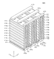
図17は本発明の不揮発性メモリ装置の例示的な形態を示す斜視図である。図17を参照すると、図2または図13のセルアレイ121、221は複数のメモリブロックBLKiを含むことができる。複数のメモリブロックBLKiはセルストリングが基板に対して垂直方向(z方向)に形成される3次元の積層構造によって形成される。
FIG. 17 is a perspective view showing an exemplary form of the nonvolatile memory device of the present invention. Referring to FIG. 17, the
基板411上にx方向に沿って複数のドーピング領域412a、412b、412c、412dが形成される。
A plurality of
第1及び第2ドーピング領域412a、412b間の基板411の領域上にy方向に沿って伸びる複数の絶縁物質418がz方向に沿って順に提供される。例えば、複数の絶縁物質418はz方向に沿って特定の距離だけ離隔して形成される。
A plurality of insulating
第1及び第2ドーピング領域412a、412b間の基板411上部にy方向に沿って連続して配置され、z方向に沿って絶縁物質418を貫通するピラー413が形成される。ピラー413は絶縁物質418を貫通して基板411と接続される。ここで、ピラー413は第2及び第3ドーピング領域412b、412c間の基板上部と、第3及び第4ドーピング領域412c、412d間の基板上部にも形成される。
A
ピラー413の内部層413bは絶縁材料で構成される。例えば、ピラー413の内部層413bはシリコン酸化物(Silicon oxide)などの絶縁材料を含む。第1及び第2ドーピング領域412a、412b間の領域には絶縁材料418、ピラー413及び基板411の露出された表面に沿って絶縁膜415が提供される。例示的に、z方向に沿って提供される最後の絶縁材料418のz方向側の露出面に提供される絶縁膜415は除去できる。
The inner layer 413b of the
第1及び第2ドーピング領域412a、412b間の領域には絶縁膜415の露出された表面上に第1導電物質414a〜414iが提供される。例えば、基板411に隣接する絶縁材料418と基板411との間にy方向に沿って伸びている第1導電物質414aが提供される。より詳細に説明すると、基板411に隣接する絶縁材料418の下面の絶縁膜415と基板411の間にx方向に伸びる第1導電物質414aが提供される。そして、第2及び第3ドーピング領域412b、412c間の領域には第1及び第2ドーピング領域412a、412b上の構造と同じ構造が提供される。第3及び第4ドーピング領域412c、412d間の領域には第1及び第2ドーピング領域412a、412b上の構造と同じ構造が形成される。
First
複数のピラー413上にドレイン416がそれぞれ提供される。ドレイン416は第2タイプでドープされたシリコン材料である。ドレイン416上にx方向に延びている第2導電物質417a〜417cが提供される。第2導電物質417a〜417cはy方向に沿って順に配置される。第2導電物質417a〜417cのそれぞれは対応する領域のドレイン416と接続される。例示的に、ドレイン416と、x方向に延びている第2導電物質417cはコンタクトプラグ(Contact plug)を介して接続される。
A
ここで、第1導電物質414a〜414iはそれぞれワード線または選択線SSL、GSLを形成する。第1導電物質414a〜414iからワード線に形成されている一部の導電物質414b〜414hは同じ層に属しているものが相互に接続されている。メモリブロックBLKiは第1導電物質414a〜414iの全体が選択される場合に選択される。一方、本発明のサブ−ブロックは第1導電物質414a〜414iの一部だけが選択されることにより選択可能である。また、本発明では、第1導電物質414a〜414iの層数は例示的なものに過ぎない。第1導電物質414a〜414iの層数は工程技術や制御技術によって多様に変更することができる。
Here, the first
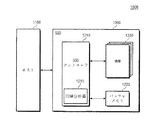
図18は本発明の実施形態によるソリッドステートディスク(以下、SSDと称する)を含むユーザ装置を示すブロック図である。図18を参照すると、ユーザ装置1000はホスト1100とSSD1200を備える。SSD1200はSSDコントローラ1210、バッファメモリ1220及び不揮発性メモリ装置1230を備える。
FIG. 18 is a block diagram showing a user apparatus including a solid state disk (hereinafter referred to as SSD) according to an embodiment of the present invention. Referring to FIG. 18, the
SSDコントローラ1210はホスト1100とSSD1200との物理的な接続を提供する。即ち、SSDコントローラ1210はホスト1100のバスフォーマット(Bus format)に対応してSSD1200とのインタフェースを提供する。特に、SSDコントローラ1210は回帰分析器1215を含むことができる。回帰分析器1215を介してメモリセルの分布谷の正確な位置を最小限の読み取り動作だけで検出することができる。したがって、読み取り失敗のとき、対応するメモリセルに対する最小限の読み取り動作で最適の読み取りレベルを検出することができる。
The
ホスト1100のバスフォーマット(Bus format)は、USB(Universal Serial Bus)、SCSI(Small Computer System Interface)、PCI express、ATA、PATA(Parallel ATA)、Serial ATA(SATA)、SAS(Serial Attached SCSI)などがある。
The bus format (Bus format) of the
バッファメモリ1220にはホスト1100から提供される書き込みデータまたは不揮発性メモリ装置1230から読み取られたデータが一時保存される。ホスト1100の読み取り要求時に不揮発性メモリ装置1230に存在するデータがキャッシュされている場合にはバッファメモリ1220は、キャッシュされたデータを直接ホスト1100に提供するキャッシュ機能を支援する。一般的に、ホスト1100のバスフォーマット(例えば、SATAまたはSAS)によるデータの伝送速度はSSD1200のメモリチャネルの伝送速度よりもっと速い。即ち、ホスト1100のインタフェース速度がもっと速い場合、大容量のバッファメモリ1220を提供することで速度差で発生するパフォーマンス低下を最小限に抑えることができる。
The
バッファメモリ1220は大容量の補助記憶装置として使用されるSSD1200から十分なバッファリングを提供するために同期式DRAM(Synchronous DRAM)で構成される。しかし、バッファメモリ1220はこれに限定されない。
The
不揮発性メモリ装置1230はSSD1200の記憶媒体として提供される。例えば、不揮発性メモリ装置1230は大容量の貯蔵能力を持つ垂直構造のNAND型フラッシュメモリ(NAND−type Flashmemory)で構成される。不揮発性メモリ装置1230は複数のメモリ装置で構成することができる。この場合、それぞれのメモリ装置はチャネル単位でSSDコントローラ1210と接続される。記憶媒体として不揮発性メモリ装置1230はNAND型フラッシュメモリを例に挙げて説明されたが、他の不揮発性メモリ装置で構成することができる。例えば、記憶媒体としてPRAM、MRAM、RERAM、FRAM(登録商標)、NOR型フラッシュメモリなどが使用でき、異種のメモリ装置が混在されているメモリシステムも適用することができる。不揮発性メモリ装置は実質的に図1に示したものと同様に構成することができる。
The
上述したSSD1200で、不揮発性メモリ装置1230は図2または図13の不揮発性メモリ装置と実質的に同様に動作することができる。即ち、不揮発性メモリ装置1230はSSDコントローラ1210のコマンドに基づいて検出されたデータ、検出されたデータの排他的論理和(XOR)、排他的論理和(XOR)の結果に含まれる論理‘1’の数のうち少なくとも1つを出力する。
With the above-described
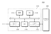
図19は本発明の他の実施形態によるメモリシステム2000を例示的に示すブロック図である。図19を参照すると、本発明によるメモリシステム2000はメモリコントローラ2100と不揮発性メモリ2200を備える。
FIG. 19 is a block diagram illustrating a
不揮発性メモリ2200は図2または図13の不揮発性メモリ装置と実質的に同様に構成することができる。従って、不揮発性メモリ2200に対する具体的な説明は省略する。
The
メモリコントローラ2100は不揮発性メモリ2200を制御するように構成される。SRAM2100はCPU2120のワーキングメモリとして使用される。ホストインタフェース2130はメモリシステム2000と接続されるホストのデータ交換プロトコルを備える。メモリコントローラ2100に備えられたECC2140は不揮発性メモリ2200から読み取られた読み取りデータに含まれているエラーを検出及び訂正する。メモリインタフェース2150は本発明の不揮発性メモリ2200とインタフェースする。CPU2120はメモリコントローラ2100のデータ交換のためのすべての制御動作を実行する。図面には図示されていないが、本発明によるメモリシステム2000はホスト(Host)とのインタフェースのためのコードデータを格納するROM(図示せず)などがさらに提供される。
The
メモリコントローラ2100はUSB、MMC、PCI−E、SAS、SATA、、PATA、SCSI、ESDI及びIDEなどの様々なインタフェースプロトコルのいずれかを介して外部(例えば、ホスト)と通信するように構成される。メモリコントローラ2100は選択されたメモリセルに対する読み取り電圧を回帰分析法を使用して決定する。回帰分析を実行する機能はファームウェアで提供されたり、特定の機能ブロックで提供されたりする。
The
本発明によるメモリシステム2000はコンピュータ、ラップトップ、UMPC(Ultra Mobile PC)、ワークステーション、ネットブック(net−book)、PDA、ポータブル(portable)コンピュータ、ウェブタブレット(web tablet)、コードレス電話(wireless phone)、携帯電話(mobile phone)、スマートフォン(smart phone)、デジタルカメラ(digital camera)、デジタルボイスレコーダ(digital audio recorder)、デジタル音声再生機(digital audio player)、デジタルビデオプレーヤー(digital picture player)、デジタルビデオレコーダ(digital video recorder)、デジタルビデオプレーヤー(digital video player)、情報を無線環境で送受信することができる装置、ホームネットワークを構成する様々なユーザ装置のいずれかを適用する。
The
図20は本発明の他の実施形態によるデータ保存装置3000を例示的に示すブロック図である。図20を参照すると、本発明によるデータ保存装置3000はフラッシュメモリ3100とメモリコントローラ3200を備える。メモリコントローラ3200はデータ保存装置3000の外部から受信された制御信号に基づいてフラッシュメモリ3100を制御する。
FIG. 20 is a block diagram illustrating a
上述したデータ保存装置3000で、フラッシュメモリ3100は図2または図13の不揮発性メモリ装置と実質的に同様に動作する。即ち、フラッシュメモリ3100は選択されたメモリセルに対して互いに異なる読み取り電圧として読み出してメモリコントローラ3200に提供する。フラッシュメモリ3100は読み出されたデータを排他的論理和演算を実行した後にメモリコントローラ3200に提供する。フラッシュメモリ3100は読み出されたデータ間の排他的論理和演算の結果に含まれる論理‘1’の数をメモリコントローラ3200に提供する。
In the
メモリコントローラ3200はフラッシュメモリ3100からのデータを参照して選択されたメモリセルの最適な読み込みレベルを決定するための回帰分析を行う。回帰分析を通じて最小の読み取り回数だけで信頼性の高い読み取りレベルを決定することができる。
The
本発明のデータ保存装置3000はメモリカード装置、SSD装置、マルチメディアカード装置、SDカード、メモリスティック装置、ハードディスクドライブ装置、ハイブリッドドライブまたはユニバーサルシリアルバスフラッシュデバイスを構成する。例えば、本発明のデータ保存装置3000はデジタル、カメラ、パソコンなどのユーザ装置を使用するための業界標準を満たしているカードを構成する。
The
図21は本発明によるフラッシュメモリ装置4100及びそれを含むコンピューティング・システム4000の概略的な構成を示す図である。図21を参照すると、本発明によるコンピューティングシステム4000はバス4600に電気的に接続された不揮発性メモリ装置4120、メモリコントローラ4110、マイクロプロセッサ4200、RAM4300、ユーザインタフェース4400、ベースバンドチップセット(baseband chipset)のようなモデム4500などを含む。図21に図示されたメモリコントローラ4110と不揮発性メモリ装置4120はメモリシステム4100を構成する。メモリシステム4100は図1、図12、図15、図18、図19、図20に示されたメモリシステムのいずれかである。
FIG. 21 is a diagram showing a schematic configuration of a
本発明によるコンピューティングシステムがモバイルデバイスである場合は、コンピューティングシステムの動作電圧を供給するためのバッテリーがさらに提供される。図面には図示されていないが、本発明によるコンピューティングシステムはアプリケーションチップセット(application chipset)、カメライメージプロセッサ(Camera Image Processor:CIS)、モバイルDRAMなどがさらに提供される。メモリシステム4100は前述した本発明の回帰分析法を通じて最適の読み取りレベルを決定する。そのため、データの信頼性(Data Integrity)を向上させることができる。
When the computing system according to the present invention is a mobile device, a battery for supplying the operating voltage of the computing system is further provided. Although not shown in the drawings, the computing system according to the present invention further includes an application chipset, a camera image processor (CIS), a mobile DRAM, and the like. The
本発明による半導体装置は様々な形態のパッケージを利用して実装することができる。例えば、本発明による半導体及び/またはコントローラはPoP(Package on Package)、BGAs(Ball grid arrays)、CSPs(Chip scale packages)、PLCC(Plastic Leaded Chip Carrier)、PDIP(Plastic Dual In−Line Package)、Die in Waffle Pack、Die in Wafer Form、COB(Chip On Board)、CERDIP(Ceramic Dual In−Line Package)、MQFP(Plastic Metric Quad Flat Pack)、TQFP(Thin Quad Flat Pack)、SOIC(Small Out lineIntegrated Circuit)、SSOP(Shrink Small Outline Package)、TSOP(Thin Small Outline)、TQFP(Thin Quad Flatpack)、SIP(SystemIn Package)、MCP(Multi Chip Package)、WFP(Wafer−level Fabricated Package)、WSP(Wafer−Level Processed Stack Package)などのパッケージを使用して実装される。 The semiconductor device according to the present invention can be mounted using various types of packages. For example, the semiconductor and / or the controller according to the present invention may be PoP (Package on Package), BGAs (Ball grid arrays), CSPs (Chip scale package carriers), PLCC (Plastic Leaded Chip Carrier), PDIP (Plastic-Duy-Led-Dip, Die in Waffle Pack, Die in Wafer Form, COB (Chip On Board), CERDIP (Ceramic Dual In-Line Package), MQFP (Plastic Metric Quad Pt, Tac Pack) tegrated Circuit), SSOP (Shrink Small Outline Package), TSOP (Thin Small Flatline), TQFP (Thin Quad Flatpack), SIP (SystemInWard), MCP (MultiPh), MCP (MultiPh) It is implemented using a package such as Wafer-Level Processed Stack Package.
以上のように、図面と明細書に最良の実施形態が開示された。ここで特定の用語が使用されたが、これは単に本発明を説明するための目的で使用されたので意味限定や特許請求の範囲に記載された本発明の範囲を制限しない。そのため、本発明の技術分野の通常の知識を有する者であれば、多様な変形及び均等な他の実施形態が可能であることを理解できるだろう。したがって、本発明の真の技術的保護範囲は特許請求の範囲の技術的思想により定められなければならない。 As described above, the best embodiment has been disclosed in the drawings and specification. Although specific terminology has been used herein, it is used merely for the purpose of describing the present invention and does not limit the meaning or scope of the invention as set forth in the claims. Therefore, those skilled in the art of the present invention can understand that various modifications and other equivalent embodiments are possible. Therefore, the true technical protection scope of the present invention must be determined by the technical idea of the claims.
110、210、310 メモリコントローラ
112、227、327 ビットカウンタ
114、214、314 回帰分析器
120、220、320 不揮発性メモリ装置
121、221 セルアレイ
122、222 行デコーダ
123、223 ページバッファ
124、224 入出力バッファ
125、225 制御ロジック
126、226 電圧発生器
130、140、150、160、170 分布谷
411 基板
412a、412b、412c、412d ドーピング領域
413 ピラー
413a 表面層
413b 内部の層
414a〜414i 第1導電物質
415 絶縁膜
416 ドレイン
417a、417b、417c ビット線
418 絶縁材料
1100 ホスト
1200 SSD
1210 SSDコントローラ
1215 回帰分析器
1220 バッファメモリ
1230 不揮発性メモリ装置
2100 メモリコントローラ
2110 SRAM
2120 CPU
2130 ホストインタフェース
2140 ECC
2150 メモリインタフェース
2200 不揮発性メモリ装置
3100 フラッシュメモリ
3200 フラッシュコントローラ
4000 コンピューティングシステム
4100 メモリシステム
4110 メモリコントローラ
4120 フラッシュメモリ装置
4200 マイクロプロセッサ
4300 RAM
4400 ユーザインタフェース
4500 モデム
4600 システムバス
110, 210, 310
1210
2120 CPU
2130
2150
4400
Claims (19)
互いに異なる読み取り電圧に選択されたメモリセルを読み出す段階と、
前記互いに異なる読み取り電圧によって読み出されたデータを参照して複数のしきい値電圧帯域に各々対応するメモリセルの数をカウントする段階と、
前記複数のしきい値電圧帯域に各々含まれるメモリセルの数を参照して前記選択されたメモリセルのしきい値電圧に対する確率密度関数の座標値を決定する段階と、
前記座標値を参照して前記確率密度関数の係数を求める段階と、
前記確率密度関数の傾きが0である座標点のしきい値電圧を前記選択されたメモリセルの読み取り電圧に決定する段階を含むことを特徴とする読み取り方法。 In a reading method of a nonvolatile memory device,
Reading selected memory cells to different read voltages;
Counting the number of memory cells each corresponding to a plurality of threshold voltage bands with reference to the data read by the different read voltages;
Determining a coordinate value of a probability density function for a threshold voltage of the selected memory cell with reference to the number of memory cells included in each of the plurality of threshold voltage bands;
Obtaining a coefficient of the probability density function with reference to the coordinate values;
A reading method comprising: determining a threshold voltage of a coordinate point having a slope of the probability density function of 0 as a reading voltage of the selected memory cell.
第1読み取り電圧によって読み出された第1データ及び第2読み取り電圧によって読み出された第2データの同じ列に対応するデータビットに排他的論理和演算を実行する段階と、
前記排他的論理和演算の結果から論理‘1’の数をカウントする段階を含むことを特徴とする請求項1に記載の読み取り方法。 The step of counting the number of memory cells includes:
Performing an exclusive OR operation on data bits corresponding to the same column of first data read by a first read voltage and second data read by a second read voltage;
The reading method according to claim 1, further comprising a step of counting the number of logic '1's from the result of the exclusive OR operation.
前記確率密度関数を微分する段階と、
微分された前記確率密度関数の値を0とする方程式の根を求める段階を含むことを特徴とする請求項1に記載の読み取り方法。 Determining the read voltage comprises:
Differentiating the probability density function;
The reading method according to claim 1, further comprising: obtaining a root of an equation in which the value of the differentiated probability density function is zero.
前記読み出されたデータを参照して前記メモリセルのしきい値電圧に対する確率分布関数を求め、前記確率分布関数の導関数を解析して前記メモリセルの読み取り電圧を決定するメモリコントローラを含み、
前記不揮発性メモリ装置は、第1読み取りレベルに応じて読み出された第1データと、第2読み取りレベルによって読み出された第2データに対する排他的論理和演算を実行し、前記排他的論理和演算の結果に含まれる論理‘1’の数をカウントして前記確率分布関数の座標値として提供されるビットカウンタを含むことを特徴とするメモリシステム。 A non-volatile memory device that reads data from the selected memory cell in response to a read command including read level information;
Determine the probability distribution function for the threshold voltage of the memory cell with reference to the read data, see contains a memory controller for determining a read voltage of the memory cell by analyzing the derivative of the probability distribution function ,
The non-volatile memory device performs an exclusive OR operation on the first data read according to the first read level and the second data read at the second read level, and the exclusive OR A memory system comprising: a bit counter provided as a coordinate value of the probability distribution function by counting the number of logic '1' included in an operation result .
り回数に関する情報が含まれていることを特徴とする請求項11に記載のメモリシステム。 12. The memory system according to claim 11, wherein the read level information includes information on an initial read level, a voltage interval size, and a read count.
Applications Claiming Priority (2)
| Application Number | Priority Date | Filing Date | Title |
|---|---|---|---|
| KR10-2012-0119106 | 2012-10-25 | ||
| KR1020120119106A KR102038408B1 (en) | 2012-10-25 | 2012-10-25 | Semiconductor memory system using regression alalysis and read method thereof |
Publications (3)
| Publication Number | Publication Date |
|---|---|
| JP2014086128A JP2014086128A (en) | 2014-05-12 |
| JP2014086128A5 JP2014086128A5 (en) | 2016-12-08 |
| JP6345407B2 true JP6345407B2 (en) | 2018-06-20 |
Family
ID=50547061
Family Applications (1)
| Application Number | Title | Priority Date | Filing Date |
|---|---|---|---|
| JP2013220910A Active JP6345407B2 (en) | 2012-10-25 | 2013-10-24 | Memory system using regression analysis method and reading method thereof |
Country Status (4)
| Country | Link |
|---|---|
| US (2) | US9111626B2 (en) |
| JP (1) | JP6345407B2 (en) |
| KR (1) | KR102038408B1 (en) |
| CN (2) | CN110085275B (en) |
Families Citing this family (57)
| Publication number | Priority date | Publication date | Assignee | Title |
|---|---|---|---|---|
| KR102038408B1 (en) * | 2012-10-25 | 2019-10-30 | 삼성전자주식회사 | Semiconductor memory system using regression alalysis and read method thereof |
| KR101503822B1 (en) * | 2013-10-14 | 2015-03-18 | 주식회사 디에이아이오 | Non-volatile memory device |
| KR102174030B1 (en) * | 2014-05-13 | 2020-11-05 | 삼성전자주식회사 | Storage device including nonvolatile memory device and read method thereof |
| KR20160005264A (en) * | 2014-07-04 | 2016-01-14 | 삼성전자주식회사 | Storage device and read methods thereof |
| US9741431B2 (en) * | 2014-11-10 | 2017-08-22 | Sk Hynix Memory Solutions Inc. | Optimal read threshold estimation |
| US9720754B2 (en) | 2014-11-20 | 2017-08-01 | Western Digital Technologies, Inc. | Read level grouping for increased flash performance |
| US9576671B2 (en) | 2014-11-20 | 2017-02-21 | Western Digital Technologies, Inc. | Calibrating optimal read levels |
| US9905302B2 (en) | 2014-11-20 | 2018-02-27 | Western Digital Technologies, Inc. | Read level grouping algorithms for increased flash performance |
| KR102397016B1 (en) * | 2014-11-24 | 2022-05-13 | 삼성전자주식회사 | Operatiing method of nonvolatile memory system |
| KR102396422B1 (en) * | 2015-02-11 | 2022-05-11 | 삼성전자주식회사 | Nonvolatile memory and storage device including nonvolatile memory |
| US9785383B2 (en) | 2015-03-09 | 2017-10-10 | Toshiba Memory Corporation | Memory system and method of controlling nonvolatile memory |
| US10180876B2 (en) * | 2015-08-04 | 2019-01-15 | Toshiba Memory Corporation | Memory controller and semiconductor memory device |
| KR102459077B1 (en) | 2016-01-12 | 2022-10-27 | 삼성전자주식회사 | Memory system using non-linear filtering shceme and read method thereof |
| KR102585221B1 (en) | 2016-04-21 | 2023-10-05 | 삼성전자주식회사 | Memory Device, Memory System and Method of Operating Memory Device |
| KR102589259B1 (en) | 2016-06-20 | 2023-10-12 | 에스케이하이닉스 주식회사 | Data storage device and operating method thereof |
| US9679661B1 (en) | 2016-06-28 | 2017-06-13 | Sandisk Technologies Llc | Non-volatile storage system with self-test for read performance enhancement feature setup |
| US9672940B1 (en) | 2016-08-18 | 2017-06-06 | Sandisk Technologies Llc | Non-volatile memory with fast read process |
| JP6674361B2 (en) * | 2016-09-29 | 2020-04-01 | キオクシア株式会社 | Memory system |
| KR102643916B1 (en) | 2016-10-18 | 2024-03-08 | 삼성전자주식회사 | Storage device, memory system, and read voltage decision method thererof |
| KR102302187B1 (en) | 2017-03-13 | 2021-09-14 | 삼성전자주식회사 | Methods of operating nonvolatile memory devices and nonvolatile memory devices |
| US10140040B1 (en) | 2017-05-25 | 2018-11-27 | Micron Technology, Inc. | Memory device with dynamic program-verify voltage calibration |
| KR102353405B1 (en) | 2017-09-19 | 2022-01-19 | 삼성전자주식회사 | Pre-processing system, apparatus and method of characteristic data and memory control system using the same |
| US10366763B2 (en) * | 2017-10-31 | 2019-07-30 | Micron Technology, Inc. | Block read count voltage adjustment |
| KR102427638B1 (en) | 2018-01-10 | 2022-08-01 | 삼성전자주식회사 | Non-volatile memory device and read method thereof |
| KR102506507B1 (en) * | 2018-01-19 | 2023-03-07 | 삼성전자주식회사 | Apparatus and method for transmitting and receiving signal in multimedia system |
| CN110120234B (en) * | 2018-02-07 | 2022-04-15 | 北京忆芯科技有限公司 | Solid-state memory device and method for searching for optimum read threshold voltage thereof |
| KR102617350B1 (en) | 2018-03-14 | 2023-12-26 | 삼성전자주식회사 | Memory controller, operating method thereof and storage device including the same |
| CN110400593B (en) * | 2018-04-24 | 2021-08-03 | 群联电子股份有限公司 | Memory management method, memory storage device and memory control circuit unit |
| US10664194B2 (en) | 2018-05-16 | 2020-05-26 | Micron Technology, Inc. | Memory system with dynamic calibration using a variable adjustment mechanism |
| US10566063B2 (en) | 2018-05-16 | 2020-02-18 | Micron Technology, Inc. | Memory system with dynamic calibration using a trim management mechanism |
| US10990466B2 (en) | 2018-06-20 | 2021-04-27 | Micron Technology, Inc. | Memory sub-system with dynamic calibration using component-based function(s) |
| CN110797069B (en) * | 2018-08-01 | 2021-10-22 | 群联电子股份有限公司 | Voltage adjusting method, memory control circuit unit and memory storage device |
| JP2020047339A (en) | 2018-09-18 | 2020-03-26 | キオクシア株式会社 | Memory system |
| KR102535110B1 (en) | 2018-10-01 | 2023-05-23 | 에스케이하이닉스 주식회사 | Storage device and operating method thereof |
| KR102599123B1 (en) | 2018-11-14 | 2023-11-06 | 삼성전자주식회사 | Storage device inferring read levels based on artificial neural network model and learning method of artificial neural network model |
| US11158369B2 (en) * | 2018-12-26 | 2021-10-26 | Western Digital Technologies, Inc. | On-chip non-volatile memory (NVM) search |
| US11163483B2 (en) | 2018-12-31 | 2021-11-02 | SK Hynix Inc. | Robust detection techniques for updating read voltages of memory devices |
| US11256778B2 (en) * | 2019-02-14 | 2022-02-22 | Micron Technology, Inc. | Methods and apparatus for checking the results of characterized memory searches |
| US11327551B2 (en) | 2019-02-14 | 2022-05-10 | Micron Technology, Inc. | Methods and apparatus for characterizing memory devices |
| TWI690929B (en) * | 2019-04-11 | 2020-04-11 | 點序科技股份有限公司 | Memory apparatus and method for adjusting reading reference voltage thereof |
| KR20210024912A (en) * | 2019-08-26 | 2021-03-08 | 에스케이하이닉스 주식회사 | Storage device and operating method thereof |
| KR20210083466A (en) | 2019-12-26 | 2021-07-07 | 삼성전자주식회사 | Storage device and operating method of storage device |
| JP7087013B2 (en) * | 2020-03-06 | 2022-06-20 | キオクシア株式会社 | Memory system and non-volatile memory control method |
| US11265021B2 (en) * | 2020-03-10 | 2022-03-01 | SK Hynix Inc. | Apparatus and method for error recovery in memory system |
| US11024401B1 (en) | 2020-05-07 | 2021-06-01 | Micron Technology, Inc. | Compute an optimized read voltage |
| US11238953B2 (en) | 2020-05-07 | 2022-02-01 | Micron Technology, Inc. | Determine bit error count based on signal and noise characteristics centered at an optimized read voltage |
| US11049582B1 (en) | 2020-05-07 | 2021-06-29 | Micron Technology, Inc. | Detection of an incorrectly located read voltage |
| US11177013B1 (en) * | 2020-05-07 | 2021-11-16 | Micron Technology, Inc. | Determine signal and noise characteristics centered at an optimized read voltage |
| KR20220029233A (en) | 2020-09-01 | 2022-03-08 | 삼성전자주식회사 | Page buffer circuit and memory device including the same |
| KR20220139685A (en) | 2021-04-08 | 2022-10-17 | 에스케이하이닉스 주식회사 | Semiconductor memory device and operating method thereof |
| KR102558145B1 (en) * | 2021-05-20 | 2023-07-25 | 한국전자통신연구원 | Method for generating gaussian error data using flash memory and apparatus using the same |
| KR102460717B1 (en) * | 2021-08-17 | 2022-10-31 | 삼성전자주식회사 | Memory Controller calculating optimal read level, Memory System having the same and Operating Method of Memory Controller |
| KR102491652B1 (en) | 2021-09-17 | 2023-01-27 | 삼성전자주식회사 | Storage controller determining a distribution type, method of operating the same, and method of operating storage device having the same |
| EP4152332A1 (en) * | 2021-09-17 | 2023-03-22 | Samsung Electronics Co., Ltd. | Storage controller determining distribution type, method of operating the same, and method of operating storage device including the same |
| KR102491655B1 (en) | 2021-10-01 | 2023-01-27 | 삼성전자주식회사 | Storage controller determining an error count, method of operating the same, and method of operating storage device having the same |
| EP4160603A1 (en) * | 2021-10-01 | 2023-04-05 | Samsung Electronics Co., Ltd. | Storage controller determining error count, method of operating the same, and method of operating storage device including the same |
| US11853590B2 (en) * | 2021-12-02 | 2023-12-26 | SK Hynix Inc. | Read threshold estimation system using calculations based on polynomial regression |
Family Cites Families (31)
| Publication number | Priority date | Publication date | Assignee | Title |
|---|---|---|---|---|
| DE19845441C2 (en) | 1998-10-02 | 2003-01-16 | Ficht Gmbh & Co Kg | Method for electronically trimming an injector |
| JP2003298877A (en) * | 2002-03-29 | 2003-10-17 | Fujitsu General Ltd | Nonlinear processing circuit |
| JP4660243B2 (en) * | 2005-03-28 | 2011-03-30 | 株式会社東芝 | Semiconductor memory device |
| US7649793B1 (en) * | 2006-05-04 | 2010-01-19 | Marvell International Ltd. | Channel estimation for multi-level memories using pilot signals |
| US8725929B1 (en) * | 2006-11-06 | 2014-05-13 | Marvell World Trade Ltd. | Adaptive read and write systems and methods for memory cells |
| US7941590B2 (en) * | 2006-11-06 | 2011-05-10 | Marvell World Trade Ltd. | Adaptive read and write systems and methods for memory cells |
| CN101715595A (en) | 2007-03-12 | 2010-05-26 | 爱诺彼得技术有限责任公司 | Adaptive estimation of memory cell read thresholds |
| JP2008251138A (en) | 2007-03-30 | 2008-10-16 | Toshiba Corp | Nonvolatile semiconductor memory, control method of nonvolatile semiconductor memory, nonvolatile semiconductor memory system, and memory card |
| KR100888842B1 (en) | 2007-06-28 | 2009-03-17 | 삼성전자주식회사 | Flash memory device optimizing read voltage and method for optimizing read voltage thereof |
| KR20090048108A (en) | 2007-11-09 | 2009-05-13 | 주식회사 하이닉스반도체 | Non volatile memory device and reading out method therof |
| KR100953047B1 (en) * | 2007-12-28 | 2010-04-14 | 주식회사 하이닉스반도체 | Method of operating a non volatile memory device |
| KR20090117172A (en) | 2008-05-08 | 2009-11-12 | 삼성전자주식회사 | Memory device and memory data read method |
| KR101391362B1 (en) | 2008-07-23 | 2014-05-07 | 삼성전자주식회사 | Flash memory system configuring reading voltage level and configuration method of reading voltage level |
| KR101516577B1 (en) | 2008-11-10 | 2015-05-06 | 삼성전자주식회사 | Nonvolatile semi-conductor memory device and method for calculating read voltage non-volatile semiconductor memory device |
| US8120953B2 (en) | 2008-12-11 | 2012-02-21 | Samsung Electronics Co., Ltd. | Reading method of nonvolatile semiconductor memory device |
| US8184480B2 (en) | 2008-12-11 | 2012-05-22 | Samsung Electronics Co., Ltd. | Multi-level nonvolatile memory device with reduced number of read voltages based on a cell address and method for operating the same |
| KR101578511B1 (en) * | 2009-05-20 | 2015-12-18 | 삼성전자주식회사 | Method for setting a read voltage |
| KR101586046B1 (en) * | 2009-05-26 | 2016-01-18 | 삼성전자주식회사 | Storage device and reading method thereof |
| JP5361603B2 (en) * | 2009-08-13 | 2013-12-04 | 株式会社東芝 | controller |
| US8072805B2 (en) * | 2009-08-18 | 2011-12-06 | Skymedi Corporation | Method and system of finding a read voltage for a flash memory |
| KR101618311B1 (en) * | 2010-02-08 | 2016-05-04 | 삼성전자주식회사 | Flash memory device and reading method thereof |
| KR20110128436A (en) | 2010-05-24 | 2011-11-30 | 삼성전자주식회사 | Method for tracking read level for non-volatile memory, memory controller performing the same and recording medium |
| US20120008414A1 (en) | 2010-07-06 | 2012-01-12 | Michael Katz | Systems and methods for storing, retrieving, and adjusting read thresholds in flash memory storage system |
| US8508995B2 (en) | 2010-09-15 | 2013-08-13 | Densbits Technologies Ltd. | System and method for adjusting read voltage thresholds in memories |
| JP2012133832A (en) | 2010-12-20 | 2012-07-12 | Samsung Yokohama Research Institute Co Ltd | Nonvolatile semiconductor memory device and read-out voltage detection method |
| KR101919902B1 (en) * | 2011-10-18 | 2018-11-20 | 삼성전자 주식회사 | Method of reading data in memory device |
| KR101858560B1 (en) * | 2011-11-24 | 2018-05-18 | 삼성전자주식회사 | Method for operating non-volatile memory device and method for operating memory system having the same |
| KR20140013401A (en) * | 2012-07-23 | 2014-02-05 | 삼성전자주식회사 | Memory device, memory system and method of controlling a read voltage of the memory device |
| KR101939234B1 (en) * | 2012-07-23 | 2019-01-16 | 삼성전자 주식회사 | Memory device, memory system and method of controlling a read voltage of the memory device |
| KR102038408B1 (en) * | 2012-10-25 | 2019-10-30 | 삼성전자주식회사 | Semiconductor memory system using regression alalysis and read method thereof |
| US9147490B2 (en) * | 2013-03-15 | 2015-09-29 | Sandisk Technologies Inc. | System and method of determining reading voltages of a data storage device |
-
2012
- 2012-10-25 KR KR1020120119106A patent/KR102038408B1/en active IP Right Grant
-
2013
- 2013-10-24 JP JP2013220910A patent/JP6345407B2/en active Active
- 2013-10-24 US US14/062,092 patent/US9111626B2/en active Active
- 2013-10-25 CN CN201910211592.4A patent/CN110085275B/en active Active
- 2013-10-25 CN CN201310511873.4A patent/CN103778962B/en active Active
-
2015
- 2015-07-28 US US14/811,222 patent/US9552887B2/en active Active
Also Published As
| Publication number | Publication date |
|---|---|
| CN103778962A (en) | 2014-05-07 |
| KR102038408B1 (en) | 2019-10-30 |
| KR20140052691A (en) | 2014-05-07 |
| CN110085275B (en) | 2023-07-25 |
| US20150332778A1 (en) | 2015-11-19 |
| JP2014086128A (en) | 2014-05-12 |
| US20140119124A1 (en) | 2014-05-01 |
| US9552887B2 (en) | 2017-01-24 |
| CN103778962B (en) | 2019-04-16 |
| US9111626B2 (en) | 2015-08-18 |
| CN110085275A (en) | 2019-08-02 |
Similar Documents
| Publication | Publication Date | Title |
|---|---|---|
| JP6345407B2 (en) | Memory system using regression analysis method and reading method thereof | |
| KR102302187B1 (en) | Methods of operating nonvolatile memory devices and nonvolatile memory devices | |
| US8804422B2 (en) | Nonvolatile memory device and related method of operation | |
| US8839080B2 (en) | Methods of performing error detection/correction in nonvolatile memory devices | |
| US9324420B2 (en) | Method of estimating deterioration state of memory device and related method of wear leveling | |
| KR101944793B1 (en) | Flash memory system including flash memory and detecting method of abnormal wordline thereof | |
| KR102585221B1 (en) | Memory Device, Memory System and Method of Operating Memory Device | |
| US8503230B2 (en) | Access method of non-volatile memory device | |
| KR101934892B1 (en) | Method for determining deterioration state of memory device and memory system using method thereof | |
| KR101518033B1 (en) | Multi-level non-volatile semiconductor device, memory system having the same and Operating method there-of | |
| KR20170097267A (en) | Data storage device including read voltage search unit | |
| KR20140113190A (en) | Method of optimizing llr used in nonvolatile memory device and method of correcting error in nonvolatile memory device | |
| US8631306B2 (en) | Method and memory system using a priori probability information to read stored data | |
| US20210366562A1 (en) | Memory system processing request based on inference and operating method of the same | |
| US10535406B2 (en) | Storage device and copy-back method thereof | |
| US9965005B2 (en) | Memory diagnosis system | |
| CN113223593A (en) | Method for optimizing reading voltage of memory cell, controller of 3D memory and operation method thereof | |
| US11887680B2 (en) | Reducing program verifies for multi-level NAND cells | |
| US20240069790A1 (en) | Memory controller, a storage device, and an operating method of the storage device | |
| CN116246683A (en) | Reading threshold prediction in a memory device using a deep neural network | |
| KR20240048306A (en) | Generalized ldpc encoder, generalized ldpc encoding method and storage device |
Legal Events
| Date | Code | Title | Description |
|---|---|---|---|
| RD04 | Notification of resignation of power of attorney |
Free format text: JAPANESE INTERMEDIATE CODE: A7424 Effective date: 20141226 |
|
| A521 | Request for written amendment filed |
Free format text: JAPANESE INTERMEDIATE CODE: A523 Effective date: 20161021 |
|
| A621 | Written request for application examination |
Free format text: JAPANESE INTERMEDIATE CODE: A621 Effective date: 20161021 |
|
| A977 | Report on retrieval |
Free format text: JAPANESE INTERMEDIATE CODE: A971007 Effective date: 20171013 |
|
| A131 | Notification of reasons for refusal |
Free format text: JAPANESE INTERMEDIATE CODE: A131 Effective date: 20171023 |
|
| A521 | Request for written amendment filed |
Free format text: JAPANESE INTERMEDIATE CODE: A523 Effective date: 20180115 |
|
| TRDD | Decision of grant or rejection written | ||
| A01 | Written decision to grant a patent or to grant a registration (utility model) |
Free format text: JAPANESE INTERMEDIATE CODE: A01 Effective date: 20180423 |
|
| A61 | First payment of annual fees (during grant procedure) |
Free format text: JAPANESE INTERMEDIATE CODE: A61 Effective date: 20180523 |
|
| R150 | Certificate of patent or registration of utility model |
Ref document number: 6345407 Country of ref document: JP Free format text: JAPANESE INTERMEDIATE CODE: R150 |
|
| R250 | Receipt of annual fees |
Free format text: JAPANESE INTERMEDIATE CODE: R250 |
|
| R250 | Receipt of annual fees |
Free format text: JAPANESE INTERMEDIATE CODE: R250 |
|
| R250 | Receipt of annual fees |
Free format text: JAPANESE INTERMEDIATE CODE: R250 |