JP6327770B2 - Battery pack - Google Patents
Battery pack Download PDFInfo
- Publication number
- JP6327770B2 JP6327770B2 JP2017126380A JP2017126380A JP6327770B2 JP 6327770 B2 JP6327770 B2 JP 6327770B2 JP 2017126380 A JP2017126380 A JP 2017126380A JP 2017126380 A JP2017126380 A JP 2017126380A JP 6327770 B2 JP6327770 B2 JP 6327770B2
- Authority
- JP
- Japan
- Prior art keywords
- power
- battery
- battery pack
- board
- wiring
- Prior art date
- Legal status (The legal status is an assumption and is not a legal conclusion. Google has not performed a legal analysis and makes no representation as to the accuracy of the status listed.)
- Active
Links
Images
Classifications
-
- Y—GENERAL TAGGING OF NEW TECHNOLOGICAL DEVELOPMENTS; GENERAL TAGGING OF CROSS-SECTIONAL TECHNOLOGIES SPANNING OVER SEVERAL SECTIONS OF THE IPC; TECHNICAL SUBJECTS COVERED BY FORMER USPC CROSS-REFERENCE ART COLLECTIONS [XRACs] AND DIGESTS
- Y02—TECHNOLOGIES OR APPLICATIONS FOR MITIGATION OR ADAPTATION AGAINST CLIMATE CHANGE
- Y02E—REDUCTION OF GREENHOUSE GAS [GHG] EMISSIONS, RELATED TO ENERGY GENERATION, TRANSMISSION OR DISTRIBUTION
- Y02E60/00—Enabling technologies; Technologies with a potential or indirect contribution to GHG emissions mitigation
- Y02E60/10—Energy storage using batteries
Landscapes
- Battery Mounting, Suspending (AREA)
- Connection Of Batteries Or Terminals (AREA)
Description
本発明は、複数の薄板状の電池セルが積み重ねられた電気積層体を備えた電池パックに関する。 The present invention relates to a battery pack including an electrical laminate in which a plurality of thin plate-like battery cells are stacked.
リチウムイオン二次電池に代表される非水電解質電池は、エネルギー密度が高いという特徴から、自動車やバイク等の各種移動機器、携帯情報端末、無停電電源装置(UPS(Uninterruptible Power Supply))、蓄電装置等の電源として利用されている。このような用途において、エネルギー密度を更に向上させるため、可撓性を有するラミネートシートで発電要素を外装した薄板状のラミネート形リチウムイオン二次電池が多く使用されている。更に、所望する電池容量を得るために、複数の薄板状の二次電池(電池セル)を積み重ねてこれらを直列に接続した電池積層体も実用されている(例えば特許文献1参照)。 Non-aqueous electrolyte batteries typified by lithium-ion secondary batteries are characterized by high energy density. Therefore, various mobile devices such as cars and motorcycles, personal digital assistants, uninterruptible power supplies (UPSs), and electricity storage It is used as a power source for devices. In such applications, in order to further improve the energy density, a thin plate-like laminated lithium ion secondary battery in which a power generation element is packaged with a flexible laminate sheet is often used. Furthermore, in order to obtain a desired battery capacity, a battery stack in which a plurality of thin plate-like secondary batteries (battery cells) are stacked and these are connected in series is also in practical use (see, for example, Patent Document 1).
複数の電池セルを積層した電池積層体は回路基板とともに筐体内に収納されて電池パックとなる。回路基板には、電池積層体と外部接続端子とをつなぐパワー配線と保護回路とが設けられている。保護回路は、パワー配線の電流を監視する電流監視部、電池積層体を構成する各電池セルの電圧を監視する電圧監視部、上記電流監視部及び上記電圧監視部からの出力により異常を検知するとパワー配線を遮断する信号を出力する制御部を備えている。従来の電池パックでは、パワー配線と保護回路を構成する各種機能部品とが、共通する1枚の基板上に設けられる(特許文献2参照)。 A battery stack in which a plurality of battery cells are stacked is housed in a housing together with a circuit board to form a battery pack. The circuit board is provided with a power wiring and a protection circuit for connecting the battery stack and the external connection terminal. When the protection circuit detects an abnormality by an output from the current monitoring unit that monitors the current of the power wiring, the voltage monitoring unit that monitors the voltage of each battery cell constituting the battery stack, the current monitoring unit, and the voltage monitoring unit. A control unit that outputs a signal for shutting off the power wiring is provided. In a conventional battery pack, power wiring and various functional parts constituting a protection circuit are provided on a common substrate (see Patent Document 2).
電池パックに対して小型化且つ大容量化の要望が日増しに高まっている。この要望に応えるためには、基板を小型化する一方で、パワー配線に流れる電流を増大させる必要がある。 The demand for smaller and larger capacity battery packs is increasing day by day. In order to meet this demand, it is necessary to increase the current flowing through the power wiring while reducing the size of the substrate.
ところが、パワー配線の電流を増大させるために、基板上に形成されたパワー配線の幅を増大させると、基板を小型化することが困難になる。また、パワー配線の電流を増大させると、パワー配線から発生するノイズが、電圧監視部や制御部を構成するデジタル回路に及ぼす悪影響を無視できなくなる。 However, if the width of the power wiring formed on the substrate is increased in order to increase the current of the power wiring, it becomes difficult to reduce the size of the substrate. Further, if the current of the power wiring is increased, the adverse effect of noise generated from the power wiring on the digital circuits constituting the voltage monitoring unit and the control unit cannot be ignored.
本発明は、従来の電池パックの上記の課題を解決し、小型化且つ大容量化が実現された電池パックを提供することを目的とする。 An object of the present invention is to solve the above-described problems of conventional battery packs and to provide a battery pack that is reduced in size and increased in capacity.
本発明の電池パックは、複数の薄板状の電池セルが積み重ねられ且つ前記複数の電池セルが直列に接続された電池積層体と、前記複数の電池セルのそれぞれの電圧を監視する電圧監視部と、前記電池積層体と外部接続端子とをつなぐパワー配線、前記パワー配線の電流を監視する電流監視部、及び、前記パワー配線を断続するスイッチを有するパワー部と、前記電圧監視部及び前記電流監視部からの信号が入力され、前記パワー配線を遮断する信号を前記スイッチに出力する制御部とを備える。前記パワー部は、前記電圧監視部及び前記制御部が設けられた基板とは別のパワー基板に設けられている。前記パワー基板に形成された配線は、前記電圧監視部及び前記制御部が設けられた基板に形成された配線より厚い。 The battery pack of the present invention includes a battery stack in which a plurality of thin plate-like battery cells are stacked and the plurality of battery cells are connected in series, and a voltage monitoring unit that monitors each voltage of the plurality of battery cells; A power wiring that connects the battery stack and the external connection terminal, a current monitoring unit that monitors a current of the power wiring, a power unit that includes a switch that interrupts the power wiring, the voltage monitoring unit, and the current monitoring A control unit that receives a signal from the unit and outputs a signal for shutting off the power wiring to the switch. The power unit is provided on a power board different from the board on which the voltage monitoring unit and the control unit are provided. The wiring formed on the power substrate is thicker than the wiring formed on the substrate on which the voltage monitoring unit and the control unit are provided.
本発明によれば、パワー部は、電圧監視部及び制御部が設けられた基板とは別のパワー基板に設けられているので、パワー配線から発生するノイズが電圧監視部や制御部を構成するデジタル回路に及ぼす悪影響を低減することができる。また、パワー基板に形成された配線は、電圧監視部及び制御部が設けられた基板に形成された配線より厚いので、パワー配線を広幅にすることなく、パワー配線に大電流を流すことができる。しかも、電圧監視部及び制御部が設けられた基板の配線を必要以上に厚くする必要がないので、当該基板を薄くすることができる。これらの結果、小型化且つ大容量化が実現された電池パックを提供することができる。 According to the present invention, since the power unit is provided on a power board different from the board on which the voltage monitoring unit and the control unit are provided, noise generated from the power wiring configures the voltage monitoring unit and the control unit. The adverse effect on the digital circuit can be reduced. Moreover, since the wiring formed on the power board is thicker than the wiring formed on the board on which the voltage monitoring unit and the control unit are provided, a large current can flow through the power wiring without making the power wiring wide. . In addition, since it is not necessary to make the wiring of the substrate provided with the voltage monitoring unit and the control unit thicker than necessary, the substrate can be made thinner. As a result, it is possible to provide a battery pack that is reduced in size and increased in capacity.
上記の本発明の電池パックにおいて、前記パワー基板と、前記電圧監視部及び前記制御部が設けられた前記基板とが積層されていることが好ましい。かかる好ましい構成は、基板全体の更なる小型化に有利である。 In the battery pack of the present invention, it is preferable that the power board and the board provided with the voltage monitoring unit and the control unit are stacked. Such a preferable configuration is advantageous for further downsizing of the entire substrate.
前記電圧監視部と前記制御部とが互いに別の基板に設けられていてもよい。これにより、電圧監視部及び制御部のそれぞれに適した基板(例えば多層基板)を選択することができる。また、配線回路や部品配置に関する設計の自由度が向上する。従って、かかる好ましい構成は、基板全体の更なる小型化に有利である。 The voltage monitoring unit and the control unit may be provided on different substrates. Thereby, the board | substrate (for example, multilayer board | substrate) suitable for each of a voltage monitoring part and a control part can be selected. In addition, the degree of freedom in designing with respect to the wiring circuit and component placement is improved. Therefore, such a preferable configuration is advantageous for further downsizing of the entire substrate.
前記電池積層体の入出力タブと電気的に接続されたリードが前記パワー基板に対向していてもよい。この場合、ネジが、前記パワー基板及び前記リードをこの順に貫通し、前記リードに対して前記パワー基板とは反対側に配置されたナットと螺合しており、これにより、前記リードが前記パワー基板に形成された前記パワー配線に電気的に接続されていることが好ましい。かかる好ましい構成によれば、ネジとナットとを螺合するまでは、リードとパワー配線とは電気的に接続されない。従って、電池パックの組み立て作業において、ネジとナットとを螺合する工程を後回しにすることにより、電池パックの組み立て時に感電や短絡などの事故が生じる可能性を低減することができる。 Leads electrically connected to the input / output tabs of the battery stack may face the power substrate. In this case, a screw penetrates the power board and the lead in this order, and is screwed with a nut disposed on the opposite side of the power board with respect to the lead. It is preferable to be electrically connected to the power wiring formed on the substrate. According to such a preferable configuration, the lead and the power wiring are not electrically connected until the screw and the nut are screwed together. Therefore, in the battery pack assembling operation, the process of screwing the screw and the nut is postponed, thereby reducing the possibility of an accident such as an electric shock or a short circuit when assembling the battery pack.
上記において、前記リードに対して前記パワー基板とは反対側に配置された保持機構に設けられたキャビティ内に、前記ナットが収納されていることが好ましい。これにより、ネジとナットとを螺合させる作業を容易且つ効率よく行うことができる。 In the above, it is preferable that the nut is housed in a cavity provided in a holding mechanism disposed on the side opposite to the power substrate with respect to the lead. Thereby, the operation | work which screws a screw and a nut can be performed easily and efficiently.
前記ネジが前記ナットと螺合していない状態において、前記リードは前記パワー配線から離間することが好ましい。これにより、電池パックの組み立て時に感電や短絡などの事故が生じる可能性を更に低減することができる。 In a state where the screw is not screwed with the nut, the lead is preferably separated from the power wiring. This can further reduce the possibility of accidents such as electric shocks and short circuits when assembling the battery pack.
前記ネジが前記ナットと螺合していない状態において、前記ナットは、前記パワー基板に接離する方向に移動可能であることが好ましい。これにより、ネジとナットとが螺合することによってリードとパワー配線とが電気的に接続される構成を容易に実現することができる。 In a state where the screw is not screwed with the nut, the nut is preferably movable in a direction in which the nut comes in contact with and separates from the power board. Thereby, the structure in which the lead and the power wiring are electrically connected by screwing the screw and the nut can be easily realized.
前記電池パックが、前記パワー基板を覆う上蓋を更に備えていてもよい。この場合、前記上蓋に、前記ネジを挿入するための貫通孔が形成されていることが好ましい。これにより、ネジとナットとを螺合する工程を、電池パックの組み立て作業において、パワー基板を上蓋で覆った後の最終工程として行うことができる。その結果、電池パックの組み立て時に感電や短絡などの事故が生じる可能性を更に低減することができる。 The battery pack may further include an upper lid that covers the power board. In this case, it is preferable that a through hole for inserting the screw is formed in the upper lid. Thereby, the process of screwing the screw and the nut can be performed as the final process after the power board is covered with the upper lid in the assembly operation of the battery pack. As a result, it is possible to further reduce the possibility of an accident such as an electric shock or a short circuit when assembling the battery pack.
以下に、本発明を好適な実施形態を示しながら詳細に説明する。但し、本発明は以下の実施形態に限定されないことはいうまでもない。以下の説明において参照する各図は、説明の便宜上、本発明の実施形態の構成部材のうち、本発明を説明するために必要な主要部材のみを簡略化して示したものである。従って、本発明は以下の各図に示されていない任意の部材を備え得る。以下の各図では、実際の部材の寸法および各部材の寸法比率等が忠実に表されていない。各部材に付した符号の添え字「p」及び「n」は、特に断りがない限り、それぞれ「正極」及び「負極」を意味する。 Below, this invention is demonstrated in detail, showing suitable embodiment. However, it goes without saying that the present invention is not limited to the following embodiments. For convenience of explanation, the drawings referred to in the following description show only the main members necessary for explaining the present invention in a simplified manner among the constituent members of the embodiment of the present invention. Therefore, the present invention can include any member not shown in the following drawings. In the following drawings, the actual dimensions of members and the dimensional ratios of the members are not faithfully represented. The suffixes “p” and “n” attached to each member mean “positive electrode” and “negative electrode”, respectively, unless otherwise specified.
<電池セル>
本発明の一実施形態にかかる電池パックを構成する電池セルについて説明する。
<Battery cell>
The battery cell which comprises the battery pack concerning one Embodiment of this invention is demonstrated.
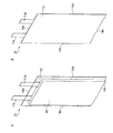
図1Aは、電池セル10の正面側から見た斜視図、図1Bは、その背面側から見た斜視図である。電池セル10は、平面視形状が略矩形であり、当該略矩形の縦横寸法に比べて厚みが薄い薄板形状を有する。この電池セル10では、ラミネートシート13からなる外装内に、略矩形の平面視形状を有する薄板状の発電要素(図示せず)が電解液とともに封入されている。発電要素は、正極集電体の所定領域の両面に正極活物質を含む正極合剤層が塗布形成された正極と、負極集電体の所定領域の両面に負極活物質を含む負極合剤層が塗布形成された負極とが、セパレータを介して交互に積層されてなる電極積層体である。電池の種類は特に制限はないが、二次電池、中でもリチウムイオン二次電池が好ましい。
1A is a perspective view seen from the front side of the
ラミネートシート13は、発電要素に比べて薄く、且つ、可撓性を有している。ラミネートシート13は、例えば、アルミニウム等からなる基層の、発電要素に対向する側の面に熱融着性樹脂層(例えば変性ポリオレフィン層)が積層された可撓性を有する多層シートであってもよい。1枚の矩形のラミネートシート13が、発電要素を挟むように下辺(一方の短辺)14bで二つ折りにされ、下辺14b以外の三辺に沿って重ね合わされてヒートシール法などによりシールされている。
The
下辺14bに対向する上辺(他方の短辺)14aから、正極タブ11p及び負極タブ11nが導出されている。正極タブ11p及び負極タブ11nは、短冊形状を有し、上辺14aに対して直交する方向(即ち、上辺14aに隣接する一対の側辺(長辺)14sと平行な方向)に沿って延びている。正極タブ11pは、例えばアルミニウムの薄板からなり、発電要素を構成する複数の正極集電体(図示せず)と電気的に接続されている。また、負極タブ11nは、例えば銅の薄板、ニッケルメッキされた銅の薄板、または銅/ニッケルのクラッド材等からなり、発電要素を構成する複数の負極集電体(図示せず)と電気的に接続されている。
A
図1Aに示されているように、発電要素に対応する長方形の領域16が電池セル10の三辺14a,14s,14sに沿ったラミネートシート13のシール領域に対して突出している。領域16が突出した面を、電池セル10の「正面」と呼ぶ。一方、図1Bに示されているように、略一平面をなす、正面とは反対側の面を、電池セル10の「裏面」と呼ぶ。
As shown in FIG. 1A, a
本発明において、電池セルの構成は上記に限定されない。例えば、発電要素を2枚の矩形状のラミネートシートで挟み、4辺に沿って2枚のラミネートシートをシールした四方シールタイプの電池セルであってもよい。 In the present invention, the configuration of the battery cell is not limited to the above. For example, a battery cell of a four-side seal type in which a power generation element is sandwiched between two rectangular laminate sheets and two laminate sheets are sealed along four sides may be used.
<電池積層体>
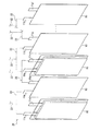
図2は、本発明の一実施形態にかかる電池パックを構成する電池積層体20の分解斜視図である。電池積層体20は、複数の電池セル10が積層されて構成される。電池セル10が積層される方向(図2において横方向)を「積層方向」と呼ぶ。
<Battery laminate>
FIG. 2 is an exploded perspective view of the
図2に示されているように、複数の電池セル10は、隣り合う2つの電池セル10間において異極のタブ(即ち正極タブ11pと負極タブ11n)同士が積層方向に互いに対向するように、1つおきの電池セル10は裏返されている。二点鎖線23で示すように、積層方向に対向する正極タブ11pと負極タブ11nとが電気的に接続される。その結果、複数の電池セル10が直列に接続される。互いに接続された正極タブ11pと負極タブ11nに電圧監視用の配線22が接続される。異極タブと接続されない両端の正極タブ11p’及び負極タブ11n’は、電池積層体20に対して電力の入出力を行う入出力タブとなる。
As shown in FIG. 2, the plurality of
積層方向に隣り合う電池セル10は、例えば両面粘着テープを用いて一体化される。隣り合う電池セル10間に、薄い板材(図示せず)を介在させてもよい。電池積層体20を構成する電池セル10の数は任意である。
The
<電池パック>
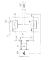
図3は、本発明の一実施形態にかかる電池パック1の概略構成を示したブロック図である。
<Battery pack>
FIG. 3 is a block diagram showing a schematic configuration of the battery pack 1 according to the embodiment of the present invention.
電池積層体20に接続された電圧監視用の複数の配線22(図2参照)は、電圧監視部3に接続されている。
A plurality of voltage monitoring wires 22 (see FIG. 2) connected to the
電池積層体20の入出力タブ11p’,11n’は、パワー配線41p,41nを介して、電池パック1に対して電力の入出力を行う外部接続端子42p,42nに接続されている。正極パワー配線41p上には、正極パワー配線41pを断続するスイッチ43が設けられている。一方、負極パワー配線41n上には、負極パワー配線41nを流れる電流を監視する電流監視部44が設けられている。スイッチ43は、正極パワー配線41pの電気的接続を切り替える開閉器と、当該開閉器を駆動するドライバ回路を含む。本実施形態とは異なり、正極パワー配線41p上に電流監視部44が設けられ、負極パワー配線41n上にスイッチ43が設けられていてもよい。正極パワー配線41p及び負極パワー配線41nのいずれか一方に、スイッチ43及び電流監視部44が設けられていてもよい。パワー配線41p,41n、外部接続端子42p,42n、スイッチ43、電流監視部44は、パワー部4を構成する。
The input /
電圧監視部3は、制御部5に接続されている。制御部5は、電圧監視部3からの信号により電池セル10の電圧が異常であることを検知すると、パワー配線41pを遮断する信号をスイッチ43に出力し、電池積層体20と電池パック1に接続された機器との電気的接続を遮断する。
The
電流監視部44も制御部5に接続されている。制御部5は、電流監視部44からの信号によりパワー配線を流れる電流が異常であることを検知すると、パワー配線41pを遮断する信号をスイッチ43に出力し、電池積層体20と電池パック1の外部との電気的接続を遮断する。
The
図示を省略しているが、電圧監視部3、スイッチ43、電流監視部44、制御部5は、それぞれの機能を発揮するために、電池積層体20から電力供給を受ける。
Although not shown, the
図3に示した構成が、実際の電池パック1でどのように具現化されているかを以下に説明する。 How the configuration shown in FIG. 3 is embodied in the actual battery pack 1 will be described below.
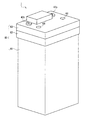
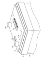
図4は電池パック1の斜視図である。電池パック1は、ケース本体61と、中間枠62と、上蓋63とをこの順に備えたケース60を有している。上蓋63の上面には、電池パック1に対して電力の入出力を行う正極外部接続端子42p及び負極外部接続端子42nが設けられている。
FIG. 4 is a perspective view of the battery pack 1. The battery pack 1 has a
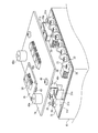
図5は、上蓋63及び中間枠62の内部の構造を透視した電池パック1の主要部の透視斜視図である。ケース本体61は、略直方体形状を有し、上方が開口した有底箱体である。ケース本体61内に電池積層体20(図2参照)が収納されている。ケース本体61の開口を塞ぐように、電圧監視基板73がケース本体61に固定されている。電圧監視基板73の上方に、パワー基板74及び制御基板75が配置されている。図3で説明した電圧監視部3、パワー部4、制御部5は、順に、電圧監視基板73、パワー基板74、制御基板75に設けられている。
FIG. 5 is a perspective view of the main part of the battery pack 1 as seen through the internal structure of the
電圧監視基板73は、略矩形の平面視形状を有する。電圧監視基板73の周囲の4辺のうち、対向する一方の2辺には第1切り欠き31p,31nが形成され、対向する他方の2辺のそれぞれには、複数の第2切り欠き32が形成されている。
The
一対の第1切り欠き31p,31nを通って、電池積層体20の入出力タブ11p’,11n’(図2参照)に接続された短冊状の電極リード21p,21nが、電圧監視基板73の下側(電池積層体20側)から上側に案内されている。電極リード21p,21nは、電圧監視基板73上に搭載された端子台33p,33nに固定されている。短冊状の接続リード45p,45n(図5では正極接続リード45pは見えない)の一端が端子台33p,33nに接続されている。これにより、接続リード45p,45nは、端子台33p,33nを介して電極リード21p,21nと電気的に接続されている。接続リード45p,45nの他端は、パワー基板74に電気的に接続されている(後述する図8を参照)。
The strip-shaped electrode leads 21p and 21n connected to the input /
第2切り欠き32は、電極監視基板73の辺に沿って略一定ピッチで形成されている。端子35が、電極監視基板73上の第2切り欠き32の近傍の位置に搭載されている。端子35は、第2切り欠き32に一対一に対応して複数個設けられている。各第2切り欠き32を通って、電池積層体20に接続された1本の電圧監視用の配線22(図2参照)が、電圧監視基板73の下側(電池積層体20側)から上側に案内されている。配線22は、当該配線22を案内する第2切り欠き32に対応する端子35に接続されている。
The
電圧監視基板73には、電池積層体20を構成する各電池セル10の電圧を監視するための電圧監視回路(例えばIC)36が実装されている。電圧監視回路36は、電圧監視用基板73に形成された配線(図示せず)を介して複数の端子35に接続されている。電圧監視回路36は、各電池セル10の電圧を監視する電圧監視部3(図3参照)を構成する。
On the
パワー基板74は、電圧監視用基板73の上方に、これから離間して配置されている。パワー基板74には、電池パック1に対して電力の入出力を行う外部接続端子42p,42n(図3参照)が搭載されている。接続リード45p,45nと外部接続端子42p,42nとをつなぐパワー配線41p,41n(図3参照、図5では図示を省略)がパワー基板74の表面又はその内部に形成されている。更に、パワー基板74には、スイッチ43(図3参照)を構成するスイッチ回路(例えばIC)43a、及び、電流監視部44(図3参照)を構成する電流監視回路(例えばIC)44aが搭載されている。
The
制御基板75は、パワー基板74の上方に、これから離間して配置されている。制御基板75には、制御部5(図3参照)を構成する制御回路(例えばIC)51が搭載されている。
The
電圧監視基板73、パワー基板74、制御基板75は、柔軟性を有するケーブル(図示せず)で相互に電気的に接続されている。
The
<作用>
本実施形態の電池パック1の作用を、従来の電池パックと比較しながら説明する。
<Action>
The operation of the battery pack 1 of the present embodiment will be described in comparison with a conventional battery pack.
上述したように、近年では、電池パックに対する小型化且つ大容量化の要望が増大している。電池パックの大容量化を実現するためには、電池積層体と外部接続端子とをつなぐパワー配線の電流を増大させる必要がある。これは、パワー配線から発生するノイズを増大させる。従来の電池パックでは、パワー配線と、電圧監視部及び制御部を含む保護回路とが同一の基板上に設けられていたので、パワー配線からのノイズによって電圧監視部及び制御部を構成するデジタル回路に悪影響を及ぼす可能性があった。ノイズの悪影響を回避するためには、パワー配線と電圧監視部及び制御部とを離間する必要があり、これは基板面積の増大を招き、電池パックの小型化を困難にしていた。 As described above, in recent years, there has been an increasing demand for smaller and larger capacity battery packs. In order to increase the capacity of the battery pack, it is necessary to increase the current of the power wiring that connects the battery stack and the external connection terminal. This increases the noise generated from the power wiring. In the conventional battery pack, since the power wiring and the protection circuit including the voltage monitoring unit and the control unit are provided on the same substrate, the digital circuit constituting the voltage monitoring unit and the control unit by noise from the power wiring Could have an adverse effect on In order to avoid the adverse effects of noise, it is necessary to separate the power wiring from the voltage monitoring unit and the control unit, which increases the substrate area and makes it difficult to reduce the size of the battery pack.
これに対して、本実施形態の電池パック1では、パワー配線41p,41nを含むパワー部4が、電圧監視部3が設けられた電圧監視基板73及び制御部5が設けられた制御基板75とは別のパワー基板74に設けられている。従って、パワー部4と電圧監視部3及び制御部5との距離を容易に拡大することができる。また、必要に応じて、パワー部4と電圧監視部3及び制御部5との間にシールドを施すことができる。その結果、パワー部4からのノイズによって電圧監視部3及び制御部5を構成するデジタル回路に悪影響を及ぼす可能性を低減することができる。
On the other hand, in the battery pack 1 of this embodiment, the
基板を分割することにより、各基板に形成する配線や基板に搭載する部品の配置に関する設計の自由度が向上する。これは、単一の基板を用いる従来の構成に比べて、基板全体の小型化に有利である。 By dividing the substrate, the degree of freedom of design related to the arrangement of the wiring formed on each substrate and the components mounted on the substrate is improved. This is advantageous for downsizing the entire substrate as compared to the conventional configuration using a single substrate.
電池パックの基板としては、その表面及び内部に複数層の配線(配線パターン)が所定パターンで形成された、いわゆる多層基板が一般的に用いられる。多層基板では、通常、各層の配線の厚さ(基板の表面に垂直な方向に沿った寸法)は同一である。従来の電池パックでは、パワー配線と、電圧監視部及び制御部を含む保護回路とが同一の基板上に設けられていた。パワー配線の大電流化のために配線が厚い多層基板を用いた場合には、そのような厚い配線は電圧監視部及び制御部には無駄になり、また、多層基板が厚肉化する。一方、パワー配線の大電流化のために配線が広幅の多層基板を用いた場合には、基板面積の増大を招く。 As the substrate of the battery pack, a so-called multilayer substrate in which a plurality of layers of wiring (wiring patterns) are formed in a predetermined pattern on the surface and inside is generally used. In a multilayer substrate, the thickness of wiring in each layer (the dimension along the direction perpendicular to the surface of the substrate) is usually the same. In the conventional battery pack, the power wiring and the protection circuit including the voltage monitoring unit and the control unit are provided on the same substrate. When a multilayer substrate with thick wiring is used to increase the current of the power wiring, such a thick wiring is wasted in the voltage monitoring unit and the control unit, and the multilayer substrate becomes thick. On the other hand, when a multilayer substrate with a wide wiring is used to increase the current of the power wiring, the substrate area increases.
これに対して、本実施形態の電池パック1では、パワー配線41p,41nを含むパワー部4が、電圧監視部3が設けられた電圧監視基板73及び制御部5が設けられた制御基板75とは別のパワー基板74に設けられている。従って、各基板73,74,75として、最適な多層基板を用いることができる。例えば、パワー配線41p,41nの大電流化のために、パワー基板74として、配線の厚さが厚い多層基板を用いることができる。これにより、配線の幅(基板の表面に平行な方向に沿った寸法)の増大を抑えることができるので、基板面積の増大を回避できる。一方、大電流が必要とされない電圧監視基板73及び制御基板75としては、配線の厚さ及び幅が相対的に小さな多層基板を用いることができる。これにより、基板73,75を薄く且つ小面積化することができる。一実施例では、パワー基板74として、厚さが300μmの配線が形成された、全体厚さが2.3mmの多層基板を用いることができ、電圧監視用基板73として、厚さが35μmの配線が形成された、全体厚さが1.5mmの2層基板を用いることができ、制御基板75として、厚さが35μmの配線が形成された、全体厚さが1.5mmの6層基板を用いることができる。
On the other hand, in the battery pack 1 of this embodiment, the
以上のように、本実施形態によれば、パワー部4が電圧監視部3及び制御部5が設けられた基板73,75とは別のパワー基板74に設けられており、且つ、パワー基板74に形成された配線は、電圧監視部3及び制御部5が設けられた基板73,75に形成された配線より厚い。これにより、電池パック1の小型化且つ大容量化を実現することができる。
As described above, according to the present embodiment, the
更に、3つの基板73,74,75を積層することにより、上述したノイズの問題を回避しながら、基板73,74,75を全体として小型化することができる。なお、基板73,74,75の積層順序は上記の実施形態に限定されず、任意に変更することができる。
Further, by stacking the three
また、保護回路を機能に着目して複数部分に分割してそれぞれを別個の基板に搭載したことにより、保護回路の各部分をモジュール化することができる。これにより、保護回路を構成する複数の基板のうちの一部のみを設計変更したり入れ替えたりすることが容易になるので、電池パックの多品種化に容易に対応できる。また、保護回路の修理も、一部の基板のみを交換することで行うことができる。 Further, the protection circuit is divided into a plurality of parts with attention paid to the function, and each part is mounted on a separate substrate, whereby each part of the protection circuit can be modularized. As a result, it becomes easy to change the design or replace only a part of the plurality of substrates constituting the protection circuit, so that it is possible to easily cope with a wide variety of battery packs. Further, the protection circuit can be repaired by exchanging only a part of the substrates.
<電池積層体とパワー配線との接続>
電池パック1を組み立てる際には、いずれかの段階で、電池積層体20の入出力タブ11p’,11n’(図2参照)とパワー配線41p,41n(図3参照)とを電気的に接続する工程(以下「電池−パワー基板接続工程」という)を行う必要がある。電池−パワー基板接続工程を早い段階で行うと、その後の組み立て工程で感電や短絡などの事故が生じる可能性が高くなる。電池積層体20の容量(電圧)が高い場合には、そのような事故による損害は甚大となり得る。更に、本実施形態のように、複数の基板を用いる場合には、電池パック1の組み立て工程が複雑になるので、そのような事故が発生する可能性は高い。
<Connection between battery stack and power wiring>
When the battery pack 1 is assembled, the input /
本実施形態の電池パック1では、このような事故が生じる可能性を低減する構造が採用されている。これを以下に説明する。 In the battery pack 1 of the present embodiment, a structure that reduces the possibility of such an accident is employed. This will be described below.
本実施形態の電池パック1は、概略、以下の工程を順に経て組み立てられる。即ち、(1)ケース本体61に電池積層体20を収納する。(2)ケース本体61に電圧監視基板73を固定し、電池積層体20と電圧監視基板73とを結線する。(3)ケース本体61に中間枠62を固定する。(4)中間枠62にパワー基板74を固定する。(5)制御基板75を装着した上蓋63を中間枠62に固定する。
The battery pack 1 of the present embodiment is generally assembled through the following steps in order. (1) The
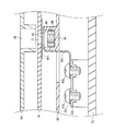
図6は、上記の組み立てにおいて、中間枠62にパワー基板74を固定した状態(上記工程(4))を示した斜視図である。この後、パワー基板74を覆うように、上蓋63を中間枠62に固定する(上記工程(5))。図7は、上蓋63を固定した状態を示した、図6の7−7線を含む上下方向面に相当する断面に沿った矢視断面図である。図7では、図面を簡単化するために、断面より後ろに見える部材を省略している。
FIG. 6 is a perspective view showing a state in which the
図7に示されているように、電圧監視基板73に導電性を有する端子台33nが搭載されている。電池積層体20の入出力タブ11n’(図2参照)に接続された電極リード21nが、端子台33nにネジ47aで密着固定されている。略Z字上に折り曲げられた接続リード45nの下端が、端子台33nにネジ47bで密着固定されている。従って、端子台33nを介して、電極リード21nと接続リード45nとが電気的に接続されている。なお、端子台33nが絶縁性を有していてもよく、その場合には、端子台33nの上面に導電層を形成して、当該導電層を介して電極リード21nと接続リード45nとを電気的に接続することができる。
As shown in FIG. 7, a
中間枠62は、端子台33nの近傍に、保持部65を有している。保持部65は、上方が開口した有底箱形状を有し、その内部のキャビティ66内にナット48を保持している。キャビティ66内において、ナット48は上下方向(パワー基板74に接離する方向)に移動可能である。接続リード45nの上端は、保持部65の開口を塞ぐように、水平方向に延びている。接続リード45nの上端には、ナット48と略同軸となる位置に、接続リード45nを貫通する貫通孔46が形成されている。更に、パワー基板74にも、ナット48と略同軸となる位置に、パワー基板74を貫通する貫通孔77が形成されている。パワー基板74の下面であって、接続リード45nの上端に対向する領域には、導電性金属からなる配線端子41tが形成されている。配線端子41tは、貫通孔77の開口を取り囲んでいる。配線端子41tは、パワー配線41n(図3参照)の一部をなす。接続リード45nと配線端子41tとは離間している。上蓋63がパワー基板74を覆っている。上蓋63の、ナット48と略同軸となる位置に、上蓋63を貫通する貫通孔68が形成されている。
The
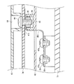
電池積層体20の入出力タブ11n’とパワー配線41nとを接続する電池−パワー基板接続工程を行う際には、上蓋63に形成された貫通孔68に、上方からネジ49を挿入する(図8参照)。ネジ49を、上蓋63の貫通孔68、パワー基板74の貫通孔77、接続リード45nの貫通孔46を順に貫通させて、保持部65に保持されたナット48と螺合させる。ナット48の外周の正六角柱面が、保持部65のキャビティ66の内周面に当接するので、ナット48の回転が阻止される。ネジ49とナット48との螺合が進むにしたがってナット48が上方に持ち上げられ、これにともない接続リード45nも持ち上げられる。そして、遂に、図8に示すように、ネジ49とナット48とがしっかりと締結される。これにより、接続リード45nとパワー配線41nの配線端子41tとが密着して電気的に接続され、電池−パワー基板接続工程が完了する。
When performing the battery-power board connecting step of connecting the input /
上記の説明は、電池積層体20の入出力タブとパワー配線との負極側の電気的接続に関するものであるが、正極側の電気的接続も上記と同様である。
The above description relates to the electrical connection on the negative electrode side between the input / output tab of the
このように、本実施形態では、上蓋63を中間枠62に取り付けただけでは、電池積層体20の入出力タブ11p’,11n’と導通した接続リード45p,45nとパワー配線41p,41nとは、電気的に接続されない。上蓋63の上方から、貫通孔68にネジ49を挿入して、パワー基板74の下側に保持されたナット48に螺合することによって、電池−パワー基板接続工程が完了する。本実施形態によれば、基板73,74,75を、電池積層体20の入出力タブ11p’,11n’に電気的に接続されていない状態で組み付けることができる。電池−パワー基板接続工程は、上蓋63を固定した後、即ち、電池パック1の組み立て作業の最終工程として行う。その結果、基板73,74,75の組み付け作業において感電や短絡などの事故が生じる可能性を低減することができる。上蓋63の貫通孔68は、電池−パワー基板接続工程を行った後、必要に応じて、上蓋63にラベルを貼付したり、貫通孔68に栓を挿入したりして塞いでもよい。
Thus, in the present embodiment, the connection leads 45p and 45n and the
本実施形態では、ナット48は、ネジ49と螺合する前に、保持部65のキャビティ66内に上下方向に移動可能に保持されている。この構成では、中間枠62にパワー基板74を取り付ける前に、ナット48を保持部65のキャビティ66内に収納しておけばよい。ナット48が保持部65に保持されているので、ネジ49をパワー基板74の貫通孔77に挿入して回転させれば、ネジ49とナット48とを簡単に螺合させることができる。これにより、電池−パワー基板接続工程を効率よく行うことができる。
In this embodiment, the
上記の実施形態は、例示にすぎない。本発明は、上記の実施形態に限定されず種々に変更することができる。 The above embodiments are merely examples. The present invention is not limited to the above embodiment and can be variously modified.
例えば、上記の実施形態では、電圧監視部3と制御部5とが上下方向に積層されていたが、これらが同一水平面に沿って配置されていてもよい。電圧監視部3及び制御部5を、別個の基板に設けるのではなく、共通する基板に設けてもよい。また、電圧監視部3、パワー部4、制御部5のうちの少なくとも一つが、2以上に分割されてそれぞれ別個の基板に設けられていてもよい。
For example, in the above-described embodiment, the
上記の実施形態では、電池積層体20の入出力タブ11p’,11n’は、電極リード21p,21n及び接続リード45p,45nを介してパワー配線41p,41nに接続されていたが、電極リード21p,21n及び接続リード45p,45nのうちの一方又は両方を省略してもよい。あるいは、入出力タブ11p’,11n’とパワー配線41p,41nとの間に、これら以外の部材を更に介在させてもよい。
In the above embodiment, the input /
上記の実施形態では、入出力タブ11p’,11n’とパワー配線41p,41nとの間に、電圧監視基板73に設けた端子台33p,33nが介在していたが、端子台33p,33nを省略し、電極リード21p,21n(または入出力タブ11p’,11n’と導通した任意のリード)をパワー基板74のパワー配線41p,41nに接続してもよい。
In the above embodiment, the terminal blocks 33p and 33n provided on the
ナット48を保持する保持部65は、中間枠62に設けられている必要はない。例えば、電圧監視基板73又はパワー基板74に、保持部65を設けてもよい。保持部65を省略し、作業者がナット48を保持しながらナット48とネジ49とを螺合させてもよい。
The holding
電池パックの保護回路が、電池セルの温度を監視する温度監視部を更に備えていてもよい。この場合、制御部5は、温度監視部からの信号により電池セルの温度が異常であることを検知すると、パワー配線を遮断する信号をスイッチ43に出力し、電池積層体20と電池パック1の外部との電気的接続を遮断するように構成することができる。このような温度監視部は、パワー基板74以外の基板に設けることが好ましい。
The protection circuit of the battery pack may further include a temperature monitoring unit that monitors the temperature of the battery cell. In this case, when the
ケースの構成は、上記の実施形態に限定されず、任意である。例えば中間枠62を省略してもよい。
The configuration of the case is not limited to the above embodiment, and is arbitrary. For example, the
上蓋63が、ネジ49を挿入するための貫通孔68を有していなくてもよい。この場合、電池−パワー基板接続工程は、上蓋63を中間枠62に固定する工程(上記の工程(5))の直前に行うことができる。この場合も、接続リード45p,45nとパワー配線41p,41nとの接続を除いて、電池パック1の組み立てにおいて必要な全ての電気的接続を終了した後に、電池−パワー基板接続工程を行うことができる。これにより、電池−パワー基板接続工程の直前まで、基板73,74,75を、電池積層体20の入出力タブ11p’,11n’に電気的に接続されていない状態で組み付けることができる。その結果、基板73,74,75の組み付け作業において感電や短絡などの事故が生じる可能性を低減することができる。
The
上記の実施形態では、制御基板75は、上蓋63に装着される。但し、本発明はこれに限定されず、制御基板75がパワー基板74に固定されるように構成されていてもよい。この場合、制御基板75をパワー基板74に固定した後、上蓋63を、制御基板75及びパワー基板74を覆うように固定枠62に固定する。
In the above embodiment, the
上記の説明では、上蓋63側を電池パック1の上側、ケース本体61側を電池パック1の下側として、電池パック1の上下方向及び水平方向を記載したが、これは説明の便宜にすぎない。電池パックの実際の使用時の向きはこれに限定されない。
In the above description, the upper and lower directions and the horizontal direction of the battery pack 1 are described with the
本発明の利用分野は特に制限はなく、自動車、バイク、電動アシスト自転車等の各種移動機器、携帯情報端末、無停電電源装置(UPS)、蓄電装置等の電源に使用される電池パックとして広範囲に利用することができる。 The field of application of the present invention is not particularly limited, and is widely used as a battery pack used as a power source for various mobile devices such as automobiles, motorcycles, and electrically assisted bicycles, personal digital assistants, uninterruptible power supplies (UPS), and power storage devices. Can be used.
1 電池パック
3 電圧監視部
4 パワー部
5 制御部
10 電池セル
11p’,11n’ 入出力タブ
20 電池積層体
22 電圧監視用の配線
41p,41n パワー配線
42p,42n 外部接続端子
43 スイッチ
44 電流監視部
45p,45n 接続リード(リード)
48 ナット
49 ネジ
63 上蓋
65 保持部(保持機構)
66 キャビティ
68 貫通孔
73 電圧監視基板
74 パワー基板
75 制御基板
DESCRIPTION OF SYMBOLS 1
48
66
Claims (5)
前記電池積層体と外部接続端子とをつなぐパワー配線が設けられたパワー基板とを備え、
前記電池積層体の入出力タブと電気的に接続されたリードが前記パワー基板に対向し、
ネジが、前記パワー基板及び前記リードをこの順に貫通し、前記リードに対して前記パワー基板とは反対側に配置されたナットと螺合しており、これにより、前記リードが前記パワー基板に形成された前記パワー配線に電気的に接続されていることを特徴とする電池パック。 A battery stack in which a plurality of thin battery cells are stacked and the plurality of battery cells are connected in series;
A power board provided with a power wiring connecting the battery laminate and the external connection terminal,
The lead electrically connected to the input / output tab of the battery stack is opposed to the power board,
A screw penetrates the power board and the lead in this order and is screwed with a nut disposed on the opposite side of the power board to the lead, whereby the lead is formed on the power board. A battery pack, wherein the battery pack is electrically connected to the power wiring.
前記上蓋に、前記ネジを挿入するための貫通孔が形成されている請求項1〜4のいずれかに記載の電池パック。 Further comprising an upper lid covering the power substrate,
The battery pack according to claim 1, wherein a through hole for inserting the screw is formed in the upper lid.
Priority Applications (1)
| Application Number | Priority Date | Filing Date | Title |
|---|---|---|---|
| JP2017126380A JP6327770B2 (en) | 2017-06-28 | 2017-06-28 | Battery pack |
Applications Claiming Priority (1)
| Application Number | Priority Date | Filing Date | Title |
|---|---|---|---|
| JP2017126380A JP6327770B2 (en) | 2017-06-28 | 2017-06-28 | Battery pack |
Related Parent Applications (1)
| Application Number | Title | Priority Date | Filing Date |
|---|---|---|---|
| JP2013176961A Division JP6190213B2 (en) | 2013-08-28 | 2013-08-28 | Battery pack |
Publications (2)
| Publication Number | Publication Date |
|---|---|
| JP2017168464A JP2017168464A (en) | 2017-09-21 |
| JP6327770B2 true JP6327770B2 (en) | 2018-05-23 |
Family
ID=59910004
Family Applications (1)
| Application Number | Title | Priority Date | Filing Date |
|---|---|---|---|
| JP2017126380A Active JP6327770B2 (en) | 2017-06-28 | 2017-06-28 | Battery pack |
Country Status (1)
| Country | Link |
|---|---|
| JP (1) | JP6327770B2 (en) |
Families Citing this family (1)
| Publication number | Priority date | Publication date | Assignee | Title |
|---|---|---|---|---|
| JP7771823B2 (en) * | 2022-03-14 | 2025-11-18 | トヨタ自動車株式会社 | Battery case |
Family Cites Families (6)
| Publication number | Priority date | Publication date | Assignee | Title |
|---|---|---|---|---|
| JP4632353B2 (en) * | 2005-03-08 | 2011-02-16 | エルナー株式会社 | Storage element connection structure and storage element module |
| JP4539763B2 (en) * | 2008-06-13 | 2010-09-08 | トヨタ自動車株式会社 | electrode |
| JP5340676B2 (en) * | 2008-08-29 | 2013-11-13 | 三洋電機株式会社 | Battery system |
| JP5646046B2 (en) * | 2011-04-04 | 2014-12-24 | 日立オートモティブシステムズ株式会社 | Power storage module |
| JP2013084368A (en) * | 2011-10-06 | 2013-05-09 | Auto Network Gijutsu Kenkyusho:Kk | Battery module |
| JP2013114782A (en) * | 2011-11-25 | 2013-06-10 | Sanyo Electric Co Ltd | Battery pack |
-
2017
- 2017-06-28 JP JP2017126380A patent/JP6327770B2/en active Active
Also Published As
| Publication number | Publication date |
|---|---|
| JP2017168464A (en) | 2017-09-21 |
Similar Documents
| Publication | Publication Date | Title |
|---|---|---|
| JP6190213B2 (en) | Battery pack | |
| JP6141732B2 (en) | Battery stack and battery pack | |
| JP6233891B2 (en) | Power storage device | |
| JP4457812B2 (en) | Battery pack and module battery | |
| EP4191780B1 (en) | Battery module including multiple parallel battery cells | |
| JP6222713B2 (en) | Bus bar structure and power conversion device using bus bar structure | |
| JP5374979B2 (en) | Batteries and batteries | |
| US20140141309A1 (en) | Battery module | |
| US11942647B2 (en) | Harness isolation plate assembly, battery module, battery pack and device | |
| WO2013011748A1 (en) | Battery module | |
| CN116097516A (en) | Battery module, battery pack including the same, and method of manufacturing the same | |
| WO2018062226A1 (en) | Battery module, and battery pack | |
| CN112787043B (en) | Battery module and electrical device | |
| KR20220089648A (en) | Power storage module | |
| JP6327770B2 (en) | Battery pack | |
| WO2013011750A1 (en) | Battery module | |
| JP6101158B2 (en) | Battery pack | |
| US20140141321A1 (en) | Battery module | |
| US20150207178A1 (en) | Battery module | |
| JP4977356B2 (en) | Electrical device assembly | |
| JP2005340016A (en) | Film-clad electrical device module and assembled battery system | |
| KR102954205B1 (en) | Battery module and battery pack including the same | |
| KR20190000047U (en) | A connection structure of pouch type battery | |
| JP6081866B2 (en) | Battery pack | |
| WO2022230435A1 (en) | Power storage device |
Legal Events
| Date | Code | Title | Description |
|---|---|---|---|
| A621 | Written request for application examination |
Free format text: JAPANESE INTERMEDIATE CODE: A621 Effective date: 20170718 |
|
| A977 | Report on retrieval |
Free format text: JAPANESE INTERMEDIATE CODE: A971007 Effective date: 20180406 |
|
| TRDD | Decision of grant or rejection written | ||
| A01 | Written decision to grant a patent or to grant a registration (utility model) |
Free format text: JAPANESE INTERMEDIATE CODE: A01 Effective date: 20180412 |
|
| A61 | First payment of annual fees (during grant procedure) |
Free format text: JAPANESE INTERMEDIATE CODE: A61 Effective date: 20180416 |
|
| R150 | Certificate of patent or registration of utility model |
Ref document number: 6327770 Country of ref document: JP Free format text: JAPANESE INTERMEDIATE CODE: R150 |
|
| R250 | Receipt of annual fees |
Free format text: JAPANESE INTERMEDIATE CODE: R250 |
|
| S533 | Written request for registration of change of name |
Free format text: JAPANESE INTERMEDIATE CODE: R313533 |
|
| R350 | Written notification of registration of transfer |
Free format text: JAPANESE INTERMEDIATE CODE: R350 |
|
| R250 | Receipt of annual fees |
Free format text: JAPANESE INTERMEDIATE CODE: R250 |
|
| R250 | Receipt of annual fees |
Free format text: JAPANESE INTERMEDIATE CODE: R250 |
|
| R250 | Receipt of annual fees |
Free format text: JAPANESE INTERMEDIATE CODE: R250 |
|
| R250 | Receipt of annual fees |
Free format text: JAPANESE INTERMEDIATE CODE: R250 |