JP6324324B2 - Image pickup apparatus having dummy pattern - Google Patents
Image pickup apparatus having dummy pattern Download PDFInfo
- Publication number
- JP6324324B2 JP6324324B2 JP2015000093A JP2015000093A JP6324324B2 JP 6324324 B2 JP6324324 B2 JP 6324324B2 JP 2015000093 A JP2015000093 A JP 2015000093A JP 2015000093 A JP2015000093 A JP 2015000093A JP 6324324 B2 JP6324324 B2 JP 6324324B2
- Authority
- JP
- Japan
- Prior art keywords
- dummy pattern
- microlens
- imaging device
- microlens structure
- passivation film
- Prior art date
- Legal status (The legal status is an assumption and is not a legal conclusion. Google has not performed a legal analysis and makes no representation as to the accuracy of the status listed.)
- Active
Links
Images
Classifications
-
- H—ELECTRICITY
- H10—SEMICONDUCTOR DEVICES; ELECTRIC SOLID-STATE DEVICES NOT OTHERWISE PROVIDED FOR
- H10F—INORGANIC SEMICONDUCTOR DEVICES SENSITIVE TO INFRARED RADIATION, LIGHT, ELECTROMAGNETIC RADIATION OF SHORTER WAVELENGTH OR CORPUSCULAR RADIATION
- H10F39/00—Integrated devices, or assemblies of multiple devices, comprising at least one element covered by group H10F30/00, e.g. radiation detectors comprising photodiode arrays
- H10F39/80—Constructional details of image sensors
- H10F39/805—Coatings
-
- H—ELECTRICITY
- H10—SEMICONDUCTOR DEVICES; ELECTRIC SOLID-STATE DEVICES NOT OTHERWISE PROVIDED FOR
- H10F—INORGANIC SEMICONDUCTOR DEVICES SENSITIVE TO INFRARED RADIATION, LIGHT, ELECTROMAGNETIC RADIATION OF SHORTER WAVELENGTH OR CORPUSCULAR RADIATION
- H10F39/00—Integrated devices, or assemblies of multiple devices, comprising at least one element covered by group H10F30/00, e.g. radiation detectors comprising photodiode arrays
- H10F39/011—Manufacture or treatment of image sensors covered by group H10F39/12
- H10F39/024—Manufacture or treatment of image sensors covered by group H10F39/12 of coatings or optical elements
-
- H—ELECTRICITY
- H10—SEMICONDUCTOR DEVICES; ELECTRIC SOLID-STATE DEVICES NOT OTHERWISE PROVIDED FOR
- H10F—INORGANIC SEMICONDUCTOR DEVICES SENSITIVE TO INFRARED RADIATION, LIGHT, ELECTROMAGNETIC RADIATION OF SHORTER WAVELENGTH OR CORPUSCULAR RADIATION
- H10F39/00—Integrated devices, or assemblies of multiple devices, comprising at least one element covered by group H10F30/00, e.g. radiation detectors comprising photodiode arrays
- H10F39/80—Constructional details of image sensors
- H10F39/805—Coatings
- H10F39/8053—Colour filters
-
- H—ELECTRICITY
- H10—SEMICONDUCTOR DEVICES; ELECTRIC SOLID-STATE DEVICES NOT OTHERWISE PROVIDED FOR
- H10F—INORGANIC SEMICONDUCTOR DEVICES SENSITIVE TO INFRARED RADIATION, LIGHT, ELECTROMAGNETIC RADIATION OF SHORTER WAVELENGTH OR CORPUSCULAR RADIATION
- H10F39/00—Integrated devices, or assemblies of multiple devices, comprising at least one element covered by group H10F30/00, e.g. radiation detectors comprising photodiode arrays
- H10F39/80—Constructional details of image sensors
- H10F39/806—Optical elements or arrangements associated with the image sensors
- H10F39/8063—Microlenses
-
- G—PHYSICS
- G02—OPTICS
- G02B—OPTICAL ELEMENTS, SYSTEMS OR APPARATUS
- G02B3/00—Simple or compound lenses
- G02B3/0006—Arrays
-
- G—PHYSICS
- G02—OPTICS
- G02B—OPTICAL ELEMENTS, SYSTEMS OR APPARATUS
- G02B5/00—Optical elements other than lenses
- G02B5/20—Filters
- G02B5/201—Filters in the form of arrays
Landscapes
- Solid State Image Pick-Up Elements (AREA)
- Transforming Light Signals Into Electric Signals (AREA)
- Color Television Image Signal Generators (AREA)
Description
本発明は、撮像装置に関するものであって、特に、パッシベーション膜の剥離を防止するダミーパターンを有する撮像装置に関するものである。 The present invention relates to an imaging apparatus, and more particularly to an imaging apparatus having a dummy pattern for preventing the passivation film from peeling off.
画像センサーは、すでに、幅広く、各種画像取得装置、たとえば、ビデオカメラ、デジタルカメラ等に用いられている。一般に、ソリッドステートの撮像装置、たとえば、電荷結合素子(CCD)センサーや相補型MOS(CMOS)センサーは、光電子のトランスデューサー、たとえば、フォトダイオードを有し、光線を電荷に変換する。フォトダイオードは半導体基板、たとえば、シリコンチップ上に形成される。フォトダイオード中に生成される光電子に対応する信号電荷は、CCD−型またはCMOS−型の読み取り回路により得られる。 Image sensors are already widely used in various image acquisition devices such as video cameras and digital cameras. In general, solid-state imaging devices, such as charge coupled device (CCD) sensors and complementary MOS (CMOS) sensors, have optoelectronic transducers, such as photodiodes, that convert light into charges. The photodiode is formed on a semiconductor substrate, for example, a silicon chip. The signal charge corresponding to the photoelectrons generated in the photodiode is obtained by a CCD-type or CMOS-type reading circuit.
ソリッドステートの撮像装置において、フォトダイオードが、画素アレイ中に設置される。このほか、ソリッドステートの撮像装置は、フォトダイオードの上に設置されるマイクロレンズアレイを有する。マイクロレンズアレイの各マイクロレンズ素子は、各画素で、対応するフォトダイオードに照準されている。保護膜がマイクロレンズアレイ上に形成されて、撮像装置のパッケージプロセスで、ウェハから個々のチップを切断するなどの後続の工程段階で、マイクロレンズ素子を保護する。 In a solid-state imaging device, a photodiode is installed in a pixel array. In addition, the solid-state imaging device has a microlens array installed on the photodiode. Each microlens element of the microlens array is aimed at a corresponding photodiode in each pixel. A protective film is formed on the microlens array to protect the microlens elements in subsequent process steps such as cutting individual chips from the wafer in the packaging process of the imaging device.
ある撮像装置において、パッシベーション膜が、保護のために、マイクロレンズ構造上に形成される。撮像装置の基板が、研磨プロセスにより薄くされるとき、テープは、通常、パッシベーション膜に取り付けられて、撮像装置を保護する。基板が薄くされた後、テープが撮像装置から除去される。しかし、テープの除去は、パッシベーション膜の剥離を生じる。パッシベーション膜剥離問題は、不都合なほどに、撮像装置のパッケージ歩留まりを減少させる。 In some imaging devices, a passivation film is formed on the microlens structure for protection. When the substrate of the imaging device is thinned by a polishing process, a tape is usually attached to the passivation film to protect the imaging device. After the substrate is thinned, the tape is removed from the imaging device. However, removal of the tape causes peeling of the passivation film. The passivation film delamination problem undesirably reduces the package yield of the imaging device.
本発明は、ダミーパターンを有する撮像装置を提供し、パッシベーション膜の剥離を防止することを目的とする。 An object of the present invention is to provide an imaging device having a dummy pattern, and to prevent the passivation film from peeling off.
本発明の実施態様によると、撮像装置の各種ダミーパターン構造設計は、テープとダミーパターン上に設置されたパッシベーション膜間の接触面積を減少させることができる。よって、テープが除去されるとき、本発明のダミーパターン構造設計により、パッシベーション膜剥離問題が克服される。 According to the embodiment of the present invention, various dummy pattern structure designs of the image pickup apparatus can reduce the contact area between the tape and the passivation film installed on the dummy pattern. Thus, when the tape is removed, the passivation pattern peeling problem is overcome by the dummy pattern structure design of the present invention.
本発明の複数の実施態様において、撮像装置が提供される。撮像装置は、アクティブ領域内の基板上に形成される複数の光電変換素子を有する。マイクロレンズ構造が、さらに、光電変換素子上に設置される。このほか、ダミーパターンが、アクティブ領域を囲む周辺領域内に基板上に設置される。さらに、パッシベーション膜が、共形で、マイクロレンズ構造とダミーパターン上に形成される。ダミーパターンの上部に形成されるパッシベーション膜は、マイクロレンズの外側の周辺領域の表面積より小さい表面積を有する。 In embodiments of the present invention, an imaging device is provided. The imaging device has a plurality of photoelectric conversion elements formed on a substrate in the active region. A microlens structure is further installed on the photoelectric conversion element. In addition, a dummy pattern is placed on the substrate in the peripheral area surrounding the active area. In addition, a passivation film is conformally formed on the microlens structure and the dummy pattern. The passivation film formed on the dummy pattern has a surface area smaller than the surface area of the peripheral region outside the microlens.
複数の実施態様において、ダミーパターンは、複数の突起素子を有する。各突起素子は、凸状、円柱状、角柱状、円錐または角錐状を含む形状を有する。 In a plurality of embodiments, the dummy pattern has a plurality of protruding elements. Each protruding element has a shape including a convex shape, a cylindrical shape, a prism shape, a cone shape, or a pyramid shape.
複数の実施態様において、ダミーパターンは、凸状の突起素子から構成される。凸状の突起素子は、マイクロレンズ構造の各マイクロレンズ素子の形状と同じ形状を有する。さらに、ダミーパターンの凸状の突起素子は、マイクロレンズ構造と同じ高さである。 In a plurality of embodiments, the dummy pattern is composed of convex projecting elements. The convex projecting element has the same shape as each microlens element of the microlens structure. Furthermore, the convex protrusion elements of the dummy pattern are the same height as the microlens structure.
複数の実施態様において、ダミーパターン上部は、マイクロレンズ構造の上部より低いか、または、高い。 In some embodiments, the upper portion of the dummy pattern is lower or higher than the upper portion of the microlens structure.
複数の実施態様において、ダミーパターン上部のパッシベーション膜は、マイクロレンズ構造とダミーパターンを被覆するテープと接触する。複数の実施態様において、ダミーパターン上部のパッシベーション膜の表面積は、マイクロレンズ構造の外側の周辺領域の表面積の約50−80%である。 In some embodiments, the passivation film over the dummy pattern is in contact with the microlens structure and the tape covering the dummy pattern. In some embodiments, the surface area of the passivation film above the dummy pattern is about 50-80% of the surface area of the peripheral region outside the microlens structure.
複数の実施態様において、撮像装置は、さらに、マイクロレンズ構造と光電変換素子間に設置されるフィルター層を有する。カラーフィルター層は、周辺領域内に設置される延長部分を有する。ダミーパターンは、カラーフィルター層の延長部分上に設置される。 In some embodiments, the imaging device further includes a filter layer disposed between the microlens structure and the photoelectric conversion element. The color filter layer has an extended portion installed in the peripheral region. The dummy pattern is installed on the extended portion of the color filter layer.
複数の実施態様において、マイクロレンズ構造は、アクティブ領域から周辺領域に延伸し、ダミーパターンと接触する部分を有する。複数の実施態様において、マイクロレンズ構造は、ダミーパターンにより囲まれる。 In embodiments, the microlens structure has a portion extending from the active region to the peripheral region and in contact with the dummy pattern. In embodiments, the microlens structure is surrounded by a dummy pattern.
複数の実施態様において、ダミーパターンは、周辺領域内に規則的に設置される。周辺領域は、ダミーパターンにより完全に占有される。別の実施態様において、ダミーパターンは、周辺領域でランダムに設置される。周辺領域の一部は、ダミーパターンにより占有されない。 In some embodiments, the dummy patterns are regularly arranged in the peripheral area. The peripheral area is completely occupied by the dummy pattern. In another embodiment, the dummy pattern is randomly placed in the peripheral area. A part of the peripheral area is not occupied by the dummy pattern.
複数の実施態様において、ダミーパターンの材料は、マイクロレンズ構造の材料と同じである。複数の実施態様において、パッシベーション膜の材料は、化学気相堆積により形成される酸化ケイ素を含む。 In embodiments, the material of the dummy pattern is the same as the material of the microlens structure. In embodiments, the passivation film material comprises silicon oxide formed by chemical vapor deposition.
本発明のダミーパターン設計により、パッシベーション膜剥離問題を克服し、よって、撮像装置の歩留まりが増加する。さらに、ダミーパターンは、マイクロレンズ構造と同じ材料層で形成される。よって、撮像装置の製造コストが減少する。 The dummy pattern design of the present invention overcomes the passivation film peeling problem, thus increasing the yield of the imaging device. Furthermore, the dummy pattern is formed of the same material layer as the microlens structure. Therefore, the manufacturing cost of the imaging device is reduced.
本発明は添付図面を参照して次の詳細な説明と実施例を読むことでより良く理解できる。本明細書で詳細に説明され、添付の図面に示される装置及び方法は、非限定的な例示的実施形態であること、並びに、本発明の各種の実施形態の範囲は、特許請求の範囲によってのみ定義されることは、当業者には理解されよう。 The invention can be better understood by reading the following detailed description and examples with reference to the accompanying drawings. The devices and methods described in detail herein and shown in the accompanying drawings are non-limiting exemplary embodiments, and the scope of the various embodiments of the present invention is defined by the claims. It will be understood by those skilled in the art that only be defined.
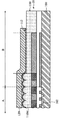
図1Aを参照すると、ダミーパターンを有さない撮像装置10、および、撮像装置10に取り付けられるテープ120の部分断面が示される。撮像装置10は、アクティブ領域Aと周辺領域Bを有する。複数のフォトダイオード102が、アクティブ領域Aで、基板100上に形成される。このほか、マイクロレンズ素子110Mから構成されるマイクロレンズ構造は、アクティブ領域A内のフォトダイオード102上に設置される。マイクロレンズ構造は、マイクロレンズ材料層110で形成される。マイクロレンズ材料層110は、周辺領域Bの一部に延伸する。
Referring to FIG. 1A, a partial cross section of an
さらに、パッシベーション膜112は、周辺領域B内に共形でマイクロレンズ素子110Mとマイクロレンズ材料層110上に形成される。しかし、この実施形態において、周辺領域B中にダミーパターンがない。基板100の薄型化プロセスで、テープ120が撮像装置10に取り付けられるとき、周辺領域B中のマイクロレンズ材料層110上のテープ120とパッシベーション膜112間の接触面積は、周辺領域Bの表面積にほぼ等しい。
Further, the
よって、基板100が薄型化された後、テープ120が撮像装置10から除去されるとき、図1Bに示されるように、元は、周辺領域Bのマイクロレンズ材料層110上に蒸着されていたパッシベーション膜112の一部112Pが剥がされる。パッシベーション膜剥離問題は、不都合なほどに、撮像装置10のパッケージ歩留まりを減少させる。
Therefore, when the
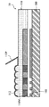
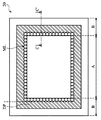
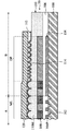
続いて、図2を参照すると、本発明の実施形態によるダミーパターンDPを有する撮像装置20の部分断面が示される。図2において、テープ120が撮像装置20に取り付けられる。撮像装置20は、アクティブ領域Aと周辺領域Bを有する。また、図3は、本発明の複数の実施形態による撮像装置20の平面図である。図3に示されるように、アクティブ領域Aは周辺領域Bにより囲まれる。図2は、図3のC-C’線に沿った撮像装置20の部分断面図である。
Subsequently, referring to FIG. 2, a partial cross-section of the
図2に示されるように、撮像装置20は、複数の光電変換素子102、たとえば、後部研磨プロセスにより薄型化される半導体基板100の正面に形成されるフォトダイオードを含む。半導体基板100は、ウェハか、ウェハから分割されるチップである。光電変換素子102が、アクティブ領域A内に設置される。各光電変換素子102は、撮像装置20の各画素に対応する。さらに、複数の仕切り壁104Pが半導体基板100の正面に設置されて、光電変換素子102を互いに分離する。各仕切り壁104Pは、アクティブ領域A内の二つの隣接する光電変換素子102間に設置される。撮像装置20の各画素は、仕切り壁104Pにより規定される。仕切り壁104Pは、仕切り壁材料層104、たとえば、金属層から形成される。仕切り壁104Pは、蒸着、フォトリソグラフィとエッチングプロセスにより形成される。仕切り壁材料層104は、さらに、周辺領域B内の半導体基板100上に形成される部分104Eを有する。
As shown in FIG. 2, the
撮像装置20の各種配線と電子回路(図示しない)が半導体基板100上に形成される。平坦化層106が半導体基板100上に形成されて、光電変換素子102と仕切り壁材料層104を被覆する。平坦化層106の材料は、有機、または、無機絶縁材料、たとえば、エポキシ樹脂や酸化ケイ素である。
Various wirings and electronic circuits (not shown) of the
カラーフィルター層108が平坦化層106上に形成される。アクティブ領域Aにおいて、平坦化層106は、カラーフィルター層108と光電変換素子102間に設置される。カラーフィルター層108は、複数のカラーフィルター部分、たとえば、それぞれ、赤色、緑色、青色であるカラーフィルター部分108R、108Gおよび108Bを有する。別の実施形態において、カラーフィルター部分は別の配置で配列される別の色を有する。アクティブ領域Aにおいて、各カラーフィルター部分108R,108Gまたは108Bは、撮像装置20の各画素中、個々に、ひとつの光電変換素子102に対応する。さらに、いくつかのカラーフィルター部分は、周辺領域B内、および、仕切り壁材料層104の部分104E上に設置される。カラーフィルター層108は、さらに、周辺領域Bの一部中に設置される延長部分を有する。延長部分108Eは、カラーフィルター部分108R、108Gおよび108Bの一つのカラーを有する。
A
図2と図3を参照すると、マイクロレンズ構造MLが、カラーフィルター層108上に形成される。マイクロレンズ構造MLがアクティブ領域A内に設置され、さらに、周辺領域Bの一部に延伸する。マイクロレンズ構造MLは、アレイ形式で配列された複数のマイクロレンズ素子110Mを有する。マイクロレンズ構造MLは、カラーフィルター層108のカラーフィルター部分と揃えられる。よって、各マイクロレンズ素子110Mは、個々に、カラーフィルター部分に対応する。カラーフィルター層108は、マイクロレンズ構造MLと光電変換素子102間に設置される。さらに、各光電変換素子102は、個々に、一つのカラーフィルター部分に対応すると共に、さらに、一つのマイクロレンズ素子110Mに対応する。
Referring to FIGS. 2 and 3, the microlens structure ML is formed on the
本発明の複数の実施形態によると、ダミーパターンDPは、周辺領域Bの一部中、且つ、マイクロレンズ構造MLに隣接して設置される。図3に示されるように、ダミーパターンDPはマイクロレンズ構造MLを囲む。図2に示されるように、ダミーパターンDPが、カラーフィルター層108の延長部分108E上に形成される。さらに、ダミーパターンDPはマイクロレンズ構造MLと接続する。ダミーパターンDPは、複数の突起素子114を有する。一実施形態において、図2に示されるように、各突起素子114は、各マイクロレンズ素子110Mと同じ形状、たとえば、凸形状を有する。
According to the embodiments of the present invention, the dummy pattern DP is installed in a part of the peripheral region B and adjacent to the microlens structure ML. As shown in FIG. 3, the dummy pattern DP surrounds the microlens structure ML. As shown in FIG. 2, the dummy pattern DP is formed on the
複数の実施形態において、ダミーパターンDPは、マイクロレンズ構造MLと同じ高さである。つまり、凸状の突起素子114の上部は、マイクロレンズ素子110Mの上部と同じ高さである。別の実施形態において、ダミーパターンDPは、マイクロレンズ構造MLより低いか、または、高い。複数の実施形態において、マイクロレンズ構造MLとダミーパターンDPは、同じ材料、たとえば、マイクロレンズ材料層110で形成される。複数の実施形態において、マイクロレンズ構造MLとダミーパターンDPは、同じステップで共に形成される。マイクロレンズ材料ML層110をコートすると共に、マイクロレンズ材料層110上で、フォトリソグラフィとエッチングプロセスを実行することにより、マイクロレンズ構造MLとダミーパターンDPを形成する。
In some embodiments, the dummy pattern DP is the same height as the microlens structure ML. That is, the upper part of the convex projecting
パッシベーション膜112は、共形で、マイクロレンズ構造MLとダミーパターンDPの表面上に形成される。複数の実施形態において、パッシベーション膜112は、連続して、マイクロレンズ構造MLとダミーパターンDPを被覆する。複数の実施形態において、パッシベーション膜112は、化学気相堆積(CVD)により、酸化ケイ素で形成される。図2に示されるように、テープ120が撮像装置20に取り付けられて、半導体基板100の後部研磨プロセス間で撮像装置20を保護する。テープ120は、マイクロレンズ構造MLとダミーパターンDPを被覆し、パッシベーション膜112と接触する。本発明の実施形態によると、ダミーパターンDPは、複数の突起素子114を有する。よって、マイクロレンズ構造MLの外側の周辺領域Bに位置するテープ120は、ダミーパターンDP上部のパッシベーション膜112の一部と接触する。つまり、テープ120は、突起素子114の上部に位置するパッシベーション膜112と接触する。
The
図2の撮像装置20と図1Aの撮像装置10を比較すると、マイクロレンズ構造MLの外側の周辺領域Bにおいて、テープ120とダミーパターンDPを有する撮像装置20のパッシベーション膜112との接触面積は、ダミーパターンDPがない撮像装置10より小さい。つまり、ダミーパターンDPの突起素子114の上部のパッシベーション膜112の表面積は、マイクロレンズ構造MLの外側の周辺領域Bの表面積より小さい。複数の実施形態において、ダミーパターンDP上部、つまり、突起素子114の上部のパッシベーション膜112の表面積は、マイクロレンズ構造MLの外側の周辺領域Bの表面積の約50-80%である。
When the
本発明のダミーパターンDPは、テープ120とパッシベーション膜112間の接触面積を減少させる。さらに、本発明のダミーパターンDPは、パッシベーション膜112とマイクロレンズ材料層110間の接触面積を増加させる。よって、本発明のダミーパターンDPは、テープ120が撮像装置20から除去された後、パッシベーション膜112が剥離するのを効果的に防止する。
The dummy pattern DP of the present invention reduces the contact area between the
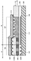
図4は、本発明の実施形態によるダミーパターンDPを有する撮像装置20、および、テープ120が撮像装置20に取り付けられた部分断面図である。図4の撮像装置20のダミーパターンDPは複数の突起素子114を有する。複数の実施形態において、図4の各突起素子は、円錐または角錐状である。一実施形態において、各突起素子114は、同じ円錐形状を有する。円錐形の突起素子114は、とがった先端と円形底部を有する。別の実施形態において、各突起素子114は、同じ角錐形を有する。角錐形の突起素子114は、とがった先端と多角形底面、たとえば、三角形、四角形、五角形、六角形底部を有する。
FIG. 4 is a partial cross-sectional view of the
円錐形、および、角錐形の突起素子114は、パッシベーション膜112とテープ120間の接触面積を減少させる。円錐形と角錐形の突起素子114は、さらに、パッシベーション膜112と、マイクロレンズ構造MLとダミーパターンDPを有するマイクロレンズ材料層110との間の接触面積を増加させる。よって、円錐形または角錐形の突起素子114を有するダミーパターンDPは、テープ120が撮像装置20から除去された後、パッシベーション膜112が剥離するのを効果的に防止する。
The conical and pyramidal
図4に示されるように、複数の実施形態において、ダミーパターンDPは、マイクロレンズ構造MLより低い。別の実施形態において、ダミーパターンDPは、マイクロレンズ構造MLと同じ高さである。つまり、円錐形または角錐形の突起素子114の上部は、マイクロレンズ素子110Mの上部と同じ高さか、または、それより低い。図4の実施形態において、突起素子114の上面は、マイクロレンズ素子110Mの上面より低い。テープ120が撮像装置20に取り付けられるとき、テープ120は、まず、マイクロレンズ素子110Mと接触する。テープ120と突起素子114間の密着性は、テープ120とマイクロレンズ素子110M間より悪い。このほか、テープ120と突起素子114間の接触面は、突起素子114の円錐または角錐状の上部だけにある。よって、突起素子114上に形成されるパッシベーション膜112は、テープ120の影響を受けない。その結果、テープ120が撮像装置20から剥がされるとき、パッシベーション膜112が剥離するのを回避することができる。
As shown in FIG. 4, in some embodiments, the dummy pattern DP is lower than the microlens structure ML. In another embodiment, the dummy pattern DP is the same height as the microlens structure ML. That is, the upper part of the conical or pyramidal
さらに、ダミーパターンDPの円錐形、または、角錐形の突起素子114が、マイクロレンズ構造MLに近い領域で密に配列され、マイクロレンズ構造MLから遠い領域で、まばらに配列されている。ダミーパターンDPのこの配置は、パッシベーション膜112が、マイクロレンズ構造MLから遠い領域で剥離するのを効果的に防止することができる。
Further, the conical or
ダミーパターンDPの円錐形、または、角錐形の突起素子114とマイクロレンズ構造MLは、同じ材料、たとえば、マイクロレンズ材料層110で形成される。複数の実施形態において、ダミーパターンDPの円錐形、または、角錐形の突起素子114は、マイクロレンズ構造MLと別のステップで製造される。たとえば、マイクロレンズ材料層110上で、フォトリソグラフィとエッチングプロセスを実行して、マイクロレンズ素子110Mの形状を形成することにより、マイクロレンズ構造MLが形成される。次に、フォトリソグラフィとエッチングプロセスが、同じマイクロレンズ材料層110で実行されて、ダミーパターンDPの円錐形、または、角錐形の突起素子114の形状を形成する。マイクロレンズ構造MLとダミーパターンDP間の異なる形状は、このプロセスで、異なるフォトマスク、異なる露光条件、または、異なるエッチングレートを用いて得られる。
The conical or
図5は、本発明の実施形態によるダミーパターンDPを有する撮像装置20、および、テープ120が撮像装置20に取り付けられた部分断面図である。図5のダミーパターンDPは複数の突起素子114を有する。複数の実施形態において、各突起素子114は、円柱形または角柱形である。さらに、円柱形、または、角柱形の突起素子114は互いに分離される。一実施形態において、各突起素子114は円柱形を有する。円柱形の突起素子114は、円形上部と円形底部を有する。別の実施形態において、各突起素子114は角柱状の形状を有する。角柱形の突起素子114は、多角形上部と多角形底部、たとえば、三角形上部と三角形底部、四角形上部と四角形底部、五角形上部と五角形底部、または、六角形上部と六角形底部を有する。
FIG. 5 is a partial sectional view of the
パッシベーション膜112は、共形で、円柱形、または、角柱形の突起素子114上に形成される。複数の実施形態において、パッシベーション膜112は、共形で、突起素子114間のマイクロレンズ材料層110の表面に形成される。別の実施形態において、突起素子114間のマイクロレンズ材料層110が除去される。パッシベーション膜112は、共形で、突起素子114間のカラーフィルター層の延長部分108E表面に形成される。
The
周辺領域B内のパッシベーション膜112とテープ120間の接触面積が、分離した円柱形と角柱形の突起素子114により減少する。さらに、周辺領域B内のパッシベーション膜112とマイクロレンズ材料層110間の接触面積は、円柱形のと角柱形の突起素子114により増加する。よって、分離した円柱形と角柱形の突起素子114を有するダミーパターンDPは、テープ120が撮像装置20から除去された後、パッシベーション膜112が剥離するのを効果的に防止する。
The contact area between the
図5に示されるように、複数の実施形態において、ダミーパターンDPは、マイクロレンズ構造MLより低い。別の実施形態において、円柱形、または、角柱形の突起素子114の上部は、マイクロレンズ素子110Mの上部と同じ高さ、または、それより高い。図4の例と比較すると、図5の実施形態において、突起素子114の上面は、マイクロレンズ素子110M上面よりずっと低い。突起素子114の上面は、マイクロレンズ素子110Mの半円形部分の底面より低いか、または、同じ高さである。テープ120が撮像装置20に取り付けられるとき、テープ120は、まず、マイクロレンズ素子110Mと接触する。図4の実施形態と比較すると、図5のテープ120と突起素子114間の密着性は、テープ120とマイクロレンズ素子110M間よりかなり悪い。よって、図5の円柱形、または、角柱形の突起素子114が、図5の突起素子114の先端の形状が図4と異なっていても、図4と同じ効果を達成することができる。共形で、図5の円柱形、または、角柱形の突起素子114上に形成されるパッシベーション膜112も、テープ120より影響されない。その結果、テープ120が図5の撮像装置20から剥がされるとき、パッシベーション膜112が剥離するのを回避することができる。
As shown in FIG. 5, in some embodiments, the dummy pattern DP is lower than the microlens structure ML. In another embodiment, the top of the cylindrical or prismatic
さらに、複数の実施形態において、二つの隣接する円柱形、または、角柱形の突起素子114間の空間は、同じであるかまたは互いに異なる。一実施形態において、マイクロレンズ構造MLの近くの領域内の二つの隣接する突起素子114間の空間は、マイクロレンズ構造MLから遠い領域内の二つの隣接する突起素子114間の空間より小さい。ダミーパターンDPの配置は、パッシベーション膜112が、マイクロレンズ構造MLから遠い領域で剥離するのをさらに効果的に防止する。
Furthermore, in embodiments, the space between two adjacent cylindrical or prismatic
ダミーパターンDPとマイクロレンズ構造MLの円柱形、または、角柱形の突起素子114は、同じ材料、たとえば、マイクロレンズ材料層110で形成される。実施形態において、ダミーパターンDPのマイクロレンズ構造MLと円柱形、または、角柱形の突起素子114は、工程段階で、別々に形成される。マイクロレンズ材料層110上で、フォトリソグラフィとエッチングプロセスを実行して、マイクロレンズ素子110Mを形成することにより、マイクロレンズ構造MLがまず形成される。その後、別のフォトリソグラフィとエッチングプロセスを、同じマイクロレンズ材料層110で実行して、ダミーパターンDPの円柱形、または、角柱形の突起素子114を形成する。マイクロレンズ構造MLとダミーパターンDP間の異なる形状は、工程段階で、異なるフォトマスク、異なる露光条件、異なるエッチングレート等を用いることにより得られる。
The dummy pattern DP and the columnar or prismatic
複数の実施形態において、ダミーパターンDPの突起素子114、たとえば、凸状、円錐形、角錐形、円柱形、または、角柱形の突起素子114は、周辺領域B内に規則的に設置される。一実施形態において、周辺領域Bは、ダミーパターンDPの規則的に設置された突起素子114、たとえば、凸状、円錐形または角錐形の突起素子114により完全に占有される。別の実施形態において、周辺領域Bの一部は、ダミーパターンDPの規則的に設置された突起素子114、たとえば、凸状、円錐形、角錐形、円柱形、または、角柱形の突起素子114により占有されない。
In the plurality of embodiments, the protruding
複数の実施形態において、ダミーパターンDPの突起素子114、たとえば、凸状、円錐形、角錐形、円柱形、または、角柱形の突起素子114は、ランダムに、周辺領域Bに設置される。実施形態において、周辺領域Bの一部は、ダミーパターンDPのランダムに設置された突起素子114、たとえば、凸状、円錐形、角錐形、円柱形、または、角柱形の突起素子114により占有されない。
In the plurality of embodiments, the protruding
実施形態において、入射光は、光電変換素子102を有する半導体基板100の正面に照射する。つまり、光電変換素子102は表面照射型イメージセンサー20を構成する。入射光はマイクロレンズ構造MLにより集光され、カラーフィルター部分108R、108Gおよび108Bと平坦化層106を通過し、その後、光電変換素子102に到達する。
In the embodiment, incident light is applied to the front surface of the
本発明の実施形態によると、撮像装置の周辺領域内のダミーパターン設計は、撮像装置に取り付けられるテープとダミーパターン上に共形で形成されるパッシベーション膜間の接触面積を減少させることができる。さらに、ダミーパターン設計は、マイクロレンズ構造とダミーパターンを形成するのに用いられるパッシベーション膜とマイクロレンズ材料層間の接触面積を増加させる。よって、本発明のダミーパターン設計は、テープが撮像装置から除去されるとき、パッシベーション膜が剥離するのを効果的に防止することができる。本発明のダミーパターン設計は、パッシベーション膜剥離問題を克服し、よって、撮像装置の歩留まりが増加する。さらに、ダミーパターンは、マイクロレンズ構造と同じ材料層で形成される。よって、撮像装置の製造コストが減少する。 According to the embodiment of the present invention, the dummy pattern design in the peripheral region of the imaging device can reduce the contact area between the tape attached to the imaging device and the passivation film formed conformally on the dummy pattern. Furthermore, the dummy pattern design increases the contact area between the microlens structure and the passivation film used to form the dummy pattern and the microlens material layer. Thus, the dummy pattern design of the present invention can effectively prevent the passivation film from peeling when the tape is removed from the imaging device. The dummy pattern design of the present invention overcomes the passivation film delamination problem, thus increasing the yield of the imaging device. Furthermore, the dummy pattern is formed of the same material layer as the microlens structure. Therefore, the manufacturing cost of the imaging device is reduced.
本発明では好ましい実施形態を前述の通り開示したが、これらは決して本発明に限定するものではなく、当該技術を熟知する者なら誰でも、本発明の精神と領域を脱しない範囲内で各種の変動や潤色を加えることができ、従って本発明の保護範囲は、特許請求の範囲で指定した内容を基準とする。 Although preferred embodiments of the present invention have been disclosed in the present invention as described above, these are not intended to limit the present invention in any way, and any person who is familiar with the technology can make various modifications within the spirit and scope of the present invention. Variations and moist colors can be added, so the protection scope of the present invention is based on what is specified in the claims.
10、20〜撮像装置
100〜基板
102〜光電変換素子
104〜仕切り壁材料層
104P〜仕切り壁
104E〜仕切り壁材料層の一部分
106〜平坦化層
108〜カラーフィルター層
108R、108G、108B〜カラーフィルター部分
108E〜延長部分
110〜マイクロレンズ材料層
110M〜マイクロレンズ素子
112〜パッシベーション膜
112P〜パッシベーション膜の一部分
114〜突起素子
120〜テープ
ML〜マイクロレンズ構造
DP〜ダミーパターン
A〜アクティブ領域
B〜周辺領域
10, 20 to 20
Claims (8)
前記撮像装置のアクティブ領域内の基板上に形成される複数の光電変換素子と、
前記アクティブ領域と該アクティブ領域を囲む前記撮像装置の周辺領域の一部に延伸した領域の前記基板上に設置される複数のマイクロレンズ素子を有するマイクロレンズ構造と、
前記マイクロレンズ構造の領域を囲む前記周辺領域内の前記基板上に設置される複数の突起素子を有するダミーパターンと、
前記マイクロレンズ構造の前記複数のマイクロレンズ素子と前記ダミーパターンの前記複数の突起素子の表面上に形成される、製造プロセスにおけるテープの取り付け及び除去の対象となるパッシベーション膜と、を有し、
前記ダミーパターンの上部の前記パッシベーション膜の表面積は、前記マイクロレンズ構造の外側の前記周辺領域の表面積より小さいことを特徴とする撮像装置。 An imaging device,
A plurality of photoelectric conversion elements formed on a substrate in an active region of the imaging device;
A microlens structure having a plurality of microlens elements disposed on the substrate in a region extending to a part of a peripheral region of the imaging device surrounding the active region and the active region ;
A dummy pattern having a plurality of protruding elements installed on the substrate in the peripheral region surrounding the region of the microlens structure ;
A passivation film that is formed on the surfaces of the plurality of microlens elements of the microlens structure and the plurality of protruding elements of the dummy pattern , and is a target for attachment and removal of a tape in a manufacturing process ,
The imaging apparatus according to claim 1, wherein a surface area of the passivation film on the dummy pattern is smaller than a surface area of the peripheral region outside the microlens structure.
前記カラーフィルター層と前記光電変換素子間に設置される平坦化層と、を更に有することを特徴とする請求項1に記載の撮像装置。 A color filter layer installed between the microlens structure and the photoelectric conversion element, having an extension portion installed in the peripheral region, and the dummy pattern installed in the extension portion;
The imaging apparatus according to claim 1, further comprising a planarizing layer disposed between the color filter layer and the photoelectric conversion element.
Applications Claiming Priority (2)
| Application Number | Priority Date | Filing Date | Title |
|---|---|---|---|
| US14/466,412 | 2014-08-22 | ||
| US14/466,412 US10249661B2 (en) | 2014-08-22 | 2014-08-22 | Imaging devices with dummy patterns |
Publications (2)
| Publication Number | Publication Date |
|---|---|
| JP2016046508A JP2016046508A (en) | 2016-04-04 |
| JP6324324B2 true JP6324324B2 (en) | 2018-05-16 |
Family
ID=55348953
Family Applications (1)
| Application Number | Title | Priority Date | Filing Date |
|---|---|---|---|
| JP2015000093A Active JP6324324B2 (en) | 2014-08-22 | 2015-01-05 | Image pickup apparatus having dummy pattern |
Country Status (4)
| Country | Link |
|---|---|
| US (1) | US10249661B2 (en) |
| JP (1) | JP6324324B2 (en) |
| CN (1) | CN105374830B (en) |
| TW (1) | TWI550840B (en) |
Cited By (8)
| Publication number | Priority date | Publication date | Assignee | Title |
|---|---|---|---|---|
| JP3262050B2 (en) | 1997-10-03 | 2002-03-04 | 株式会社村田製作所 | Electronic components and ladder filters |
| JP3262048B2 (en) | 1997-10-01 | 2002-03-04 | 株式会社村田製作所 | Piezoelectric resonator and electronic component using the same |
| JP3262021B2 (en) | 1997-04-25 | 2002-03-04 | 株式会社村田製作所 | Piezoelectric resonator and electronic component using the same |
| JP3262076B2 (en) | 1997-10-03 | 2002-03-04 | 株式会社村田製作所 | Piezoelectric resonator, method for adjusting frequency of piezoelectric resonator, and communication device |
| JP3262077B2 (en) | 1997-10-01 | 2002-03-04 | 株式会社村田製作所 | Electronic components, ladder filters and communication equipment |
| JP3262049B2 (en) | 1997-10-01 | 2002-03-04 | 株式会社村田製作所 | Piezoelectric resonator and electronic component using the same |
| JP3378775B2 (en) | 1997-07-07 | 2003-02-17 | 株式会社村田製作所 | Piezoelectric resonator and frequency adjustment method thereof |
| JP3378163B2 (en) | 1996-08-05 | 2003-02-17 | 株式会社村田製作所 | Piezo components |
Families Citing this family (10)
| Publication number | Priority date | Publication date | Assignee | Title |
|---|---|---|---|---|
| US9927558B2 (en) | 2016-04-19 | 2018-03-27 | Trilumina Corp. | Semiconductor lens optimization of fabrication |
| WO2018043654A1 (en) * | 2016-09-02 | 2018-03-08 | ソニーセミコンダクタソリューションズ株式会社 | Solid-state imaging device and manufacturing method therefor, and electronic apparatus |
| US10170511B1 (en) * | 2017-06-07 | 2019-01-01 | Visera Technologies Company Limited | Solid-state imaging devices having a microlens layer with dummy structures |
| JP7084700B2 (en) * | 2017-06-16 | 2022-06-15 | キヤノン株式会社 | Photoconverter and scanner |
| CN110098218B (en) * | 2018-01-31 | 2024-11-01 | 松下知识产权经营株式会社 | Camera device |
| KR102766214B1 (en) * | 2020-04-06 | 2025-02-12 | 에스케이하이닉스 주식회사 | Image sensing device |
| KR102719043B1 (en) * | 2020-07-10 | 2024-10-22 | 에스케이하이닉스 주식회사 | Image sensing device |
| WO2022130776A1 (en) * | 2020-12-16 | 2022-06-23 | ソニーセミコンダクタソリューションズ株式会社 | Light detection device, light detection system, electronic apparatus, and moving body |
| WO2023151871A1 (en) | 2022-02-10 | 2023-08-17 | Eaton Intelligent Power Limited | Integrated rocker for engine braking with hydraulic lash adjuster |
| JPWO2024048292A1 (en) * | 2022-08-29 | 2024-03-07 |
Family Cites Families (21)
| Publication number | Priority date | Publication date | Assignee | Title |
|---|---|---|---|---|
| JP3291805B2 (en) | 1993-01-26 | 2002-06-17 | ソニー株式会社 | Method for manufacturing solid-state imaging device |
| US6307243B1 (en) * | 1999-07-19 | 2001-10-23 | Micron Technology, Inc. | Microlens array with improved fill factor |
| JP4383959B2 (en) * | 2003-05-28 | 2009-12-16 | キヤノン株式会社 | Photoelectric conversion device and manufacturing method thereof |
| KR100505894B1 (en) | 2003-10-24 | 2005-08-01 | 매그나칩 반도체 유한회사 | Fabricating method of cmos image sensor protecting low temperature oxide delamination |
| US7294818B2 (en) * | 2004-08-24 | 2007-11-13 | Canon Kabushiki Kaisha | Solid state image pickup device and image pickup system comprising it |
| US7919827B2 (en) * | 2005-03-11 | 2011-04-05 | Taiwan Semiconductor Manufacturing Co., Ltd. | Method and structure for reducing noise in CMOS image sensors |
| US7449357B2 (en) * | 2005-04-06 | 2008-11-11 | Magnachip Semiconductor, Ltd. | Method for fabricating image sensor using wafer back grinding |
| JP4944399B2 (en) * | 2005-07-04 | 2012-05-30 | キヤノン株式会社 | Solid-state imaging device |
| JP4876570B2 (en) | 2005-12-22 | 2012-02-15 | 株式会社ニコン | Solid-state imaging device |
| JP2008091399A (en) | 2006-09-29 | 2008-04-17 | Sumitomo Bakelite Co Ltd | Manufacturing method of light receiving device |
| JP4457142B2 (en) | 2007-10-17 | 2010-04-28 | シャープ株式会社 | Solid-state imaging device, camera module, and electronic information device |
| JP5171288B2 (en) | 2008-01-28 | 2013-03-27 | シャープ株式会社 | Solid-state imaging device, mounting method for solid-state imaging device, manufacturing method for solid-state imaging device, and electronic information device |
| JP5357441B2 (en) * | 2008-04-04 | 2013-12-04 | キヤノン株式会社 | Method for manufacturing solid-state imaging device |
| KR101776955B1 (en) * | 2009-02-10 | 2017-09-08 | 소니 주식회사 | Solid-state imaging device, method of manufacturing the same, and electronic apparatus |
| US8039286B2 (en) * | 2009-08-19 | 2011-10-18 | United Microelectronics Corp. | Method for fabricating optical device |
| JP2012064924A (en) * | 2010-08-17 | 2012-03-29 | Canon Inc | Microlens array manufacturing method, solid state image pickup device manufacturing range, and solid state image pickup device |
| JP2012204402A (en) | 2011-03-23 | 2012-10-22 | Toshiba Corp | Solid-state imaging device and method of manufacturing the same |
| JP4872023B1 (en) | 2011-04-22 | 2012-02-08 | パナソニック株式会社 | Solid-state imaging device and manufacturing method thereof |
| JP2012252259A (en) | 2011-06-06 | 2012-12-20 | Seiko Epson Corp | Lens array, image pickup apparatus, biometric authentication apparatus, and electronic apparatus |
| JP5800662B2 (en) * | 2011-10-07 | 2015-10-28 | キヤノン株式会社 | Semiconductor device and manufacturing method thereof |
| JP2014103299A (en) | 2012-11-21 | 2014-06-05 | Toppan Printing Co Ltd | Solid state image sensor |
-
2014
- 2014-08-22 US US14/466,412 patent/US10249661B2/en active Active
- 2014-12-02 TW TW103141731A patent/TWI550840B/en active
- 2014-12-09 CN CN201410748543.1A patent/CN105374830B/en active Active
-
2015
- 2015-01-05 JP JP2015000093A patent/JP6324324B2/en active Active
Cited By (8)
| Publication number | Priority date | Publication date | Assignee | Title |
|---|---|---|---|---|
| JP3378163B2 (en) | 1996-08-05 | 2003-02-17 | 株式会社村田製作所 | Piezo components |
| JP3262021B2 (en) | 1997-04-25 | 2002-03-04 | 株式会社村田製作所 | Piezoelectric resonator and electronic component using the same |
| JP3378775B2 (en) | 1997-07-07 | 2003-02-17 | 株式会社村田製作所 | Piezoelectric resonator and frequency adjustment method thereof |
| JP3262048B2 (en) | 1997-10-01 | 2002-03-04 | 株式会社村田製作所 | Piezoelectric resonator and electronic component using the same |
| JP3262077B2 (en) | 1997-10-01 | 2002-03-04 | 株式会社村田製作所 | Electronic components, ladder filters and communication equipment |
| JP3262049B2 (en) | 1997-10-01 | 2002-03-04 | 株式会社村田製作所 | Piezoelectric resonator and electronic component using the same |
| JP3262050B2 (en) | 1997-10-03 | 2002-03-04 | 株式会社村田製作所 | Electronic components and ladder filters |
| JP3262076B2 (en) | 1997-10-03 | 2002-03-04 | 株式会社村田製作所 | Piezoelectric resonator, method for adjusting frequency of piezoelectric resonator, and communication device |
Also Published As
| Publication number | Publication date |
|---|---|
| JP2016046508A (en) | 2016-04-04 |
| CN105374830A (en) | 2016-03-02 |
| CN105374830B (en) | 2019-03-29 |
| TWI550840B (en) | 2016-09-21 |
| TW201608709A (en) | 2016-03-01 |
| US10249661B2 (en) | 2019-04-02 |
| US20160056187A1 (en) | 2016-02-25 |
Similar Documents
| Publication | Publication Date | Title |
|---|---|---|
| JP6324324B2 (en) | Image pickup apparatus having dummy pattern | |
| US6808960B2 (en) | Method for making and packaging image sensor die using protective coating | |
| JP6763838B2 (en) | Solid-state image sensor with a microlens layer with a dummy structure | |
| JP5630027B2 (en) | Solid-state imaging device, manufacturing method thereof, electronic apparatus, and semiconductor device | |
| CN103579381B (en) | Elevated Photodiode with Crosstalk Isolation | |
| US20160033688A1 (en) | Double-lens structures and fabrication methods thereof | |
| CN207896093U (en) | Imaging sensor and imaging system | |
| US10192916B2 (en) | Methods of fabricating solid-state imaging devices having flat microlenses | |
| JP2009252949A (en) | Solid-state imaging device and manufacturing method thereof | |
| JP2015029011A (en) | Solid-state imaging device, method for manufacturing the same, and electronic apparatus | |
| CN111758165A (en) | Solid-state imaging device and solid-state imaging device | |
| CN103928479B (en) | Solid-state imaging apparatus and manufacture method thereof | |
| JP2011146633A (en) | Method of manufacturing solid-state image sensor | |
| JP5876104B2 (en) | Image sensor and camera module having microlens protection pattern | |
| US20080224245A1 (en) | Image sensor and method for manufacturing the same | |
| CN101266947A (en) | Image sensor and manufacturing method thereof | |
| JP6154862B2 (en) | Image sensor structure | |
| KR20100007512A (en) | Image sensor and method of manufacturing the same | |
| JP2013161873A (en) | Solid-state imaging device and camera module | |
| KR100907158B1 (en) | Image sensor and its manufacturing method | |
| KR100739999B1 (en) | CMOS image sensor and manufacturing method | |
| KR20100079556A (en) | Cmos image sensor and method for manufacturing the same |
Legal Events
| Date | Code | Title | Description |
|---|---|---|---|
| A131 | Notification of reasons for refusal |
Free format text: JAPANESE INTERMEDIATE CODE: A131 Effective date: 20160523 |
|
| A521 | Request for written amendment filed |
Free format text: JAPANESE INTERMEDIATE CODE: A523 Effective date: 20160819 |
|
| A02 | Decision of refusal |
Free format text: JAPANESE INTERMEDIATE CODE: A02 Effective date: 20170206 |
|
| A521 | Request for written amendment filed |
Free format text: JAPANESE INTERMEDIATE CODE: A523 Effective date: 20170411 |
|
| A911 | Transfer to examiner for re-examination before appeal (zenchi) |
Free format text: JAPANESE INTERMEDIATE CODE: A911 Effective date: 20170419 |
|
| A912 | Re-examination (zenchi) completed and case transferred to appeal board |
Free format text: JAPANESE INTERMEDIATE CODE: A912 Effective date: 20170623 |
|
| A521 | Request for written amendment filed |
Free format text: JAPANESE INTERMEDIATE CODE: A523 Effective date: 20171207 |
|
| A61 | First payment of annual fees (during grant procedure) |
Free format text: JAPANESE INTERMEDIATE CODE: A61 Effective date: 20180410 |
|
| R150 | Certificate of patent or registration of utility model |
Ref document number: 6324324 Country of ref document: JP Free format text: JAPANESE INTERMEDIATE CODE: R150 |
|
| R250 | Receipt of annual fees |
Free format text: JAPANESE INTERMEDIATE CODE: R250 |
|
| R250 | Receipt of annual fees |
Free format text: JAPANESE INTERMEDIATE CODE: R250 |
|
| R250 | Receipt of annual fees |
Free format text: JAPANESE INTERMEDIATE CODE: R250 |