JP6316578B2 - Scanning electron microscope system, pattern measuring method using the same, and scanning electron microscope - Google Patents
Scanning electron microscope system, pattern measuring method using the same, and scanning electron microscope Download PDFInfo
- Publication number
- JP6316578B2 JP6316578B2 JP2013249249A JP2013249249A JP6316578B2 JP 6316578 B2 JP6316578 B2 JP 6316578B2 JP 2013249249 A JP2013249249 A JP 2013249249A JP 2013249249 A JP2013249249 A JP 2013249249A JP 6316578 B2 JP6316578 B2 JP 6316578B2
- Authority
- JP
- Japan
- Prior art keywords
- pattern
- electron beam
- hole
- backscattered
- electron microscope
- Prior art date
- Legal status (The legal status is an assumption and is not a legal conclusion. Google has not performed a legal analysis and makes no representation as to the accuracy of the status listed.)
- Active
Links
Images


Classifications
-
- H—ELECTRICITY
- H01—ELECTRIC ELEMENTS
- H01J—ELECTRIC DISCHARGE TUBES OR DISCHARGE LAMPS
- H01J37/00—Discharge tubes with provision for introducing objects or material to be exposed to the discharge, e.g. for the purpose of examination or processing thereof
- H01J37/02—Details
- H01J37/244—Detectors; Associated components or circuits therefor
-
- H—ELECTRICITY
- H01—ELECTRIC ELEMENTS
- H01J—ELECTRIC DISCHARGE TUBES OR DISCHARGE LAMPS
- H01J37/00—Discharge tubes with provision for introducing objects or material to be exposed to the discharge, e.g. for the purpose of examination or processing thereof
- H01J37/26—Electron or ion microscopes; Electron or ion diffraction tubes
- H01J37/29—Reflection microscopes
-
- G—PHYSICS
- G01—MEASURING; TESTING
- G01B—MEASURING LENGTH, THICKNESS OR SIMILAR LINEAR DIMENSIONS; MEASURING ANGLES; MEASURING AREAS; MEASURING IRREGULARITIES OF SURFACES OR CONTOURS
- G01B15/00—Measuring arrangements characterised by the use of electromagnetic waves or particle radiation, e.g. by the use of microwaves, X-rays, gamma rays or electrons
- G01B15/04—Measuring arrangements characterised by the use of electromagnetic waves or particle radiation, e.g. by the use of microwaves, X-rays, gamma rays or electrons for measuring contours or curvatures
-
- H—ELECTRICITY
- H01—ELECTRIC ELEMENTS
- H01J—ELECTRIC DISCHARGE TUBES OR DISCHARGE LAMPS
- H01J37/00—Discharge tubes with provision for introducing objects or material to be exposed to the discharge, e.g. for the purpose of examination or processing thereof
- H01J37/26—Electron or ion microscopes; Electron or ion diffraction tubes
- H01J37/28—Electron or ion microscopes; Electron or ion diffraction tubes with scanning beams
-
- G—PHYSICS
- G01—MEASURING; TESTING
- G01B—MEASURING LENGTH, THICKNESS OR SIMILAR LINEAR DIMENSIONS; MEASURING ANGLES; MEASURING AREAS; MEASURING IRREGULARITIES OF SURFACES OR CONTOURS
- G01B2210/00—Aspects not specifically covered by any group under G01B, e.g. of wheel alignment, caliper-like sensors
- G01B2210/56—Measuring geometric parameters of semiconductor structures, e.g. profile, critical dimensions or trench depth
-
- H—ELECTRICITY
- H01—ELECTRIC ELEMENTS
- H01J—ELECTRIC DISCHARGE TUBES OR DISCHARGE LAMPS
- H01J2237/00—Discharge tubes exposing object to beam, e.g. for analysis treatment, etching, imaging
- H01J2237/244—Detection characterized by the detecting means
- H01J2237/24475—Scattered electron detectors
-
- H—ELECTRICITY
- H01—ELECTRIC ELEMENTS
- H01J—ELECTRIC DISCHARGE TUBES OR DISCHARGE LAMPS
- H01J2237/00—Discharge tubes exposing object to beam, e.g. for analysis treatment, etching, imaging
- H01J2237/244—Detection characterized by the detecting means
- H01J2237/2448—Secondary particle detectors
-
- H—ELECTRICITY
- H01—ELECTRIC ELEMENTS
- H01J—ELECTRIC DISCHARGE TUBES OR DISCHARGE LAMPS
- H01J2237/00—Discharge tubes exposing object to beam, e.g. for analysis treatment, etching, imaging
- H01J2237/244—Detection characterized by the detecting means
- H01J2237/24495—Signal processing, e.g. mixing of two or more signals
-
- H—ELECTRICITY
- H01—ELECTRIC ELEMENTS
- H01J—ELECTRIC DISCHARGE TUBES OR DISCHARGE LAMPS
- H01J2237/00—Discharge tubes exposing object to beam, e.g. for analysis treatment, etching, imaging
- H01J2237/26—Electron or ion microscopes
- H01J2237/28—Scanning microscopes
- H01J2237/2803—Scanning microscopes characterised by the imaging method
- H01J2237/2806—Secondary charged particle
-
- H—ELECTRICITY
- H01—ELECTRIC ELEMENTS
- H01J—ELECTRIC DISCHARGE TUBES OR DISCHARGE LAMPS
- H01J2237/00—Discharge tubes exposing object to beam, e.g. for analysis treatment, etching, imaging
- H01J2237/26—Electron or ion microscopes
- H01J2237/28—Scanning microscopes
- H01J2237/2809—Scanning microscopes characterised by the imaging problems involved
- H01J2237/281—Bottom of trenches or holes
-
- H—ELECTRICITY
- H01—ELECTRIC ELEMENTS
- H01J—ELECTRIC DISCHARGE TUBES OR DISCHARGE LAMPS
- H01J2237/00—Discharge tubes exposing object to beam, e.g. for analysis treatment, etching, imaging
- H01J2237/26—Electron or ion microscopes
- H01J2237/28—Scanning microscopes
- H01J2237/2813—Scanning microscopes characterised by the application
- H01J2237/2814—Measurement of surface topography
- H01J2237/2815—Depth profile
-
- H—ELECTRICITY
- H01—ELECTRIC ELEMENTS
- H01L—SEMICONDUCTOR DEVICES NOT COVERED BY CLASS H10
- H01L22/00—Testing or measuring during manufacture or treatment; Reliability measurements, i.e. testing of parts without further processing to modify the parts as such; Structural arrangements therefor
- H01L22/10—Measuring as part of the manufacturing process
- H01L22/12—Measuring as part of the manufacturing process for structural parameters, e.g. thickness, line width, refractive index, temperature, warp, bond strength, defects, optical inspection, electrical measurement of structural dimensions, metallurgic measurement of diffusions
Description
本発明は、半導体ウェハ上に形成されたパターンの寸法計測を行う方法に係り、特にアスペクト比が高い穴パターンや溝パターンの寸法測定を行う走査電子顕微鏡システム及びそれを用いたパターン計測方法並びに走査電子顕微鏡に関する。 The present invention relates to a method for measuring dimensions of a pattern formed on a semiconductor wafer, and more particularly, to a scanning electron microscope system for measuring dimensions of a hole pattern or a groove pattern having a high aspect ratio, a pattern measuring method using the same, and a scanning method. It relates to an electron microscope.
半導体製造工程でのパターン寸法管理には、走査電子顕微鏡(Scanning Electron Microscope:SEM)を半導体専用に特化した測長SEMが広く用いられている。図2Aに従来の測長SEMの基本構成を示す。電子銃101から放出された、一次電子ビーム102はコンデンサレンズ103で細く絞られ、偏向器104により試料上を2次元的に走査される。加速電圧としては、1kV程度の比較的低加速電圧が用いられることが一般的である。電子ビーム照射によって試料107から発生した二次電子120を検出器121で捕らえることで二次電子線像が得られる。傾斜角効果、あるいは、エッジ効果によって、二次電子線像上ではパターンエッジ部が明るい画像となるので、画像処理手法によりエッジ位置を検出することによって寸法が求められる。
For pattern dimension management in a semiconductor manufacturing process, a scanning electron microscope (SEM) that is specialized for a semiconductor is used widely. FIG. 2A shows a basic configuration of a conventional length measuring SEM. The
半導体デバイスのコスト低減は、微細化によってチップ面積を小さくすることによって実現されてきたが、チップ面積を小さくすることによって得られるコストメリットをリソグラフィなどの製造コストの増加が相殺するようになってきた。NANDフラッシュメモリにおいては、新たなコスト低減策として、メモリセルアレイを積み上げて3次元化する技術(3D−NAND)の開発が加速している。 The cost reduction of semiconductor devices has been realized by reducing the chip area by miniaturization, but the cost merit obtained by reducing the chip area has been offset by the increase in manufacturing costs such as lithography. . In the NAND flash memory, as a new cost reduction measure, development of a technology (3D-NAND) for stacking memory cell arrays into a three-dimensional structure is accelerating.
3D−NANDは、電極膜と絶縁膜を交互に積層した後に、最上層から最下層に貫通する穴を一度に開け(図3A参照)、穴側面にメモリ膜を形成し、柱状電極を埋め込むという工程を経て形成される。同プロセスの成否を握っているのは穴開け工程であり、適正な径の穴が、最下層まで貫通することがキーとなる。穴の開口/非開口、あるいは、穴のトップ径/ボトム径の管理が求められている。 In 3D-NAND, after alternately laminating electrode films and insulating films, a hole penetrating from the uppermost layer to the lowermost layer is formed at once (see FIG. 3A), a memory film is formed on the side surface of the hole, and a columnar electrode is embedded. It is formed through a process. The success or failure of this process is the drilling process, and the key is that a hole with an appropriate diameter penetrates to the lowest layer. There is a need to manage the opening / non-opening of holes or the top / bottom diameter of holes.
穴の開口/非開口、あるいは、穴のトップ径/ボトム径を観察する技術として、例えば特許文献1には、試料の溝又は孔の側壁或いは低面で反射した電子が、試料内を貫通して試料表面から脱出或いは試料表面で三次電子を発生させるに足る十分なエネルギを持つような高エネルギの一次電子を試料に照射してアスペクト比が3前後の穴パターンを観察する走査型電子顕微鏡について記載されている。特許文献1では、一次電子の加速電圧として、100kV及び200kVの例を示している。
As a technique for observing the opening / non-opening of a hole or the top diameter / bottom diameter of a hole, for example,
また、特許文献1には、反射電子を対物レンズと思量との間に配置してシンチレータで検出し、対物レンズの中心の空洞部分を通過した三次電子を引き出し電界で引き出してシンチレータで検出する構成が記載されている。
一方、特許文献2には、走査型電子顕微鏡を用いて50kV以上で加速した電子線を試料に照射して、試料から発生した2次電子や3次電子をシンチレータで検出して、孔や溝内部を観察することが記載されている。また、特許文献1と同様に、反射電子を対物レンズと試料との間に配置してシンチレータで検出し、対物レンズの中心の空洞部分を通過した三次電子を引き出し電界で引き出してシンチレータで検出する構成が記載されている。
On the other hand, in
上記穴開け工程を管理するためには、穴径約50nm、深さ2um以上という非常に高アスペクト比の穴の検査・計測を行う必要がある。しかしながら、図2Bに示すように、従来の測長SEMにおいては、穴内部で発生した二次電子は、外に脱出する前に内壁に衝突して消滅するため、穴底からの信号はほとんど得られず、特に重要な穴のボトム径を計測できないという課題があった。 In order to manage the drilling process, it is necessary to inspect and measure a very high aspect ratio hole having a hole diameter of about 50 nm and a depth of 2 μm or more. However, as shown in FIG. 2B, in the conventional length measurement SEM, secondary electrons generated inside the hole collide with the inner wall before escaping to the outside and disappear, so that almost no signal is obtained from the hole bottom. In particular, there was a problem that the bottom diameter of particularly important holes could not be measured.
特許文献1に記載されている方法によれば、穴の底から発生した高エネルギーの反射電子と、この高エネルギーの反射電子が孔の側壁を透過することにより発生する三次電子とを吸引電極で分離して、それぞれ検出する構成が記載されている。しかし、アスペクト比が大きい細くて深い穴が形成された試料から発生する三次信号のレベルは一般的に低くなる。従って、特許文献1に記載されているような三次電子を吸引電極で吸引して検出する構成では、試料から発生した三次電子のうち一部しか検出することができず、アスペクト比が大きい細くて深い穴を観察する場合に、十分な三次電子の検出信号レベルを確保することが難しい。
According to the method described in
また、特許文献1に記載されている、反射電子を対物レンズと試料との間に配置したシンチレータで検出し、対物レンズの中心の空洞部分を通過した三次電子を引き出し電界で引き出してシンチレータで検出する構成では、試料から発生した三次電子のうち対物レンズの中心の空洞部分を通過した一部の三次電子しか検出することができず、十分な三次電子の検出信号レベルを確保することが難しい。更に、アスペクト比が大きい深い穴の底から発生した反射電子のうち孔の開口部から外部に放出される反射電子は、孔の中心軸に沿った方向に進む成分が多くなるために、対物レンズの中心の空洞部分を除いてその周りに配置したシンチレータでは検出することが難しくなる。一方、特許文献2に記載されている走査型電子顕微鏡装置においても、開示されているシンチレータでは、試料から発生した三次電子のうち一部しか検出することができず、十分な三次電子の検出信号レベルを確保することが難しいことに加えて、アスペクト比が大きい深い穴の底から発生した反射電子は、孔の中心軸に沿った方向に進む成分が多くなるために、対物レンズの中心の空洞部分を除いてその周りに配置したシンチレータでは検出することが難しくなる。
Moreover, the reflected electrons described in
本発明は、上記した従来技術の課題を解決して、高アスペクト比の穴径又は溝幅の計測を可能にするとともに、穴又は溝の深さの計測を可能にする走査電子顕微鏡システム及びそれを用いたパターン計測方法並びに走査電子顕微鏡を提供するものである。 The present invention solves the above-mentioned problems of the prior art, enables measurement of a hole diameter or groove width with a high aspect ratio, and enables measurement of a hole or groove depth and a scanning electron microscope system thereof And a scanning electron microscope.
上記した課題を解決するために、本発明では、基板上に形成された穴パターン又は溝パターンを計測する走査電子顕微鏡システムを、基板上に形成されたパターンに対して一次電子線を走査して照射する一次電子線照射手段と、一次電子線照射手段により一次電子線が照射された基板から放出される後方散乱電子のうち穴パターン又は溝パターンの側壁を突き抜けた後方散乱電子を検出する後方散乱電子検出手段と、後方散乱電子検出手段で検出した後方散乱電子の強度分布に対応する電子線像を生成する電子線像生成手段と、電子線像生成手段で生成した電子線像上の明部領域内に存在する暗部領域の明部領域との境界領域を求めて、この求めた境界領域を穴パターン又は溝パターンのエッジ位置として検出する画像処理手段とを備えて構成した。 In order to solve the above-described problems, in the present invention, a scanning electron microscope system that measures a hole pattern or a groove pattern formed on a substrate is scanned with a primary electron beam with respect to the pattern formed on the substrate. Backscattering for detecting backscattered electrons penetrating through the side wall of the hole pattern or groove pattern among the irradiated primary electron beam irradiation means and the backscattered electrons emitted from the substrate irradiated with the primary electron beam by the primary electron beam irradiation means Electron detection means, electron beam image generation means for generating an electron beam image corresponding to the intensity distribution of backscattered electrons detected by the backscattered electron detection means, and a bright portion on the electron beam image generated by the electron beam image generation means Image processing means for obtaining a boundary area between the dark area and the bright area existing in the area and detecting the obtained boundary area as an edge position of a hole pattern or a groove pattern. It was.
また、上記した課題を解決するために、本発明では、基板上に形成された穴パターン又は溝パターンを計測する走査電子顕微鏡システムを、基板上に形成されたパターンに対して一次電子線を走査して照射する一次電子線照射手段と、一次電子線照射手段により一次電子線が照射された基板から放出される後方散乱電子のうち穴パターン又は溝パターンの側壁を突き抜けた後方散乱電子を検出する後方散乱電子検出手段と、後方散乱電子検出手段で検出した後方散乱電子の強度分布に対応する電子線像を生成する電子線像生成手段と、電子線像生成手段で生成した電子線像上の明部領域内に存在する暗部領域の明部領域との境界領域を求めて、この求めた境界領域の内部の暗部領域の明るさの情報から穴パターン又は溝パターンの深さを推定する深さ推定手段とを備えて構成した。 In order to solve the above-described problems, in the present invention, a scanning electron microscope system that measures a hole pattern or a groove pattern formed on a substrate is scanned with a primary electron beam with respect to the pattern formed on the substrate. And detecting backscattered electrons penetrating through the side wall of the hole pattern or groove pattern among the backscattered electrons emitted from the substrate irradiated with the primary electron beam by the primary electron beam irradiating means. Backscattered electron detection means, electron beam image generation means for generating an electron beam image corresponding to the intensity distribution of backscattered electrons detected by the backscattered electron detection means, and on the electron beam image generated by the electron beam image generation means The boundary area between the dark area and the bright area in the bright area is obtained, and the depth of the hole pattern or groove pattern is estimated from the brightness information of the dark area inside the obtained boundary area. Was constructed and a depth estimation unit that.
また、上記した課題を解決するために、本発明では、基板上に形成された穴パターン又は溝パターンを計測する走査電子顕微鏡システムを、基板上に形成されたパターンに対して一次電子線を走査して照射する一次電子線照射手段と、一次電子線照射手段により一次電子線が照射された基板から放出される後方散乱電子のうち穴パターン又は溝パターンの側壁を突き抜けた後方散乱電子を検出する後方散乱電子検出手段と、後方散乱電子検出手段で検出した後方散乱電子の強度分布に対応する電子線像を生成する電子線像生成手段と、電子線像生成手段で生成した電子線像上の明部領域内に存在する暗部領域の明部領域との境界領域を求めて、この求めた境界領域を穴パターン又は溝パターンのエッジ位置として検出する画像処理手段と、電子線像生成手段で生成した電子線像上の明部領域内に存在する暗部領域の明部領域との境界領域を求めて、この求めた境界領域の内部の暗部領域の明るさの情報から穴パターン又は溝パターンの深さを推定する深さ推定手段とを備えて構成した。 In order to solve the above-described problems, in the present invention, a scanning electron microscope system that measures a hole pattern or a groove pattern formed on a substrate is scanned with a primary electron beam with respect to the pattern formed on the substrate. And detecting backscattered electrons penetrating through the side wall of the hole pattern or groove pattern among the backscattered electrons emitted from the substrate irradiated with the primary electron beam by the primary electron beam irradiating means. Backscattered electron detection means, electron beam image generation means for generating an electron beam image corresponding to the intensity distribution of backscattered electrons detected by the backscattered electron detection means, and on the electron beam image generated by the electron beam image generation means An image processing means for obtaining a boundary area between the dark area and the bright area in the bright area, and detecting the obtained boundary area as an edge position of the hole pattern or groove pattern; The boundary area between the dark area and the bright area existing in the bright area on the electron beam image generated by the line image generation means is obtained, and the hole information is obtained from the brightness information of the dark area inside the obtained boundary area. And a depth estimating means for estimating the depth of the pattern or groove pattern.
更にまた、上記した課題を解決するために、本発明では、基板上に形成された穴パターン又は溝パターンを計測する走査電子顕微鏡システムを用いたパターン計測方法において、電子顕微鏡で基板上に形成された穴パターン又は溝パターンに対して一次電子線を走査して照射し、一次電子線が照射された基板から放出される後方散乱電子のうち穴パターン又は溝パターンの側壁を突き抜けた後方散乱電子を検出し、検出した後方散乱電子の強度分布に対応する電子線像を生成し、この生成した電子線像上の明部領域内に存在する暗部領域の明部領域との境界領域を求め、この求めた境界領域を穴パターン又は溝パターンのエッジ位置として検出することと、求めた境界領域の内部の暗部領域の明るさの情報から穴パターン又は溝パターンの深さを推定することの何れか又は両方を行うようにした。 Furthermore, in order to solve the above-described problems, in the present invention, in a pattern measurement method using a scanning electron microscope system that measures a hole pattern or a groove pattern formed on a substrate, the pattern is formed on the substrate with an electron microscope. Back-scattered electrons penetrating through the sidewalls of the hole pattern or groove pattern among the back-scattered electrons emitted from the substrate irradiated with the primary electron beam are scanned and irradiated to the hole pattern or groove pattern. Detecting, generating an electron beam image corresponding to the detected intensity distribution of the backscattered electrons, obtaining a boundary region between the bright region and the bright region in the bright region on the generated electron beam image, The detected boundary area is detected as the edge position of the hole pattern or groove pattern, and the depth information of the hole pattern or groove pattern is obtained from the brightness information of the dark area inside the determined boundary area. Was to perform either or both of estimating.
更にまた、上記した課題を解決するために、本発明では、基板上に形成された穴パターン又は溝パターンを計測する電子顕微鏡を、基板上に形成されたパターンに対して一次電子線を走査して照射する一次電子線照射手段と、一次電子線照射手段により一次電子線が照射された基板から放出される後方散乱電子のうち穴パターン又は溝パターンの側壁を突き抜けた後方散乱電子を検出する後方散乱電子検出手段と、後方散乱電子検出手段で検出した後方散乱電子の強度分布に対応する電子線像を生成する電子線像生成手段とを備えて構成した。 Furthermore, in order to solve the above-described problems, in the present invention, an electron microscope that measures the hole pattern or groove pattern formed on the substrate is scanned with the primary electron beam with respect to the pattern formed on the substrate. And detecting backscattered electrons penetrating through the side wall of the hole pattern or groove pattern among the backscattered electrons emitted from the substrate irradiated with the primary electron beam by the primary electron beam irradiating means. The apparatus includes a scattered electron detection unit and an electron beam image generation unit that generates an electron beam image corresponding to the intensity distribution of the backscattered electrons detected by the backscattered electron detection unit.
本発明によれば、高アスペクト比の穴径の計測が可能になるとともに、穴深さの計測が可能となる。 According to the present invention, it is possible to measure a hole diameter with a high aspect ratio and to measure a hole depth.
本発明は、試料に高加速電圧の電子線を照射し、低角度(例えば仰角5度以上)の後方散乱電子(BSE)を検出することによって、穴底から放出され側壁を突き抜けた、“突き抜けBSE”で穴底観察を行うようにしたものである。なお、本明細書においては、仰角を、計測対象である試料の表面の法線方向と放出電子の放出方向との成す角度として定義する。 The present invention irradiates a specimen with an electron beam having a high acceleration voltage and detects backscattered electrons (BSE) at a low angle (for example, an elevation angle of 5 degrees or more), thereby ejecting from a hole bottom and penetrating a side wall. The hole bottom is observed with “BSE”. In the present specification, the elevation angle is defined as the angle formed by the normal direction of the surface of the sample to be measured and the emission direction of the emitted electrons.
また、穴が深いと突き抜け距離が相対的に長くなるので、突き抜けBSEの量が減って像が暗くなるという特性を利用して、穴深さと明るさの関係を表す検量線を与えて、穴深さの計測を行うようにした。
以下、実施例を図面を用いて説明する。
Further, since the penetration distance becomes relatively long when the hole is deep, a calibration curve representing the relationship between the hole depth and the brightness is given using the characteristic that the amount of the penetration BSE is reduced and the image becomes dark. The depth was measured.
Hereinafter, examples will be described with reference to the drawings.
図1Aは本発明が適用される走査電子顕微鏡システム100の基本構成である。電子顕微鏡システム100は、撮像光学系001、制御部021、演算部022、記憶部023、および入出力部024等から構成される。撮像光学系001は、電子銃101から高加速電圧(例えば30kV以上)の1次電子ビーム102を発生し、この1次電子ビーム102をコンデンサレンズ103で集束し、さらに対物レンズ105に通すことにより試料200の表面に集束する。
FIG. 1A is a basic configuration of a scanning
1次電子ビーム102は、偏向器104により試料200の上を2次元的に走査される。試料200から放出される低角度方向の後方散乱電子110を環状のYAGシンチレータ106(図1B参照)で受けて光信号に変換し、光ファイバ111により高電子増倍管112に導き、画像生成部113によりデジタル画像を生成する。この際、画像が適正な明るさになるよう、明るさ補正が行われるのが一般的である。撮像された画像は、記憶部023に保存される。ステージ108を移動することにより、試料の任意の位置での画像撮像が可能である。
The
制御部021は、電子銃101周辺に印加する電圧、コンデンサレンズ104および対物レンズ105の焦点位置調整、ステージ108の移動、画像生成部113の動作タイミング等を制御する。演算部022では、撮像画像を用いて寸法計測処理を行う。試料情報の入力、撮像条件の入力、寸法計測結果の出力等は、入出力部024により行われる。
The control unit 021 controls the voltage applied to the periphery of the
図1Aに示したような構成を用いて、高エネルギー(高加速電圧)の一次電子線を試料200に照射することにより、試料200からは高エネルギーの後方散乱電子(Back Scattered Electron: BSE)が放出される。この放出されたBSEは、図1Cに示したように、試料200に形成した穴210の側壁を突き抜けて、円環型のシンチレータ106に達する。これにより、穴底の観察が可能となる。
By irradiating the
従来技術の場合も、穴底に一次電子が照射されれば、BSEが放出されるが、一次電子が低エネルギー(低加速電圧)なので、BSEのエネルギーも低く、従って、大半のBSEは側壁内を進むうちにエネルギーを失って、突き抜けられない(図2B参照)。 In the case of the prior art as well, BSE is emitted if primary electrons are irradiated to the bottom of the hole. However, since the primary electrons are low energy (low acceleration voltage), the energy of BSE is also low. The energy is lost while proceeding, and cannot be penetrated (see FIG. 2B).
本発明は、高加速電圧と低角BSE(試料200の表面の法線方向との成す角度が比較的大きい方向に発生したBSE)を組み合わせることで、“突き抜けBSE”という、従来とは異なる検出原理に基づく穴底観察を可能にしたものといえる。
In the present invention, a combination of a high acceleration voltage and a low angle BSE (a BSE generated in a direction in which the angle formed by the normal direction of the surface of the
なお、低角BSEの検出には、YAGシンチレータ106の他、環状の半導体検出器、あるいは、ロビンソン型検出器を用いてもよい。また、環状の代わりに、複数方向に検出器を配置するような構成してもよい。
In addition to detecting the low-angle BSE, an annular semiconductor detector or a Robinson detector may be used in addition to the
本発明の有効性を電子線シミュレーション(モンテカルロシミュレーション)によって確認した結果を図4A乃至図4Dに示す。図4Aの場合、サンプル401に形成された穴411の断面形状は、トップ径td1:70nm、ボトム径bd1:70nm、穴深さhd1:3.2umのホール(以下、t70b70ホールと記す)、また図4Bの場合、サンプル402に形成された穴412の、断面形状は、トップ径td2:70nm、ボトム径bd2:30nm、穴深さhd2:3.2umのホール(以下、t70b30ホールと記す)のを示す。加速電圧は30kVとし、二次電子像(Secondary Electron Image: SE像)は、エネルギーが50eV以下の電子を検出することによって、低角BSE像は、エネルギーが5000eV以上、放出電子の仰角(本明細書においては、仰角を試料200の表面の法線方向と放出電子の放出方向との成す角度として定義する)が15−65度の電子を検出することによって得た。
The results of confirming the effectiveness of the present invention by electron beam simulation (Monte Carlo simulation) are shown in FIGS. 4A to 4D. In the case of FIG. 4A, the cross-sectional shape of the
図4A及び図4Bに示した断面形状が異なる穴411、412が形成されたサンプル401と402に一次電子ビーム102を照射したときに検出されるSE像の信号波形を図4Cに、低角BSE像の信号波形を図4Dに示す。同図の横軸は穴411または412の中心からの距離である。t70b70ホールにおいては、x=35nmが穴底エッジ、t70b30ホールにおいては、x=15nmがボトムエッジ端に相当する。同図の縦軸は検出信号強度(Yield)である。
The signal waveform of the SE image detected when the
SE像の場合、図4Cのように、t70b70ホール(図4Aの穴411)が形成された試料401から検出されたSE像の信号波形421及び、t70b30ホール(図4Bの穴412)が形成された試料402から検出された低角BSE像の信号波形422において、穴底部の信号強度が必要に小さく、この信号波形からボトムエッジ位置を検出するのは困難である。
In the case of the SE image, as shown in FIG. 4C, the
一方、低角BSE像の場合、図4Dのように、t70b70ホール(図4Aの穴411)が形成された試料401から検出された低角BSE像431の信号波形の立ち上がり位置はx=35nm付近に、t70b30ホール(図4Bの穴412)が形成された試料402から検出された低角BSE像432の信号波形の立ち上がり位置はx=15nm付近にあり、SE像よりも、穴底エッジ位置の検出に適していることが分かる。
On the other hand, in the case of the low-angle BSE image, as shown in FIG. 4D, the rising position of the signal waveform of the low-
穴底エッジ位置の具体的な検出方法を図5A乃至図5Cに示す。図5Aのように、ホールパターンの低角BSE像501は、ホール内502が暗く、ホール外503が明るい画像となる。穴側壁が切り立っている場合はエッジがシャープな画像に、穴側壁にテーパがある場合は、エッジがぼけた画像となる。図5B、図5Cの信号波形510および520は、図5Aのホール502を横切るA−Aのスライス波形である。図4Dが示すように、ボトムエッジ端は、信号波形の立ち上がり位置なので、図5Bのように、信号波形のボトム領域と、スロープ領域に対して、それぞれ、Bottom line:511、Slope line:512を当てはめ、これらの交点をボトムエッジ端513として検出し、ボトム径514を求める。あるいは、図5Cのように、信号波形のmax値521とmin値522を適当な比で内分するしきい値を与えて、しきい値と信号波形との交点をエッジ点としても良い。この際、大小二つのしきい値(th1:523とth2:524)を与えて、穴径1:525と穴径2:526を求めるようにしても良い。穴径1:525と穴径2:526の差(穴径1−穴径2)を側壁傾斜角指標値として、この側壁傾斜角指標値の大小によって、側壁テーパの大小をモニタすることが可能である。
A specific method for detecting the hole bottom edge position is shown in FIGS. 5A to 5C. As shown in FIG. 5A, the low-
以上述べた、実施例1は本発明の基本構成である。本実施の形態によれば、従来技術では計測不可能であった、高アスペクト比の穴径計測が可能となる。 The first embodiment described above is the basic configuration of the present invention. According to the present embodiment, it is possible to measure a hole diameter with a high aspect ratio, which is impossible to measure with the prior art.
本実施例では、穴径だけでなく、穴深さの計測を行う方法を提供する。
本発明は、側壁を突き抜けたBSEを検出することで穴底観察を実現しているが、穴が深くアスペクト比が大きくなると、穴の底から放出された電子が側壁を突き抜けて表面に達するのに要する距離が長くなるため、途中でエネルギーを使い果たして突き抜けられなくなる電子の比率が増加する。換言すると、撮像画像上では、穴が深いほど穴部が暗いという関係を用いることで、穴深さを計測(推定)することが可能である。
The present embodiment provides a method for measuring not only the hole diameter but also the hole depth.
The present invention realizes hole bottom observation by detecting BSE that penetrates the side wall, but when the hole is deep and the aspect ratio is large, electrons emitted from the bottom of the hole penetrate the side wall and reach the surface. Since the distance required for this becomes longer, the proportion of electrons that cannot be penetrated by using up energy on the way increases. In other words, it is possible to measure (estimate) the hole depth by using the relationship that the deeper the hole is, the darker the hole is on the captured image.
以下、穴深さの計測を実現するための構成要件を明らかにする。なお、本実施例で用いる走査電子顕微鏡システムの構成は、実施例1で説明した図1Aに示した走査電子顕微鏡システム100の構成と同じである。
Below, the configuration requirements for realizing hole depth measurement will be clarified. The configuration of the scanning electron microscope system used in the present embodiment is the same as the configuration of the scanning
図6Aは、試料に形成した穴の穴深さ2.0umの場合と3.2umの場合にそれぞれに一次電子ビームを照射したときに検出される低角BSE像の信号波形611と612の比較を示したグラフ610である。いずれも、試料に形成したホールパターンのトップ径(図4Bのtd2に相当)は70nm、ボトム径(図4Bのbd2に相当)は30nmであり、加速電圧、その他の条件は、図4A乃至図4Dで説明したシミュレーションと共通である。ホールパターンの穴深さ(図4Bのhd2に相当)2.0umの場合の信号波形611における穴底に対応する部分からBSEを検出した信号6111の信号強度よりも、穴深さ3.2umの場合の信号波形612における穴底に対応する部分からBSEを検出した信号6121の信号強度の方が明らかに小さいことが分かる。これは、SEを検出する従来技術とは大きく異なる特徴である。
FIG. 6A is a comparison of signal waveforms 611 and 612 of a low-angle BSE image detected when a primary electron beam is irradiated to a hole depth of 2.0 μm and a 3.2 μm hole formed in a sample, respectively. 6 is a
図6Bは、試料に照射する一次電子の加速電圧が15kVと30kVと45kVにおける、試料に形成したホールパターンの穴深さと穴底部に対応する部分からBSEを検出した信号(図6Aの信号6111および6121に相当)の信号強度(yield)621、622、623の関係を示すグラフ620である。加速電圧が高い方が信号強度が大きいのは、BSEのエネルギーが高い分、側壁を突き抜けて試料の最上面まで達する電子の数が多いためである。深い穴の底を観察する場合には一次電子を高加速電圧で試料に照射した方が有利であり、本発明が対象とするような、深さ3um以上の穴(アスペクト比が40を超える穴)の場合、一次電子の加速電圧を30kV以上にすることが望ましいことを示している。従来技術の加速電圧は1kV程度であるから、試料に形成した穴の側壁を突き抜けるようなエネルギーを持った突き抜けBSEを検出することは不可能である。
FIG. 6B shows a signal in which BSE is detected from the portion corresponding to the hole depth and the bottom of the hole pattern formed in the sample when the acceleration voltage of the primary electrons irradiated to the sample is 15 kV, 30 kV, and 45 kV (
図7A及び図7Bは突き抜けBSEの検出に適した仰角(図7A参照)の範囲を明らかにするために実施したシミュレーションの結果である。図6A及び図6Bで説明した場合と同様に、試料に形成したホールパターンのトップ径td3を70nm、ボトム径bd3を30nmとした。図7Bのグラフ710に、穴深さhd3が0.1um、0.6um、1.2umについての、仰角に対する信号強度の分布を示す。
FIG. 7A and FIG. 7B show the results of a simulation performed to clarify the range of the elevation angle (see FIG. 7A) suitable for detecting the penetration BSE. Similar to the case described with reference to FIGS. 6A and 6B, the top diameter td3 of the hole pattern formed in the sample was 70 nm, and the bottom diameter bd3 was 30 nm. A
なお、図4A乃至図4Dで説明したシミュレーションでは、図1Bに示したような環状シンチレータ106を想定して、放出電子が検出される仰角703の範囲を15−65度としたが、図7A及び図7Bのシミュレーションにおいては、全仰角を検出するようにしている。同図が示すように、仰角5度以下では、穴深さが異なっていても、信号強度にはあまり差がない。これは、穴底から放射されて直上の穴開口から穴外に脱出した電子が多く含まれるからである(∵穴深さによって信号強度が変わるのは、側壁内の通過距離の違いに依存するので、側壁を通過していない電子の場合は、穴深さによる信号強度の違いは生じない)。穴深さの計測には、仰角5度以上の低角のBSEを検出することが望ましいことが分かる。
In the simulation described with reference to FIGS. 4A to 4D, assuming the
本実施例においては、BSEの検出に試料200と対物レンズ105の間に設けた、環状のシンチレータ106を用いているので(図1参照)、高角のBSEはシンチレータ106中央の穴1061を通りぬける。したがって、このシンチレータ106中央の穴1061を通りぬけた高角(仰角703が小さい)のBSEはシンチレータ106で検出されないので、この要件は満たされる。
In this embodiment, since the
一方、BSE検出信号の信号量を確保するには、シンチレータ106によるBSEを検出するための仰角のカバー範囲は広い方が有利である。図7Bのグラフ710に示した仰角とBSE信号強度との関係から、少なくとも、BSE検出信号の信号強度が大きい仰角20度から60度の範囲をカバーすることが望ましい。本実施例においては、シンチレータ106の径、およびシンチレータ106と試料200との距離を調整することにより、この要件を満たすことが可能である。
On the other hand, in order to secure the signal amount of the BSE detection signal, it is advantageous that the cover range of the elevation angle for detecting BSE by the
図8Aは、穴深さ計測の処理の流れを示すフロー図である。図1Aに示した走査電子顕微鏡システム100における入力部024から、撮像倍率、加速電圧等の撮像条件を入力する(S801)。次に、撮像光学系001にてS801de入力された条件に基づいて試料200の画像を取得する(S802)。撮像光学系001にて試料200を撮像して得られた画像信号は演算部022に入力される(S803)。
FIG. 8A is a flowchart showing a process flow of hole depth measurement. Imaging conditions such as imaging magnification and acceleration voltage are input from the
演算部022では、画像810に示すように、穴部811の平均明るさB0を算出し(S8031)、撮像時のビーム電流Ip、画像生成時に適用された明るさ補正値(Brightness、Contrast)に基づいて、穴部811の平均明るさを、変換式:B1=f(B0,Ip,brightness, constant)を用いてB1に変換する(S8032)。次に、グラフ820に示すような穴深さと穴の明るさの関係を表す検量線821を参照することで、穴の深さを求める(S8033)。
The
S8032において、穴の明るさをB0からB1に変換するのは、画像上の穴の明るさは、ビーム電流値や明るさ補正値によっても変化するので、基準条件下での明るさに変換しなければ、検量線を参照する意味がないからである。換言すると、検量線821は、基準条件下での、図8Bのウェハマップ830に示すような穴深さと穴の明るさの関係である必要がある。
In S8032, the brightness of the hole is converted from B 0 to B 1 because the brightness of the hole on the image also changes depending on the beam current value and the brightness correction value. This is because there is no point in referring to the calibration curve without conversion. In other words, the
図9A乃至図9Cを用いて検量線について補足する。図9Aのグラフ910は、反射電子強度の原子番号依存性911を示す。原子番号(化合物の場合は平均原子番号)が大きいほど、反射電子強度(yield)が高いという関係にある。半導体プロセスで用いられる代表的な材料をグラフにプロットした。括弧内は、平均原子番号である。例えば、SiO2、Siは積層膜材料(図3Aの201、202)に、SiGeはストッパ膜(図3Aの205)に用いられる。反射電子強度に比例して、突き抜けBSEの強度も変化するので、検量線は材料別に加速電圧ごとのデータとして持つ必要がある。また、図6Bに示したように、試料200に照射する一次電子ビーム102の加速電圧によっても突き抜けBSEの強度は異なる。従って、図9Bのグラフ920、及び図9Cのグラフ930に示すように、材料別、加速電圧別の検量線のデータを持つことが必要である。
It supplements about a calibration curve using FIG. 9A thru | or FIG. 9C. A graph 910 in FIG. 9A shows the atomic number dependency 911 of the reflected electron intensity. The larger the atomic number (average atomic number in the case of a compound), the higher the reflected electron intensity (yield). Typical materials used in the semiconductor process are plotted on a graph. In parentheses are the average atomic numbers. For example, SiO2 and Si are used for the laminated film material (201 and 202 in FIG. 3A), and SiGe is used for the stopper film (205 in FIG. 3A). Since the intensity of the punch-through BSE also changes in proportion to the reflected electron intensity, it is necessary to have a calibration curve as data for each acceleration voltage for each material. Further, as shown in FIG. 6B, the intensity of the penetration BSE varies depending on the acceleration voltage of the
検量線のデータ作成は、穴の深さが段階的に変わる標準試料が作成可能な場合は、穴の明るさを実測して作成すれば良いが、そうした標準試料の作成が難しい場合もある。この場合は、図10に示すように、穴深さが既知の実測データ(1010)1〜2点を、シミュレーションの結果(1020)に基づいて補間する(1030)ことによって検量線1040を得るようにしても良い。このような検量線のデータ1041を複数の加速電圧毎に求めておけばよい。
The calibration curve data can be created by measuring the brightness of the hole when a standard sample whose hole depth changes stepwise can be created, but it may be difficult to create such a standard sample. In this case, as shown in FIG. 10, a
以上述べた、実施例2は、ハードウェアの基本構成は実施例1と同じであるが、加速電圧30kV以上、仰角5度以上の要件を満たし、穴深さと穴明るさの関係を表す検量線を用いることにより、穴深さの計測を可能とするものである。 The above-described second embodiment has the same basic hardware configuration as the first embodiment, but satisfies the requirements of an acceleration voltage of 30 kV or higher and an elevation angle of 5 degrees or higher, and represents a calibration curve representing the relationship between hole depth and hole brightness. The hole depth can be measured by using.
また、実施例1と実施例2とは、ハードウェアの構成が同じであることから、同一のシステム構成で、実施例1と実施例2とを実行することが可能である。 In addition, since the hardware configuration of the first embodiment and the second embodiment is the same, the first embodiment and the second embodiment can be executed with the same system configuration.
本発明に係る第3の実施例の撮像光学系002の基本構成を図11Aに示す。第1の実施例(図1A参照)で説明した撮像光学系001との違いは、107試料から放出される二次電子120を検出する検出器121が加わった点である。
FIG. 11A shows the basic configuration of the imaging
図2B、あるいは、図4C、図4Dに示したように、試料に形成された穴の穴底から放出された二次電子(SE)が穴外に脱出することはできないが、図11Bに示すように、穴のトップエッジ131付近で放出された二次電子130は検出器121で検出される。
As shown in FIG. 2B, FIG. 4C, or FIG. 4D, secondary electrons (SE) emitted from the hole bottom of the hole formed in the sample cannot escape out of the hole, but are shown in FIG. 11B. As described above, the
図12Aに示した模式図130のように、穴1311のトップエッジ1312付近で放出された二次電子(図11Bの130)は、エッジ効果によって、画像上では明るいピークとなるので、穴のトップ径の計測に適している。図12Bのように、信号波形1320のピーク1321,1322を検出すれば、ホールのトップ径1323を求めることが可能である。
As shown in the schematic diagram 130 shown in FIG. 12A, secondary electrons (130 in FIG. 11B) emitted near the
実施例1と実施例2と実施例3を組み合わせれば、図12Cのように、ホール(穴)1330のトップ径d1:1331、穴深さh:1333、ボトム径d2:1332が求まるで、冒頭述べた計測課題であった、穴のトップ径/ボトム径の管理に必要な情報が取得可能となる。 When Example 1, Example 2 and Example 3 are combined, as shown in FIG. 12C, the top diameter d1: 1331, hole depth h: 1333, and bottom diameter d2: 1332 of the hole (hole) 1330 are obtained. Information necessary for management of the top diameter / bottom diameter of the hole, which was the measurement task described at the beginning, can be acquired.
さらに、図11Aに示す撮像光学系002を用いて、検出器106による低角BSE像と、検出器121によるSE像の同時取得を行えば、次のようなメリットもある。図13AはSE像の模式図1410、図13BはBSE像の模式図1420である。図13AのSE像の模式図1410におけるホール1411と図13BのBSE像の模式図1420におけるホール1421のように、SE像とBSE像のホール中心のずれは、穴が垂直にあいていないことを示唆するものである。
Furthermore, if the low-angle BSE image by the
SE像とBSE像との同時取得を行わない場合は、画像撮像時の位置ずれと、穴パターンの偏心の区別ができないが、SE像とBSE像とを同時取得の場合には、この問題がないので、同じ穴パターンについてSE像とBSE像とを比較することにより、穴パターンの偏心度をより正確に求めることができる。 If simultaneous acquisition of the SE image and BSE image is not performed, it is not possible to distinguish between the positional deviation at the time of image capturing and the eccentricity of the hole pattern, but this problem occurs when the SE image and BSE image are acquired simultaneously. Therefore, the eccentricity of the hole pattern can be obtained more accurately by comparing the SE image and the BSE image for the same hole pattern.
本実施の形態によれば、同時に検出した低角BSE像とSE像を併用することにより、穴のトップ径がより正確に計測できると共に、穴の垂直度を管理するのに有効な情報を得ることが可能となる。 According to the present embodiment, by using the low-angle BSE image and the SE image detected simultaneously, the top diameter of the hole can be measured more accurately, and information effective for managing the perpendicularity of the hole is obtained. It becomes possible.
本発明に係る第4の実施例の撮像光学系003の基本構成を図14Aに示す。第1の実施例(図1参照)で説明した撮像光学系001との違いは、撮像光学系003には、試料107から放出される高角BSE150(試料107の表面と成す角度が比較的大きな角度方向に放出されたBSE150)を検出する検出器151と高角BSE像を生成する画像生成部152が加わった点である。
FIG. 14A shows the basic configuration of the imaging
検出器151は、図14Bに示すような、試料107に形成したホール(穴)1501の穴底1503からほぼ直上に放出され、穴1501の開口1502を通過して、穴外に放出される高角のBSE130を検出する。高角のBSE130を検出した検出器151からの出力信号は、高角BSE像を生成する画像生成部152に入力されてデジタル画像が生成され、演算部022に入力される。図7Bにおいて、高角のBSE像は、穴深さに対する感度がないことを説明した。言い換えると、穴の深さと関係なく、穴底材料の反射電子強度の情報を持っているのが、高角BSE像である。
As shown in FIG. 14B, the
図3B、及び図3Cに示したように、穴206乃至209が正常に形成されていない場合、一般に、穴底の材料は不定である。シンチレータ106で検出される低角BSE像の場合、穴の深さの変化によっても、穴底の材料の違いによっても信号量が変化するため、これらを判別することができない。一方、検出器151で検出される高角BSE像は、穴の深さには感度がないので、信号強度から、穴底材料を推定することが可能である。
As shown in FIGS. 3B and 3C, when the
図15に高角BSE像を併用する場合の演算部022における処理フローを示す。先ず、高角BSE像を生成する画像生成部152から入力された高角BSE像から穴底の明るさを算出し(S160)、この明るさから穴底の材料を推定する。この際、図示しないが、低角BSE像の場合の明るさ変換(図8のS8032)に相当するステップが必要なのは同様である。穴底材料が確定できない場合は、低角BSE像を用いた穴深さ計測を実施する意味がないので処理を終了する。穴底材料が確定できた場合、低角BSE像を生成する画像生成部113から入力された低角BSE像を用いて穴底の明るさを算出し(S162)、明るさ変換(S163)を行った後、該当する材料、加速電圧の検量線を参照することで、穴深さを算出する(S164)。
FIG. 15 shows a processing flow in the
本実施の形態によれば、上記のように、穴底の材料が不確定な場合においても、穴深さの計測が可能となる。 According to the present embodiment, as described above, the hole depth can be measured even when the material of the hole bottom is indeterminate.
実施例5は、本発明を実行するためのユーザ・インタフェースである。実施例1〜実施例4に示した計測を自動で行うためには、事前に、種々の条件を指定したレシピを作成する必要がある。レシピでは、図16Aのように、計測すべきパターン1711を指定する計測ボックス1710の他、図16Bに示した、側壁膜材料1721及び穴底材料1722を指定する材料指定ボックス1720、図16Cに示したBSEとSEの選択光学条件や、出力情報表示部1735の出力内容の設定を行う条件設定ボックス1730を、入出力部024の画面上に表示する。
Example 5 is a user interface for carrying out the present invention. In order to automatically perform the measurement shown in the first to fourth embodiments, it is necessary to create a recipe specifying various conditions in advance. In the recipe, as shown in FIG. 16A, in addition to the
本実施の形態によれば、本発明を実行するのに、ユーザ入力が必要な項目を指定することが可能となる。 According to the present embodiment, it is possible to specify an item that requires user input in order to execute the present invention.
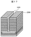
本発明に係る第6の実施例の撮像光学系の基本構成を図18Aに示す。実施例1〜実施例4の構成は、穴パターン計測を主な対象とするが、本実施の形態は、高アスペクト比の溝パターン(図17の185)を対象とする。例えば、3D−NANDプロセスにける、ワードラインのスリット形成工程がこれに相当する。本実施の形態では、撮像光学系004に、低角BSE検出のための検出器180として、方位角方向に分割した検出器180を用いる。
FIG. 18A shows the basic configuration of the image pickup optical system according to the sixth embodiment of the present invention. The configurations of Examples 1 to 4 are mainly intended for hole pattern measurement, but the present embodiment is intended for high aspect ratio groove patterns (185 in FIG. 17). For example, a word line slit forming step in a 3D-NAND process corresponds to this. In the present embodiment, a
計測対象が溝パターンの場合、溝の長手方向に放出されたBSEは、突き抜けBSEとはならないため、これを検出しないようにして、溝の短手方向に放出された、突き抜けBSEだけを検出するための検出器180が、図18Bに示すような4つの検出素子180a〜180dを備えた方位方向分割型の検出器180である。溝の方向に応じて、どの方位の検出器の出力を用いるかを選択する。
When the measurement target is a groove pattern, the BSE released in the longitudinal direction of the groove does not become a punch-through BSE. Therefore, only the punch-through BSE released in the short direction of the groove is detected without detecting this. The
図18Aに示した撮像光学系004を用いることにより、図17に示したような試料200に形成された溝パターン185の深さや溝幅の計測だけでなく、実施例1及び2で説明したような、穴パターンの深さや径の計測を行いことも可能である。
By using the imaging
本実施の形態によれば、高アスペクト比の溝パターンの計測に本発明であるところの、突き抜けBSE検出を適用することが可能となる。 According to the present embodiment, it is possible to apply the punch-through BSE detection, which is the present invention, to the measurement of a high aspect ratio groove pattern.
001,002,003,004・・・撮像光学系 021・・・制御部 022・・・演算部 023・・・記憶部 024・・・入出力部 101・・・電子銃 102・・・一次電子線 103・・・コンデンサレンズ 104・・・偏向器 105・・・対物レンズ 106・・・低角BSE検出用環状シンチレータ 108・・・ステージ 110・・・低角BSE 111・・・光ファイバ 112・・・光電子増倍管 113・・・低角BSE像を生成する画像生成部 200・・・試料 201、202・・・積層膜 204・・・正常に形成された穴パターン 205・・・ストッパ膜 206、207・・・穴開け不足のホール 208、209・・・穴開け過剰のホール 120・・・二次電子 121・・・二次電子検出器 122・・・二次電子像を生成する画像生成部 130・・・穴底から放射された二次電子 140・・・SE像上のホールパターン 141・・・低角BSE像上のホールパターン 150・・・高角BSE 151・・・高角BSE検出器 152・・・高角BSE像を生成する画像生成部 185・・・高アスペクトの溝パターン 180・・・方位方向分割型の低角BSE検出器。
001, 002, 003, 004 ... Imaging optical system 021 ...
Claims (14)
前記基板上に形成されたパターンに対して一次電子線を走査して照射する一次電子線照射手段と、
該一次電子線照射手段により一次電子線が照射された基板から放出される後方散乱電子のうち前記穴パターン又は溝パターンの側壁を突き抜けた後方散乱電子を検出する後方散乱電子検出手段と、
該後方散乱電子検出手段で検出した後方散乱電子の強度分布に対応する電子線像を生成する電子線像生成手段と、
該電子線像生成手段で生成した電子線像上の明部領域内に存在する暗部領域の前記明部領域との境界領域を求めて、該求めた境界領域の内部の暗部領域の明るさの情報から前記穴パターン又は溝パターンの深さを推定する深さ推定手段と
を有すことを特徴とする走査電子顕微鏡システム。 A system for measuring a hole pattern or a groove pattern formed on a substrate,
A primary electron beam irradiation means for scanning and irradiating a primary electron beam with respect to the pattern formed on the substrate;
Backscattered electron detection means for detecting backscattered electrons penetrating through the side walls of the hole pattern or groove pattern among the backscattered electrons emitted from the substrate irradiated with the primary electron beam by the primary electron beam irradiation means;
An electron beam image generation means for generating an electron beam image corresponding to the intensity distribution of the backscattered electrons detected by the backscattered electron detection means;
A boundary area between the dark area and the bright area existing in the bright area on the electron beam image generated by the electron beam image generating means is obtained, and the brightness of the dark area within the obtained boundary area is determined. A scanning electron microscope system comprising: a depth estimating unit that estimates the depth of the hole pattern or groove pattern from information.
前記基板上に形成されたパターンに対して一次電子線を走査して照射する一次電子線照射手段と、
該一次電子線照射手段により一次電子線が照射された基板から放出される後方散乱電子のうち前記穴パターン又は溝パターンの側壁を突き抜けた後方散乱電子を検出する後方散乱電子検出手段と、
該後方散乱電子検出手段で検出した後方散乱電子の強度分布に対応する電子線像を生成する電子線像生成手段と、
該電子線像生成手段で生成した電子線像上の明部領域内に存在する暗部領域の前記明部領域との境界領域を求めて、該求めた境界領域を前記穴パターン又は溝パターンのエッジ位置として検出する画像処理手段と、
前記電子線像生成手段で生成した電子線像上の前記明部領域内に存在する暗部領域の前記明部領域との境界領域を求めて、該求めた境界領域の内部の暗部領域の明るさの情報から前記穴パターン又は溝パターンの深さを推定する深さ推定手段と
を有すことを特徴とする走査電子顕微鏡システム。 A system for measuring a hole pattern or a groove pattern formed on a substrate,
A primary electron beam irradiation means for scanning and irradiating a primary electron beam with respect to the pattern formed on the substrate;
Backscattered electron detection means for detecting backscattered electrons penetrating through the side walls of the hole pattern or groove pattern among the backscattered electrons emitted from the substrate irradiated with the primary electron beam by the primary electron beam irradiation means;
An electron beam image generation means for generating an electron beam image corresponding to the intensity distribution of the backscattered electrons detected by the backscattered electron detection means;
A boundary area between the dark area and the bright area existing in the bright area on the electron beam image generated by the electron beam image generating means is obtained, and the obtained boundary area is defined as an edge of the hole pattern or groove pattern. Image processing means for detecting the position;
A boundary area between the dark area existing in the bright area on the electron beam image generated by the electron beam image generation unit and the bright area is determined, and the brightness of the dark area inside the determined boundary area is determined. And a depth estimating means for estimating the depth of the hole pattern or groove pattern from the above information.
前記後方散乱電子検出手段は、前記基板上に形成されたパターンに照射する一次電子線の光路を取り囲むようにして配置されて、前記一次電子線を走査して照射した前記基板から放出された後方散乱電子を検出する後方散乱電子検出器を備えていることを特徴とする走査電子顕微鏡システム。 A scanning electron microscope system according to any one of claims 1 to 2 ,
The backscattered electron detection means is disposed so as to surround the optical path of the primary electron beam that irradiates the pattern formed on the substrate, and the back emitted from the substrate irradiated by scanning the primary electron beam A scanning electron microscope system comprising a backscattered electron detector for detecting scattered electrons.
前記深さ推定手段は、予め作成した穴パターン又は溝パターンの深さと電子線像の明るさを関連づける検量線を参照して深さを算出することを特徴とする走査電子顕微鏡システム。 A scanning electron microscope system according to claim 1 or 2 ,
The depth estimation means calculates a depth by referring to a calibration curve that associates the depth of a hole pattern or groove pattern created in advance with the brightness of an electron beam image.
さらに、前記基板から放出される二次電子を検出する二次電子検出手段と、該二次電子検出手段で検出した二次電子の強度に対応する電子線像を生成する二次電子線像生成手段と、該二次電子線像生成手段で生成した二次電子の電子線像の前記明部領域のエッジ位置に基づき前記穴パターンの上径又は前記溝パターンの幅を計測するパターン幅計測手段を更に含むことを特徴とする走査電子顕微鏡システム。 A scanning electron microscope system according to any one of claims 1 to 2 ,
Further, secondary electron detection means for detecting secondary electrons emitted from the substrate, and secondary electron beam image generation for generating an electron beam image corresponding to the intensity of the secondary electrons detected by the secondary electron detection means And pattern width measuring means for measuring the upper diameter of the hole pattern or the width of the groove pattern based on the edge position of the bright area of the electron beam image of the secondary electrons generated by the secondary electron beam image generating means A scanning electron microscope system further comprising:
さらに、前記基板から放出される後方散乱電子のうち仰角が5度よりも小さい方向に散乱した後方散乱電子を検出する第二の後方散乱電子検出手段と、該第二の後方散乱電子検出手段で検出した仰角が5度よりも小さい方向に散乱した後方散乱電子強度に対応する電子線像を生成する第二の電子線像生成手段と、該第二の電子線像生成手段で生成した後方散乱電子線像上の前記穴パターン又は前記溝パターンの底相当領域の明るさから、前記穴パターン又は前記溝パターンの底の材料を推定する材料推定手段を更に含むことを特徴とする走査電子顕微鏡システム。 A scanning electron microscope system according to any one of claims 1 to 2 ,
Furthermore, a second backscattered electron detection means for detecting backscattered electrons scattered in a direction whose elevation angle is smaller than 5 degrees among the backscattered electrons emitted from the substrate, and the second backscattered electron detection means Second electron beam image generation means for generating an electron beam image corresponding to the backscattered electron intensity scattered in a direction in which the detected elevation angle is smaller than 5 degrees, and backscattering generated by the second electron beam image generation means A scanning electron microscope system further comprising a material estimating means for estimating a material of a bottom of the hole pattern or the groove pattern from brightness of a region corresponding to a bottom of the hole pattern or the groove pattern on an electron beam image .
前記穴パターン又は溝パターンの側壁を突き抜けた後方散乱電子を検出する前記後方散乱電子検出手段は、前記後方散乱電子を方位別に検出する複数の検出面を有する検出器を備えたことを特徴とする走査電子顕微鏡システム。 A scanning electron microscope system according to any one of claims 1 to 2 ,
The backscattered electron detection means for detecting backscattered electrons penetrating through the side wall of the hole pattern or groove pattern includes a detector having a plurality of detection surfaces for detecting the backscattered electrons according to orientation. Scanning electron microscope system.
電子顕微鏡で基板上に形成された穴パターン又は溝パターンに対して一次電子線を走査して照射し、
該一次電子線が照射された前記基板から放出される後方散乱電子のうち前記穴パターン又は溝パターンの側壁を突き抜けた後方散乱電子を検出し、
該検出した後方散乱電子の強度分布に対応する電子線像を生成し、
該生成した電子線像上の明部領域内に存在する暗部領域の前記明部領域との境界領域を求め、
該求めた境界領域を前記穴パターン又は溝パターンのエッジ位置として検出することと、前記求めた境界領域の内部の暗部領域の明るさの情報から前記穴パターン又は溝パターンの深さを推定することの何れか又は両方を行うことを特徴とする走査電子顕微鏡システムを用いたパターン計測方法。 A method for measuring a hole pattern or a groove pattern formed on a substrate,
Scanning and irradiating the primary electron beam to the hole pattern or groove pattern formed on the substrate with an electron microscope,
Detecting backscattered electrons penetrating the side wall of the hole pattern or groove pattern among the backscattered electrons emitted from the substrate irradiated with the primary electron beam;
Generating an electron beam image corresponding to the intensity distribution of the detected backscattered electrons,
Determining a boundary area between the dark area and the bright area existing in the bright area on the generated electron beam image;
Detecting the obtained boundary region as an edge position of the hole pattern or groove pattern, and estimating the depth of the hole pattern or groove pattern from information on the brightness of the dark area inside the obtained boundary region. A pattern measurement method using a scanning electron microscope system characterized by performing either or both of the above.
前記基板上に形成されたパターンに照射する一次電子線の光路を取り囲むようにして配置された後方散乱電子検出器が、前記一次電子線を走査して照射した前記基板から放出された後方散乱電子を検出することを特徴とする走査電子顕微鏡システムを用いたパターン計測方法。Backscattered electrons emitted from the substrate irradiated with a backscattered electron detector, which is arranged so as to surround the optical path of the primary electron beam irradiated on the pattern formed on the substrate, is scanned with the primary electron beam A pattern measurement method using a scanning electron microscope system characterized by
前記穴パターン又は前記溝パターンの前記深さの推定において、予め作成した穴パターン又は溝パターンの深さと電子線像の明るさを関連づける検量線を参照して深さを算出することを特徴とする走査電子顕微鏡システムを用いたパターン計測方法。In the estimation of the depth of the hole pattern or the groove pattern, the depth is calculated with reference to a calibration curve that associates the depth of the hole pattern or groove pattern created in advance with the brightness of the electron beam image. Pattern measurement method using a scanning electron microscope system.
さらに、前記基板から放出される二次電子を検出して、検出した該二次電子の強度に対応する電子線像を生成し、Further, secondary electrons emitted from the substrate are detected, and an electron beam image corresponding to the detected intensity of the secondary electrons is generated,
生成した該二次電子の電子線像の前記明部領域のエッジ位置に基づき前記穴パターンの上径又は前記溝パターンの幅を計測するThe upper diameter of the hole pattern or the width of the groove pattern is measured based on the edge position of the bright area of the generated electron beam image of the secondary electrons.
ことを特徴とする走査電子顕微鏡システムを用いたパターン計測方法。A pattern measuring method using a scanning electron microscope system.
さらに、前記基板から放出される後方散乱電子のうち仰角が5度よりも小さい方向に散乱した後方散乱電子を検出し、Further, backscattered electrons scattered from the substrate emitted in a direction whose elevation angle is smaller than 5 degrees are detected,
検出した該仰角が5度よりも小さい方向に散乱した後方散乱電子強度に対応する電子線像を生成し、Generating an electron beam image corresponding to the backscattered electron intensity scattered in a direction in which the detected elevation angle is smaller than 5 degrees;
生成した前記後方散乱電子強度に対応する前記電子線像上の前記穴パターン又は前記溝パターンの底相当領域の明るさから、前記穴パターン又は前記溝パターンの底の材料を推定するThe material of the bottom of the hole pattern or the groove pattern is estimated from the brightness of the region corresponding to the bottom of the hole pattern or the groove pattern on the electron beam image corresponding to the generated backscattered electron intensity.
ことを特徴とする走査電子顕微鏡システムを用いたパターン計測方法。A pattern measuring method using a scanning electron microscope system.
前記後方散乱電子を方位別に検出する複数の検出面を有する検出器が、前記穴パターン又は前記溝パターンの側壁を突き抜けた後方散乱電子を検出するA detector having a plurality of detection surfaces for detecting the backscattered electrons for each direction detects the backscattered electrons that have penetrated the side wall of the hole pattern or the groove pattern.
ことを特徴とする走査電子顕微鏡システムを用いたパターン計測方法。A pattern measuring method using a scanning electron microscope system.
Priority Applications (5)
| Application Number | Priority Date | Filing Date | Title |
|---|---|---|---|
| JP2013249249A JP6316578B2 (en) | 2013-12-02 | 2013-12-02 | Scanning electron microscope system, pattern measuring method using the same, and scanning electron microscope |
| TW103138407A TWI564926B (en) | 2013-12-02 | 2014-11-05 | Scanning electron microscopy system and the use of its pattern measurement method and scanning electron microscopy |
| PCT/JP2014/080661 WO2015083548A1 (en) | 2013-12-02 | 2014-11-19 | Scanning electron microscope system, pattern measurement method using same, and scanning electron microscope |
| US15/039,527 US9852881B2 (en) | 2013-12-02 | 2014-11-19 | Scanning electron microscope system, pattern measurement method using same, and scanning electron microscope |
| KR1020167006631A KR101762219B1 (en) | 2013-12-02 | 2014-11-19 | Scanning electron microscope system, pattern measurement method using same, and scanning electron microscope |
Applications Claiming Priority (1)
| Application Number | Priority Date | Filing Date | Title |
|---|---|---|---|
| JP2013249249A JP6316578B2 (en) | 2013-12-02 | 2013-12-02 | Scanning electron microscope system, pattern measuring method using the same, and scanning electron microscope |
Publications (3)
| Publication Number | Publication Date |
|---|---|
| JP2015106530A JP2015106530A (en) | 2015-06-08 |
| JP2015106530A5 JP2015106530A5 (en) | 2016-11-10 |
| JP6316578B2 true JP6316578B2 (en) | 2018-04-25 |
Family
ID=53273315
Family Applications (1)
| Application Number | Title | Priority Date | Filing Date |
|---|---|---|---|
| JP2013249249A Active JP6316578B2 (en) | 2013-12-02 | 2013-12-02 | Scanning electron microscope system, pattern measuring method using the same, and scanning electron microscope |
Country Status (5)
| Country | Link |
|---|---|
| US (1) | US9852881B2 (en) |
| JP (1) | JP6316578B2 (en) |
| KR (1) | KR101762219B1 (en) |
| TW (1) | TWI564926B (en) |
| WO (1) | WO2015083548A1 (en) |
Cited By (2)
| Publication number | Priority date | Publication date | Assignee | Title |
|---|---|---|---|---|
| KR20210018017A (en) * | 2019-08-07 | 2021-02-17 | 주식회사 히타치하이테크 | Scanning electron microscope and pattern measurement method |
| KR20210064361A (en) | 2018-11-05 | 2021-06-02 | 주식회사 히타치하이테크 | Pattern measurement methods, measurement systems, and computer-readable media |
Families Citing this family (35)
| Publication number | Priority date | Publication date | Assignee | Title |
|---|---|---|---|---|
| US9653257B2 (en) * | 2015-03-03 | 2017-05-16 | Kla-Tencor Corporation | Method and system for reducing charging artifacts in scanning electron microscopy images |
| JP6527799B2 (en) | 2015-09-25 | 2019-06-05 | 株式会社日立ハイテクノロジーズ | Charged particle beam device and pattern measurement device |
| JP6820660B2 (en) * | 2016-01-29 | 2021-01-27 | 株式会社日立ハイテク | Charged particle beam device |
| US10460903B2 (en) * | 2016-04-04 | 2019-10-29 | Kla-Tencor Corporation | Method and system for charge control for imaging floating metal structures on non-conducting substrates |
| WO2017179138A1 (en) | 2016-04-13 | 2017-10-19 | 株式会社 日立ハイテクノロジーズ | Pattern measurement device and pattern measurement method |
| WO2018020626A1 (en) * | 2016-07-28 | 2018-02-01 | 株式会社 日立ハイテクノロジーズ | Charged-particle beam apparatus |
| JP6640057B2 (en) * | 2016-09-14 | 2020-02-05 | 株式会社日立ハイテクノロジーズ | Electron microscope apparatus and method for measuring inclined hole using the same |
| JP2018113322A (en) | 2017-01-11 | 2018-07-19 | 株式会社日立国際電気 | Semiconductor device manufacturing method, program, and substrate processing apparatus |
| US11443915B2 (en) | 2017-09-26 | 2022-09-13 | Asml Netherlands B.V. | Detection of buried features by backscattered particles |
| KR102313921B1 (en) | 2017-10-13 | 2021-10-18 | 주식회사 히타치하이테크 | Pattern measuring device and pattern measuring method |
| JP6865465B2 (en) | 2017-11-10 | 2021-04-28 | 株式会社日立ハイテク | Pattern measuring device and measuring method |
| JP6541161B2 (en) * | 2017-11-17 | 2019-07-10 | 株式会社日立ハイテクサイエンス | Charged particle beam device |
| JP7137943B2 (en) * | 2018-03-20 | 2022-09-15 | 株式会社日立ハイテク | SEARCHING DEVICE, SEARCHING METHOD AND PLASMA PROCESSING DEVICE |
| JP2019185972A (en) * | 2018-04-06 | 2019-10-24 | 株式会社日立ハイテクノロジーズ | Scanning electron microscopy system and pattern depth measurement method |
| JP2019184354A (en) | 2018-04-06 | 2019-10-24 | 株式会社日立ハイテクノロジーズ | Electronic microscope device, inspection system using electronic microscope device, and inspection method using electronic microscope device |
| JP2019211356A (en) * | 2018-06-06 | 2019-12-12 | 株式会社日立ハイテクノロジーズ | Method for measuring pattern, pattern measurement tool, and computer readable medium |
| US10714306B2 (en) * | 2018-06-11 | 2020-07-14 | Applied Materials Israel Ltd. | Measuring a height profile of a hole formed in non-conductive region |
| US11515120B2 (en) | 2018-09-21 | 2022-11-29 | Hitachi High-Tech Corporation | Charged particle beam apparatus |
| JP7120873B2 (en) * | 2018-10-09 | 2022-08-17 | 株式会社日立製作所 | Measuring device and method for measuring surface of sample |
| JP7091263B2 (en) * | 2019-01-22 | 2022-06-27 | 株式会社日立ハイテク | Depth calculation method for electron microscope and 3D structure |
| JP7199290B2 (en) | 2019-04-08 | 2023-01-05 | 株式会社日立ハイテク | Pattern cross-sectional shape estimation system and program |
| WO2020225876A1 (en) * | 2019-05-08 | 2020-11-12 | 株式会社日立ハイテク | Pattern measurement device and measurement method |
| US11139142B2 (en) * | 2019-05-23 | 2021-10-05 | Applied Materials, Inc. | High-resolution three-dimensional profiling of features in advanced semiconductor devices in a non-destructive manner using electron beam scanning electron microscopy |
| KR20210027789A (en) * | 2019-09-03 | 2021-03-11 | 삼성전자주식회사 | Scanning electron microscope apparatus and operation method thereof |
| CN110751622B (en) * | 2019-09-05 | 2022-07-15 | 长江存储科技有限责任公司 | Method and device for detecting semiconductor structure |
| US10943763B1 (en) * | 2019-09-24 | 2021-03-09 | Applied Materials, Inc. | Use of electron beam scanning electron microscopy for characterization of a sidewall occluded from line-of-sight of the electron beam |
| CN112967941B (en) * | 2019-12-12 | 2022-04-26 | 长鑫存储技术有限公司 | Method, system and storage medium for detecting and feeding back inclination of capacitor hole |
| US11056404B1 (en) * | 2019-12-18 | 2021-07-06 | Applied Materials Israel Ltd. | Evaluating a hole formed in an intermediate product |
| US11335608B2 (en) | 2020-04-15 | 2022-05-17 | Kla Corporation | Electron beam system for inspection and review of 3D devices |
| JP2022015476A (en) | 2020-07-09 | 2022-01-21 | キオクシア株式会社 | Positional deviation measuring device, positional deviation measuring method, and positional deviation measuring program |
| CN112713113B (en) * | 2021-01-14 | 2022-05-24 | 长鑫存储技术有限公司 | Inclination angle prediction method and device, equipment monitoring method, medium and equipment |
| JP2022112137A (en) * | 2021-01-21 | 2022-08-02 | 株式会社日立ハイテク | Charged particle beam device |
| CN113466277B (en) * | 2021-06-25 | 2022-05-10 | 长江存储科技有限责任公司 | Preparation method of test sample and test sample |
| US11921063B2 (en) * | 2021-07-21 | 2024-03-05 | Applied Materials Israel Ltd. | Lateral recess measurement in a semiconductor specimen |
| CN113725113B (en) * | 2021-08-30 | 2023-11-10 | 长江存储科技有限责任公司 | Semiconductor device measuring method and device |
Family Cites Families (12)
| Publication number | Priority date | Publication date | Assignee | Title |
|---|---|---|---|---|
| JP3285092B2 (en) * | 1990-10-12 | 2002-05-27 | 株式会社日立製作所 | Scanning electron microscope and sample image forming method using scanning electron microscope |
| US5412210A (en) * | 1990-10-12 | 1995-05-02 | Hitachi, Ltd. | Scanning electron microscope and method for production of semiconductor device by using the same |
| JPH06310075A (en) * | 1993-04-27 | 1994-11-04 | Hitachi Ltd | Scanning electron microscope |
| JP3749107B2 (en) * | 1999-11-05 | 2006-02-22 | ファブソリューション株式会社 | Semiconductor device inspection equipment |
| JP2002110079A (en) * | 2000-09-29 | 2002-04-12 | Hitachi Ltd | Electron beam device |
| JP2003157790A (en) * | 2001-11-20 | 2003-05-30 | Advantest Corp | Micro ruggedness value measurement device and scanning electron microscope |
| WO2007067296A2 (en) * | 2005-12-02 | 2007-06-14 | Alis Corporation | Ion sources, systems and methods |
| JP2010175249A (en) * | 2009-01-27 | 2010-08-12 | Hitachi High-Technologies Corp | Method and device for measuring height of sample |
| WO2012039206A1 (en) * | 2010-09-25 | 2012-03-29 | 株式会社日立ハイテクノロジーズ | Charged particle beam microscope |
| JP5677236B2 (en) * | 2011-08-22 | 2015-02-25 | 株式会社日立ハイテクノロジーズ | Charged particle beam equipment |
| JP5814741B2 (en) * | 2011-10-20 | 2015-11-17 | 株式会社日立ハイテクノロジーズ | Scanning electron microscope |
| JP5787746B2 (en) * | 2011-12-26 | 2015-09-30 | 株式会社東芝 | Signal processing method and signal processing apparatus |
-
2013
- 2013-12-02 JP JP2013249249A patent/JP6316578B2/en active Active
-
2014
- 2014-11-05 TW TW103138407A patent/TWI564926B/en active
- 2014-11-19 WO PCT/JP2014/080661 patent/WO2015083548A1/en active Application Filing
- 2014-11-19 US US15/039,527 patent/US9852881B2/en active Active
- 2014-11-19 KR KR1020167006631A patent/KR101762219B1/en active IP Right Grant
Cited By (8)
| Publication number | Priority date | Publication date | Assignee | Title |
|---|---|---|---|---|
| KR20210064361A (en) | 2018-11-05 | 2021-06-02 | 주식회사 히타치하이테크 | Pattern measurement methods, measurement systems, and computer-readable media |
| TWI739196B (en) * | 2018-11-05 | 2021-09-11 | 日商日立全球先端科技股份有限公司 | Pattern measuring method, measuring system, and computer readable medium |
| JPWO2020095346A1 (en) * | 2018-11-05 | 2021-10-07 | 株式会社日立ハイテク | Pattern measurement methods, measurement systems, and computer-readable media |
| JP7150049B2 (en) | 2018-11-05 | 2022-10-07 | 株式会社日立ハイテク | PATTERN MEASUREMENT METHOD, MEASUREMENT SYSTEM, AND COMPUTER-READABLE MEDIUM |
| JP2022179549A (en) * | 2018-11-05 | 2022-12-02 | 株式会社日立ハイテク | Pattern measurement method, measurement system, and computer readable medium |
| JP7411042B2 (en) | 2018-11-05 | 2024-01-10 | 株式会社日立ハイテク | Pattern measurement method, measurement system, and computer readable medium |
| KR20210018017A (en) * | 2019-08-07 | 2021-02-17 | 주식회사 히타치하이테크 | Scanning electron microscope and pattern measurement method |
| KR102410882B1 (en) | 2019-08-07 | 2022-06-21 | 주식회사 히타치하이테크 | Scanning electron microscope and pattern measurement method |
Also Published As
| Publication number | Publication date |
|---|---|
| TWI564926B (en) | 2017-01-01 |
| TW201532101A (en) | 2015-08-16 |
| JP2015106530A (en) | 2015-06-08 |
| WO2015083548A1 (en) | 2015-06-11 |
| KR20160046837A (en) | 2016-04-29 |
| US9852881B2 (en) | 2017-12-26 |
| KR101762219B1 (en) | 2017-07-27 |
| US20160379798A1 (en) | 2016-12-29 |
Similar Documents
| Publication | Publication Date | Title |
|---|---|---|
| JP6316578B2 (en) | Scanning electron microscope system, pattern measuring method using the same, and scanning electron microscope | |
| CN109765254B (en) | Pattern measuring apparatus and measuring method | |
| WO2017051621A1 (en) | Charged particle beam device and pattern measurement device | |
| US9536700B2 (en) | Sample observation device | |
| US8604431B2 (en) | Pattern-height measuring apparatus and pattern-height measuring method | |
| US11545336B2 (en) | Scanning electron microscopy system and pattern depth measurement method | |
| JP2010175249A (en) | Method and device for measuring height of sample | |
| JPWO2017179138A1 (en) | Pattern measuring apparatus and pattern measuring method | |
| JP5932428B2 (en) | Scanning electron microscope | |
| JP2015146283A (en) | Charged particle beam device, and image generating method | |
| US11211226B2 (en) | Pattern cross-sectional shape estimation system and program | |
| US20210404801A1 (en) | Pattern Measurement Method, Measurement System, and Computer-Readable Medium | |
| US11302513B2 (en) | Electron microscope apparatus, inspection system using electron microscope apparatus, and inspection method using electron microscope apparatus | |
| US10903041B2 (en) | Pattern measuring method, pattern measuring tool and computer readable medium | |
| JPH08329875A (en) | Scanning electron microscope and method of displaying specimen image therefor | |
| JP5619118B2 (en) | Charged particle beam equipment | |
| JP2016139531A (en) | Sample observation, inspection, measurement method, and scanning electron microscope | |
| WO2021085049A1 (en) | Charged particle beam device | |
| US11443914B2 (en) | Charged-particle beam device and cross-sectional shape estimation program |
Legal Events
| Date | Code | Title | Description |
|---|---|---|---|
| A521 | Request for written amendment filed |
Free format text: JAPANESE INTERMEDIATE CODE: A523 Effective date: 20160920 |
|
| A621 | Written request for application examination |
Free format text: JAPANESE INTERMEDIATE CODE: A621 Effective date: 20160920 |
|
| A131 | Notification of reasons for refusal |
Free format text: JAPANESE INTERMEDIATE CODE: A131 Effective date: 20170926 |
|
| A521 | Request for written amendment filed |
Free format text: JAPANESE INTERMEDIATE CODE: A523 Effective date: 20171011 |
|
| TRDD | Decision of grant or rejection written | ||
| A01 | Written decision to grant a patent or to grant a registration (utility model) |
Free format text: JAPANESE INTERMEDIATE CODE: A01 Effective date: 20180320 |
|
| A61 | First payment of annual fees (during grant procedure) |
Free format text: JAPANESE INTERMEDIATE CODE: A61 Effective date: 20180328 |
|
| R150 | Certificate of patent or registration of utility model |
Ref document number: 6316578 Country of ref document: JP Free format text: JAPANESE INTERMEDIATE CODE: R150 |
|
| S531 | Written request for registration of change of domicile |
Free format text: JAPANESE INTERMEDIATE CODE: R313531 |
|
| S533 | Written request for registration of change of name |
Free format text: JAPANESE INTERMEDIATE CODE: R313533 |
|
| R350 | Written notification of registration of transfer |
Free format text: JAPANESE INTERMEDIATE CODE: R350 |