JP6305686B2 - Power receiving device and power feeding system - Google Patents
Power receiving device and power feeding system Download PDFInfo
- Publication number
- JP6305686B2 JP6305686B2 JP2013061580A JP2013061580A JP6305686B2 JP 6305686 B2 JP6305686 B2 JP 6305686B2 JP 2013061580 A JP2013061580 A JP 2013061580A JP 2013061580 A JP2013061580 A JP 2013061580A JP 6305686 B2 JP6305686 B2 JP 6305686B2
- Authority
- JP
- Japan
- Prior art keywords
- power
- potential
- communication
- terminal
- circuit
- Prior art date
- Legal status (The legal status is an assumption and is not a legal conclusion. Google has not performed a legal analysis and makes no representation as to the accuracy of the status listed.)
- Active
Links
- 238000004891 communication Methods 0.000 claims description 108
- 230000005540 biological transmission Effects 0.000 claims description 60
- 238000009499 grossing Methods 0.000 claims description 25
- 238000010168 coupling process Methods 0.000 description 34
- 230000008878 coupling Effects 0.000 description 33
- 238000005859 coupling reaction Methods 0.000 description 33
- 239000003990 capacitor Substances 0.000 description 19
- 238000000034 method Methods 0.000 description 6
- 230000001413 cellular effect Effects 0.000 description 4
- 230000008859 change Effects 0.000 description 4
- 230000005674 electromagnetic induction Effects 0.000 description 4
- 230000009471 action Effects 0.000 description 3
- 238000007599 discharging Methods 0.000 description 2
- 238000005259 measurement Methods 0.000 description 2
- 230000001902 propagating effect Effects 0.000 description 2
- 238000009774 resonance method Methods 0.000 description 2
- 230000004044 response Effects 0.000 description 2
- 239000000470 constituent Substances 0.000 description 1
- 238000010586 diagram Methods 0.000 description 1
- 238000005516 engineering process Methods 0.000 description 1
- 238000012545 processing Methods 0.000 description 1
- 230000002250 progressing effect Effects 0.000 description 1
- 230000003252 repetitive effect Effects 0.000 description 1
- 238000012827 research and development Methods 0.000 description 1
- 230000007480 spreading Effects 0.000 description 1
Images


Classifications
-
- H04B5/79—
-
- B—PERFORMING OPERATIONS; TRANSPORTING
- B60—VEHICLES IN GENERAL
- B60L—PROPULSION OF ELECTRICALLY-PROPELLED VEHICLES; SUPPLYING ELECTRIC POWER FOR AUXILIARY EQUIPMENT OF ELECTRICALLY-PROPELLED VEHICLES; ELECTRODYNAMIC BRAKE SYSTEMS FOR VEHICLES IN GENERAL; MAGNETIC SUSPENSION OR LEVITATION FOR VEHICLES; MONITORING OPERATING VARIABLES OF ELECTRICALLY-PROPELLED VEHICLES; ELECTRIC SAFETY DEVICES FOR ELECTRICALLY-PROPELLED VEHICLES
- B60L53/00—Methods of charging batteries, specially adapted for electric vehicles; Charging stations or on-board charging equipment therefor; Exchange of energy storage elements in electric vehicles
- B60L53/10—Methods of charging batteries, specially adapted for electric vehicles; Charging stations or on-board charging equipment therefor; Exchange of energy storage elements in electric vehicles characterised by the energy transfer between the charging station and the vehicle
- B60L53/12—Inductive energy transfer
- B60L53/122—Circuits or methods for driving the primary coil, e.g. supplying electric power to the coil
-
- H—ELECTRICITY
- H02—GENERATION; CONVERSION OR DISTRIBUTION OF ELECTRIC POWER
- H02J—CIRCUIT ARRANGEMENTS OR SYSTEMS FOR SUPPLYING OR DISTRIBUTING ELECTRIC POWER; SYSTEMS FOR STORING ELECTRIC ENERGY
- H02J50/00—Circuit arrangements or systems for wireless supply or distribution of electric power
- H02J50/20—Circuit arrangements or systems for wireless supply or distribution of electric power using microwaves or radio frequency waves
-
- H—ELECTRICITY
- H02—GENERATION; CONVERSION OR DISTRIBUTION OF ELECTRIC POWER
- H02J—CIRCUIT ARRANGEMENTS OR SYSTEMS FOR SUPPLYING OR DISTRIBUTING ELECTRIC POWER; SYSTEMS FOR STORING ELECTRIC ENERGY
- H02J50/00—Circuit arrangements or systems for wireless supply or distribution of electric power
- H02J50/80—Circuit arrangements or systems for wireless supply or distribution of electric power involving the exchange of data, concerning supply or distribution of electric power, between transmitting devices and receiving devices
-
- H04B5/266—
-
- Y—GENERAL TAGGING OF NEW TECHNOLOGICAL DEVELOPMENTS; GENERAL TAGGING OF CROSS-SECTIONAL TECHNOLOGIES SPANNING OVER SEVERAL SECTIONS OF THE IPC; TECHNICAL SUBJECTS COVERED BY FORMER USPC CROSS-REFERENCE ART COLLECTIONS [XRACs] AND DIGESTS
- Y02—TECHNOLOGIES OR APPLICATIONS FOR MITIGATION OR ADAPTATION AGAINST CLIMATE CHANGE
- Y02T—CLIMATE CHANGE MITIGATION TECHNOLOGIES RELATED TO TRANSPORTATION
- Y02T10/00—Road transport of goods or passengers
- Y02T10/60—Other road transportation technologies with climate change mitigation effect
- Y02T10/70—Energy storage systems for electromobility, e.g. batteries
-
- Y—GENERAL TAGGING OF NEW TECHNOLOGICAL DEVELOPMENTS; GENERAL TAGGING OF CROSS-SECTIONAL TECHNOLOGIES SPANNING OVER SEVERAL SECTIONS OF THE IPC; TECHNICAL SUBJECTS COVERED BY FORMER USPC CROSS-REFERENCE ART COLLECTIONS [XRACs] AND DIGESTS
- Y02—TECHNOLOGIES OR APPLICATIONS FOR MITIGATION OR ADAPTATION AGAINST CLIMATE CHANGE
- Y02T—CLIMATE CHANGE MITIGATION TECHNOLOGIES RELATED TO TRANSPORTATION
- Y02T10/00—Road transport of goods or passengers
- Y02T10/60—Other road transportation technologies with climate change mitigation effect
- Y02T10/7072—Electromobility specific charging systems or methods for batteries, ultracapacitors, supercapacitors or double-layer capacitors
-
- Y—GENERAL TAGGING OF NEW TECHNOLOGICAL DEVELOPMENTS; GENERAL TAGGING OF CROSS-SECTIONAL TECHNOLOGIES SPANNING OVER SEVERAL SECTIONS OF THE IPC; TECHNICAL SUBJECTS COVERED BY FORMER USPC CROSS-REFERENCE ART COLLECTIONS [XRACs] AND DIGESTS
- Y02—TECHNOLOGIES OR APPLICATIONS FOR MITIGATION OR ADAPTATION AGAINST CLIMATE CHANGE
- Y02T—CLIMATE CHANGE MITIGATION TECHNOLOGIES RELATED TO TRANSPORTATION
- Y02T90/00—Enabling technologies or technologies with a potential or indirect contribution to GHG emissions mitigation
- Y02T90/10—Technologies relating to charging of electric vehicles
- Y02T90/14—Plug-in electric vehicles
-
- Y—GENERAL TAGGING OF NEW TECHNOLOGICAL DEVELOPMENTS; GENERAL TAGGING OF CROSS-SECTIONAL TECHNOLOGIES SPANNING OVER SEVERAL SECTIONS OF THE IPC; TECHNICAL SUBJECTS COVERED BY FORMER USPC CROSS-REFERENCE ART COLLECTIONS [XRACs] AND DIGESTS
- Y02—TECHNOLOGIES OR APPLICATIONS FOR MITIGATION OR ADAPTATION AGAINST CLIMATE CHANGE
- Y02T—CLIMATE CHANGE MITIGATION TECHNOLOGIES RELATED TO TRANSPORTATION
- Y02T90/00—Enabling technologies or technologies with a potential or indirect contribution to GHG emissions mitigation
- Y02T90/10—Technologies relating to charging of electric vehicles
- Y02T90/16—Information or communication technologies improving the operation of electric vehicles
Description
開示される発明の一態様は、受電装置及び給電システムに関する。 One embodiment of the disclosed invention relates to a power receiving device and a power feeding system.
様々な電子機器の普及が進み、多種多様な製品が市場に出荷されている。近年では、携帯電話及びデジタルビデオカメラ等の携帯型の電子機器の普及が顕著である。また電力を基に動力を得る電気自動車等の電気推進移動体も製品として市場に登場しつつある。 Various electronic devices are spreading and various products are shipped to the market. In recent years, portable electronic devices such as mobile phones and digital video cameras have been widely used. In addition, electric propulsion vehicles such as electric vehicles that obtain power based on electric power are also appearing on the market as products.
携帯電話、デジタルビデオカメラまたは電気推進移動体には、蓄電手段である蓄電装置(バッテリ、蓄電池ともいう)が内蔵されている。当該蓄電装置の給電は、殆どが給電手段である家庭用交流電源より直接的に接触させて行われているのが現状である。また蓄電装置を具備しない構成または蓄電装置に給電された電力を用いない構成では、家庭用交流電源より配線等を介して直接給電し動作させているのが現状である。 A mobile phone, a digital video camera, or an electric propulsion mobile body includes a power storage device (also referred to as a battery or a storage battery) that is a power storage unit. At present, power is supplied to the power storage device in direct contact with a home AC power source as a power supply means. Further, in a configuration in which the power storage device is not provided or a configuration in which power supplied to the power storage device is not used, the current situation is that power is directly supplied from a household AC power supply via a wiring or the like.
一方で非接触により蓄電装置の給電または負荷への給電を行う方式についての研究開発も進んでおり、代表的な方式として、電磁結合方式(電磁誘導方式ともいう)(特許文献1及び特許文献2参照)、電波方式(マイクロ波方式ともいう)、磁界共鳴方式(共振方式ともいう)(特許文献3及び特許文献4参照)が挙げられる。
On the other hand, research and development on a method for supplying power to a power storage device or supplying power to a load in a non-contact manner is also progressing. As a representative method, an electromagnetic coupling method (also referred to as an electromagnetic induction method) (
特許文献3に示されるように、磁界共鳴方式の非接触給電技術においては、電力を受ける側の装置(以下、受電装置という)及び電力を供給する側の装置(以下、送電装置という)のそれぞれが、共鳴コイルを有している。また受電装置及び送電装置には、それぞれ電磁誘導コイルが設けられている。送電装置における電源から共鳴コイルへの給電、及び、受電装置における共鳴コイルから負荷への給電は、電磁誘導コイルを介して行われる。
As shown in
送電装置は、共鳴コイルとコンデンサを含む第1のLC共振回路を有する。受電装置は、共鳴コイルとコンデンサを含む第2のLC共振回路を有する。第1のLC共振回路と第2のLC共振回路は、特定の周波数で磁気共鳴現象が発現するよう、それぞれの共振周波数(LC共振)が調整されている。 The power transmission device has a first LC resonance circuit including a resonance coil and a capacitor. The power receiving apparatus includes a second LC resonance circuit including a resonance coil and a capacitor. The first LC resonance circuit and the second LC resonance circuit have their resonance frequencies (LC resonance) adjusted so that the magnetic resonance phenomenon appears at a specific frequency.
これら送電装置の共鳴コイル及び受電装置の共鳴コイルが対向し、磁界共鳴現象を起こすことにより、当該共鳴コイル間距離が離れている状態でも、効率の良い電力伝送が実現できる(非特許文献1参照)。 The resonance coil of the power transmission device and the resonance coil of the power reception device face each other and cause a magnetic field resonance phenomenon, so that efficient power transmission can be realized even when the distance between the resonance coils is long (see Non-Patent Document 1). ).
特許文献1乃至特許文献4に記載の電力伝送システムでは、電力伝送と共に、受電側の情報を送電側に伝える通信を、受電側のアンテナ及び送電側のアンテナを用いて行っている。
In the power transmission systems described in
通信と電力伝送を同じ送電側アンテナ及び受電側アンテナで行うと、通信期間(小さい電力で行う)及び給電期間(大きな電力で行う)を、時間的に分離しなくてはならない。そのため、通信中は給電が行えず、また給電中は通信を行えないという状況が発生する。 When communication and power transmission are performed by the same power transmission side antenna and power reception side antenna, the communication period (performed with small power) and the power feeding period (performed with large power) must be separated in time. Therefore, a situation occurs where power cannot be supplied during communication, and communication cannot be performed during power supply.
通信と給電を時間的に分離してしまうと、給電中に通信(データ送受信)を行えなくなり、データ送受信のタイミングの自由度が著しく低下する。そのため、受信側の情報(例えば、受電側の入力電力の電力値や、受電側に設けられた蓄電装置の充電電圧値等)の伝達遅延を招く恐れを生じる。 If communication and power supply are separated in time, communication (data transmission / reception) cannot be performed during power supply, and the degree of freedom in data transmission / reception timing is significantly reduced. Therefore, there is a possibility that transmission delay of information on the reception side (for example, the power value of the input power on the power reception side, the charging voltage value of the power storage device provided on the power reception side, etc.) may occur.
また通信と給電を時間的に分離してしまうと、通信中は給電を行うことができないため、受電側は継続的に電力を受け取ることができない。 If communication and power supply are separated in time, power supply cannot be performed during communication, and the power receiving side cannot continuously receive power.
通信中は給電を行うことができないと、直接コードから充電するような接点型充電方式での充電と比較して、蓄電装置への充電速度は低下する。 If power cannot be supplied during communication, the charging speed of the power storage device is reduced as compared with charging by a contact-type charging method in which charging is performed directly from a cord.
また、受電側が受け取った電力を、負荷(例えば、電気機器)で消費する場合、電力供給されない期間が発生すると、当該負荷(例えば、電気機器)が動作できないという恐れが生じる。 Further, when the power received by the power receiving side is consumed by a load (for example, an electric device), if a period in which the power is not supplied occurs, there is a fear that the load (for example, the electric device) cannot be operated.
以上に鑑みて、開示される発明の一態様は、通信及び給電を同時に行うことが可能な受電装置及び給電システムを提供することを課題の一とする。 In view of the above, an object of one embodiment of the disclosed invention is to provide a power receiving device and a power feeding system capable of performing communication and power feeding at the same time.
また通信と給電を同時に行うと、通信の電磁波の基準電位と、給電の直流電力の基準電位がずれてしまい、通信の電磁波の基準電位が不安定化するという恐れがある。通信の電磁波の基準電位が不安定化すると、通信自体が不可能になる恐れが生じる。 If communication and power feeding are performed simultaneously, the reference potential of electromagnetic waves for communication and the reference potential of DC power for feeding may be shifted, and the reference potential of electromagnetic waves for communication may become unstable. If the reference potential of electromagnetic waves for communication becomes unstable, there is a possibility that communication itself becomes impossible.
よって開示される発明の一態様では、給電中も安定な通信が行える受電装置及び給電システムを提供することを課題の一とする。 Thus, an object of one embodiment of the disclosed invention is to provide a power receiving device and a power feeding system that can perform stable communication even during power feeding.
通信及び給電を同時に行う給電システムにおいて、受電装置のアンテナが交流電力を受電後、当該受電した交流電力に含まれていた変調信号を通信制御部へ送り、当該通信制御部の制御回路が当該変調信号を解析する。これにより、当該変調信号に含まれる送電装置の情報や指示を受電装置が受信することができる。 In a power feeding system that performs communication and power feeding simultaneously, after the antenna of the power receiving apparatus receives AC power, the modulation signal included in the received AC power is sent to the communication control unit, and the control circuit of the communication control unit performs the modulation. Analyze the signal. Thereby, the power receiving apparatus can receive information and instructions of the power transmitting apparatus included in the modulation signal.
また当該受電した交流電力は、整流回路によって整流され、直流電力に変換される。当該直流電力は、受電装置に設置されている蓄電装置に蓄えられる。蓄電装置に蓄えられた直流電力の一部は、当該通信制御部を駆動する電力として用いられる。 The received AC power is rectified by a rectifier circuit and converted to DC power. The DC power is stored in a power storage device installed in the power receiving device. A part of the DC power stored in the power storage device is used as power for driving the communication control unit.
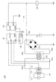
通信及び給電を同時に行うことが可能な受電装置を、図3に示す。図3に示す受電装置130は、アンテナである電磁結合コイル113、整流回路115、平滑化回路116、蓄電装置120、通信制御部119を有している。
FIG. 3 illustrates a power receiving device that can perform communication and power feeding at the same time. A
電磁結合コイル113の一方の端子、整流回路115の第1の端子、及び通信制御部119の端子Tx1は、ノードNDaと電気的に接続されている。電磁結合コイル113の他方の端子、整流回路115の第2の端子、及び通信制御部119の端子Tx2は、ノードNDbと電気的に接続されている。電磁結合コイル113の中心点は、通信制御部119の端子COMに電気的に接続されている。
One terminal of the
整流回路115の第3の端子、平滑化回路116の第1の端子、蓄電装置120の正極、通信制御部119の端子VBatは、ノードNDcと電気的に接続されている。整流回路115の第4の端子は、接地されている。
The third terminal of the
整流回路115は、交流電力を直流電力に変換する交流−直流変換器(AC−DCコンバータ)として機能する。高い整流効率を得るためには、整流回路115として全波整流を用いることが好適である。図3に示す整流回路115は、4つのダイオードから構成されるブリッジ整流回路である。
The
平滑化回路116は、整流回路115から出力された直流電力を蓄え、かつ放出することにより、直流電力を平滑化する機能を有する。図3の受電装置130において、平滑化回路116としてコンデンサを用いる。また、平滑化回路116の第2の端子は、接地されている。なお平滑化回路116は、必要がなければ設けなくてもよい。
The
蓄電装置120は、直流電力を蓄える機能を有する。蓄電装置120の正極は、ノードNDcに電気的に接続され、負極は、接地されている。
The
通信制御部119は、送電装置から受電装置へ送電される交流電力に含まれる変調信号(送信信号)を解析する。通信制御部119は、入力された交流電力の電圧振幅の振幅変調を読み取ることで、変調信号を解析する。これにより、当該変調信号に含まれる送電装置の情報や指示を受電装置が受信することができる。
The
なお、変調信号(送信信号)を含む交流電力を受信した受電装置130は、送電装置(図示しない)へ反射電力を反射する。当該反射電力には、受電装置130の情報を含む変調信号(返信信号)が含まれている。当該返信信号を含む反射電力を受信し、当該返信信号を解析することにより、送電装置は受電装置130の情報を得ることができる。これにより、送電装置及び受電装置130間の通信が成立する。
Note that the
通信制御部119の端子GNDには、接地電位GNDが印加される。通信制御部119の端子VBatに印加される電位VBat、及び、端子GNDに印加される接地電位GNDを基準電位として、通信制御部119が駆動される。
The ground potential GND is applied to the terminal GND of the
一方、通信制御部119の端子Tx1及び端子Tx2には、受電装置のアンテナが受電した電磁波としての交流電力が入力される。
On the other hand, AC power as an electromagnetic wave received by the antenna of the power receiving apparatus is input to the terminal Tx1 and the terminal Tx2 of the
ここで、整流回路115によって整流される前の交流電力の電圧振幅と、整流回路115によって整流された後の直流電力の最大電位及び最小電位を図2(A)に示す。なお、図2(A)乃至図2(C)の横軸は時間であり、縦軸は電位である。ノードNDa、ノードNDb、及びノードNDcの電位を、それぞれ電位Va、電位Vb、及び電位Vcとする。整流回路115によって整流された後の直流電力の電位Vc及び接地電位である電位GNDは、上述のように、通信制御部119を駆動する際の基準電位として機能する。
Here, FIG. 2A illustrates the voltage amplitude of the AC power before being rectified by the
なお受電装置130のアンテナが受電した交流電力は、後述の交流電源で生成された交流電力(搬送波)を変調した電力(電磁波)である。そのため、当該変調した電力(電磁波)を整流することによって得られた直流電力の電位は、最大値が電位Vaより低い電位Vcとなり、最小値が接地電位となる。平滑化回路116により整流後の直流電力が平滑化され、蓄電装置120に充電される。蓄電装置120への充電電力の最大電位は電位Vc、最小電位は電位GNDとみなすことができる。別言すれば、蓄電装置への充電電圧はVc−GNDであるとみなすことが可能である。
Note that the AC power received by the antenna of the
図2(A)に示すように、受電装置130のアンテナ(電磁結合コイル113)が受電した交流電力Aは、最大電位である電位Va及び最小電位である電位Vbを有する電磁波である。当該交流電力を整流回路115によって整流すると、受電装置130のアンテナの中心点の電位Vmを基準電位として、プラス側に電位Vcを有する直流電力が発生する。なお本明細書では、アンテナの中心点の電位Vmは、電位Vaと電位Vbの差の中間の電位を有するので、電位Vmを交流電力の中間電位ともいう。
As shown in FIG. 2A, AC power A received by the antenna (electromagnetic coupling coil 113) of the
上述のようにして生成された直流電力により通信制御部119が駆動される場合、通信制御部119の端子VBatに電位Vcが印加される。
When the
また、上述のように、最大電位である電位Va、最小電位である電位Vbを有し、変調信号を有する交流電力Aは、通信制御部119の端子Tx1、端子Tx2に入力される。この時、通信制御部119内部の電位変動の影響を受けて、交流電力の基準電位Vmが変動する場合がある(図2(B)参照)。
Further, as described above, the AC power A having the potential Va which is the maximum potential and the potential Vb which is the minimum potential and having the modulation signal is input to the terminal Tx1 and the terminal Tx2 of the
例えば、図2(B)において、最大電位である電位Va、最小電位である電位Vb、及び基準電位である電位Vmを有する交流電力を交流電力Aとし、基準電位が変動して電位Vm1となった後の交流電力を交流電力Bとする。交流電力Bは、基準電位である電位Vm1(Vm1<Vm)、最大電位である電位Va’(Va’<Va)、最小電位である電位Vb’(Vb’<Vb)を有する交流電力である。 For example, in FIG. 2B, AC power having the potential Va that is the maximum potential, the potential Vb that is the minimum potential, and the potential Vm that is the reference potential is defined as AC power A, and the reference potential varies to become the potential Vm1. The AC power after this is referred to as AC power B. The AC power B is AC power having a reference potential Vm1 (Vm1 <Vm), a maximum potential Va ′ (Va ′ <Va), and a minimum potential Vb ′ (Vb ′ <Vb). .
交流電力Bのような交流電力が整流回路115に供給されると、生成されるノードNDcの電位は、電位Vcより低い電位である電位Vc’となる。なお、電位Vm1が電位Vmよりも高い場合は、電位Vc’は電位Vcより高くなる。このように、整流回路115に入力される交流電力の基準電位が不安定であると、生成される電位Vcが不安定となり、通信に支障を来す恐れが生じる。さらには、通信制御系の駆動回路の破損を招く恐れが生じる。
When AC power such as AC power B is supplied to the
安定な通信を得るために、さらに、通信制御系の駆動回路の破損を防ぐために、開示される発明の一態様では、通信制御部119内部の電位変動の影響を受けないように、整流回路115に交流電力を入力する。より具体的には、受電装置のアンテナ及び整流回路との間に変圧器(トランスともいう)を配置する。
In order to obtain stable communication and to prevent damage to the drive circuit of the communication control system, in one embodiment of the disclosed invention, the
受電装置のアンテナ及び整流回路との間に変圧器を配置すると、アンテナから通信制御部119に入力された交流電力(変調信号を含む)が通信制御部119内部の電位変動の影響を受けたとしても、変圧器は電圧振幅のみを伝達するため、電位Vcを安定させることができる。
When a transformer is arranged between the antenna and the rectifier circuit of the power receiving apparatus, the AC power (including the modulation signal) input from the antenna to the
以上により、開示される発明の一態様の受電装置及び給電システムにおいて、安定な通信を得ることができる。さらに、開示される発明の一態様の受電装置及び給電システムにおいて、通信制御系の駆動回路の破損を防ぐことが可能となる。 As described above, stable communication can be obtained in the power receiving device and the power feeding system of one embodiment of the disclosed invention. Furthermore, in the power receiving device and the power feeding system of one embodiment of the disclosed invention, it is possible to prevent damage to the drive circuit of the communication control system.
開示される発明の一態様は、変調信号を含む交流電力を受信する、通信用及び給電用アンテナと、当該受信した変調信号を含む交流電力を整流することにより、当該変調信号を含む交流電力を直流電力に変換する整流回路と、当該変換された直流電力を平滑する平滑化回路と、当該平滑化された直流電力を蓄える蓄電装置と、当該変調信号を含む交流電力が入力され、当該交流電力に含まれる変調信号を解析し、当該直流電力の電位及び接地電位を用いて駆動される通信制御部と、当該アンテナと当該整流回路との間に配置され、当該通信制御部に入力される当該交流電力の基準電位を変化させる変圧器と、を有することを特徴とする受電装置に関する。 According to one embodiment of the disclosed invention, AC power including a modulation signal is obtained by rectifying AC power including a communication antenna and a power feeding antenna that receive AC power including a modulation signal and the received modulation signal. A rectifier circuit for converting to DC power, a smoothing circuit for smoothing the converted DC power, a power storage device for storing the smoothed DC power, and AC power including the modulation signal are input, and the AC power The modulation signal included in the signal is analyzed, and the communication control unit that is driven by using the potential of the DC power and the ground potential is disposed between the antenna and the rectifier circuit, and is input to the communication control unit. And a transformer for changing a reference potential of AC power.
開示される発明の一態様において、当該通信制御部は、当該変調信号を解析する制御回路と、当該変調信号を当該制御回路が解析可能な信号に変換する無線インターフェース部と、当該直流電力の電位及び接地電位から、当該制御回路及び当該無線インターフェース部の基準電位を生成するリファレンス電圧生成部を有することを特徴とする。 In one embodiment of the disclosed invention, the communication control unit includes a control circuit that analyzes the modulation signal, a wireless interface unit that converts the modulation signal into a signal that can be analyzed by the control circuit, and a potential of the DC power. And a reference voltage generation unit that generates a reference potential of the control circuit and the wireless interface unit from the ground potential.
開示される発明の一態様は、変調信号を生成する第1の制御回路と、当該変調信号を無線通信可能な信号に変換する変調回路と、当該変調信号を含む交流電力を送信する第1のアンテナと、を有する送信装置と、当該変調信号を含む交流電力を受信する、通信用及び給電用の第2のアンテナと、当該第2のアンテナが受信した当該変調信号を含む交流電力を整流することにより、当該変調信号を含む交流電力を直流電力に変換する整流回路と、当該変換された直流電力を平滑する平滑化回路と、当該平滑化された直流電力を蓄える蓄電装置と、当該当該変調信号を含む交流電力が入力され、当該交流電力に含まれる当該変調信号を解析し、当該直流電力の電位及び接地電位を用いて駆動される通信制御部と、当該第2のアンテナと当該整流回路との間に配置され、当該通信制御部に入力される当該交流電力の一部の基準電位を変化させる変圧器と、を有する受電装置と、を有することを特徴とする給電システムに関する。 One embodiment of the disclosed invention includes a first control circuit that generates a modulation signal, a modulation circuit that converts the modulation signal into a signal that can be wirelessly communicated, and a first circuit that transmits AC power including the modulation signal. A transmitter having an antenna; a second antenna for communication and power supply that receives AC power including the modulation signal; and rectifying AC power including the modulation signal received by the second antenna. A rectifier circuit that converts AC power including the modulation signal into DC power, a smoothing circuit that smoothes the converted DC power, a power storage device that stores the smoothed DC power, and the modulation AC power including a signal is input, the modulation signal included in the AC power is analyzed, a communication control unit driven using the potential of the DC power and the ground potential, the second antenna, and the rectifying circuit Is arranged between the concerns power supply system, characterized in that it comprises a transformer for changing the portion of the reference potential of the AC power input to the communication control unit, a power receiving device having, a.
開示される発明の一態様において、当該通信制御部は、当該変調信号を解析する第2の制御回路と、当該変調信号を当該第2の制御回路が解析可能な信号に変換する無線インターフェース部と、当該直流電力の電位及び接地電位から、当該第2の制御回路及び当該無線インターフェース部の基準電位を生成するリファレンス電圧生成部を有することを特徴とする。 In one embodiment of the disclosed invention, the communication control unit includes a second control circuit that analyzes the modulation signal, and a wireless interface unit that converts the modulation signal into a signal that can be analyzed by the second control circuit. And a reference voltage generating unit that generates a reference potential of the second control circuit and the wireless interface unit from the potential of the DC power and the ground potential.
開示される発明の一態様により、通信及び給電を同時に行うことが可能な受電装置及び給電システムを提供することができる。 According to one embodiment of the disclosed invention, a power receiving device and a power feeding system that can perform communication and power feeding at the same time can be provided.
また開示される発明の一態様により、給電中も安定な通信が行える受電装置及び給電システムを提供することができる。 According to one embodiment of the disclosed invention, a power receiving device and a power feeding system that can perform stable communication during power feeding can be provided.
以下、本明細書に開示された発明の実施の態様について、図面を参照して説明する。但し、本明細書に開示された発明は多くの異なる態様で実施することが可能であり、本明細書に開示された発明の趣旨及びその範囲から逸脱することなくその形態及び詳細を様々に変更し得ることは当業者であれば容易に理解される。従って、本実施の形態の記載内容に限定して解釈されるものではない。なお、以下に示す図面において、同一部分又は同様な機能を有する部分には同一の符号を付し、その繰り返しの説明は省略する。また、同様のものを指す際には同じハッチパターンを使用し、特に符号を付さない場合がある。 Hereinafter, embodiments of the invention disclosed in this specification will be described with reference to the drawings. However, the invention disclosed in this specification can be implemented in many different modes, and various changes can be made in form and details without departing from the spirit and scope of the invention disclosed in this specification. It will be readily understood by those skilled in the art. Therefore, the present invention is not construed as being limited to the description of this embodiment mode. Note that in the drawings described below, the same portions or portions having similar functions are denoted by the same reference numerals, and repetitive description thereof is omitted. In addition, the same hatch pattern is used when referring to the same thing, and there is a case where no reference numeral is given.
なお、図面等において示す各構成の、位置、大きさ、範囲などは、説明を分かりやすくするために、実際の位置、大きさ、範囲などを表していない場合がある。このため、開示する発明は、必ずしも、図面等に開示された位置、大きさ、範囲などに限定されない。 Note that the position, size, range, and the like of each component illustrated in the drawings and the like may not represent the actual position, size, range, or the like for easy understanding. Therefore, the disclosed invention is not necessarily limited to the position, size, range, or the like disclosed in the drawings and the like.
なお、本明細書等における「第1」、「第2」、「第3」などの序数は、構成要素の混同を避けるために付すものであり、数的に限定するものではないことを付記する。 Note that ordinal numbers such as “first”, “second”, and “third” in this specification and the like are added to avoid confusion between components and are not limited numerically. To do.
また、本明細書等において「電極」や「配線」の用語は、これらの構成要素を機能的に限定するものではない。例えば、「電極」は「配線」の一部として用いられることがあり、その逆もまた同様である。さらに、「電極」や「配線」の用語は、複数の「電極」や「配線」が一体となって形成されている場合なども含む。 Further, in this specification and the like, the terms “electrode” and “wiring” do not functionally limit these components. For example, an “electrode” may be used as part of a “wiring” and vice versa. Furthermore, the terms “electrode” and “wiring” include a case where a plurality of “electrodes” and “wirings” are integrally formed.
なお、本明細書等において、「電気的に接続」には、「何らかの電気的作用を有するもの」を介して接続されている場合が含まれる。ここで、「何らかの電気的作用を有するもの」は、接続対象間での電気信号の授受を可能とするものであれば、特に制限を受けない。例えば、「何らかの電気的作用を有するもの」には、電極や配線をはじめ、トランジスタなどのスイッチング素子、抵抗素子、インダクタ、キャパシタ、その他の各種機能を有する素子などが含まれる。 Note that in this specification and the like, “electrically connected” includes a case of being connected via “something having an electric action”. Here, the “thing having some electric action” is not particularly limited as long as it can exchange electric signals between connection targets. For example, “thing having some electric action” includes electrodes, wiring, switching elements such as transistors, resistance elements, inductors, capacitors, and other elements having various functions.
なお、本明細書等において「上」や「下」の用語は、構成要素の位置関係が「直上」または「直下」であることを限定するものではない。例えば、「ゲート絶縁膜上のゲート電極」の表現であれば、ゲート絶縁膜とゲート電極との間に他の構成要素を含むものを除外しない。 In the present specification and the like, the terms “upper” and “lower” do not limit that the positional relationship between the constituent elements is “directly above” or “directly below”. For example, the expression “a gate electrode over a gate insulating film” does not exclude an element including another component between the gate insulating film and the gate electrode.
[実施の形態1]
<給電システムの構成>
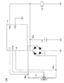
図5は、本実施の形態の通信及び給電を同時に行う給電システムのブロック図である。図5に示す給電システムは、送電装置100及び受電装置110を有している。
[Embodiment 1]
<Configuration of power supply system>
FIG. 5 is a block diagram of a power feeding system that simultaneously performs communication and power feeding according to the present embodiment. The power supply system illustrated in FIG. 5 includes a
図5に示す給電システムでは、送電装置100で発生させる電磁波に振幅変調をかけ、当該振幅変調をかけた電磁波(変調信号)を用いて送電装置100及び受電装置110間で無線通信を行う。なお、送電装置100から受電装置110へ送信される変調信号を送信信号とする。また受電装置110によって送電装置100へ反射される電波に含まれる変調信号を返信信号とする。
In the power supply system illustrated in FIG. 5, amplitude modulation is performed on the electromagnetic wave generated by the
図5に示す送電装置100は、変調回路141、復調回路142、制御回路105、方向性結合器103、第1のアンテナ151を有している。
A
図5に示す受電装置110は、第2のアンテナ152、変圧器125(トランスともいう)、整流回路115、平滑化回路116、蓄電装置120、通信制御部119を有している。
The
<送電装置の詳細な構成>
また本実施の形態の送電装置の詳細な構成を図4に示す。図4に示す送電装置100は、変調回路141、復調回路142、制御回路105、方向性結合器103、第1のアンテナ151を有している。図4に示す第1のアンテナ151は、第1の電磁結合コイル106、第1の共鳴コイル108、及び第1のコンデンサ109を有している。なお本実施の形態では、交流電源107は送電装置100の外部に設けるが、必要であれば、交流電源107を送電装置100の内部に設けてもよい。
<Detailed configuration of power transmission device>
FIG. 4 shows a detailed configuration of the power transmission device according to the present embodiment. A
本実施の形態では、交流電源107で生成された交流電力は、電磁結合により第1の電磁結合コイル106から第1の共鳴コイル108へ送電される。また、第1の共鳴コイル108と第1のコンデンサ109により、第1のLC共振回路が構成される。当該交流電力は、送電装置100の第1のLC共振回路と、後述する受電装置110の第2のLC共振回路が同一の周波数で共鳴(LC共振)することにより、送電装置100の第1のLC共振回路から受電装置110の第2のLC共振回路へ送電される。さらに、受電装置110の第2のLC共振回路が受電した交流電力は、受電装置110の第2の共鳴コイル112から後述する第2の電磁結合コイル113へ、電磁結合にて送電される。
In the present embodiment, AC power generated by
なお、送電装置100及び受電装置110間の交流電力の送電を、共鳴現象を利用せず、電磁結合を用いて行う場合は、送電装置100の第1の共鳴コイル108及び第1のコンデンサ109、並びに、受電装置110の第2の共鳴コイル112及び第2のコンデンサ111は設けなくてもよい。送電装置100及び受電装置110間の交流電力の送電を、電磁結合を用いて行う場合は、送電装置100の第1の電磁結合コイル106及び受電装置110の第2の電磁結合コイル113の電磁結合を用いて行えばよい。
Note that when the AC power transmission between the
交流電源107は高周波の交流電力を生成する電源である。交流電源107の一方の端子は、変調回路141の第1の端子に電気的に接続されている。交流電源107の他方の端子は、接地されている。
The
変調回路141は、制御回路105から出力された送信信号を、無線通信可能な信号に変換する機能を有する回路である。変調回路141の第1の端子は、交流電源107の第1の端子に電気的に接続されている。変調回路141の第2の端子は、方向性結合器103の第1の端子に電気的に接続されている。変調回路141の第3の端子は、制御回路105の第1の端子に電気的に接続されている。
The
復調回路142は、受電装置110からの無線信号(本明細書では返信信号という)を制御回路105が処理可能な信号に変換する機能を有する回路である。復調回路142の第1の端子は、方向性結合器103の第2の端子に電気的に接続されている。復調回路142の第2の端子は、制御回路105の第2の端子に電気的に接続されている。
The
制御回路105は、受電装置110へ送信する変調信号(送信信号)を生成する機能や、当該変調信号(送信信号)に応じて受電装置110から返信され、受電装置110の情報を有する変調信号(返信信号)を処理する機能を有している。制御回路105の第1の端子は、変調回路141の第3の端子に電気的に接続されている。制御回路105の第2の端子は、復調回路142の第2の端子に電気的に接続されている。
The
方向性結合器103(「カプラ」ともいう)は、順方向に伝搬する電力(進行波)若しくは逆方向に伝搬する電力(反射波)、またはその両方に対応する信号を取り出すことができる。方向性結合器103の第1の端子は、変調回路141の第2の端子に電気的に接続されている。方向性結合器103の第2の端子は、復調回路142の第1の端子に電気的に接続されている。方向性結合器103の第3の端子は、第1のアンテナ151の第1の電磁結合コイル106の一方の端子に電気的に接続されている。
The directional coupler 103 (also referred to as “coupler”) can extract a signal corresponding to power propagating in the forward direction (traveling wave), power propagating in the reverse direction (reflected wave), or both. The first terminal of the
第1の電磁結合コイル106は、上述のように、電磁結合により第1の電磁結合コイル106から第1の共鳴コイル108に交流電力を送電する機能を有する。第1の電磁結合コイル106の一方の端子は、方向性結合器103の第3の端子に電気的に接続されている。第1の電磁結合コイル106の他方の端子は、接地されている。
As described above, the first
第1のLC共振回路は、受電装置110の第2のLC共振回路と、同一の周波数で共鳴(LC共振)することにより、交流電力を送電する機能を有する。第1の共鳴コイル108の一方の端子は、第1のコンデンサ109の一方の端子に電気的に接続されている。第1の共鳴コイル108の他方の端子は、第1のコンデンサ109の他方の端子に電気的に接続されている。
The first LC resonance circuit has a function of transmitting AC power by resonating with the second LC resonance circuit of the
なお上述のように、送電装置100及び受電装置110間の交流電力の送電を、共鳴現象を利用せず、電磁結合を用いて行う場合は、送電装置100の第1の電磁結合コイル106及び受電装置110の第2の電磁結合コイル113の電磁結合を用いて行えばよく、送電装置100の第1の共鳴コイル108及び第1のコンデンサ109、並びに、受電装置110の第2の共鳴コイル112及び第2のコンデンサ111は設けなくてもよい。
As described above, when the AC power is transmitted between the
<受電装置の詳細な構成>
本実施の形態の受電装置の詳細な構成を図1に示す。図1に示す受電装置110は、第2のアンテナ152、変圧器125、整流回路115、平滑化回路116、蓄電装置120、通信制御部119を有している。図1に示す第2のアンテナ152は、第2の電磁結合コイル113、第2の共鳴コイル112、第2のコンデンサ111を有している。また通信制御部119は、リファレンス電圧生成部123、無線インターフェース部121、及び制御回路122を有している。
<Detailed configuration of power receiving device>
A detailed configuration of the power receiving device of this embodiment is illustrated in FIG. 1 includes a
第2の共鳴コイル112の一方の端子は、第2のコンデンサ111の一方の端子に電気的に接続されている。第2の共鳴コイル112の他方の端子は、第2のコンデンサ111の他方の端子に電気的に接続されている。第2の共鳴コイル112と第2のコンデンサ111により、第2のLC共振回路が構成される。
One terminal of the
第2の電磁結合コイル113の一方の端子、通信制御部119の無線インターフェース部121の端子Tx1、及び変圧器125の第1の端子は、ノードNDdに電気的に接続されている。第2の電磁結合コイル113の他方の端子、通信制御部119の無線インターフェース部121の端子Tx2、及び変圧器125の第2の端子は、ノードNDeに電気的に接続されている。第2の電磁結合コイル113の中心点は、通信制御部119の無線インターフェース部121の端子COMに電気的に接続されている。
One terminal of the second
変圧器125は、交流電力の電位の大きさを、電磁誘導を利用して変換する電力機器である。変圧器125として、本実施の形態では、一次側(入力側)と二次側(出力側)のコイルの巻数が同じであるような2つのコイルを有する変圧器を用いる。一次コイルと二次コイルの巻数が同じであれば、変圧器125の入力前後で、交流電力の電圧振幅を一定とさせ、かつ、交流電力の基準電圧を変化することが可能となる。
The
本実施の形態の変圧器125において、一次コイルの一方の端子を変圧器125の第1の端子、一次コイルの他方の端子を変圧器125の第2の端子、二次コイルの一方の端子を変圧器125の第3の端子、及び、二次コイルの他方の端子を変圧器125の第4の端子とする。
In the
整流回路115は、交流電力を直流電力に変換する交流−直流変換器(AC−DCコンバータ)として機能する。高い整流効率を得るためには、整流回路115として全波整流を用いることが好適である。図1に示す整流回路115は、4つのダイオードから構成されるブリッジ整流回路である。整流回路115の第1の端子と、変圧器125の第3の端子は、ノードNDaに電気的に接続されている。整流回路115の第2の端子と、変圧器125の第4の端子は、ノードNDbに電気的に接続されている。整流回路115の第3の端子、平滑化回路116の第1の端子、蓄電装置120の正極、通信制御部119のリファレンス電圧生成部123の端子VBatは、ノードNDcに電気的に接続されている。整流回路115の第4の端子は、接地されている。
The
ノードNDa、ノードNDb、ノードNDc、ノードNDd、及びノードNDeの電位を、それぞれ電位Va、電位Vb、電位Vc、電位Vd、及び電位Veとする。 The potentials of the node NDa, the node NDb, the node NDc, the node NDd, and the node NDe are the potential Va, the potential Vb, the potential Vc, the potential Vd, and the potential Ve, respectively.
平滑化回路116は、整流回路115から出力された直流電力を蓄え、かつ放出することにより、直流電力を平滑化する機能を有する。図1の受電装置110において、平滑化回路116としてコンデンサを用いる。平滑化回路116の第2の端子は、接地されている。なお平滑化回路116は、必要がなければ設けなくてもよい。
The smoothing
蓄電装置120は、整流回路115によって整流され、平滑化回路116によって平滑化されることによって得られた直流電力を蓄える機能を有する。蓄電装置120の負極は、接地されている。
The
通信制御部119は、送電装置100から受電装置110へ送電される交流電力に含まれる変調信号(送信信号)を解析する。通信制御部119は、入力された交流電力の電圧振幅の振幅変調を読み取ることで、変調信号を解析する。これにより、当該変調信号に含まれる送電装置の情報や指示を受電装置110が受信することができる。
The
なお、変調信号(送信信号)を含む交流電力を受信した受電装置110は、送電装置100へ反射電力を反射する。当該反射電力には、受電装置110の情報を含む変調信号(返信信号)が含まれている。当該返信信号を含む反射電力を受信し、当該返信信号を解析することにより、送電装置100は受電装置110の情報を得ることができる。これにより、送電装置100及び受電装置110間の通信が成立する。
Note that the
通信制御部119のリファレンス電圧生成部123は、得られた直流電力及び接地電位GNDから、無線インターフェース部121及び制御回路122の基準電位を生成する機能を有する。リファレンス電圧生成部123の端子VBatは、整流回路115の第3の端子、平滑化回路116の第1の端子、及び、蓄電装置120の正極に電気的に接続されている。リファレンス電圧生成部123の端子GNDは、接地されており、接地電位GNDが印加される。リファレンス電圧生成部123の端子AVDDは、無線インターフェース部121の端子AVDDに電気的に接続されている。リファレンス電圧生成部123の端子DVDDは、制御回路122の端子DVDDに電気的に接続されている。
The reference
リファレンス電圧生成部123によって当該直流電力から生成された電位AVDDが、リファレンス電圧生成部123の端子AVDD及び無線インターフェース部121の端子AVDDを介して、無線インターフェース部121に供給される。電位AVDD及び接地電位GNDは、無線インターフェース部121の基準電位として機能する。またリファレンス電圧生成部123によって当該直流電力から生成された電位DVDDが、リファレンス電圧生成部123の端子DVDD及び制御回路122の端子DVDDを介して、制御回路122に供給される。電位DVDD及び接地電位GNDは、制御回路122の基準電位として機能する。
The potential AVDD generated from the DC power by the reference
無線インターフェース部121は、送電装置100からの変調信号(送信信号)を制御回路122が処理可能な信号に変換する復調回路、及び、制御回路122から出力された変調信号(返信信号)を、無線通信可能な信号に変換する変調回路を有する回路である。無線インターフェース部121の端子AVDDは、リファレンス電圧生成部123の端子AVDDに電気的に接続されている。無線インターフェース部121の端子COMは、第2の電磁結合コイル113の中心点に電気的に接続されている。無線インターフェース部121の端子GNDには、接地電位GNDが印加される。無線インターフェース部121の端子CNTは、制御回路122の端子CNTに電気的に接続されている。
The
制御回路122は、受電装置110の情報を有する変調信号(返信信号)を生成する機能や、送電装置100から送信された変調信号(送信信号)を処理する機能を有している。制御回路122の端子DVDDは、リファレンス電圧生成部123の端子DVDDに電気的に接続されている。制御回路122の端子GNDは接地されており、接地電位GNDが印加される。制御回路122の端子CNTは、無線インターフェース部121の端子CNTに電気的に接続されている。
The
第2の電磁結合コイル113及び整流回路115との間に変圧器125を設けた場合の交流電力の変化を図2(C)に示す。
FIG. 2C shows a change in AC power when the
図2(C)において、通信制御部119に入力され、変調信号(送信信号)を含む交流電力を交流電力Tとし、整流回路115によって整流され直流電力に変換される交流電力を交流電力Cとする。交流電力Tの最大電位及び最小電位は、それぞれ電位Ve及び電位Vfである。また交流電力Tの中間電位を電位Vm2とする。また交流電力Cの最大電位及び最小電位は、それぞれ電位Va及び電位Vbである。また交流電力Cの中間電位を電位Vmとする。
2C, AC power input to the
第2の電磁結合コイル113及び整流回路115との間に変圧器125を設けることにより、交流電力T及び交流電力Cを互いに独立させることができる。より具体的には、交流電力Tの電圧振幅を有し、交流電力Tとは異なる中間電位を有する交流電力Cを整流回路115に供給することができる。なお、交流電力Tと交流電力Cの中間電位が同じ場合もありうる。
By providing the
別言すれば、変圧器125を設けることにより、交流電力Tの電位Vm2を電位Vmに変化させて整流回路115に入力することができる。よって、電位変動が少なく、安定した電位Vcを通信制御部119に供給することができる。
In other words, by providing the
蓄電装置120の充電に用いる直流電力は、中間電位が電位Vmの交流電力(交流電力C)から生成される。一方、通信制御部119に入力される交流電力は、中間電位が電位Vm2である交流電力Tである。交流電力Tに含まれる変調信号(送信信号)は、無線インターフェース部121によって、制御回路122が処理可能な信号に変換される。
The DC power used for charging
以上により、通信と給電を同時に行っても、通信のための交流電力T及び給電のための交流電力Cが互いに干渉せず、通信を安定に行うことが可能となる。 As described above, even when communication and power supply are performed simultaneously, the AC power T for communication and the AC power C for power supply do not interfere with each other, and communication can be performed stably.
第2の電磁結合コイル113及び整流回路115との間に変圧器125を設けた受電装置と設けない受電装置について、通信制御部119の基準電位である電位VBatの変化を図6に示す。図6においては、給電と同時に通信を行う測定を4回行った。また、図6の横軸は測定回数、縦軸は電位VBatの値である。
FIG. 6 shows a change in the potential Vbat that is the reference potential of the
また図6において、変圧器125を設けた場合と設けない場合いずれにおいても、受電電力の電力値は1.8W以上2.5W以下であった。
In FIG. 6, the power value of the received power was 1.8 W or more and 2.5 W or less with or without the
図6に示されるように、変圧器125を設けた受電装置では、電位VBatは一定の値(3.3V)を維持している。一方、変圧器125を設けない受電装置では、電位VBatは、一定の値を取らず、変動する。
As shown in FIG. 6, in the power receiving device provided with the
電位VBatが変動するということは、直流電力に変換される前の交流電力の基準電位(図2(A)に示す電位Vm)が変動しているということである。基準電位が変動する交流電力を通信に用いると、通信が不安定なる、さらには、通信が成立しなくなるという恐れがある。 The change in the potential Vbat means that the reference potential (the potential Vm shown in FIG. 2A) of the AC power before being converted into the DC power is changed. If AC power with a varying reference potential is used for communication, communication may become unstable and communication may not be established.
一方、電位VBatが一定の値を維持しているということは、給電に用いられる交流電力(図2(C)に示す交流電力C)の基準電位が一定の値で安定しているということである。変圧器を設けたことにより、給電用の交流電力(交流電力C)及び通信用の交流電力(交流電力T)が分離され、安定な通信が可能となる。 On the other hand, the fact that the potential Vbat maintains a constant value means that the reference potential of the AC power (AC power C shown in FIG. 2C) used for feeding is stable at a constant value. is there. By providing the transformer, AC power for power supply (AC power C) and AC power for communication (AC power T) are separated, and stable communication is possible.
以上説明したように、本実施の形態により、通信及び給電を同時に行うことが可能な受電装置及び給電システムを提供することができる。 As described above, according to this embodiment, it is possible to provide a power receiving device and a power feeding system that can perform communication and power feeding at the same time.
また本実施の形態により、給電中も安定な通信が行える受電装置及び給電システムを提供することができる。 Further, according to this embodiment, it is possible to provide a power receiving device and a power feeding system that can perform stable communication during power feeding.
[実施の形態2]
本実施の形態では、実施の形態1で説明した給電システムを適用できる電気機器について説明する。なお、本発明の一態様に係る給電システムを適用できる電気機器としては、携帯型の電子機器である、デジタルビデオカメラ、携帯情報端末(モバイルコンピュータ、携帯電話、携帯型ゲーム機又は電子書籍等)、記録媒体を備えた画像再生装置(具体的にはDigital Versatile Disc(DVD)再生装置)などが挙げられる。また、電力を基に動力を得る電気自動車等の電気推進移動体が挙げられる。以下、一例について図7を参照して説明する。
[Embodiment 2]
In this embodiment, electric devices to which the power feeding system described in
図7(A)は、携帯電話及び携帯情報端末を給電システムの用途とする一例であり、送電装置701、受電装置703Aを有する携帯電話702A、受電装置703Bを有する携帯電話702Bによって構成されている。実施の形態1で説明した給電システムは、送電装置701と受電装置703A及び受電装置703Bの間で適用することができる。
FIG. 7A illustrates an example in which a cellular phone and a portable information terminal are used for a power feeding system. The cellular phone and a portable information terminal include a
図7(B)は、電気推進移動体である電気自動車を給電システムの用途とする一例であり、送電装置711と、受電装置713を有する電気自動車712とによって構成されている。実施の形態1で説明した給電システムは、送電装置711と受電装置713の間で適用することができる。
FIG. 7B illustrates an example in which an electric vehicle that is an electric propulsion moving body is used as a power supply system. The electric vehicle includes a
以上説明したように、本実施の形態により、通信及び給電を同時に行うことが可能な受電装置及び給電システムを提供することができる。 As described above, according to this embodiment, it is possible to provide a power receiving device and a power feeding system that can perform communication and power feeding at the same time.
また本実施の形態により、給電中も安定な通信が行える受電装置及び給電システムを提供することができる。 Further, according to this embodiment, it is possible to provide a power receiving device and a power feeding system that can perform stable communication during power feeding.
本実施の形態により、電気機器に対して安定な給電及び通信を同時に行うことが可能である。 According to this embodiment mode, stable power feeding and communication can be performed simultaneously with respect to an electric device.
100 送電装置
103 方向性結合器
105 制御回路
106 第1の電磁結合コイル
107 交流電源
108 第1の共鳴コイル
109 第1のコンデンサ
110 受電装置
111 第2のコンデンサ
112 第2の共鳴コイル
113 第2の電磁結合コイル
115 整流回路
116 平滑化回路
119 通信制御部
120 蓄電装置
121 無線インターフェース部
122 制御回路
123 リファレンス電圧生成部
125 変圧器
130 受電装置
151 第1のアンテナ
152 第2のアンテナ
701 送電装置
702A 携帯電話
702B 携帯電話
703A 受電装置
703B 受電装置
711 送電装置
712 電気自動車
713 受電装置
100
Claims (4)
受信した前記変調信号を含む前記交流電力を整流することにより、前記変調信号を含む前記交流電力を直流電力に変換する整流回路と、
前記直流電力を平滑化する平滑化回路と、
平滑化された前記直流電力を蓄える蓄電装置と、
前記変調信号を含む前記交流電力が入力され、前記変調信号を解析し、前記直流電力の電位及び接地電位を用いて駆動される通信制御部と、
前記通信用及び給電用アンテナと前記整流回路との間に配置され、前記通信制御部に入力される前記交流電力における第1の電位を変化させる変圧器と、を有し、
前記第1の電位は、前記交流電力の最大電位と最小電位の中間の電位であり、
前記通信用及び給電用アンテナは、前記変調信号を含む前記交流電力を受信するのと同時に、前記変調信号を含む前記交流電力を送信した装置に反射電力を送信する、ことを特徴とする受電装置。 An antenna for communication and feeding that receives AC power including a modulation signal;
A rectifying circuit that converts the AC power including the modulation signal into DC power by rectifying the AC power including the received modulation signal;
A smoothing circuit for smoothing the DC power;
A power storage device for storing the smoothed DC power;
A communication control unit that receives the AC power including the modulation signal, analyzes the modulation signal, and is driven using a potential of the DC power and a ground potential;
A transformer that is arranged between the communication and feeding antennas and the rectifier circuit and changes a first potential in the AC power input to the communication control unit;
The first potential is an intermediate potential between the maximum potential and the minimum potential of the AC power,
The power receiving device, wherein the communication antenna and the power feeding antenna transmit reflected power to a device that has transmitted the AC power including the modulation signal simultaneously with receiving the AC power including the modulation signal. .
前記通信制御部は、
前記変調信号を解析する制御回路と、
前記変調信号を前記制御回路が解析可能な信号に変換する無線インターフェース部と、
前記直流電力の電位及び前記接地電位を用いて、前記制御回路及び前記無線インターフェース部へ供給する電位を生成するリファレンス電圧生成部と、を有し、
前記無線インターフェース部は、
前記通信用及び給電用アンテナの一方の端子、前記通信用及び給電用アンテナの中心点、前記通信用及び給電用アンテナの他方の端子、前記リファレンス電圧生成部及び前記制御回路と、接続し、
前記無線インターフェース部の端子の一つは接地され、
前記リファレンス電圧生成部は、前記接地電位及び前記直流電力が入力され、前記無線インターフェース部及び前記制御回路と接続する、ことを特徴とする受電装置。 In claim 1,
The communication control unit
A control circuit for analyzing the modulated signal;
A wireless interface unit that converts the modulated signal into a signal that can be analyzed by the control circuit;
A reference voltage generation unit that generates a potential to be supplied to the control circuit and the wireless interface unit using the potential of the DC power and the ground potential;
The wireless interface unit is
Connecting one terminal of the communication and power feeding antenna, a central point of the communication and power feeding antenna, the other terminal of the communication and power feeding antenna, the reference voltage generation unit, and the control circuit;
One of the terminals of the wireless interface unit is grounded,
The power receiving device, wherein the reference voltage generation unit receives the ground potential and the DC power and is connected to the wireless interface unit and the control circuit.
送信装置は、
第1の変調信号を生成する第1の制御回路と、
前記第1の変調信号を無線通信可能な信号に変換する変調回路と、
前記第1の変調信号を含む第1の交流電力を送信する第1のアンテナと、を有し、
受電装置は、
前記第1の変調信号を含む前記第1の交流電力を受信する、通信用及び給電用の第2のアンテナと、
前記第2のアンテナが受信した前記第1の変調信号を含む前記第1の交流電力を整流することにより、前記第1の変調信号を含む前記第1の交流電力を直流電力に変換する整流回路と、
前記直流電力を平滑化する平滑化回路と、
平滑化された前記直流電力を蓄える蓄電装置と、
前記第1の変調信号を含む前記第1の交流電力が入力され、前記第1の変調信号を解析し、前記直流電力の電位及び接地電位を用いて駆動される通信制御部と、
前記第2のアンテナと前記整流回路との間に配置され、前記通信制御部に入力される前記第1の交流電力における第1の電位を変化させる変圧器と、を有し、
前記第1の電位は、前記第1の交流電力の最大電位と最小電位の中間の電位であり、
前記送信装置から前記受電装置へ前記第1の変調信号を含む前記第1の交流電力を送信するのと同時に、前記受電装置から前記送信装置へ第2の変調信号を含む第2の交流電力を送信し、
前記第2の変調信号は、前記受電装置の情報を含むことを特徴とする、給電システム。 A transmitting device and a power receiving device;
The transmitter is
A first control circuit for generating a first modulated signal;
A modulation circuit for converting the first modulated signal into a signal capable of wireless communication;
A first antenna for transmitting a first AC power including the first modulated signal,
The power receiving device
A second antenna for communication and feeding that receives the first AC power including the first modulated signal;
A rectifier circuit that converts the first AC power including the first modulation signal into DC power by rectifying the first AC power including the first modulation signal received by the second antenna. When,
A smoothing circuit for smoothing the DC power;
A power storage device for storing the smoothed DC power;
A communication control unit that receives the first AC power including the first modulation signal, analyzes the first modulation signal, and is driven using the potential of the DC power and a ground potential;
A transformer that is disposed between the second antenna and the rectifier circuit and changes a first potential in the first AC power input to the communication control unit;
The first potential is an intermediate potential between the maximum potential and the minimum potential of the first AC power,
The same time from the transmission device and for transmitting the first AC power including the first modulated signal to the power receiving device, the second AC power including a second modulated signal to the transmitting apparatus from the power receiving device Send
The power supply system, wherein the second modulation signal includes information of the power receiving device.
前記通信制御部は、
前記第1の変調信号を解析する第2の制御回路と、
前記第1の変調信号を前記第2の制御回路が解析可能な信号に変換する無線インターフェース部と、
前記直流電力の電位及び前記接地電位から、前記第2の制御回路及び前記無線インターフェース部へ供給される電位を生成するリファレンス電圧生成部と、を有し、
前記無線インターフェース部は、
前記通信用及び給電用アンテナの一方の端子、前記通信用及び給電用アンテナの中心点、前記通信用及び給電用アンテナの他方の端子、前記リファレンス電圧生成部及び前記第2の制御回路と、接続し、
前記無線インターフェース部の端子の一つは接地され、
前記リファレンス電圧生成部は、前記接地電位及び前記直流電力が入力され、前記無線インターフェース部及び前記第2の制御回路と接続する、ことを特徴とする給電システム。 In claim 3,
The communication control unit
A second control circuit for analyzing the first modulated signal;
A wireless interface unit that converts the first modulated signal into a signal that can be analyzed by the second control circuit;
A reference voltage generation unit that generates a potential supplied to the second control circuit and the wireless interface unit from the potential of the DC power and the ground potential;
The wireless interface unit is
Connection with one terminal of the communication and power supply antenna, a center point of the communication and power supply antenna, the other terminal of the communication and power supply antenna, the reference voltage generation unit, and the second control circuit And
One of the terminals of the wireless interface unit is grounded,
The power supply system, wherein the reference voltage generation unit receives the ground potential and the DC power and is connected to the wireless interface unit and the second control circuit.
Priority Applications (1)
| Application Number | Priority Date | Filing Date | Title |
|---|---|---|---|
| JP2013061580A JP6305686B2 (en) | 2012-03-26 | 2013-03-25 | Power receiving device and power feeding system |
Applications Claiming Priority (3)
| Application Number | Priority Date | Filing Date | Title |
|---|---|---|---|
| JP2012069626 | 2012-03-26 | ||
| JP2012069626 | 2012-03-26 | ||
| JP2013061580A JP6305686B2 (en) | 2012-03-26 | 2013-03-25 | Power receiving device and power feeding system |
Related Child Applications (1)
| Application Number | Title | Priority Date | Filing Date |
|---|---|---|---|
| JP2018040754A Division JP6585210B2 (en) | 2012-03-26 | 2018-03-07 | Power receiving device |
Publications (3)
| Publication Number | Publication Date |
|---|---|
| JP2013230079A JP2013230079A (en) | 2013-11-07 |
| JP2013230079A5 JP2013230079A5 (en) | 2016-03-10 |
| JP6305686B2 true JP6305686B2 (en) | 2018-04-04 |
Family
ID=49211121
Family Applications (3)
| Application Number | Title | Priority Date | Filing Date |
|---|---|---|---|
| JP2013061580A Active JP6305686B2 (en) | 2012-03-26 | 2013-03-25 | Power receiving device and power feeding system |
| JP2018040754A Active JP6585210B2 (en) | 2012-03-26 | 2018-03-07 | Power receiving device |
| JP2019161230A Active JP6768902B2 (en) | 2012-03-26 | 2019-09-04 | Power receiving device |
Family Applications After (2)
| Application Number | Title | Priority Date | Filing Date |
|---|---|---|---|
| JP2018040754A Active JP6585210B2 (en) | 2012-03-26 | 2018-03-07 | Power receiving device |
| JP2019161230A Active JP6768902B2 (en) | 2012-03-26 | 2019-09-04 | Power receiving device |
Country Status (2)
| Country | Link |
|---|---|
| US (2) | US9641223B2 (en) |
| JP (3) | JP6305686B2 (en) |
Families Citing this family (7)
| Publication number | Priority date | Publication date | Assignee | Title |
|---|---|---|---|---|
| US9847675B2 (en) | 2011-12-16 | 2017-12-19 | Semiconductor Energy Laboratory Co., Ltd. | Power receiving device and power feeding system |
| CN205304411U (en) * | 2013-06-05 | 2016-06-08 | 株式会社村田制作所 | Electron device and wireless electric power transmission system |
| WO2015118945A1 (en) | 2014-02-07 | 2015-08-13 | 株式会社村田製作所 | Power transmission system |
| CN106663528B (en) * | 2014-07-09 | 2020-05-05 | 奥克兰联合服务有限公司 | Inductive power system suitable for electric vehicle |
| JP6446194B2 (en) | 2014-07-17 | 2018-12-26 | ローム株式会社 | Wireless power receiving apparatus, receiver circuit thereof, and method for controlling wireless power receiving apparatus |
| JP6785846B2 (en) * | 2016-04-26 | 2020-11-18 | 三菱電機株式会社 | Elevator electrical safety device |
| RU2669141C1 (en) * | 2017-06-22 | 2018-10-08 | Акционерное общество "Омский научно-исследовательский институт приборостроения" (АО "ОНИИП") | Key radio transmitter |
Family Cites Families (36)
| Publication number | Priority date | Publication date | Assignee | Title |
|---|---|---|---|---|
| US6611199B1 (en) * | 1995-10-11 | 2003-08-26 | Motorola, Inc. | Capacitively powered portable communication device and associated exciter/reader and related method |
| JP4200257B2 (en) | 2000-09-26 | 2008-12-24 | パナソニック電工株式会社 | Non-contact power transmission device |
| US6665527B2 (en) * | 2000-11-30 | 2003-12-16 | Motorola, Inc. | Double balanced mixer circuit |
| JP2002209375A (en) * | 2001-01-10 | 2002-07-26 | Seiko Epson Corp | Voltage conversion circuit |
| JP2006180073A (en) | 2004-12-21 | 2006-07-06 | Okayama Prefecture | Wireless ic tag |
| US7449105B2 (en) | 2006-07-19 | 2008-11-11 | Denny Hastings Flp 14 | Water filtration and erosion control system |
| JP4494426B2 (en) * | 2007-02-16 | 2010-06-30 | セイコーエプソン株式会社 | Power transmission control device, power reception control device, non-contact power transmission system, power transmission device, power reception device, and electronic equipment |
| CN100576711C (en) * | 2007-03-29 | 2009-12-30 | 雅米科技股份有限公司 | Induction power system |
| JP4743173B2 (en) | 2007-06-29 | 2011-08-10 | セイコーエプソン株式会社 | Power transmission control device, power transmission device, non-contact power transmission system, and electronic device |
| JP2010539887A (en) * | 2007-09-19 | 2010-12-16 | クゥアルコム・インコーポレイテッド | Maximizing the power generated from wireless power magnetic resonators |
| JP5556002B2 (en) | 2008-01-09 | 2014-07-23 | セイコーエプソン株式会社 | Power transmission control device, power transmission device, non-contact power transmission system, and electronic device |
| JP2009240099A (en) | 2008-03-27 | 2009-10-15 | Dainippon Printing Co Ltd | Non-contact power feeding device, power feeder and power receiver |
| JP4561886B2 (en) * | 2008-06-27 | 2010-10-13 | ソニー株式会社 | Power transmission device, power feeding device, and power receiving device |
| US8299652B2 (en) * | 2008-08-20 | 2012-10-30 | Intel Corporation | Wireless power transfer apparatus and method thereof |
| JP5258521B2 (en) | 2008-11-14 | 2013-08-07 | トヨタ自動車株式会社 | Power supply system |
| JP2010193598A (en) | 2009-02-17 | 2010-09-02 | Nippon Soken Inc | Noncontact power supply facility and noncontact power supply system |
| JP5621203B2 (en) | 2009-03-30 | 2014-11-12 | 富士通株式会社 | Wireless power supply system and wireless power supply method |
| JP2010252468A (en) | 2009-04-14 | 2010-11-04 | Sony Corp | Power transmission device and method, power receiving device and method, and power transmission system |
| KR20120023765A (en) | 2009-05-14 | 2012-03-13 | 도요타 지도샤(주) | Vehicle charging unit |
| JP5431033B2 (en) | 2009-06-08 | 2014-03-05 | Necトーキン株式会社 | Contactless power transmission and communication system |
| JP2010284066A (en) | 2009-06-08 | 2010-12-16 | Nec Tokin Corp | Communication device, communication terminal and communication system |
| JP2011029799A (en) | 2009-07-23 | 2011-02-10 | Sony Corp | Contactless power supplying communication apparatus, contactless power receiving communication device, power-supplying communication control method, and power receiving communication control method |
| JP2011061893A (en) | 2009-09-07 | 2011-03-24 | Seiko Epson Corp | Power transmission and reception control unit, power transmitting and receiving apparatus, electronic apparatus and control method |
| JP5454781B2 (en) | 2010-01-15 | 2014-03-26 | 株式会社ダイフク | Lead-acid battery charger |
| JP5526833B2 (en) | 2010-02-05 | 2014-06-18 | ソニー株式会社 | Wireless power transmission device |
| JP5476194B2 (en) | 2010-04-08 | 2014-04-23 | Necトーキン株式会社 | Non-contact power transmission and communication system, power transmission device and power reception device |
| US9561730B2 (en) * | 2010-04-08 | 2017-02-07 | Qualcomm Incorporated | Wireless power transmission in electric vehicles |
| JP2012005185A (en) | 2010-06-14 | 2012-01-05 | Nec Tokin Corp | Non-contact power transmission and communication system |
| JP5395018B2 (en) | 2010-09-07 | 2014-01-22 | 日本電信電話株式会社 | Resonant type wireless power transmission device |
| JP5456625B2 (en) | 2010-09-07 | 2014-04-02 | 日本電信電話株式会社 | Resonant type wireless power transmission device |
| US20120223593A1 (en) * | 2011-03-03 | 2012-09-06 | Semiconductor Energy Laboratory Co., Ltd. | Power receiving device and wireless power supply system |
| JP5780894B2 (en) | 2011-09-16 | 2015-09-16 | 株式会社半導体エネルギー研究所 | Contactless power supply system |
| US9847675B2 (en) | 2011-12-16 | 2017-12-19 | Semiconductor Energy Laboratory Co., Ltd. | Power receiving device and power feeding system |
| TWI613882B (en) | 2011-12-16 | 2018-02-01 | 半導體能源研究所股份有限公司 | Dc-dc converter, power receiving device, and power feeding system |
| US9673867B2 (en) | 2012-03-14 | 2017-06-06 | Semiconductor Energy Laboratory Co., Ltd. | Power transmission device and power feeding system |
| US8933662B2 (en) * | 2012-07-26 | 2015-01-13 | Daifuku Co., Ltd. | Charging apparatus for lead storage battery |
-
2013
- 2013-03-14 US US13/804,883 patent/US9641223B2/en active Active
- 2013-03-25 JP JP2013061580A patent/JP6305686B2/en active Active
-
2017
- 2017-05-01 US US15/583,446 patent/US10615849B2/en active Active
-
2018
- 2018-03-07 JP JP2018040754A patent/JP6585210B2/en active Active
-
2019
- 2019-09-04 JP JP2019161230A patent/JP6768902B2/en active Active
Also Published As
| Publication number | Publication date |
|---|---|
| JP6585210B2 (en) | 2019-10-02 |
| JP2018113856A (en) | 2018-07-19 |
| US10615849B2 (en) | 2020-04-07 |
| US20170237470A1 (en) | 2017-08-17 |
| JP2013230079A (en) | 2013-11-07 |
| US20130249309A1 (en) | 2013-09-26 |
| JP2020005499A (en) | 2020-01-09 |
| JP6768902B2 (en) | 2020-10-14 |
| US9641223B2 (en) | 2017-05-02 |
Similar Documents
| Publication | Publication Date | Title |
|---|---|---|
| JP6585210B2 (en) | Power receiving device | |
| JP5780894B2 (en) | Contactless power supply system | |
| US10340739B2 (en) | Power receiving device, power transmission device, and power feeding system | |
| JP5947534B2 (en) | Contactless power supply system | |
| JP6266207B2 (en) | Power receiving device | |
| US20150311744A1 (en) | Wireless power feeding system | |
| US20130015813A1 (en) | Wireless power receiver | |
| JP2020120580A (en) | Operation method for power feeding system | |
| JP2012165633A (en) | Power supply device and noncontact power supply system | |
| JP5960438B2 (en) | Power supply system and power supply method | |
| KR102452017B1 (en) | Apparatus for transmitting and receiving wireless power | |
| US9673867B2 (en) | Power transmission device and power feeding system | |
| JP2010284066A (en) | Communication device, communication terminal and communication system | |
| US11171518B2 (en) | Wireless power system with reconfigurable rectifier circuitry | |
| CN111799891B (en) | Wireless power system with reconfigurable rectifier circuit | |
| KR20100088119A (en) | Portable terminal |
Legal Events
| Date | Code | Title | Description |
|---|---|---|---|
| A521 | Request for written amendment filed |
Free format text: JAPANESE INTERMEDIATE CODE: A523 Effective date: 20160122 |
|
| A621 | Written request for application examination |
Free format text: JAPANESE INTERMEDIATE CODE: A621 Effective date: 20160122 |
|
| A977 | Report on retrieval |
Free format text: JAPANESE INTERMEDIATE CODE: A971007 Effective date: 20160929 |
|
| A131 | Notification of reasons for refusal |
Free format text: JAPANESE INTERMEDIATE CODE: A131 Effective date: 20161101 |
|
| A521 | Request for written amendment filed |
Free format text: JAPANESE INTERMEDIATE CODE: A523 Effective date: 20161226 |
|
| A131 | Notification of reasons for refusal |
Free format text: JAPANESE INTERMEDIATE CODE: A131 Effective date: 20170606 |
|
| A521 | Request for written amendment filed |
Free format text: JAPANESE INTERMEDIATE CODE: A523 Effective date: 20170802 |
|
| TRDD | Decision of grant or rejection written | ||
| A01 | Written decision to grant a patent or to grant a registration (utility model) |
Free format text: JAPANESE INTERMEDIATE CODE: A01 Effective date: 20180206 |
|
| A61 | First payment of annual fees (during grant procedure) |
Free format text: JAPANESE INTERMEDIATE CODE: A61 Effective date: 20180307 |
|
| R150 | Certificate of patent or registration of utility model |
Ref document number: 6305686 Country of ref document: JP Free format text: JAPANESE INTERMEDIATE CODE: R150 |
|
| R250 | Receipt of annual fees |
Free format text: JAPANESE INTERMEDIATE CODE: R250 |
|
| R250 | Receipt of annual fees |
Free format text: JAPANESE INTERMEDIATE CODE: R250 |
|
| R250 | Receipt of annual fees |
Free format text: JAPANESE INTERMEDIATE CODE: R250 |