JP6300349B2 - Circuit including switching element, rectifier element, and charge storage element - Google Patents
Circuit including switching element, rectifier element, and charge storage element Download PDFInfo
- Publication number
- JP6300349B2 JP6300349B2 JP2014021259A JP2014021259A JP6300349B2 JP 6300349 B2 JP6300349 B2 JP 6300349B2 JP 2014021259 A JP2014021259 A JP 2014021259A JP 2014021259 A JP2014021259 A JP 2014021259A JP 6300349 B2 JP6300349 B2 JP 6300349B2
- Authority
- JP
- Japan
- Prior art keywords
- terminal
- charge storage
- circuit
- side transistor
- capacitor
- Prior art date
- Legal status (The legal status is an assumption and is not a legal conclusion. Google has not performed a legal analysis and makes no representation as to the accuracy of the status listed.)
- Active
Links
- 239000003990 capacitor Substances 0.000 claims description 99
- 230000003071 parasitic effect Effects 0.000 claims description 56
- 230000015556 catabolic process Effects 0.000 description 39
- 230000005669 field effect Effects 0.000 description 9
- 238000010586 diagram Methods 0.000 description 8
- 230000008901 benefit Effects 0.000 description 6
- 238000000034 method Methods 0.000 description 4
- 230000008878 coupling Effects 0.000 description 2
- 238000010168 coupling process Methods 0.000 description 2
- 238000005859 coupling reaction Methods 0.000 description 2
- 239000000463 material Substances 0.000 description 2
- 230000002411 adverse Effects 0.000 description 1
- 230000008859 change Effects 0.000 description 1
- 230000000694 effects Effects 0.000 description 1
- 238000005516 engineering process Methods 0.000 description 1
- 230000006870 function Effects 0.000 description 1
- 238000002955 isolation Methods 0.000 description 1
- 230000015654 memory Effects 0.000 description 1
- 239000002184 metal Substances 0.000 description 1
- 230000003287 optical effect Effects 0.000 description 1
- 239000004065 semiconductor Substances 0.000 description 1
- 230000001052 transient effect Effects 0.000 description 1
Images


Classifications
-
- H—ELECTRICITY
- H01—ELECTRIC ELEMENTS
- H01L—SEMICONDUCTOR DEVICES NOT COVERED BY CLASS H10
- H01L27/00—Devices consisting of a plurality of semiconductor or other solid-state components formed in or on a common substrate
- H01L27/02—Devices consisting of a plurality of semiconductor or other solid-state components formed in or on a common substrate including semiconductor components specially adapted for rectifying, oscillating, amplifying or switching and having at least one potential-jump barrier or surface barrier; including integrated passive circuit elements with at least one potential-jump barrier or surface barrier
- H01L27/04—Devices consisting of a plurality of semiconductor or other solid-state components formed in or on a common substrate including semiconductor components specially adapted for rectifying, oscillating, amplifying or switching and having at least one potential-jump barrier or surface barrier; including integrated passive circuit elements with at least one potential-jump barrier or surface barrier the substrate being a semiconductor body
- H01L27/06—Devices consisting of a plurality of semiconductor or other solid-state components formed in or on a common substrate including semiconductor components specially adapted for rectifying, oscillating, amplifying or switching and having at least one potential-jump barrier or surface barrier; including integrated passive circuit elements with at least one potential-jump barrier or surface barrier the substrate being a semiconductor body including a plurality of individual components in a non-repetitive configuration
- H01L27/0611—Devices consisting of a plurality of semiconductor or other solid-state components formed in or on a common substrate including semiconductor components specially adapted for rectifying, oscillating, amplifying or switching and having at least one potential-jump barrier or surface barrier; including integrated passive circuit elements with at least one potential-jump barrier or surface barrier the substrate being a semiconductor body including a plurality of individual components in a non-repetitive configuration integrated circuits having a two-dimensional layout of components without a common active region
- H01L27/0617—Devices consisting of a plurality of semiconductor or other solid-state components formed in or on a common substrate including semiconductor components specially adapted for rectifying, oscillating, amplifying or switching and having at least one potential-jump barrier or surface barrier; including integrated passive circuit elements with at least one potential-jump barrier or surface barrier the substrate being a semiconductor body including a plurality of individual components in a non-repetitive configuration integrated circuits having a two-dimensional layout of components without a common active region comprising components of the field-effect type
- H01L27/0629—Devices consisting of a plurality of semiconductor or other solid-state components formed in or on a common substrate including semiconductor components specially adapted for rectifying, oscillating, amplifying or switching and having at least one potential-jump barrier or surface barrier; including integrated passive circuit elements with at least one potential-jump barrier or surface barrier the substrate being a semiconductor body including a plurality of individual components in a non-repetitive configuration integrated circuits having a two-dimensional layout of components without a common active region comprising components of the field-effect type in combination with diodes, or resistors, or capacitors
-
- H—ELECTRICITY
- H03—ELECTRONIC CIRCUITRY
- H03K—PULSE TECHNIQUE
- H03K17/00—Electronic switching or gating, i.e. not by contact-making and –breaking
- H03K17/08—Modifications for protecting switching circuit against overcurrent or overvoltage
- H03K17/081—Modifications for protecting switching circuit against overcurrent or overvoltage without feedback from the output circuit to the control circuit
- H03K17/0814—Modifications for protecting switching circuit against overcurrent or overvoltage without feedback from the output circuit to the control circuit by measures taken in the output circuit
-
- H—ELECTRICITY
- H02—GENERATION; CONVERSION OR DISTRIBUTION OF ELECTRIC POWER
- H02M—APPARATUS FOR CONVERSION BETWEEN AC AND AC, BETWEEN AC AND DC, OR BETWEEN DC AND DC, AND FOR USE WITH MAINS OR SIMILAR POWER SUPPLY SYSTEMS; CONVERSION OF DC OR AC INPUT POWER INTO SURGE OUTPUT POWER; CONTROL OR REGULATION THEREOF
- H02M1/00—Details of apparatus for conversion
- H02M1/32—Means for protecting converters other than automatic disconnection
-
- H—ELECTRICITY
- H02—GENERATION; CONVERSION OR DISTRIBUTION OF ELECTRIC POWER
- H02M—APPARATUS FOR CONVERSION BETWEEN AC AND AC, BETWEEN AC AND DC, OR BETWEEN DC AND DC, AND FOR USE WITH MAINS OR SIMILAR POWER SUPPLY SYSTEMS; CONVERSION OF DC OR AC INPUT POWER INTO SURGE OUTPUT POWER; CONTROL OR REGULATION THEREOF
- H02M3/00—Conversion of dc power input into dc power output
- H02M3/02—Conversion of dc power input into dc power output without intermediate conversion into ac
- H02M3/04—Conversion of dc power input into dc power output without intermediate conversion into ac by static converters
- H02M3/10—Conversion of dc power input into dc power output without intermediate conversion into ac by static converters using discharge tubes with control electrode or semiconductor devices with control electrode
- H02M3/145—Conversion of dc power input into dc power output without intermediate conversion into ac by static converters using discharge tubes with control electrode or semiconductor devices with control electrode using devices of a triode or transistor type requiring continuous application of a control signal
- H02M3/155—Conversion of dc power input into dc power output without intermediate conversion into ac by static converters using discharge tubes with control electrode or semiconductor devices with control electrode using devices of a triode or transistor type requiring continuous application of a control signal using semiconductor devices only
- H02M3/156—Conversion of dc power input into dc power output without intermediate conversion into ac by static converters using discharge tubes with control electrode or semiconductor devices with control electrode using devices of a triode or transistor type requiring continuous application of a control signal using semiconductor devices only with automatic control of output voltage or current, e.g. switching regulators
- H02M3/158—Conversion of dc power input into dc power output without intermediate conversion into ac by static converters using discharge tubes with control electrode or semiconductor devices with control electrode using devices of a triode or transistor type requiring continuous application of a control signal using semiconductor devices only with automatic control of output voltage or current, e.g. switching regulators including plural semiconductor devices as final control devices for a single load
- H02M3/1588—Conversion of dc power input into dc power output without intermediate conversion into ac by static converters using discharge tubes with control electrode or semiconductor devices with control electrode using devices of a triode or transistor type requiring continuous application of a control signal using semiconductor devices only with automatic control of output voltage or current, e.g. switching regulators including plural semiconductor devices as final control devices for a single load comprising at least one synchronous rectifier element
-
- H—ELECTRICITY
- H02—GENERATION; CONVERSION OR DISTRIBUTION OF ELECTRIC POWER
- H02M—APPARATUS FOR CONVERSION BETWEEN AC AND AC, BETWEEN AC AND DC, OR BETWEEN DC AND DC, AND FOR USE WITH MAINS OR SIMILAR POWER SUPPLY SYSTEMS; CONVERSION OF DC OR AC INPUT POWER INTO SURGE OUTPUT POWER; CONTROL OR REGULATION THEREOF
- H02M7/00—Conversion of ac power input into dc power output; Conversion of dc power input into ac power output
- H02M7/42—Conversion of dc power input into ac power output without possibility of reversal
- H02M7/44—Conversion of dc power input into ac power output without possibility of reversal by static converters
- H02M7/48—Conversion of dc power input into ac power output without possibility of reversal by static converters using discharge tubes with control electrode or semiconductor devices with control electrode
- H02M7/53—Conversion of dc power input into ac power output without possibility of reversal by static converters using discharge tubes with control electrode or semiconductor devices with control electrode using devices of a triode or transistor type requiring continuous application of a control signal
- H02M7/537—Conversion of dc power input into ac power output without possibility of reversal by static converters using discharge tubes with control electrode or semiconductor devices with control electrode using devices of a triode or transistor type requiring continuous application of a control signal using semiconductor devices only, e.g. single switched pulse inverters
- H02M7/538—Conversion of dc power input into ac power output without possibility of reversal by static converters using discharge tubes with control electrode or semiconductor devices with control electrode using devices of a triode or transistor type requiring continuous application of a control signal using semiconductor devices only, e.g. single switched pulse inverters in a push-pull configuration
-
- H—ELECTRICITY
- H03—ELECTRONIC CIRCUITRY
- H03K—PULSE TECHNIQUE
- H03K17/00—Electronic switching or gating, i.e. not by contact-making and –breaking
- H03K17/16—Modifications for eliminating interference voltages or currents
- H03K17/161—Modifications for eliminating interference voltages or currents in field-effect transistor switches
- H03K17/162—Modifications for eliminating interference voltages or currents in field-effect transistor switches without feedback from the output circuit to the control circuit
-
- H—ELECTRICITY
- H03—ELECTRONIC CIRCUITRY
- H03K—PULSE TECHNIQUE
- H03K17/00—Electronic switching or gating, i.e. not by contact-making and –breaking
- H03K17/51—Electronic switching or gating, i.e. not by contact-making and –breaking characterised by the components used
- H03K17/74—Electronic switching or gating, i.e. not by contact-making and –breaking characterised by the components used by the use, as active elements, of diodes
Description
本開示は、スイッチング素子、整流素子、および電荷蓄積素子を含む回路に関する。 The present disclosure relates to a circuit including a switching element, a rectifying element, and a charge storage element.
絶縁ゲート型電界効果トランジスタ(IGFET)は、よくあるタイプの電力スイッチングデバイスである。IGFETは、図1のスイッチング回路100等のスイッチング回路を提供するように接続することができ、該スイッチング回路は、出力電圧を、電源102よりも大幅に高い電圧または低い電圧とすることを可能にする。2つのnチャネルIGFET122,124は、IGFET122のドレインが電源102の正極端子に電気的に接続され、かつIGFET124のソースが電源102の負極端子に電気的に接続されるように接続される。IGFET122のソースおよびIGFET124のドレインは、Voutを提供する出力端子に電気的に接続される。IGFET122,124のゲートは、Vin1およびVin2を提供する入力端子に電気的に接続される。
Insulated gate field effect transistors (IGFETs) are a common type of power switching device. The IGFET can be connected to provide a switching circuit such as the
入力端子は、スイッチング回路100を制御する。理想的には、IGFET122がオンになり、かつIGFET124がオフになるようにIGFET122,124の状態が切り替わると、Voutは、出力端子においていかなる電圧のオーバーシュート、電圧のアンダーシュート、またはリンギング(オーバーシュート電圧とアンダーシュート電圧との間の変動)も伴わずに、即座に電源102の正極端子の電圧になる。理想的には、IGFET122がオフになり、かつIGFET124がオンになるようにIGFET122,124の状態が切り替わると、Voutは、出力端子においていかなる電圧のオーバーシュート、電圧のアンダーシュート、またはリンギング(オーバーシュート電圧とアンダーシュート電圧との間の変動)も伴わずに、即座に電源102の負極端子の電圧になる。
The input terminal controls the
スイッチング回路100は、IGFET122のソース、IGFET124のドレイン、および出力端子Voutが互いに電気的に接続される場合であっても、理想的でなく、それら3つの間で寄生特徴を有する。寄生特徴は、寄生抵抗および寄生インダクタンス等の寄生素子としてモデル化することができ、図では破線の箱内に表される。スイッチング回路100において、寄生特徴は、IGFET122のソースと出力端子との間で直列に接続される寄生抵抗132および寄生インダクタンス134によってモデル化される。本明細書において後で論じられるように、寄生特徴は、出力ノードでリンギングを生じさせる可能性があり、IGFET124のドレイン−ソース間の絶縁破壊電圧を超える可能性がある顕著な電圧オーバーシュート、出力端子に結合される負荷(図示せず)への損傷、または別の悪影響が挙げられる。
The
実施形態は、一例として図示されるものであり、添付図面に限定されない。 Embodiment is illustrated as an example and is not limited to an accompanying drawing.
当業者は、図中の要素が、簡潔かつ明確にするために図示されたものであり、必ずしも一定の縮尺で描かれたものではないことを認識するであろう。例えば、図中の要素のいくつかの寸法は、本発明の実施形態の理解を高めるのを補助するために、他の要素に対して誇張され得る。また、概念的に簡潔にするために、単一の回路素子によって表されるいくつかの構造は、実際には、直列、並列、または他の何らかの直列および並列の組み合わせのいずれかで接続される、複数の物理素子に対応し得る。 Those skilled in the art will recognize that elements in the figures are illustrated for simplicity and clarity and have not necessarily been drawn to scale. For example, some dimensions of elements in the figures may be exaggerated relative to other elements to help enhance an understanding of embodiments of the invention. Also, for conceptual simplicity, some structures represented by a single circuit element are actually connected in either series, parallel, or some other series and parallel combination. It can correspond to a plurality of physical elements.
図面と組み合わせた以下の説明は、本明細書で開示される教示を理解する際に支援するために提供される。以下の議論は、本教示の具体的な実現例および実施形態に重点を置く。この重点は、本教示を説明する際に支援するために提供されるものであり、本教示の範囲または適用範囲を限定するものとして解釈されるべきではない。しかしながら、本出願では、当然、他の教示も利用することができる。 The following description in combination with the drawings is provided to assist in understanding the teachings disclosed herein. The following discussion focuses on specific implementations and embodiments of the present teachings. This emphasis is provided to assist in describing the present teachings and should not be construed as limiting the scope or scope of the present teachings. However, of course, other teachings can be utilized in this application.
本明細書で使用される「結合される」という用語は、信号(例えば、電流、電圧、または光信号)が一方からもう一方に伝達され得るような、2つ以上の電子構成要素、回路、システム、または(1)少なくとも1つの電子構成要素、(2)少なくとも1つの回路、もしくは(3)少なくとも1つのシステムの任意の組み合わせの接続、結合、関連付けを意味することを意図する。「結合される」の限定的でない例としては、電子構成要素(複数可)間の電気的接続、スイッチ(例えば、トランジスタ(複数可))がそれらの間に接続された回路(複数可)または電子構成要素(複数可)等が挙げられる。 As used herein, the term “coupled” refers to two or more electronic components, circuits, such that a signal (eg, a current, voltage, or optical signal) can be transmitted from one to the other. It is intended to mean the connection, coupling or association of a system, or (1) at least one electronic component, (2) at least one circuit, or (3) any combination of at least one system. Non-limiting examples of “coupled” include electrical connection between electronic component (s), circuit (s) with a switch (eg, transistor (s)) connected between them, or Electronic component (s) and the like.
電子構成要素、回路、またはそれらの一部分に関する「電気的に接続される」という用語は、2つ以上の電子構成要素、回路、または少なくとも1つの電子構成要素および少なくとも1つの回路の任意の組み合わせが、それらの間に存在するいかなる介在電子構成要素も有しないことを意味することを意図する。寄生抵抗、寄生容量、寄生インダクタンス、またはそれらの任意の組み合わせは、この定義の目的で、電子構成要素とみなされない。一実施形態において、電子構成要素は、それらが互いに電気的に短絡し、実質的に同じ電圧であるときに電気的に接続される。 The term “electrically connected” with respect to an electronic component, circuit, or portion thereof, refers to two or more electronic components, circuits, or any combination of at least one electronic component and at least one circuit. , Is intended to mean having no intervening electronic components present between them. Parasitic resistance, parasitic capacitance, parasitic inductance, or any combination thereof are not considered electronic components for the purposes of this definition. In one embodiment, the electronic components are electrically connected when they are electrically shorted together and at substantially the same voltage.
「通常動作」および「通常動作状態」という用語は、それらの下で電子構成要素またはデバイスが動作するように設計される条件を指す。この条件は、電圧、電流、静電容量、抵抗、または他の電気条件に関するデータシートまたは他の情報から取得され得る。したがって、通常動作は、電気構成要素またはデバイスがその設計限界を大幅に超えて動作することを含まない。 The terms “normal operation” and “normal operation state” refer to conditions under which an electronic component or device is designed to operate. This condition may be obtained from data sheets or other information regarding voltage, current, capacitance, resistance, or other electrical conditions. Thus, normal operation does not include the electrical component or device operating significantly beyond its design limits.
「電力トランジスタ」という用語は、電界効果トランジスタまたはバイポーラトランジスタがオフ状態であるときに、電界効果トランジスタのドレインとソースとの間で、またはバイポーラトランジスタのコレクタとエミッタとの間で、少なくとも10Vの差を維持することができるトランジスタを意味することを意図する。 The term “power transistor” refers to a difference of at least 10V between the drain and source of a field effect transistor or between the collector and emitter of a bipolar transistor when the field effect transistor or bipolar transistor is in an off state. It is intended to mean a transistor that can maintain
「備える(comprises)」、「備えている(comprising)」、「含む(includes)」、「含んでいる(including)」、「有する(has)」、「有している(having)」という用語、またはその任意の他の変形は、非排他的な包含を対象とすることを意図する。例えば、列記された特徴を備える方法、部品、または装置は、必ずしもこれらの特徴だけに限定されず、明確に列記されていない他の特徴、またはそのような方法、部品、または装置に固有の特徴を含み得る。さらに、明確に逆の意味で述べられていない限り、「または(or)」は、排他的論理和ではなく、包含的論理和を指す。例えば、AまたはBという条件は、Aが真(または存在する)かつBが偽(または存在しない)である、Aが偽(または存在しない)かつBが真(または存在する)である、ならびにAとBの両方が真(または存在する)である、という条件のうちのいずれか1つによって満たされる。 The terms “comprises”, “comprising”, “includes”, “including”, “has”, “having” , Or any other variation thereof, is intended to cover non-exclusive inclusions. For example, a method, part, or device that includes the listed features is not necessarily limited to only those features, but other features that are not explicitly listed, or features that are unique to such methods, parts, or devices. Can be included. Further, unless stated to the contrary, “or” refers to inclusive OR, not exclusive OR. For example, the condition A or B is such that A is true (or present) and B is false (or does not exist), A is false (or does not exist) and B is true (or exists), and Satisfied by any one of the conditions that both A and B are true (or exist).
また、本明細書で説明される要素および構成要素を説明するために、単数形(「a」または「an」)も使用される。これは、単に便宜的なものであり、本発明の範囲の一般的な意味を提供するために行われる。この説明は、1つまたは少なくとも1つを含むものと読み取られるべきであり、他の意味になることが明らかでない限り、単数形は、複数形も含み、その逆もまた同じである。例えば、単一の品目が本明細書で説明されるときに、2つ以上の品目が単一の品目の代わりに使用され得る。同様に、2つ以上の品目が本明細書で説明される場合、単一の品目がその2つ以上の品目の代わりになり得る。 The singular form ("a" or "an") is also used to describe the elements and components described herein. This is merely for convenience and is done to provide a general sense of the scope of the invention. This description should be read to include one or at least one and the singular also includes the plural and vice versa unless clear to the contrary. For example, when a single item is described herein, more than one item can be used in place of a single item. Similarly, where two or more items are described herein, a single item can be substituted for the two or more items.
別途定義されない限り、本明細書で使用される全ての技術用語および科学用語は、本発明が属する技術分野の当業者によって共通に理解されるものと同じ意味を有する。材料、方法、および実施例は、例示的なものに過ぎず、限定することを意図していない。本明細書で説明されない限り、特定の材料および処理行為に関する数多くの詳細は、慣習的なものであり、半導体および電子技術の範囲内の教科書および他の出典で見出され得る。 Unless defined otherwise, all technical and scientific terms used herein have the same meaning as commonly understood by one of ordinary skill in the art to which this invention belongs. The materials, methods, and examples are illustrative only and not intended to be limiting. Unless described herein, numerous details regarding specific materials and processing practices are conventional and can be found in textbooks and other sources within the semiconductor and electronics arts.
回路は、電源の端子に電気的に接続される端子を有し、かつ出力端子に電気的に接続されるもう一方の端子を有する、1対のスイッチング素子を含むことができる。回路は、対応するスイッチング素子と並列に電気的に接続される、1つ以上の整流素子を含むことができる。回路はさらに、電源の端子間に電気的に接続される、1つ以上の電荷蓄積素子を含むことができる。特定の実施形態において、スイッチング素子はトランジスタであり、各トランジスタは、トランジスタと並列に電気的に接続される、対応する整流素子を有する。整流素子は、pn接合ダイオード、ショットキーダイオード、またはそれらの任意の組み合わせとすることができる。蓄積素子は、平行板コンデンサ構造、トランジスタ構造等を有する、コンデンサ(キャパシタ)とすることができる。特定の実施形態において、コンデンサは、コンデンサの一方の電極と電源の端子の一方との間の寄生特徴が、コンデンサのもう一方の電極と電源のもう一方の端子との間の寄生特徴よりも大幅に少なくなるように実現される。特定の実施形態において、回路は、バックコンバータとすることができる。回路に関する詳細は、下で説明される特定の実施形態に関してより良く理解され、そのような実施形態は、単なる実例に過ぎず、本発明の範囲を限定するものではない。 The circuit can include a pair of switching elements having a terminal electrically connected to the terminal of the power supply and having the other terminal electrically connected to the output terminal. The circuit may include one or more rectifying elements that are electrically connected in parallel with the corresponding switching elements. The circuit may further include one or more charge storage elements that are electrically connected between the terminals of the power source. In certain embodiments, the switching elements are transistors, and each transistor has a corresponding rectifying element that is electrically connected in parallel with the transistor. The rectifying element can be a pn junction diode, a Schottky diode, or any combination thereof. The storage element may be a capacitor (capacitor) having a parallel plate capacitor structure, a transistor structure, or the like. In certain embodiments, the capacitor has a parasitic feature between one electrode of the capacitor and one of the terminals of the power supply that is significantly greater than a parasitic feature between the other electrode of the capacitor and the other terminal of the power supply. It is realized to be less. In certain embodiments, the circuit can be a buck converter. Details regarding the circuitry are better understood with respect to the specific embodiments described below, which are merely illustrative and do not limit the scope of the invention.
図2は、実施形態に従う、回路200の図を含む。電源202は、電力を回路200に提供し、正極端子と、接地に結合される負極端子とを含む。別の実施形態では、2つ以上の電源が使用され得、または電源202の端子の一方だけが回路200に結合される。さらなる実施形態において、回路200は、接地電位でない端子を有する電源の端子に結合される。電源202は、1V、5V、12V、19Vの公称電圧、または別の好適な電圧を提供し得る。特定の実施形態において、電源202は、直流(DC)電源である。電源202としては、電池、直流発電機、交流発電機、コンデンサ、または電力を回路202に提供することができる別の好適なデバイスが挙げられる。必要または所望に応じて、さらなる回路が使用され得る。例えば、電源202が交流発電機であるときには、ブリッジ整流器(図示せず)または別の好適な回路が使用され得、回路200は、交流(AC)電圧の代わりにDC電圧を受け取るものである。特定の実施形態において、電源202の端子は、回路200に電気的に接続される。
FIG. 2 includes a diagram of a
回路200は、電源202の正極端子に結合される通電端子、およびVoutを提供する回路200の出力端子に結合される別の通電端子を有する、スイッチング素子222を含む。回路200は、電源202の負極端子に結合される通電端子、および出力端子に結合される別の通電端子を有する、スイッチング素子224を含む。スイッチング素子222,224は、Vin1およびVin2をそれぞれ回路200に提供する回路200の入力端子に結合される、制御電極を有する。
スイッチング素子222,224は、電界効果トランジスタ、バイポーラトランジスタ、スイッチング回路のための別の好適なスイッチング素子構造、またはそれらの任意の組み合わせとすることができる。スイッチング素子222,224のそれぞれは、並列に接続された複数のトランジスタ構造を含むことができ、よって、トランジスタ構造の組み合わせは、単一のトランジスタと電気的に均等である。
The switching
回路200はさらに、整流素子242,244を含む。整流素子242は、電源202の負極端子に結合されるアノードと、スイッチング素子222,224の通電電極に結合されるカソードとを有する。整流素子244は、スイッチング素子222,224の通電電極に結合されるアノードと、電源202の正極端子に結合されるカソードとを有する。
The
整流素子242,244は、pn接合ダイオード、ショットキーダイオード、別の好適な整流素子構造、またはそれらの任意の組み合わせとすることができる。整流素子242,244のそれぞれは、並列に接続された複数のダイオードを含むことができ、よって、ダイオードの組み合わせは、単一のダイオードと電気的に均等である。
The
回路200はなおさらに、電荷蓄積素子262,264を含む。電荷蓄積素子262は、電源202の正極端子に結合される電極と、整流素子242のアノードに結合される別の電極とを有する。電荷蓄積素子264は、整流素子244のカソードに結合される電極と、電源202の負極端子に結合される別の電極とを有する。
The
電荷蓄積素子262,264は、平行板コンデンサ構造、電界効果トランジスタ構造、別の好適な電荷蓄積素子構造、またはそれらの任意の組み合わせの形態とすることができる。電荷蓄積素子262,264のそれぞれは、並列に接続された複数の構造を含むことができ、よって、構造の組み合わせは、単一のコンデンサに電気的に均等である。
The
図3は、実施形態に従う回路200の限定的でない実現例である、特定の回路300の図を含む。図3で図示される回路300は、スイッチング回路であり、より具体的には、バックコンバータであり、高周波電圧調整器として使用することができる。図2のスイッチング素子222,224は、図3においてnチャネルIGFET322,324である。IGFET322,324は、それらのソースに結合されるそれらの本体を有する。
FIG. 3 includes a diagram of a
IGFET322,324の活性領域は、pn接合ダイオードを形成する。IGFET322,324のpn接合ダイオードは、IGFET322,324のドレインおよびソースの間で維持することができる、最大持続可能電圧差を決定するために使用することができる。そのような電圧差は、ドレイン−ソース間絶縁破壊電圧と称することができる。スイッチング回路200の標準動作電圧は、IGFETを選択する際の絶縁破壊電圧を決定し得る。絶縁破壊電圧は、電源202の端子間の電圧の少なくとも2倍であり得る。例えば、電源202が12Vの公称電圧を有する場合、IGFET322,324は、少なくとも約24Vのドレイン−ソース間絶縁破壊電圧を有することができる。限定的でない実施形態において、IGFE322,324のドレイン−ソース間絶縁破壊電圧は、少なくとも約30Vである。IGFET322,324は、ほぼ同じドレイン−ソース間絶縁破壊電圧または異なるドレイン−ソース間絶縁破壊電圧を有し得る。本明細書の後半で論じられるように、整流素子および電荷蓄積素子は、IGFETの一方または双方の状態が変化した後の過渡時間中に、IGFETのドレイン−ソース間絶縁破壊が起こらない可能性を低減させるのを補助する。
The active region of
図2の整流素子242,244は、図3においてショットキーダイオード342,344である。別の実施形態において、ショットキーダイオード342,344のそれぞれは、pnダイオード、またはpn接合ダイオードおよびショットキーダイオードの組み合わせによって置き換えることができる。逆バイアス絶縁破壊電圧は、ドレイン−ソース間絶縁破壊電圧の約2.0倍以下であり得る。特定の実施形態において、逆バイアス絶縁破壊電圧は、ドレイン−ソース間絶縁破壊電圧の約1.5倍以下であり得、より具体的な実施形態において、逆バイアス絶縁破壊電圧は、ドレイン−ソース間絶縁破壊電圧の約1.2倍以下であり得る。さらにより具体的な実施形態において、逆バイアス絶縁破壊電圧は、ドレイン−ソース間絶縁破壊電圧の約1.0倍以下であり得る。ショットキーダイオード342,344は、同じ逆バイアス絶縁破壊電圧または異なる逆バイアス絶縁破壊電圧を有することができる。一実施形態において、整流素子242、整流素子244、または整流素子242,244のそれぞれは、複数のダイオードを含むことができ、ダイオードの少なくとも1つは、上で説明される逆バイアス絶縁破壊を有する。特定の実施形態において、整流素子242、整流素子244、または整流素子242,244のそれぞれを形成する1組のダイオード内の全てのダイオードは、上で説明される逆バイアス絶縁破壊を有することができる。
2 are the
図2の電荷蓄積素子262,264は、図3においてコンデンサ362,364である。コンデンサ362、コンデンサ364、またはコンデンサ362,364のそれぞれの静電容量と、IGFET322、IGFET324、またはIGFET322,324のそれぞれのドレイン−ソース間静電容量との比率は、少なくとも約1.5:1とすることができる。特定の実施形態において、コンデンサ362、コンデンサ364、またはコンデンサ362,364のそれぞれの静電容量と、ドレイン−ソース間静電容量とは、少なくとも約2:1とすることでき、より具体的な実施形態において、コンデンサ362、コンデンサ364、またはコンデンサ362,364のそれぞれの静電容量と、ドレイン−ソース間静電容量とは、少なくとも約4:1とすることができる。別の実施形態において、コンデンサ362、コンデンサ364、またはコンデンサ362,364のそれぞれの静電容量と、ドレイン−ソース間静電容量とは、約25:1以下であり得る。特定の実施形態において、コンデンサ362、コンデンサ364、またはコンデンサ362,364のそれぞれの静電容量と、ドレイン−ソース間静電容量とは、約16:1以下であり得、より具体的な実施形態において、コンデンサ362、コンデンサ364、またはコンデンサ362,364のそれぞれの静電容量と、ドレイン−ソース間静電容量とは、約9:1以下であり得る。
The
コンデンサ362、コンデンサ364、またはコンデンサ362,364のそれぞれの静電容量は、相対条件ではなく、絶対条件で表すことができる。一実施形態において、コンデンサ362、コンデンサ364、またはコンデンサ362,364のそれぞれの静電容量は、少なくとも約80pFとすることができる。特定の実施形態において、コンデンサ362、コンデンサ364、またはコンデンサ362,364のそれぞれの静電容量は、少なくとも約200pFとすることができ、より具体的な実施形態において、コンデンサ362、コンデンサ364、またはコンデンサ362,364のそれぞれの静電容量は、少なくとも約1.5nFとすることができる。別の実施形態において、コンデンサ362、コンデンサ364、またはコンデンサ362,364のそれぞれの静電容量は、約40nF以下であり得る。特定の実施形態において、コンデンサ362、コンデンサ364、またはコンデンサ362,364のそれぞれの静電容量は、約30nF以下であり得、より具体的な実施形態において、コンデンサ362、コンデンサ364、またはコンデンサ362,364のそれぞれの静電容量は、約20nF以下であり得る。さらなる実施形態において、コンデンサ362、コンデンサ364、またはコンデンサ362,364のそれぞれの静電容量は、約1.5nF〜約40nFの範囲とすることができる。
The capacitance of each of the
数多くの値を回路200,300内の電子素子に提供した。そのような値は、例示するために提供されており、本明細書で説明される概念の範囲を限定するものではない。本明細書を読んだ後に、当業者は、絶対値または相対値の選択が、回路が動作する特定の応用例または環境に依存することを認識するであろう。
Numerous values have been provided for the electronic elements in
図2の200および図3の300で説明される回路において、回路要素間の結合は、電気的接続とすることができる。図3に関して、回路300の出力ノードは、IGFET322のソースと、IGFET324のドレインと、ショットキーダイオード342のカソードと、ショットキーダイオード344のアノードとを含むことができる。別のノードは、電源202の正極端子と、IGFET322のドレインと、コンデンサ362,364の電極と、ショットキーダイオード344のカソードとを含むことができる。さらなるノードは、電源202の負極端子と、IGFET324のソースと、コンデンサ362,364の他の電極と、ショットキーダイオード342のアノードとを含むことができる。
In the circuit described at 200 in FIG. 2 and 300 in FIG. 3, the coupling between circuit elements can be an electrical connection. With reference to FIG. 3, the output node of
図3の回路300は、構成要素間の相互接続による寄生特徴を考慮しない。例えば、IGFET322,324は、異なるダイ上にあり得、IGFET322のソース、IGFET324のドレイン、および出力端子を互いに電気的に接続する金属ストラップを含み得る。これらの接続は、回路の動作に大きな影響を及ぼすことができる、寄生特徴を有することができる。寄生特徴は、回路をモデル化するときに使用することができる。
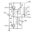
The
図4は、図3の回路300と類似する、回路400を含む。回路400は、破線の箱内に図示される寄生抵抗および寄生インダクタンスを含む。寄生抵抗432および寄生インダクタ434は、ショットキーダイオード342のカソードと出力端子との間で直列に電気的に接続される。ショットキーダイオード342およびコンデンサ362は、電源202の負極端子よりもIGFET322の近くに物理的に位置する。電源202の負極端子とショットキーダイオード342およびコンデンサ362のそれぞれとの間の寄生特徴は、IGFET322とショットキーダイオード342およびコンデンサ362のそれぞれとの間の寄生特徴よりも顕著である。したがって、寄生特徴は、電源202の負極端子とショットキーダイオード342およびコンデンサ362のそれぞれとの間で直列に接続される、寄生抵抗452および寄生インダクタ454を使用してモデル化される。ショットキーダイオード344およびコンデンサ364は、電源202の正極端子よりもIGFET324の近くに物理的に位置する。電源202の正極端子とショットキーダイオード344およびコンデンサ364のそれぞれとの間の寄生特徴は、IGFET324とショットキーダイオード344およびコンデンサ364のそれぞれとの間の寄生特徴よりも顕著である。したがって、寄生特徴は、電源202の正極端子とショットキーダイオード344およびコンデンサ364のそれぞれとの間で直列に接続される、寄生抵抗472および寄生インダクタ474を使用してモデル化される。
FIG. 4 includes a
モデル化する目的で、図1および図4の寄生抵抗は、1mΩ未満の値を割り当てることができ、図1および図4の寄生インダクタは、1nH未満の値を割り当てることができる。インダクタンスは比較的低いが、図1を含む本明細書で説明される回路は、約1MHz程度の周波数で動作するものであり、メモリ等のデジタル論理回路で使用されるトランジスタで一般的に見られる電流よりも1000倍を超えて大きい、顕著な電流を伴う。電圧とインダクタンスとの間の関係は、V=L×(di/dt)であり、したがって、非常に大きいdi/dtの値は、図1の回路に関して分かるように、リンギングを生じさせる可能性がある。 For modeling purposes, the parasitic resistances of FIGS. 1 and 4 can be assigned values less than 1 mΩ, and the parasitic inductors of FIGS. 1 and 4 can be assigned values less than 1 nH. Although the inductance is relatively low, the circuits described herein including FIG. 1 operate at a frequency on the order of about 1 MHz and are commonly found in transistors used in digital logic circuits such as memories. With a noticeable current greater than 1000 times greater than the current. The relationship between voltage and inductance is V = L × (di / dt), so very large di / dt values can cause ringing, as can be seen with respect to the circuit of FIG. is there.
本明細書で説明される回路は、ラップトップコンピュータ、ネットブック、テーブルパーソナルコンピュータ等のモバイル電子デバイスのための、高周波電圧調整器として使用することができる。限定的でない実施形態において、電源は、12VDCの電池とすることができる。モバイル電子デバイスの通常動作中に、電池は、充電器に接続することができ、電源の端子間の電圧は、19V程度の高さに到達する可能性がある。したがって、回路は、そのような電圧に耐えることが必要であり得る。 The circuitry described herein can be used as a high frequency voltage regulator for mobile electronic devices such as laptop computers, netbooks, table personal computers, and the like. In a non-limiting embodiment, the power source can be a 12 VDC battery. During normal operation of the mobile electronic device, the battery can be connected to a charger, and the voltage between the terminals of the power supply can reach as high as 19V. Thus, the circuit may need to withstand such a voltage.
様々な態様および実施形態が可能である。そうした態様および実施形態のいくつかは、下で説明される。本明細書を読んだ後に、当業者は、そうした態様および実施形態が、単なる実例に過ぎず、本発明の範囲を限定するものではないことを認識するであろう。実施形態は、下に列記される付記の任意の1つ以上に従い得る。 Various aspects and embodiments are possible. Some of such aspects and embodiments are described below. After reading this specification, skilled artisans will recognize that such aspects and embodiments are merely illustrative and do not limit the scope of the invention. Embodiments may follow any one or more of the supplementary notes listed below.
付記1.回路は、第1の通電電極および第2の通電電極を有する、第1のスイッチング素子と、第1の通電電極および第2の通電電極を有する、第2のスイッチング素子であって、第2のスイッチング素子の第1の通電電極は、第1のスイッチング素子の第2の通電電極に結合される、第2のスイッチング素子とを含むことができる。回路はさらに、第1の整流素子と、第2の整流素子とを含むことができ、それぞれがアノードおよびカソードを有する。第1の整流素子のアノードは、第1のスイッチング素子の第2の通電電極に結合することができ、かつ第1の整流素子のカソードは、第1のスイッチング素子の第1の通電電極に結合することができる。第2の整流素子のアノードは、第2のスイッチング素子の第2の通電電極に結合することができ、かつ第2の整流素子のカソードは、第2のスイッチング素子の第1の通電電極に結合することができる。回路はなおさらに、第1の端子および第2の端子を有する、第1の電荷蓄積素子を含むことができ、第1の電荷蓄積素子の第1の端子は、第1の整流素子のカソードに結合され、かつ第1の電荷蓄積素子の第2の端子は、第2のスイッチング素子の第2の通電電極に結合される。 Appendix 1. The circuit is a first switching element having a first energizing electrode and a second energizing electrode, and a second switching element having a first energizing electrode and a second energizing electrode, The first energization electrode of the switching element can include a second switching element coupled to the second energization electrode of the first switching element. The circuit can further include a first rectifying element and a second rectifying element, each having an anode and a cathode. The anode of the first rectifying element can be coupled to the second energizing electrode of the first switching element, and the cathode of the first rectifying element is coupled to the first energizing electrode of the first switching element. can do. The anode of the second rectifying element can be coupled to the second energizing electrode of the second switching element, and the cathode of the second rectifying element is coupled to the first energizing electrode of the second switching element. can do. The circuit can further include a first charge storage element having a first terminal and a second terminal, wherein the first terminal of the first charge storage element is connected to the cathode of the first rectifier element. The second terminal of the first charge storage element is coupled to the second current-carrying electrode of the second switching element.
付記2.第1の端子および第2の端子を有する、第2の電荷蓄積素子をさらに含み、第2の電荷蓄積素子の第1の端子は、第1のスイッチング素子の第1の通電電極に結合され、第2の電荷蓄積素子の第2の端子は、第2の整流素子のアノードに結合される、付記1に記載の回路。 Appendix 2. A second charge storage element having a first terminal and a second terminal, wherein the first terminal of the second charge storage element is coupled to the first current-carrying electrode of the first switching element; The circuit of claim 1, wherein the second terminal of the second charge storage element is coupled to the anode of the second rectifying element.
付記3.第1の電荷蓄積素子、第2の電荷蓄積素子、または第1および第2の電荷蓄積素子のそれぞれは、コンデンサを含む、付記2に記載の回路。 Appendix 3. The circuit according to appendix 2, wherein each of the first charge storage element, the second charge storage element, or the first and second charge storage elements includes a capacitor.
付記4.第1の電荷蓄積素子、第2の電荷蓄積素子、または第1および第2の電荷蓄積素子のそれぞれは、少なくとも約80pFの静電容量を有する、付記3に記載の回路。 Appendix 4. The circuit of claim 3, wherein each of the first charge storage element, the second charge storage element, or the first and second charge storage elements has a capacitance of at least about 80 pF.
付記5.第1の電荷蓄積素子、第2の電荷蓄積素子、または第1および第2の電荷蓄積素子のそれぞれは、約1.5nF〜約40nFの範囲の静電容量を有する、付記3に記載の回路。 Appendix 5. The circuit of claim 3, wherein each of the first charge storage element, the second charge storage element, or the first and second charge storage elements has a capacitance in the range of about 1.5 nF to about 40 nF. .
付記6.第1の電荷蓄積素子、第2の電荷蓄積素子、または第1および第2の電荷蓄積素子のそれぞれは、特定の静電容量を有し、第1のスイッチング素子、第2のスイッチング素子、または第1および第2のスイッチング素子のそれぞれは、その対応する第1および第2の通電電極間に静電容量を有し、特定の静電容量と、その対応する第1および第2の通電電極間の静電容量との比率は、少なくとも1.5:1である、付記3に記載の回路。 Appendix 6. Each of the first charge storage element, the second charge storage element, or the first and second charge storage elements has a specific capacitance, and the first switching element, the second switching element, or Each of the first and second switching elements has a capacitance between the corresponding first and second energization electrodes, and the specific capacitance and the corresponding first and second energization electrodes. The circuit according to appendix 3, wherein the ratio between the capacitance and the capacitance is at least 1.5: 1.
付記7.第1の整流素子、第2の整流素子、または第1および第2の整流素子のそれぞれは、ショットキーダイオードまたはpn接合ダイオードを含む、付記1に記載の回路。 Appendix 7. The circuit according to appendix 1, wherein each of the first rectifier element, the second rectifier element, or the first and second rectifier elements includes a Schottky diode or a pn junction diode.
付記8.第1の整流素子、第2の整流素子、または第1および第2の整流素子のそれぞれは、並列に電気的に接続されるショットキーダイオードおよびpn接合ダイオードを含む、付記1に記載の回路。 Appendix 8. The circuit according to appendix 1, wherein each of the first rectifier element, the second rectifier element, or the first and second rectifier elements includes a Schottky diode and a pn junction diode electrically connected in parallel.
付記9.第1の整流素子は、第1のスイッチング素子のドレイン−ソース間絶縁破壊電圧の約2.0倍以下である絶縁破壊電圧を有し、第2の整流素子は、第2のスイッチング素子のドレイン−ソース間絶縁破壊電圧の約2.0倍以下である絶縁破壊電圧を有する、付記8に記載の回路。 Appendix 9. The first rectifying element has a breakdown voltage that is about 2.0 times or less the drain-source breakdown voltage of the first switching element, and the second rectifying element is a drain of the second switching element. The circuit according to appendix 8, wherein the circuit has a breakdown voltage that is not more than about 2.0 times a breakdown voltage between sources.
付記10.第1のスイッチング素子は、ゲートを含む、絶縁ゲート型電界効果トランジスタであり、第1のスイッチング素子の第1の通電電極は、ドレインであり、第1のトランジスタの第2の通電電極は、ソースであり、第2のスイッチング素子は、ゲートを含む、別の絶縁ゲート型電界効果トランジスタであり、第2のスイッチング素子の第1の通電電極は、ドレインであり、第2のスイッチング素子の第2の通電電極は、ソースである、付記1に記載の回路。
付記11.回路は、電圧調整器のスイッチング回路である、付記1に記載の回路。 Appendix 11. The circuit according to appendix 1, wherein the circuit is a switching circuit of a voltage regulator.
付記12.回路は、第1の通電電極および第2の通電電極を有する、ハイサイドトランジスタと、第1の通電電極および第2の通電電極を有する、ローサイドトランジスタとを含むことができ、ローサイドトランジスタの第1の通電電極は、ハイサイドトランジスタの第2の通電電極に結合される。回路はさらに、アノードおよびカソードを有する、整流素子をさらに含むことができ、整流素子のアノードは、ハイサイドトランジスタの第2の通電電極に結合され、整流素子のカソードは、ハイサイドトランジスタの第1の通電電極に結合される。回路はなおさらに、第1の端子および第2の端子を有する、電荷蓄積素子を含み、電荷蓄積素子の第1の端子は、ハイサイドトランジスタの第1の通電電極に結合され、電荷蓄積素子の第2の端子は、ローサイドトランジスタの第2の通電電極に結合される。 Appendix 12. The circuit can include a high-side transistor having a first energizing electrode and a second energizing electrode, and a low-side transistor having a first energizing electrode and a second energizing electrode. The current-carrying electrode is coupled to the second current-carrying electrode of the high-side transistor. The circuit may further include a rectifying element having an anode and a cathode, the anode of the rectifying element being coupled to the second current-carrying electrode of the high-side transistor, and the cathode of the rectifying element being the first of the high-side transistor. Are coupled to the current-carrying electrode. The circuit still further includes a charge storage element having a first terminal and a second terminal, the first terminal of the charge storage element being coupled to the first current-carrying electrode of the high-side transistor, The second terminal is coupled to the second energizing electrode of the low side transistor.
付記13.電荷蓄積素子は、コンデンサを含む、付記12に記載の回路。 Appendix 13. The circuit according to appendix 12, wherein the charge storage element includes a capacitor.
付記14.電荷蓄積素子は、静電容量を有し、ハイサイドトランジスタ、ローサイドトランジスタ、またはハイサイドおよびローサイドトランジスタのそれぞれは、その対応する第1および第2の通電電極間に静電容量を有し、静電容量と、その対応する第1および第2の通電電極間の静電容量との比率は、少なくとも1.5:1である、付記13に記載の回路。 Appendix 14. The charge storage element has a capacitance, and each of the high-side transistor, the low-side transistor, or the high-side and low-side transistor has a capacitance between its corresponding first and second current-carrying electrodes. The circuit according to appendix 13, wherein the ratio between the capacitance and the corresponding capacitance between the first and second energization electrodes is at least 1.5: 1.
付記15.整流素子は、並列に電気的に接続されるショットキーダイオードおよびpnダイオードを含む、付記12に記載の回路。 Appendix 15. The circuit according to appendix 12, wherein the rectifying element includes a Schottky diode and a pn diode electrically connected in parallel.
付記16.整流素子は、ハイサイドトランジスタのドレイン−ソース間絶縁破壊電圧の約2.0倍以下である絶縁破壊電圧を有する、付記15に記載の回路。 Appendix 16. The circuit according to appendix 15, wherein the rectifying element has a breakdown voltage that is not more than about 2.0 times a drain-source breakdown voltage of the high-side transistor.
付記17.スイッチング回路は、ハイサイドトランジスタおよびローサイドトランジスタを含むことができ、それぞれがソース、ゲート、およびドレインを有する。ハイサイドトランジスタのドレインは、第1の電力端子に電気的に接続することができ、ハイサイドトランジスタのゲートは、スイッチング回路の第1の入力に電気的に接続することができ、ハイサイドトランジスタのソースは、スイッチング回路の出力端子に電気的に接続することができる。ローサイドトランジスタのドレインは、出力端子に電気的に接続することができ、ローサイドトランジスタのゲートは、スイッチング回路の第2の入力に電気的に接続することができ、ローサイドトランジスタのソースは、第2の電力端子に電気的に接続することができる。スイッチング回路はさらに、第1のショットキーダイオードと、第2のショットキーダイオードとを含むことができ、それぞれがアノードおよびカソードを有する。第1のショットキーダイオードのアノードは、出力端子に電気的に接続することができ、第1のショットキーダイオードのカソードは、第1の電力端子に電気的に接続することができ、第2のショットキーダイオードのアノードは、第2の電力端子に電気的に接続することができ、ショットキーダイオードのカソードは、出力端子に電気的に接続することができる。スイッチング回路はなおさらに、第1のコンデンサと、第2のコンデンサとを含むことができ、それぞれが第1の端子および第2の端子を有する。第1のコンデンサの第1の端子は、第1の電力端子に電気的に接続することができ、第1のコンデンサの第2の端子は、第2の電力端子に電気的に接続することができ、第2のコンデンサの第1の端子は、第1の電力端子に電気的に接続することができ、第2のコンデンサの第2の端子は、第2の電力端子に電気的に接続することができる。 Appendix 17. The switching circuit can include a high side transistor and a low side transistor, each having a source, a gate, and a drain. The drain of the high side transistor can be electrically connected to the first power terminal, and the gate of the high side transistor can be electrically connected to the first input of the switching circuit. The source can be electrically connected to the output terminal of the switching circuit. The drain of the low-side transistor can be electrically connected to the output terminal, the gate of the low-side transistor can be electrically connected to the second input of the switching circuit, and the source of the low-side transistor is the second It can be electrically connected to the power terminal. The switching circuit can further include a first Schottky diode and a second Schottky diode, each having an anode and a cathode. The anode of the first Schottky diode can be electrically connected to the output terminal, the cathode of the first Schottky diode can be electrically connected to the first power terminal, and the second The anode of the Schottky diode can be electrically connected to the second power terminal, and the cathode of the Schottky diode can be electrically connected to the output terminal. The switching circuit can still further include a first capacitor and a second capacitor, each having a first terminal and a second terminal. The first terminal of the first capacitor can be electrically connected to the first power terminal, and the second terminal of the first capacitor can be electrically connected to the second power terminal. The first terminal of the second capacitor can be electrically connected to the first power terminal, and the second terminal of the second capacitor is electrically connected to the second power terminal. be able to.
付記18.第1および第2のコンデンサのそれぞれは、約1.5nF〜約40nFの範囲の静電容量を有する、付記17に記載の回路。 Appendix 18. The circuit of clause 17, wherein each of the first and second capacitors has a capacitance in the range of about 1.5 nF to about 40 nF.
付記19.第1および第2のショットキーダイオードのそれぞれは、ローサイドおよびハイサイドトランジスタのそれぞれのドレイン−ソース間絶縁破壊電圧の約2.0倍以下の絶縁破壊電圧を有する、付記17に記載の回路。
実施例
Appendix 19. 18. The circuit according to appendix 17, wherein each of the first and second Schottky diodes has a breakdown voltage not more than about 2.0 times a drain-source breakdown voltage of each of the low-side and high-side transistors.
Example
本明細書で説明される概念はさらに実施例において説明されるが、特許請求の範囲で説明される本発明の範囲を限定するものではない。実施例は、電力スイッチング回路の出力端子でのリンギングを低減させるために、整流素子および電荷蓄積コンデンサの組み合わせを使用できることを実証する。 The concepts described herein are further described in the examples, which do not limit the scope of the invention described in the claims. The example demonstrates that a combination of a rectifying element and a charge storage capacitor can be used to reduce ringing at the output terminal of the power switching circuit.
図1および図4の回路は、図5のタイミング図のデータを生成するために使用される。以下の値は、図1および図4の寄生抵抗およびインダクタに割り当てられる。 The circuits of FIGS. 1 and 4 are used to generate data for the timing diagram of FIG. The following values are assigned to the parasitic resistances and inductors of FIGS.
寄生抵抗132、250μΩ、
寄生インダクタ134、300pH、
寄生抵抗432、250μΩ、
寄生インダクタ434、300pH、
寄生抵抗452、25mΩ、
寄生インダクタ454、150pH、 Parasitic inductor 454, 150 pH,
寄生抵抗472、50mΩ、および
寄生インダクタ474、250pH。 Parasitic inductor 474, 250 pH.
図5は、電源がその端子の間で19Vであるときにスイッチング事象が起こった後の時間の関数としてVoutを提供する、出力端子上の電圧を比較する、タイミング図である。t=0で、IGFET122はオフであり、IGFET124はオンである。出力端子上の電圧は、約0Vである。t=約15ナノ秒で、IGFET124をオフにし、次いで、IGFET122をオンにする。t=0でIGFET322はオフでIGFET324はオンである。出力端子上の電圧は、約0Vである。t=約15ナノ秒で、IGFET324をオフにし、次いで、IGFET322をオンにする。理想的には、出力端子上の電圧は、いかなる電圧オーバーシュート、電圧アンダーシュート、またはリンギングも伴わずに、0Vから19Vに即座に上昇する。図1および図4で図示される回路は理想的なものではなく、したがって、電圧オーバーシュート、電圧アンダーシュート、およびリンギングが起こる。
FIG. 5 is a timing diagram comparing the voltage on the output terminal providing V out as a function of time after a switching event occurs when the power supply is 19V between its terminals. At t = 0,
明らかに、図4の回路400は、図1の回路100と比較して、かなり良好な性能を提供する。コンデンサ362,364は、急速に充電することができ、過剰な電荷を蓄積することを可能にすることができ、そして電圧オーバーシュートおよび電圧アンダーシュートの量を低減させることができる。ショットキーダイオード342,344は、電圧オーバーシュートまたは電圧アンダーシュート中に、低インピーダンスの電流経路をコンデンサ362,364に提供するのを補助する一方で、出力端子が、電源の正極端子および負極端子上の電圧に等しいか、またはそれらの間の電圧であるときに、電流を遮断する。図1の回路100のように、コンデンサ362,364、ならびにショットキーダイオード342,344を伴っていなければ、Voutは、34Vに達する可能性があり、それは、IGFET124の30Vというドレイン−ソース間絶縁破壊電圧を超える。図4の回路400のように、コンデンサ362,364、ならびにショットキーダイオード342,344を伴っていれば、Voutは、26Vに達することになり、それは、IGFET324の30Vというドレイン−ソース間絶縁破壊電圧未満である。さらに、図4の回路400の出力端子で見られるリンギングは、少なくとも15ナノ秒でほぼなくなり、図1の回路100の出力端子の場合よりも早い。
Clearly, the
以下に示す構成は、本発明の実施態様の例を示す。 The following configuration shows an example of an embodiment of the present invention.
回路において、
第1の通電電極および第2の通電電極を有する、第1のスイッチング素子と、
第1の通電電極および第2の通電電極を有する、第2のスイッチング素子であって、前記第2のスイッチング素子の前記第1の通電電極は、前記第1のスイッチング素子の前記第2の通電電極に結合される、第2のスイッチング素子と、
アノードおよびカソードを有する、第1の整流素子であって、前記第1の整流素子の前記アノードは、前記第1のスイッチング素子の前記第2の通電電極に結合され、前記第1の整流素子の前記カソードは、前記第1のスイッチング素子の前記第1の通電電極に結合される、第1の整流素子と、
アノードおよびカソードを有する、第2の整流素子であって、前記第2の整流素子の前記アノードは、前記第2のスイッチング素子の前記第2の通電電極に結合され、前記第2の整流素子の前記カソードは、前記第2のスイッチング素子の前記第1の通電電極に結合される、第2の整流素子と、
第1の端子および第2の端子を有する、第1の電荷蓄積素子であって、前記第1の電荷蓄積素子の前記第1の端子は、前記第1の整流素子の前記カソードに結合され、前記第1の電荷蓄積素子の前記第2の端子は、前記第2のスイッチング素子の前記第2の通電電極に結合される、第1の電荷蓄積素子と、
を備えることを特徴とする回路(米国特許出願(13/794,038)の出願時の請求項1に対応、以下同様)。
In the circuit
A first switching element having a first energizing electrode and a second energizing electrode;
A second switching element having a first energization electrode and a second energization electrode, wherein the first energization electrode of the second switching element is the second energization of the first switching element. A second switching element coupled to the electrode;
A first rectifying element having an anode and a cathode, wherein the anode of the first rectifying element is coupled to the second energizing electrode of the first switching element; The cathode is coupled to the first current-carrying electrode of the first switching element;
A second rectifier element having an anode and a cathode, wherein the anode of the second rectifier element is coupled to the second current-carrying electrode of the second switching element; The cathode is coupled to the first current-carrying electrode of the second switching element;
A first charge storage element having a first terminal and a second terminal, wherein the first terminal of the first charge storage element is coupled to the cathode of the first rectifier element; The second terminal of the first charge storage element is coupled to the second energization electrode of the second switching element;
(Corresponding to claim 1 at the time of filing of US patent application (13 / 794,038), the same applies hereinafter)
第1の端子および第2の端子を有する、第2の電荷蓄積素子をさらに備え、前記第2の電荷蓄積素子の前記第1の端子は、前記第1のスイッチング素子の前記第1の通電電極に結合され、前記第2の電荷蓄積素子の前記第2の端子は、前記第2の整流素子の前記アノードに結合されることを特徴とする、段落0068に記載された回路(請求項2に対応)。 And a second charge storage element having a first terminal and a second terminal, wherein the first terminal of the second charge storage element is the first current-carrying electrode of the first switching element. The circuit of claim 0068, wherein the second terminal of the second charge storage element is coupled to the anode of the second rectifying element. Correspondence).
前記第1の電荷蓄積素子、前記第2の電荷蓄積素子、または前記第1および第2の電荷蓄積素子のそれぞれは、コンデンサを含む、段落0069に記載された回路(請求項3に対応)。 The circuit of paragraph 0069 (corresponding to claim 3), wherein each of the first charge storage element, the second charge storage element, or the first and second charge storage elements includes a capacitor.
前記第1の電荷蓄積素子、前記第2の電荷蓄積素子、または前記第1および第2の電荷蓄積素子のそれぞれは、少なくとも約80pFの静電容量を有する、段落0070に記載された回路(請求項4に対応)。 The circuit of paragraph 0070, wherein each of the first charge storage device, the second charge storage device, or each of the first and second charge storage devices has a capacitance of at least about 80 pF. Corresponds to item 4).
前記第1の電荷蓄積素子、前記第2の電荷蓄積素子、または前記第1および第2の電荷蓄積素子のそれぞれは、約1.5nF〜約40nFの範囲の静電容量を有する、段落0070に記載された回路(請求項5に対応)。 Paragraph 0070, wherein each of the first charge storage element, the second charge storage element, or the first and second charge storage elements has a capacitance ranging from about 1.5 nF to about 40 nF. The described circuit (corresponding to claim 5).
前記第1の電荷蓄積素子、前記第2の電荷蓄積素子、または前記第1および第2の電荷蓄積素子のそれぞれは、特定の静電容量を有し、前記第1のスイッチング素子、前記第2のスイッチング素子、または前記第1および第2のスイッチング素子のそれぞれは、その対応する第1および第2の通電電極間に静電容量を有し、前記特定の静電容量と、前記その対応する第1および第2の通電電極間の特定の静電容量との比率は、少なくとも1.5:1である、段落0070に記載された回路(請求項6に対応)。 Each of the first charge storage element, the second charge storage element, or the first and second charge storage elements has a specific capacitance, the first switching element, the second charge storage element Each of the switching elements, or each of the first and second switching elements, has a capacitance between the corresponding first and second energization electrodes, and the specific capacitance and the corresponding The circuit of paragraph 0070 (corresponding to claim 6), wherein the ratio of the specific capacitance between the first and second energizing electrodes is at least 1.5: 1.
前記第1の整流素子、前記第2の整流素子、または前記第1および第2の整流素子のそれぞれは、ショットキーダイオードまたはpn接合ダイオードを含む、段落0068に記載された回路(請求項7に対応)。 The circuit of paragraph 0068, wherein each of the first rectifier element, the second rectifier element, or the first and second rectifier elements includes a Schottky diode or a pn junction diode (in claim 7). Correspondence).
前記第1の整流素子、前記第2の整流素子、または前記第1および第2の整流素子の回路のそれぞれは、並列に電気的に接続されるショットキーダイオードおよびpn接合ダイオードを含む、段落0068に記載された回路(請求項8に対応)。 Paragraph 0068, each of the first rectifier element, the second rectifier element, or the first and second rectifier circuit includes a Schottky diode and a pn junction diode electrically connected in parallel. The circuit according to claim 8 (corresponding to claim 8).
前記第1の整流素子は、前記第1のスイッチング素子のドレイン−ソース間絶縁破壊電圧の約2.0倍以下である絶縁破壊電圧を有し、
前記第2の整流素子は、前記第2のスイッチング素子のドレイン−ソース間絶縁破壊電圧の約2.0倍以下である絶縁破壊電圧を有する、段落0075に記載された回路(請求項9に対応)。
The first rectifying element has a breakdown voltage that is about 2.0 times or less of a drain-source breakdown voltage of the first switching element;
The circuit of paragraph 0075, wherein the second rectifying element has a breakdown voltage that is not more than about 2.0 times a drain-source breakdown voltage of the second switching element (corresponding to claim 9). ).
前記第1のスイッチング素子は、ゲートを含む、絶縁ゲート型電界効果トランジスタであり、前記第1のスイッチング素子の前記第1の通電電極は、ドレインであり、前記第1のトランジスタの前記第2の通電電極は、ソースであり、
前記第2のスイッチング素子は、ゲートを含む、別の絶縁ゲート型電界効果トランジスタであり、前記第2のスイッチング素子の前記第1の通電電極は、ドレインであり、前記第2のスイッチング素子の前記第2の通電電極は、ソースである、段落0068に記載された回路(請求項10に対応)。
The first switching element is an insulated gate field effect transistor including a gate, the first current-carrying electrode of the first switching element is a drain, and the second transistor of the first transistor The energizing electrode is the source
The second switching element is another insulated gate field effect transistor including a gate, the first conducting electrode of the second switching element is a drain, and the second switching element is the drain of the second switching element. The circuit of paragraph 0068, wherein the second energizing electrode is a source (corresponding to claim 10).
前記回路は、電圧調整器のスイッチング回路である、段落0068に記載された回路(請求項11に対応)。 The circuit of paragraph 0068, wherein the circuit is a voltage regulator switching circuit (corresponding to claim 11).
回路において、
第1の通電電極および第2の通電電極を有する、ハイサイドトランジスタと、
第1の通電電極および第2の通電電極を有する、ローサイドトランジスタであって、前記ローサイドトランジスタの前記第1の通電電極は、前記ハイサイドトランジスタの前記第2の通電電極に結合される、ローサイドトランジスタと、
アノードおよびカソードを有する整流素子であって、前記整流素子の前記アノードは、前記ハイサイドトランジスタの前記第2の通電電極に結合され、前記整流素子の前記カソードは、前記ハイサイドトランジスタの前記第1の通電電極に結合される、整流素子と、
第1の端子および第2の端子を有する、電荷蓄積素子であって、前記電荷蓄積素子の前記第1の端子は、前記ハイサイドトランジスタの前記第1の通電電極に結合され、前記電荷蓄積素子の前記第2の端子は、前記ローサイドトランジスタの前記第2の通電電極に結合される、電荷蓄積素子と、
を備える、回路(請求項12に対応)。
In the circuit
A high side transistor having a first energizing electrode and a second energizing electrode;
A low-side transistor having a first conducting electrode and a second conducting electrode, wherein the first conducting electrode of the low-side transistor is coupled to the second conducting electrode of the high-side transistor When,
A rectifying element having an anode and a cathode, wherein the anode of the rectifying element is coupled to the second conducting electrode of the high-side transistor, and the cathode of the rectifying element is the first of the high-side transistor. A rectifying element coupled to a current-carrying electrode;
A charge storage element having a first terminal and a second terminal, wherein the first terminal of the charge storage element is coupled to the first current-carrying electrode of the high-side transistor, and the charge storage element A charge storage element coupled to the second energizing electrode of the low-side transistor;
A circuit (corresponding to claim 12).
前記電荷蓄積素子は、コンデンサを含む、段落0079に記載された回路(請求項13に対応)。 The circuit of paragraph 0079, wherein the charge storage element includes a capacitor (corresponding to claim 13).
前記電荷蓄積素子は、静電容量を有し、前記ハイサイドトランジスタ、前記ローサイドトランジスタ、または前記ハイサイドおよびローサイドトランジスタのそれぞれは、その対応する第1および第2の通電電極間に静電容量を有し、前記静電容量と、前記その対応する第1および第2の通電電極間の静電容量との比率は、少なくとも1.5:1である、段落0080に記載された回路(請求項14に対応)。 The charge storage element has a capacitance, and each of the high-side transistor, the low-side transistor, or the high-side and low-side transistors has a capacitance between its corresponding first and second current-carrying electrodes. The circuit of claim 0080, wherein the ratio of the capacitance to the capacitance between the corresponding first and second energizing electrodes is at least 1.5: 1. 14).
前記整流素子は、並列に電気的に接続されるショットキーダイオードおよびpn接合ダイオードを含む、段落0079に記載された回路(請求項15に対応)。 The circuit of paragraph 0079 (corresponding to claim 15), wherein the rectifying element includes a Schottky diode and a pn junction diode electrically connected in parallel.
前記整流素子は、前記ハイサイドトランジスタのドレイン−ソース間絶縁破壊電圧の約2.0倍以下である絶縁破壊電圧を有する、段落0082に記載された回路(請求項16に対応)。 The circuit of paragraph 0082 (corresponding to claim 16), wherein the rectifying element has a breakdown voltage that is not more than about 2.0 times a drain-source breakdown voltage of the high-side transistor.
スイッチング回路において、
ソース、ゲート、およびドレインを有する、ハイサイドトランジスタであって、
前記ハイサイドトランジスタの前記ドレインは、第1の電力端子に電気的に接続され、
前記ハイサイドトランジスタの前記ゲートは、前記スイッチング回路の第1の入力に電気的に接続され、
前記ハイサイドトランジスタの前記ソースは、前記スイッチング回路の出力端子に電気的に接続される、ハイサイドトランジスタと、
ソース、ゲート、およびドレインを有する、ローサイドトランジスタであって、
前記ローサイドトランジスタの前記ドレインは、前記出力端子に電気的に接続され、
前記ローサイドトランジスタの前記ゲートは、前記スイッチング回路の第2の入力に電気的に接続され、
前記ローサイドトランジスタの前記ソースは、第2の電力端子に電気的に接続される、ローサイドトランジスタと、
アノードおよびカソードを有する、第1のショットキーダイオードであって、前記第1のショットキーダイオードの前記アノードは、前記出力端子に電気的に接続され、前記第1のショットキーダイオードの前記カソードは、前記第1の電力端子に電気的に接続される、第1のショットキーダイオードと、
アノードおよびカソードを有する、第2のショットキーダイオードであって、前記第2のショットキーダイオードの前記アノードは、前記第2の電力端子に電気的に接続され、前記ショットキーダイオードの前記カソードは、前記出力端子に電気的に接続される、第2のショットキーダイオードと、
第1の端子および第2の端子を有する、第1のコンデンサであって、前記第1のコンデンサの前記第1の端子は、前記第1の電力端子に電気的に接続され、前記第1のコンデンサの前記第2の端子は、前記第2の電力端子に電気的に接続される、第1のコンデンサと、
第1の端子および第2の端子を有する、第2のコンデンサであって、前記第2のコンデンサの前記第1の端子は、前記第1の電力端子に電気的に接続され、前記第2のコンデンサの前記第2の端子は、前記第2の電力端子に電気的に接続される、第2のコンデンサと、
を備える、スイッチング回路(請求項17に対応)。
In the switching circuit,
A high-side transistor having a source, a gate, and a drain,
The drain of the high-side transistor is electrically connected to a first power terminal;
The gate of the high-side transistor is electrically connected to a first input of the switching circuit;
The source of the high side transistor is electrically connected to the output terminal of the switching circuit; and
A low-side transistor having a source, a gate, and a drain comprising:
The drain of the low-side transistor is electrically connected to the output terminal;
The gate of the low-side transistor is electrically connected to a second input of the switching circuit;
The source of the low side transistor is electrically connected to a second power terminal;
A first Schottky diode having an anode and a cathode, wherein the anode of the first Schottky diode is electrically connected to the output terminal, and the cathode of the first Schottky diode is A first Schottky diode electrically connected to the first power terminal;
A second Schottky diode having an anode and a cathode, wherein the anode of the second Schottky diode is electrically connected to the second power terminal, and the cathode of the Schottky diode is A second Schottky diode electrically connected to the output terminal;
A first capacitor having a first terminal and a second terminal, wherein the first terminal of the first capacitor is electrically connected to the first power terminal; The second terminal of the capacitor is electrically connected to the second power terminal; the first capacitor;
A second capacitor having a first terminal and a second terminal, wherein the first terminal of the second capacitor is electrically connected to the first power terminal; A second capacitor, wherein the second terminal of the capacitor is electrically connected to the second power terminal;
A switching circuit (corresponding to claim 17).
前記第1および第2のコンデンサのそれぞれは、約1.5nF〜約40nFの範囲の静電容量を有する、段落0084に記載されたスイッチング回路(請求項18に対応)。 The switching circuit of paragraph 0084 (corresponding to claim 18), wherein each of the first and second capacitors has a capacitance in the range of about 1.5 nF to about 40 nF.
前記第1および第2のショットキーダイオードのそれぞれは、前記ローサイドおよびハイサイドトランジスタのそれぞれのドレイン−ソース間絶縁破壊電圧の約2.0倍以下の絶縁破壊電圧を有する、段落0084に記載されたスイッチング回路(請求項19に対応)。 Each of the first and second Schottky diodes is described in paragraph 0084, wherein each of the low-side and high-side transistors has a breakdown voltage that is not more than about 2.0 times a drain-source breakdown voltage. A switching circuit (corresponding to claim 19);
概要または実施例において上で説明される行為の全てが必要とされるわけではなく、特定の行為の一部が必要とされない場合があること、また、1つ以上のさらなる行為が、上で説明した行為に加えて行われ得ることに留意されたい。さらに、行為が列記される順序は、必ずしもそれらが行われる順序であるとは限らない。 Not all of the acts described above in the summary or example are required, and some of the specific acts may not be required, and one or more additional acts are described above. It should be noted that this can be done in addition to the act performed. Furthermore, the order in which actions are listed is not necessarily the order in which they are performed.
利益、他の長所、および問題点に対する解決策を特定の実施形態に関して上で説明してきた。しかしながら、利益、長所、問題点の解決策、およびあらゆる利益、長所、または解決策を生じさせ得る、あるいはより明白にさせ得るあらゆる特徴は、特許請求の範囲のいずれかまたは全ての重要な、必要な、または必須の特徴として解釈されるべきではない。 Benefits, other advantages, and solutions to problems have been described above with regard to specific embodiments. However, benefits, advantages, solutions to problems, and any features that may produce or make more obvious any benefit, advantage, or solution are important and necessary for any or all of the claims. It should not be interpreted as an essential or essential feature.
本明細書で説明される実施形態の仕様および具体例は、種々の実施形態の構造の一般的な理解を提供することを意図する。本仕様および具体例は、本明細書で説明される構造または方法を使用する装置およびシステムの要素および特徴の全ての網羅的かつ包括的な説明としての役割を果たすことを意図しない。特定の特徴は、明確にするために、別個の実施形態の状況において本明細書で説明されており、また、単一の実施形態において組み合わせて提供され得る。逆に、簡潔にするために、1つの実施形態の状況において説明される種々の特徴はまた、別々に提供されるか、またはあらゆる副次的な組み合わせでも提供され得る。さらに、範囲で提示される値への言及は、その範囲内のあらゆる値を含む。本明細書を読み終わった後にだけ、多くの他の実施形態が当業者に明らかになり得る。故に、本開示は、限定的ではなく例示的なものとみなされるべきである。 The specifications and specific examples of the embodiments described herein are intended to provide a general understanding of the structure of the various embodiments. This specification and specific examples are not intended to serve as an exhaustive and comprehensive description of all of the elements and features of apparatus and systems that use the structures or methods described herein. Certain features are described herein in the context of separate embodiments for clarity, and may be provided in combination in a single embodiment. Conversely, for the sake of brevity, the various features described in the context of one embodiment may also be provided separately or in any sub-combination. Furthermore, references to values presented in ranges include every value within that range. Many other embodiments will be apparent to those skilled in the art only after reading this specification. Accordingly, the present disclosure should be regarded as illustrative rather than limiting.
200 回路
202 電源
222,224 スイッチング素子
242,244 整流素子
262,264 電荷蓄積素子
322,324 nチャネルIGFET
342,344 ショットキーダイオード
362,364 コンデンサ
474 寄生インダクタ
200
342,344 Schottky diode 362,364 Capacitor 474 Parasitic inductor
Claims (5)
第1の通電電極および第2の通電電極を有する第1のスイッチング素子と、
第1の通電電極および第2の通電電極を有する第2のスイッチング素子であって、前記第2のスイッチング素子の前記第1の通電電極は、前記第1のスイッチング素子の前記第2の通電電極に結合される、第2のスイッチング素子と、
アノードおよびカソードを有する第1の整流素子であって、前記第1の整流素子の前記カソードは、前記第1のスイッチング素子の前記第2の通電電極に結合される、第1の整流素子と、
アノードおよびカソードを有する第2の整流素子であって、前記第2の整流素子の前記アノードは、前記第2のスイッチング素子の前記第1の通電電極に結合される、第2の整流素子と、
第1の端子および第2の端子を有する第1の電荷蓄積素子であって、前記第1の電荷蓄積素子の前記第1の端子は、前記第1のスイッチング素子の前記第1の通電電極に結合され、前記第1の電荷蓄積素子の前記第2の端子は、前記第1の整流素子の前記アノードに結合される、第1の電荷蓄積素子と、
第1の端子および第2の端子を有する第2の電荷蓄積素子であって、前記第2の電荷蓄積素子の前記第1の端子は、前記第2の整流素子の前記カソードに結合され、前記第2の電荷蓄積素子の前記第2の端子は、前記第2のスイッチング素子の前記第2の通電電極に結合される、第2の電荷蓄積素子と、を備え、
前記回路の負極端子と前記第1の電荷蓄積素子との間の寄生特徴は、前記第1のスイッチング素子と前記第1の電荷蓄積素子との間の寄生特徴より大きいか、あるいは、
前記回路の正極端子と前記第2の電荷蓄積素子との間の寄生特徴は、前記第2のスイッチング素子と前記第2の電荷蓄積素子との間の寄生特徴より大きい、
ことを特徴とする回路。 In the circuit
A first switching element having a first energizing electrode and a second energizing electrode;
A second switching element having a first energizing electrode and a second energizing electrode, wherein the first energizing electrode of the second switching element is the second energizing electrode of the first switching element. A second switching element coupled to
A first rectifying element having an anode and a cathode, wherein the cathode of the first rectifying element is coupled to the second energizing electrode of the first switching element;
A second rectifying element having an anode and a cathode, wherein the anode of the second rectifying element is coupled to the first energizing electrode of the second switching element;
A first charge storage element having a first terminal and a second terminal, wherein the first terminal of the first charge storage element is connected to the first current-carrying electrode of the first switching element. A first charge storage element coupled, wherein the second terminal of the first charge storage element is coupled to the anode of the first rectifying element;
A second charge storage element having a first terminal and a second terminal, wherein the first terminal of the second charge storage element is coupled to the cathode of the second rectifier element; The second terminal of the second charge storage element comprises a second charge storage element coupled to the second energization electrode of the second switching element;
A parasitic characteristic between the negative terminal of the circuit and the first charge storage element is greater than a parasitic characteristic between the first switching element and the first charge storage element; or
A parasitic characteristic between the positive terminal of the circuit and the second charge storage element is greater than a parasitic characteristic between the second switching element and the second charge storage element;
A circuit characterized by that.
第1の通電電極および第2の通電電極を有するハイサイドトランジスタと、
第1の通電電極および第2の通電電極を有するローサイドトランジスタであって、前記ローサイドトランジスタの前記第1の通電電極は、前記ハイサイドトランジスタの前記第2の通電電極に結合される、ローサイドトランジスタと、
アノードおよびカソードを有する第1の整流素子であって、前記第1の整流素子の前記カソードは、前記ハイサイドトランジスタの前記第2の通電電極に結合される、第1の整流素子と、
アノードおよびカソードを有する第2の整流素子であって、前記第2の整流素子の前記アノードは、前記ローサイドトランジスタの前記第1の通電電極に結合される、第2の整流素子と、
第1の端子および第2の端子を有する第1の電荷蓄積素子であって、前記第1の電荷蓄積素子の前記第1の端子は、前記ハイサイドトランジスタの前記第1の通電電極に結合され、前記第1の電荷蓄積素子の前記第2の端子は、前記第1の整流素子の前記アノードに結合される、第1の電荷蓄積素子と、
第1の端子および第2の端子を有する第2の電荷蓄積素子であって、前記第2の電荷蓄積素子の前記第1の端子は、前記第2の整流素子の前記カソードに結合され、前記第2の電荷蓄積素子の前記第2の端子は、前記ローサイドトランジスタの前記第2の通電電極に結合される、第2の電荷蓄積素子と、を備え、
前記回路の負極端子と前記第1の電荷蓄積素子との間の寄生特徴は、前記ハイサイドトランジスタと前記第1の電荷蓄積素子との間の寄生特徴より大きいか、あるいは、
前記回路の正極端子と前記第2の電荷蓄積素子との間の寄生特徴は、前記ローサイドトランジスタと前記第2の電荷蓄積素子との間の寄生特徴より大きく、
前記第1の整流素子は、前記回路の負極端子より前記ハイサイドトランジスタに近接するか、あるいは、
前記第2の整流素子は、前記回路の正極端子より前記ローサイドトランジスタに近接する、
ことを特徴とする回路。 In the circuit
A high side transistor having a first energizing electrode and a second energizing electrode;
A low-side transistor having a first energization electrode and a second energization electrode, wherein the first energization electrode of the low-side transistor is coupled to the second energization electrode of the high-side transistor; ,
A first rectifying element having an anode and a cathode, wherein the cathode of the first rectifying element is coupled to the second energizing electrode of the high-side transistor;
A second rectifying element having an anode and a cathode, wherein the anode of the second rectifying element is coupled to the first current-carrying electrode of the low-side transistor;
A first charge storage element having a first terminal and a second terminal, wherein the first terminal of the first charge storage element is coupled to the first current-carrying electrode of the high-side transistor. The second terminal of the first charge storage element is coupled to the anode of the first rectifier element; and
A second charge storage element having a first terminal and a second terminal, wherein the first terminal of the second charge storage element is coupled to the cathode of the second rectifier element; The second terminal of the second charge storage element comprises a second charge storage element coupled to the second current-carrying electrode of the low-side transistor;
A parasitic characteristic between the negative terminal of the circuit and the first charge storage element is greater than a parasitic characteristic between the high-side transistor and the first charge storage element; or
The parasitic characteristic between the positive terminal of the circuit and the second charge storage element is larger than the parasitic characteristic between the low-side transistor and the second charge storage element,
The first rectifying element is closer to the high-side transistor than the negative terminal of the circuit, or
The second rectifying element is closer to the low-side transistor than the positive terminal of the circuit.
A circuit characterized by that.
ソース、ゲート、およびドレインを有するハイサイドトランジスタであって、
前記ハイサイドトランジスタの前記ドレインは、第1の電力端子に電気的に接続され、
前記ハイサイドトランジスタの前記ゲートは、前記スイッチング回路の第1の入力に電気的に接続され、
前記ハイサイドトランジスタの前記ソースは、前記スイッチング回路の出力端子に電気的に接続される、ハイサイドトランジスタと、
ソース、ゲート、およびドレインを有するローサイドトランジスタであって、
前記ローサイドトランジスタの前記ドレインは、前記出力端子に電気的に接続され、
前記ローサイドトランジスタの前記ゲートは、前記スイッチング回路の第2の入力に電気的に接続され、
前記ローサイドトランジスタの前記ソースは、第2の電力端子に電気的に接続される、ローサイドトランジスタと、
アノードおよびカソードを有する第1のショットキーダイオードであって、前記第1のショットキーダイオードの前記カソードは、前記ハイサイドトランジスタの前記ソースに電気的に接続される、第1のショットキーダイオードと、
アノードおよびカソードを有する第2のショットキーダイオードであって、前記第2のショットキーダイオードの前記アノードは、前記ローサイドトランジスタの前記ドレインに電気的に接続される、第2のショットキーダイオードと、
第1の端子および第2の端子を有する第1のコンデンサであって、前記第1のコンデンサの前記第1の端子は、前記第1の電力端子に電気的に接続され、前記第1のコンデンサの前記第2の端子は、前記第1のショットキーダイオードの前記アノードに電気的に接続される、第1のコンデンサと、
第1の端子および第2の端子を有する第2のコンデンサであって、前記第2のコンデンサの前記第1の端子は、前記第2の電力端子に電気的に接続され、前記第2のコンデンサの前記第2の端子は、前記第2のショットキーダイオードの前記カソードに電気的に接続される、第2のコンデンサと、を備え、
前記スイッチング回路の負極端子と前記第1のコンデンサとの間の寄生特徴は、前記ハイサイドトランジスタと前記第1のコンデンサとの間の寄生特徴より大きいか、あるいは、
前記スイッチング回路の正極端子と前記第2のコンデンサとの間の寄生特徴は、前記ローサイドトランジスタと前記第2のコンデンサとの間の寄生特徴より大きい、
ことを特徴とするスイッチング回路。 In the switching circuit,
A high-side transistor having a source, a gate, and a drain,
The drain of the high-side transistor is electrically connected to a first power terminal;
The gate of the high-side transistor is electrically connected to a first input of the switching circuit;
The source of the high side transistor is electrically connected to the output terminal of the switching circuit; and
A low-side transistor having a source, a gate, and a drain,
The drain of the low-side transistor is electrically connected to the output terminal;
The gate of the low-side transistor is electrically connected to a second input of the switching circuit;
The source of the low side transistor is electrically connected to a second power terminal;
A first Schottky diode having an anode and a cathode, wherein the cathode of the first Schottky diode is electrically connected to the source of the high-side transistor;
A second Schottky diode having an anode and a cathode, wherein the anode of the second Schottky diode is electrically connected to the drain of the low-side transistor;
A first capacitor having a first terminal and a second terminal, wherein the first terminal of the first capacitor is electrically connected to the first power terminal, and the first capacitor The second terminal of the first capacitor is electrically connected to the anode of the first Schottky diode; and
A second capacitor having a first terminal and a second terminal, wherein the first terminal of the second capacitor is electrically connected to the second power terminal, and the second capacitor A second capacitor electrically connected to the cathode of the second Schottky diode;
The parasitic characteristic between the negative terminal of the switching circuit and the first capacitor is greater than the parasitic characteristic between the high-side transistor and the first capacitor, or
The parasitic characteristic between the positive terminal of the switching circuit and the second capacitor is larger than the parasitic characteristic between the low-side transistor and the second capacitor.
A switching circuit characterized by that.
Applications Claiming Priority (2)
| Application Number | Priority Date | Filing Date | Title |
|---|---|---|---|
| US13/794,038 US9070562B2 (en) | 2013-03-11 | 2013-03-11 | Circuit including a switching element, a rectifying element, and a charge storage element |
| US13/794,038 | 2013-03-11 |
Publications (3)
| Publication Number | Publication Date |
|---|---|
| JP2014176290A JP2014176290A (en) | 2014-09-22 |
| JP2014176290A5 JP2014176290A5 (en) | 2017-02-16 |
| JP6300349B2 true JP6300349B2 (en) | 2018-03-28 |
Family
ID=50190353
Family Applications (1)
| Application Number | Title | Priority Date | Filing Date |
|---|---|---|---|
| JP2014021259A Active JP6300349B2 (en) | 2013-03-11 | 2014-02-06 | Circuit including switching element, rectifier element, and charge storage element |
Country Status (6)
| Country | Link |
|---|---|
| US (1) | US9070562B2 (en) |
| EP (1) | EP2779453B1 (en) |
| JP (1) | JP6300349B2 (en) |
| KR (1) | KR102121719B1 (en) |
| CN (1) | CN203911749U (en) |
| TW (1) | TWI601380B (en) |
Families Citing this family (6)
| Publication number | Priority date | Publication date | Assignee | Title |
|---|---|---|---|---|
| CN106469976B (en) * | 2015-08-20 | 2019-03-15 | 台达电子工业股份有限公司 | Converter and voltage clamp unit |
| US10153213B2 (en) | 2015-08-27 | 2018-12-11 | Semiconductor Components Industries, Llc | Process of forming an electronic device including a drift region, a sinker region and a resurf region |
| US20170062410A1 (en) * | 2015-08-31 | 2017-03-02 | Semiconductor Components Industries, Llc | Circuit including a rectifying element, an electronic device including a diode and a process of forming the same |
| US9680381B1 (en) | 2016-01-29 | 2017-06-13 | Semiconductor Components Industries, Llc | Circuit including rectifying elements and a charge storage element and a method of using an electronic device including a circuit having switching elements |
| US10291052B2 (en) * | 2016-05-25 | 2019-05-14 | Fairchild Semiconductor Corporation | Bypass charging circuit and method |
| US10116303B2 (en) | 2016-07-01 | 2018-10-30 | Toyota Motor Engineering & Manufacturing North America, Inc. | Parallel devices having balanced switching current and power |
Family Cites Families (34)
| Publication number | Priority date | Publication date | Assignee | Title |
|---|---|---|---|---|
| JPS58202623A (en) * | 1982-05-21 | 1983-11-25 | Hitachi Ltd | Transistor switch circuit |
| US5966003A (en) * | 1997-05-15 | 1999-10-12 | Fujitsu Limited | DC-DC converter control circuit |
| US6617642B1 (en) | 2000-02-23 | 2003-09-09 | Tripath Technology, Inc. | Field effect transistor structure for driving inductive loads |
| JP4051875B2 (en) * | 2000-10-31 | 2008-02-27 | 富士電機ホールディングス株式会社 | Rectifier circuit and control method thereof |
| JP2002217416A (en) | 2001-01-16 | 2002-08-02 | Hitachi Ltd | Semiconductor device |
| JP2002290224A (en) | 2001-03-23 | 2002-10-04 | Tdk Corp | Semiconductor element |
| US6867553B2 (en) * | 2003-04-16 | 2005-03-15 | General Electric Company | Continuous mode voltage fed inverter |
| US6940189B2 (en) * | 2003-07-31 | 2005-09-06 | Andrew Roman Gizara | System and method for integrating a digital core with a switch mode power supply |
| JP4565879B2 (en) * | 2004-04-19 | 2010-10-20 | ルネサスエレクトロニクス株式会社 | Semiconductor device |
| JP2006049341A (en) | 2004-07-30 | 2006-02-16 | Renesas Technology Corp | Semiconductor device and manufacturing method thereof |
| JP4075884B2 (en) * | 2004-11-05 | 2008-04-16 | 株式会社デンソー | Power control circuit for charge storage element |
| US7462897B2 (en) * | 2005-01-31 | 2008-12-09 | Semiconductor Energy Laboratory Co., Ltd. | Light emitting device and electronic device |
| WO2007048196A1 (en) | 2005-10-26 | 2007-05-03 | Sf2 Infrastructure Limited | Mosfet circuits |
| US7495877B2 (en) * | 2006-03-26 | 2009-02-24 | Alpha & Omega Semiconductor, Ltd. | Circuit configuration and method to reduce ringing in the semiconductor power switching circuits |
| JP5186095B2 (en) * | 2006-10-02 | 2013-04-17 | 株式会社日立製作所 | Gate drive circuit |
| TW200820166A (en) * | 2006-10-27 | 2008-05-01 | Beyond Innovation Tech Co Ltd | Driving device and switching circuit thereof |
| US8427235B2 (en) * | 2007-04-13 | 2013-04-23 | Advanced Analogic Technologies, Inc. | Power-MOSFETs with improved efficiency for multi-channel class-D audio amplifiers and packaging thereof |
| JP2009159184A (en) * | 2007-12-26 | 2009-07-16 | Hitachi Ltd | Circuit device having freewheel diode, circuit device using diode, and electric power converter using the circuit device |
| JP4557015B2 (en) * | 2008-02-15 | 2010-10-06 | 株式会社デンソー | Power switching circuit |
| US8026704B2 (en) * | 2008-06-06 | 2011-09-27 | Infineon Technologies Austria Ag | System and method for controlling a converter |
| JP5217849B2 (en) * | 2008-09-29 | 2013-06-19 | サンケン電気株式会社 | Electrical circuit switching device |
| US8222695B2 (en) | 2009-06-30 | 2012-07-17 | Semiconductor Components Industries, Llc | Process of forming an electronic device including an integrated circuit with transistors coupled to each other |
| TW201105015A (en) * | 2009-07-22 | 2011-02-01 | Green Solution Tech Co Ltd | Charge pump circuit |
| US20110156682A1 (en) | 2009-12-30 | 2011-06-30 | Dev Alok Girdhar | Voltage converter with integrated schottky device and systems including same |
| JP2011152011A (en) * | 2010-01-25 | 2011-08-04 | Renesas Electronics Corp | Semiconductor device and power supply unit using the same |
| US8299560B2 (en) | 2010-02-08 | 2012-10-30 | Semiconductor Components Industries, Llc | Electronic device including a buried insulating layer and a vertical conductive structure extending therethrough and a process of forming the same |
| JP5525917B2 (en) * | 2010-05-27 | 2014-06-18 | ローム株式会社 | Electronic circuit |
| JP2012005249A (en) * | 2010-06-17 | 2012-01-05 | Sanken Electric Co Ltd | Switching power supply circuit |
| CN103238269B (en) * | 2010-12-01 | 2015-06-24 | 株式会社安川电机 | Power conversion device |
| JP5727300B2 (en) * | 2011-05-31 | 2015-06-03 | トランスフォーム・ジャパン株式会社 | Voltage regulator |
| US9166028B2 (en) * | 2011-05-31 | 2015-10-20 | Infineon Technologies Austria Ag | Circuit configured to adjust the activation state of transistors based on load conditions |
| US8570005B2 (en) * | 2011-09-12 | 2013-10-29 | Solaredge Technologies Ltd. | Direct current link circuit |
| JP5420711B2 (en) * | 2012-04-18 | 2014-02-19 | 株式会社日立製作所 | Circuit device with freewheeling diode |
| US9192424B2 (en) * | 2012-05-31 | 2015-11-24 | Covidien Lp | AC active load |
-
2013
- 2013-03-11 US US13/794,038 patent/US9070562B2/en active Active
-
2014
- 2014-02-05 TW TW103103832A patent/TWI601380B/en active
- 2014-02-06 JP JP2014021259A patent/JP6300349B2/en active Active
- 2014-02-26 CN CN201420082316.5U patent/CN203911749U/en not_active Expired - Fee Related
- 2014-02-28 KR KR1020140023999A patent/KR102121719B1/en active IP Right Grant
- 2014-03-05 EP EP14157818.7A patent/EP2779453B1/en active Active
Also Published As
| Publication number | Publication date |
|---|---|
| EP2779453B1 (en) | 2018-08-22 |
| KR20140111594A (en) | 2014-09-19 |
| US20140252409A1 (en) | 2014-09-11 |
| EP2779453A1 (en) | 2014-09-17 |
| KR102121719B1 (en) | 2020-06-11 |
| JP2014176290A (en) | 2014-09-22 |
| TW201503584A (en) | 2015-01-16 |
| TWI601380B (en) | 2017-10-01 |
| US9070562B2 (en) | 2015-06-30 |
| CN203911749U (en) | 2014-10-29 |
Similar Documents
| Publication | Publication Date | Title |
|---|---|---|
| JP6300349B2 (en) | Circuit including switching element, rectifier element, and charge storage element | |
| KR101800602B1 (en) | Stacked nmos dc-to-dc power conversion | |
| TWI359554B (en) | Method of converting a first dc voltage to a secon | |
| TW201813263A (en) | Balancing techniques and circuits for charge pumps | |
| US20160190921A1 (en) | Selectable-mode voltage regulator topology | |
| JP6392347B2 (en) | Switching circuit and power supply circuit having the same | |
| US20150311792A1 (en) | Switched reference mosfet drive assist circuit | |
| US8766711B2 (en) | Switching circuit with controlled driver circuit | |
| US10075079B2 (en) | Driver for low emission switching regulator | |
| US11205957B2 (en) | Boost converter | |
| US9966846B2 (en) | Circuit including dual power converters and an inductor and a method of using an electronic device including a circuit including dual power converters and an inductor | |
| US11165348B2 (en) | Boost converter with high output efficiency | |
| US10819234B2 (en) | Switching converter with a self-operated negative boost switch | |
| WO2017220133A1 (en) | Snubber circuit operable with a power converter | |
| KR20120116946A (en) | Switching mode power supply comprising asynchronous limiter circuit | |
| US10447138B2 (en) | Converter configured to convert a DC input voltage to a DC output voltage and including at least one resistive element | |
| Yerra et al. | Simplified Gate Driver Design Technique for Multi-MHz Switching GaN FETs in Three-Level Buck-Based 4G/5G Envelope Tracking | |
| Hardy et al. | A Reconfigurable Single-Inductor Multi-Stage Hybrid Converter for 1-Cell Battery Chargers | |
| TWI547081B (en) | Bootstrapped circuit applicable to dickson charge pump circuit and boosted system including the same | |
| US9515571B2 (en) | Current-rectifying device, gate-boosting rectifier and method of permitting current to flow in one direction when driven by AC input voltage | |
| JP6454800B2 (en) | Semiconductor device | |
| US9680381B1 (en) | Circuit including rectifying elements and a charge storage element and a method of using an electronic device including a circuit having switching elements | |
| US9312749B2 (en) | Driver device for power factor correction circuit | |
| ERSAHIN | High-speed Resonant Dc/dc Converter Of A Single Lithium Battery Cell Voltage |
Legal Events
| Date | Code | Title | Description |
|---|---|---|---|
| A521 | Request for written amendment filed |
Free format text: JAPANESE INTERMEDIATE CODE: A523 Effective date: 20170113 |
|
| A621 | Written request for application examination |
Free format text: JAPANESE INTERMEDIATE CODE: A621 Effective date: 20170113 |
|
| A977 | Report on retrieval |
Free format text: JAPANESE INTERMEDIATE CODE: A971007 Effective date: 20171122 |
|
| A131 | Notification of reasons for refusal |
Free format text: JAPANESE INTERMEDIATE CODE: A131 Effective date: 20171130 |
|
| A521 | Request for written amendment filed |
Free format text: JAPANESE INTERMEDIATE CODE: A523 Effective date: 20180118 |
|
| TRDD | Decision of grant or rejection written | ||
| A01 | Written decision to grant a patent or to grant a registration (utility model) |
Free format text: JAPANESE INTERMEDIATE CODE: A01 Effective date: 20180201 |
|
| A61 | First payment of annual fees (during grant procedure) |
Free format text: JAPANESE INTERMEDIATE CODE: A61 Effective date: 20180223 |
|
| R150 | Certificate of patent or registration of utility model |
Ref document number: 6300349 Country of ref document: JP Free format text: JAPANESE INTERMEDIATE CODE: R150 |
|
| R250 | Receipt of annual fees |
Free format text: JAPANESE INTERMEDIATE CODE: R250 |
|
| R250 | Receipt of annual fees |
Free format text: JAPANESE INTERMEDIATE CODE: R250 |
|
| R250 | Receipt of annual fees |
Free format text: JAPANESE INTERMEDIATE CODE: R250 |
|
| R250 | Receipt of annual fees |
Free format text: JAPANESE INTERMEDIATE CODE: R250 |