EP2779453B1 - Circuit including a Switching Element, a Rectifying Element, and a Charge Storage Element - Google Patents
Circuit including a Switching Element, a Rectifying Element, and a Charge Storage Element Download PDFInfo
- Publication number
- EP2779453B1 EP2779453B1 EP14157818.7A EP14157818A EP2779453B1 EP 2779453 B1 EP2779453 B1 EP 2779453B1 EP 14157818 A EP14157818 A EP 14157818A EP 2779453 B1 EP2779453 B1 EP 2779453B1
- Authority
- EP
- European Patent Office
- Prior art keywords
- circuit
- current
- charge storage
- switching element
- rectifying
- Prior art date
- Legal status (The legal status is an assumption and is not a legal conclusion. Google has not performed a legal analysis and makes no representation as to the accuracy of the status listed.)
- Active
Links
- 239000003990 capacitor Substances 0.000 claims description 67
- 230000015556 catabolic process Effects 0.000 claims description 27
- 230000005669 field effect Effects 0.000 claims description 7
- 230000003071 parasitic effect Effects 0.000 description 44
- 238000010586 diagram Methods 0.000 description 8
- 230000008901 benefit Effects 0.000 description 6
- 230000000694 effects Effects 0.000 description 6
- 238000000034 method Methods 0.000 description 4
- 239000000463 material Substances 0.000 description 2
- 230000002411 adverse Effects 0.000 description 1
- 230000000903 blocking effect Effects 0.000 description 1
- 230000008878 coupling Effects 0.000 description 1
- 238000010168 coupling process Methods 0.000 description 1
- 238000005859 coupling reaction Methods 0.000 description 1
- 230000006870 function Effects 0.000 description 1
- 230000015654 memory Effects 0.000 description 1
- 239000002184 metal Substances 0.000 description 1
- 230000003287 optical effect Effects 0.000 description 1
- 239000004065 semiconductor Substances 0.000 description 1
- 230000001052 transient effect Effects 0.000 description 1
Images
Classifications
-
- H—ELECTRICITY
- H01—ELECTRIC ELEMENTS
- H01L—SEMICONDUCTOR DEVICES NOT COVERED BY CLASS H10
- H01L27/00—Devices consisting of a plurality of semiconductor or other solid-state components formed in or on a common substrate
- H01L27/02—Devices consisting of a plurality of semiconductor or other solid-state components formed in or on a common substrate including semiconductor components specially adapted for rectifying, oscillating, amplifying or switching and having at least one potential-jump barrier or surface barrier; including integrated passive circuit elements with at least one potential-jump barrier or surface barrier
- H01L27/04—Devices consisting of a plurality of semiconductor or other solid-state components formed in or on a common substrate including semiconductor components specially adapted for rectifying, oscillating, amplifying or switching and having at least one potential-jump barrier or surface barrier; including integrated passive circuit elements with at least one potential-jump barrier or surface barrier the substrate being a semiconductor body
- H01L27/06—Devices consisting of a plurality of semiconductor or other solid-state components formed in or on a common substrate including semiconductor components specially adapted for rectifying, oscillating, amplifying or switching and having at least one potential-jump barrier or surface barrier; including integrated passive circuit elements with at least one potential-jump barrier or surface barrier the substrate being a semiconductor body including a plurality of individual components in a non-repetitive configuration
- H01L27/0611—Devices consisting of a plurality of semiconductor or other solid-state components formed in or on a common substrate including semiconductor components specially adapted for rectifying, oscillating, amplifying or switching and having at least one potential-jump barrier or surface barrier; including integrated passive circuit elements with at least one potential-jump barrier or surface barrier the substrate being a semiconductor body including a plurality of individual components in a non-repetitive configuration integrated circuits having a two-dimensional layout of components without a common active region
- H01L27/0617—Devices consisting of a plurality of semiconductor or other solid-state components formed in or on a common substrate including semiconductor components specially adapted for rectifying, oscillating, amplifying or switching and having at least one potential-jump barrier or surface barrier; including integrated passive circuit elements with at least one potential-jump barrier or surface barrier the substrate being a semiconductor body including a plurality of individual components in a non-repetitive configuration integrated circuits having a two-dimensional layout of components without a common active region comprising components of the field-effect type
- H01L27/0629—Devices consisting of a plurality of semiconductor or other solid-state components formed in or on a common substrate including semiconductor components specially adapted for rectifying, oscillating, amplifying or switching and having at least one potential-jump barrier or surface barrier; including integrated passive circuit elements with at least one potential-jump barrier or surface barrier the substrate being a semiconductor body including a plurality of individual components in a non-repetitive configuration integrated circuits having a two-dimensional layout of components without a common active region comprising components of the field-effect type in combination with diodes, or resistors, or capacitors
-
- H—ELECTRICITY
- H03—ELECTRONIC CIRCUITRY
- H03K—PULSE TECHNIQUE
- H03K17/00—Electronic switching or gating, i.e. not by contact-making and –breaking
- H03K17/08—Modifications for protecting switching circuit against overcurrent or overvoltage
- H03K17/081—Modifications for protecting switching circuit against overcurrent or overvoltage without feedback from the output circuit to the control circuit
- H03K17/0814—Modifications for protecting switching circuit against overcurrent or overvoltage without feedback from the output circuit to the control circuit by measures taken in the output circuit
-
- H—ELECTRICITY
- H02—GENERATION; CONVERSION OR DISTRIBUTION OF ELECTRIC POWER
- H02M—APPARATUS FOR CONVERSION BETWEEN AC AND AC, BETWEEN AC AND DC, OR BETWEEN DC AND DC, AND FOR USE WITH MAINS OR SIMILAR POWER SUPPLY SYSTEMS; CONVERSION OF DC OR AC INPUT POWER INTO SURGE OUTPUT POWER; CONTROL OR REGULATION THEREOF
- H02M1/00—Details of apparatus for conversion
- H02M1/32—Means for protecting converters other than automatic disconnection
-
- H—ELECTRICITY
- H02—GENERATION; CONVERSION OR DISTRIBUTION OF ELECTRIC POWER
- H02M—APPARATUS FOR CONVERSION BETWEEN AC AND AC, BETWEEN AC AND DC, OR BETWEEN DC AND DC, AND FOR USE WITH MAINS OR SIMILAR POWER SUPPLY SYSTEMS; CONVERSION OF DC OR AC INPUT POWER INTO SURGE OUTPUT POWER; CONTROL OR REGULATION THEREOF
- H02M3/00—Conversion of dc power input into dc power output
- H02M3/02—Conversion of dc power input into dc power output without intermediate conversion into ac
- H02M3/04—Conversion of dc power input into dc power output without intermediate conversion into ac by static converters
- H02M3/10—Conversion of dc power input into dc power output without intermediate conversion into ac by static converters using discharge tubes with control electrode or semiconductor devices with control electrode
- H02M3/145—Conversion of dc power input into dc power output without intermediate conversion into ac by static converters using discharge tubes with control electrode or semiconductor devices with control electrode using devices of a triode or transistor type requiring continuous application of a control signal
- H02M3/155—Conversion of dc power input into dc power output without intermediate conversion into ac by static converters using discharge tubes with control electrode or semiconductor devices with control electrode using devices of a triode or transistor type requiring continuous application of a control signal using semiconductor devices only
- H02M3/156—Conversion of dc power input into dc power output without intermediate conversion into ac by static converters using discharge tubes with control electrode or semiconductor devices with control electrode using devices of a triode or transistor type requiring continuous application of a control signal using semiconductor devices only with automatic control of output voltage or current, e.g. switching regulators
- H02M3/158—Conversion of dc power input into dc power output without intermediate conversion into ac by static converters using discharge tubes with control electrode or semiconductor devices with control electrode using devices of a triode or transistor type requiring continuous application of a control signal using semiconductor devices only with automatic control of output voltage or current, e.g. switching regulators including plural semiconductor devices as final control devices for a single load
- H02M3/1588—Conversion of dc power input into dc power output without intermediate conversion into ac by static converters using discharge tubes with control electrode or semiconductor devices with control electrode using devices of a triode or transistor type requiring continuous application of a control signal using semiconductor devices only with automatic control of output voltage or current, e.g. switching regulators including plural semiconductor devices as final control devices for a single load comprising at least one synchronous rectifier element
-
- H—ELECTRICITY
- H02—GENERATION; CONVERSION OR DISTRIBUTION OF ELECTRIC POWER
- H02M—APPARATUS FOR CONVERSION BETWEEN AC AND AC, BETWEEN AC AND DC, OR BETWEEN DC AND DC, AND FOR USE WITH MAINS OR SIMILAR POWER SUPPLY SYSTEMS; CONVERSION OF DC OR AC INPUT POWER INTO SURGE OUTPUT POWER; CONTROL OR REGULATION THEREOF
- H02M7/00—Conversion of ac power input into dc power output; Conversion of dc power input into ac power output
- H02M7/42—Conversion of dc power input into ac power output without possibility of reversal
- H02M7/44—Conversion of dc power input into ac power output without possibility of reversal by static converters
- H02M7/48—Conversion of dc power input into ac power output without possibility of reversal by static converters using discharge tubes with control electrode or semiconductor devices with control electrode
- H02M7/53—Conversion of dc power input into ac power output without possibility of reversal by static converters using discharge tubes with control electrode or semiconductor devices with control electrode using devices of a triode or transistor type requiring continuous application of a control signal
- H02M7/537—Conversion of dc power input into ac power output without possibility of reversal by static converters using discharge tubes with control electrode or semiconductor devices with control electrode using devices of a triode or transistor type requiring continuous application of a control signal using semiconductor devices only, e.g. single switched pulse inverters
- H02M7/538—Conversion of dc power input into ac power output without possibility of reversal by static converters using discharge tubes with control electrode or semiconductor devices with control electrode using devices of a triode or transistor type requiring continuous application of a control signal using semiconductor devices only, e.g. single switched pulse inverters in a push-pull configuration
-
- H—ELECTRICITY
- H03—ELECTRONIC CIRCUITRY
- H03K—PULSE TECHNIQUE
- H03K17/00—Electronic switching or gating, i.e. not by contact-making and –breaking
- H03K17/16—Modifications for eliminating interference voltages or currents
- H03K17/161—Modifications for eliminating interference voltages or currents in field-effect transistor switches
- H03K17/162—Modifications for eliminating interference voltages or currents in field-effect transistor switches without feedback from the output circuit to the control circuit
-
- H—ELECTRICITY
- H03—ELECTRONIC CIRCUITRY
- H03K—PULSE TECHNIQUE
- H03K17/00—Electronic switching or gating, i.e. not by contact-making and –breaking
- H03K17/51—Electronic switching or gating, i.e. not by contact-making and –breaking characterised by the components used
- H03K17/74—Electronic switching or gating, i.e. not by contact-making and –breaking characterised by the components used by the use, as active elements, of diodes
Definitions
- the present disclosure relates to circuits including switching elements, rectifying elements, and charge storage elements.
- IGFETs Insulated gate field-effect transistors
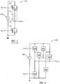
- IGFETs can be connected to provide a switching circuit, such as the switching circuit 100 in FIG. 1 , which allows an output voltage to be at substantially the higher voltage or the lower voltage of a power source 102.
- Two n-channel IGFETs 122 and 124 are connected such that the drain of the IGFET 122 is electrically connected to a positive terminal of the power source 102, and the source of the IGFET 124 is electrically connected to a negative terminal of the power source 102.
- the source of the IGFET 122 and the drain of the IGFET 124 are electrically connected to an output terminal that provides V out .
- the gates of the IGFETs 122 and 124 are electrically connected to input terminals that provide V in1 and V in2 .
- An example of a switching circuit is disclosed in document US 2011/0181255 .
- the input terminals control the switching circuit 100.
- V out will instantaneously be at the voltage of the positive terminal of the power source 102, without any overshoot of the voltage, undershoot of the voltage, or ringing (oscillating between overshoot and undershoot voltages) at the output terminal.
- V out will instantaneously be at the voltage of the negative terminal of the power source 102, without any overshoot of the voltage, undershoot of the voltage, or ringing (oscillating between overshoot and undershoot voltages) at the output terminal.
- the switching circuit 100 is not ideal and has parasitic characteristics between the source of the IGFET 122, the drain of the IGFET 124, and the output terminal V out , even though the three are electrically connected to one another.
- the parasitic characteristics can be modeled as parasitic elements, such as parasitic resistance and parasitic inductance, which are represented within dashed boxes in the figures.
- the parasitic characteristics are modeled with a parasitic resistance 132 and a parasitic inductance 134 connected in series between source of the IGFET 122 and the output terminal.
- the parasitic characteristics can cause ringing at the output node, which can include significant voltage overshoot that can exceed the drain-to-source breakdown voltage of the IGFET 124, damage to a load (not illustrated) coupled to the output terminal, or another adverse effect. It is an object of the invention to mitigate these effects and it is achieved by a circuit as set out in the appended claims.
- Coupled is intended to mean a connection, linking, or association of two or more electronic components, circuits, systems, or any combination of: (1) at least one electronic component, (2) at least one circuit, or (3) at least one system in such a way that a signal (e.g., current, voltage, or optical signal) may be transferred from one to another.
- a signal e.g., current, voltage, or optical signal
- Non-limiting examples of “coupled” can include electrical connections between electronic component(s), circuit(s) or electronic component(s) with switch(es) (e.g., transistor(s)) connected between them, or the like.
- electrically connected with respect to electronic components, circuits, or portions thereof, is intended to mean that two or more electronic components, circuits, or any combination of at least one electronic component and at least one circuit do not have any intervening electronic component lying between them.
- Parasitic resistance, parasitic capacitance, parasitic inductance, or any combination thereof is not considered electronic components for the purposes of this definition.
- electronic components are electrically connected when they are electrically shorted to one another and lie at substantially the same voltage.
- normal operation and "normal operating state” refer to conditions under which an electronic component or device is designed to operate.
- the conditions may be obtained from a data sheet or other information regarding voltages, currents, capacitance, resistance, or other electrical conditions.
- normal operation does not include operating an electrical component or device well beyond its design limits.
- power transistor is intended to mean a transistor that is capable of maintaining at least a 10 V difference between a drain and a source of a field-effect transistor or between a collector and an emitter of a bipolar transistor when the field-effect or bipolar transistor is in an off state.
- a circuit can include a pair of switching elements that have terminals electrically connected to terminals of a power supply and have other terminals electrically connected to an output terminal.
- the circuit can include one or more rectifying elements electrically connected in parallel with a corresponding switching element.
- the circuit can further include one or more charge storage elements electrically connected between the terminals of the power supply.
- the switching elements are transistors, and each transistor has a corresponding rectifying element electrically connected in parallel with the transistor.
- the rectifying element can be a pn junction diode, a Schottky diode, or any combination thereof.
- the storage element can be a capacitor having a parallel plate capacitor structure, a transistor structure, or the like.
- a capacitor is implemented such that the parasitic characteristics between an electrode of the capacitor and one of the terminals of power supply are significantly less than the parasitic characteristics of the other electrode of the capacitor and the other terminal of the power supply.
- the circuit can be a Buck converter. Details regarding the circuits are better understood with respect to particular embodiments as described below, where such embodiments are merely illustrative and do not limit the scope of the present invention.
- FIG. 2 includes a diagram of a circuit 200 in accordance with an embodiment.
- a power supply 202 provides power to the circuit 200 and includes a positive terminal and a negative terminal that is coupled to ground. In another embodiment, more than one power supply may be used or only one of the terminals of the power supply 202 is coupled to the circuit 200. In a further embodiment, the circuit 200 is coupled to terminals of a power supply that has terminals that are not at ground potential.
- the power supply 202 may provide a nominal voltage of 1 V, 5 V, 12 V, 19 V, or another suitable voltage. In a particular embodiment, the power supply 202 is a direct current (DC) power supply.
- the power supply 202 can include a battery, generator, alternator, capacitor, or another suitable device that can provide power to the circuit 202.
- Additional circuitry may be used if needed or desired.
- a bridge rectifier (not illustrated) or another suitable circuit may be used when the power supply 202 is an alternator, and the circuit 200 is to receive a DC voltage instead of an alternating current (AC) voltage.
- the terminals of the power supply 202 are electrically connected to the circuit 200.
- the circuit 200 includes a switching element 222 having a current-carrying terminal coupled to the positive terminal of the power supply 202, and another current-carrying terminal coupled to an output terminal of the circuit 200 that provides V out .
- the circuit 200 includes a switching element 224 having a current-carrying terminal coupled to the negative terminal of the power supply 202, and another current-carrying terminal coupled to the output terminal.
- the switching elements 222 and 224 have control electrodes that are coupled to input terminals for the circuit 200 that provide V in1 and V in2 , respectively to the circuit 200.
- the switching elements 222 and 224 can be field-effect transistors, bipolar transistors, another suitable switching element structure for a switching circuit, or any combination thereof.
- Each of the switching elements 222 and 224 can include a plurality of transistor structures that are connected in parallel, such that the combination of transistor structures is electrically equivalent to a single transistor.
- the circuit 200 further includes rectifying elements 242 and 244.
- the rectifying element 242 has an anode that is coupled to the negative terminal of the power supply 202, and a cathode that is coupled to current-carrying electrodes of the switching elements 222 and 224.
- the rectifying element 244 has an anode that is coupled to current-carrying electrodes of the switching elements 222 and 224, and a cathode that is coupled to the positive terminal of the power supply 202.
- the rectifying elements 242 and 244 can be pn junction diodes, Schottky diodes, another suitable rectifying element structure, or any combination thereof.
- Each of the rectifying elements 242 and 244 can include a plurality of diodes that are connected in parallel, such that the combination of diodes is electrically equivalent to a single diode.
- the circuit 200 still further includes charge storage elements 262 and 264.
- the charge storage element 262 has an electrode that is coupled to the positive terminal of the power supply 202, and another electrode that is coupled to the anode of the rectifying element 242.
- the charge storage element 264 has an electrode that is coupled to the cathode of the rectifying element 244, and another electrode that is coupled to the negative terminal of the power supply 202.
- the charge storage elements 262 and 264 can be in the form of parallel-plate capacitor structures, field-effect transistor structures, another suitable charge storage element structure, or any combination thereof.
- Each of the charge storage elements 262 and 264 can include a plurality of structures that are connected in parallel, such that the combination of structures is electrically equivalent to a single capacitor.
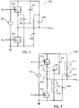
- FIG. 3 includes a diagram of a particular circuit 300 that is a non-limiting implementation of the circuit 200 in accordance with an embodiment.
- the circuit 300 as illustrated in FIG. 3 is a switching circuit, and more particularly is a Buck converter and can be used as a high-frequency voltage regulator.
- the switching elements 222 and 224 in FIG. 2 are n-channel IGFETs 322 and 324 in FIG. 3 .
- the IGFETs 322 and 324 have their bodies tied to their sources.
- the active regions of the IGFETs 322 and 324 form pn junction diodes.
- the pn junction diodes of the IGFETs 322 and 324 can be used to determine maximum sustainable voltage differences that can be maintained across the drains and sources of the IGFETs 322 and 324. Such a voltage difference can be referred to as a drain-to-source breakdown voltage.
- the normal operating voltages of the switching circuit 200 may determine the breakdown voltage in selecting the IGFETs.
- the breakdown voltage may be at least two times the voltage between the terminals of the power supply 202. For example, if the power supply 202 has a nominal voltage of 12 V, the IGFETs 322 and 324 can have a drain-to-source breakdown voltage of at least approximately 24 V.
- the drain-to-source breakdown voltages of the IGFETs 322 and 324 are at least approximately 30 V.
- the IGFETs 322 and 324 may have approximately the same drain-to-source breakdown voltage or different drain-to-source breakdown voltages.
- the rectifying and charge storage elements help to reduce the likelihood that the drain-to-source breakdown of an IGFET does not occur during a transient time after the state of one or both of the IGFETs is changed.
- the rectifying elements 242 and 244 in FIG. 2 are Schottky diodes 342 and 344 in FIG. 3 .
- each of the Schottky diodes 342 and 344 can be replaced by pn diodes, or a combination of pn junction diodes and Schottky diodes.
- the reverse-bias breakdown voltage may be no greater than approximately 2.0 times the drain-to-source breakdown voltage. In a particular embodiment, the reverse-bias breakdown voltage may be no greater than approximately 1.5 times the drain-to-source breakdown voltage, and in a more particular embodiment, the reverse-bias breakdown voltage may be no greater than approximately 1.2 times the drain-to-source breakdown voltage.
- the reverse-bias breakdown voltage may be no greater than approximately 1.0 times the drain-to-source breakdown voltage.
- the Schottky diodes 342 and 344 can have the same reverse-bias breakdown voltage or different reverse-bias breakdown voltages.
- the rectifying element 242, the rectifying element 244, or each of the rectifying elements 242 and 244 can include a plurality of diodes, wherein at least one of the diodes has a reverse-bias breakdown as previously described.
- all diodes within a set of diodes that make up rectifying element 242, rectifying element 244, or each of rectifying elements 242 and 244 can have a reverse-bias breakdown as previously described.
- the charge storage elements 262 and 264 in FIG. 2 are capacitors 362 and 364 in FIG. 3 .
- a ratio of the capacitance of the capacitor 362, capacitor 364, or each of capacitors 362 and 364 to the drain-to-source capacitance of the IGFET 322, the IGFET 324, or each of the IGFETs 322 and 324 can be at least approximately 1.5:1.
- the capacitance of the capacitor 362, capacitor 364, or each of capacitors 362 and 364 to the drain-to-source capacitance can be at least approximately 2:1, and in a more particular embodiment, capacitance of the capacitor 362, capacitor 364, or each of capacitors 362 and 364 to the drain-to-source capacitance can be at least approximately 4:1.
- the capacitance of the capacitor 362, capacitor 364, or each of capacitors 362 and 364 to the drain-to-source capacitance may be no greater than approximately 25:1.
- the capacitance of the capacitor 362, capacitor 364, or each of capacitors 362 and 364 to the drain-to-source capacitance may be no greater than approximately 16:1, and in a more particular embodiment, capacitance of the capacitor 362, capacitor 364, or each of capacitors 362 and 364 to the drain-to-source capacitance may be no greater than approximately 9:1.
- the capacitance of the capacitor 362, capacitor 364, or each of capacitors 362 and 364 can be expressed in absolute, rather than relative, terms. In an embodiment, the capacitance of the capacitor 362, capacitor 364, or each of capacitors 362 and 364 can be at least approximately 80 pF. In a particular embodiment, the capacitance of the capacitor 362, capacitor 364, or each of capacitors 362 and 364 can be at least approximately 200 pF, and in a more particular embodiment, capacitance of the capacitor 362, capacitor 364, or each of capacitors 362 and 364 can be at least approximately 1.5 nF. In another embodiment, the capacitance of the capacitor 362, capacitor 364, or each of capacitors 362 and 364 may be no greater than approximately 40 nF.
- the capacitance of the capacitor 362, capacitor 364, or each of capacitors 362 and 364 may be no greater than approximately 30 nF, and in a more particular embodiment, capacitance of the capacitor 362, capacitor 364, or each of capacitors 362 and 364 may be no greater than approximately 20 nF. In a further embodiment, the capacitance of the capacitor 362, capacitor 364, or each of capacitors 362 and 364 can be in a range of approximately 1.5 nF to approximately 40 nF.
- the output node of the circuit 300 can include the source of the IGFET 322, the drain of IGFET 324, the cathode of the Schottky diode 342, and, the anode of the Schottky diode 344.
- Another node can include the positive terminal of the power supply 202, the drain of the IGFET 322, electrodes of the capacitors 362 and 364, and the cathode of the Schottky diode 344.
- a further node can include the negative terminal of the power supply 202, the source of the IGFET 324, the other electrodes of the capacitors 362 and 364, and the anode of the Schottky diode 342.
- the circuit 300 in FIG. 3 does not take into account parasitic characteristics due to interconnections between the components.
- the IGFETs 322 and 324 may be on different dies and include a metal strap to electrically connect the source of the IGFET 322, the drain of the IGFET 324, and the output terminal to one another. These connections can have parasitic characteristics that can significantly affect the operation of the circuit. The parasitic characteristics can be used when modeling the circuit.
- FIG. 4 includes a circuit 400 that is similar to circuit 300 in FIG. 3 .
- the circuit 400 includes parasitic resistances and parasitic inductances that are illustrated within dashed boxes.
- a parasitic resistor 432 and a parasitic inductor 434 are electrically connected in series between the cathode of the Schottky diode 342 and the output terminal.
- the Schottky diode 342 and capacitor 362 are physically located closer to the IGFET 322 than to the negative terminal of the power supply 202.
- the parasitic characteristics between the negative terminal of the power supply 202 and each of the Schottky diode 342 and the capacitor 362 are more significant than the parasitic characteristics between the IGFET 322 and each of the Schottky diode 342 and the capacitor 362.
- the parasitic characteristics are modeled using a parasitic resistor 452 and a parasitic inductor 454 connected in series between the negative terminal of the power supply 202 and each of the Schottky diode 342 and the capacitor 362.
- the Schottky diode 344 and capacitor 364 are physically located closer to the IGFET 324 than to the positive terminal of the power supply 202.
- the parasitic characteristics between the positive terminal of the power supply 202 and each of the Schottky diode 344 and the capacitor 364 are more significant than the parasitic characteristics between the IGFET 324 and each of the Schottky diode 344 and the capacitor 364.
- the parasitic characteristics are modeled using a parasitic resistor 472 and a parasitic inductor 474 connected in series between the positive terminal of the power supply 202 and each of the Schottky diode 344 and the capacitor 364.
- parasitic resistors in FIGs. 1 and 4 can be assigned a value of less than 1 m ⁇ , and parasitic inductors in FIGs. 1 and 4 can be assigned a value of less than 1 nH.
- the inductance is relatively low, the circuits as described herein, including FIG. 1 , are to operate at frequencies on the order of approximately 1 MHz with significant currents that are over 1000 times greater than typically currents seen with transistors that are used in digital logic circuits, such as memories.
- the circuits as described herein can be used as a high-frequency voltage regulator for a mobile electronic device, such as a laptop computer, a netbook, a table personal computer, or the like.
- the power supply can be a 12 VDC battery.
- the battery may be connected to a charger, and the voltage across the terminals of the power supply can reach as high as 19 V.
- the circuit needs to be able to withstand such a voltage.
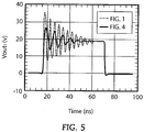
- Example demonstrates that combinations of rectifying elements and charge storage capacitors can be used to reduce ringing at an output terminal of a power switching circuit.
- FIGs. 1 and 4 are used to generate the data for the timing diagram of FIG. 5 .
- the following values are assigned to the parasitic resistances and inductors in FIGs. 1 and 4 :
- FIG. 5 includes a timing diagram that compares the voltage on the output terminal that provides V out as a function of time after a switching event has occurred when the power supply has 19 V across its terminals.
- the IGFET 122 is off, and the IGFET 124 is on.
- the voltage on the output terminal is approximately 0 V.
- the IGFET 124 is turned off, and then, the IGFET 122 is turned on.
- the IGFET 322 is off, and the IGFET 324 is on.
- the voltage on the output terminal is approximately 0 V.
- the IGFET 324 is turned off, and then, the IGFET 322 is turned on.
- the voltage on the output terminal would go from 0 V to 19 V instantaneously with no voltage overshoot, undershoot, or ringing.
- the circuits as illustrated in FIGs. 1 and 4 are not ideal, and therefore, voltage overshoot, voltage undershoot, and ringing occurs.
- the circuit 400 in FIG. 4 provides significantly better performance as compared to circuit 100 in FIG. 1 .
- the capacitors 362 and 364 can quickly charge and allow excess charge to be stored and reduce the amount of voltage overshoot and voltage undershoot.
- the Schottky diodes 342 and 344 help to provide a low impedance current path to the capacitors 362 and 364 during a voltage overshoot or undershoot, while blocking the flow of current when the output terminal is at a voltage equal to or between the voltages on the positive and negative terminals of the power supply. Without the capacitors 362 and 364 and the Schottky diodes 342 and 344, such as circuit 100 in FIG.
- V out can reach 34 V, which exceeds the drain-to-source breakdown voltage of 30 V for the IGFET 124.
- V out can reach 26 V, which is below the drain-to-source breakdown voltage of 30 V for the IGFET 324.
- the ringing seen at the output terminal for the circuit 400 in FIG. 4 is substantially non-existent at least 15 ns sooner than for the output terminal of the circuit 100 in FIG. 1 .
Description
- The present disclosure relates to circuits including switching elements, rectifying elements, and charge storage elements.
- Insulated gate field-effect transistors (IGFETs) are a common type of power switching device. IGFETs can be connected to provide a switching circuit, such as the
switching circuit 100 inFIG. 1 , which allows an output voltage to be at substantially the higher voltage or the lower voltage of apower source 102. Two n-channel IGFETs 122 and 124 are connected such that the drain of the IGFET 122 is electrically connected to a positive terminal of thepower source 102, and the source of the IGFET 124 is electrically connected to a negative terminal of thepower source 102. The source of the IGFET 122 and the drain of the IGFET 124 are electrically connected to an output terminal that provides Vout. The gates of the IGFETs 122 and 124 are electrically connected to input terminals that provide Vin1 and Vin2. An example of a switching circuit is disclosed in documentUS 2011/0181255 . - The input terminals control the
switching circuit 100. Ideally, when the states of the IGFETs 122 and 124 is switched such that the IGFET 122 is on and the IGFET 124 is off, Vout will instantaneously be at the voltage of the positive terminal of thepower source 102, without any overshoot of the voltage, undershoot of the voltage, or ringing (oscillating between overshoot and undershoot voltages) at the output terminal. Ideally, when the states of the IGFETs 122 and 124 is switched such that the IGFET 122 is off and the IGFET 124 is on, Vout will instantaneously be at the voltage of the negative terminal of thepower source 102, without any overshoot of the voltage, undershoot of the voltage, or ringing (oscillating between overshoot and undershoot voltages) at the output terminal. - The
switching circuit 100 is not ideal and has parasitic characteristics between the source of the IGFET 122, the drain of the IGFET 124, and the output terminal Vout, even though the three are electrically connected to one another. The parasitic characteristics can be modeled as parasitic elements, such as parasitic resistance and parasitic inductance, which are represented within dashed boxes in the figures. In theswitching circuit 100, the parasitic characteristics are modeled with aparasitic resistance 132 and aparasitic inductance 134 connected in series between source of the IGFET 122 and the output terminal. As will be discussed later in the specification, the parasitic characteristics can cause ringing at the output node, which can include significant voltage overshoot that can exceed the drain-to-source breakdown voltage of theIGFET 124, damage to a load (not illustrated) coupled to the output terminal, or another adverse effect. It is an object of the invention to mitigate these effects and it is achieved by a circuit as set out in the appended claims. - Embodiments are illustrated by way of example and are not limited in the accompanying figures.
-
FIG. 1 includes a diagram of a switching circuit. (Prior art) -
FIG. 2 includes a diagram of a circuit in accordance with an embodiment. -
FIG. 3 includes a diagram of the circuit inFIG. 2 with particular circuit elements in accordance with a particular embodiment. -
FIG. 4 includes a diagram of the circuit ofFIG. 3 with parasitic characteristics represented with parasitic circuit elements. -
FIG. 5 includes a plot illustrating output voltages of circuits in accordance withFIGs. 1 and4 after the voltage at the output terminal changes from a relatively low voltage to a relatively high voltage. - Skilled artisans appreciate that elements in the figures are illustrated for simplicity and clarity and have not necessarily been drawn to scale. For example, the dimensions of some of the elements in the figures may be exaggerated relative to other elements to help to improve understanding of embodiments of the invention. Also, for conceptual simplicity, some structures that are represented by a single circuit element may in fact correspond to multiple physical elements connected either in series, in parallel, or in some other series and parallel combination.
- The following description in combination with the figures is provided to assist in understanding the teachings disclosed herein. The following discussion will focus on specific implementations and embodiments of the teachings. This focus is provided to assist in describing the teachings and should not be interpreted as a limitation on the scope or applicability of the teachings. However, other teachings can certainly be utilized in this application.
- As used herein, the term "coupled" is intended to mean a connection, linking, or association of two or more electronic components, circuits, systems, or any combination of: (1) at least one electronic component, (2) at least one circuit, or (3) at least one system in such a way that a signal (e.g., current, voltage, or optical signal) may be transferred from one to another. Non-limiting examples of "coupled" can include electrical connections between electronic component(s), circuit(s) or electronic component(s) with switch(es) (e.g., transistor(s)) connected between them, or the like.
- The term "electrically connected," with respect to electronic components, circuits, or portions thereof, is intended to mean that two or more electronic components, circuits, or any combination of at least one electronic component and at least one circuit do not have any intervening electronic component lying between them. Parasitic resistance, parasitic capacitance, parasitic inductance, or any combination thereof is not considered electronic components for the purposes of this definition. In one embodiment, electronic components are electrically connected when they are electrically shorted to one another and lie at substantially the same voltage.
- The term "normal operation" and "normal operating state" refer to conditions under which an electronic component or device is designed to operate. The conditions may be obtained from a data sheet or other information regarding voltages, currents, capacitance, resistance, or other electrical conditions. Thus, normal operation does not include operating an electrical component or device well beyond its design limits.
- The term "power transistor" is intended to mean a transistor that is capable of maintaining at least a 10 V difference between a drain and a source of a field-effect transistor or between a collector and an emitter of a bipolar transistor when the field-effect or bipolar transistor is in an off state.
- The terms "comprises," "comprising," "includes," "including," "has," "having" or any other variation thereof, are intended to cover a non-exclusive inclusion. For example, a method, article, or apparatus that comprises a list of features is not necessarily limited only to those features but may include other features not expressly listed or inherent to such method, article, or apparatus. Further, unless expressly stated to the contrary, "or" refers to an inclusive-or and not to an exclusive-or. For example, a condition A or B is satisfied by any one of the following: A is true (or present) and B is false (or not present), A is false (or not present) and B is true (or present), and both A and B are true (or present).
- Also, the use of "a" or "an" is employed to describe elements and components described herein. This is done merely for convenience and to give a general sense of the scope of the invention. This description should be read to include one or at least one and the singular also includes the plural, or vice versa, unless it is clear that it is meant otherwise. For example, when a single item is described herein, more than one item may be used in place of a single item. Similarly, where more than one item is described herein, a single item may be substituted for that more than one item.
- Unless otherwise defined, all technical and scientific terms used herein have the same meaning as commonly understood by one of ordinary skill in the art to which this invention belongs. The materials, methods, and examples are illustrative only and not intended to be limiting. To the extent not described herein, many details regarding specific materials and processing acts are conventional and may be found in textbooks and other sources within the semiconductor and electronic arts.
- A circuit can include a pair of switching elements that have terminals electrically connected to terminals of a power supply and have other terminals electrically connected to an output terminal. The circuit can include one or more rectifying elements electrically connected in parallel with a corresponding switching element. The circuit can further include one or more charge storage elements electrically connected between the terminals of the power supply. In a particular embodiment, the switching elements are transistors, and each transistor has a corresponding rectifying element electrically connected in parallel with the transistor. The rectifying element can be a pn junction diode, a Schottky diode, or any combination thereof. The storage element can be a capacitor having a parallel plate capacitor structure, a transistor structure, or the like. In a particular embodiment, a capacitor is implemented such that the parasitic characteristics between an electrode of the capacitor and one of the terminals of power supply are significantly less than the parasitic characteristics of the other electrode of the capacitor and the other terminal of the power supply. In a particular embodiment, the circuit can be a Buck converter. Details regarding the circuits are better understood with respect to particular embodiments as described below, where such embodiments are merely illustrative and do not limit the scope of the present invention.
-
FIG. 2 includes a diagram of acircuit 200 in accordance with an embodiment. Apower supply 202 provides power to thecircuit 200 and includes a positive terminal and a negative terminal that is coupled to ground. In another embodiment, more than one power supply may be used or only one of the terminals of thepower supply 202 is coupled to thecircuit 200. In a further embodiment, thecircuit 200 is coupled to terminals of a power supply that has terminals that are not at ground potential. Thepower supply 202 may provide a nominal voltage of 1 V, 5 V, 12 V, 19 V, or another suitable voltage. In a particular embodiment, thepower supply 202 is a direct current (DC) power supply. Thepower supply 202 can include a battery, generator, alternator, capacitor, or another suitable device that can provide power to thecircuit 202. Additional circuitry may be used if needed or desired. For example, a bridge rectifier (not illustrated) or another suitable circuit may be used when thepower supply 202 is an alternator, and thecircuit 200 is to receive a DC voltage instead of an alternating current (AC) voltage. In a particular embodiment, the terminals of thepower supply 202 are electrically connected to thecircuit 200. - The
circuit 200 includes aswitching element 222 having a current-carrying terminal coupled to the positive terminal of thepower supply 202, and another current-carrying terminal coupled to an output terminal of thecircuit 200 that provides Vout. Thecircuit 200 includes aswitching element 224 having a current-carrying terminal coupled to the negative terminal of thepower supply 202, and another current-carrying terminal coupled to the output terminal. The switchingelements circuit 200 that provide Vin1 and Vin2, respectively to thecircuit 200. - The switching
elements elements - The
circuit 200 further includes rectifyingelements element 242 has an anode that is coupled to the negative terminal of thepower supply 202, and a cathode that is coupled to current-carrying electrodes of the switchingelements element 244 has an anode that is coupled to current-carrying electrodes of the switchingelements power supply 202. - The rectifying
elements elements - The
circuit 200 still further includescharge storage elements charge storage element 262 has an electrode that is coupled to the positive terminal of thepower supply 202, and another electrode that is coupled to the anode of the rectifyingelement 242. Thecharge storage element 264 has an electrode that is coupled to the cathode of the rectifyingelement 244, and another electrode that is coupled to the negative terminal of thepower supply 202. - The
charge storage elements charge storage elements -
FIG. 3 includes a diagram of aparticular circuit 300 that is a non-limiting implementation of thecircuit 200 in accordance with an embodiment. Thecircuit 300 as illustrated inFIG. 3 is a switching circuit, and more particularly is a Buck converter and can be used as a high-frequency voltage regulator. The switchingelements FIG. 2 are n-channel IGFETs FIG. 3 . TheIGFETs - The active regions of the
IGFETs IGFETs IGFETs switching circuit 200 may determine the breakdown voltage in selecting the IGFETs. The breakdown voltage may be at least two times the voltage between the terminals of thepower supply 202. For example, if thepower supply 202 has a nominal voltage of 12 V, theIGFETs IGFETs IGFETs - The rectifying
elements FIG. 2 areSchottky diodes FIG. 3 . In another embodiment, each of theSchottky diodes Schottky diodes element 242, the rectifyingelement 244, or each of the rectifyingelements element 242, rectifyingelement 244, or each of rectifyingelements - The
charge storage elements FIG. 2 arecapacitors FIG. 3 . A ratio of the capacitance of thecapacitor 362,capacitor 364, or each ofcapacitors IGFET 322, theIGFET 324, or each of theIGFETs capacitor 362,capacitor 364, or each ofcapacitors capacitor 362,capacitor 364, or each ofcapacitors capacitor 362,capacitor 364, or each ofcapacitors capacitor 362,capacitor 364, or each ofcapacitors capacitor 362,capacitor 364, or each ofcapacitors - The capacitance of the
capacitor 362,capacitor 364, or each ofcapacitors capacitor 362,capacitor 364, or each ofcapacitors capacitor 362,capacitor 364, or each ofcapacitors capacitor 362,capacitor 364, or each ofcapacitors capacitor 362,capacitor 364, or each ofcapacitors capacitor 362,capacitor 364, or each ofcapacitors capacitor 362,capacitor 364, or each ofcapacitors capacitor 362,capacitor 364, or each ofcapacitors - Many values have been provided for the electronic elements within the
circuits - In the circuits as described in 200 and 300 in
FIGs. 2 and3 , the couplings between circuit elements can be electrical connections. With respect toFIG. 3 , the output node of thecircuit 300 can include the source of theIGFET 322, the drain ofIGFET 324, the cathode of theSchottky diode 342, and, the anode of theSchottky diode 344. Another node can include the positive terminal of thepower supply 202, the drain of theIGFET 322, electrodes of thecapacitors Schottky diode 344. A further node can include the negative terminal of thepower supply 202, the source of theIGFET 324, the other electrodes of thecapacitors Schottky diode 342. - The
circuit 300 inFIG. 3 does not take into account parasitic characteristics due to interconnections between the components. For example, theIGFETs IGFET 322, the drain of theIGFET 324, and the output terminal to one another. These connections can have parasitic characteristics that can significantly affect the operation of the circuit. The parasitic characteristics can be used when modeling the circuit. -
FIG. 4 includes acircuit 400 that is similar tocircuit 300 inFIG. 3 . Thecircuit 400 includes parasitic resistances and parasitic inductances that are illustrated within dashed boxes. Aparasitic resistor 432 and aparasitic inductor 434 are electrically connected in series between the cathode of theSchottky diode 342 and the output terminal. TheSchottky diode 342 andcapacitor 362 are physically located closer to theIGFET 322 than to the negative terminal of thepower supply 202. The parasitic characteristics between the negative terminal of thepower supply 202 and each of theSchottky diode 342 and thecapacitor 362 are more significant than the parasitic characteristics between theIGFET 322 and each of theSchottky diode 342 and thecapacitor 362. Thus, the parasitic characteristics are modeled using aparasitic resistor 452 and aparasitic inductor 454 connected in series between the negative terminal of thepower supply 202 and each of theSchottky diode 342 and thecapacitor 362. TheSchottky diode 344 andcapacitor 364 are physically located closer to theIGFET 324 than to the positive terminal of thepower supply 202. The parasitic characteristics between the positive terminal of thepower supply 202 and each of theSchottky diode 344 and thecapacitor 364 are more significant than the parasitic characteristics between theIGFET 324 and each of theSchottky diode 344 and thecapacitor 364. Thus, the parasitic characteristics are modeled using aparasitic resistor 472 and a parasitic inductor 474 connected in series between the positive terminal of thepower supply 202 and each of theSchottky diode 344 and thecapacitor 364. - For modeling purposes, parasitic resistors in
FIGs. 1 and4 can be assigned a value of less than 1 mΩ, and parasitic inductors inFIGs. 1 and4 can be assigned a value of less than 1 nH. Although the inductance is relatively low, the circuits as described herein, includingFIG. 1 , are to operate at frequencies on the order of approximately 1 MHz with significant currents that are over 1000 times greater than typically currents seen with transistors that are used in digital logic circuits, such as memories. The relationship between voltage and inductance is V = L*(di/dt), and therefore, a very large value for di/dt can cause ringing as will be seen for the circuit ofFIG. 1 . - The circuits as described herein can be used as a high-frequency voltage regulator for a mobile electronic device, such as a laptop computer, a netbook, a table personal computer, or the like. In a non-limiting embodiment, the power supply can be a 12 VDC battery. During normal operation of the mobile electronic device, the battery may be connected to a charger, and the voltage across the terminals of the power supply can reach as high as 19 V. Thus, the circuit needs to be able to withstand such a voltage.
- The concepts described herein will be further described in the Example, which does not limit the scope of the invention described in the claims. The Example demonstrates that combinations of rectifying elements and charge storage capacitors can be used to reduce ringing at an output terminal of a power switching circuit.
- The circuits of
FIGs. 1 and4 are used to generate the data for the timing diagram ofFIG. 5 . The following values are assigned to the parasitic resistances and inductors inFIGs. 1 and4 : -
Parasitic resistor 132, 250 µΩ; -
Parasitic inductor -
Parasitic resistor 432, 250 µΩ; -
Parasitic inductor -
Parasitic resistor 452, 25 mΩ; -
Parasitic inductor 454, 150 pH; -
Parasitic resistor 472, 50 mΩ; and - Parasitic inductor 474, 250 pH.
-
FIG. 5 includes a timing diagram that compares the voltage on the output terminal that provides Vout as a function of time after a switching event has occurred when the power supply has 19 V across its terminals. At t=0, theIGFET 122 is off, and theIGFET 124 is on. The voltage on the output terminal is approximately 0 V. At approximately t=15 ns, theIGFET 124 is turned off, and then, theIGFET 122 is turned on. At t=0, theIGFET 322 is off, and theIGFET 324 is on. The voltage on the output terminal is approximately 0 V. At approximately t=15 ns, theIGFET 324 is turned off, and then, theIGFET 322 is turned on. Ideally, the voltage on the output terminal would go from 0 V to 19 V instantaneously with no voltage overshoot, undershoot, or ringing. The circuits as illustrated inFIGs. 1 and4 are not ideal, and therefore, voltage overshoot, voltage undershoot, and ringing occurs. - Clearly, the
circuit 400 inFIG. 4 provides significantly better performance as compared tocircuit 100 inFIG. 1 . Thecapacitors Schottky diodes capacitors capacitors Schottky diodes circuit 100 inFIG. 1 , Vout can reach 34 V, which exceeds the drain-to-source breakdown voltage of 30 V for theIGFET 124. With thecapacitors Schottky diodes circuit 400 inFIG. 4 , Vout can reach 26 V, which is below the drain-to-source breakdown voltage of 30 V for theIGFET 324. Further, the ringing seen at the output terminal for thecircuit 400 inFIG. 4 is substantially non-existent at least 15 ns sooner than for the output terminal of thecircuit 100 inFIG. 1 . - Note that not all of the activities described above in the general description or the examples are required, that a portion of a specific activity may not be required, and that one or more further activities may be performed in addition to those described. Still further, the order in which activities are listed is not necessarily the order in which they are performed.
- Benefits, other advantages, and solutions to problems have been described above with regard to specific embodiments. However, the benefits, advantages, solutions to problems, and any feature(s) that may cause any benefit, advantage, or solution to occur or become more pronounced are not to be construed as a critical, required, or essential feature of any or all the claims.
- The specification and illustrations of the embodiments described herein are intended to provide a general understanding of the structure of the various embodiments. The specification and illustrations are not intended to serve as an exhaustive and comprehensive description of all of the elements and features of apparatus and systems that use the structures or methods described herein. Certain features are, for clarity, described herein in the context of separate embodiments, may also be provided in combination in a single embodiment. Conversely, various features that are, for brevity, described in the context of a single embodiment, may also be provided separately or in any subcombination. Further, reference to values stated in ranges includes each and every value within that range. Many other embodiments may be apparent to skilled artisans only after reading this specification. Accordingly, the disclosure is to be regarded as illustrative rather than restrictive.
Claims (9)
- A circuit (400) comprising:a power supply (202) having a positive supply terminal and a negative supply terminal;a first switching element (322) having a first current-carrying electrode and a second current-carrying electrode, wherein the first current-carrying electrode is coupled to the positive supply terminal;a second switching element (324) having a first current-carrying electrode and a second current-carrying electrode, wherein the first current-carrying electrode of the second switching element (324) is coupled to the second current-carrying electrode of the first switching element (322) and the second current-carrying electrode of the second switching element (324) is coupled to the negative supply terminal;a first rectifying element (344) having an anode and a cathode, wherein the anode of the first rectifying element (344) is coupled to the second current-carrying electrode of the first switching element (322), and the cathode of the first rectifying element (344) is coupled to the first current-carrying electrode of the first switching element (322);a second rectifying element (342) having an anode and a cathode, wherein the anode of the second rectifying element (342) is coupled to the second current-carrying electrode of the second switching element (324), and the cathode of the second rectifying element (342) is coupled to the first current-carrying electrode of the second switching element (324);a first charge storage element (364) having a first terminal and a second terminal, wherein the first terminal of the first charge storage element (364) is coupled to the cathode of the first rectifying element (344), and the second terminal of the first charge storage element (364) is coupled to the second current-carrying electrode of the second switching element (324); and a second charge storage element (362) having a first terminal and a second terminal, wherein the first terminal of the second charge storage element (362) is coupled to the first current-carrying electrode of the first switching element (322), and wherein the second terminal of the second charge storage element (362) is coupled to the anode of the second rectifying element (342); characterised in that the first rectifying element (344) and the first charge storage element (364) are physically located closer to the second switching element (324) than to the positive supply terminal of the power supply (202); andthe second rectifying element (342) and the second charge storage element (362) are physically located closer to the first switching element (322) than to the negative supply terminal of the power supply (202).
- The circuit of claim 1, wherein the first charge storage element (364), the second charge storage element (362), or each of the first and second charge storage elements includes a capacitor.
- The circuit of claim 1 or 2, wherein the first charge storage element (364), the second charge storage element (362), or each of the first and second charge storage elements has a capacitance of at least 80 pF, or more particularly, in a range of 1.5 nF to 40 nF.
- The circuit of claim 1 or 2, wherein the first charge storage element (364), the second charge storage element (362), or each of the first and second charge storage elements has a particular capacitance; the first switching element (322), the second switching element (324) or each of the first and second switching elements has capacitance between its corresponding first and second current-carrying electrodes, and a ratio of the particular capacitance to the capacitance between its corresponding first and second current-carrying electrodes is at least 1.5:1.
- The circuit of any preceding claim, wherein the first rectifying element (344), the second rectifying element (342), or each of the first and second rectifying elements includes a Schottky diode or a pn junction diode.
- The circuit of any preceding claim, wherein:
the first rectifying element (344), the second rectifying element (342), or each of the first and second rectifying elements includes a Schottky diode and a pn junction diode that are electrically connected in parallel. - The circuit of any preceding claim, wherein:the first rectifying element (344) has a breakdown voltage that is no greater than 2.0 times a drain-to-source breakdown voltage of the first switching element (322); andthe second rectifying element (342) has a breakdown voltage that is no greater than 2.0 times a drain-to-source breakdown voltage of the second switching element (324).
- The circuit of any preceding claim, wherein:the first switching element (322) is an insulated gate field-effect transistor that includes a gate, wherein the first current-carrying electrode of the first switching element is a drain, and the second current-carrying electrode of the first switching element is a source; andthe second switching element (324) is another insulated gate field-effect transistor that includes a gate, wherein the first current-carrying electrode of the second switching element is a drain, and the second current-carrying electrode of the second switching element is a source.
- The circuit of any preceding claim, wherein the circuit is a switching circuit of a voltage regulator.
Applications Claiming Priority (1)
| Application Number | Priority Date | Filing Date | Title |
|---|---|---|---|
| US13/794,038 US9070562B2 (en) | 2013-03-11 | 2013-03-11 | Circuit including a switching element, a rectifying element, and a charge storage element |
Publications (2)
| Publication Number | Publication Date |
|---|---|
| EP2779453A1 EP2779453A1 (en) | 2014-09-17 |
| EP2779453B1 true EP2779453B1 (en) | 2018-08-22 |
Family
ID=50190353
Family Applications (1)
| Application Number | Title | Priority Date | Filing Date |
|---|---|---|---|
| EP14157818.7A Active EP2779453B1 (en) | 2013-03-11 | 2014-03-05 | Circuit including a Switching Element, a Rectifying Element, and a Charge Storage Element |
Country Status (6)
| Country | Link |
|---|---|
| US (1) | US9070562B2 (en) |
| EP (1) | EP2779453B1 (en) |
| JP (1) | JP6300349B2 (en) |
| KR (1) | KR102121719B1 (en) |
| CN (1) | CN203911749U (en) |
| TW (1) | TWI601380B (en) |
Families Citing this family (6)
| Publication number | Priority date | Publication date | Assignee | Title |
|---|---|---|---|---|
| CN106469976B (en) * | 2015-08-20 | 2019-03-15 | 台达电子工业股份有限公司 | Converter and voltage clamp unit |
| US10153213B2 (en) | 2015-08-27 | 2018-12-11 | Semiconductor Components Industries, Llc | Process of forming an electronic device including a drift region, a sinker region and a resurf region |
| US20170062410A1 (en) * | 2015-08-31 | 2017-03-02 | Semiconductor Components Industries, Llc | Circuit including a rectifying element, an electronic device including a diode and a process of forming the same |
| US9680381B1 (en) | 2016-01-29 | 2017-06-13 | Semiconductor Components Industries, Llc | Circuit including rectifying elements and a charge storage element and a method of using an electronic device including a circuit having switching elements |
| US10291052B2 (en) * | 2016-05-25 | 2019-05-14 | Fairchild Semiconductor Corporation | Bypass charging circuit and method |
| US10116303B2 (en) | 2016-07-01 | 2018-10-30 | Toyota Motor Engineering & Manufacturing North America, Inc. | Parallel devices having balanced switching current and power |
Citations (1)
| Publication number | Priority date | Publication date | Assignee | Title |
|---|---|---|---|---|
| US20110181255A1 (en) * | 2010-01-25 | 2011-07-28 | Renesas Electronics Corporation | Semiconductor device and power supply unit using the same |
Family Cites Families (33)
| Publication number | Priority date | Publication date | Assignee | Title |
|---|---|---|---|---|
| JPS58202623A (en) * | 1982-05-21 | 1983-11-25 | Hitachi Ltd | Transistor switch circuit |
| US5966003A (en) * | 1997-05-15 | 1999-10-12 | Fujitsu Limited | DC-DC converter control circuit |
| US6617642B1 (en) | 2000-02-23 | 2003-09-09 | Tripath Technology, Inc. | Field effect transistor structure for driving inductive loads |
| JP4051875B2 (en) * | 2000-10-31 | 2008-02-27 | 富士電機ホールディングス株式会社 | Rectifier circuit and control method thereof |
| JP2002217416A (en) | 2001-01-16 | 2002-08-02 | Hitachi Ltd | Semiconductor device |
| JP2002290224A (en) | 2001-03-23 | 2002-10-04 | Tdk Corp | Semiconductor element |
| US6867553B2 (en) * | 2003-04-16 | 2005-03-15 | General Electric Company | Continuous mode voltage fed inverter |
| US6940189B2 (en) * | 2003-07-31 | 2005-09-06 | Andrew Roman Gizara | System and method for integrating a digital core with a switch mode power supply |
| JP4565879B2 (en) * | 2004-04-19 | 2010-10-20 | ルネサスエレクトロニクス株式会社 | Semiconductor device |
| JP2006049341A (en) | 2004-07-30 | 2006-02-16 | Renesas Technology Corp | Semiconductor device and manufacturing method thereof |
| JP4075884B2 (en) * | 2004-11-05 | 2008-04-16 | 株式会社デンソー | Power control circuit for charge storage element |
| US7462897B2 (en) * | 2005-01-31 | 2008-12-09 | Semiconductor Energy Laboratory Co., Ltd. | Light emitting device and electronic device |
| WO2007048196A1 (en) | 2005-10-26 | 2007-05-03 | Sf2 Infrastructure Limited | Mosfet circuits |
| US7495877B2 (en) * | 2006-03-26 | 2009-02-24 | Alpha & Omega Semiconductor, Ltd. | Circuit configuration and method to reduce ringing in the semiconductor power switching circuits |
| JP5186095B2 (en) * | 2006-10-02 | 2013-04-17 | 株式会社日立製作所 | Gate drive circuit |
| TW200820166A (en) * | 2006-10-27 | 2008-05-01 | Beyond Innovation Tech Co Ltd | Driving device and switching circuit thereof |
| US8427235B2 (en) * | 2007-04-13 | 2013-04-23 | Advanced Analogic Technologies, Inc. | Power-MOSFETs with improved efficiency for multi-channel class-D audio amplifiers and packaging thereof |
| JP2009159184A (en) * | 2007-12-26 | 2009-07-16 | Hitachi Ltd | Circuit device having freewheel diode, circuit device using diode, and electric power converter using the circuit device |
| JP4557015B2 (en) * | 2008-02-15 | 2010-10-06 | 株式会社デンソー | Power switching circuit |
| US8026704B2 (en) * | 2008-06-06 | 2011-09-27 | Infineon Technologies Austria Ag | System and method for controlling a converter |
| JP5217849B2 (en) * | 2008-09-29 | 2013-06-19 | サンケン電気株式会社 | Electrical circuit switching device |
| US8222695B2 (en) | 2009-06-30 | 2012-07-17 | Semiconductor Components Industries, Llc | Process of forming an electronic device including an integrated circuit with transistors coupled to each other |
| TW201105015A (en) * | 2009-07-22 | 2011-02-01 | Green Solution Tech Co Ltd | Charge pump circuit |
| US20110156682A1 (en) | 2009-12-30 | 2011-06-30 | Dev Alok Girdhar | Voltage converter with integrated schottky device and systems including same |
| US8299560B2 (en) | 2010-02-08 | 2012-10-30 | Semiconductor Components Industries, Llc | Electronic device including a buried insulating layer and a vertical conductive structure extending therethrough and a process of forming the same |
| JP5525917B2 (en) * | 2010-05-27 | 2014-06-18 | ローム株式会社 | Electronic circuit |
| JP2012005249A (en) * | 2010-06-17 | 2012-01-05 | Sanken Electric Co Ltd | Switching power supply circuit |
| JP5568645B2 (en) * | 2010-12-01 | 2014-08-06 | 株式会社安川電機 | Power converter |
| US9166028B2 (en) * | 2011-05-31 | 2015-10-20 | Infineon Technologies Austria Ag | Circuit configured to adjust the activation state of transistors based on load conditions |
| JP5727300B2 (en) * | 2011-05-31 | 2015-06-03 | トランスフォーム・ジャパン株式会社 | Voltage regulator |
| US8570005B2 (en) * | 2011-09-12 | 2013-10-29 | Solaredge Technologies Ltd. | Direct current link circuit |
| JP5420711B2 (en) * | 2012-04-18 | 2014-02-19 | 株式会社日立製作所 | Circuit device with freewheeling diode |
| US9192424B2 (en) * | 2012-05-31 | 2015-11-24 | Covidien Lp | AC active load |
-
2013
- 2013-03-11 US US13/794,038 patent/US9070562B2/en active Active
-
2014
- 2014-02-05 TW TW103103832A patent/TWI601380B/en active
- 2014-02-06 JP JP2014021259A patent/JP6300349B2/en active Active
- 2014-02-26 CN CN201420082316.5U patent/CN203911749U/en not_active Expired - Fee Related
- 2014-02-28 KR KR1020140023999A patent/KR102121719B1/en active IP Right Grant
- 2014-03-05 EP EP14157818.7A patent/EP2779453B1/en active Active
Patent Citations (1)
| Publication number | Priority date | Publication date | Assignee | Title |
|---|---|---|---|---|
| US20110181255A1 (en) * | 2010-01-25 | 2011-07-28 | Renesas Electronics Corporation | Semiconductor device and power supply unit using the same |
Also Published As
| Publication number | Publication date |
|---|---|
| KR102121719B1 (en) | 2020-06-11 |
| JP2014176290A (en) | 2014-09-22 |
| KR20140111594A (en) | 2014-09-19 |
| US9070562B2 (en) | 2015-06-30 |
| CN203911749U (en) | 2014-10-29 |
| EP2779453A1 (en) | 2014-09-17 |
| TW201503584A (en) | 2015-01-16 |
| TWI601380B (en) | 2017-10-01 |
| JP6300349B2 (en) | 2018-03-28 |
| US20140252409A1 (en) | 2014-09-11 |
Similar Documents
| Publication | Publication Date | Title |
|---|---|---|
| EP2779453B1 (en) | Circuit including a Switching Element, a Rectifying Element, and a Charge Storage Element | |
| US9172365B2 (en) | Method and circuit for controlling turnoff of a semiconductor switching element | |
| US20160190921A1 (en) | Selectable-mode voltage regulator topology | |
| US20150311792A1 (en) | Switched reference mosfet drive assist circuit | |
| WO2016002249A1 (en) | Switching circuit and power supply circuit provided therewith | |
| JP2015511112A (en) | System and apparatus for driver circuit for protection of GaN FET gate | |
| EP2517343A2 (en) | Stacked nmos dc-to-dc power conversion | |
| US10075079B2 (en) | Driver for low emission switching regulator | |
| US20150077082A1 (en) | Apparatus and Method for a Boost Converter with Improved Electrical Overstress (EOS) Tolerance | |
| US20170179825A1 (en) | Switched mode power supply converter | |
| US11205957B2 (en) | Boost converter | |
| US20180123585A1 (en) | Power device for high voltage and high current switching | |
| US9966846B2 (en) | Circuit including dual power converters and an inductor and a method of using an electronic device including a circuit including dual power converters and an inductor | |
| US11527951B2 (en) | Reverse X2 mode charge pump soft start | |
| Mu et al. | Floating-Domain Integrated GaN Driver Techniques for DC–DC Converters: A Review | |
| US9853636B2 (en) | Semiconductor apparatus | |
| US9680381B1 (en) | Circuit including rectifying elements and a charge storage element and a method of using an electronic device including a circuit having switching elements | |
| US20150200586A1 (en) | Boost DC-DC Converter with Inrush Current Protection Device and Inrush Current Protecting Method | |
| Ahn et al. | A study on zcs problem due to phase change in inductive power transfer charging system applying gan fet | |
| US10447138B2 (en) | Converter configured to convert a DC input voltage to a DC output voltage and including at least one resistive element | |
| US9515571B2 (en) | Current-rectifying device, gate-boosting rectifier and method of permitting current to flow in one direction when driven by AC input voltage | |
| Singh et al. | Body Connection Assessment of MOS-Diodes for MOS-Quadrupler based RF Energy Harvesting Circuit | |
| Sanjeev et al. | Some practical considerations of RF to DC converter using low Vth CMOS rectifier | |
| WO2023070308A1 (en) | Power supply and a method performed by a power supply | |
| Sern Mi Lim et al. | An optimal power management circuit with a dynamic subthreshold start‐up for thermal energy harvesting |
Legal Events
| Date | Code | Title | Description |
|---|---|---|---|
| 17P | Request for examination filed |
Effective date: 20140305 |
|
| AK | Designated contracting states |
Kind code of ref document: A1 Designated state(s): AL AT BE BG CH CY CZ DE DK EE ES FI FR GB GR HR HU IE IS IT LI LT LU LV MC MK MT NL NO PL PT RO RS SE SI SK SM TR |
|
| AX | Request for extension of the european patent |
Extension state: BA ME |
|
| PUAI | Public reference made under article 153(3) epc to a published international application that has entered the european phase |
Free format text: ORIGINAL CODE: 0009012 |
|
| R17P | Request for examination filed (corrected) |
Effective date: 20150316 |
|
| RBV | Designated contracting states (corrected) |
Designated state(s): AL AT BE BG CH CY CZ DE DK EE ES FI FR GB GR HR HU IE IS IT LI LT LU LV MC MK MT NL NO PL PT RO RS SE SI SK SM TR |
|
| 17Q | First examination report despatched |
Effective date: 20160512 |
|
| STAA | Information on the status of an ep patent application or granted ep patent |
Free format text: STATUS: EXAMINATION IS IN PROGRESS |
|
| GRAP | Despatch of communication of intention to grant a patent |
Free format text: ORIGINAL CODE: EPIDOSNIGR1 |
|
| STAA | Information on the status of an ep patent application or granted ep patent |
Free format text: STATUS: GRANT OF PATENT IS INTENDED |
|
| INTG | Intention to grant announced |
Effective date: 20180302 |
|
| GRAS | Grant fee paid |
Free format text: ORIGINAL CODE: EPIDOSNIGR3 |
|
| GRAA | (expected) grant |
Free format text: ORIGINAL CODE: 0009210 |
|
| STAA | Information on the status of an ep patent application or granted ep patent |
Free format text: STATUS: THE PATENT HAS BEEN GRANTED |
|
| AK | Designated contracting states |
Kind code of ref document: B1 Designated state(s): AL AT BE BG CH CY CZ DE DK EE ES FI FR GB GR HR HU IE IS IT LI LT LU LV MC MK MT NL NO PL PT RO RS SE SI SK SM TR |
|
| REG | Reference to a national code |
Ref country code: GB Ref legal event code: FG4D |
|
| REG | Reference to a national code |
Ref country code: CH Ref legal event code: EP |
|
| REG | Reference to a national code |
Ref country code: AT Ref legal event code: REF Ref document number: 1033648 Country of ref document: AT Kind code of ref document: T Effective date: 20180915 |
|
| REG | Reference to a national code |
Ref country code: IE Ref legal event code: FG4D |
|
| REG | Reference to a national code |
Ref country code: DE Ref legal event code: R096 Ref document number: 602014030718 Country of ref document: DE |
|
| REG | Reference to a national code |
Ref country code: NL Ref legal event code: FP |
|
| REG | Reference to a national code |
Ref country code: LT Ref legal event code: MG4D |
|
| PG25 | Lapsed in a contracting state [announced via postgrant information from national office to epo] |
Ref country code: LT Free format text: LAPSE BECAUSE OF FAILURE TO SUBMIT A TRANSLATION OF THE DESCRIPTION OR TO PAY THE FEE WITHIN THE PRESCRIBED TIME-LIMIT Effective date: 20180822 Ref country code: BG Free format text: LAPSE BECAUSE OF FAILURE TO SUBMIT A TRANSLATION OF THE DESCRIPTION OR TO PAY THE FEE WITHIN THE PRESCRIBED TIME-LIMIT Effective date: 20181122 Ref country code: SE Free format text: LAPSE BECAUSE OF FAILURE TO SUBMIT A TRANSLATION OF THE DESCRIPTION OR TO PAY THE FEE WITHIN THE PRESCRIBED TIME-LIMIT Effective date: 20180822 Ref country code: GR Free format text: LAPSE BECAUSE OF FAILURE TO SUBMIT A TRANSLATION OF THE DESCRIPTION OR TO PAY THE FEE WITHIN THE PRESCRIBED TIME-LIMIT Effective date: 20181123 Ref country code: RS Free format text: LAPSE BECAUSE OF FAILURE TO SUBMIT A TRANSLATION OF THE DESCRIPTION OR TO PAY THE FEE WITHIN THE PRESCRIBED TIME-LIMIT Effective date: 20180822 Ref country code: NO Free format text: LAPSE BECAUSE OF FAILURE TO SUBMIT A TRANSLATION OF THE DESCRIPTION OR TO PAY THE FEE WITHIN THE PRESCRIBED TIME-LIMIT Effective date: 20181122 Ref country code: IS Free format text: LAPSE BECAUSE OF FAILURE TO SUBMIT A TRANSLATION OF THE DESCRIPTION OR TO PAY THE FEE WITHIN THE PRESCRIBED TIME-LIMIT Effective date: 20181222 Ref country code: FI Free format text: LAPSE BECAUSE OF FAILURE TO SUBMIT A TRANSLATION OF THE DESCRIPTION OR TO PAY THE FEE WITHIN THE PRESCRIBED TIME-LIMIT Effective date: 20180822 |
|
| REG | Reference to a national code |
Ref country code: AT Ref legal event code: MK05 Ref document number: 1033648 Country of ref document: AT Kind code of ref document: T Effective date: 20180822 |
|
| PG25 | Lapsed in a contracting state [announced via postgrant information from national office to epo] |
Ref country code: LV Free format text: LAPSE BECAUSE OF FAILURE TO SUBMIT A TRANSLATION OF THE DESCRIPTION OR TO PAY THE FEE WITHIN THE PRESCRIBED TIME-LIMIT Effective date: 20180822 Ref country code: AL Free format text: LAPSE BECAUSE OF FAILURE TO SUBMIT A TRANSLATION OF THE DESCRIPTION OR TO PAY THE FEE WITHIN THE PRESCRIBED TIME-LIMIT Effective date: 20180822 Ref country code: HR Free format text: LAPSE BECAUSE OF FAILURE TO SUBMIT A TRANSLATION OF THE DESCRIPTION OR TO PAY THE FEE WITHIN THE PRESCRIBED TIME-LIMIT Effective date: 20180822 |
|
| PG25 | Lapsed in a contracting state [announced via postgrant information from national office to epo] |
Ref country code: ES Free format text: LAPSE BECAUSE OF FAILURE TO SUBMIT A TRANSLATION OF THE DESCRIPTION OR TO PAY THE FEE WITHIN THE PRESCRIBED TIME-LIMIT Effective date: 20180822 Ref country code: AT Free format text: LAPSE BECAUSE OF FAILURE TO SUBMIT A TRANSLATION OF THE DESCRIPTION OR TO PAY THE FEE WITHIN THE PRESCRIBED TIME-LIMIT Effective date: 20180822 Ref country code: PL Free format text: LAPSE BECAUSE OF FAILURE TO SUBMIT A TRANSLATION OF THE DESCRIPTION OR TO PAY THE FEE WITHIN THE PRESCRIBED TIME-LIMIT Effective date: 20180822 Ref country code: IT Free format text: LAPSE BECAUSE OF FAILURE TO SUBMIT A TRANSLATION OF THE DESCRIPTION OR TO PAY THE FEE WITHIN THE PRESCRIBED TIME-LIMIT Effective date: 20180822 Ref country code: EE Free format text: LAPSE BECAUSE OF FAILURE TO SUBMIT A TRANSLATION OF THE DESCRIPTION OR TO PAY THE FEE WITHIN THE PRESCRIBED TIME-LIMIT Effective date: 20180822 Ref country code: CZ Free format text: LAPSE BECAUSE OF FAILURE TO SUBMIT A TRANSLATION OF THE DESCRIPTION OR TO PAY THE FEE WITHIN THE PRESCRIBED TIME-LIMIT Effective date: 20180822 Ref country code: RO Free format text: LAPSE BECAUSE OF FAILURE TO SUBMIT A TRANSLATION OF THE DESCRIPTION OR TO PAY THE FEE WITHIN THE PRESCRIBED TIME-LIMIT Effective date: 20180822 |
|
| REG | Reference to a national code |
Ref country code: DE Ref legal event code: R097 Ref document number: 602014030718 Country of ref document: DE |
|
| PG25 | Lapsed in a contracting state [announced via postgrant information from national office to epo] |
Ref country code: DK Free format text: LAPSE BECAUSE OF FAILURE TO SUBMIT A TRANSLATION OF THE DESCRIPTION OR TO PAY THE FEE WITHIN THE PRESCRIBED TIME-LIMIT Effective date: 20180822 Ref country code: SM Free format text: LAPSE BECAUSE OF FAILURE TO SUBMIT A TRANSLATION OF THE DESCRIPTION OR TO PAY THE FEE WITHIN THE PRESCRIBED TIME-LIMIT Effective date: 20180822 Ref country code: SK Free format text: LAPSE BECAUSE OF FAILURE TO SUBMIT A TRANSLATION OF THE DESCRIPTION OR TO PAY THE FEE WITHIN THE PRESCRIBED TIME-LIMIT Effective date: 20180822 |
|
| PLBE | No opposition filed within time limit |
Free format text: ORIGINAL CODE: 0009261 |
|
| STAA | Information on the status of an ep patent application or granted ep patent |
Free format text: STATUS: NO OPPOSITION FILED WITHIN TIME LIMIT |
|
| 26N | No opposition filed |
Effective date: 20190523 |
|
| PG25 | Lapsed in a contracting state [announced via postgrant information from national office to epo] |
Ref country code: SI Free format text: LAPSE BECAUSE OF FAILURE TO SUBMIT A TRANSLATION OF THE DESCRIPTION OR TO PAY THE FEE WITHIN THE PRESCRIBED TIME-LIMIT Effective date: 20180822 |
|
| PG25 | Lapsed in a contracting state [announced via postgrant information from national office to epo] |
Ref country code: MC Free format text: LAPSE BECAUSE OF FAILURE TO SUBMIT A TRANSLATION OF THE DESCRIPTION OR TO PAY THE FEE WITHIN THE PRESCRIBED TIME-LIMIT Effective date: 20180822 |
|
| REG | Reference to a national code |
Ref country code: CH Ref legal event code: PL |
|
| GBPC | Gb: european patent ceased through non-payment of renewal fee |
Effective date: 20190305 |
|
| PG25 | Lapsed in a contracting state [announced via postgrant information from national office to epo] |
Ref country code: LU Free format text: LAPSE BECAUSE OF NON-PAYMENT OF DUE FEES Effective date: 20190305 |
|
| REG | Reference to a national code |
Ref country code: BE Ref legal event code: MM Effective date: 20190331 |
|
| PG25 | Lapsed in a contracting state [announced via postgrant information from national office to epo] |
Ref country code: IE Free format text: LAPSE BECAUSE OF NON-PAYMENT OF DUE FEES Effective date: 20190305 Ref country code: GB Free format text: LAPSE BECAUSE OF NON-PAYMENT OF DUE FEES Effective date: 20190305 Ref country code: CH Free format text: LAPSE BECAUSE OF NON-PAYMENT OF DUE FEES Effective date: 20190331 Ref country code: LI Free format text: LAPSE BECAUSE OF NON-PAYMENT OF DUE FEES Effective date: 20190331 |
|
| PG25 | Lapsed in a contracting state [announced via postgrant information from national office to epo] |
Ref country code: BE Free format text: LAPSE BECAUSE OF NON-PAYMENT OF DUE FEES Effective date: 20190331 |
|
| PG25 | Lapsed in a contracting state [announced via postgrant information from national office to epo] |
Ref country code: TR Free format text: LAPSE BECAUSE OF FAILURE TO SUBMIT A TRANSLATION OF THE DESCRIPTION OR TO PAY THE FEE WITHIN THE PRESCRIBED TIME-LIMIT Effective date: 20180822 |
|
| PG25 | Lapsed in a contracting state [announced via postgrant information from national office to epo] |
Ref country code: MT Free format text: LAPSE BECAUSE OF NON-PAYMENT OF DUE FEES Effective date: 20190305 Ref country code: PT Free format text: LAPSE BECAUSE OF FAILURE TO SUBMIT A TRANSLATION OF THE DESCRIPTION OR TO PAY THE FEE WITHIN THE PRESCRIBED TIME-LIMIT Effective date: 20181222 |
|
| PG25 | Lapsed in a contracting state [announced via postgrant information from national office to epo] |
Ref country code: CY Free format text: LAPSE BECAUSE OF FAILURE TO SUBMIT A TRANSLATION OF THE DESCRIPTION OR TO PAY THE FEE WITHIN THE PRESCRIBED TIME-LIMIT Effective date: 20180822 |
|
| PG25 | Lapsed in a contracting state [announced via postgrant information from national office to epo] |
Ref country code: HU Free format text: LAPSE BECAUSE OF FAILURE TO SUBMIT A TRANSLATION OF THE DESCRIPTION OR TO PAY THE FEE WITHIN THE PRESCRIBED TIME-LIMIT; INVALID AB INITIO Effective date: 20140305 |
|
| PG25 | Lapsed in a contracting state [announced via postgrant information from national office to epo] |
Ref country code: MK Free format text: LAPSE BECAUSE OF FAILURE TO SUBMIT A TRANSLATION OF THE DESCRIPTION OR TO PAY THE FEE WITHIN THE PRESCRIBED TIME-LIMIT Effective date: 20180822 |
|
| PGFP | Annual fee paid to national office [announced via postgrant information from national office to epo] |
Ref country code: FR Payment date: 20230222 Year of fee payment: 10 |
|
| PGFP | Annual fee paid to national office [announced via postgrant information from national office to epo] |
Ref country code: DE Payment date: 20230221 Year of fee payment: 10 |
|
| P01 | Opt-out of the competence of the unified patent court (upc) registered |
Effective date: 20230519 |
|
| PGFP | Annual fee paid to national office [announced via postgrant information from national office to epo] |
Ref country code: NL Payment date: 20240220 Year of fee payment: 11 |
|
| PGFP | Annual fee paid to national office [announced via postgrant information from national office to epo] |
Ref country code: DE Payment date: 20240220 Year of fee payment: 11 |