JP6297553B2 - Method for forming a wire wiring structure - Google Patents
Method for forming a wire wiring structure Download PDFInfo
- Publication number
- JP6297553B2 JP6297553B2 JP2015523103A JP2015523103A JP6297553B2 JP 6297553 B2 JP6297553 B2 JP 6297553B2 JP 2015523103 A JP2015523103 A JP 2015523103A JP 2015523103 A JP2015523103 A JP 2015523103A JP 6297553 B2 JP6297553 B2 JP 6297553B2
- Authority
- JP
- Japan
- Prior art keywords
- wire
- bonding
- predetermined length
- substrate
- bond
- Prior art date
- Legal status (The legal status is an assumption and is not a legal conclusion. Google has not performed a legal analysis and makes no representation as to the accuracy of the status listed.)
- Active
Links
- 238000000034 method Methods 0.000 title claims description 47
- 239000000758 substrate Substances 0.000 claims description 26
- 238000003825 pressing Methods 0.000 claims description 11
- 238000005520 cutting process Methods 0.000 claims description 3
- 238000000926 separation method Methods 0.000 claims 1
- 230000015572 biosynthetic process Effects 0.000 description 11
- 239000004065 semiconductor Substances 0.000 description 5
- 238000004519 manufacturing process Methods 0.000 description 2
- 229910052710 silicon Inorganic materials 0.000 description 2
- 239000010703 silicon Substances 0.000 description 2
- 230000006835 compression Effects 0.000 description 1
- 238000007906 compression Methods 0.000 description 1
- 238000007796 conventional method Methods 0.000 description 1
- 239000000523 sample Substances 0.000 description 1
Images


Classifications
-
- H—ELECTRICITY
- H01—ELECTRIC ELEMENTS
- H01L—SEMICONDUCTOR DEVICES NOT COVERED BY CLASS H10
- H01L24/00—Arrangements for connecting or disconnecting semiconductor or solid-state bodies; Methods or apparatus related thereto
- H01L24/74—Apparatus for manufacturing arrangements for connecting or disconnecting semiconductor or solid-state bodies
- H01L24/78—Apparatus for connecting with wire connectors
-
- H—ELECTRICITY
- H01—ELECTRIC ELEMENTS
- H01L—SEMICONDUCTOR DEVICES NOT COVERED BY CLASS H10
- H01L24/00—Arrangements for connecting or disconnecting semiconductor or solid-state bodies; Methods or apparatus related thereto
- H01L24/01—Means for bonding being attached to, or being formed on, the surface to be connected, e.g. chip-to-package, die-attach, "first-level" interconnects; Manufacturing methods related thereto
- H01L24/42—Wire connectors; Manufacturing methods related thereto
- H01L24/43—Manufacturing methods
-
- H—ELECTRICITY
- H01—ELECTRIC ELEMENTS
- H01L—SEMICONDUCTOR DEVICES NOT COVERED BY CLASS H10
- H01L24/00—Arrangements for connecting or disconnecting semiconductor or solid-state bodies; Methods or apparatus related thereto
- H01L24/80—Methods for connecting semiconductor or other solid state bodies using means for bonding being attached to, or being formed on, the surface to be connected
- H01L24/85—Methods for connecting semiconductor or other solid state bodies using means for bonding being attached to, or being formed on, the surface to be connected using a wire connector
-
- H—ELECTRICITY
- H01—ELECTRIC ELEMENTS
- H01L—SEMICONDUCTOR DEVICES NOT COVERED BY CLASS H10
- H01L24/00—Arrangements for connecting or disconnecting semiconductor or solid-state bodies; Methods or apparatus related thereto
- H01L24/93—Batch processes
- H01L24/95—Batch processes at chip-level, i.e. with connecting carried out on a plurality of singulated devices, i.e. on diced chips
- H01L24/97—Batch processes at chip-level, i.e. with connecting carried out on a plurality of singulated devices, i.e. on diced chips the devices being connected to a common substrate, e.g. interposer, said common substrate being separable into individual assemblies after connecting
-
- H—ELECTRICITY
- H01—ELECTRIC ELEMENTS
- H01L—SEMICONDUCTOR DEVICES NOT COVERED BY CLASS H10
- H01L2224/00—Indexing scheme for arrangements for connecting or disconnecting semiconductor or solid-state bodies and methods related thereto as covered by H01L24/00
- H01L2224/01—Means for bonding being attached to, or being formed on, the surface to be connected, e.g. chip-to-package, die-attach, "first-level" interconnects; Manufacturing methods related thereto
- H01L2224/42—Wire connectors; Manufacturing methods related thereto
- H01L2224/43—Manufacturing methods
- H01L2224/432—Mechanical processes
-
- H—ELECTRICITY
- H01—ELECTRIC ELEMENTS
- H01L—SEMICONDUCTOR DEVICES NOT COVERED BY CLASS H10
- H01L2224/00—Indexing scheme for arrangements for connecting or disconnecting semiconductor or solid-state bodies and methods related thereto as covered by H01L24/00
- H01L2224/01—Means for bonding being attached to, or being formed on, the surface to be connected, e.g. chip-to-package, die-attach, "first-level" interconnects; Manufacturing methods related thereto
- H01L2224/42—Wire connectors; Manufacturing methods related thereto
- H01L2224/44—Structure, shape, material or disposition of the wire connectors prior to the connecting process
- H01L2224/45—Structure, shape, material or disposition of the wire connectors prior to the connecting process of an individual wire connector
- H01L2224/45001—Core members of the connector
- H01L2224/45099—Material
- H01L2224/451—Material with a principal constituent of the material being a metal or a metalloid, e.g. boron (B), silicon (Si), germanium (Ge), arsenic (As), antimony (Sb), tellurium (Te) and polonium (Po), and alloys thereof
- H01L2224/45138—Material with a principal constituent of the material being a metal or a metalloid, e.g. boron (B), silicon (Si), germanium (Ge), arsenic (As), antimony (Sb), tellurium (Te) and polonium (Po), and alloys thereof the principal constituent melting at a temperature of greater than or equal to 950°C and less than 1550°C
- H01L2224/45139—Silver (Ag) as principal constituent
-
- H—ELECTRICITY
- H01—ELECTRIC ELEMENTS
- H01L—SEMICONDUCTOR DEVICES NOT COVERED BY CLASS H10
- H01L2224/00—Indexing scheme for arrangements for connecting or disconnecting semiconductor or solid-state bodies and methods related thereto as covered by H01L24/00
- H01L2224/01—Means for bonding being attached to, or being formed on, the surface to be connected, e.g. chip-to-package, die-attach, "first-level" interconnects; Manufacturing methods related thereto
- H01L2224/42—Wire connectors; Manufacturing methods related thereto
- H01L2224/47—Structure, shape, material or disposition of the wire connectors after the connecting process
- H01L2224/48—Structure, shape, material or disposition of the wire connectors after the connecting process of an individual wire connector
- H01L2224/4805—Shape
- H01L2224/4809—Loop shape
- H01L2224/48091—Arched
-
- H—ELECTRICITY
- H01—ELECTRIC ELEMENTS
- H01L—SEMICONDUCTOR DEVICES NOT COVERED BY CLASS H10
- H01L2224/00—Indexing scheme for arrangements for connecting or disconnecting semiconductor or solid-state bodies and methods related thereto as covered by H01L24/00
- H01L2224/01—Means for bonding being attached to, or being formed on, the surface to be connected, e.g. chip-to-package, die-attach, "first-level" interconnects; Manufacturing methods related thereto
- H01L2224/42—Wire connectors; Manufacturing methods related thereto
- H01L2224/47—Structure, shape, material or disposition of the wire connectors after the connecting process
- H01L2224/48—Structure, shape, material or disposition of the wire connectors after the connecting process of an individual wire connector
- H01L2224/484—Connecting portions
- H01L2224/4845—Details of ball bonds
-
- H—ELECTRICITY
- H01—ELECTRIC ELEMENTS
- H01L—SEMICONDUCTOR DEVICES NOT COVERED BY CLASS H10
- H01L2224/00—Indexing scheme for arrangements for connecting or disconnecting semiconductor or solid-state bodies and methods related thereto as covered by H01L24/00
- H01L2224/01—Means for bonding being attached to, or being formed on, the surface to be connected, e.g. chip-to-package, die-attach, "first-level" interconnects; Manufacturing methods related thereto
- H01L2224/42—Wire connectors; Manufacturing methods related thereto
- H01L2224/47—Structure, shape, material or disposition of the wire connectors after the connecting process
- H01L2224/48—Structure, shape, material or disposition of the wire connectors after the connecting process of an individual wire connector
- H01L2224/484—Connecting portions
- H01L2224/48463—Connecting portions the connecting portion on the bonding area of the semiconductor or solid-state body being a ball bond
- H01L2224/48465—Connecting portions the connecting portion on the bonding area of the semiconductor or solid-state body being a ball bond the other connecting portion not on the bonding area being a wedge bond, i.e. ball-to-wedge, regular stitch
-
- H—ELECTRICITY
- H01—ELECTRIC ELEMENTS
- H01L—SEMICONDUCTOR DEVICES NOT COVERED BY CLASS H10
- H01L2224/00—Indexing scheme for arrangements for connecting or disconnecting semiconductor or solid-state bodies and methods related thereto as covered by H01L24/00
- H01L2224/74—Apparatus for manufacturing arrangements for connecting or disconnecting semiconductor or solid-state bodies and for methods related thereto
- H01L2224/78—Apparatus for connecting with wire connectors
- H01L2224/7825—Means for applying energy, e.g. heating means
- H01L2224/783—Means for applying energy, e.g. heating means by means of pressure
- H01L2224/78301—Capillary
-
- H—ELECTRICITY
- H01—ELECTRIC ELEMENTS
- H01L—SEMICONDUCTOR DEVICES NOT COVERED BY CLASS H10
- H01L2224/00—Indexing scheme for arrangements for connecting or disconnecting semiconductor or solid-state bodies and methods related thereto as covered by H01L24/00
- H01L2224/74—Apparatus for manufacturing arrangements for connecting or disconnecting semiconductor or solid-state bodies and for methods related thereto
- H01L2224/78—Apparatus for connecting with wire connectors
- H01L2224/786—Means for supplying the connector to be connected in the bonding apparatus
- H01L2224/78611—Feeding means
-
- H—ELECTRICITY
- H01—ELECTRIC ELEMENTS
- H01L—SEMICONDUCTOR DEVICES NOT COVERED BY CLASS H10
- H01L2224/00—Indexing scheme for arrangements for connecting or disconnecting semiconductor or solid-state bodies and methods related thereto as covered by H01L24/00
- H01L2224/74—Apparatus for manufacturing arrangements for connecting or disconnecting semiconductor or solid-state bodies and for methods related thereto
- H01L2224/78—Apparatus for connecting with wire connectors
- H01L2224/786—Means for supplying the connector to be connected in the bonding apparatus
- H01L2224/78621—Holding means, e.g. wire clampers
- H01L2224/78631—Means for wire tension adjustments
-
- H—ELECTRICITY
- H01—ELECTRIC ELEMENTS
- H01L—SEMICONDUCTOR DEVICES NOT COVERED BY CLASS H10
- H01L2224/00—Indexing scheme for arrangements for connecting or disconnecting semiconductor or solid-state bodies and methods related thereto as covered by H01L24/00
- H01L2224/80—Methods for connecting semiconductor or other solid state bodies using means for bonding being attached to, or being formed on, the surface to be connected
- H01L2224/85—Methods for connecting semiconductor or other solid state bodies using means for bonding being attached to, or being formed on, the surface to be connected using a wire connector
- H01L2224/85009—Pre-treatment of the connector or the bonding area
- H01L2224/8503—Reshaping, e.g. forming the ball or the wedge of the wire connector
- H01L2224/85035—Reshaping, e.g. forming the ball or the wedge of the wire connector by heating means, e.g. "free-air-ball"
- H01L2224/85045—Reshaping, e.g. forming the ball or the wedge of the wire connector by heating means, e.g. "free-air-ball" using a corona discharge, e.g. electronic flame off [EFO]
-
- H—ELECTRICITY
- H01—ELECTRIC ELEMENTS
- H01L—SEMICONDUCTOR DEVICES NOT COVERED BY CLASS H10
- H01L2224/00—Indexing scheme for arrangements for connecting or disconnecting semiconductor or solid-state bodies and methods related thereto as covered by H01L24/00
- H01L2224/80—Methods for connecting semiconductor or other solid state bodies using means for bonding being attached to, or being formed on, the surface to be connected
- H01L2224/85—Methods for connecting semiconductor or other solid state bodies using means for bonding being attached to, or being formed on, the surface to be connected using a wire connector
- H01L2224/851—Methods for connecting semiconductor or other solid state bodies using means for bonding being attached to, or being formed on, the surface to be connected using a wire connector the connector being supplied to the parts to be connected in the bonding apparatus
-
- H—ELECTRICITY
- H01—ELECTRIC ELEMENTS
- H01L—SEMICONDUCTOR DEVICES NOT COVERED BY CLASS H10
- H01L2224/00—Indexing scheme for arrangements for connecting or disconnecting semiconductor or solid-state bodies and methods related thereto as covered by H01L24/00
- H01L2224/80—Methods for connecting semiconductor or other solid state bodies using means for bonding being attached to, or being formed on, the surface to be connected
- H01L2224/85—Methods for connecting semiconductor or other solid state bodies using means for bonding being attached to, or being formed on, the surface to be connected using a wire connector
- H01L2224/8512—Aligning
- H01L2224/85148—Aligning involving movement of a part of the bonding apparatus
- H01L2224/85169—Aligning involving movement of a part of the bonding apparatus being the upper part of the bonding apparatus, i.e. bonding head, e.g. capillary or wedge
- H01L2224/8518—Translational movements
- H01L2224/85181—Translational movements connecting first on the semiconductor or solid-state body, i.e. on-chip, regular stitch
-
- H—ELECTRICITY
- H01—ELECTRIC ELEMENTS
- H01L—SEMICONDUCTOR DEVICES NOT COVERED BY CLASS H10
- H01L2224/00—Indexing scheme for arrangements for connecting or disconnecting semiconductor or solid-state bodies and methods related thereto as covered by H01L24/00
- H01L2224/80—Methods for connecting semiconductor or other solid state bodies using means for bonding being attached to, or being formed on, the surface to be connected
- H01L2224/85—Methods for connecting semiconductor or other solid state bodies using means for bonding being attached to, or being formed on, the surface to be connected using a wire connector
- H01L2224/852—Applying energy for connecting
- H01L2224/85201—Compression bonding
- H01L2224/85203—Thermocompression bonding
-
- H—ELECTRICITY
- H01—ELECTRIC ELEMENTS
- H01L—SEMICONDUCTOR DEVICES NOT COVERED BY CLASS H10
- H01L2224/00—Indexing scheme for arrangements for connecting or disconnecting semiconductor or solid-state bodies and methods related thereto as covered by H01L24/00
- H01L2224/80—Methods for connecting semiconductor or other solid state bodies using means for bonding being attached to, or being formed on, the surface to be connected
- H01L2224/85—Methods for connecting semiconductor or other solid state bodies using means for bonding being attached to, or being formed on, the surface to be connected using a wire connector
- H01L2224/852—Applying energy for connecting
- H01L2224/85201—Compression bonding
- H01L2224/85205—Ultrasonic bonding
- H01L2224/85207—Thermosonic bonding
-
- H—ELECTRICITY
- H01—ELECTRIC ELEMENTS
- H01L—SEMICONDUCTOR DEVICES NOT COVERED BY CLASS H10
- H01L2224/00—Indexing scheme for arrangements for connecting or disconnecting semiconductor or solid-state bodies and methods related thereto as covered by H01L24/00
- H01L2224/80—Methods for connecting semiconductor or other solid state bodies using means for bonding being attached to, or being formed on, the surface to be connected
- H01L2224/85—Methods for connecting semiconductor or other solid state bodies using means for bonding being attached to, or being formed on, the surface to be connected using a wire connector
- H01L2224/8536—Bonding interfaces of the semiconductor or solid state body
- H01L2224/85365—Shape, e.g. interlocking features
-
- H—ELECTRICITY
- H01—ELECTRIC ELEMENTS
- H01L—SEMICONDUCTOR DEVICES NOT COVERED BY CLASS H10
- H01L24/00—Arrangements for connecting or disconnecting semiconductor or solid-state bodies; Methods or apparatus related thereto
- H01L24/01—Means for bonding being attached to, or being formed on, the surface to be connected, e.g. chip-to-package, die-attach, "first-level" interconnects; Manufacturing methods related thereto
- H01L24/42—Wire connectors; Manufacturing methods related thereto
- H01L24/47—Structure, shape, material or disposition of the wire connectors after the connecting process
- H01L24/48—Structure, shape, material or disposition of the wire connectors after the connecting process of an individual wire connector
-
- H—ELECTRICITY
- H01—ELECTRIC ELEMENTS
- H01L—SEMICONDUCTOR DEVICES NOT COVERED BY CLASS H10
- H01L2924/00—Indexing scheme for arrangements or methods for connecting or disconnecting semiconductor or solid-state bodies as covered by H01L24/00
- H01L2924/0001—Technical content checked by a classifier
- H01L2924/00011—Not relevant to the scope of the group, the symbol of which is combined with the symbol of this group
-
- H—ELECTRICITY
- H01—ELECTRIC ELEMENTS
- H01L—SEMICONDUCTOR DEVICES NOT COVERED BY CLASS H10
- H01L2924/00—Indexing scheme for arrangements or methods for connecting or disconnecting semiconductor or solid-state bodies as covered by H01L24/00
- H01L2924/0001—Technical content checked by a classifier
- H01L2924/00014—Technical content checked by a classifier the subject-matter covered by the group, the symbol of which is combined with the symbol of this group, being disclosed without further technical details
Description
関連出願の相互参照
本願は、2012年7日17日出願の米国仮特許出願第61/672,449号に対して利益を主張するものであり、その内容は参照により本明細書に組み込まれる。
CROSS REFERENCE TO RELATED APPLICATIONS This application claims benefit to US Provisional Patent Application No. 61 / 672,449, filed 17 July 2012, the contents of which are hereby incorporated by reference.
本発明は、半導体パッケージに関し、より具体的には、ワイヤ配線構造形成の改善された方法に関する。 The present invention relates to semiconductor packages, and more particularly to an improved method of forming a wire wiring structure.
ワイヤボンダー(すなわち、ワイヤボンディング機械)は、電気的に相互接続されるそれぞれの位置の間にワイヤループを形成する。例示的なワイヤボンディング技法としては、ボールボンディング、およびウェッジボンディングが挙げられる。ボールボンディングを適用する工程は、イニシャルボール(free air ball)を第1のボンディング位置(例えば、半導体ダイのダイパッド)にボンディングする工程と、ボンディングされたイニシャルボールから伸びる所定の長さのワイヤを第2のボンディング位置(例えば、リードフレームのリード)に延長する工程と、前記ワイヤを前記第2のボンディング位置にボンディングし、それによってワイヤループを前記第1のボンディング位置と前記第2のボンディング位置との間に形成する工程と、を含む。ボンドを(a)ワイヤループの端部と(b)前記ボンディング位置(例えば、ダイパッド、リード、等)との間に形成する工程では、中でも例えば、超音波エネルギー、サーモソニックエネルギー、熱圧縮エネルギーを含む、様々なタイプのボンディングエネルギーが使用される。
この出願の発明に関連する先行技術文献情報としては、以下のものがある(国際出願日以降国際段階で引用された文献及び他国に国内移行した際に引用された文献を含む)。
(先行技術文献)
(特許文献)
(特許文献1) 米国特許出願公開第2007/0187467号明細書
(特許文献2) 特開平10−135220号公報
(特許文献3) 特開2007−066991号公報
(特許文献4) 米国特許出願公開第2006/0175383号明細書
(特許文献5) 特開平09−289276号公報
(特許文献6) 米国特許第7,044,357号明細書
(特許文献7) 米国特許第7,229,906号明細書
(特許文献8) 米国特許第6,815,836号明細書
A wire bonder (ie, a wire bonding machine) forms a wire loop between each location that is electrically interconnected. Exemplary wire bonding techniques include ball bonding and wedge bonding. The step of applying ball bonding includes a step of bonding an initial ball (free air ball) to a first bonding position (for example, a die pad of a semiconductor die), and a wire having a predetermined length extending from the bonded initial ball. Extending to two bonding positions (eg, leads of a lead frame), bonding the wire to the second bonding position, thereby connecting a wire loop to the first bonding position and the second bonding position. Forming between. In the process of forming the bond between (a) the end of the wire loop and (b) the bonding position (for example, die pad, lead, etc.), for example, ultrasonic energy, thermosonic energy, thermal compression energy is used. Various types of bonding energy are used, including.
Prior art document information related to the invention of this application includes the following (including documents cited in the international phase after the international filing date and documents cited when entering the country in other countries).
(Prior art documents)
(Patent Literature)
(Patent Document 1) US Patent Application Publication No. 2007/0187467
(Patent Document 2) JP-A-10-135220
(Patent Document 3) Japanese Patent Application Laid-Open No. 2007-066991
(Patent Document 4) US Patent Application Publication No. 2006/0175383
(Patent Document 5) Japanese Patent Application Laid-Open No. 09-289276
(Patent Document 6) US Pat. No. 7,044,357
(Patent Document 7) US Pat. No. 7,229,906 Specification
(Patent Document 8) US Pat. No. 6,815,836
自由端を有するワイヤ接点および配線を形成するためには、ワイヤボンディング機械も、長年にわたって使用されてきた。例えば、Khandrosの米国特許第5,476,211号は、ボールボンディング技法を使用してかかる導電接点を形成することを開示している。しかしながら、かかるワイヤ接点および配線を形成する従来の技法は、一貫性(例えば、高さの一貫性、形状の一貫性、等々)に欠けること、ならびにワイヤ接点および配線が望ましくない形状であるという問題がある。 Wire bonding machines have also been used for many years to form wire contacts and wiring with free ends. For example, Khandros US Pat. No. 5,476,211 discloses using ball bonding techniques to form such conductive contacts. However, conventional techniques for forming such wire contacts and wires lack the consistency (eg, height consistency, shape consistency, etc.) and the problem that wire contacts and wires are in undesirable shapes There is.
したがって、改善されたワイヤ配線構造を形成する方法を提供することが望ましい。 Accordingly, it is desirable to provide a method for forming an improved wire wiring structure.
本発明の例示的な実施形態によると、ワイヤ配線構造を形成する方法は、(a)ワイヤ・ボンディング・ツールを使用して基板上のボンディング位置にワイヤボンドを形成する工程と、(b)前記ワイヤボンドから連続して伸びる所定の長さのワイヤを別の位置まで延長させる工程と、(c)前記ワイヤ・ボンディング・ツールを使用して前記所定の長さのワイヤの一部分を前記他の位置に対して押圧する工程と(d)前記ワイヤ・ボンディング・ツールおよび前記所定の長さのワイヤの前記押圧された部分を前記ワイヤボンドの上方の位置へ移動する工程と、(e)前記所定の長さのワイヤを前記押圧部分においてワイヤ供給部から分離(例えば、伸張および破断)し、前記ボンディング位置に対してボンディングされたワイヤ配線構造を提供する工程とを含む。 According to an exemplary embodiment of the present invention, a method of forming a wire wiring structure includes: (a) forming a wire bond at a bonding location on a substrate using a wire bonding tool; Extending a predetermined length of wire extending continuously from the wire bond to another position; (c) using the wire bonding tool to move a portion of the predetermined length of wire to the other position; (D) moving the pressed portion of the wire bonding tool and the predetermined length of wire to a position above the wire bond; and (e) the predetermined A wire wiring structure in which a wire having a length is separated (for example, stretched and broken) from the wire supply portion at the pressing portion and bonded to the bonding position. And a step of subjecting.
本発明の別の例示的な実施形態によると、ワイヤ配線構造を形成する方法は、
(a)ワイヤ・ボンディング・ツールを使用して基板上のボンディング位置にワイヤボンドを形成する工程と、(b)前記ワイヤボンドから連続して伸びる所定の長さのワイヤを別の位置まで延長させる工程と、(c)前記ワイヤ・ボンディング・ツールを使用して前記所定の長さのワイヤの一部分を前記他の位置に対して押圧して、当該ワイヤの一部分に部分的な切り欠きを形成する工程と、(d)前記ワイヤ・ボンディング・ツールおよび前記所定の長さのワイヤの前記部分的な切り欠き部分を前記ボールボンドの上方の位置へ移動する工程と、(e)前記所定の長さのワイヤの前記部分的な切り欠き部分の上方に前記ボンディングツールから追加の長さのワイヤを延長させる工程と、(f)前記所定の長さのワイヤを前記部分的な切り欠き部分においてワイヤ供給から分離し、前記ボンディング位置に対してボンドディングされたワイヤ配線構造を提供する工程であって、前記ワイヤ配線構造は前記ボールボンドの上方に実質的に垂直に延長するものである、前記分離する工程とを有する。
According to another exemplary embodiment of the present invention, a method of forming a wire wiring structure includes:
(A) forming a wire bond at a bonding position on the substrate using a wire bonding tool; and (b) extending a predetermined length of wire extending continuously from the wire bond to another position. And (c) pressing a portion of the predetermined length of wire against the other position using the wire bonding tool to form a partial notch in the portion of the wire. And (d) moving the partial notch of the wire bonding tool and the predetermined length of wire to a position above the ball bond; and (e) the predetermined length. Extending an additional length of wire from the bonding tool above the partial notch of the wire; and (f) cutting the predetermined length of wire into the partial cut. Providing a wire wiring structure that is separated from the wire supply and bonded to the bonding location at a location that extends substantially vertically above the ball bond. And the separating step.
本発明は、添付の図と関連して読んだとき、以下の詳細な説明から最も良く理解される。一般的な実践に従って、図面の様々な特徴は実寸に比例していないことが強調される。むしろ、様々な特徴の寸法は、明瞭化のために適宜拡大され、又は縮小されている。図面に含まれるのは、以下の図面である。
本明細書で使用する場合、「配線構造(interconnect structures」、または「ワイヤ配線構造(wire interconnect structures)」という用語は、任意のタイプの電気的な相互接続(例えば、試験用に使用される一時的な相互接続、半導体パッケージ配線内の永久的な相互接続、等々)を提供するために使用されてもよい導電性構造を指すことが意図される。 As used herein, the term “interconnect structures” or “wire interconnect structures” is used to refer to any type of electrical interconnection (eg, temporary used for testing). It is intended to refer to a conductive structure that may be used to provide a general interconnect, a permanent interconnect within a semiconductor package interconnect, etc.
図1A〜図1Iは、本発明の例示的な実施形態による、1つ以上のワイヤ配線構造を形成する方法を図示する。図1Aに図示するように、イニシャルボール106はボンディングツール104(例えば、ワイヤ・ボンディング・ツール104)の先端部に着座し、ワイヤ110はワイヤ・ボンディング・ツール104内の穴部などを貫通し、さらに、開状態のワイヤクランプ108を通って上方に延長する。ワイヤ・ボンディング・ツール104およびワイヤクランプ108は、共通のボンドヘッドアセンブリ(図示せず)によって搬送され、これにより、例えば、垂直のZ軸上で共に移動する。当業者であれば理解するように、イニシャルボール106は、電気的な着火装置または同様のもの(図示せず)を使用して、ボンディングツール104の先端部の下方に伸びるワイヤ110の端部上に形成される。理解されるであろうように、図1A〜図1Iの簡略化した図からは、多くの要素(例えば、ボンディングツール104を搬送する超音波トランスデューサ、等々)が省略されている。
1A-1I illustrate a method of forming one or more wire wiring structures according to an exemplary embodiment of the present invention. As shown in FIG. 1A, the
イニシャルボール106が形成された後、図1Aに示すように、ワイヤ110は(例えば、真空制御式テンショナ、または同様のものを使用して)上向き引き上げられ、イニシャルボール106はボンディングツール104の先端部に着座する。ワイヤ・ボンディング・ツール104およびワイヤクランプ108は、基板100の上方に位置する。当業者であれば理解するように、基板100は、ワイヤ配線をボンディングできる任意のタイプの要素とすることができる。代表的な基板としては、リードフレーム、半導体ダイ、ボール・グリッド・アレイ(ball grid array:BGA)パッケージ要素、フリップ・チップ要素、パッケージ・オン・パッケージ(package−on−package:POP)要素、等々が挙げられ、ボンディング位置102は、ワイヤ配線を受け入れるように構成された任意のタイプの構造とすることができる。例えば、基板100が半導体ダイである場合、ボンディング位置102は、ダイパッドとしてもよい。他の例示のボンディング位置としては、リード、回路トレース、等々が挙げられる。
After the
図1Aに示すように、次いで、ボンディングツール104およびワイヤクランプ108は、下向きのZ方向の矢印のように、ボンディング位置102に向かって下向きに移動する(例えば、ボンド・ヘッド・アセンブリの他の要素に沿って)。図1Bに図示するように、ボンディングツール104およびワイヤクランプ108が下降して、イニシャルボール106がボンディング位置102に接触し、例えば、接合力、超音波エネルギー、および熱(例えば、基板100の下に配置された熱ブロック、図示せず)を使用して、ボールボンドが形成される。図1C〜図1Dに図示するように、ここでボールボンド112が形成され、ボンディングツール104および(開位置にある)ワイヤクランプ108は、所定の長さのワイヤ114をボールボンド112から別の位置116に向かって延長させながら、上向きに移動する。所定の長さのワイヤ114はボールボンド112から連続して伸びる。所定の長さのワイヤ114は、所望により、単一の工程で延長されてもよく、または複数の工程およびそれに関連する動作により延長されてもよい。所定の長さのワイヤ114を延長するために使用される動作は、第1のボンディング位置から第2のボンディング位置へとワイヤループを延長するために使用される従来のルーピングの動作と類似している場合もがあるが、ボンディングツール104の先端部120に隣接するワイヤ114の一部は、別の位置116に対して超音波ボンディング/溶接されない。そうではなく、(例えば、可能性として超音波エネルギーを用いないで)所定のレベルの接合力をワイヤ・ボンディング・ツール104の先端部120に印加し、他の位置116に対してワイヤ114の一部を押圧する(例えば、図IDを参照のこと)。別の例では、所定の量の接合力を印加するのではなく、ワイヤ・ボンディング・ツール10が所定の位置に移動して接合力が印加され、ワイヤ114の一部が他の位置116に対して押圧される。接合力が、力を制御するモード、位置を制御するモード、または他の操作モードで印加されるかにかかわらず、この押圧により、ボンディングツール104の先端側120aの下方に位置するワイヤ114の押圧された部分118が、例えば、変形/切り欠きワイヤ部分118に示されるように、「変形」または部分的に切り欠きされる。上述のように、変形/切り欠きワイヤ部分118は、別の位置116にボンディング/溶接されていない。そうではなく、変形/切り欠きワイヤ部分118の形成の間、一時的に別の位置116に定着される。
As shown in FIG. 1A, the
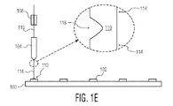
図1Eに図示するように、ワイヤ・ボンディング・ツール104およびワイヤクランプ108(例えば、閉位置であるが、所望する場合には開位置でもよい)は、ボールボンド112から連続して伸び、変形/切り欠きワイヤ部分118を有するワイヤ110とともにボールボンド112の上方の位置に上昇される。かかる位置は、従来のワイヤルーピングの専門用語でのループの頂点(すなわち、top of loop:TOL)位置と考えることができる。
As shown in FIG. 1E, the
図1Fでは、ワイヤクランプ108は開位置に移動し、ワイヤ・ボンディング・ツール104および開位置のワイヤクランプ108は矢印のように上向きのZ方向に上昇され、変形/切り欠きワイヤ部分118から連続して伸びるワイヤの別の部分114'(例えば、ワイヤ114'のテール長さ)がワイヤ・ボンディング・ツールの先端部120から繰り出される。例えば、ワイヤ部分114'は、次のイニシャルボールのワイヤテールになる。図1E〜図1Fのボンディングツール104の先端部120下方の円形拡大部分により明瞭に示すように、ワイヤ110の押圧されたワイヤ部分118はワイヤ110の部分的な切り欠きであってもよく、ワイヤ部分114と114'とを分離する。図1Gに図示するように、ワイヤクランプ108は、ワイヤ110の上部に接触して閉鎖されており、次いで、図1Hに図示するように、ワイヤ・ボンディング・ツール104およびワイヤクランプ108は、矢印のように上向きのZ方向に上昇され、それにより、ワイヤ110が変形/切り欠きワイヤ部分118の近傍で分離されてワイヤ配線構造122が形成される。ボンディングツール104の先端部下方の円形拡大部分により明瞭に示すように、(ワイヤ部分114'から分離した)ワイヤ配線構造122は、上方に向かって先細りになった端部、または尖った端部124を有してもよい。図1Iは、上記の方法の繰り返しによって追加的なボンディング位置102上に形成された他のワイヤ配線構造122を有する基板100を図示する。図示するように、ワイヤ配線構造122は、垂直に立っていても、または実質的にそのようになっていてもよい。
In FIG. 1F, the
図1Dと関連して、上記されるように、ワイヤ114の一部分は、別の位置116に対して押圧される。図1A〜図1Hの実施形態では、別の位置116は、基板100の一部分(例えば、基板100の表面部分、等々)であってもよい。しかしながら、別の位置116として任意の位置を使用してもよいことが当業者によって理解される。例えば、図2に図示するように、本発明の別の実施形態によれば、ワイヤ部分118(基板100上に形成されるワイヤ配線構造122の一部または全部)の押圧は、図2に示すように、基板100の(直接的な)一部ではない別の位置/基板200におけるなどの、基板100以外(例えば、別の基板または構造上)の位置で行われてもよい。
As described above in connection with FIG. 1D, a portion of
本発明によって形成されるワイヤ配線構造では、高さおよび結果として生じるワイヤテイル長さの一貫性が改善され、ならびに生産の効率が上昇する(例えば、1時間あたりの生産ユニット数)。 The wire wiring structure formed according to the present invention improves the consistency of the height and the resulting wire tail length, and increases production efficiency (eg, number of production units per hour).
本発明によって形成されるワイヤ配線構造は、中でも例えば、プローブカードの接点構造として、積層されたダイの用途でのダイの間の配線として、フリップチップ用途での配線として、Si貫通電極(through silicon via)用途、またはモールド貫通配線(through mold via)用途での配線として、パッケージオンパッケージ(package on package:POP)用途でのパッケージ間の配線として、使用されてもよい。 The wire wiring structure formed by the present invention is, for example, as a contact structure of a probe card, as a wiring between dies in the use of stacked dies, as a wiring in a flip chip application, as a through silicon via (through silicon) Vias, or as wiring for through mold vias, may be used as wiring between packages in package on package (POP) applications.
本発明について、主に、特定の例示的な方法の工程に関して所定の順序で記載してきたが、本発明はそのような方法の工程に限定されるものではない。前記工程の一部は、本発明の範囲内で再構成あるいは省略されてもよく、もしくは追加的な工程が追加されてもよい。 Although the present invention has been described primarily in a predetermined order with respect to certain exemplary method steps, the present invention is not limited to such method steps. Some of the steps may be reconfigured or omitted within the scope of the present invention, or additional steps may be added.
本発明は、特定の実施形態を参照して本明細書に図示され、かつ記載されているが、本発明は、示される詳細に限定されることを意図しない。むしろ、特許請求の範囲の均等物の範囲内で、かつ本発明から逸脱しない範囲内で、詳細では様々な変更がなされてもよい。 Although the invention is illustrated and described herein with reference to specific embodiments, the invention is not intended to be limited to the details shown. Rather, various changes may be made in detail within the scope of equivalents of the claims and without departing from the present invention.
Claims (21)
(a)ワイヤ・ボンディング・ツールを使用して基板上のボンディング位置にワイヤボンドを形成する工程と、
(b)前記ワイヤボンドから連続して伸びる所定の長さのワイヤを前記基板上において前記ボンディング位置とは別の位置まで延長させる工程と、
(c)前記ワイヤ・ボンディング・ツールを使用して前記連続して伸びる所定の長さのワイヤの一部分を前記基板上の前記別の位置に対して押圧する工程と、
(d)前記ワイヤ・ボンディング・ツールおよび前記連続して伸びる所定の長さのワイヤの前記押圧された一部分を前記ワイヤボンドの上方の位置へ移動する工程であって、前記押圧された一部分は、前記ワイヤボンドの延長上にあるものである、前記移動する工程と、
(e)前記連続して伸びる所定の長さのワイヤを前記押圧された一部分においてワイヤ供給から分離し、前記ボンディング位置に対してボンディングされたワイヤ配線構造を提供する工程と
を有する方法。 A method of forming a wire wiring structure,
(A) forming a wire bond at a bonding position on the substrate using a wire bonding tool;
(B) extending a wire having a predetermined length continuously extending from the wire bond to a position different from the bonding position on the substrate;
(C) pressing a portion of the continuously extending wire of predetermined length against the other location on the substrate using the wire bonding tool;
And (d) a step of moving the pressing has been first portion of the wire bonding tool and said continuously extending a predetermined length wire to a position above the wire bonds, said the pressed portion is The moving step being on an extension of the wire bond ; and
(E) a method and a step of the successive predetermined lengths of wire extending separated from the wire supply in the press has been first portion to provide a bonded wires wiring structure with respect to the bonding position.
工程(a)において、前記ワイヤボンドを形成するために使用されるイニシャルボールを形成する工程を有するものである方法。 The method of claim 1, further comprising:
A method comprising the step of forming an initial ball used for forming the wire bond in the step (a).
(d1)工程(d)と工程(e)との間に、前記連続して伸びる所定の長さのワイヤの前記押圧された一部分の上方に前記ボンディングツールから追加の長さのワイヤを延長させる工程を有するものである方法。 The method of claim 1, further comprising:
(D1) between steps (d) and the step (e), extending the additional length of wire from the bonding tool above the the pressed first portion of the predetermined length of the wire extending the succession The method which has a process to make.
工程(dl)の後で、且つ工程(e)の前に、ワイヤの上方部分に対してワイヤクランプを閉鎖させる工程を有するものである方法。 The method of claim 7, further comprising:
A method comprising the step of closing the wire clamp against the upper part of the wire after step (dl) and before step (e).
前記ワイヤ配線構造を使用して前記基板を別の隣接する基板に電気的に接続する工程を有するものである方法。 The method of claim 1, further comprising:
Using the wire wiring structure to electrically connect the substrate to another adjacent substrate.
工程(d)の後で、且つ工程(e)の前に、ワイヤの上方部分に対してワイヤクランプを閉鎖させる工程を有するものである方法。 The method of claim 1, further comprising:
A method comprising closing the wire clamp with respect to the upper portion of the wire after step (d) and before step (e).
(a)ワイヤ・ボンディング・ツールを使用して基板上のボンディング位置にボールボンドを形成する工程と、
(b)前記ボールボンドから連続して伸びる所定の長さのワイヤを前記基板上において前記ボンディング位置とは別の位置まで延長させる工程と、
(c)前記ワイヤ・ボンディング・ツールを使用して前記所定の長さのワイヤの一部分を前記基板上の前記別の位置に対して押圧して、当該ワイヤの一部分に部分的な切り欠き部分を形成する工程と、
(d)前記ワイヤ・ボンディング・ツールおよび前記所定の長さのワイヤの前記部分的な切り欠き部分を前記ボールボンドの上方の位置へ移動する工程であって、前記部分的な切り欠き部分は、前記ボールボンドの延長上にあるものである、前記移動する工程と、
(e)前記所定の長さのワイヤの前記部分的な切り欠き部分の上方に前記ワイヤ・ボンディング・ツールから追加の長さのワイヤを延長させる工程と、
(f)前記所定の長さのワイヤを前記部分的な切り欠き部分においてワイヤ供給から分離し、前記ボンディング位置に対してボンディングされたワイヤ配線構造を提供する工程であって、前記ワイヤ配線構造は前記ボールボンドの上方に垂直に延長するものである、前記分離する工程と
を有する方法。 A method of forming a wire wiring structure,
(A) forming a ball bond at a bonding position on the substrate using a wire bonding tool;
(B) extending a wire having a predetermined length continuously extending from the ball bond to a position different from the bonding position on the substrate;
(C) using the wire bonding tool to press a portion of the predetermined length of wire against the other position on the substrate to provide a partial notch in the portion of the wire; Forming, and
(D) moving the partial notch portion of the wire bonding tool and the predetermined length of wire to a position above the ball bond , wherein the partial notch portion comprises: The moving step being on an extension of the ball bond ;
(E) a step of extending the predetermined length of the wire the partial cut-out portion the wire bonding from tool additional length of wire over of,
(F) said predetermined length of wire is separated from the wire supply in the partial cut-out portion, providing a Bonn de Ingu by wire interconnect structure with respect to the bonding position, the wire wiring structure is for vertical directly extend above the ball bond, a method and a step of the separation.
工程(a)において、前記ボールボンドを形成するために使用されるイニシャルボールを形成する工程を有するものである方法。 15. The method of claim 14 , further comprising:
A method comprising a step of forming an initial ball used for forming the ball bond in the step (a).
工程(e)の後で、且つ工程(f)の前に、ワイヤの上方部分に対してワイヤクランプを閉鎖させる工程を有するものである方法。 15. The method of claim 14 , further comprising:
A method comprising closing the wire clamp with respect to the upper portion of the wire after step (e) and before step (f).
前記ワイヤ配線構造を使用して前記基板を別の隣接する基板に電気的に接続する工程を有するものである方法。 15. The method of claim 14 , further comprising:
Using the wire wiring structure to electrically connect the substrate to another adjacent substrate.
Applications Claiming Priority (3)
| Application Number | Priority Date | Filing Date | Title |
|---|---|---|---|
| US201261672449P | 2012-07-17 | 2012-07-17 | |
| US61/672,449 | 2012-07-17 | ||
| PCT/US2013/048860 WO2014014643A1 (en) | 2012-07-17 | 2013-07-01 | Methods of forming wire interconnect structures |
Publications (3)
| Publication Number | Publication Date |
|---|---|
| JP2015533258A JP2015533258A (en) | 2015-11-19 |
| JP2015533258A5 JP2015533258A5 (en) | 2016-06-16 |
| JP6297553B2 true JP6297553B2 (en) | 2018-03-20 |
Family
ID=49949169
Family Applications (1)
| Application Number | Title | Priority Date | Filing Date |
|---|---|---|---|
| JP2015523103A Active JP6297553B2 (en) | 2012-07-17 | 2013-07-01 | Method for forming a wire wiring structure |
Country Status (6)
| Country | Link |
|---|---|
| US (3) | US9502371B2 (en) |
| JP (1) | JP6297553B2 (en) |
| KR (1) | KR102094563B1 (en) |
| CN (1) | CN104471693B (en) |
| TW (1) | TWI531015B (en) |
| WO (1) | WO2014014643A1 (en) |
Cited By (3)
| Publication number | Priority date | Publication date | Assignee | Title |
|---|---|---|---|---|
| KR20230074797A (en) | 2021-09-16 | 2023-05-31 | 가부시키가이샤 신가와 | Pin wire forming method, and wire bonding device |
| KR20230088502A (en) | 2020-11-25 | 2023-06-19 | 가부시키가이샤 신가와 | Semiconductor device manufacturing method and semiconductor device manufacturing device |
| US11887963B2 (en) | 2020-08-17 | 2024-01-30 | Kioxia Corporation | Semiconductor device |
Families Citing this family (8)
| Publication number | Priority date | Publication date | Assignee | Title |
|---|---|---|---|---|
| WO2014014643A1 (en) * | 2012-07-17 | 2014-01-23 | Kulicke And Soffa Industries, Inc. | Methods of forming wire interconnect structures |
| US9870946B2 (en) * | 2013-12-31 | 2018-01-16 | Taiwan Semiconductor Manufacturing Company, Ltd. | Wafer level package structure and method of forming same |
| JP5686912B1 (en) * | 2014-02-20 | 2015-03-18 | 株式会社新川 | Bump forming method, bump forming apparatus, and semiconductor device manufacturing method |
| US10256208B2 (en) | 2014-10-03 | 2019-04-09 | Intel Corporation | Overlapping stacked die package with vertical columns |
| US11145620B2 (en) * | 2019-03-05 | 2021-10-12 | Asm Technology Singapore Pte Ltd | Formation of bonding wire vertical interconnects |
| US11543362B2 (en) * | 2019-05-02 | 2023-01-03 | Asmpt Singapore Pte. Ltd. | Method for measuring the heights of wire interconnections |
| KR20220045684A (en) | 2020-10-06 | 2022-04-13 | 에스케이하이닉스 주식회사 | Semiconductor Package Including a Wire Having a Zigzag Shape |
| US20220199570A1 (en) * | 2020-12-18 | 2022-06-23 | Kulicke And Soffa Industries, Inc. | Methods of forming wire interconnect structures and related wire bonding tools |
Family Cites Families (27)
| Publication number | Priority date | Publication date | Assignee | Title |
|---|---|---|---|---|
| US4213556A (en) * | 1978-10-02 | 1980-07-22 | General Motors Corporation | Method and apparatus to detect automatic wire bonder failure |
| DE3536908A1 (en) * | 1984-10-18 | 1986-04-24 | Sanyo Electric Co., Ltd., Moriguchi, Osaka | INDUCTIVE ELEMENT AND METHOD FOR PRODUCING THE SAME |
| US5045975A (en) * | 1987-05-21 | 1991-09-03 | Cray Computer Corporation | Three dimensionally interconnected module assembly |
| US5195237A (en) * | 1987-05-21 | 1993-03-23 | Cray Computer Corporation | Flying leads for integrated circuits |
| US5172851A (en) * | 1990-09-20 | 1992-12-22 | Matsushita Electronics Corporation | Method of forming a bump electrode and manufacturing a resin-encapsulated semiconductor device |
| US6295729B1 (en) * | 1992-10-19 | 2001-10-02 | International Business Machines Corporation | Angled flying lead wire bonding process |
| US6835898B2 (en) * | 1993-11-16 | 2004-12-28 | Formfactor, Inc. | Electrical contact structures formed by configuring a flexible wire to have a springable shape and overcoating the wire with at least one layer of a resilient conductive material, methods of mounting the contact structures to electronic components, and applications for employing the contact structures |
| US6836962B2 (en) * | 1993-11-16 | 2005-01-04 | Formfactor, Inc. | Method and apparatus for shaping spring elements |
| US5421503A (en) * | 1994-08-24 | 1995-06-06 | Kulicke And Soffa Investments, Inc. | Fine pitch capillary bonding tool |
| JPH09289276A (en) | 1996-04-23 | 1997-11-04 | Hitachi Ltd | Lead frame and semiconductor device using it |
| DE69739125D1 (en) * | 1996-10-01 | 2009-01-02 | Panasonic Corp | Capillary for wire bonding for the production of bump electrodes |
| JPH10135219A (en) * | 1996-10-29 | 1998-05-22 | Taiyo Yuden Co Ltd | Bump-forming method |
| JPH10135220A (en) | 1996-10-29 | 1998-05-22 | Taiyo Yuden Co Ltd | Bump-forming method |
| JP3189115B2 (en) * | 1996-12-27 | 2001-07-16 | 株式会社新川 | Semiconductor device and wire bonding method |
| US7032311B2 (en) * | 2002-06-25 | 2006-04-25 | Eli Razon | Stabilized wire bonded electrical connections and method of making same |
| US7229906B2 (en) * | 2002-09-19 | 2007-06-12 | Kulicke And Soffa Industries, Inc. | Method and apparatus for forming bumps for semiconductor interconnections using a wire bonding machine |
| JP3854232B2 (en) * | 2003-02-17 | 2006-12-06 | 株式会社新川 | Bump forming method and wire bonding method |
| US6815836B2 (en) * | 2003-03-24 | 2004-11-09 | Texas Instruments Incorporated | Wire bonding for thin semiconductor package |
| US7227095B2 (en) * | 2003-08-06 | 2007-06-05 | Micron Technology, Inc. | Wire bonders and methods of wire-bonding |
| WO2006013751A1 (en) * | 2004-08-05 | 2006-02-09 | Seiko Epson Corporation | Bonding structure, wire bonding method, actuator device and liquid injecting head |
| JP4298665B2 (en) * | 2005-02-08 | 2009-07-22 | 株式会社新川 | Wire bonding method |
| US7255538B2 (en) * | 2005-02-09 | 2007-08-14 | Hamilton Sundstrand Corporation | Shrink-fit stress coupling for a shaft of differing materials |
| JP4744238B2 (en) * | 2005-08-29 | 2011-08-10 | 田中電子工業株式会社 | Wire cutting method |
| JP4530975B2 (en) | 2005-11-14 | 2010-08-25 | 株式会社新川 | Wire bonding method |
| JP4509043B2 (en) * | 2006-02-14 | 2010-07-21 | 株式会社新川 | Stud bump formation method |
| JPWO2008117488A1 (en) * | 2007-03-23 | 2010-07-08 | 三洋電機株式会社 | Semiconductor device and manufacturing method thereof |
| WO2014014643A1 (en) * | 2012-07-17 | 2014-01-23 | Kulicke And Soffa Industries, Inc. | Methods of forming wire interconnect structures |
-
2013
- 2013-07-01 WO PCT/US2013/048860 patent/WO2014014643A1/en active Application Filing
- 2013-07-01 US US14/413,475 patent/US9502371B2/en active Active
- 2013-07-01 CN CN201380037938.4A patent/CN104471693B/en active Active
- 2013-07-01 KR KR1020157000968A patent/KR102094563B1/en active IP Right Grant
- 2013-07-01 JP JP2015523103A patent/JP6297553B2/en active Active
- 2013-07-12 TW TW102125018A patent/TWI531015B/en active
-
2016
- 2016-10-20 US US15/298,406 patent/US9865560B2/en active Active
-
2017
- 2017-08-16 US US15/678,619 patent/US10153247B2/en active Active
Cited By (3)
| Publication number | Priority date | Publication date | Assignee | Title |
|---|---|---|---|---|
| US11887963B2 (en) | 2020-08-17 | 2024-01-30 | Kioxia Corporation | Semiconductor device |
| KR20230088502A (en) | 2020-11-25 | 2023-06-19 | 가부시키가이샤 신가와 | Semiconductor device manufacturing method and semiconductor device manufacturing device |
| KR20230074797A (en) | 2021-09-16 | 2023-05-31 | 가부시키가이샤 신가와 | Pin wire forming method, and wire bonding device |
Also Published As
| Publication number | Publication date |
|---|---|
| US20170345787A1 (en) | 2017-11-30 |
| KR20150036074A (en) | 2015-04-07 |
| TWI531015B (en) | 2016-04-21 |
| TW201405683A (en) | 2014-02-01 |
| US9865560B2 (en) | 2018-01-09 |
| CN104471693B (en) | 2018-05-08 |
| US20170040280A1 (en) | 2017-02-09 |
| CN104471693A (en) | 2015-03-25 |
| KR102094563B1 (en) | 2020-03-27 |
| JP2015533258A (en) | 2015-11-19 |
| US20150132888A1 (en) | 2015-05-14 |
| US10153247B2 (en) | 2018-12-11 |
| US9502371B2 (en) | 2016-11-22 |
| WO2014014643A1 (en) | 2014-01-23 |
Similar Documents
| Publication | Publication Date | Title |
|---|---|---|
| JP6297553B2 (en) | Method for forming a wire wiring structure | |
| JP5714195B2 (en) | Manufacturing method of semiconductor device | |
| JP2007535820A (en) | Low loop wire bonding systems and methods | |
| TWI762533B (en) | Manufacturing method of semiconductor device | |
| KR101641102B1 (en) | Conductive bumps, wire loops, and methods of forming the same | |
| US10643966B2 (en) | Electrical interconnections for semiconductor devices and methods for forming the same | |
| JP4666592B2 (en) | Manufacturing method of semiconductor device | |
| JP2005159267A (en) | Semiconductor and wire bonding method | |
| US20180261567A1 (en) | Window Clamp | |
| CN104916609B (en) | Semiconductor device and wedge bond device | |
| JP3813135B2 (en) | Wire bonding method | |
| KR100660821B1 (en) | Wire bonding method | |
| JP2010073747A (en) | Wire bonding method and semiconductor device | |
| KR20080103072A (en) | Aluminum bump bonding for fine aluminum wire | |
| CN114725009A (en) | Method of forming lead interconnect structure and related wire bonding tool | |
| Camenforte et al. | Enabling Cu wire in 3D stack package | |
| JP2009076767A (en) | Method of manufacturing semiconductor apparatus, and wire bonding apparatus | |
| Camenforte et al. | Enabling Cu wire in 3D stack package QFN | |
| JP2008192713A (en) | Chip-laminated semiconductor device and its manufacturing method |
Legal Events
| Date | Code | Title | Description |
|---|---|---|---|
| A521 | Request for written amendment filed |
Free format text: JAPANESE INTERMEDIATE CODE: A523 Effective date: 20160421 |
|
| A621 | Written request for application examination |
Free format text: JAPANESE INTERMEDIATE CODE: A621 Effective date: 20160421 |
|
| A977 | Report on retrieval |
Free format text: JAPANESE INTERMEDIATE CODE: A971007 Effective date: 20170207 |
|
| A131 | Notification of reasons for refusal |
Free format text: JAPANESE INTERMEDIATE CODE: A131 Effective date: 20170214 |
|
| A601 | Written request for extension of time |
Free format text: JAPANESE INTERMEDIATE CODE: A601 Effective date: 20170512 |
|
| A601 | Written request for extension of time |
Free format text: JAPANESE INTERMEDIATE CODE: A601 Effective date: 20170714 |
|
| A521 | Request for written amendment filed |
Free format text: JAPANESE INTERMEDIATE CODE: A523 Effective date: 20170812 |
|
| TRDD | Decision of grant or rejection written | ||
| A01 | Written decision to grant a patent or to grant a registration (utility model) |
Free format text: JAPANESE INTERMEDIATE CODE: A01 Effective date: 20180206 |
|
| A61 | First payment of annual fees (during grant procedure) |
Free format text: JAPANESE INTERMEDIATE CODE: A61 Effective date: 20180221 |
|
| R150 | Certificate of patent or registration of utility model |
Ref document number: 6297553 Country of ref document: JP Free format text: JAPANESE INTERMEDIATE CODE: R150 |
|
| R250 | Receipt of annual fees |
Free format text: JAPANESE INTERMEDIATE CODE: R250 |
|
| R250 | Receipt of annual fees |
Free format text: JAPANESE INTERMEDIATE CODE: R250 |
|
| R250 | Receipt of annual fees |
Free format text: JAPANESE INTERMEDIATE CODE: R250 |
|
| R250 | Receipt of annual fees |
Free format text: JAPANESE INTERMEDIATE CODE: R250 |