JP6273194B2 - Electrostatic membrane diffusion bonding structure and process - Google Patents
Electrostatic membrane diffusion bonding structure and process Download PDFInfo
- Publication number
- JP6273194B2 JP6273194B2 JP2014242764A JP2014242764A JP6273194B2 JP 6273194 B2 JP6273194 B2 JP 6273194B2 JP 2014242764 A JP2014242764 A JP 2014242764A JP 2014242764 A JP2014242764 A JP 2014242764A JP 6273194 B2 JP6273194 B2 JP 6273194B2
- Authority
- JP
- Japan
- Prior art keywords
- conductive layer
- layer
- patterned
- dielectric layer
- actuator
- Prior art date
- Legal status (The legal status is an assumption and is not a legal conclusion. Google has not performed a legal analysis and makes no representation as to the accuracy of the status listed.)
- Active
Links
- 238000009792 diffusion process Methods 0.000 title claims description 9
- 238000000034 method Methods 0.000 title description 45
- 239000012528 membrane Substances 0.000 title description 28
- 239000000758 substrate Substances 0.000 claims description 22
- 239000004065 semiconductor Substances 0.000 claims description 17
- 239000010410 layer Substances 0.000 description 226
- 150000004767 nitrides Chemical class 0.000 description 34
- 239000000463 material Substances 0.000 description 13
- 238000005530 etching Methods 0.000 description 12
- 229910052751 metal Inorganic materials 0.000 description 11
- 239000002184 metal Substances 0.000 description 11
- XUIMIQQOPSSXEZ-UHFFFAOYSA-N Silicon Chemical compound [Si] XUIMIQQOPSSXEZ-UHFFFAOYSA-N 0.000 description 6
- 238000000151 deposition Methods 0.000 description 6
- 230000008021 deposition Effects 0.000 description 6
- 238000005137 deposition process Methods 0.000 description 6
- 229910052710 silicon Inorganic materials 0.000 description 6
- 239000010703 silicon Substances 0.000 description 6
- 239000003989 dielectric material Substances 0.000 description 4
- 238000012545 processing Methods 0.000 description 4
- 229910052581 Si3N4 Inorganic materials 0.000 description 3
- BQCADISMDOOEFD-UHFFFAOYSA-N Silver Chemical compound [Ag] BQCADISMDOOEFD-UHFFFAOYSA-N 0.000 description 3
- 239000000853 adhesive Substances 0.000 description 3
- 230000001070 adhesive effect Effects 0.000 description 3
- 229910052782 aluminium Inorganic materials 0.000 description 3
- XAGFODPZIPBFFR-UHFFFAOYSA-N aluminium Chemical compound [Al] XAGFODPZIPBFFR-UHFFFAOYSA-N 0.000 description 3
- 238000011065 in-situ storage Methods 0.000 description 3
- 238000002955 isolation Methods 0.000 description 3
- 239000000203 mixture Substances 0.000 description 3
- HQVNEWCFYHHQES-UHFFFAOYSA-N silicon nitride Chemical compound N12[Si]34N5[Si]62N3[Si]51N64 HQVNEWCFYHHQES-UHFFFAOYSA-N 0.000 description 3
- 229910052709 silver Inorganic materials 0.000 description 3
- 239000004332 silver Substances 0.000 description 3
- 238000004544 sputter deposition Methods 0.000 description 3
- 238000005229 chemical vapour deposition Methods 0.000 description 2
- 239000011248 coating agent Substances 0.000 description 2
- 238000000576 coating method Methods 0.000 description 2
- 238000004891 communication Methods 0.000 description 2
- 238000005516 engineering process Methods 0.000 description 2
- 230000008020 evaporation Effects 0.000 description 2
- 238000001704 evaporation Methods 0.000 description 2
- 238000000059 patterning Methods 0.000 description 2
- 229920002120 photoresistant polymer Polymers 0.000 description 2
- 238000005240 physical vapour deposition Methods 0.000 description 2
- 238000000623 plasma-assisted chemical vapour deposition Methods 0.000 description 2
- 229910001374 Invar Inorganic materials 0.000 description 1
- 229910001030 Iron–nickel alloy Inorganic materials 0.000 description 1
- 239000002253 acid Substances 0.000 description 1
- 239000012790 adhesive layer Substances 0.000 description 1
- 230000015572 biosynthetic process Effects 0.000 description 1
- 238000011109 contamination Methods 0.000 description 1
- 230000007423 decrease Effects 0.000 description 1
- 230000005684 electric field Effects 0.000 description 1
- 230000007613 environmental effect Effects 0.000 description 1
- 239000000945 filler Substances 0.000 description 1
- 238000007641 inkjet printing Methods 0.000 description 1
- 238000005259 measurement Methods 0.000 description 1
- 230000008018 melting Effects 0.000 description 1
- 238000002844 melting Methods 0.000 description 1
- 238000002156 mixing Methods 0.000 description 1
- 238000012986 modification Methods 0.000 description 1
- 230000004048 modification Effects 0.000 description 1
- 238000007639 printing Methods 0.000 description 1
- 239000011347 resin Substances 0.000 description 1
- 229920005989 resin Polymers 0.000 description 1
- 238000012360 testing method Methods 0.000 description 1
- TXEYQDLBPFQVAA-UHFFFAOYSA-N tetrafluoromethane Chemical compound FC(F)(F)F TXEYQDLBPFQVAA-UHFFFAOYSA-N 0.000 description 1
- 238000012546 transfer Methods 0.000 description 1
- 238000005019 vapor deposition process Methods 0.000 description 1
Images


Classifications
-
- B—PERFORMING OPERATIONS; TRANSPORTING
- B41—PRINTING; LINING MACHINES; TYPEWRITERS; STAMPS
- B41J—TYPEWRITERS; SELECTIVE PRINTING MECHANISMS, i.e. MECHANISMS PRINTING OTHERWISE THAN FROM A FORME; CORRECTION OF TYPOGRAPHICAL ERRORS
- B41J2/00—Typewriters or selective printing mechanisms characterised by the printing or marking process for which they are designed
- B41J2/005—Typewriters or selective printing mechanisms characterised by the printing or marking process for which they are designed characterised by bringing liquid or particles selectively into contact with a printing material
- B41J2/01—Ink jet
- B41J2/135—Nozzles
- B41J2/14—Structure thereof only for on-demand ink jet heads
- B41J2/14314—Structure of ink jet print heads with electrostatically actuated membrane
-
- B—PERFORMING OPERATIONS; TRANSPORTING
- B41—PRINTING; LINING MACHINES; TYPEWRITERS; STAMPS
- B41J—TYPEWRITERS; SELECTIVE PRINTING MECHANISMS, i.e. MECHANISMS PRINTING OTHERWISE THAN FROM A FORME; CORRECTION OF TYPOGRAPHICAL ERRORS
- B41J2/00—Typewriters or selective printing mechanisms characterised by the printing or marking process for which they are designed
- B41J2/005—Typewriters or selective printing mechanisms characterised by the printing or marking process for which they are designed characterised by bringing liquid or particles selectively into contact with a printing material
- B41J2/01—Ink jet
- B41J2/135—Nozzles
- B41J2/16—Production of nozzles
- B41J2/1621—Manufacturing processes
- B41J2/1623—Manufacturing processes bonding and adhesion
-
- B—PERFORMING OPERATIONS; TRANSPORTING
- B41—PRINTING; LINING MACHINES; TYPEWRITERS; STAMPS
- B41J—TYPEWRITERS; SELECTIVE PRINTING MECHANISMS, i.e. MECHANISMS PRINTING OTHERWISE THAN FROM A FORME; CORRECTION OF TYPOGRAPHICAL ERRORS
- B41J2/00—Typewriters or selective printing mechanisms characterised by the printing or marking process for which they are designed
- B41J2/005—Typewriters or selective printing mechanisms characterised by the printing or marking process for which they are designed characterised by bringing liquid or particles selectively into contact with a printing material
- B41J2/01—Ink jet
- B41J2/135—Nozzles
- B41J2/16—Production of nozzles
- B41J2/1621—Manufacturing processes
- B41J2/1626—Manufacturing processes etching
-
- B—PERFORMING OPERATIONS; TRANSPORTING
- B41—PRINTING; LINING MACHINES; TYPEWRITERS; STAMPS
- B41J—TYPEWRITERS; SELECTIVE PRINTING MECHANISMS, i.e. MECHANISMS PRINTING OTHERWISE THAN FROM A FORME; CORRECTION OF TYPOGRAPHICAL ERRORS
- B41J2/00—Typewriters or selective printing mechanisms characterised by the printing or marking process for which they are designed
- B41J2/005—Typewriters or selective printing mechanisms characterised by the printing or marking process for which they are designed characterised by bringing liquid or particles selectively into contact with a printing material
- B41J2/01—Ink jet
- B41J2/135—Nozzles
- B41J2/16—Production of nozzles
- B41J2/1621—Manufacturing processes
- B41J2/1631—Manufacturing processes photolithography
-
- B—PERFORMING OPERATIONS; TRANSPORTING
- B41—PRINTING; LINING MACHINES; TYPEWRITERS; STAMPS
- B41J—TYPEWRITERS; SELECTIVE PRINTING MECHANISMS, i.e. MECHANISMS PRINTING OTHERWISE THAN FROM A FORME; CORRECTION OF TYPOGRAPHICAL ERRORS
- B41J2/00—Typewriters or selective printing mechanisms characterised by the printing or marking process for which they are designed
- B41J2/005—Typewriters or selective printing mechanisms characterised by the printing or marking process for which they are designed characterised by bringing liquid or particles selectively into contact with a printing material
- B41J2/01—Ink jet
- B41J2/135—Nozzles
- B41J2/16—Production of nozzles
- B41J2/1621—Manufacturing processes
- B41J2/164—Manufacturing processes thin film formation
- B41J2/1642—Manufacturing processes thin film formation thin film formation by CVD [chemical vapor deposition]
-
- B—PERFORMING OPERATIONS; TRANSPORTING
- B41—PRINTING; LINING MACHINES; TYPEWRITERS; STAMPS
- B41J—TYPEWRITERS; SELECTIVE PRINTING MECHANISMS, i.e. MECHANISMS PRINTING OTHERWISE THAN FROM A FORME; CORRECTION OF TYPOGRAPHICAL ERRORS
- B41J2/00—Typewriters or selective printing mechanisms characterised by the printing or marking process for which they are designed
- B41J2/005—Typewriters or selective printing mechanisms characterised by the printing or marking process for which they are designed characterised by bringing liquid or particles selectively into contact with a printing material
- B41J2/01—Ink jet
- B41J2/135—Nozzles
- B41J2/16—Production of nozzles
- B41J2/1621—Manufacturing processes
- B41J2/164—Manufacturing processes thin film formation
- B41J2/1646—Manufacturing processes thin film formation thin film formation by sputtering
Description
本教示は、インクジェット印刷デバイスの分野に関し、より詳細には静電駆動式インクジェットプリントヘッドのための方法および構造、ならびに静電駆動式インクジェットプリントヘッドを含むプリンタに関する。 The present teachings relate to the field of inkjet printing devices, and more particularly to methods and structures for electrostatically driven inkjet printheads, and printers that include electrostatically driven inkjet printheads.
ドロップ・オン・デマンドのインクジェット技術は、印刷産業において広く使用されている。ドロップ・オン・デマンドの技術を用いるプリンタは、複数の静電アクチュエータ、圧電アクチュエータ、またはサーマルアクチュエータを用いて、アパーチャプレートの複数のノゾルからインクを吐出できる。静電吐出において、基材アセンブリ上に形成された各静電アクチュエータは、通常、可撓性の隔膜または膜、このアパーチャプレートと膜との間のインクチャンバ、およびこのアクチュエータ膜と基材アセンブリとの間のエアチャンバを含む。静電アクチュエータはさらに、基材アセンブリ上に形成されたアクチュエータ電極を含む。電圧が印加されてアクチュエータ電極を活性化するとき、膜は、電場によって電極の方に引っ張られ、緩和状態から屈曲状態に駆動され、これによりインクチャンバの体積を増大し、インクはインク供給部または貯蔵部からインクチャンバにインクを引き込む。電圧が取り除かれてアクチュエータ電極を不活性化するとき、膜は緩和し、インクチャンバ内の体積が減少して、インクがアパーチャプレートのノズルから吐出される。 Drop-on-demand ink jet technology is widely used in the printing industry. Printers using drop-on-demand technology can eject ink from multiple nozzles on the aperture plate using multiple electrostatic, piezoelectric, or thermal actuators. In electrostatic discharge, each electrostatic actuator formed on a substrate assembly typically includes a flexible diaphragm or membrane, an ink chamber between the aperture plate and the membrane, and the actuator membrane and the substrate assembly. Between the air chambers. The electrostatic actuator further includes an actuator electrode formed on the substrate assembly. When a voltage is applied to activate the actuator electrode, the membrane is pulled toward the electrode by an electric field and driven from a relaxed state to a bent state, thereby increasing the volume of the ink chamber, and the ink is supplied to the ink supply or Ink is drawn from the reservoir into the ink chamber. When the voltage is removed to deactivate the actuator electrode, the membrane relaxes, the volume in the ink chamber decreases, and ink is ejected from the nozzles of the aperture plate.
静電アクチュエータの重要な態様の1つは、アクチュエータ電極と膜との間の空間またはギャップの寸法である。ギャップは、アクチュエータ電極からの電圧が取り除かれる際にノズルから吐出されるインクの体積と、膜を十分に歪めるのにアクチュエータ電極に印加されなければならない電圧との両方に影響を与える。非常に狭いまたは非常に広いギャップは、それぞれインクの不十分なまたは過剰の量のいずれかを吐出する。さらに、ギャップ高さが増大にするにつれて、膜を十分に歪めるためにアクチュエータ電極に印加されなければならない電力も増大する。 One important aspect of an electrostatic actuator is the size of the space or gap between the actuator electrode and the membrane. The gap affects both the volume of ink ejected from the nozzle when the voltage from the actuator electrode is removed and the voltage that must be applied to the actuator electrode to sufficiently distort the membrane. A very narrow or very wide gap will eject either an inadequate or excessive amount of ink, respectively. Furthermore, as the gap height increases, the power that must be applied to the actuator electrode to sufficiently distort the membrane also increases.
静電アクチュエータはさらに、アクチュエータ電極を形成するために使用される伝導層の部分に形成された誘電ギャップスタンドオフ層を含む。膜は、ギャップスタンドオフの上方面に接着または接合され、膜を電極から距離をあけて配置し、こうしてギャップスタンドオフ層の厚さが、アクチュエータ電極と膜との間のギャップを部分的に決定する。ギャップ高さはまた、ギャップスタンドオフに膜を接合させるために使用される技術によっても影響を受ける。接着剤層、例えばEPON(商標)(Miller Stephenson Chemical Co.(Danbury,CT)から入手可能)またはTechFilm i2300(Resin Designs,LLC(Woburn,MA)から入手可能)を、アクチュエータ電極と膜との間に介在させてもよく、次いで熱および圧力の適用中に硬化され、アクチュエータ膜をギャップスタンドオフに接合させる。しかし、このプロセスは、遊離接着剤によるアクチュエータのエアチャンバの汚染を受け易い。さらに、加工処理の変動は、最終的な接着剤厚さの精度に影響する場合があり、ターゲット高さから外れたギャップ高さの変動の一因となる。他のプロセスは、制限された範囲の材料でのみ成功し得るので、材料の選択が制限される。 The electrostatic actuator further includes a dielectric gap standoff layer formed on the portion of the conductive layer used to form the actuator electrode. The membrane is glued or bonded to the upper surface of the gap standoff, placing the membrane at a distance from the electrode, and thus the thickness of the gap standoff layer partially determines the gap between the actuator electrode and the membrane. To do. The gap height is also affected by the technique used to join the membrane to the gap standoff. An adhesive layer, such as EPON ™ (available from Miller Stephenson Chemical Co. (Danbury, CT)) or TechFilm i2300 (available from Resin Designs, LLC (Woburn, Mass.)) Between the actuator electrode and the membrane. And then cured during application of heat and pressure to bond the actuator membrane to the gap standoff. However, this process is susceptible to contamination of the actuator air chamber by free adhesive. Furthermore, variations in processing may affect the accuracy of the final adhesive thickness and contribute to variations in gap height that deviates from the target height. Other processes can only be successful with a limited range of materials, limiting the choice of materials.
一部の他の形成方法に関連した問題を克服する静電駆動式インクジェットプリントヘッドを形成するための方法、および環境条件を変化させる際により安定な操作を有する形成プロセスが所望される。 A method for forming an electrostatically driven inkjet printhead that overcomes the problems associated with some other forming methods and a forming process that has a more stable operation when changing environmental conditions are desired.
以下に、本教示の1つ以上の実施形態の一部の態様について基本的な理解を提供するために簡単な要約を示す。この要約は、広範囲の概説ではなく、本教示の主要なおよび重要な要素を同定することを意図することもなく、開示の範囲を詳述することも意図しない。さらにその主要な目的は、単に1つ以上の概念を後に示される詳細な説明の導入部として簡単な形態で示すことである。 The following is a brief summary in order to provide a basic understanding of some aspects of one or more embodiments of the present teachings. This summary is not an extensive overview, and it is not intended to identify key and critical elements of the present teachings or to detail the scope of the disclosure. Furthermore, its primary purpose is merely to present one or more concepts in a simplified form as a prelude to the more detailed description that is presented later.
実施形態において、プリントヘッドは、複数の静電アクチュエータを含み、ここで各静電アクチュエータは、半導体基材アセンブリを覆い、第1の部分を含むパターニングされた第1の伝導性層、パターニングされた第1の伝導性層の第1の部分と物理的および電気的に接触した第1の部分を有するパターニングされた第2の伝導性層であって、パターニングされた第2の伝導性層の第1の部分は、アクチュエータ電極の少なくとも一部である第2の伝導性層、ならびに半導体基材アセンブリを覆い、側壁を有する第1の誘電体層を含む。各静電アクチュエータはさらに、第1の誘電体層を覆う第2の誘電体層を含み、この側壁が、第2の誘導体層の下において側方に埋め込まれ、凹部を与える第2の誘電体層、第2の誘電体層上の第2の伝導性層の第2の部分、ならびに第2の伝導性層の第2の部分に拡散接合したアクチュエータ膜を含む。 In an embodiment, the printhead includes a plurality of electrostatic actuators, wherein each electrostatic actuator covers a semiconductor substrate assembly and includes a first portion patterned first conductive layer, patterned. A patterned second conductive layer having a first portion that is in physical and electrical contact with a first portion of the first conductive layer, the second portion of the patterned second conductive layer. One portion includes a second conductive layer that is at least part of the actuator electrode, as well as a first dielectric layer that covers the semiconductor substrate assembly and has sidewalls. Each electrostatic actuator further includes a second dielectric layer overlying the first dielectric layer, the sidewalls of which are embedded laterally under the second dielectric layer to provide a recess. And an actuator film diffusion bonded to the second portion of the second conductive layer on the second dielectric layer and the second portion of the second conductive layer.
別の実施形態において、プリントヘッドのための静電アクチュエータを形成するための方法は、半導体基材アセンブリにわたってパターニングされた第1の伝導性層を形成する工程であって、このパターニングされた第1の伝導性層が第1の部分を含む工程、第1の伝導性層にわたってブランケット第1の誘電体層を形成する工程、ブランケット第1の伝導性層にわたってブランケット第2の誘電体層を形成する工程、ならびにブランケット第2の誘電体層およびブランケット第1の誘電体層をパターニングして、パターニングされた第1の伝導性層の第1の部分を露呈する工程を含んでいてもよい。この方法がさらに、第1の誘電体層を等方的にエッチングし、第2の誘電体層の下において第1の誘電体層の側壁を側方にエッチングし、凹部を提供する工程、指向性堆積プロセスを用いて自己パターニングされた第2の伝導性層を形成する工程であって、この第2の伝導性層が、第1の伝導性層の第1の部分と物理的および電気的に接触する第1の部分を有する工程、ならびに少なくともアクチュエータ電極の一部および第2の誘電体層と物理的に接触する第2の部分を形成する工程であって、ここで第2の伝導性層の第1の部分が、第2の伝導性層の第2の部分から電気的に隔離している工程、アクチュエータ膜を第2の伝導性層の第2の部分に拡散接合する工程を含んでいてもよい。 In another embodiment, a method for forming an electrostatic actuator for a printhead includes forming a patterned first conductive layer over a semiconductor substrate assembly, the patterned first The conductive layer includes a first portion, forming a blanket first dielectric layer over the first conductive layer, and forming a blanket second dielectric layer over the blanket first conductive layer. And patterning the blanket second dielectric layer and the blanket first dielectric layer to expose a first portion of the patterned first conductive layer. The method further includes isotropically etching the first dielectric layer, etching the sidewalls of the first dielectric layer laterally under the second dielectric layer, and providing a recess. Forming a self-patterned second conductive layer using a reactive deposition process, wherein the second conductive layer is physically and electrically coupled with a first portion of the first conductive layer. And forming a second portion in physical contact with at least a portion of the actuator electrode and the second dielectric layer, wherein the second conductivity is provided. The first portion of the layer is electrically isolated from the second portion of the second conductive layer, and includes diffusion bonding the actuator film to the second portion of the second conductive layer. You may go out.
別の実施形態において、プリンタは、プリントヘッドを含んでいてもよく、ここでこのプリントヘッドは複数の静電アクチュエータを含み、ここで各静電アクチュエータは、半導体基材アセンブリを覆い、第1の部分を含むパターニングされた第1の伝導性層、パターニングされた第1の伝導性層の第1の部分と物理的および電気的に接触した第1の部分を有するパターニングされた第2の伝導性層であって、ここでパターニングされた第2の伝導性層の第1の部分が、アクチュエータ電極の少なくとも一部である第2の伝導性層、ならびに半導体基材アセンブリを覆い、側壁を有する第1の誘電体層を含む。各静電アクチュエータはさらに、第1の誘電体層を覆う第2の誘電体層であって、ここでこの側壁が、第2の誘電体層の下において側方に埋め込まれ、凹部を提供する第2の誘電体層、第2の誘電体層上の第2の伝導性層の第2の部分、ならびに第2の伝導性層の第2の部分に拡散接合したアクチュエータ膜を含む。プリンタはさらに、プリントヘッドを包み込むハウジングを含む。 In another embodiment, the printer may include a print head, wherein the print head includes a plurality of electrostatic actuators, wherein each electrostatic actuator covers the semiconductor substrate assembly, and the first A patterned first conductive layer including a portion, a patterned second conductive having a first portion in physical and electrical contact with the first portion of the patterned first conductive layer A first portion of the second conductive layer patterned here, covering the second conductive layer that is at least part of the actuator electrode, as well as the semiconductor substrate assembly, and having a sidewall. 1 dielectric layer. Each electrostatic actuator is further a second dielectric layer overlying the first dielectric layer, where the sidewall is buried laterally under the second dielectric layer to provide a recess. The actuator includes a second dielectric layer, a second portion of the second conductive layer on the second dielectric layer, and an actuator film diffusion bonded to the second portion of the second conductive layer. The printer further includes a housing that encloses the printhead.
本明細書に組み込まれ、本明細書の一部を構成する添付の図面は、本教示の実施形態を詳細な説明と共に例示し、開示の原理を説明するように作用する。図面において:
図の詳細部の一部は簡略化されており、構造上の厳密な精度、詳細および尺度を維持することよりも本教示の理解を促進するために描かれていることに留意すべきである。 It should be noted that some of the details in the figures are simplified and are drawn to facilitate an understanding of the present teachings rather than maintaining strict structural accuracy, details and scale. .
ここで、本教示の例示的な実施形態を詳細に参照する。この例は、添付の図面に例示される。可能である限り、同じ、同様のまたは似た部分を言及するために同じ参照番号を図面全体にわたって使用する。 Reference will now be made in detail to exemplary embodiments of the present teachings. This example is illustrated in the accompanying drawings. Wherever possible, the same reference numbers will be used throughout the drawings to refer to the same, like or like parts.
本明細書で使用される場合、特に断らない限り、用語「プリンタ」は、何らかの目的のためにプリント出力機能を果たすいずれかの装置、例えばデジタルコピー機、製本機、ファクシミリ機、多機能機、静電複写機などを包含する。 As used herein, unless otherwise specified, the term “printer” refers to any device that performs a print output function for any purpose, such as a digital copier, bookbinding machine, facsimile machine, multi-function machine, Includes electrostatic copying machines.
本教示の実施形態は、アクチュエータ膜と誘電体ギャップスタンドオフ層との間に改善された物理的な連結を有する静電アクチュエータをもたらし得る。プロセスおよび構造は、自己パターニングされ(すなわちin situでパターニングされ)、ほとんどまたは全く後続加工処理を必要としない最終金属層堆積を含むことができる。最終金属層を用いて、膜は、拡散プロセスを用いてギャップスタンドオフ層に接合され、結果として精密なギャップ高さと、膜と電極との間の電気的隔離をもたらし得る。 Embodiments of the present teachings can result in an electrostatic actuator having an improved physical connection between the actuator film and the dielectric gap standoff layer. The processes and structures can include a final metal layer deposition that is self-patterned (ie, patterned in situ) and requires little or no subsequent processing. With the final metal layer, the membrane can be bonded to the gap standoff layer using a diffusion process, resulting in precise gap height and electrical isolation between the membrane and the electrode.
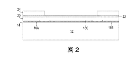
本教示の実施形態の間に形成できるインプロセス構造を図1〜6に示す。図に示された構造は、単純化のために示されていない追加の特徴を含んでいてもよいが、示された構造は取り除かれてもよく、または変更されてもよいことが理解される。図1のインプロセス静電アクチュエータ構造10は、半導体基材アセンブリ12、ブランケット誘電体層14、第1の伝導性層16(例えば、金属1層)、およびパターニングされた第1のマスク層18を含む。本明細書の種々の実施形態において、半導体基材アセンブリ12は、シリコンウェハまたはウェハセクションを含んでいてもよく、種々の他の層(単純化のために示されていない)、例えば種々のドープされた領域および1つ以上の層、例えば酸化物層(この層の上にブランケット誘電体層14が形成される)をさらに含んでいてもよい。ブランケット誘電体層14は、約0.01μm〜約1.0μm厚さの窒化ケイ素または酸窒化ケイ素のような窒化物層を含んでいてもよい。伝導性層16は、約0.1μm〜約0.6μm厚さのアルミニウム層を含んでいてもよい。フォトレジストまたは別のマスクであってもよいパターニングされたマスク層18は、伝導性層16の第1の部分を露呈し、伝導性層16の第2の部分を覆う。続いて、エッチングが行われて、伝導性層16の露呈した第1の部分を除去し、誘電体層14上で停止させ、これにより図2に示されるように、パターニングされた伝導性層16を形成する。好適なエッチングは当該技術分野において既知である。伝導性層16をエッチングした後、マスク層18が除去され、これにより結果として伝導性部分16A、16Bおよび16Cを得る。実施形態において、伝導性層16の部分16Cは、アクチュエータ電極を与え、部分16A、16Bは、以下に記載されるように、誘電体ギャップスタンドオフ層を支持する。
In-process structures that can be formed during embodiments of the present teachings are shown in FIGS. While the structure shown in the figures may include additional features not shown for simplicity, it is understood that the structure shown may be removed or changed. . The in-process
続いて、ブランケット酸化物層20を堆積させ、ブランケット窒化物層22を堆積させ、パターニングされた第2のマスク24を形成して、結果として図2に示される構造と同様の構造を得る。ブランケット酸化物20は、約0.1μm〜約2.0μmの厚さまで堆積されてもよく、ブランケット窒化物層22は、約0.01μm〜約1.0μmの厚さであってもよい。パターニングされた第2のマスク24は、ブランケット酸化物層20の第1の部分およびブランケット窒化物層22を露呈する。他の誘電体材料が好適であってもよいことが理解され、ここで誘電体層14、20、および22は、誘電体20が誘電体14および22に対して選択的にエッチングされ得るように選択される(すなわち、層20は、層14および22よりも迅速な速度でエッチングされ得る)。パターニングされた第2のマスク24は、アクチュエータエアチャンバの広さを規定し、伝導性層16の部分16Cを露呈するように配置され、これはアクチュエータ電極の部分を形成する。
Subsequently, a
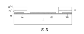
次に、図3に示されるように、ブランケット窒化物層22およびブランケット酸化物層20は、例えばほぼ垂直の異方性エッチングを用いてエッチングし、示されるように伝導性層16および窒化物層14を露呈する。実施形態において、第1のエッチング化学物質を使用して、窒化物層22の露呈部分を除去し、ブランケット酸化物層20上で停止させてもよく、次いで第2のエッチング化学物質を使用して、ブランケット酸化物層20の露呈部分を除去し、伝導性層16および窒化物層14上で停止させてもよい。
Next, as shown in FIG. 3,
続いて、第2のマスク層24が除去され、酸化物層20の等方性エッチングが行われ、結果として図4の構造を得る。露呈した窒化物層14、22および伝導性層16を除去するよりも迅速な速度で酸化物層20の露呈部分を除去するエッチング化学物質を使用する。実施形態において、エッチング化学物質は、緩衝酸化物(すなわちBOE)エッチング、希フッ化水素(HF)酸、HFガス、およびテトラフルオロメタン(CF4)ガスブレンドを含んでいてもよい。酸化物層20の等方エッチングにより、窒化物層22のアンダーカットを行い、窒化物層22の下において、窒化物層14、22の間にある酸化物層20の側壁40を側方に(すなわち図4に示されるように水平に)埋め込む。実施形態において、酸化物層20の側壁40は、窒化物層22の下において最も離れた位置で約0.1μm〜約1.0μm埋め込まれてもよい。図5に示される酸化物層20のそれぞれの側壁は、半円プロファイルを有するが、側壁は、垂直、ほぼ垂直であってもよく、または使用されるエッチングプロセスに依存して想定される他のプロファイルを有していてもよい。加えて、図5は第1のおよび第2の側壁40を示すが、側壁40は、部分的に、部分16Cを露呈する層16の部分16Cの周りに連続的な四角形または長方形の開口部、リング、またはポケットを規定することにより、示された断面において2つの別個の側壁として現れてもよいことが理解される。
Subsequently, the
次に、第2の伝導性層50(例えば、金属2層)が、図5に示されるように形成される。第2の伝導性層50は、例えば、非水平面、特に垂直もしくはほぼ垂直な面にわたるステップ被覆が劣る指向性堆積プロセス、例えばスパッタリングプロセス、エバポレーションプロセス、例えばサーマルまたはeビームエバポレーション、蒸着プロセス、例えば化学蒸着(CVD)、物理蒸着(PVD)、プラズマ強化CVD(PECVD)などを用いて形成されてもよい。ステップ被覆が劣る堆積の使用を用いるこれらのプロセスのそれぞれについて堆積パラメータは、本明細書の情報から当業者によって決定されてもよい。実施形態において、金属、例えば銀のスパッタリングプロセスは、第2の伝導性層50を形成するために使用されてもよい。酸化物層20の側壁40は、窒化物層14、22との間において側方に埋め込まれるので、第2の伝導性層50の指向性堆積は、結果として層50の部分50A、50Bが部分50Cから電気的に隔離するように材料ボイドをもたらす。故にこのプロセスは、自己パターニングされた(すなわちin situパターニングされた)層50を形成する。この開示の目的のために、自己パターニングされた層は、互いに電気的に隔離した2つ以上の部分を提供するために伝導性層の別個のマスクまたはエッチングを必要としないブランケット堆積プロセスを用いて形成された電気伝導性層である。この実施形態において、層50は、ブランケット堆積プロセスを用いて形成され、ここで部分50Cは、互いに電気的に隔離した部分を与えるために層50の別個のマスクされたエッチングを必要とせずに、部分50Aおよび50Bから電気的に隔離される。このプロセスにおいて、部分50A、50Bの部分50Cからの電気的隔離は、層50が酸化物層20のターゲット厚さよりも小さいターゲット厚さを有するように形成されさえすれば、得られる。一般に、酸化物層20は、伝導性層50より相当厚いターゲット厚さ、例えばそのターゲット厚さの約15〜約25倍を有する。実施形態において、層50は、約0.05μmのターゲット厚さを有していてもよいが、酸化物層20は約1.0μmのターゲット厚さを有する。部分50Aおよび50Bが部分50Cの周りにリングを形成し得るので、電気的に共にカップリングされてもよく、単一の連続構造を形成してもよいことが理解される。
Next, a second conductive layer 50 (eg, two metal layers) is formed as shown in FIG. The second conductive layer 50 is, for example, a directional deposition process with poor step coverage over a non-horizontal plane, particularly a vertical or nearly vertical plane, such as a sputtering process, an evaporation process, such as a thermal or e-beam evaporation, a vapor deposition process, For example, it may be formed using chemical vapor deposition (CVD), physical vapor deposition (PVD), plasma enhanced CVD (PECVD), or the like. The deposition parameters for each of these processes using the use of deposition with inferior step coverage may be determined by those skilled in the art from the information herein. In an embodiment, a metal, eg, silver, sputtering process may be used to form the second conductive layer 50. Since the
伝導性層50の部分50Cは、示されるように伝導性層16の部分16Cと物理的および電気的に接触する。故に伝導性層16の部分16Cおよび伝導性層50の部分50Cは、完成型アクチュエータ電極52を形成する。図5に示されるように、伝導性層50の部分50Cは、層16の部分16Cに直接形成され、これらと電気連通する。さらに、部分50Cは、部分16Cより広いので、完成型アクチュエータ電極52の幅を有効に増大させる。図5の断面に示されるように、アクチュエータ電極52は、窒化物層14のすべての露呈部分を被覆するので、アクチュエータ電極52の幅を最大化する。故にアクチュエータ52の部分50Cの幅は、自己パターニングされる。故にアクチュエータ電極52の主要な(すなわち外側の)幅は、アクチュエータ電極52の一部を形成する自己パターニングされた層50Cによって提供される。故にアクチュエータ電極52の外側縁部は、電気短絡のリスクなしでアクチュエータエアチャンバに整列される。部分50Cによって提供されるアクチュエータ電極52の外側縁部は、エッチングされた酸化物側壁40によって提供される凹部内において窒化物層22の下に直接形成されてもよい。
次に、層50の部分50Aおよび50Bを使用して、図6に示されるようにアクチュエータ膜60を物理的に取り付ける。実施形態において、膜60は、鉄ニッケル合金、例えばInvar(64FeNi)、ケイ素層、または別の好適な材料であってもよく、約2.0μm〜約40μmの厚さまたは約10μm〜約20μmの厚さを有する。膜60は、層50のために使用される同じまたは同様の金属の薄いコーティングを有していてもよい。実施形態において、膜60は、層50の部分50A、50Bと物理的に接触した状態にて圧力下(例えばプレスにて)で配置されてもよく、次いで加熱されて原子的に層50A、50Bを膜60と混ぜ合わせる。例えば、図6の構造は、約50psi〜約25,000psi、または約75psi〜約1,000psi、または約100psi〜約500psiの圧力下で、プレス内に配置されてもよく、約150℃〜約350℃の温度に加熱される。次いで構造は、冷却されて、伝導性層50A、50Bを用いて種々の介在層を通して膜60を半導体基材アセンブリ12に接合させてもよい。この拡散接合プロセスは、充填剤金属または他の別個の接着剤を必要とせずに、熱および圧力を用いることだけで層50A、50Bを膜60と接合する。接合温度は、層50と膜60との両方の融点未満である。理論に束縛されないが、層50および膜60の界面の原子は、界面にわたって移動し、グレイン境界がシフトし、マイクロギャップが低下される。層50の部分50A、50Bと膜60との間の最終境界は、この混ぜ合わせによって曖昧になる。アクチュエータ膜60の取り付けは、各アクチュエータ64のためにアクチュエータエアチャンバ62の形成を完了し、これは複数のアクチュエータを含むアクチュエータアレイの一部である。
Next,
層50の追加は、アクチュエータ電極52とアクチュエータ膜60との間のギャップ高さに影響を与えないことを理解されたい。例えば、部分50A、50Bは、部分50Cと同じ厚さを有し、故に部分50Cを含むアクチュエータ電極52と、アクチュエータ膜60の底部との間の正味の距離は、大抵の使用において埋め合わせを必要とする量までは変化しない。いずれかの埋め合わせが必要とされる場合、図6の1つ以上の層のターゲット堆積厚さは、調整されてもよい。
It should be understood that the addition of layer 50 does not affect the gap height between
図7〜13に示される別の実施形態において、2つの伝導性層を含むプロセスが、トレース経路密度を増大させるために使用されてもよい。第1の伝導性層、例えば金属1として使用されるアルミニウム層は、複数のトレースを形成するために使用されてもよく、第2の伝導性層、例えば金属2として使用される銀層は、アクチュエータ電極および拡散接合材料を形成するために使用されてもよい。図に示される構造は、単純化するために記載されていない追加の特徴を含んでいてもよいが、示された構造は除去または変更されてもよいことが理解される。 In another embodiment shown in FIGS. 7-13, a process including two conductive layers may be used to increase the trace path density. A first conductive layer, such as an aluminum layer used as metal 1, may be used to form a plurality of traces, and a second conductive layer, such as a silver layer used as metal 2, is It may be used to form actuator electrodes and diffusion bonding materials. While the structure shown in the figures may include additional features not described for simplicity, it will be understood that the structure shown may be removed or changed.
図7のインプロセス静電アクチュエータ構造70は、半導体基材アセンブリ12、ブランケット誘電体層14、第1の伝導性層16(例えば金属1層)、およびパターニングされた第1のマスク層72を含む。実施形態において、半導体基材アセンブリ12は、シリコンウェハまたはウェハセクションを含んでいてもよい。ブランケット誘電体層14は、窒化物層、例えば窒化ケイ素または酸窒化ケイ素、酸化物または別の誘導体を、例えば約0.01μm〜約1.0μm厚さで含んでいてもよい。伝導性層16は、約0.1μm〜約1.0μm厚さのアルミニウム層を含んでいてもよい。フォトレジストまたは別のマスクであってもよいパターニングされたマスク層72は、伝導性層16の第1の部分を露呈し、伝導性層16の第2の部分を覆う。続いて、エッチングは、伝導性層16の露呈した第1の部分を除去するためおよび誘電体層14にて停止するように行われ、これにより図8に示されるように層16から複数のトレース80を形成する。図において、層80の第1の部分「80A」は、示される静電アクチュエータのためのトレースを指定するが、層80の第2の部分「80B」は、プリントヘッド内の他の位置において示されていない静電アクチュエータに対して経路付けられるトレースを指定する。誘電体層14に対して選択的に伝導性層16をエッチングするために好適なエッチングは、当該技術分野において既知である。伝導性層16をエッチングした後、マスク層72を除去する。
The in-process
次に、平面のブランケット第2の誘電体層82および第2のマスク84が、図8に示されるように形成される。第2の誘電体層82は、窒化物、例えば窒化ケイ素または酸窒化ケイ素であってもよい。マスク層84は、トレース80の第1の部分(例えば示された位置におけるトレース「80A」および示されていない他のアクチュエータ電極位置におけるトレース80B)を露呈し、トレース80(例えば示されていない他の位置でのトレース「80A」)の第2の部分を被覆してもよい。一般に、各トレース80は、1つのアクチュエータ電極位置だけが第2のマスク層84によって露呈され、こうして各フィーチャアクチュエータ電極は、トレース80の1つを用いて個々に対処されてもよい。第2のマスク層84はまた、示されていない他の位置において各トレース80を露呈し、第2の誘電体層82内の開口部を通して各トレース80に1つ以上の接触を与えてもよいことが理解される。図8に示される構造と同様の構造を形成した後、第2の誘電体層82は、1つ以上の位置にて各トレース80を露呈するためにパターンとして第2のマスク84を用いてエッチングされる。続いて、第2のマスク84が除去される。
Next, a planar blanket second
続いて、ブランケット酸化物層90が堆積され、ブランケット窒化物層92が堆積され、パターニングされた第3のマスク94が形成されて、図9に示される構造と同様の構造をもたらす。ブランケット酸化物90は、約0.1μm〜約2.0μmの厚さに堆積されてもよく、ブランケット窒化物層92は、約0.01μm〜約1.0μm厚さであってもよい。パターニングされた第3のマスク94は、ブランケット酸化物層90およびブランケット窒化物層92の第1の部分を露呈する。他の誘電体材料が好適であってもよく、ここで誘電体層82、90、および92は選択されて、結果として誘電体90は、誘電体82および92に対して選択的にエッチングされてもよいことが理解される(すなわち、層90は、層82および92よりも迅速な速度でエッチングされてもよい)。パターニングされた第3のマスク94は、以下に記載されるように、アクチュエータエアチャンバの幅を規定する。
Subsequently, a
次に、図10に示されるように、ブランケット窒化物層92およびブランケット酸化物層90は、示されるようにトレース80および窒化物層82を露呈するためにエッチングされる。実施形態において、第1のエッチング化学物質が、窒化物層92の露呈された部分を除去し、ブランケット酸化物層90にて停止するように使用されてもよく、次いで第2のエッチング化学物質が、ブランケット酸化物層90の露呈部分を除去し、トレース80および窒化物層82で停止するように使用されてもよい。
Next, as shown in FIG. 10,
続いて、第3のマスク層94は除去されて、酸化物層90の等方エッチングが行われ、図11の構造をもたらす。露呈した窒化物層82、92およびトレース80を除去する速度よりも迅速な速度で、酸化物層90の露呈部分を除去するエッチング化学物質が使用される。実施形態において、エッチング化学物質は、例えば緩衝酸化物エッチング(BOE)、希HF、HFガス、およびCF4ガスブレンドを含んでいてもよい。酸化物層90の等方エッチングにより、窒化物92のアンダーカットを行い、窒化物層92の下において、窒化物層92、82の間において酸化物層90の側壁110を側方に(すなわち図11に示されるように水平に)埋め込む。さらに、図1〜6の実施形態とは対照的に、誘電体層14は、この等方アンダーカットエッチングに曝されない。実施形態において、酸化物層90の側壁は、窒化物層92の下においてその最も離れた位置で約0.01μm〜約2.0μm、または約0.5μm〜約1.0μm、そのさらなる程度にて埋め込まれてもよい。図11に示される酸化物層90の各側壁110は、半円プロファイルを有するが、他のプロファイルが、使用されるエッチングされるものに依存して想定される。
Subsequently, the
次に、第2の伝導性層120(例えば金属2層)は、図12に示されるように形成される。第2の伝導性層120は、例えば指向性堆積プロセス、例えばスパッタリングプロセスを用いて形成されてもよい。実施形態において、第2の伝導性層120は、スパッタリングされた銀であってもよい。酸化物層90の側壁110が窒化物層82、92との間で側方に埋め込まれるので、指向性堆積は材料ボイドをもたらし、結果として層120の部分120A、120Bは、部分120Cから電気的に単離される。故に、このプロセスは、自己パターニングされた(すなわちin situでパターニングされた)層120を形成する。この実施形態において、層120は、ブランケット堆積プロセス、例えば上記で開示された技術の1つを用いて形成され、ここで部分120Cは、層120の別個のマスクされたエッチングを必要とせずに、部分120Aおよび120Bから電気的に隔離され、互いに電気的に隔離した部分を提供する。このプロセスにおいて、図1〜6を参照して記載されるプロセスのように、部分120A、120Bと部分120Cとの間の電気的隔離は、層120が酸化物層90のターゲット厚さ未満のターゲット厚さを有するように形成されさえすれば、得られる。
Next, a second conductive layer 120 (eg, two metal layers) is formed as shown in FIG. The second conductive layer 120 may be formed using, for example, a directional deposition process, such as a sputtering process. In embodiments, the second conductive layer 120 may be sputtered silver. Because the
伝導性層120の部分120Cは、示されるように露呈したトレース80Aと物理的および電気的に接触し、それによって誘電体82のビアを通してトレース80Aとアクチュエータ電極122との間に電気的連結を完成させる。他のトレース80Bと他のアクチュエータ電極122(単純化のために示されていない)の間の同様の電気的連結が、同時に想定される。こうして伝導性層120の部分120Cは、完成型アクチュエータ電極を形成し、これは電気的にカップリングされたトレース80を通して個々に対処されてもよい。図12に示されるように、伝導性層120の部分120Cは、露呈されたトレース80Aに直接形成され、これと電気的連通する。図12の断面に示されるように、アクチュエータ電極120Cは、窒化物層82のすべての露呈部分を被覆し、こうして一部の先行電極に比較してアクチュエータ電極の幅を最大限にする。故にアクチュエータを形成する部分120Cの幅は、自己パターニングされる。アクチュエータ電極120Cの主要な(すなわち外側)幅は、自己パターニングされた層によって提供される。故に、アクチュエータ電極122の外側縁部は、電気的短絡のリスクなしでアクチュエータエアチャンバに整列される。部分120Cによって提供されるアクチュエータ電極122の外側縁部は、エッチングされた酸化物側壁110によって提供される凹部内において窒化物層92の下に直接形成され得る。
次に、図6を参照して記載され、図13に示されるように、層120の部分120Aおよび120Bを使用して、アクチュエータ膜60を物理的に取り付ける。これにより、静電アクチュエータエアチャンバ130および完成型アクチュエータ132を、複数の静電アクチュエータを含む静電アクチュエータアレイの一部として提供する。
Next,
故に、図13の構造は、アクチュエータ電極120Cの下部に経路付ける複数のトレース80を含む。この実施形態において、複数のトレース80B(すなわちこの実施形態においてトレース80Aおよび5つのトレース80B)は、基材12の上方面に対して垂直な方向にアクチュエータ電極120Cと半導体基材アセンブリ12との間に直接介在される。各トレース80は、異なるアクチュエータ電極120Cと電気的にカップリングされることができ、こうして静電アクチュエータアレイの各アクチュエータ電極120は、個々に対処されて、ドロップ・オン・デマンドプリントヘッドを提供し得る。各トレース80間の間隔ならびに窒化物層82の組成および厚さは、隣接トレース80との間のクロストークを低減するように選択されてもよい。本明細書で記載されるように形成されたプリントヘッドは、アクチュエータ電極120Cと基材12との経路付けられたトレース80を提供する。
Thus, the structure of FIG. 13 includes a plurality of traces 80 that route to the bottom of the
図14は、本教示の実施形態を含む少なくとも1つのプリントヘッド144が設置されているプリンタハウジング142を含むプリンタ140を示す。ハウジング142は、プリントヘッド144を包み込んでもよい。操作中、インク146は、1つ以上のプリントヘッド144から吐出される。プリントヘッド144は、デジタル指示に従って操作され、所望の画像をプリント媒体148、例えば紙シート、プラスチックなど上に創出する。プリントヘッド144は、走査動作においてプリント媒体148に対して前後に移動し、印刷された画像をスワース毎に得てもよい。あるいは、プリントヘッド144は、固定されており、それに対してプリント媒体148を移動させて、単一パスにてプリントヘッド144と同じ程度の広さで画像を創出してもよい。プリントヘッド144は、プリント媒体148よりも狭くてもよく、または同じ程度の広さであることができる。別の実施形態において、プリントヘッド144は、プリント媒体に後で転写するための中間面、例えば回転ドラムまたはベルト(単純化のために示されない)にプリントできる。
FIG. 14 illustrates a
本教示の広い範囲を示す数値範囲およびパラメータが概算であるにもかかわらず、特定の例において示される数値は、可能な限り正確に報告される。しかし、いかなる数値も、本来、それぞれの試験測定において見出される標準偏差から得られる特定の誤差を必然的に含む。さらに、本明細書に開示されるすべての範囲は、ここで組み込まれたいずれかおよびすべてのサブ範囲を包含するように理解されるべきである。例えば「10未満」の範囲は、0の最小値から10の最大値まで(それぞれを含む)のいずれかおよびすべてのサブ範囲を含むことができ、すなわち0以上の最小値および10以下の最大値を有するいずれかおよびすべてのサブ範囲、例えば1〜5を含むことができる。特定の場合において、パラメータに関して記述されるような数値は、負の値をとり得る。この場合、「10未満」として記述される範囲の例示値は、負の値、例えば−1、−2、−3、−10、−20、−30などを想定できる。 Despite the approximate numerical ranges and parameters that represent the broad scope of the present teachings, the numerical values shown in the specific examples are reported as accurately as possible. Any numerical value, however, inherently contains certain errors necessarily resulting from the standard deviation found in their respective testing measurements. Moreover, all ranges disclosed herein are to be understood to encompass any and all sub-ranges incorporated herein. For example, a “less than 10” range can include any and all subranges from a minimum value of 0 to a maximum value of 10 (inclusive), ie, a minimum value greater than or equal to 0 Any and all sub-ranges having, for example, 1-5 can be included. In certain cases, the numerical value as described for the parameter can be negative. In this case, the exemplary values in the range described as “less than 10” can assume negative values such as −1, −2, −3, −10, −20, −30, and the like.
本教示が1つ以上の実施に関して例示されるが、代替および/または変更が、添付の特許請求の範囲の趣旨および範囲から逸脱することなく、例示された例に対して行われ得る。例えば、プロセスは一連の作用または事象として記載されるが、本教示はこうした作用または事象の順序によって制限されないことが理解される。一部の作用は、異なる順序でおよび/または本明細書に記載されるような作用または事象とは異なる他の作用または事象と同時に行われてもよい。また、すべてのプロセス段階が、本教示の1つ以上の態様または実施形態による方法論を実施するために必要とされ得る。構造上の構成成分および/または加工処理段階を加えることができ、または既存の構造構成成分および/または加工処理段階を取り除くまたは変更できることが理解される。さらに本明細書に示される1つ以上の作用は、1つ以上の別個の作用および/または期間にて行われてもよい。さらに、用語「〜を含んでいる」、「〜を含む」、「〜を有している」、「〜を有する」、「〜を用いて」またはそれらの変形例が詳細な説明および特許請求の範囲のいずれかにおいて使用される限りにおいては、こうした用語は、用語「〜を含んでいる」と同様の様式で含まれていることを意図する。用語「〜の少なくとも1つ」は、1つ以上の列挙されたアイテムが選択できることを意味するために使用される。さらに本明細書の議論および特許請求の範囲において、2つの材料に関して使用される用語「〜の上に」、一方「の上に」他方は、材料間の少なくとも一部の接触を意味する一方で、「〜にわたって」は材料が近接していることを意味するが、1つ以上の追加の介在材料を有する可能性があり、こうして接触は可能であるが、必要ではない。「〜の上に」も「〜にわたって」も、本明細書に使用される場合に方向性を暗示するものではない。用語「等角」は、下層材料の角度が等角材料によって保持されるコーティング材料を記載する。用語「約」は、変更が例示された実施形態に対してプロセスまたは構造の不適合をもたらさない限り、列挙された値が幾分変更され得ることを示す。最後に、「例示的」は、記述が、それが理想であることを暗示することよりむしろ、例として使用されることを示す。本教示の他の実施形態は、本明細書の考慮および本明細書の開示の実施から当業者には明らかである。明細書および例は、以下の特許請求の範囲によって示されている本教示の範囲および趣旨内の例示に過ぎないと考えられることが意図される。 While the present teachings are illustrated with respect to one or more implementations, alternatives and / or modifications may be made to the illustrated examples without departing from the spirit and scope of the appended claims. For example, although a process is described as a series of actions or events, it is understood that the present teachings are not limited by the order of such actions or events. Some actions may occur in a different order and / or concurrently with other actions or events that differ from the actions or events as described herein. Also, all process steps may be required to implement a methodology in accordance with one or more aspects or embodiments of the present teachings. It is understood that structural components and / or processing steps can be added, or existing structural components and / or processing steps can be removed or modified. Further, one or more actions shown herein may be performed in one or more separate actions and / or periods. Further, the terms “comprising”, “comprising”, “having”, “having”, “using” or variations thereof are detailed descriptions and claims. Such terms are intended to be included in a manner similar to the term “including” as long as they are used in any of the following ranges. The term “at least one of” is used to mean that one or more listed items can be selected. Further in the discussion and claims herein, the terms “on”, as used with respect to two materials, while “on”, mean the other means at least some contact between the materials. , “Over” means that the materials are in close proximity, but may have one or more additional intervening materials, and thus contact is possible but not required. Neither “on” nor “over” is intended to imply directionality as used herein. The term “conformal” describes a coating material in which the angle of the underlying material is held by the conformal material. The term “about” indicates that the listed values can be modified somewhat, unless the change results in a process or structural incompatibility with the illustrated embodiment. Finally, “exemplary” indicates that the description is used as an example rather than implying that it is ideal. Other embodiments of the present teachings will be apparent to those skilled in the art from consideration of the specification and practice of the disclosure. It is intended that the specification and examples be considered as exemplary only within the scope and spirit of the present teachings as indicated by the following claims.
Claims (14)
半導体基材アセンブリを覆い、第1の部分を含むパターニングされた第1の伝導性層と、
前記パターニングされた第1の伝導性層の第1の部分と物理的および電気的に接触した第1の部分を有するパターニングされた第2の伝導性層であって、前記前記パターニングされた第2の伝導性層の前記第1の部分は、アクチュエータ電極の少なくとも一部である、第2の伝導性層と、
前記半導体基材アセンブリを覆い、側壁を含む第1の誘電体層と、
前記第1の誘電体層を覆う第2の誘電体層であって、前記側壁が、前記第2の誘電体層の下において側方に埋め込まれ、凹部を提供する第2の誘電体層と、
前記第2の誘電体層上の前記第2の伝導性層の第2の部分と、
前記第2の伝導性層の前記第2の部分に拡散接合したアクチュエータ膜と、
を含む、プリントヘッド。 A print head including a plurality of electrostatic actuators, each electrostatic actuator comprising:
A patterned first conductive layer covering the semiconductor substrate assembly and including a first portion;
A patterned second conductive layer having a first portion in physical and electrical contact with a first portion of the patterned first conductive layer, wherein the patterned second The first portion of the conductive layer of the second conductive layer is at least a portion of the actuator electrode; and
A first dielectric layer covering the semiconductor substrate assembly and including a sidewall;
A second dielectric layer covering the first dielectric layer, wherein the sidewall is buried laterally under the second dielectric layer and provides a recess; and ,
A second portion of the second conductive layer on the second dielectric layer;
An actuator film diffusion bonded to the second portion of the second conductive layer;
Including, print head.
前記複数のトレースが、前記第2の伝導性層の前記第1の部分と前記半導体基材アセンブリとの間に直接挿入される、請求項1に記載のプリントヘッド。 The patterned first conductive layer further comprises a plurality of second portions providing a plurality of traces for the plurality of electrostatic actuators;
The printhead of claim 1, wherein the plurality of traces are inserted directly between the first portion of the second conductive layer and the semiconductor substrate assembly.
前記パターニングされた第2の伝導性層の前記第1の部分が、前記第1の幅よりも広い第2の幅を含む、請求項1に記載のプリントヘッド。 The first portion of the patterned first conductive layer includes a first width;
The printhead of claim 1, wherein the first portion of the patterned second conductive layer includes a second width that is wider than the first width.
複数の静電アクチュエータを含むプリントヘッドを備え、 A print head including a plurality of electrostatic actuators;
各静電アクチュエータが、 Each electrostatic actuator
半導体基材アセンブリを覆い、第1の部分を含むパターニングされた第1の伝導性層と、 A patterned first conductive layer covering the semiconductor substrate assembly and including a first portion;
前記パターニングされた第1の伝導性層の第1の部分と物理的および電気的に接触した第1の部分を有するパターニングされた第2の伝導性層であって、前記前記パターニングされた第2の伝導性層の前記第1の部分は、アクチュエータ電極の少なくとも一部である、第2の伝導性層と、 A patterned second conductive layer having a first portion in physical and electrical contact with a first portion of the patterned first conductive layer, wherein the patterned second The first portion of the conductive layer of the second conductive layer is at least a portion of the actuator electrode; and
前記半導体基材アセンブリを覆い、側壁を含む第1の誘電体層と、 A first dielectric layer covering the semiconductor substrate assembly and including a sidewall;
前記第1の誘電体層を覆う第2の誘電体層であって、前記側壁が、前記第2の誘電体層の下において側方に埋め込まれ、凹部を提供する第2の誘電体層と、 A second dielectric layer covering the first dielectric layer, wherein the sidewall is buried laterally under the second dielectric layer and provides a recess; and ,
前記第2の誘電体層上の前記第2の伝導性層の第2の部分と、 A second portion of the second conductive layer on the second dielectric layer;
前記第2の伝導性層の前記第2の部分に拡散接合したアクチュエータ膜と、 An actuator film diffusion bonded to the second portion of the second conductive layer;
を含む、プリンタ。Including the printer.
前記複数のトレースが、前記第2の伝導性層の前記第1の部分と前記半導体基材アセンブリとの間に直接挿入される、請求項8に記載のプリンタ。 The printer of claim 8, wherein the plurality of traces are inserted directly between the first portion of the second conductive layer and the semiconductor substrate assembly.
前記パターニングされた第2の伝導性層の前記第1の部分が、前記第1の幅よりも広い第2の幅を含む、請求項8に記載のプリンタ。 The printer of claim 8, wherein the first portion of the patterned second conductive layer includes a second width that is wider than the first width.
Applications Claiming Priority (2)
| Application Number | Priority Date | Filing Date | Title |
|---|---|---|---|
| US14/106,020 US9102148B2 (en) | 2013-12-13 | 2013-12-13 | Electrostatic membrane diffusion bonding structure and process |
| US14/106,020 | 2013-12-13 |
Publications (3)
| Publication Number | Publication Date |
|---|---|
| JP2015112877A JP2015112877A (en) | 2015-06-22 |
| JP2015112877A5 JP2015112877A5 (en) | 2018-01-18 |
| JP6273194B2 true JP6273194B2 (en) | 2018-01-31 |
Family
ID=53367364
Family Applications (1)
| Application Number | Title | Priority Date | Filing Date |
|---|---|---|---|
| JP2014242764A Active JP6273194B2 (en) | 2013-12-13 | 2014-12-01 | Electrostatic membrane diffusion bonding structure and process |
Country Status (2)
| Country | Link |
|---|---|
| US (1) | US9102148B2 (en) |
| JP (1) | JP6273194B2 (en) |
Families Citing this family (3)
| Publication number | Priority date | Publication date | Assignee | Title |
|---|---|---|---|---|
| US10679853B2 (en) * | 2018-02-08 | 2020-06-09 | International Business Machines Corporation | Self-aligned, over etched hard mask fabrication method and structure |
| US11056722B2 (en) | 2018-02-08 | 2021-07-06 | International Business Machines Corporation | Tool and method of fabricating a self-aligned solid state thin film battery |
| US10720670B2 (en) | 2018-02-08 | 2020-07-21 | International Business Machines Corporation | Self-aligned 3D solid state thin film battery |
Family Cites Families (4)
| Publication number | Priority date | Publication date | Assignee | Title |
|---|---|---|---|---|
| US6079813A (en) * | 1997-10-27 | 2000-06-27 | Raja Tuli | High speed thin film stressed membrane print head |
| JP3775047B2 (en) * | 1998-04-13 | 2006-05-17 | コニカミノルタホールディングス株式会社 | Inkjet head |
| JP2003034035A (en) * | 2001-07-24 | 2003-02-04 | Ricoh Co Ltd | Liquid drop discharge head |
| JP2009066908A (en) * | 2007-09-13 | 2009-04-02 | Seiko Epson Corp | Manufacturing method of fluid injection head, manufacturing method of fluid injector and etching method of silicon substrate |
-
2013
- 2013-12-13 US US14/106,020 patent/US9102148B2/en not_active Expired - Fee Related
-
2014
- 2014-12-01 JP JP2014242764A patent/JP6273194B2/en active Active
Also Published As
| Publication number | Publication date |
|---|---|
| JP2015112877A (en) | 2015-06-22 |
| US20150165769A1 (en) | 2015-06-18 |
| US9102148B2 (en) | 2015-08-11 |
Similar Documents
| Publication | Publication Date | Title |
|---|---|---|
| US7445314B2 (en) | Piezoelectric ink-jet printhead and method of manufacturing a nozzle plate of the same | |
| US7895750B2 (en) | Method of manufacturing inkjet print head | |
| US7603756B2 (en) | Method of forming piezoelectric actuator of inkjet head | |
| JP4638750B2 (en) | Piezoelectric actuator for ink jet print head and method for forming the same | |
| KR100682917B1 (en) | Piezo-electric type inkjet printhead and method of manufacturing the same | |
| JP2007216684A (en) | Method for forming thick film by screen printing and method for forming piezoelectric actuator of inkjet head | |
| US8585183B2 (en) | High density multilayer interconnect for print head | |
| JP6273194B2 (en) | Electrostatic membrane diffusion bonding structure and process | |
| US8388113B2 (en) | Inkjet printhead and method of manufacturing the same | |
| JP3241334B2 (en) | Ink jet head and method of manufacturing the same | |
| US20190047289A1 (en) | Method of Making Inkjet Print Heads Having Inkjet Chambers and Orifices Formed in a Wafer and Related Devices | |
| JP5939898B2 (en) | Planarization method of interstitial polymer using flexible flat plate | |
| US7942506B2 (en) | Inkjet printer head and method to manufacture the same | |
| JP5778588B2 (en) | Removal of polymer layer in PZT array by plasma etching | |
| US8727508B2 (en) | Bonded silicon structure for high density print head | |
| US20130187987A1 (en) | Liquid ejection head and method of manufacturing same | |
| US20090001048A1 (en) | Method of manufacturing inkjet printhead | |
| JP4259554B2 (en) | Method for manufacturing droplet discharge head and method for manufacturing droplet discharge device | |
| JP6510958B2 (en) | Wafer level fabrication and adhesion of thin films for electrostatic print heads | |
| US9073322B1 (en) | Electrostatic device improved membrane bonding | |
| US9321265B2 (en) | Electrostatic actuator with short circuit protection and process | |
| US20230311493A1 (en) | Method for manufacturing element substrate, element substrate, and liquid ejection head | |
| US8141989B2 (en) | Ink-jet head and method for manufacturing the same | |
| US9375926B1 (en) | Membrane bond alignment for electrostatic ink jet printhead | |
| CN101269576A (en) | Method of manufacturing ink-jet print head |
Legal Events
| Date | Code | Title | Description |
|---|---|---|---|
| A521 | Request for written amendment filed |
Free format text: JAPANESE INTERMEDIATE CODE: A523 Effective date: 20171129 |
|
| A621 | Written request for application examination |
Free format text: JAPANESE INTERMEDIATE CODE: A621 Effective date: 20171129 |
|
| A871 | Explanation of circumstances concerning accelerated examination |
Free format text: JAPANESE INTERMEDIATE CODE: A871 Effective date: 20171129 |
|
| A975 | Report on accelerated examination |
Free format text: JAPANESE INTERMEDIATE CODE: A971005 Effective date: 20171211 |
|
| TRDD | Decision of grant or rejection written | ||
| A01 | Written decision to grant a patent or to grant a registration (utility model) |
Free format text: JAPANESE INTERMEDIATE CODE: A01 Effective date: 20171219 |
|
| A61 | First payment of annual fees (during grant procedure) |
Free format text: JAPANESE INTERMEDIATE CODE: A61 Effective date: 20180105 |
|
| R150 | Certificate of patent or registration of utility model |
Ref document number: 6273194 Country of ref document: JP Free format text: JAPANESE INTERMEDIATE CODE: R150 |
|
| R250 | Receipt of annual fees |
Free format text: JAPANESE INTERMEDIATE CODE: R250 |
|
| R250 | Receipt of annual fees |
Free format text: JAPANESE INTERMEDIATE CODE: R250 |
|
| R250 | Receipt of annual fees |
Free format text: JAPANESE INTERMEDIATE CODE: R250 |