JP6263777B2 - Optical writing apparatus and image forming apparatus - Google Patents
Optical writing apparatus and image forming apparatus Download PDFInfo
- Publication number
- JP6263777B2 JP6263777B2 JP2015097892A JP2015097892A JP6263777B2 JP 6263777 B2 JP6263777 B2 JP 6263777B2 JP 2015097892 A JP2015097892 A JP 2015097892A JP 2015097892 A JP2015097892 A JP 2015097892A JP 6263777 B2 JP6263777 B2 JP 6263777B2
- Authority
- JP
- Japan
- Prior art keywords
- time
- light emitting
- group
- temperature
- emitting elements
- Prior art date
- Legal status (The legal status is an assumption and is not a legal conclusion. Google has not performed a legal analysis and makes no representation as to the accuracy of the status listed.)
- Active
Links
- 230000003287 optical effect Effects 0.000 title claims description 39
- 238000004364 calculation method Methods 0.000 claims description 29
- 230000020169 heat generation Effects 0.000 claims description 25
- 238000010438 heat treatment Methods 0.000 claims description 13
- 238000009499 grossing Methods 0.000 claims description 3
- 238000012546 transfer Methods 0.000 description 29
- 238000000034 method Methods 0.000 description 20
- 239000000758 substrate Substances 0.000 description 14
- 230000002093 peripheral effect Effects 0.000 description 13
- 238000012937 correction Methods 0.000 description 9
- 238000012545 processing Methods 0.000 description 9
- 238000001514 detection method Methods 0.000 description 4
- 230000006866 deterioration Effects 0.000 description 4
- 230000005540 biological transmission Effects 0.000 description 3
- 230000006870 function Effects 0.000 description 3
- 239000012044 organic layer Substances 0.000 description 3
- 239000002131 composite material Substances 0.000 description 2
- 238000003384 imaging method Methods 0.000 description 2
- PJXISJQVUVHSOJ-UHFFFAOYSA-N indium(iii) oxide Chemical compound [O-2].[O-2].[O-2].[In+3].[In+3] PJXISJQVUVHSOJ-UHFFFAOYSA-N 0.000 description 2
- 239000000463 material Substances 0.000 description 2
- 238000005259 measurement Methods 0.000 description 2
- 230000036962 time dependent Effects 0.000 description 2
- 229910052782 aluminium Inorganic materials 0.000 description 1
- XAGFODPZIPBFFR-UHFFFAOYSA-N aluminium Chemical compound [Al] XAGFODPZIPBFFR-UHFFFAOYSA-N 0.000 description 1
- 239000003086 colorant Substances 0.000 description 1
- 238000005094 computer simulation Methods 0.000 description 1
- 230000007423 decrease Effects 0.000 description 1
- 238000011161 development Methods 0.000 description 1
- 238000010586 diagram Methods 0.000 description 1
- 230000000694 effects Effects 0.000 description 1
- 238000005401 electroluminescence Methods 0.000 description 1
- 238000002474 experimental method Methods 0.000 description 1
- 230000017525 heat dissipation Effects 0.000 description 1
- 229910003437 indium oxide Inorganic materials 0.000 description 1
- 239000010410 layer Substances 0.000 description 1
- 238000004519 manufacturing process Methods 0.000 description 1
- 238000012544 monitoring process Methods 0.000 description 1
- 230000005855 radiation Effects 0.000 description 1
- 229920006395 saturated elastomer Polymers 0.000 description 1
- 230000009291 secondary effect Effects 0.000 description 1
- 230000011664 signaling Effects 0.000 description 1
Images


Classifications
-
- G—PHYSICS
- G03—PHOTOGRAPHY; CINEMATOGRAPHY; ANALOGOUS TECHNIQUES USING WAVES OTHER THAN OPTICAL WAVES; ELECTROGRAPHY; HOLOGRAPHY
- G03G—ELECTROGRAPHY; ELECTROPHOTOGRAPHY; MAGNETOGRAPHY
- G03G21/00—Arrangements not provided for by groups G03G13/00 - G03G19/00, e.g. cleaning, elimination of residual charge
- G03G21/20—Humidity or temperature control also ozone evacuation; Internal apparatus environment control
-
- G—PHYSICS
- G03—PHOTOGRAPHY; CINEMATOGRAPHY; ANALOGOUS TECHNIQUES USING WAVES OTHER THAN OPTICAL WAVES; ELECTROGRAPHY; HOLOGRAPHY
- G03G—ELECTROGRAPHY; ELECTROPHOTOGRAPHY; MAGNETOGRAPHY
- G03G15/00—Apparatus for electrographic processes using a charge pattern
- G03G15/04—Apparatus for electrographic processes using a charge pattern for exposing, i.e. imagewise exposure by optically projecting the original image on a photoconductive recording material
- G03G15/043—Apparatus for electrographic processes using a charge pattern for exposing, i.e. imagewise exposure by optically projecting the original image on a photoconductive recording material with means for controlling illumination or exposure
-
- G—PHYSICS
- G03—PHOTOGRAPHY; CINEMATOGRAPHY; ANALOGOUS TECHNIQUES USING WAVES OTHER THAN OPTICAL WAVES; ELECTROGRAPHY; HOLOGRAPHY
- G03G—ELECTROGRAPHY; ELECTROPHOTOGRAPHY; MAGNETOGRAPHY
- G03G15/00—Apparatus for electrographic processes using a charge pattern
- G03G15/04—Apparatus for electrographic processes using a charge pattern for exposing, i.e. imagewise exposure by optically projecting the original image on a photoconductive recording material
- G03G15/04036—Details of illuminating systems, e.g. lamps, reflectors
- G03G15/04045—Details of illuminating systems, e.g. lamps, reflectors for exposing image information provided otherwise than by directly projecting the original image onto the photoconductive recording material, e.g. digital copiers
- G03G15/04063—Details of illuminating systems, e.g. lamps, reflectors for exposing image information provided otherwise than by directly projecting the original image onto the photoconductive recording material, e.g. digital copiers by EL-bars
Landscapes
- Physics & Mathematics (AREA)
- General Physics & Mathematics (AREA)
- Life Sciences & Earth Sciences (AREA)
- Engineering & Computer Science (AREA)
- Atmospheric Sciences (AREA)
- Biodiversity & Conservation Biology (AREA)
- Ecology (AREA)
- Environmental & Geological Engineering (AREA)
- Environmental Sciences (AREA)
- Printers Or Recording Devices Using Electromagnetic And Radiation Means (AREA)
- Electroluminescent Light Sources (AREA)
- Facsimile Heads (AREA)
Description
本発明は、自己発熱により発光光量が変化すると共に主走査方向にライン状に配列された複数の発光素子を備えた光書き込み装置、およびこれを備えた画像形成装置に関する。 The present invention relates to an optical writing apparatus including a plurality of light emitting elements arranged in a line in the main scanning direction, and an image forming apparatus including the same.
近年、有機エレクトロルミネッセンス素子(以下、有機EL素子という)がディスプレイおよび照明装置等において発光素子として用いられている。図10に示すように、有機EL素子100は、透明基板101上に酸化インジウム(ITO)等の透明電極から成る陽極102と、陽極102上に少なくとも1層から成る有機層103、有機層103上にアルミ等の電極から成る陰極104を積層した構成を有する。陽極102と陰極104との間に、電源105によって駆動電流を流すか駆動電圧を印加することで有機層103が発光し、透明電極102および透明基板101を通して光が取り出される。
In recent years, organic electroluminescence elements (hereinafter referred to as organic EL elements) have been used as light emitting elements in displays, lighting devices, and the like. As shown in FIG. 10, an
有機EL素子の発光光量は、図11に示すように、素子温度によって変化する。また、有機EL素子は、他の発光素子(LED(Light Emitting Diode)、LD(Laser Diode)等)と比較して、大きく自己発熱する。例えば、有機EL素子を5分程度連続発光させた場合、図12に示すように、素子温度が30℃程度上昇する。 The amount of light emitted from the organic EL element varies depending on the element temperature, as shown in FIG. Further, the organic EL element generates a large amount of heat as compared with other light emitting elements (LED (Light Emitting Diode), LD (Laser Diode), etc.). For example, when the organic EL element is allowed to emit light continuously for about 5 minutes, the element temperature rises by about 30 ° C. as shown in FIG.
また、図13に示すように、有機EL素子を同じ値の駆動電流により発光させた場合、積算発光時間の増加に伴い、素子の発光光量が低下する(光量劣化特性)。また、光量劣化の度合いは、駆動時の素子温度が高い方が大きく、また、駆動時の電流密度が大きい方が大きい。 Also, as shown in FIG. 13, when the organic EL element is caused to emit light with the same value of drive current, the light emission quantity of the element decreases as the integrated light emission time increases (light quantity deterioration characteristic). In addition, the degree of light amount deterioration is larger when the element temperature during driving is higher, and the current density during driving is larger.
上記のような有機EL素子は、近年、画像形成装置における光書き込み装置にも用いられることがある。光書き込み装置は、主走査方向に平行なライン状に配列された複数の有機EL素子を備え、感光体の露光時に使用される。しかし、各素子の発光光量が自己発熱により変化すると、適切な光量を有する光を感光体に照射できず、その結果、画像形成装置で形成される画像の品質が低下することがある。 In recent years, the organic EL element as described above may be used for an optical writing device in an image forming apparatus. The optical writing device includes a plurality of organic EL elements arranged in a line parallel to the main scanning direction, and is used when the photosensitive member is exposed. However, when the amount of light emitted from each element changes due to self-heating, the photoconductor cannot be irradiated with light having an appropriate amount of light, and as a result, the quality of an image formed by the image forming apparatus may be degraded.
また、複数の有機EL素子間に発光光量差があると、それぞれの自己発熱により、素子間に温度ムラが発生する。各素子の発光光量は温度に依存して変化するため、各素子が適切な光量の光を感光体に照射できず、その結果、画像形成装置で形成される画像の品質が低下することがある。 Further, if there is a difference in the amount of emitted light between the plurality of organic EL elements, temperature unevenness occurs between the elements due to their own heat generation. Since the amount of light emitted from each element changes depending on the temperature, each element cannot irradiate the photoconductor with an appropriate amount of light, and as a result, the quality of an image formed by the image forming apparatus may deteriorate. .
以上のような背景から、従来の光書き込み装置では、有機EL素子の温度を検出して、検出結果に基づき温度補正を行っている(特許文献1,2を参照)。
From the background as described above, the conventional optical writing apparatus detects the temperature of the organic EL element and performs temperature correction based on the detection result (see
特許文献1では、露光に使用しない検出用有機EL素子の駆動電流または駆動電圧から、露光に使用する有機EL素子の温度が検出され、検出結果に基づき温度補正が行われる。しかしながら、スペースの制約から、光書き込み装置に設置可能な検出用有機EL素子の数には限りがあるため、複数の有機EL素子の温度ムラを正確に把握することは出来ない。
In
また、特許文献2では、各有機EL素子の駆動電流または駆動電圧が測定され、駆動電流または駆動電圧に基づき素子温度が推定される。この推定結果に基づき、発光素子の温度補正が行われる。しかしながら、駆動電流または駆動電圧の測定回路が必要となるため、光書き込み装置のコストアップを招く。 In Patent Document 2, the driving current or driving voltage of each organic EL element is measured, and the element temperature is estimated based on the driving current or driving voltage. Based on this estimation result, temperature correction of the light emitting element is performed. However, since a drive current or drive voltage measurement circuit is required, the cost of the optical writing apparatus is increased.
上記問題点に鑑み、本発明は、発光素子の温度補正のために、低コストで簡単な構成で発光素子の温度を求めることが可能な光書き込み装置および画像形成装置を提供することを目的とする。 In view of the above problems, an object of the present invention is to provide an optical writing device and an image forming apparatus capable of obtaining the temperature of a light emitting element with a simple configuration at low cost for temperature correction of the light emitting element. To do.
本発明の一局面は、光書き込み装置であって、自己発熱により発光光量が変化する複数の発光素子であって、主走査方向にライン状に配列された複数の発光素子と、前記複数の発光素子が、前記主走査方向に並ぶ所定数の発光素子を含む複数のグループに分割される場合において、前記グループ毎に時刻t0から時刻t0+Δtまでの発光素子の発熱量を算出する制御手段と、前記グループ毎に、前記グループに含まれる前記所定数の発光素子の各々の駆動電流値を記録するメモリとを備え、制御手段は、前記グループ毎に、前記グループに含まれる前記所定数の発光素子の各々に供給される駆動電流値を、前記メモリから取得する取得手段と、前記グループ毎に、前記取得手段にて取得した前記グループに含まれる前記所定数の発光素子の各々の駆動電流値と、前記グループに含まれる前記所定数の発光素子の各々に供給される印加電圧と、前記グループに含まれる前記所定数の発光素子の各々の発熱効率と、前記グループに含まれる前記所定数の発光素子の各々が前記時刻t0から前記時刻t0+Δtまでの間に発光する発光時間と、に基づき、前記グループに含まれる前記所定数の発光素子の各々の時刻t0から時刻t0+Δtまでの発熱量を算出する第1の算出手段と、前記グループ毎に、前記第1の算出手段にて算出した発熱量の総和をとることにより、前記グループの時刻t0から時刻t0+Δtまでの発熱量を算出する第2の算出手段とを含み、前記制御手段はさらに、前記グループ毎に、前記時刻t0から前記時刻t0+Δtまでの発熱量と、前記時刻t0での温度とに基づき、前記時刻t0+Δtでの温度を算出する。 One aspect of the present invention is an optical writing device, which includes a plurality of light emitting elements whose emitted light amount changes by self-heating, a plurality of light emitting elements arranged in a line in a main scanning direction, and the plurality of light emitting elements. element, when being divided into a plurality of groups including a predetermined number of light emitting elements arranged in the main scanning direction, and control means for calculating the calorific value of the light emitting element from time t0 to time t0 + Delta] t for each of the groups, the A memory for recording a driving current value of each of the predetermined number of light-emitting elements included in the group for each group, and the control unit includes, for each group, the predetermined number of light-emitting elements included in the group. Acquisition means for acquiring the drive current value supplied to each from the memory; and for each group, the predetermined number of light emitting elements included in the group acquired by the acquisition means Each driving current value, applied voltage supplied to each of the predetermined number of light emitting elements included in the group, heat generation efficiency of each of the predetermined number of light emitting elements included in the group, and included in the group From the time t0 to the time t0 + Δt of each of the predetermined number of light emitting elements included in the group, based on the light emission time during which each of the predetermined number of light emitting elements to emit light from the time t0 to the time t0 + Δt The first calculation means for calculating the heat generation amount of the group and the total heat generation amount calculated by the first calculation means for each group, thereby calculating the heat generation amount from time t0 to time t0 + Δt of the group. and a second calculating means for calculating, said control means further for each of the groups, the amount of heat generated from the time t0 to the time t0 + Delta] t, and the temperature at the time t0 Based calculates the temperature at the time t0 + Delta] t.
また、本発明の他の局面は、光書き込み装置であって、自己発熱により発光光量が変化する複数の発光素子であって、主走査方向にライン状に配列された複数の発光素子と、前記複数の発光素子が、前記主走査方向に並ぶ所定数の発光素子を含む複数のグループに分割される場合において、前記グループ毎に時刻t0から時刻t0+Δtまでの発光素子の発熱量を算出する制御手段と、を備え、前記制御手段はさらに、前記グループ毎に、前記時刻t0から前記時刻t0+Δtまでの発熱量と、前記時刻t0での温度とに基づき、前記時刻t0+Δtでの温度を算出し、前記制御手段は、前記グループ毎の温度の算出に、対象となるグループにおける前記時刻t0から前記時刻t0+Δtまでの発熱量と、前記対象となるグループと隣接するグループの前記時刻t0での温度と、を用いる。
本発明のさらに他の局面は、自己発熱により発光光量が変化する複数の発光素子であって、主走査方向にライン状に配列された複数の発光素子と、前記複数の発光素子が、前記主走査方向に並ぶ所定数の発光素子を含む複数のグループに分割される場合において、前記グループ毎に時刻t0から時刻t0+Δtまでの発光素子の発熱量を算出する制御手段と、を備え、前記制御手段はさらに、前記グループ毎に、前記時刻t0から前記時刻t0+Δtまでの発熱量と、前記時刻t0での温度とに基づき、前記時刻t0+Δtでの温度を算出し、前記制御手段は、前記グループ毎に算出した温度分布を平滑化した後に、各前記発光素子の温度を算出す。
本発明のさらに他の局面は、上記光書き込み装置を備えた画像形成装置である。
Further, another aspect of the present invention is an optical writing device , wherein the light emission amount is changed by self-heating, and the plurality of light emitting elements arranged in a line in the main scanning direction; In the case where the plurality of light emitting elements are divided into a plurality of groups including a predetermined number of light emitting elements arranged in the main scanning direction, control means for calculating the amount of heat generated by the light emitting elements from time t0 to time t0 + Δt for each group. The control means further calculates, for each group, a temperature at the time t0 + Δt based on a heat generation amount from the time t0 to the time t0 + Δt and a temperature at the time t0, and The control means calculates the temperature for each group by calculating the amount of heat generated from the time t0 to the time t0 + Δt in the target group and the group adjacent to the target group. And temperature at the time t0-loop, is used.
Still another aspect of the present invention is a plurality of light emitting elements in which the amount of emitted light is changed by self-heating, wherein the plurality of light emitting elements arranged in a line in the main scanning direction and the plurality of light emitting elements are the main light emitting elements. Control means for calculating the amount of heat generated by the light emitting elements from time t0 to time t0 + Δt for each group when divided into a plurality of groups including a predetermined number of light emitting elements arranged in the scanning direction, and the control means Further, for each group, the temperature at the time t0 + Δt is calculated based on the amount of heat generated from the time t0 to the time t0 + Δt and the temperature at the time t0, and the control means After smoothing the calculated temperature distribution, the temperature of each light emitting element is calculated.
Still another aspect of the present invention is an image forming apparatus including the optical writing device.
上記各局面によれば、低コストで簡単な構成で発光素子の温度を求めることが可能な光書き込み装置および画像形成装置を提供することができる。 According to each aspect described above, it is possible to provide an optical writing device and an image forming apparatus that can obtain the temperature of the light emitting element with a simple configuration at low cost.
以下、図面を参照して、光書き込み装置および画像形成装置について詳説する。 Hereinafter, an optical writing apparatus and an image forming apparatus will be described in detail with reference to the drawings.
《第一欄:定義》
図1等において、x軸、y軸およびz軸は、画像形成装置の左右方向、前後方向および上下方向とする。また、y軸は、光ビームBの主走査方向を示す。
<< First column: Definition >>
In FIG. 1 and the like, the x-axis, y-axis, and z-axis are the left-right direction, front-rear direction, and up-down direction of the image forming apparatus. The y axis indicates the main scanning direction of the light beam B.
《第二欄:画像形成装置の印刷動作》
図1において、画像形成装置1は、例えばMFP(Multifunction Peripheral)であって、各色用の感光体ドラム28を用いて各色のトナー像を形成し、各色のトナー像を中間転写ベルト24上に合成し、その後、合成トナー像を記録媒体Sに転写する。以下、このような印刷プロセスを詳説する。
<< Second column: Printing operation of image forming apparatus >>
In FIG. 1, an
画像形成装置1において、供給ユニットは、下流のタイミングローラ対に向けて、記録媒体Sを1枚ずつ搬送経路R上に送り出す。記録媒体Sは、停止するタイミングローラ対の当接部分にて一旦停止する。その後、タイミングローラ対は回転し、記録媒体Sは後述の二次転写領域に送り出される。
In the
画像形成装置1はプロセスユニット2を備える。プロセスユニット2は、Y(イエロー),C(シアン),M(マゼンタ),K(ブラック)の色毎に、作像手段21、光書き込み装置22および転写手段23の組みを含む。また、プロセスユニット2は、中間転写ベルト24、駆動ローラ25、従動ローラ26および二次転写ローラ27をさらに含む。
The
各作像手段21は、大略的には、感光体ドラム28と、その周面に沿って配置された帯電手段29および現像手段210と、を有する。四個の感光体ドラム28は左右方向に並置される。各色の感光体ドラム28は、y軸方向に延在し、y軸に平行な軸を中心として回転する。ここで、感光体ドラム28の回転方向CWの逆方向が、光ビームBの副走査方向となる。各帯電手段29は、y軸方向に延在し、対応する感光体ドラム28の周面を一様に帯電させる。
Each image forming means 21 generally includes a
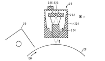
各光書き込み装置22は、プリントヘッドとも呼ばれ、図2,図3に示すように、対応色の帯電手段29に対し回転方向CWの直ぐ下流側であって、対応色の感光体ドラム28の周面近傍に配置される。各光書き込み装置22は、大略的には、ホルダ221に固定的に設けられた基板222と、発光素子アレイ223と、GRINレンズアレイ224と、少なくとも一つの温度センサ225と、を含む。
Each
発光素子アレイ223は、対応色の感光体ドラム28の周面とGRINレンズアレイ224を挟んで対向する。発光素子アレイ223は、図3に示すように、主走査方向(y軸方向)にライン状に配列された所定個数の発光素子226であって、典型的にはOLED(Organic Light Emitting Device)からなる発光素子226を含む。
The light emitting
上記所定個数は、例えば、数千〜一万個程度である。各発光素子226は、例えば、約50μm平方の矩形形状を有する。このような所定個数の発光素子226は、本実施形態の温度計算のために、複数のグループに分割される。具体的には、発光素子アレイ223は、主走査方向に沿って、Δy=0.5mm毎に仮想的に分割される。主走査方向にΔyの範囲に含まれる複数の発光素子226が同一グループに属する。
The predetermined number is, for example, about several thousand to 10,000. Each
GRINレンズアレイ224は、マイクロレンズアレイや集光性光伝送体アレイであって、各発光素子226の光軸方向に対向配置される。GRINレンズアレイ224は、主走査方向に配列された複数の屈折率分布型レンズ(Graded Index Lens)を含んでいる。GRINレンズアレイ224は、各発光素子226からの入射光ビームBを、対応色の感光体ドラム28の周面に集光する。
The
ここで、発光素子226の光軸と、屈折率分布型レンズの中心軸との位置関係の違いによって、発光素子226毎に屈折率分布型レンズの結像効率は異なる。このような結像効率の相違により、光書き込み装置22による感光体ドラム28の露光量にムラが生じないよう、光書き込み装置22の組立て時に初期調整が行われ、露光量が一定になるように各発光素子226の駆動電流が調整される。そして、発光素子226毎に駆動電流値は、不揮発性メモリ321に準備されたテーブルに記録される(下表1を参照)。
Here, the imaging efficiency of the gradient index lens differs for each light emitting

また、温度センサ225は、ホルダ221の外表面上に設けられ、光書き込み装置22の外気温度Tairを検出して、PH制御手段32に出力する。
The
以上の構成により、光書き込み装置22は、感光体ドラム28の周面上に、対応色の光ビームBを主走査方向に走査することが可能となる。また、感光体ドラム28は矢印CWの方向に回転するので、光ビームBは、回転方向CWとは逆方向の副走査方向にも走査される。これによって、各感光体ドラム28の周面には、対応色の静電潜像が形成される。
With the configuration described above, the
再度図1を参照する。各現像手段210は、y軸方向に延在し、光ビームBの照射位置の直ぐ下流で、対応色の感光体ドラム28の周面と対向する。各現像手段210は、感光体ドラム28の周面上にトナーを供給する。これによって、感光体ドラム28の周面上で静電潜像は現像され、対応色(単色)のトナー像が形成される。
Refer to FIG. 1 again. Each developing
上記現像プロセスの結果、各感光体ドラム28は、対応色のトナー像を周面上に担持する。また、各感光体ドラム28が回転することで、トナー像は回転方向CWの下流へと搬送される。
As a result of the development process, each
各転写手段23は、y軸方向に延在しており、対応色の現像手段210の下流側で、対応色の感光体ドラム28の周面と、中間転写ベルト24を挟んで対向する。
Each
中間転写ベルト24は、無端状のベルトであって、各色の転写手段23および感光体ドラム28の間に介在するように、駆動ローラ25および従動ローラ26の間に矢印αの方向に回転可能に張り渡される。また、中間転写ベルト24は、各転写手段23により各感光体ドラム28に圧接され、一次転写領域を形成する。
The
各転写手段23にはバイアス電圧が印加される。感光体ドラム28により搬送されてくるトナー像は、一次転写領域に到達すると、中間転写ベルト24の外周面に静電的に移動する(一次転写)。各色のトナー像は、中間転写ベルト24の表面の同一エリアに重なり合うよう転写される。このような合成トナー像を、中間転写ベルト24が担持しつつ回転することで二次転写ローラ27に向けて搬送する。
A bias voltage is applied to each transfer means 23. When the toner image conveyed by the
二次転写ローラ27は、中間転写ベルト24を挟んで駆動ローラ25と対向配置され、中間転写ベルト24に押圧されて、二次転写領域を形成する。二次転写ローラ27にもバイアス電圧が印加される。二次転写領域において記録媒体Sには、中間転写ベルト24により搬送されてきた合成トナー像が静電的に転写される(二次転写)。
The secondary transfer roller 27 is disposed opposite to the driving
トナー像が転写された記録媒体Sは、定着手段において加熱・加圧され、これによって、合成トナー像が記録媒体Sに定着させられる。この記録媒体Sは、排出ローラ対から排出トレイに印刷物として排出される。 The recording medium S to which the toner image has been transferred is heated and pressurized by the fixing unit, whereby the synthesized toner image is fixed to the recording medium S. The recording medium S is discharged as printed matter from the pair of discharge rollers to the discharge tray.
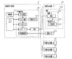
画像形成装置1は、上記各部を制御するために、制御手段3を備える。制御手段3は、CPUやメインメモリ等からなり、予め準備されたプログラムに従って動作し、画像形成装置1の印刷動作を制御する。また、制御手段3は、以下に説明する光書き込み装置22の駆動も制御する。
The
《第三欄:制御手段と基板の詳細な構成》
図4に示すように、制御手段3は、YMCK各色の光書き込み装置22の駆動制御のため、少なくとも、画像処理部31と、PH制御手段32と、を含む。
<< Third column: Detailed configuration of control means and substrate >>
As shown in FIG. 4, the
画像処理部31は、所定のページ記述言語で作成された印刷指示を受け取り、印刷すべき記録媒体S毎(換言すると、印刷ページ毎)に、ページ記述言語を解析すると共に、例えば1200dpiの二値画像を示すラスタデータを色毎に作成する。
The
PH制御手段32は、画像処理部31から受け取ったラスタデータを、色毎に、メモリ上で、光書き込み装置22の傾きを補正し(所謂、スキュー補正)、各発光素子226の発光時間を管理するためのドットカウントを行う。その後、PH制御手段32は、FFC(Flexible Flat Cable)4を介して、各色のラスタデータを、対応色の基板222に実装された駆動IC227に送信する。ここで、PH制御手段32から基板222へのデータ伝送は、例えばLVDS(Low Voltage Differential Signaling)のように、80MHz程度の高速伝送が可能なクロック同期のデータバスで行われることが好ましい。なお、PH制御手段32から各基板222には、各色のラスタデータに加え、クロック信号やライン同期信号の制御信号も送信される。
The
各基板222には、上記発光素子アレイ223に加え、少なくとも、駆動IC227が実装される。各駆動IC227は、対応色の各発光素子226を駆動する。この時、駆動IC227は、各発光素子226に、前述の各発光素子226の駆動電流値を後述の手法で温度補正して、各発光素子226に供給する。これによって、各発光素子226は発光して、対応色の感光体ドラム28が露光される。
In addition to the light emitting
《第五欄:本画像形成装置における初期温度設定》
次に、図5を参照して、本画像形成装置1における初期温度設定について説明する。初期温度設定は、画像形成装置1の主電源投入直後、または、図示しないパーソナルコンピュータ等から印刷指示を受け取ったときに実施される。
<< 5th column: Initial temperature setting in the image forming apparatus >>
Next, the initial temperature setting in the
まず、PH制御手段32は、温度センサ225から現在の外気温度Tairを取得して(S001)、予め定められた基準温度Tref(例えば、20℃〜30℃までの間の温度)を下回っている場合(S002)、放熱により全ての発光素子226の温度が実質的に均等になったとみなして、全てのグループAの初期温度をS001で得た外気温度Tairに設定して(S003)、図5の処理を終了する。
First, the
それに対し、S002において、現在の外気温度Tairが基準温度Trefを下回っていない場合、PH制御手段32は、下記のS004,S005を行う。 On the other hand, if the current outside air temperature Tair is not lower than the reference temperature Tref in S002, the PH control means 32 performs the following S004 and S005.
PH制御手段32は、前回の印刷プロセス終了時刻(以下、単に、前回の終了時刻という)と、同時刻での各グループの温度(以下、単に、前回の温度という)と、を不揮発性メモリ321に記憶している。S004において、PH制御手段32は、前回の終了時刻と、グループ毎の前回の温度とを読み出す。
The
また、PH制御手段32は、前回の終了時刻から、後述する時間ステップΔt(例えば、0.25秒)毎に定期的に温度センサ225から外気温度Tairを取得し、取得した外気温度Tairを不揮発性メモリ321に記憶する。即ち、PH制御手段32は、前回の終了時刻以降、外気温度Tairを定期的にモニタしている。S005において、PH制御手段32は、各時間ステップΔtでの外気温度Tairを取得する。
Further, the
その後、PH制御手段32は、グループ毎に現在の温度を、下式1の漸化式に基づき算出する。
Thereafter, the PH control means 32 calculates the current temperature for each group based on the recurrence formula of the following
ここで、温度算出の対象となるグループをA0、グループA0を基準として主走査方向側およびその逆方向側に隣接するグループをA+1,A−1とする。また、時刻t0からt0+Δtまでの間のグループA0の発熱量をQ(t0, 0)と表す。また、時刻tにおけるグループA−1, A0, A+1の温度をT(t, −1), T(t, 0), T(t, +1)と表す。 Here, it is assumed that the temperature calculation target group is A0, and the groups adjacent to the main scanning direction side and the opposite direction side are A + 1 and A-1 with reference to the group A0. Further, the heat generation amount of the group A0 between time t0 and t0 + Δt is represented as Q (t0, 0). Further, the temperatures of the groups A-1, A0, A + 1 at time t are represented as T (t, -1), T (t, 0), T (t, +1).
上式1によれば、時刻t0+ΔtでのグループA0の温度T(t0,0)は、時刻t0でのグループA0の温度T(t0, 0)と、時刻t0からt0+ΔtまでのグループA0の発熱量Q(t0, 0)と、時刻t0での隣接する領域の温度T(t0, −1),T(t0, +1)とから、算出される。
According to
なお、ρ,C,kは、基板222の密度、比熱、熱伝導率であって、既知の値である。また、α=k/ρC,βであり、既知の値である。SはグループA0に属する発光素子226が占有する基板222の表面積であって、既知の値である。また、Vは、グループA0に属する発光素子226が占有する体積であって、既知の値である。Tairは、時刻t0にて温度センサ225から得られる外気温度である。
Note that ρ, C, and k are the density, specific heat, and thermal conductivity of the
PH制御手段32は、前回の終了時刻から最初の時間ステップΔtにおける温度T(t0+Δt,0)を算出する際、T(t0,0)T(t0,−1)T(t0,+1)として、S004で読み出した前回の温度であって、該当するグループの前回の温度を、また、外気温度Tairとして不揮発性メモリ321に記憶された外気温度Tairであって、前回の終了時刻における外気温度Tairを、上式(1)に代入する。なお、前回の終了時刻から印刷指示を受け取るまでの間、発光素子226は点灯していないため、Q(t0,0)は0である。
When calculating the temperature T (t0 + Δt, 0) at the first time step Δt from the previous end time, the
以上の演算を全てのグループに対し実施して、最初の時間ステップΔtにおける温度T(t0+Δt,0)が算出される。次の時間ステップΔtにおける温度T(t0+Δt,0)を算出する際、T(t0,0)T(t0,−1)T(t0,+1)として、前回の時間ステップΔtで求めた温度であって、該当するグループの前回の温度を、また、外気温度Tairとして不揮発性メモリ321に記憶された外気温度Tairであって、前回の終了時刻から時間ステップΔtが経過後の外気温度Tairを、上式(1)に代入する。 The above calculation is performed for all the groups, and the temperature T (t0 + Δt, 0) at the first time step Δt is calculated. When calculating the temperature T (t0 + Δt, 0) at the next time step Δt, T (t0, 0) T (t0, −1) T (t0, +1) is the temperature obtained at the previous time step Δt. The previous temperature of the corresponding group is also the outside air temperature Tair stored in the nonvolatile memory 321 as the outside air temperature Tair, and the outside air temperature Tair after the elapse of the time step Δt from the previous end time is increased. Substitute into equation (1).
以上の演算を繰り返して、PH制御手段32は、グループ毎に、現時刻の温度を導出する(S006)。その後、PH制御手段32は、各グループの温度を初期温度として設定して(S007)、図5の処理を終了する。
By repeating the above calculation, the PH control means 32 derives the temperature at the current time for each group (S006). Thereafter, the
なお、図5の例示では、PH制御手段32は、外気温度をモニタリングするとして説明した。しかし、これに代えて、PH制御手段32は、グループ毎に、前回の温度と、現在の外気温度の間を補間して、補間結果から、各時間ステップΔtでの外気温度Tairを求めても構わない。ここで、具体的な補間方法は、直線補間でも良いし、予め行った実測結果から作成した関数を用いて補間しても良いし、他の方法でも良い。
In the example of FIG. 5, the
また、前述のΔtおよびΔyは、基板222の熱伝導率、各発光素子226の自己発熱量、必要な計算精度等に応じて適宜変更しても良い。また、使用されるΔyおよびΔtは、発光素子アレイ223の温度分布のコンピュータシミュレーションまたは実測結果とよく一致する値に選ばれることが望ましい。
In addition, the above-described Δt and Δy may be appropriately changed according to the thermal conductivity of the
《第六欄:本画像形成装置における素子温度算出》
以下、あるグループA0におけるある時刻t0から時刻t0+Δtまでの素子温度の変化量の算出方法について説明する。この算出方法を各グループに繰返し適用することで、グループ毎に時間ステップΔt単位で素子温度を算出することができる。
<< Sixth Column: Calculation of Element Temperature in the Image Forming Apparatus >>
Hereinafter, a method of calculating the change amount of the element temperature from a certain time t0 to a time t0 + Δt in a certain group A0 will be described. By repeatedly applying this calculation method to each group, the element temperature can be calculated in units of time step Δt for each group.
本実施形態に係る素子温度の算出方法は、図6に示すように、グループ毎の発熱量の算出ステップと、グループ毎の温度計算ステップと、補間による各発光素子226の温度計算ステップと、を含む(S101〜S103)。
As shown in FIG. 6, the element temperature calculation method according to the present embodiment includes a heat generation amount calculation step for each group, a temperature calculation step for each group, and a temperature calculation step for each light emitting
図6の処理は、画像形成装置1が印刷指示を受け取った時に、印刷すべき全てのページについてまとめて実施されても良いし、1ページを印刷するたびに次のページについて実施されても良い。
The processing in FIG. 6 may be performed for all pages to be printed when the
次に、図6のS101(即ち、グループ毎の発熱量の算出ステップ)の処理を、図7を参照して詳説する。以下の説明では、発熱量の算出対象をグループA0とする。
図7において、PH制御手段32は、画像処理部31で生成されたラスタデータにおいて、時刻t0からt0+Δtまでの間に感光体ドラム28に書込むべきデータに基づき、グループA0に属する発光素子226毎に、時間ステップΔtにおける発光時間を導出する(S201)。
Next, the processing of S101 in FIG. 6 (that is, the step of calculating the calorific value for each group) will be described in detail with reference to FIG. In the following description, the calorific value calculation target is group A0.
In FIG. 7, the PH control means 32 is arranged for each light emitting
次に、PH制御手段32は、不揮発性メモリ321から、対象となる発光素子226それぞれの駆動電流値を読み出す(S202)。
Next, the
次に、PH制御手段32は、対象となる発光素子226毎に、(発光時間)×(駆動電流値)×(駆動電圧値)×(発熱効率)から発熱量を導出する(S203)。ここで、駆動電圧値としては、発光素子226を駆動するために予め定められている値が用いられる。また、発熱効率として、予め実験により測定した値が用いられる。
Next, the
次に、PH制御手段32は、S203で導出した全ての発熱量の総和をとり、これを、時刻t0から時刻t0+ΔtでのグループA0の発熱量Q(t0,0)とする(S204)。PH制御手段32は、ラスタデータについて全時間ステップΔtにおいてグループ毎に発熱量Q(t0,0)を導出して、図7の処理を終了する。 Next, the PH control means 32 takes the sum of all the calorific values derived in S203 and sets this as the calorific value Q (t0, 0) of the group A0 from time t0 to time t0 + Δt (S204). The PH control means 32 derives the calorific value Q (t0, 0) for each group in the entire time step Δt for the raster data, and ends the process of FIG.
なお、対象となる発光素子226間の発熱効率が例えば±5%以上のばらついている場合には、基板222の製造時に発光素子226毎に発熱効率を測定しておき、S203で、発光素子226毎に発熱効率を使用すれば良い。
If the heat generation efficiency between the target
次に、図6に示すS102(即ち、グループ毎の温度の算出ステップの処理を詳説する。PH制御手段32は、グループ毎の温度算出に、前式(1)の漸化式を使用する。
Next, S102 shown in FIG. 6 (that is, the processing of the temperature calculation step for each group will be described in detail. The
![]()
![]()
PH制御手段32は、今回の印刷開始時刻から最初の時間ステップΔtにおける温度T(t0+Δt,0)を算出する際、T(t0,0)T(t0,−1)T(t0,+1)として、前述の初期温度設定で設定された初期温度であって、該当するグループの初期温度を、また、外気温度Tairとしては、温度センサ225で取得された外気温度Tairを、上式(1)に代入する。なお、印刷開始より発光素子226は点灯するため、Q(t0,0)は初期温度設定とは異なり0ではなく、S203で得られた値が代入される。
The
以上の演算を全てのグループに対し実施して、最初の時間ステップΔtにおける温度T(t0+Δt,0)が算出される。次の時間ステップΔtにおける温度T(t0+Δt,0)を算出する際、T(t0,0),T(t0,−1),T(t0,+1)として、前回の時間ステップΔtで求めた温度であって、該当するグループの前回の温度を、また、Q(t0,0)として図7の処理で求めた値であって該当するグループの値を、上式(1)に代入する。 The above calculation is performed for all the groups, and the temperature T (t0 + Δt, 0) at the first time step Δt is calculated. When calculating the temperature T (t0 + Δt, 0) at the next time step Δt, the temperature obtained at the previous time step Δt as T (t0,0), T (t0, -1), T (t0, + 1) Then, the previous temperature of the corresponding group and the value obtained by the processing of FIG. 7 as Q (t0,0) and the value of the corresponding group are substituted into the above equation (1).
以上の計算を繰り返して、PH制御手段32は、全ての時間ステップΔtにおける全てのグループについて温度を算出する。なお、この時、各時間ステップΔtにおける外気気温Tairが必要となるが、これは最初の時間ステップΔtで取得された温度センサ225の外気温度Tairから補間により推定されれば良い。そして、PH制御手段32は、時間ステップΔtおよびグループ毎の温度と、現在の外気温度Tairとを、次回の初期温度設定のために不揮発性メモリ321に書き込む。
By repeating the above calculation, the PH control means 32 calculates temperatures for all groups in all time steps Δt. At this time, the outside air temperature Tair at each time step Δt is required, and this may be estimated by interpolation from the outside air temperature Tair of the
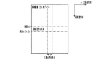
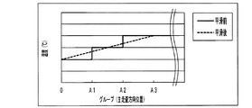
次に、図6に示すS103(即ち、各発光素子226の温度の算出ステップの処理を詳説する。PH制御手段32は、時間ステップΔt毎に得られた各グループの温度から、例えば、図8Aに示すように、各ページの中央を印刷する時刻での発光素子ごとの温度を算出する。具体的には、S102ではグループ単位で温度が算出されるため、副走査方向の中央ラインにおける各グループの温度の分布は、図8Bに示すようにステップ状の波形(実線部分を参照)となる。PH制御手段32は、このようなステップ状の各グループの温度分布を平滑化して、高周波成分を取り除く。その後、PH制御手段32は、平滑化により得られた温度分布(破線部分を参照)において、各発光素子226の主走査方向位置に対応する温度を、その発光素子226の温度とする(S103)。
Next, S103 shown in FIG. 6 (that is, the process of calculating the temperature of each light emitting
なお、本実施形態によれば、各ページの中央ラインの印刷時刻での温度が算出される。この場合、1ページを印刷する間、発光素子226の駆動電流は一定になってしまう。しかし、1ページの印刷に要する時間は、0.5〜1秒程度であるため、このような短時間での温度上昇による発光素子226の光量変動は、0.1%以下程度であるため、画像品質に実質的な影響を与えない。
According to the present embodiment, the temperature at the printing time of the center line of each page is calculated. In this case, the drive current of the
《第七欄:本画像形成装置における駆動電流の温度補正》
次に、各発光素子226に供給される駆動電流の温度補正について、図9を参照して説明する。PH制御手段32は、不揮発性メモリ321に、発光素子226のそれぞれについて、素子温度毎の発光光量を、予め定められた基準温度T1での発光光量L1を100%とした時の比で記述したテーブルを保持する。下表2には、ある発光素子226の発光光量の温度特性が示される。
<< Seventh column: Temperature correction of drive current in the image forming apparatus >>
Next, temperature correction of the drive current supplied to each light emitting
PH制御手段32は、印刷すべきページのそれぞれについて、S103で得られた各発光素子226の素子温度に対応する発光光量比を取得する(図9;S301)。PH制御手段32は、不揮発性メモリ321から、各発光素子226の駆動電流値を取得する(S302)。次に、PH制御手段32は、発光素子226毎に、駆動電流値を発光光量比で除して、補正後の駆動電流値を導出する(S303)。その後、PH制御手段32は、不揮発性メモリ321に、印刷すべきページ数に対応させて補正後の駆動電流値を記録する(S304)。
For each page to be printed, the
その後、PH制御手段32は、対象となるページが印刷される場合、不揮発性メモリ321に記録された補正後の駆動電流値を読み出し、読み出した駆動電流値を対象となる発光素子226に供給する。
Thereafter, when the target page is printed, the
《第八欄:本画像形成装置の作用・効果》
以上説明した通り、本画像形成装置1によれば、少なくとも一つの温度センサ225は必要となるものの、発光素子226毎に各種測定手段を用いることなく、各発光素子226の温度を導出することが可能となる。よって、低コストで簡単な構成で発光素子の温度を求めることが可能な光書き込み装置および画像形成装置を提供することができる。
<< Eighth column: Functions and effects of the image forming apparatus >>
As described above, according to the
さらに、副次的な効果として、算出した発光素子226の素子温度を参照することで、温度や電流密度による発光光量の劣化による光量変動の補正もより正確に行うことが可能となる。
また、発光素子226が局所的に温度上昇した際に、発光素子226の破壊を防止するための駆動停止制御を行うことができる。
また、印刷開始前や紙間において暖機運転や発光素子226の劣化度合いを揃える目的で、発光素子226の発光を行う場合に生じる温度変化にも追従することができる。
Furthermore, as a secondary effect, by referring to the calculated element temperature of the
Further, when the temperature of the
In addition, it is possible to follow a temperature change that occurs when the
《第九欄:付記》
なお、上記実施形態はOLEDに特に好適であるとして説明した。しかし、これに限らず、自己発熱により発光光量が変化する発光素子226であれば、例えばレーザダイオードにも本実施形態は適用可能である。
<Ninth column: Appendix>
In addition, the said embodiment was demonstrated as being especially suitable for OLED. However, the present embodiment is not limited to this, and the present embodiment can be applied to, for example, a laser diode as long as the
また、長時間印刷に起因して発光素子226の温度が飽和した後に関しては、PH制御手段32は、印刷終了時まで温度計算を行うのではなく、同じ温度を用い続けても良い。これによって、演算結果の保持に必要なメモリ量の節約が可能となる。この処理は、演算により得られた素子温度に閾値を設定し、演算により得られた素子温度が閾値を上回る場合は、それ以降の演算を行わない、とすることで可能である。
Further, after the temperature of the
また、式(1)に関しては、光書込み装置22または画像形成装置1の処理能力、メモリ量および補正に必要な計算精度に応じて適宜変更してもよい。例えば自己発熱の大きい発光素子を用いることや、Δtを大きく取ること等によって、対象となるグループA0の隣のグループA+1,A−1の発熱量を考慮する必要がある場合、下式(2)が使用されても良い。
Further, the expression (1) may be appropriately changed according to the processing capability of the
なお、式(2)では、外気への放熱および隣のグループA+1,A−1からの伝熱を計算する際に使用される温度を、時刻t0での温度ではなく、時刻t0での温度に、時刻t0から時刻t0+Δtの間に自己発熱による温度上昇量の半分を加えた温度とすることで、自己発熱による温度上昇を補正している。 In Equation (2), the temperature used when calculating the heat radiation to the outside air and the heat transfer from the adjacent groups A + 1 and A-1 is not the temperature at the time t0 but the temperature at the time t0. The temperature rise due to self-heating is corrected by setting the temperature to a half of the amount of temperature rise due to self-heating between time t0 and time t0 + Δt.
また、基板222に熱伝導率の低い材料を使用する場合や各発光素子226が熱伝導率の低い材料に囲まれている場合等、隣接するグループA+1,A−1からの伝熱が無視できる場合は、式(1)の代わりに、式(3)が使用されても良い。
Further, when a material with low thermal conductivity is used for the
また、本実施形態では、補正後の駆動電流を算出する際、表1に示すようなテーブルが使用されていた。しかし、これに限らず、発光素子226のそれぞれについて、素子温度を代入することで発光光量が得られる計算式が使用されても良い。
In this embodiment, a table as shown in Table 1 is used when calculating the corrected drive current. However, the present invention is not limited to this, and for each of the
本発明に係る光書き込み装置および画像形成装置は、カラー機かモノクロ機かを問わず、ファクシミリ、コピー機、プリンタおよびこれらの機能を備えた複合機に好適である。 The optical writing apparatus and the image forming apparatus according to the present invention are suitable for a facsimile machine, a copier, a printer, and a multifunction machine having these functions regardless of whether it is a color machine or a monochrome machine.
1 画像形成装置
2 プロセスユニット
22 光書き込み装置
222 基板
223 発光素子アレイ
225 温度センサ
226 発光素子
3 制御手段
32 PH制御手段
DESCRIPTION OF
Claims (8)
前記複数の発光素子が、前記主走査方向に並ぶ所定数の発光素子を含む複数のグループに分割される場合において、前記グループ毎に時刻t0から時刻t0+Δtまでの発光素子の発熱量を算出する制御手段と、
前記グループ毎に、前記グループに含まれる前記所定数の発光素子の各々の駆動電流値を記録するメモリとを備え、
前記制御手段は、
前記グループ毎に、前記グループに含まれる前記所定数の発光素子の各々に供給される駆動電流値を、前記メモリから取得する取得手段と、
前記グループ毎に、前記取得手段にて取得した前記グループに含まれる前記所定数の発光素子の各々の駆動電流値と、前記グループに含まれる前記所定数の発光素子の各々に供給される印加電圧と、前記グループに含まれる前記所定数の発光素子の各々の発熱効率と、前記グループに含まれる前記所定数の発光素子の各々が前記時刻t0から前記時刻t0+Δtまでの間に発光する発光時間と、に基づき、前記グループに含まれる前記所定数の発光素子の各々の時刻t0から時刻t0+Δtまでの発熱量を算出する第1の算出手段と、
前記グループ毎に、前記第1の算出手段にて算出した発熱量の総和をとることにより、前記グループの時刻t0から時刻t0+Δtまでの発熱量を算出する第2の算出手段とを含み、
前記制御手段はさらに、前記グループ毎に、前記時刻t0から前記時刻t0+Δtまでの発熱量と、前記時刻t0での温度とに基づき、前記時刻t0+Δtでの温度を算出する、光書き込み装置。 A plurality of light emitting elements in which the amount of emitted light changes due to self-heating, and a plurality of light emitting elements arranged in a line in the main scanning direction;
When the plurality of light emitting elements are divided into a plurality of groups including a predetermined number of light emitting elements arranged in the main scanning direction, a control for calculating a heat generation amount of the light emitting elements from time t0 to time t0 + Δt for each group. Means ,
A memory for recording a driving current value of each of the predetermined number of light emitting elements included in the group for each group;
The control means includes
Obtaining means for obtaining, for each group, a drive current value supplied to each of the predetermined number of light emitting elements included in the group from the memory;
For each group, the drive current value of each of the predetermined number of light emitting elements included in the group acquired by the acquiring unit and the applied voltage supplied to each of the predetermined number of light emitting elements included in the group And the heating efficiency of each of the predetermined number of light emitting elements included in the group, and the light emission time during which each of the predetermined number of light emitting elements included in the group emits light from the time t0 to the time t0 + Δt. , Based on the first calculation means for calculating the amount of heat generated from time t0 to time t0 + Δt of each of the predetermined number of light emitting elements included in the group;
Second calculating means for calculating a heat generation amount from time t0 to time t0 + Δt of the group by taking the sum of the heat generation amounts calculated by the first calculation means for each group;
The optical writing device, wherein the control unit further calculates, for each group, a temperature at the time t0 + Δt based on a heat generation amount from the time t0 to the time t0 + Δt and a temperature at the time t0.
前記複数の発光素子が、前記主走査方向に並ぶ所定数の発光素子を含む複数のグループに分割される場合において、前記グループ毎に時刻t0から時刻t0+Δtまでの発光素子の発熱量を算出する制御手段と、を備え、
前記制御手段はさらに、前記グループ毎に、前記時刻t0から前記時刻t0+Δtまでの発熱量と、前記時刻t0での温度とに基づき、前記時刻t0+Δtでの温度を算出し、
前記制御手段は、前記グループ毎の温度の算出に、対象となるグループにおける前記時刻t0から前記時刻t0+Δtまでの発熱量と、前記対象となるグループと隣接するグループの前記時刻t0での温度と、を用いる、光書き込み装置。 A plurality of light emitting elements in which the amount of emitted light changes due to self-heating, and a plurality of light emitting elements arranged in a line in the main scanning direction;
When the plurality of light emitting elements are divided into a plurality of groups including a predetermined number of light emitting elements arranged in the main scanning direction, a control for calculating a heat generation amount of the light emitting elements from time t0 to time t0 + Δt for each group. Means, and
The control means further calculates, for each group, a temperature at the time t0 + Δt based on a heat generation amount from the time t0 to the time t0 + Δt and a temperature at the time t0,
The control means calculates the temperature for each group, the amount of heat generated from the time t0 to the time t0 + Δt in the target group, the temperature at the time t0 of the group adjacent to the target group, An optical writing device using
前記制御手段は、前記グループ毎の温度の算出に、前記時刻t0から前記時刻t0+Δtまでの間で前記温度センサにより検出された外気温度を、さらに用いる、請求項2または3に記載の光書き込み装置。 A temperature sensor for detecting an ambient temperature around each of the light emitting elements;
4. The optical writing device according to claim 2 , wherein the control unit further uses an outside air temperature detected by the temperature sensor between the time t <b> 0 and the time t <b> 0 + Δt for calculating the temperature for each group. 5. .
前記複数の発光素子が、前記主走査方向に並ぶ所定数の発光素子を含む複数のグループに分割される場合において、前記グループ毎に時刻t0から時刻t0+Δtまでの発光素子の発熱量を算出する制御手段と、を備え、
前記制御手段はさらに、前記グループ毎に、前記時刻t0から前記時刻t0+Δtまでの発熱量と、前記時刻t0での温度とに基づき、前記時刻t0+Δtでの温度を算出し、
前記制御手段は、前記グループ毎に算出した温度分布を平滑化した後に、各前記発光素子の温度を算出する、光書き込み装置。 A plurality of light emitting elements in which the amount of emitted light changes due to self-heating, and a plurality of light emitting elements arranged in a line in the main scanning direction;
When the plurality of light emitting elements are divided into a plurality of groups including a predetermined number of light emitting elements arranged in the main scanning direction, a control for calculating a heat generation amount of the light emitting elements from time t0 to time t0 + Δt for each group. Means, and
The control means further calculates, for each group, a temperature at the time t0 + Δt based on a heat generation amount from the time t0 to the time t0 + Δt and a temperature at the time t0,
The optical writing device , wherein the control means calculates the temperature of each light emitting element after smoothing the temperature distribution calculated for each group.
Priority Applications (3)
| Application Number | Priority Date | Filing Date | Title |
|---|---|---|---|
| JP2015097892A JP6263777B2 (en) | 2015-05-13 | 2015-05-13 | Optical writing apparatus and image forming apparatus |
| US15/153,235 US9671752B2 (en) | 2015-05-13 | 2016-05-12 | Optical writing device equipped with light emitting elements |
| CN201610318036.3A CN106154785B (en) | 2015-05-13 | 2016-05-12 | Have the optical writing device of a plurality of light-emitting elements and has its image forming apparatus |
Applications Claiming Priority (1)
| Application Number | Priority Date | Filing Date | Title |
|---|---|---|---|
| JP2015097892A JP6263777B2 (en) | 2015-05-13 | 2015-05-13 | Optical writing apparatus and image forming apparatus |
Publications (2)
| Publication Number | Publication Date |
|---|---|
| JP2016210144A JP2016210144A (en) | 2016-12-15 |
| JP6263777B2 true JP6263777B2 (en) | 2018-01-24 |
Family
ID=57276999
Family Applications (1)
| Application Number | Title | Priority Date | Filing Date |
|---|---|---|---|
| JP2015097892A Active JP6263777B2 (en) | 2015-05-13 | 2015-05-13 | Optical writing apparatus and image forming apparatus |
Country Status (3)
| Country | Link |
|---|---|
| US (1) | US9671752B2 (en) |
| JP (1) | JP6263777B2 (en) |
| CN (1) | CN106154785B (en) |
Families Citing this family (4)
| Publication number | Priority date | Publication date | Assignee | Title |
|---|---|---|---|---|
| JP6776650B2 (en) * | 2016-06-23 | 2020-10-28 | 富士ゼロックス株式会社 | Printhead and image forming equipment |
| JP7191625B2 (en) * | 2018-10-04 | 2022-12-19 | キヤノン株式会社 | image forming device |
| JP7205266B2 (en) * | 2019-02-05 | 2023-01-17 | コニカミノルタ株式会社 | Optical writing device and image forming device |
| JP2024030014A (en) * | 2022-08-23 | 2024-03-07 | コニカミノルタ株式会社 | Paper type discrimination device, paper type discrimination method, and paper type discrimination program |
Family Cites Families (19)
| Publication number | Priority date | Publication date | Assignee | Title |
|---|---|---|---|---|
| JPS62280057A (en) * | 1986-05-30 | 1987-12-04 | Matsushita Graphic Commun Syst Inc | Led array head |
| JPS62299360A (en) * | 1986-06-19 | 1987-12-26 | Canon Inc | Image exposure device |
| JP2856262B2 (en) * | 1990-03-19 | 1999-02-10 | 富士通株式会社 | LED array dot position stabilization device |
| JP3234685B2 (en) * | 1993-08-17 | 2001-12-04 | ブラザー工業株式会社 | Printer printing duty control device |
| US5825399A (en) * | 1996-02-28 | 1998-10-20 | Eastman Kodak Company | Data-dependent thermal compensation for an LED printhead |
| JP3692610B2 (en) * | 1996-05-13 | 2005-09-07 | カシオ電子工業株式会社 | Color electrophotographic recording device |
| JP2003237124A (en) | 2002-02-13 | 2003-08-27 | Ricoh Elemex Corp | Thermal recorder |
| JP2003280591A (en) * | 2002-03-25 | 2003-10-02 | Sanyo Electric Co Ltd | Organic electroluminescence display device |
| US7298350B2 (en) * | 2002-09-26 | 2007-11-20 | Seiko Epson Corporation | Image forming apparatus |
| JP2006119445A (en) * | 2004-10-22 | 2006-05-11 | Fuji Photo Film Co Ltd | Organic electroluminescence exposure apparatus |
| JP4513528B2 (en) * | 2004-11-25 | 2010-07-28 | セイコーエプソン株式会社 | LIGHT EMITTING DEVICE, IMAGE FORMING DEVICE, DISPLAY DEVICE, AND LIGHT EMITTING ELEMENT DRIVE METHOD |
| JP2007296819A (en) * | 2006-05-08 | 2007-11-15 | Fuji Xerox Co Ltd | Image formation device |
| JP2008177107A (en) * | 2007-01-22 | 2008-07-31 | Seiko Epson Corp | Light-emitting device, image forming apparatus, and driving method of light-emitting device |
| JP2010052390A (en) * | 2008-08-29 | 2010-03-11 | Seiko Epson Corp | Exposure head, method of controlling exposure head, and image forming device |
| JP5338224B2 (en) * | 2008-09-25 | 2013-11-13 | カシオ計算機株式会社 | Exposure apparatus and drive control method thereof |
| JP2010120199A (en) | 2008-11-18 | 2010-06-03 | Seiko Epson Corp | Image forming apparatus and image forming method |
| JP2010240858A (en) * | 2009-04-01 | 2010-10-28 | Seiko Epson Corp | Exposure head, exposure head control method, and image forming apparatus |
| JP2014013335A (en) * | 2012-07-05 | 2014-01-23 | Canon Inc | Display device and driving method of display panel |
| JP6554775B2 (en) * | 2014-10-01 | 2019-08-07 | 株式会社リコー | Image forming apparatus |
-
2015
- 2015-05-13 JP JP2015097892A patent/JP6263777B2/en active Active
-
2016
- 2016-05-12 US US15/153,235 patent/US9671752B2/en active Active
- 2016-05-12 CN CN201610318036.3A patent/CN106154785B/en active Active
Also Published As
| Publication number | Publication date |
|---|---|
| CN106154785A (en) | 2016-11-23 |
| US20160334756A1 (en) | 2016-11-17 |
| JP2016210144A (en) | 2016-12-15 |
| CN106154785B (en) | 2019-05-14 |
| US9671752B2 (en) | 2017-06-06 |
Similar Documents
| Publication | Publication Date | Title |
|---|---|---|
| JP6263777B2 (en) | Optical writing apparatus and image forming apparatus | |
| JP6217606B2 (en) | Light emitting device and image forming apparatus | |
| JP2014228656A (en) | Image forming apparatus | |
| JP2010240858A (en) | Exposure head, exposure head control method, and image forming apparatus | |
| JP6209771B2 (en) | Image forming apparatus | |
| US10377146B2 (en) | Image forming apparatus | |
| JP6024212B2 (en) | Method for manufacturing image forming apparatus, method for adjusting light amount of print head, and method for manufacturing process cartridge | |
| JP2013163308A (en) | Image forming apparatus and image forming method | |
| JP2013233687A (en) | Light amount adjusting method for print head, method of manufacturing image forming apparatus, and method of manufacturing process cartridge | |
| JP5288732B2 (en) | Optical print head correction method, optical print head, and image forming apparatus | |
| JP2010201800A (en) | Exposure head, image forming apparatus, and image forming method | |
| JP2013242351A (en) | Light quantity adjusting method of print head and manufacturing method of image forming device | |
| JP7091192B2 (en) | Printhead and image forming equipment | |
| JP2008177107A (en) | Light-emitting device, image forming apparatus, and driving method of light-emitting device | |
| JP2010052390A (en) | Exposure head, method of controlling exposure head, and image forming device | |
| JP7073683B2 (en) | Image forming device | |
| JP2020055221A (en) | Light-emission control device and image formation device | |
| CN101654023A (en) | Exposure head, method of controlling exposure head, and image forming apparatus | |
| JP2009069663A (en) | Image forming apparatus and image forming method | |
| JP2019217666A (en) | Optical recording device and image formation device | |
| JP2016124231A (en) | Image forming apparatus, image forming method, and program | |
| JP2009119798A (en) | Signal generation circuit, exposure apparatus, image forming apparatus, and program | |
| JP2013010334A (en) | Optical print head and image forming apparatus | |
| JP2011098485A (en) | Exposure head, and control method of exposure head | |
| JP2011098486A (en) | Exposure head, control method of exposure head, and image forming apparatus |
Legal Events
| Date | Code | Title | Description |
|---|---|---|---|
| A977 | Report on retrieval |
Free format text: JAPANESE INTERMEDIATE CODE: A971007 Effective date: 20170418 |
|
| A131 | Notification of reasons for refusal |
Free format text: JAPANESE INTERMEDIATE CODE: A131 Effective date: 20170502 |
|
| A521 | Request for written amendment filed |
Free format text: JAPANESE INTERMEDIATE CODE: A523 Effective date: 20170630 |
|
| TRDD | Decision of grant or rejection written | ||
| A01 | Written decision to grant a patent or to grant a registration (utility model) |
Free format text: JAPANESE INTERMEDIATE CODE: A01 Effective date: 20171114 |
|
| A61 | First payment of annual fees (during grant procedure) |
Free format text: JAPANESE INTERMEDIATE CODE: A61 Effective date: 20171127 |
|
| R150 | Certificate of patent or registration of utility model |
Ref document number: 6263777 Country of ref document: JP Free format text: JAPANESE INTERMEDIATE CODE: R150 |