JP6263025B2 - Image processing apparatus and control method thereof - Google Patents
Image processing apparatus and control method thereof Download PDFInfo
- Publication number
- JP6263025B2 JP6263025B2 JP2013268085A JP2013268085A JP6263025B2 JP 6263025 B2 JP6263025 B2 JP 6263025B2 JP 2013268085 A JP2013268085 A JP 2013268085A JP 2013268085 A JP2013268085 A JP 2013268085A JP 6263025 B2 JP6263025 B2 JP 6263025B2
- Authority
- JP
- Japan
- Prior art keywords
- image processing
- unit
- processing unit
- image
- data
- Prior art date
- Legal status (The legal status is an assumption and is not a legal conclusion. Google has not performed a legal analysis and makes no representation as to the accuracy of the status listed.)
- Active
Links
Images


Classifications
-
- H—ELECTRICITY
- H04—ELECTRIC COMMUNICATION TECHNIQUE
- H04N—PICTORIAL COMMUNICATION, e.g. TELEVISION
- H04N1/00—Scanning, transmission or reproduction of documents or the like, e.g. facsimile transmission; Details thereof
- H04N1/00885—Power supply means, e.g. arrangements for the control of power supply to the apparatus or components thereof
- H04N1/00904—Arrangements for supplying power to different circuits or for supplying power at different levels
-
- H—ELECTRICITY
- H04—ELECTRIC COMMUNICATION TECHNIQUE
- H04N—PICTORIAL COMMUNICATION, e.g. TELEVISION
- H04N23/00—Cameras or camera modules comprising electronic image sensors; Control thereof
- H04N23/60—Control of cameras or camera modules
- H04N23/65—Control of camera operation in relation to power supply
- H04N23/651—Control of camera operation in relation to power supply for reducing power consumption by affecting camera operations, e.g. sleep mode, hibernation mode or power off of selective parts of the camera
-
- H—ELECTRICITY
- H04—ELECTRIC COMMUNICATION TECHNIQUE
- H04N—PICTORIAL COMMUNICATION, e.g. TELEVISION
- H04N23/00—Cameras or camera modules comprising electronic image sensors; Control thereof
- H04N23/60—Control of cameras or camera modules
- H04N23/667—Camera operation mode switching, e.g. between still and video, sport and normal or high- and low-resolution modes
-
- G—PHYSICS
- G03—PHOTOGRAPHY; CINEMATOGRAPHY; ANALOGOUS TECHNIQUES USING WAVES OTHER THAN OPTICAL WAVES; ELECTROGRAPHY; HOLOGRAPHY
- G03B—APPARATUS OR ARRANGEMENTS FOR TAKING PHOTOGRAPHS OR FOR PROJECTING OR VIEWING THEM; APPARATUS OR ARRANGEMENTS EMPLOYING ANALOGOUS TECHNIQUES USING WAVES OTHER THAN OPTICAL WAVES; ACCESSORIES THEREFOR
- G03B2217/00—Details of cameras or camera bodies; Accessories therefor
- G03B2217/007—Details of energy supply or management
-
- H—ELECTRICITY
- H04—ELECTRIC COMMUNICATION TECHNIQUE
- H04N—PICTORIAL COMMUNICATION, e.g. TELEVISION
- H04N25/00—Circuitry of solid-state image sensors [SSIS]; Control thereof
- H04N25/70—SSIS architectures; Circuits associated therewith
- H04N25/71—Charge-coupled device [CCD] sensors; Charge-transfer registers specially adapted for CCD sensors
- H04N25/745—Circuitry for generating timing or clock signals
Description
本発明は、撮像して得た画像の記録装置へ記録、及び表示装置へ表示処理を行う画像処理技術に関するものである。 The present invention relates to an image processing technique for recording an image obtained by capturing an image on a recording device and performing display processing on a display device.
近年、デジタルカメラ等の撮像機能を有する画像処理装置において、画像の高解像度化による処理データ量の増加や、静止画連写コマ数、動画フレームレートの向上等に伴い、データを高速に処理することの重要性が益々高くなってきている。しかし一方で、大量の画像データを高速に処理することにより画像処理装置の消費電力が増加してしまうという問題があり、このデータ処理速度と消費電力の両立が大きな課題となっている。デジタルカメラや撮像機能を有する携帯端末は、バッテリーで動作するものであるので、消費電力を削減して撮影可能枚数を増やすことが求められる。その為には特に画像記録前の撮像画像モニタ表示時における消費電力をできるだけ低く抑えることが重要となる。 In recent years, in an image processing apparatus having an imaging function such as a digital camera, the data is processed at a high speed as the amount of processing data increases due to higher resolution of the image, the number of still images continuously shot, and the moving image frame rate improve. The importance of this is getting higher and higher. However, on the other hand, there is a problem that the power consumption of the image processing apparatus increases by processing a large amount of image data at a high speed, and it is a big problem to achieve both the data processing speed and the power consumption. Since a digital camera or a portable terminal having an imaging function operates on a battery, it is required to reduce power consumption and increase the number of images that can be captured. For that purpose, it is particularly important to keep power consumption as low as possible when displaying a captured image monitor before image recording.
従来より、このようなデータ処理速度と消費電力の両立を図る様々な技術が知られている。特許文献1では、メモリアクセス許可待機時はデータ転送制御装置へのクロック供給を停止することで、データ処理速度と消費電力の両立を図っている。また、特許文献2では、データ転送に必要なクロック数に応じた最小限のクロック周波数を設定することで、データ処理速度と消費電力の両立を図っている。 Conventionally, various techniques for achieving both such data processing speed and power consumption are known. In Patent Document 1, the clock supply to the data transfer control device is stopped at the time of waiting for memory access permission, thereby achieving both data processing speed and power consumption. In Patent Document 2, a minimum clock frequency corresponding to the number of clocks necessary for data transfer is set to achieve both data processing speed and power consumption.
しかしながら、上述の従来技術はクロック数、及びクロック周波数の最適化に有効であるが、供給電力の最適化は考慮されておらず、データ転送期間中は各データ処理回路に電力を供給し続ける必要がある。何故なら、一般的なデータ処理装置のデータ転送間隔は数十nsec〜数μsecに対して電源の立ち上げシーケンスは数百μsec以上要する為、データ1転送毎に電力の供給を停止しているとデータ処理速度が著しく劣化してしまうからである。また、通常、データ処理回路への電力供給を停止するとCPU等がデータ処理回路に設定した設定値情報も失われる為、データ1転送毎に電力供給を停止すると、その度に再設定時間が必要になり、データ処理速度が著しく劣化してしまう。また、データ転送制御シーケンスも複雑になってしまう。また、上述の従来技術はクロック制御構成も複雑になってしまっている。 However, although the above-described conventional technology is effective in optimizing the number of clocks and the clock frequency, optimization of supply power is not considered and it is necessary to continue supplying power to each data processing circuit during the data transfer period. There is. This is because the power transfer sequence of several tens of nanoseconds to several microseconds for a general data processing apparatus requires several hundred microseconds or more, so that the power supply is stopped for each data transfer. This is because the data processing speed is significantly deteriorated. Normally, when power supply to the data processing circuit is stopped, setting value information set in the data processing circuit by the CPU or the like is also lost. Therefore, if power supply is stopped for each data transfer, a resetting time is required each time. As a result, the data processing speed is significantly deteriorated. Also, the data transfer control sequence becomes complicated. In addition, the above-described conventional technology also complicates the clock control configuration.
本発明は上記問題点に鑑みなされたものである。そして、本発明は、簡易な制御構成で各データ処理回路への電力供給とクロック供給を適切に制御することで、データ処理速度と消費電力の両立を図ることが可能な技術を提供する。 The present invention has been made in view of the above problems. The present invention provides a technique capable of achieving both data processing speed and power consumption by appropriately controlling power supply and clock supply to each data processing circuit with a simple control configuration.
この課題を解決するため、例えば本明細書における画像処理装置は以下の構成を備える。すなわち、
メモリと、
それぞれが前記メモリにアクセスして、複数画面の画像データを処理する複数の画像処理部と、
前記画像処理部により処理された画像データを記録媒体に記録する記録手段と、
前記画像処理部により処理された画像データに係る画像を表示する表示手段と、
前記記録手段による画像データの記録を行わずに、前記表示手段による画像の表示を行う非記録モードと、前記記録手段による画像データの記録を行う記録モードとを含む複数のモードの何れかを設定する手段と、
前記複数の画像処理部と前記メモリとの間のデータ転送を制御するデータ転送制御部と、
前記複数の画像処理部への電力供給を制御する電力制御部と、
前記設定されたモードに応じて前記データ転送制御部と前記電力制御部とを制御する制御手段とを有し、
前記制御手段は、前記設定されたモードに応じて前記データ転送制御部を制御して、前記複数の画像処理部のうち所定の画像処理部が所定の画像データの処理を行っている間に前記所定の画像処理部以外の他の画像処理部により前記メモリにアクセスされるデータ量を制御し、
前記制御手段は、前記非記録モードにおいて前記所定の画像処理部が前記所定の画像データを処理している間に前記他の画像処理部により前記メモリにアクセスされるデータ量が、前記記録モードにおいて前記所定の画像処理部が前記所定の画像データを処理している間に前記他の画像処理部により前記メモリにアクセスされるデータ量よりも少なくなるように、前記データ転送制御部を制御し、
前記制御手段は、前記非記録モードにおいて、前記所定の画像処理部が前記所定の画像データの処理を終了した後の前記所定の画像処理部に供給される電力が、前記所定の画像処理部が前記所定の画像データを処理しているときに前記所定の画像処理部に供給される電力よりも少なくなるように、前記電力制御部を制御することを特徴とする。
In order to solve this problem, for example, an image processing apparatus in the present specification has the following configuration. That is,
Memory,
A plurality of image processing units each accessing the memory and processing image data of a plurality of screens;
Recording means for recording the image data processed by the image processing unit on a recording medium;
Display means for displaying an image related to the image data processed by the image processing unit;
One of a plurality of modes including a non-recording mode for displaying an image by the display unit and a recording mode for recording image data by the recording unit without recording the image data by the recording unit is set. Means to
A data transfer control unit that controls data transfer between the plurality of image processing units and the memory;
A power control unit that controls power supply to the plurality of image processing units;
Control means for controlling the data transfer control unit and the power control unit according to the set mode;
The control unit controls the data transfer control unit in accordance with the set mode, and the predetermined image processing unit among the plurality of image processing units performs processing of predetermined image data. Controlling the amount of data accessed by the image processing unit other than the predetermined image processing unit;
The control means is configured so that the amount of data accessed by the other image processing unit while the predetermined image processing unit is processing the predetermined image data in the non-recording mode is in the recording mode. Controlling the data transfer control unit so that the amount of data accessed by the other image processing unit is less than the amount of data while the predetermined image processing unit is processing the predetermined image data;
In the non-recording mode, the control means is configured so that power supplied to the predetermined image processing unit after the predetermined image processing unit finishes processing the predetermined image data is determined by the predetermined image processing unit. The power control unit is controlled so as to be less than the power supplied to the predetermined image processing unit when the predetermined image data is being processed.
本発明によれば、データ処理回路への電力・クロックの供給を最適に制御することができ、データ処理速度と消費電力を両立した画像データの記録装置への記録、及び表示装置への表示制御を行うことができる。 According to the present invention, it is possible to optimally control the power and clock supply to the data processing circuit, and to record the image data in the recording device and to control the display on the display device that achieve both the data processing speed and the power consumption. It can be performed.
以下、添付図面に従って本発明に係る実施の形態を詳細に説明する。 Hereinafter, embodiments according to the present invention will be described in detail with reference to the accompanying drawings.
[第1の実施形態]
本発明の第1の実施の形態を説明する。図2は、第1の実施形態が適用する画像処理装置の構成を示すブロック図である。ここで示す画像処理装置は、デジタルカメラ、或いは、撮像機能を有する装置である。
[First Embodiment]
A first embodiment of the present invention will be described. FIG. 2 is a block diagram illustrating the configuration of the image processing apparatus to which the first embodiment is applied. The image processing apparatus shown here is a digital camera or an apparatus having an imaging function.
図2において、201はレンズや絞り等からなる結像光学部であり、フォーカス調節や露出調節を行う。202は光学像を電気信号に変換するCCD等の撮像素子、203は撮像素子202からのアナログ画像信号をデジタル画像データに変換するA/D変換回路である。210はDRAM211との間で画像データや各種制御データの書き込み/読み出しを行うデータ転送制御装置、204はバスを介して各種制御を司るCPUである。220は、画像データを一般的な表示装置に表示可能な輝度・色差情報等からなる画像データに変換する現像処理部である。221は、画像データに対して光学歪補正等の処理を行う補正処理部である。222は、画像データから人の顔を検出する顔画像検出部であり、顔画像検出結果は、フォーカス調節値や露出調節値として結像光学部202へフィードバックされる。223は、画像データをJPEG等、一般的な記録画像フォーマットに変換する記録画像生成部である。本第1の実施形態における各画像処理部220〜223は、DRAM211上の画像データを読み出して画像処理を施した結果をDRAM211へ書き出している。205は、画像データを表示する液晶モニタ等からなる表示部である。206は、画像データを記録媒体へ記録する記録部である。224は、220〜223の各画像処理部へのクロック・電力供給(バッテリーは不図示)をCPU204の指示により制御するパワー制御部であり、クロック・電力の供給は各画像処理部220〜223個別で制御可能な構成になっている。
In FIG. 2,
図3は、第1の実施形態に係るデータ転送制御装置210の構成を示すブロック図である。310〜313は、DRAM211から各画像処理部220〜223への読み出し画像データの転送を制御するRDDMAC(Read Direct Memory Access Controller)である。RDDMAC310〜313は、画像データを一時的に格納するFIFO320〜323を有している。330〜333は、各画像処理部220〜223のDRAM211への書き込み画像データの転送を制御するWRDMAC(Write Direct Memory Access Controller)である。WRDMAC330〜333は、画像データを一時的に格納するFIFO340〜343を有している。300は、RDDMAC310〜313、及びWRDMAC330〜333の要求により、DRAM211への読み出し画像データ、及び書き込み画像データの転送を制御するメモリアクセス制御部である。301は、RDDMAC310〜313、及びWRDMAC330〜333から同時にDRAM211へアクセス要求があった場合のアクセス優先度を制御する調停部である。
FIG. 3 is a block diagram showing the configuration of the data
図4は、第1の実施形態に係る各画像処理部220〜223がそれぞれ単独で1枚の画像データを処理した時のDRAM211へのアクセス時間とデータ量を示す図である。本実施形態では、現像処理部220が他の画像処理部と比較して多量のデータを高速に処理する。その為、現像処理部220は、他の画像処理部より多量のデータを短い周期でDRAM211へ読み出し、書き出しアクセスをし、画像処理完了時間及びDRAM211へのアクセス完了時間も速い。一般的に多量のデータを高速に処理可能な回路は消費電力が大きく、本実施形態においても現像処理部220の消費電力は他の画像処理部よりも大きい。
FIG. 4 is a diagram illustrating the access time and data amount to the
図5は、第1の実施形態に係る画像処理装置の静止画連写記録モード時において、1枚の画像データを処理して記録部206へ記録処理を実行する時の各画像処理部220〜223のDRAM211アクセスパターンを示す図である。静止画連写・記録時に各画像処理部220〜223が処理を施さなければならない画像サイズは大きい。また、連写記録モードにおいて撮影される各画面について、この画像処理部220〜223の処理全てを連写規定時間内に完了させなければならない。本実施形態の画像連写・記録時に処理する画像サイズは、横4000画素×縦3000画素、1画面当たりの処理を完了するための連写規定時間は150ミリ秒(msec)とする。ここで、ある特定の処理のDRAM211アクセスを優先させてしまうと他の処理が遅れ、連写規定時間内に全ての処理を完了させることが出来なくなる。よって、本実施形態では、連写規定時間にて、全ての処理部のDRAM211アクセスが均等に行われるように、調停部301へアクセス優先度の設定を行っている。この時、連写規定時間中は常に各画像処理部220〜223が動作している為、各画像処理部220〜223への電力・クロックは常に供給されている。本実施形態における各画像処理部220〜223は、データをDRAM211から読み出して、処理結果をDRAM211へ書き出している為、DRAM211アクセス優先度を変更することで各画像処理部220〜223の処理完了時間を柔軟に制御することは可能である。このように、全ての処理を均等にDRAM211へアクセスさせることで、各画像処理部220〜223が多量の画像データを連写規定時間内に処理し、画像を記録部206へ記録することができる。
FIG. 5 illustrates the
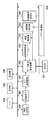
図1は、本第1の実施形態に係る画像処理装置において、記録媒体への画像記録前の、1枚の画像データを処理して表示部205へ表示する時の各画像処理部220〜222のDRAM211アクセスパターンを示す図である。デジタルカメラの場合、シャッターボタンを押下していなくても、撮像中の映像を確認するために表示部に表示する記録待機状態もしくは非記録状態となる。図示の各画像処理部220〜222のDRAM211へのアクセスパターンは、かかる状態を示していると言えば分りやすい。
FIG. 1 shows
画像表示時においても表示規定時間内に1画面の画像データに対する各処理を完了させる必要がある。ただし、非画像記録状態(非記録モード)においては、処理を施さなければならない画像サイズ(画素数)は、表示部205で表示可能なサイズ以下であればよく、静止画連写・記録時と比較して小さい。本実施形態の画像表示時に処理する画像サイズは、横640画素×縦480画素、1画面当たりの処理を完了するための表示規定時間(フレーム間隔)は30msecとする。また、非画像記録状態においては、記録部206により画像を記録する必要はない為、記録画像生成部223を動作させる必要はない。よって、画像表示時の規定時間に対する各画像処理部220〜222の処理完了時間は、静止画連写・記録時の規定時間に対する各画像処理部220〜223の処理完了時間よりも余裕がある。本実施形態では、非画像記録状態での画像表示時の表示規定時間の一部分(第1の区間101)において、CPU204は現像処理部220に電力を供給(電力供給をON)して動作させ、他の画像処理部221〜222は動作させずに電力・クロックの供給も停止(電力供給をOFF)する。そして、表示規定時間の残りの部分(第2の区間102)で、残りの処理部の電力・クロックの供給を行う。
Even when an image is displayed, it is necessary to complete each process for the image data of one screen within the prescribed display time. However, in the non-image recording state (non-recording mode), the image size (number of pixels) that must be processed may be equal to or smaller than the size that can be displayed on the
即ち、表示規定時間内の第1の区間で、現像処理部220が1枚の画像データの処理を完了したら、CPU204は現像処理部220への電力・クロックの供給を停止し、補正処理部221、顔画像検出部222へ電力・クロックを供給して処理を開始させる。本実施形態の現像処理部220は単独動作時のデータ処理速度が速い為、表示規定時間内における現像処理部220の動作期間は短く、停止期間は長くなる。本実施形態の現像処理部220の停止期間は約20msec、電力立ち上げシーケンスに要する時間は100マイクロ秒(μsec)とする。このように処理することにより、現像処理部220の停止期間が電力の立ち上げシーケンス時間より十分長くなる為、現像処理部220への電力供給を停止した場合でも、画像の表示が中断されることもない。また、本実施形態の現像処理部220は消費電力が大きい為、現像処理部220の停止期間中に電力・クロックを停止することで消費電力を大きく削減することができる。このようなDRAM211アクセスパターンは、画像連写・記録時のDRAM211アクセスパターンと比較して画像処理部220〜222の全処理完了時間は長くなる。しかし、現像処理部220の処理時間が速く、画像処理を施す画像サイズが小さく、記録画像を生成する必要がないことから、このようなDRAM211アクセスパターンでも表示規定時間内に処理を完了させることが可能となる。以上の制御を行うことにより、簡易な制御構成で電力・クロックを最適制御でき、消費電力を削減することができる。
That is, when the
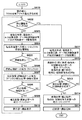
図6に本実施形態における、画像表示・記録の処理シーケンスを示す。 FIG. 6 shows an image display / recording processing sequence in this embodiment.
CPU204は、データ転送制御装置210の調停部301に対し、各画像処理部220〜223を均等にDRAM211アクセスさせるための優先度の設定を行う(S601)。CPU204は、ユーザによって静止画撮影のスイッチが押されているかを判断し(S602)、押されていなければ画像データを表示部205へ表示する為に以下の処理(S603〜S610)を行う。以下の説明は、非記録モード時の表示処理の手順である。この撮影スイッチが操作されると、非記録モードから、記録モードに切り替えられる。
The
CPU204は、結像光学部201、撮像素子202、A/D変換回路203、データ転送制御装置210に表示用画像の撮像を指示する(S603)。CPU204は、パワー制御部224に現像処理部220への電力・クロック供給を指示し、現像処理部220へ現像処理の開始を指示する(S604)。CPU204は、現像処理が完了したら(S605)、パワー制御部224に現像処理部220への電力・クロックの供給停止を指示する(S606)。またCPU204は、パワー制御部224に補正処理部221、顔画像検出部222への電力・クロックの供給を指示し、補正処理部221、顔画像検出部222にそれぞれ補正処理、顔画像検出の開始を指示する(S607)。CPU204は、補正処理・顔画像検出が完了したら(S608)、パワー制御部224に補正処理部221、顔画像検出部222への電力・クロックの供給停止を指示する(S609)。CPU204は、表示部205に生成された画像の表示を指示する(S610)。
The
一方、CPU204が、ユーザによって静止画撮影のスイッチが押されているかを判断した場合の処理(S602でYes)は次の通りである。
On the other hand, the processing when the
CPU204は、結像光学部201、撮像素子202、A/D変換回路203、データ転送制御装置210に記録用画像の撮像を指示する(S611)。CPU204は、パワー制御部224に各画像処理部220〜223への電力・クロックの供給を指示し、各画像処理部220〜223にそれぞれ処理の開始を指示する(S612)。CPU204は、各画像処理が完了したら(S613)、パワー制御部224に各画像処理部220〜223への電力・クロックの供給停止を指示する(S614)。CPU204は、記録部206に生成された画像の記録を指示する(S615)。
The
このように、非記録モードでは、複数の処理回路のうち消費電力が大きい所定の処理回路が所定のデータ量、例えば1画面の画像データの処理を開始してから完了するまでの間に他の処理回路のメモリアクセスを停止させる。このように、非記録モードでは、所定の処理回路によるメモリアクセスを集中させて処理を行う。そして、所定の処理回路がメモリにアクセスしていない期間に、電力供給やクロックの供給を停止する。このような制御を行うことで、簡易な制御構成で各画像処理部(処理回路)への電力制御、クロック供給制御を行うことができ、消費電力を削減することができる。これにより、画像記録時はデータを高速に処理し、画像表示時は消費電力を低く抑えながら規定時間内に画像表示処理を完了させることができ、データ処理速度と消費電力の両立を図ることができる。 As described above, in the non-recording mode, a predetermined processing circuit with high power consumption among a plurality of processing circuits starts processing a predetermined amount of data, for example, image data of one screen, and then completes other processing. The memory access of the processing circuit is stopped. Thus, in the non-recording mode, processing is performed by concentrating memory accesses by a predetermined processing circuit. Then, power supply and clock supply are stopped during a period when the predetermined processing circuit is not accessing the memory. By performing such control, power control and clock supply control to each image processing unit (processing circuit) can be performed with a simple control configuration, and power consumption can be reduced. As a result, data can be processed at high speed during image recording, and image display processing can be completed within a specified time while keeping power consumption low during image display, thereby achieving both data processing speed and power consumption. it can.
尚、本実施形態では4つの画像処理部で画像処理を行ったが、複数の画像処理部であれば必ずしも4つでなくても良い。 In this embodiment, the image processing is performed by four image processing units. However, the number of image processing units is not necessarily four if it is a plurality of image processing units.
また、本実施形態では画像表示時において、現像処理部220が他の処理回路よりも先行して処理を開始したが、データを高速処理可能な画像処理部であれば必ずしも現像処理部220でなくても良い。つまり、消費電力の大小に応じて、メモリ(実施形態ではDRAM)を利用して処理する複数の処理回路を第1のグループ、第2のグループに分類し、表示するフレーム間隔を2つにわけた際の第1の区間で消費電力(処理するデータ量)の多い処理回路で構成される第1のグループで処理を行い、第2の区間では第1のグループへの電力供給をOFFにするようにすればよい。また、本実施形態では画像表示時において、高速処理可能な画像処理完了後に低速画像処理部の処理を開始したが、低速画像処理完了後に高速画像処理部の処理を開始しても良い。また、本実施形態では画像表示時において、1つの高速画像処理部の処理完了後に低速画像部の処理を開始したが、高速画像処理部が複数あり、高速画像処理部を順次処理後に低速画像処理部の処理を開始しても良い。また、本実施形態では画像記録時において静止画を記録したが、動画を記録しても良い。また、本実施形態では高速画像処理部が1枚の画像を処理完了後に低速画像処理部の処理を開始したが、高速画像処理と低速画像処理の切替えタイミングは、必ずしも1枚の画像処理完了時でなくても良い。また、本実施形態では高速画像処理部の処理完了後に電力とクロックの供給を停止したが、クロックのみ供給を停止しても良く、複雑なクロック制御回路を搭載しなくとも簡易な制御で消費電力を低くすることができる。また、画像表示・記録時の処理画像サイズ、規定時間は本実施形態と同じでなくても良い。また、高速画像処理部への電力供給を完全に停止させるのではなく、処理を行って以内期間に供給する電力を、処理実行中に供給する電力よりも少なくするようにしてもよい。また、また、高速画像処理部へのクロックの供給を完全に停止させるのではなく、処理を行っていない期間に供給するクロックの周波数を、処理実行中に供給する周波数よりも低くするようにしてもよい。
In the present embodiment, when the image is displayed, the
[第2の実施形態]
第2の実施の形態を説明する。本第2の実施形態に係る画像処理装置の構成、各画像処理部の単独動作時におけるDRAMアクセスパターン、各画像処理部の画像記録時におけるDRAMアクセスパターンは上記の第1の実施形態と同様である為、その説明を省略する。
[Second Embodiment]
A second embodiment will be described. The configuration of the image processing apparatus according to the second embodiment, the DRAM access pattern at the time of individual operation of each image processing unit, and the DRAM access pattern at the time of image recording by each image processing unit are the same as those in the first embodiment. Since there is, explanation is omitted.
本第2の実施形態では、データ転送制御装置の構成、及び各画像処理部の画像表示時におけるDRAMアクセスパターンが第1実施形態と異なる。第1実施形態では、非記録モードでは、現像処理部202による1画面の処理が完了するまで、他の処理回路によるメモリアクセスを禁止していた。しかし、撮像素子202から読み出された画像が表示部205に表示されるまでの遅延時間は短い方が望ましい為、画像表示時においても、他の処理回路による全ての画像処理ができるだけ速く完了することが望ましい。しかし、画像表示時におけるDRAMアクセスパターンを画像記録時と同じDRAMアクセスパターンにしてしまうと消費電力が増加してしまう。本第2の実施形態では、画像表示時における消費電力を低く抑えながらも、全画像処理が第1の実施形態より速く完了するようにDRAMアクセスパターンを制御する。
In the second embodiment, the configuration of the data transfer control device and the DRAM access pattern at the time of image display of each image processing unit are different from those in the first embodiment. In the first embodiment, in the non-recording mode, memory access by other processing circuits is prohibited until processing of one screen by the
図7は、本第2の実施形態に係るデータ転送制御装置210の構成を示すブロック図である。RDDMAC310〜313とRDDMAC内FIFO320〜323、WRDMAC330〜333とWRDMAC内FIFO340〜343の構成は第1の実施形態と同じである。701は、現像処理部220と接続されたRDDMAC内FIFO320、及びWRDMAC内FIFO340それぞれに格納されたデータ量を算出するFIFOデータ量算出部である。RDDMAC内FIFO320のデータ格納量が十分多ければ、直ちにDRAM211からデータを読み出さなくても、RDDMAC310は現像処理部220へ読み出しデータを出力できる為、現像処理部220の処理が滞ることはない。WRDMAC内FIFO340のデータ格納量が十分少なければ、直ちにDRAM211にデータを書き込まなくても、WRDMAC330は現像処理部220が出力する書き込みデータを受け取れる為、現像処理部220の処理が滞ることはない。
FIG. 7 is a block diagram showing the configuration of the data
710は、RDDMAC310〜313、及びWRDMAC330〜333の要求により、DRAM211への読み出し画像データ、及び書き込み画像データの転送を制御するメモリアクセス制御部である。711は、RDDMAC310〜313、及びWRDMAC330〜333から同時にDRAM211へアクセス要求があった場合のアクセス優先度を制御する調停部である。本第2の実施形態の調停部711には、CPU204からRDDMAC内FIFO320のデータ格納量に対する閾値、WRDMAC内FIFO340のデータ格納量に対する閾値が設定されている。画像表示時において調停部711は、現像処理部220動作期間中のDRAM211アクセスの優先度をFIFOデータ量算出部701が出力するFIFOデータ格納量と、CPU204から設定されたデータ格納量閾値を比較して決定する。具体的には、RDDMAC内FIFO320のデータ格納量が閾値より大きく、かつWRDMAC内FIFO340のデータ格納量が閾値より小さければ、現像処理部220以外の画像処理部221〜222のDRAM211アクセスを許可する。これにより、現像処理部220のデータ処理速度に影響が少ない時に他の画像処理部221〜222に処理を行わせることができる。本実施形態では、RDDMAC内FIFO320、WRDMAC内FIFO340の容量は512バイトとする。また、RDDMAC内FIFO320のデータ格納量閾値は400バイト、WRDMAC内FIFO340のデータ格納量閾値は100バイトとする。現像処理部220の処理完了後は、FIFOデータ格納量に関係なく補正処理部221、顔画像検出部222はDRAM211へ均等にアクセスさせる。尚、画像記録時は第1の実施形態と同様、調停部711は、全画像処理部220〜223を均等にDRAM211へアクセスさせる。
A memory
図8は、本第2の実施形態に係る画像処理装置において、1枚の画像データを処理して表示部205へ表示する時の各画像処理部220〜222のDRAM211アクセスパターンを示す図である。画像表示時においてCPU204は、現像処理部220、補正処理部221、顔画像検出部222の処理を開始する。ここで調停部711には、RDDMAC内FIFO320のデータ格納量閾値、WRDMAC内FIFO340のデータ格納量閾値が設定されている。調停部711は、FIFOデータ格納量とデータ格納量閾値を比較し、現像処理部220のデータ処理速度に影響が少ないと判断される場合に、補正処理部221、顔画像検出部222のDRAM211アクセスを許可する。具体的には、RDDMAC内FIFO320のデータ格納量が閾値より大きく、かつWRDMAC内FIFO340のデータ格納量が閾値より小さければ、現像処理部220以外の画像処理部221〜222のDRAM211アクセスを許可する。現像処理部220が1枚の画像データの処理を完了したら、CPU204は現像処理部220への電力・クロックの供給を停止し、FIFOデータ格納量に関係なく補正処理部221、顔画像検出部222はDRAM211へ均等にアクセスさせる。
FIG. 8 is a diagram illustrating a
以上の制御を行うことにより、現像処理部220のデータ処理速度に影響が少ない時に他の画像処理部221〜222が処理を行うことができ、消費電力を低く抑えながらも画像処理部の全ての処理が完了する時間を短くすることができる。
By performing the above control, the other
図9に本第2の実施形態における、画像表示・記録シーケンスを示し、以下、同図に従って説明する。 FIG. 9 shows an image display / recording sequence in the second embodiment, which will be described below with reference to FIG.
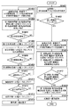
CPU204は、ユーザによって静止画撮影のスイッチが押されているかを判断し(S901)、押されていなければ画像データを表示部205へ表示する為に以下の処理(S902〜S909)を行う。CPU204は、データ転送制御装置700の調停部711に対し、FIFOデータ格納量閾値、及び設定された閾値に応じてDRAM211へのアクセス優先度を決定するモードを設定する(S902)。CPU204は、結像光学部201、撮像素子202、A/D変換回路203、データ転送制御装置700に表示用画像の撮像を指示する(S903)。CPU204は、パワー制御部224に現像処理部220、補正処理部221、顔画像検出部222への電力・クロック供給を指示する。また、現像処理部220、補正処理部221、顔画像検出部222へ処理開始を指示する(S904)。CPU204は、現像処理が完了したら(S905)、パワー制御部224に現像処理部220への電力・クロックの供給停止を指示する(S906)。そして、補正処理、顔検出処理が終了した場合(S907)、パワー制御部224に補正処理部221、顔画像検出部222への電力・クロックの供給停止を指示する(S908)。CPU204は、表示部205に生成された画像の表示を指示する(S909)。
The
また、CPU204が、ユーザによって静止画撮影のスイッチが押されていると判断した場合(S901がYes)、画像データを記録部206へ記録する為に以下の処理(S910〜S916)を行う。
If the
CPU204は、データ転送制御装置700の調停部711に対し、各画像処理部220〜223を均等にDRAM211アクセスさせる設定を行う(S910)。CPU204は、結像光学部201、撮像素子202、A/D変換回路203、データ転送制御装置210に記録用画像の撮像を指示する(S911)。CPU204は、パワー制御部224に各画像処理部220〜223への電力・クロックの供給を指示し、各画像処理部220〜223にそれぞれ処理の開始を指示する(S912)。CPU204は、各画像処理が完了したら(S913)、パワー制御部224に各画像処理部220〜223への電力・クロックの供給停止を指示する(S914)。CPU204は、記録部206に生成された画像の記録を指示する(S915)。
The
このように、本実施形態では、非記録モードにおいて、消費電力が大きい所定の処理回路が1画面の画像データの処理中に他の処理回路がメモリにアクセスするデータ量を、記録モードよりも少なくなるように制御する。そして、所定の処理回路がメモリにアクセスしていない期間に、電力供給やクロックの供給を停止する。以上の制御を行うことで、画像表示時において消費電力を低く抑えながらも、全画像処理部の処理完了時間を第1の実施形態より短くすることができる。 As described above, in the present embodiment, in the non-recording mode, the amount of data that other processing circuits access to the memory while the predetermined processing circuit with large power consumption processes the image data of one screen is smaller than that in the recording mode. Control to be. Then, power supply and clock supply are stopped during a period when the predetermined processing circuit is not accessing the memory. By performing the above control, the processing completion time of all the image processing units can be made shorter than that of the first embodiment while suppressing power consumption during image display.
尚、本実施形態では4つの画像処理部で画像処理を行ったが、複数の画像処理部であれば必ずしも4つでなくても良い。また、本実施形態では画像表示時において、現像処理部220のみ先行して処理を開始したが、データを高速処理可能な画像処理部であれば必ずしも現像処理部220でなくても良い。また、本実施形態では画像表示時において、1つの画像処理部のFIFOデータ格納量に応じて低速画像部の処理を開始したが、複数の画像処理部のFIFOデータ格納量に応じて低速画像処理部の処理を開始しても良い。また、本実施形態では画像表示時において、高速画像処理部の処理中にFIFOデータ格納量に応じて他の2つの画像処理部のDRAMアクセスを許可したが、DRAMアクセスを許可する画像処理部は必ずしも2つでなくても良い。また、本実施形態では画像表示時において、RDDMAC、WRDMAC両方のFIFOデータ格納量に応じてDRAMアクセス優先度を制御したが、どちらか一方のFIFOデータ格納量に応じてDRAMアクセス優先度を制御しても良い。また、本実施形態では画像記録時において静止画を記録したが、動画を記録しても良い。また、本実施形態では高速画像処理部の処理完了後に電力とクロックの供給を停止したが、クロックのみ供給を停止しても良く、複雑なクロック制御回路を搭載しなくとも簡易な制御で消費電力を低くすることができる。また、画像表示・記録時の処理画像サイズ、規定時間、及びデータ転送制御装置のFIFO容量、FIFOデータ格納量閾値は本実施形態と同じでなくても良い。
In this embodiment, the image processing is performed by four image processing units. However, the number of image processing units is not necessarily four if it is a plurality of image processing units. In the present embodiment, when the image is displayed, only the
[第3の実施形態]
第3の実施の形態を説明する。本第3の実施形態では、画像処理装置の構成、各画像処理部の単独動作時におけるDRAMアクセスパターン、各画像処理部の画像記録時、及び画像表示時におけるDRAMアクセスパターンが第1、第2の実施形態と異なる。本第3の実施形態では、画像表示時における消費電力を低く抑えながらも、全画像処理が第1の実施形態より速く完了するように、第2実施形態とは異なる制御手法でDRAMアクセスパターンを制御する。
[Third Embodiment]
A third embodiment will be described. In the third embodiment, the configuration of the image processing apparatus, the DRAM access pattern at the time of individual operation of each image processing unit, the DRAM access pattern at the time of image recording by each image processing unit, and at the time of image display are the first and second. Different from the embodiment. In the third embodiment, the DRAM access pattern is changed by a control method different from that of the second embodiment so that the entire image processing is completed faster than the first embodiment while keeping the power consumption at the time of image display low. Control.
図10は、本第3の実施形態に係る画像処理装置の構成を示すブロック図である。上記第1、第2の実施形態と異なる点は、本第3の実施形態では現像処理部として、第1現像処理部220a、第2現像処理部220bの2つ存在する点である。第1現像処理部220a、第2現像処理部220bは、それぞれDRAM211からの画像データを読み出して画像処理を施した結果をDRAM211へ書き込んでいる。第2現像処理部220bは、第1現像処理部220aが画像処理を施した結果に対して、画像処理を行い、その処理結果をDRAM211へ書き込んでいる。240は、各処理部220a、220b、221〜223の各画像処理部へのクロック・電力供給をCPU204の指示により制御するパワー制御部であり、クロック・電力の供給は各画像処理部220a,220b、221〜223個別で制御可能な構成になっている。第1現像処理部220a、第2現像処理部220b、パワー制御部240以外の画像処理装置の構成は第1の実施形態と同じである。
FIG. 10 is a block diagram illustrating a configuration of an image processing apparatus according to the third embodiment. The difference from the first and second embodiments is that there are two development processing units, the first
図11は、本第3の実施形態に係る各画像処理部220a,220b、221〜223がそれぞれ単独で1枚の画像データを処理した時のDRAM211へのアクセス時間とデータ量を示す図である。本実施形態では、第1現像処理部220aと第2現像処理部220bが他の画像処理部と比較して多量のデータを高速に処理し、消費電力も大きい。第1現像処理部220aと第2現像処理部220bを比較すると、第1現像処理部220aの方が第2現像処理部220bより多量のデータを高速に処理し、消費電力も大きい。また、本第3の実施形態において、各画像処理部220a,220b、221〜223のDRAM211の平均メモリ使用帯域は、それぞれ固有であって、25%、20%、15%、5%、7%である。この平均メモリ使用帯域とは、DRAM211が処理可能な最大データ処理速度[MB/sec]に対する、各画像処理部220a,220b、221〜223の平均データ処理速度[MB/sec]の比率で計算される値である。
FIG. 11 is a diagram illustrating the access time and data amount to the
図12は、本第3の実施形態に係る画像処理装置の静止画連写記録時において、1画面の画像データを処理して記録部206へ記録する時の各画像処理部220a,220b、221〜223のDRAM211アクセスパターンを示す図である。本第3の実施形態では、第1現像処理部220a、第2現像処理部220bがDRAM211へアクセスしている点が第1、第2実施形態と異なる。他の制御方法等は第1の実施形態と同じであり、連写規定時間内に全ての処理を完了させる為、全ての処理のDRAM211アクセスが均等に行われるように、調停部301へアクセス優先度の設定を行っている。
FIG. 12 shows
図13は、本第3の実施形態に係る画像処理装置の非記録状態において、1画面の画像データを処理して表示部205へ表示する時の各画像処理部220a,220b、221〜222のDRAM211アクセスパターンを示す図である。一般的に、DRAMの使用帯域が少ない時、即ち、単位時間当たりにDRAMにアクセスされるデータ量が少ないときは、DRAMへアクセスする各回路は単独動作時に近い速い処理速度で動作可能である。一方、DRAMの使用帯域が多い時は、他の回路によるアクセス完了を待たされることが多くなる為、各回路の処理速度は遅くなる。よって本実施形態では、高速画像処理部の動作時において、DRAM211の使用帯域が一定値以下であれば、低速画像処理部のDRAM211アクセスを許可する。DRAM211の使用帯域を一定値以下に制限することで、他の処理部のDRAM211アクセスによる高速画像処理部の処理速度劣化への影響を少なくしている。本第3の実施形態では、高速画像処理部の動作時におけるDRAM211の許容使用帯域を50%とし、処理部の合計使用帯域をその許容使用帯域以内に制限する。本実施形態の高速画像処理部である第1現像処理部220a、第2現像処理部220bの同時動作時におけるDRAM211の使用帯域は、45%(=25%+20%)である。ここで、顔画像検出部222を同時動作させてもDRAM211の使用帯域は50%(=25%+20%+5%)である為、本実施形態では第1現像処理部220a、第2現像処理部220b、顔画像検出部222を同時に動作させる。第1現像処理部220aの処理が完了したら、第1現像処理部220aへの電力・クロックの供給を停止する。また、第1現像処理部220aが処理を完了した後はDRAM211の使用帯域は、25%(=20%+5%)となり、補正処理部221を動作させてもDRAM211の使用帯域は40%(=20%+5%+15%)である為、補正処理部221の動作を開始する。第2現像処理部220bの処理が完了したら、第2現像処理部220bへの電力・クロックの供給を停止し、顔画像検出部222の処理が完了したら、顔画像検出部222への電力・クロックの供給を停止する。このように、本実施形態では、メモリの使用帯域が所定値を超えないように、第1現像処理部220a、第2現像処理部220bに加え、他の処理部のアクセスを許可する。このような制御を実施することにより、高速画像処理部の処理速度劣化への影響を抑えながら、低速画像処理部を動作させることが出来る為、全ての画像処理の処理完了時間を短くすることができる。本実施形態の高速画像処理部である第1現像処理部220a、第2現像処理部220bは消費電力も大きい為、高速画像処理部の処理を速く完了させて電力・クロックの供給を停止することで消費電力を低く抑えることができる。
FIG. 13 illustrates the
図14に本第3の実施形態における、画像表示・記録シーケンスを示す。 FIG. 14 shows an image display / recording sequence according to the third embodiment.
CPU204は、データ転送制御装置210の調停部301に対し、各画像処理部220a,220b、221〜223を均等にDRAM211アクセスさせる優先度の設定を行う(S1401)。CPU204は、ユーザによって静止画撮影のスイッチが押されているかを判断し(S1402)、押されていなければ画像データを表示部205へ表示する為に以下の処理(S1403〜S1414)を行う。
The
CPU204は、結像光学部201、撮像素子202、A/D変換回路203、データ転送制御装置210に表示用画像の撮像を指示する(S1403)。CPU204は、パワー制御部240に現像処理部1の230、現像処理部2の231、顔画像検出部222への電力・クロック供給を指示し、第1現像処理部220a、第2現像処理部220b、顔画像検出部222処理へ処理の開始を指示する(S1404)。CPU204は、第1現像処理が完了したら(S1405)、パワー制御部240に第1現像処理部220aへの電力・クロックの供給停止を指示する(S1406)。またCPU204は、パワー制御部240に補正処理部221への電力・クロックの供給を指示し、補正処理部221に処理の開始を指示する(S1407)。CPU204は、第2現像処理が完了したら(S1408)、パワー制御部240に第2現像処理部220bへの電力・クロックの供給停止を指示する(S1409)。CPU204は、顔画像検出が完了したら(S1410)、パワー制御部240に顔画像検出部222への電力・クロックの供給停止を指示する(S1411)。CPU204は、補正処理が完了したら(S1412)、パワー制御部240に補正処理部221への電力・クロックの供給停止を指示する(S1413)。CPU204は、表示部205に生成された画像の表示を指示する(S1414)。
The
一方、S1402にて、CPU204が、ユーザによって静止画撮影のスイッチが押されたと判断した場合、画像データを記録部206へ記録する為に以下の処理(S1415〜S1419)を行う。
On the other hand, when the
CPU204は、結像光学部201、撮像素子202、A/D変換回路203、データ転送制御装置210に記録用画像の撮像を指示する(S1415)。CPU204は、パワー制御部240に各画像処理部220a,220b、221〜223への電力・クロックの供給を指示し、各画像処理部220a,220b、221〜223にそれぞれ処理の開始を指示する(S1416)。CPU204は、各画像処理が完了したら(S617)、パワー制御部240に各画像処理部220a,220b、221〜223への電力・クロックの供給停止を指示する(S1418)。CPU204は、記録部206に生成された画像の記録を指示する(S1419)。
The
以上、上記本実施形態の制御を行うことで、画像表示時において消費電力を低く抑えながらも、全画像処理部の処理完了時間を第1の実施形態より短くすることができる。 As described above, by performing the control of the present embodiment, the processing completion time of all the image processing units can be made shorter than that of the first embodiment while suppressing power consumption during image display.
尚、本実施形態では5つの画像処理部で画像処理を行ったが、必ずしも5つでなくても良い。また、本実施形態では画像表示時において、第1現像処理部220a、第2現像処理部220bが先行して処理を開始したが、データを高速処理可能な画像処理部であれば必ずしも第1現像処理部220a、第2現像処理部220bでなくても良い。また、本実施形態では画像表示時において、高速画像処理部の処理開始後に低速画像部の処理を開始したが、低速画像処理部の処理開始後に高速画像部の処理を開始しても良い。また、本実施形態では画像記録時において静止画を記録したが、動画を記録しても良い。また、本実施形態では高速画像処理部の処理完了後に電力とクロックの供給を停止したが、クロックのみ供給を停止しても良く、複雑なクロック制御回路を搭載しなくとも簡易な制御で消費電力を低くすることができる。また、画像表示・記録時の処理画像サイズ、規定時間、及びDRAM使用制限帯域は本実施形態と同じでなくても良い。
In the present embodiment, the image processing is performed by the five image processing units, but the number is not necessarily five. In the present embodiment, the first
[その他の実施形態]
また、本発明は、以下の処理を実行することによっても実現される。即ち、上述した実施形態の機能を実現するソフトウェア(プログラム)を、ネットワーク又は各種記憶媒体を介してシステム或いは装置に供給し、そのシステム或いは装置のコンピュータ(またはCPUやMPU等)がプログラムを読み出して実行する処理である。
[Other Embodiments]
The present invention can also be realized by executing the following processing. That is, software (program) that realizes the functions of the above-described embodiments is supplied to a system or apparatus via a network or various storage media, and a computer (or CPU, MPU, or the like) of the system or apparatus reads the program. It is a process to be executed.
Claims (12)
それぞれが前記メモリにアクセスして、複数画面の画像データを処理する複数の画像処理部と、
前記画像処理部により処理された画像データを記録媒体に記録する記録手段と、
前記画像処理部により処理された画像データに係る画像を表示する表示手段と、
前記記録手段による画像データの記録を行わずに、前記表示手段による画像の表示を行う非記録モードと、前記記録手段による画像データの記録を行う記録モードとを含む複数のモードの何れかを設定する手段と、
前記複数の画像処理部と前記メモリとの間のデータ転送を制御するデータ転送制御部と、
前記複数の画像処理部への電力供給を制御する電力制御部と、
前記設定されたモードに応じて前記データ転送制御部と前記電力制御部とを制御する制御手段とを有し、
前記制御手段は、前記設定されたモードに応じて前記データ転送制御部を制御して、前記複数の画像処理部のうち所定の画像処理部が所定の画像データの処理を行っている間に前記所定の画像処理部以外の他の画像処理部により前記メモリにアクセスされるデータ量を制御し、
前記制御手段は、前記非記録モードにおいて前記所定の画像処理部が前記所定の画像データを処理している間に前記他の画像処理部により前記メモリにアクセスされるデータ量が、前記記録モードにおいて前記所定の画像処理部が前記所定の画像データを処理している間に前記他の画像処理部により前記メモリにアクセスされるデータ量よりも少なくなるように、前記データ転送制御部を制御し、
前記制御手段は、前記非記録モードにおいて、前記所定の画像処理部が前記所定の画像データの処理を終了した後の前記所定の画像処理部に供給される電力が、前記所定の画像処理部が前記所定の画像データを処理しているときに前記所定の画像処理部に供給される電力よりも少なくなるように、前記電力制御部を制御する
ことを特徴とする画像処理装置。 Memory,
A plurality of image processing units each accessing the memory and processing image data of a plurality of screens;
Recording means for recording the image data processed by the image processing unit on a recording medium;
Display means for displaying an image related to the image data processed by the image processing unit;
One of a plurality of modes including a non-recording mode for displaying an image by the display unit and a recording mode for recording image data by the recording unit without recording the image data by the recording unit is set. Means to
A data transfer control unit that controls data transfer between the plurality of image processing units and the memory;
A power control unit that controls power supply to the plurality of image processing units;
Control means for controlling the data transfer control unit and the power control unit according to the set mode;
The control unit controls the data transfer control unit in accordance with the set mode, and the predetermined image processing unit among the plurality of image processing units performs processing of predetermined image data. Controlling the amount of data accessed by the image processing unit other than the predetermined image processing unit;
The control means is configured so that the amount of data accessed by the other image processing unit while the predetermined image processing unit is processing the predetermined image data in the non-recording mode is in the recording mode. Controlling the data transfer control unit so that the amount of data accessed by the other image processing unit is less than the amount of data while the predetermined image processing unit is processing the predetermined image data;
In the non-recording mode, the control means is configured so that power supplied to the predetermined image processing unit after the predetermined image processing unit finishes processing the predetermined image data is determined by the predetermined image processing unit. The image processing apparatus, wherein the power control unit is controlled so as to be less than power supplied to the predetermined image processing unit when processing the predetermined image data.
前記制御手段は、前記非記録モードにおいて、前記所定の画像処理部が前記所定の画像データを処理した後、次に前記所定の画像データの処理を開始するまで、前記所定の画像処理部に対するクロックの供給を停止するように、前記電力制御部を制御することを特徴とする請求項1または2に記載の画像処理装置。 The power control unit further controls the supply of a clock to the image processing unit,
In the non-recording mode, the control unit is configured to provide a clock for the predetermined image processing unit until the predetermined image data starts processing after the predetermined image processing unit processes the predetermined image data. The image processing apparatus according to claim 1, wherein the power control unit is controlled to stop the supply of the power.
前記制御手段は、前記非記録モードにおいて、前記所定の画像処理部が前記所定の画像データの処理を終了した後に前記所定の画像処理部に供給されるクロックの周波数が、前記所定の画像処理部が前記所定の画像データを処理しているときに前記所定の画像処理部に供給されるクロックの周波数よりも低くなくなるように、前記電力制御部を制御することを特徴とする請求項1または2に記載の画像処理装置。 The power control unit further controls the supply of a clock to the image processing unit,
In the non-recording mode, the control means is configured such that a frequency of a clock supplied to the predetermined image processing unit after the predetermined image processing unit finishes processing the predetermined image data is the predetermined image processing unit. 3. The power control unit is controlled such that when the predetermined image data is being processed, the power control unit is controlled to be lower than a frequency of a clock supplied to the predetermined image processing unit. An image processing apparatus according to 1.
ことを特徴とする請求項1から4の何れか1項に記載の画像処理装置。 5. The image processing apparatus according to claim 1, wherein the predetermined image processing unit operates at a higher speed than the other image processing units and consumes a large amount of power.
前記複数の画像処理部の一つは、前記撮像手段から出力された画像データを処理することを特徴とする請求項1から10の何れか1項に記載の画像処理装置。 Comprising imaging means,
The image processing apparatus according to claim 1, wherein one of the plurality of image processing units processes image data output from the imaging unit.
それぞれが前記メモリにアクセスして、複数画面の画像データを処理する複数の画像処理部と、
前記画像処理部により処理された画像データを記録媒体に記録する記録手段と、
前記画像処理部により処理された画像データに係る画像を表示する表示手段と、
前記記録手段による画像データの記録を行わずに、前記表示手段による画像の表示を行う非記録モードと、前記記録手段による画像データの記録を行う記録モードとを含む複数のモードの何れかを設定する手段と、
前記複数の画像処理部と前記メモリとの間のデータ転送を制御するデータ転送制御部と、
前記複数の画像処理部への電力供給を制御する電力制御部と、
前記設定されたモードに応じて前記データ転送制御部と前記電力制御部とを制御する制御手段とを有する画像処理装置の制御方法であって、
前記設定されたモードに応じて前記データ転送制御部を制御して、前記複数の画像処理部のうち所定の画像処理部が所定の画像データの処理を行っている間に前記所定の画像処理部以外の他の画像処理部により前記メモリにアクセスされるデータ量を制御し、
前記非記録モードにおいて前記所定の画像処理部が前記所定の画像データを処理している間に前記他の画像処理部により前記メモリにアクセスされるデータ量が、前記記録モードにおいて前記所定の画像処理部が前記所定の画像データを処理している間に前記他の画像処理部により前記メモリにアクセスされるデータ量よりも少なくなるように、前記データ転送制御部を制御し、
前記非記録モードにおいて、前記所定の画像処理部が前記所定の画像データの処理を終了した後の前記所定の画像処理部に供給される電力が、前記所定の画像処理部が前記所定の画像データを処理しているときに前記所定の画像処理部に供給される電力よりも少なくなるように、前記電力制御部を制御する
ことを特徴とする画像処理装置の制御方法。 Memory,
A plurality of image processing units each accessing the memory and processing image data of a plurality of screens;
Recording means for recording the image data processed by the image processing unit on a recording medium;
Display means for displaying an image related to the image data processed by the image processing unit;
One of a plurality of modes including a non-recording mode for displaying an image by the display unit and a recording mode for recording image data by the recording unit without recording the image data by the recording unit is set. Means to
A data transfer control unit that controls data transfer between the plurality of image processing units and the memory;
A power control unit that controls power supply to the plurality of image processing units;
A control method for an image processing apparatus, comprising: a control unit that controls the data transfer control unit and the power control unit according to the set mode,
The predetermined image processing unit is controlled while the predetermined image processing unit is processing predetermined image data among the plurality of image processing units by controlling the data transfer control unit according to the set mode. Controlling the amount of data accessed by the image processing unit other than the memory,
The amount of data accessed by the other image processing unit while the predetermined image processing unit is processing the predetermined image data in the non-recording mode is equal to the predetermined image processing in the recording mode. Controlling the data transfer control unit so that the amount of data accessed to the memory by the other image processing unit is reduced while the unit is processing the predetermined image data,
In the non-recording mode, power supplied to the predetermined image processing unit after the predetermined image processing unit finishes processing the predetermined image data is determined by the predetermined image processing unit. A method for controlling an image processing apparatus, comprising: controlling the power control unit so that the power supplied to the predetermined image processing unit is less than when the image processing unit is processing.
Priority Applications (2)
| Application Number | Priority Date | Filing Date | Title |
|---|---|---|---|
| JP2013268085A JP6263025B2 (en) | 2013-12-25 | 2013-12-25 | Image processing apparatus and control method thereof |
| US14/579,399 US9602723B2 (en) | 2013-12-25 | 2014-12-22 | Imaging apparatus capable of controlling power consumption and access to memory and control method thereof |
Applications Claiming Priority (1)
| Application Number | Priority Date | Filing Date | Title |
|---|---|---|---|
| JP2013268085A JP6263025B2 (en) | 2013-12-25 | 2013-12-25 | Image processing apparatus and control method thereof |
Publications (3)
| Publication Number | Publication Date |
|---|---|
| JP2015126297A JP2015126297A (en) | 2015-07-06 |
| JP2015126297A5 JP2015126297A5 (en) | 2017-02-09 |
| JP6263025B2 true JP6263025B2 (en) | 2018-01-17 |
Family
ID=53401507
Family Applications (1)
| Application Number | Title | Priority Date | Filing Date |
|---|---|---|---|
| JP2013268085A Active JP6263025B2 (en) | 2013-12-25 | 2013-12-25 | Image processing apparatus and control method thereof |
Country Status (2)
| Country | Link |
|---|---|
| US (1) | US9602723B2 (en) |
| JP (1) | JP6263025B2 (en) |
Families Citing this family (5)
| Publication number | Priority date | Publication date | Assignee | Title |
|---|---|---|---|---|
| JP2016091205A (en) * | 2014-10-31 | 2016-05-23 | キヤノン株式会社 | Image processing apparatus, control method thereof, and program |
| US10230896B2 (en) * | 2015-04-03 | 2019-03-12 | Canon Kabushiki Kaisha | Accessory for camera and storage medium storing display control program |
| JP6957231B2 (en) * | 2017-06-27 | 2021-11-02 | キヤノン株式会社 | Recording control device and its control method |
| CN112562386B (en) * | 2020-10-26 | 2021-11-30 | 四川华体照明科技股份有限公司 | Detection system for intelligent parking system |
| US11812139B1 (en) * | 2022-06-20 | 2023-11-07 | Samsung Electronics Co., Ltd. | Closed loop dynamic ISP throttling |
Family Cites Families (10)
| Publication number | Priority date | Publication date | Assignee | Title |
|---|---|---|---|---|
| JPH07231401A (en) * | 1991-02-20 | 1995-08-29 | Ricoh Co Ltd | Electronic still camera |
| JP2000196947A (en) * | 1998-12-28 | 2000-07-14 | Canon Inc | Solid-state image pickup device |
| JP2002024166A (en) * | 2000-07-05 | 2002-01-25 | Sharp Corp | Image processing system, semiconductor device using the same and digital still camera apparatus |
| JP3914404B2 (en) | 2001-09-19 | 2007-05-16 | 株式会社リコー | Power saving interface device and power saving method |
| CN101120298A (en) * | 2005-02-16 | 2008-02-06 | 松下电器产业株式会社 | Power supply control circuit and electronic circuit |
| JP4792766B2 (en) | 2005-02-25 | 2011-10-12 | カシオ計算機株式会社 | Data transfer device and imaging device |
| JP5141324B2 (en) * | 2008-03-21 | 2013-02-13 | ソニー株式会社 | Imaging apparatus, imaging apparatus control method, signal processing apparatus, and signal processing method |
| JP5230353B2 (en) * | 2008-10-24 | 2013-07-10 | キヤノン株式会社 | Imaging apparatus and control method thereof |
| JP5820720B2 (en) * | 2011-12-27 | 2015-11-24 | オリンパス株式会社 | Imaging device |
| JP6056363B2 (en) * | 2012-10-12 | 2017-01-11 | 株式会社ソシオネクスト | Processing device and control method of processing device |
-
2013
- 2013-12-25 JP JP2013268085A patent/JP6263025B2/en active Active
-
2014
- 2014-12-22 US US14/579,399 patent/US9602723B2/en active Active
Also Published As
| Publication number | Publication date |
|---|---|
| US9602723B2 (en) | 2017-03-21 |
| JP2015126297A (en) | 2015-07-06 |
| US20150181118A1 (en) | 2015-06-25 |
Similar Documents
| Publication | Publication Date | Title |
|---|---|---|
| JP6263025B2 (en) | Image processing apparatus and control method thereof | |
| US9026697B2 (en) | Data processing apparatus | |
| US7864182B2 (en) | Dynamic tile sizing in an image pipeline | |
| JP6006083B2 (en) | Imaging apparatus and imaging method | |
| US10771681B2 (en) | Imaging pickup apparatus of which display start timing and display quality are selectable, method of controlling the same | |
| JP4328906B2 (en) | Bus control method and apparatus, and digital camera | |
| US20040201693A1 (en) | Image processing system | |
| US20150066854A1 (en) | Data processing apparatus and its control method and program | |
| US20140132800A1 (en) | Image processing apparatus and image processing method | |
| US20200358949A1 (en) | Image capturing apparatus and control method therefor | |
| US11405551B2 (en) | Imaging apparatus | |
| JP4965971B2 (en) | MEMORY CONTROL DEVICE, IMAGING DEVICE, AND MEMORY CONTROL METHOD | |
| JP4284458B2 (en) | Digital camera | |
| JP2021184576A (en) | Imaging device and method for controlling imaging device | |
| US10015431B2 (en) | Image processing apparatus and image processing method including control whether or not to permit a readout request | |
| JP2019134240A (en) | Image processing device | |
| US10769095B2 (en) | Image processing apparatus | |
| JP2017076887A (en) | Image processing device, control method for the same and imaging device | |
| JP2021019313A (en) | Imaging apparatus, control method of the same and program | |
| US20240028331A1 (en) | Image processing apparatus and image processing circuit | |
| JP6659195B2 (en) | Imaging device, control method thereof, and program | |
| US11689800B2 (en) | Image capturing apparatus and method of controlling the same, and storage medium | |
| JP2012109853A (en) | Data processing device | |
| JP2017027506A (en) | Data processing device and data processing method | |
| JP7110007B2 (en) | IMAGE PROCESSING DEVICE, IMAGING DEVICE, CONTROL METHOD FOR IMAGE PROCESSING DEVICE, PROGRAM AND STORAGE MEDIUM |
Legal Events
| Date | Code | Title | Description |
|---|---|---|---|
| A521 | Request for written amendment filed |
Free format text: JAPANESE INTERMEDIATE CODE: A523 Effective date: 20161221 |
|
| A621 | Written request for application examination |
Free format text: JAPANESE INTERMEDIATE CODE: A621 Effective date: 20161221 |
|
| A977 | Report on retrieval |
Free format text: JAPANESE INTERMEDIATE CODE: A971007 Effective date: 20170823 |
|
| A131 | Notification of reasons for refusal |
Free format text: JAPANESE INTERMEDIATE CODE: A131 Effective date: 20170929 |
|
| A521 | Request for written amendment filed |
Free format text: JAPANESE INTERMEDIATE CODE: A523 Effective date: 20171101 |
|
| TRDD | Decision of grant or rejection written | ||
| A01 | Written decision to grant a patent or to grant a registration (utility model) |
Free format text: JAPANESE INTERMEDIATE CODE: A01 Effective date: 20171117 |
|
| A61 | First payment of annual fees (during grant procedure) |
Free format text: JAPANESE INTERMEDIATE CODE: A61 Effective date: 20171215 |
|
| R151 | Written notification of patent or utility model registration |
Ref document number: 6263025 Country of ref document: JP Free format text: JAPANESE INTERMEDIATE CODE: R151 |